Embed Size (px)
Citation preview

Computer Architecture:
Main Memory (Part I)
Prof. Onur Mutlu
Carnegie Mellon University

Main Memory Lectures
These slides are from the Scalable Memory Systems course taught at ACACES 2013 (July 15-19, 2013)
Course Website:
http://users.ece.cmu.edu/~omutlu/acaces2013-memory.html
This is the first lecture:
Lecture 1 (July 15, 2013): DRAM Basics and DRAM Scaling: Trends and Basics (pptx) (pdf)
2

Scalable Many-Core Memory Systems
Lecture 1, Topic 1: DRAM Basics and
DRAM Scaling
Prof. Onur Mutlu
http://www.ece.cmu.edu/~omutlu
HiPEAC ACACES Summer School 2013
July 15, 2013

The Main Memory System
Main memory is a critical component of all computing systems: server, mobile, embedded, desktop, sensor
Main memory system must scale (in size, technology, efficiency, cost, and management algorithms) to maintain performance growth and technology scaling benefits
4
Processor
and caches Main Memory Storage (SSD/HDD)

Memory System: A Shared Resource View
5
Storage
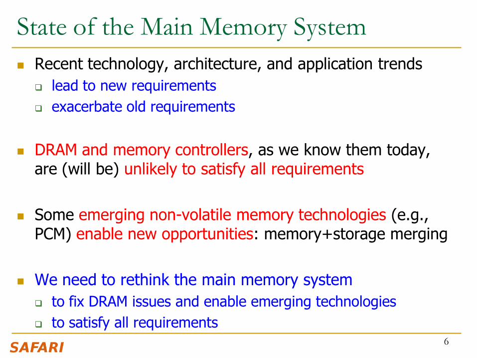
State of the Main Memory System
Recent technology, architecture, and application trends
lead to new requirements
exacerbate old requirements
DRAM and memory controllers, as we know them today, are (will be) unlikely to satisfy all requirements
Some emerging non-volatile memory technologies (e.g., PCM) enable new opportunities: memory+storage merging
We need to rethink the main memory system
to fix DRAM issues and enable emerging technologies
to satisfy all requirements
6

Major Trends Affecting Main Memory (I)
Need for main memory capacity, bandwidth, QoS increasing
Main memory energy/power is a key system design concern
DRAM technology scaling is ending
7

Major Trends Affecting Main Memory (II)
Need for main memory capacity, bandwidth, QoS increasing
Multi-core: increasing number of cores
Data-intensive applications: increasing demand/hunger for data
Consolidation: cloud computing, GPUs, mobile
Main memory energy/power is a key system design concern
DRAM technology scaling is ending
8
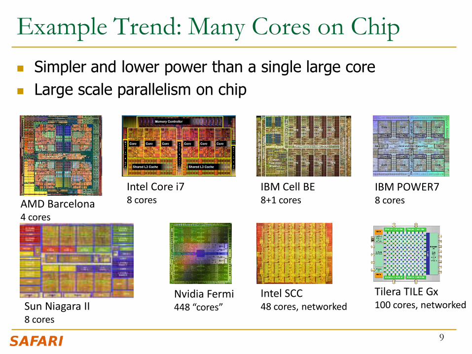
Example Trend: Many Cores on Chip
Simpler and lower power than a single large core
Large scale parallelism on chip
9
IBM Cell BE 8+1 cores
Intel Core i7 8 cores
Tilera TILE Gx 100 cores, networked
IBM POWER7 8 cores
Intel SCC 48 cores, networked
Nvidia Fermi 448 “cores”
AMD Barcelona 4 cores
Sun Niagara II 8 cores

Consequence: The Memory Capacity Gap
Memory capacity per core expected to drop by 30% every two years
Trends worse for memory bandwidth per core! 10
Core count doubling ~ every 2 years
DRAM DIMM capacity doubling ~ every 3 years

Major Trends Affecting Main Memory (III)
Need for main memory capacity, bandwidth, QoS increasing
Main memory energy/power is a key system design concern
~40-50% energy spent in off-chip memory hierarchy [Lefurgy,
IEEE Computer 2003]
DRAM consumes power even when not used (periodic refresh)
DRAM technology scaling is ending
11

Major Trends Affecting Main Memory (IV)
Need for main memory capacity, bandwidth, QoS increasing
Main memory energy/power is a key system design concern
DRAM technology scaling is ending
ITRS projects DRAM will not scale easily below X nm
Scaling has provided many benefits:
higher capacity (density), lower cost, lower energy
12

The DRAM Scaling Problem
DRAM stores charge in a capacitor (charge-based memory)
Capacitor must be large enough for reliable sensing
Access transistor should be large enough for low leakage and high retention time
Scaling beyond 40-35nm (2013) is challenging [ITRS, 2009]
DRAM capacity, cost, and energy/power hard to scale
13

Solutions to the DRAM Scaling Problem
Two potential solutions
Tolerate DRAM (by taking a fresh look at it)
Enable emerging memory technologies to eliminate/minimize DRAM
Do both
Hybrid memory systems
14

Solution 1: Tolerate DRAM Overcome DRAM shortcomings with
System-DRAM co-design
Novel DRAM architectures, interface, functions
Better waste management (efficient utilization)
Key issues to tackle
Reduce refresh energy
Improve bandwidth and latency
Reduce waste
Enable reliability at low cost
Liu, Jaiyen, Veras, Mutlu, “RAIDR: Retention-Aware Intelligent DRAM Refresh,” ISCA 2012.
Kim, Seshadri, Lee+, “A Case for Exploiting Subarray-Level Parallelism in DRAM,” ISCA 2012.
Lee+, “Tiered-Latency DRAM: A Low Latency and Low Cost DRAM Architecture,” HPCA 2013.
Liu+, “An Experimental Study of Data Retention Behavior in Modern DRAM Devices” ISCA’13.
Seshadri+, “RowClone: Fast and Efficient In-DRAM Copy and Initialization of Bulk Data,” 2013.
15

Solution 2: Emerging Memory Technologies
Some emerging resistive memory technologies seem more scalable than DRAM (and they are non-volatile)
Example: Phase Change Memory
Expected to scale to 9nm (2022 [ITRS])
Expected to be denser than DRAM: can store multiple bits/cell
But, emerging technologies have shortcomings as well
Can they be enabled to replace/augment/surpass DRAM?
Lee, Ipek, Mutlu, Burger, “Architecting Phase Change Memory as a Scalable DRAM Alternative,” ISCA 2009, CACM 2010, Top Picks 2010.
Meza, Chang, Yoon, Mutlu, Ranganathan, “Enabling Efficient and Scalable Hybrid Memories,” IEEE Comp. Arch. Letters 2012.
Yoon, Meza et al., “Row Buffer Locality Aware Caching Policies for Hybrid Memories,” ICCD 2012 Best Paper Award.
16

Hybrid Memory Systems
Meza+, “Enabling Efficient and Scalable Hybrid Memories,” IEEE Comp. Arch. Letters, 2012.
Yoon, Meza et al., “Row Buffer Locality Aware Caching Policies for Hybrid Memories,” ICCD 2012 Best Paper Award.
CPU DRAMCtrl
Fast, durable Small,
leaky, volatile, high-cost
Large, non-volatile, low-cost Slow, wears out, high active energy
PCM Ctrl DRAM Phase Change Memory (or Tech. X)
Hardware/software manage data allocation and movement to achieve the best of multiple technologies
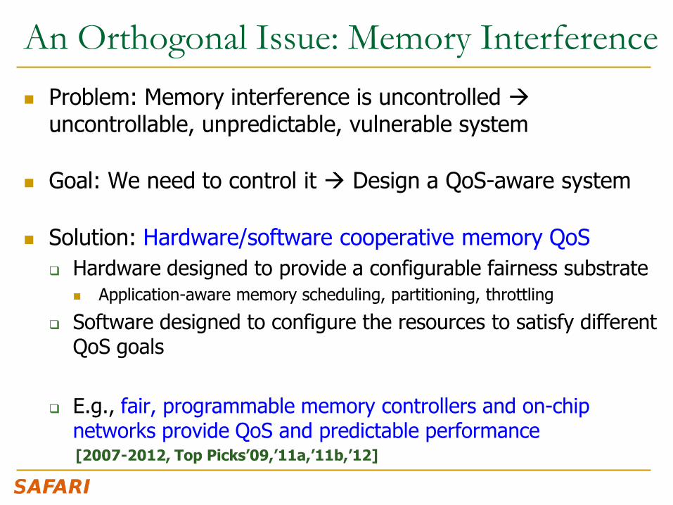
Problem: Memory interference is uncontrolled uncontrollable, unpredictable, vulnerable system
Goal: We need to control it Design a QoS-aware system
Solution: Hardware/software cooperative memory QoS
Hardware designed to provide a configurable fairness substrate
Application-aware memory scheduling, partitioning, throttling
Software designed to configure the resources to satisfy different QoS goals
E.g., fair, programmable memory controllers and on-chip networks provide QoS and predictable performance
[2007-2012, Top Picks’09,’11a,’11b,’12]
An Orthogonal Issue: Memory Interference
Agenda for Topic 1 (DRAM Scaling)
What Will You Learn in This Course
Main Memory Basics (with a Focus on DRAM)
Major Trends Affecting Main Memory
DRAM Scaling Problem and Solution Directions
Solution Direction 1: System-DRAM Co-Design
Ongoing Research
Summary
19

What Will You Learn in This Course?
Scalable Many-Core Memory Systems
July 15-19, 2013
Topic 1: Main memory basics, DRAM scaling
Topic 2: Emerging memory technologies and hybrid memories
Topic 3: Main memory interference and QoS
Topic 4 (unlikely): Cache management
Topic 5 (unlikely): Interconnects
Major Overview Reading:
Mutlu, “Memory Scaling: A Systems Architecture Perspective,” IMW 2013.
20

This Course
Will cover many problems and potential solutions related to the design of memory systems in the many core era
The design of the memory system poses many
Difficult research and engineering problems
Important fundamental problems
Industry-relevant problems
Many creative and insightful solutions are needed to solve these problems
Goal: Acquire the basics to develop such solutions (by covering fundamentals and cutting edge research)
21
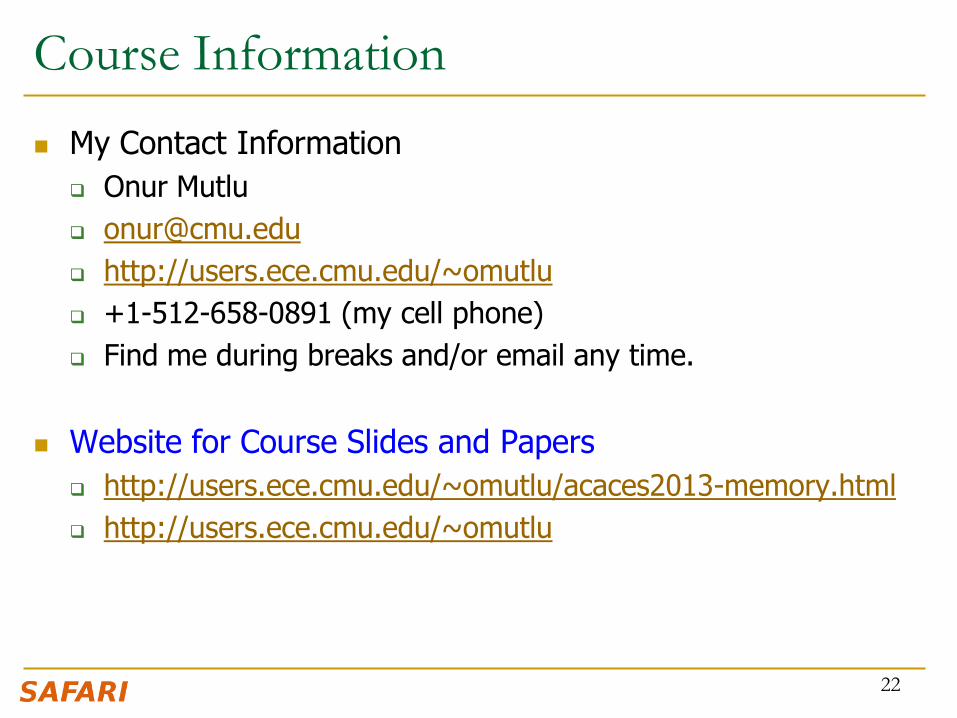
Course Information
My Contact Information
Onur Mutlu
http://users.ece.cmu.edu/~omutlu
+1-512-658-0891 (my cell phone)
Find me during breaks and/or email any time.
Website for Course Slides and Papers
http://users.ece.cmu.edu/~omutlu/acaces2013-memory.html
http://users.ece.cmu.edu/~omutlu
22

Readings and Videos
Overview Reading
Mutlu, “Memory Scaling: A Systems Architecture Perspective,” IMW 2013.
Onur Mutlu, "Memory Scaling: A Systems Architecture Perspective" Proceedings of the 5th International Memory Workshop (IMW), Monterey, CA, May 2013. Slides (pptx) (pdf)
24
Online Slides (Longer Versions)
Topic 1: DRAM Basics and DRAM Scaling
http://users.ece.cmu.edu/~omutlu/pub/onur-ACACES2013-Topic1-dram-basics-and-scaling.pptx
http://users.ece.cmu.edu/~omutlu/pub/onur-ACACES2013-Topic1-dram-basics-and-scaling.pdf
Topic 2: Emerging Technologies and Hybrid Memories
http://users.ece.cmu.edu/~omutlu/pub/onur-ACACES2013-Topic2-emerging-and-hybrid-memory-technologies.pptx
http://users.ece.cmu.edu/~omutlu/pub/onur-ACACES2013-Topic2-emerging-and-hybrid-memory-technologies.pdf
Topic 3: Memory Interference and QoS-Aware Memory Systems
http://users.ece.cmu.edu/~omutlu/pub/onur-ACACES2013-Topic3-memory-qos.pptx
http://users.ece.cmu.edu/~omutlu/pub/onur-ACACES2013-Topic3-memory-qos.pdf
25
Memory Lecture Videos
Memory Hierarchy (and Introduction to Caches)
http://www.youtube.com/watch?v=JBdfZ5i21cs&list=PL5PHm2jkkXmidJOd59REog9jDnPDTG6IJ&index=22
Main Memory
http://www.youtube.com/watch?v=ZLCy3pG7Rc0&list=PL5PHm2jkkXmidJOd59REog9jDnPDTG6IJ&index=25
Memory Controllers, Memory Scheduling, Memory QoS
http://www.youtube.com/watch?v=ZSotvL3WXmA&list=PL5PHm2jkkXmidJOd59REog9jDnPDTG6IJ&index=26
http://www.youtube.com/watch?v=1xe2w3_NzmI&list=PL5PHm2jkkXmidJOd59REog9jDnPDTG6IJ&index=27
Emerging Memory Technologies
http://www.youtube.com/watch?v=LzfOghMKyA0&list=PL5PHm2jkkXmidJOd59REog9jDnPDTG6IJ&index=35
Multiprocessor Correctness and Cache Coherence
http://www.youtube.com/watch?v=U-VZKMgItDM&list=PL5PHm2jkkXmidJOd59REog9jDnPDTG6IJ&index=32
26

Readings for Topic 1 (DRAM Scaling)
Lee et al., “Tiered-Latency DRAM: A Low Latency and Low Cost DRAM Architecture,” HPCA 2013.
Liu et al., “RAIDR: Retention-Aware Intelligent DRAM Refresh,” ISCA 2012.
Kim et al., “A Case for Exploiting Subarray-Level Parallelism in DRAM,” ISCA 2012.
Liu et al., “An Experimental Study of Data Retention Behavior in Modern DRAM Devices,” ISCA 2013.
Seshadri et al., “RowClone: Fast and Efficient In-DRAM Copy and Initialization of Bulk Data,” CMU CS Tech Report 2013.
David et al., “Memory Power Management via Dynamic Voltage/Frequency Scaling,” ICAC 2011.
Ipek et al., “Self Optimizing Memory Controllers: A Reinforcement Learning Approach,” ISCA 2008.
27
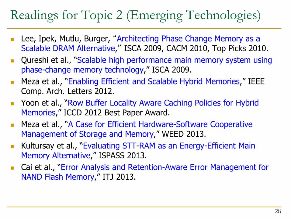
Readings for Topic 2 (Emerging Technologies)
Lee, Ipek, Mutlu, Burger, “Architecting Phase Change Memory as a Scalable DRAM Alternative,” ISCA 2009, CACM 2010, Top Picks 2010.
Qureshi et al., “Scalable high performance main memory system using phase-change memory technology,” ISCA 2009.
Meza et al., “Enabling Efficient and Scalable Hybrid Memories,” IEEE Comp. Arch. Letters 2012.
Yoon et al., “Row Buffer Locality Aware Caching Policies for Hybrid Memories,” ICCD 2012 Best Paper Award.
Meza et al., “A Case for Efficient Hardware-Software Cooperative Management of Storage and Memory,” WEED 2013.
Kultursay et al., “Evaluating STT-RAM as an Energy-Efficient Main Memory Alternative,” ISPASS 2013.
Cai et al., “Error Analysis and Retention-Aware Error Management for NAND Flash Memory,” ITJ 2013.
28

Readings for Topic 3 (Memory QoS)
Moscibroda and Mutlu, “Memory Performance Attacks,” USENIX Security 2007.
Mutlu and Moscibroda, “Stall-Time Fair Memory Access Scheduling,” MICRO 2007.
Mutlu and Moscibroda, “Parallelism-Aware Batch Scheduling,” ISCA 2008, IEEE Micro 2009.
Kim et al., “ATLAS: A Scalable and High-Performance Scheduling Algorithm for Multiple Memory Controllers,” HPCA 2010.
Kim et al., “Thread Cluster Memory Scheduling,” MICRO 2010, IEEE Micro 2011.
Muralidhara et al., “Memory Channel Partitioning,” MICRO 2011.
Ausavarungnirun et al., “Staged Memory Scheduling,” ISCA 2012.
Subramanian et al., “MISE: Providing Performance Predictability and Improving Fairness in Shared Main Memory Systems,” HPCA 2013.
Das et al., “Application-to-Core Mapping Policies to Reduce Memory System Interference in Multi-Core Systems,” HPCA 2013.
29

Readings for Topic 3 (Memory QoS)
Ebrahimi et al., “Fairness via Source Throttling,” ASPLOS 2010, ACM TOCS 2012.
Lee et al., “Prefetch-Aware DRAM Controllers,” MICRO 2008, IEEE TC 2011.
Ebrahimi et al., “Parallel Application Memory Scheduling,” MICRO 2011.
Ebrahimi et al., “Prefetch-Aware Shared Resource Management for Multi-Core Systems,” ISCA 2011.
30

Readings in Flash Memory Yu Cai, Gulay Yalcin, Onur Mutlu, Erich F. Haratsch, Adrian Cristal, Osman Unsal, and Ken Mai,
"Error Analysis and Retention-Aware Error Management for NAND Flash Memory" Intel Technology Journal (ITJ) Special Issue on Memory Resiliency, Vol. 17, No. 1, May 2013.
Yu Cai, Erich F. Haratsch, Onur Mutlu, and Ken Mai, "Threshold Voltage Distribution in MLC NAND Flash Memory: Characterization, Analysis and Modeling" Proceedings of the Design, Automation, and Test in Europe Conference (DATE), Grenoble, France, March 2013. Slides (ppt)
Yu Cai, Gulay Yalcin, Onur Mutlu, Erich F. Haratsch, Adrian Cristal, Osman Unsal, and Ken Mai, "Flash Correct-and-Refresh: Retention-Aware Error Management for Increased Flash Memory Lifetime" Proceedings of the 30th IEEE International Conference on Computer Design (ICCD), Montreal, Quebec, Canada, September 2012. Slides (ppt) (pdf)
Yu Cai, Erich F. Haratsch, Onur Mutlu, and Ken Mai, "Error Patterns in MLC NAND Flash Memory: Measurement, Characterization, and Analysis" Proceedings of the Design, Automation, and Test in Europe Conference (DATE), Dresden, Germany, March 2012. Slides (ppt)
31

Online Lectures and More Information
Online Computer Architecture Lectures
http://www.youtube.com/playlist?list=PL5PHm2jkkXmidJOd59REog9jDnPDTG6IJ
Online Computer Architecture Courses
Intro: http://www.ece.cmu.edu/~ece447/s13/doku.php
Advanced: http://www.ece.cmu.edu/~ece740/f11/doku.php
Advanced: http://www.ece.cmu.edu/~ece742/doku.php
Recent Research Papers
http://users.ece.cmu.edu/~omutlu/projects.htm
http://scholar.google.com/citations?user=7XyGUGkAAAAJ&hl=en
32

Agenda for Topic 1 (DRAM Scaling)
What Will You Learn in This Mini-Lecture Series
Main Memory Basics (with a Focus on DRAM)
Major Trends Affecting Main Memory
DRAM Scaling Problem and Solution Directions
Solution Direction 1: System-DRAM Co-Design
Ongoing Research
Summary
33

Main Memory
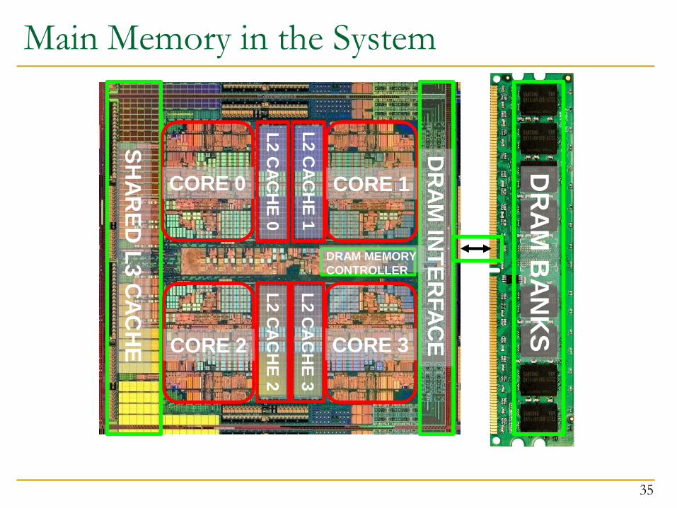
Main Memory in the System
35
CORE 1
L2
CA
CH
E 0
SH
AR
ED
L3 C
AC
HE
DR
AM
INT
ER
FA
CE
CORE 0
CORE 2 CORE 3 L
2 C
AC
HE
1
L2
CA
CH
E 2
L2
CA
CH
E 3
DR
AM
BA
NK
S
DRAM MEMORY
CONTROLLER

Ideal Memory
Zero access time (latency)
Infinite capacity
Zero cost
Infinite bandwidth (to support multiple accesses in parallel)
36

The Problem
Ideal memory’s requirements oppose each other
Bigger is slower
Bigger Takes longer to determine the location
Faster is more expensive
Memory technology: SRAM vs. DRAM
Higher bandwidth is more expensive
Need more banks, more ports, higher frequency, or faster technology
37
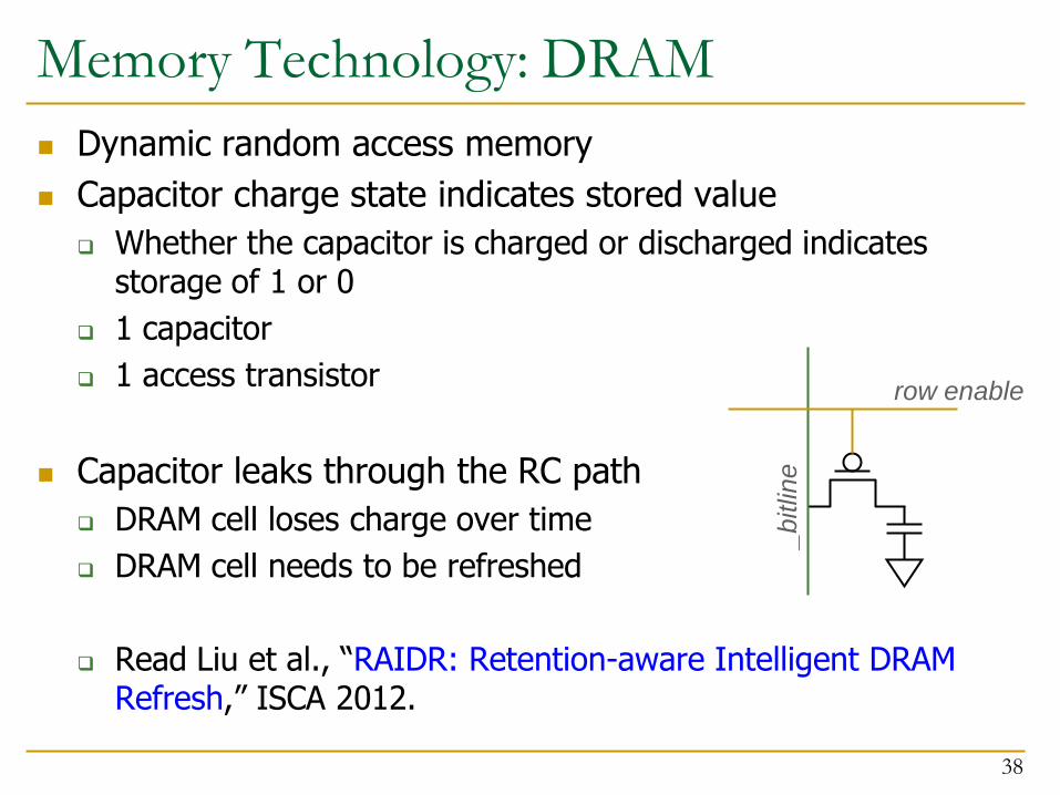
Memory Technology: DRAM
Dynamic random access memory
Capacitor charge state indicates stored value
Whether the capacitor is charged or discharged indicates storage of 1 or 0
1 capacitor
1 access transistor
Capacitor leaks through the RC path
DRAM cell loses charge over time
DRAM cell needs to be refreshed
Read Liu et al., “RAIDR: Retention-aware Intelligent DRAM Refresh,” ISCA 2012.
38
row enable
_b
itlin
e
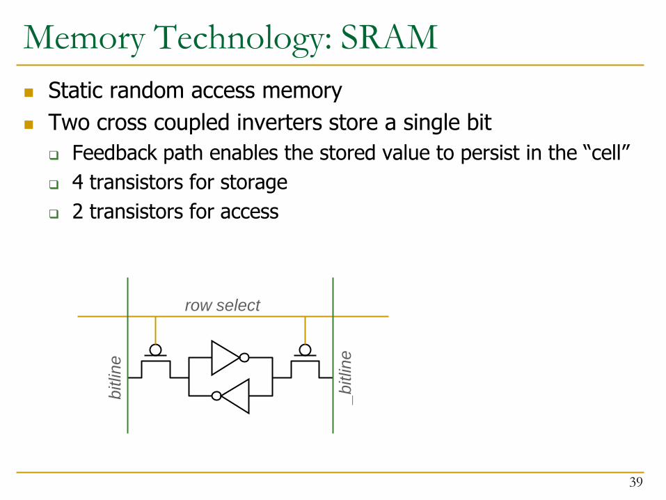
Static random access memory
Two cross coupled inverters store a single bit
Feedback path enables the stored value to persist in the “cell”
4 transistors for storage
2 transistors for access
Memory Technology: SRAM
39
row select
bitlin
e
_b
itlin
e
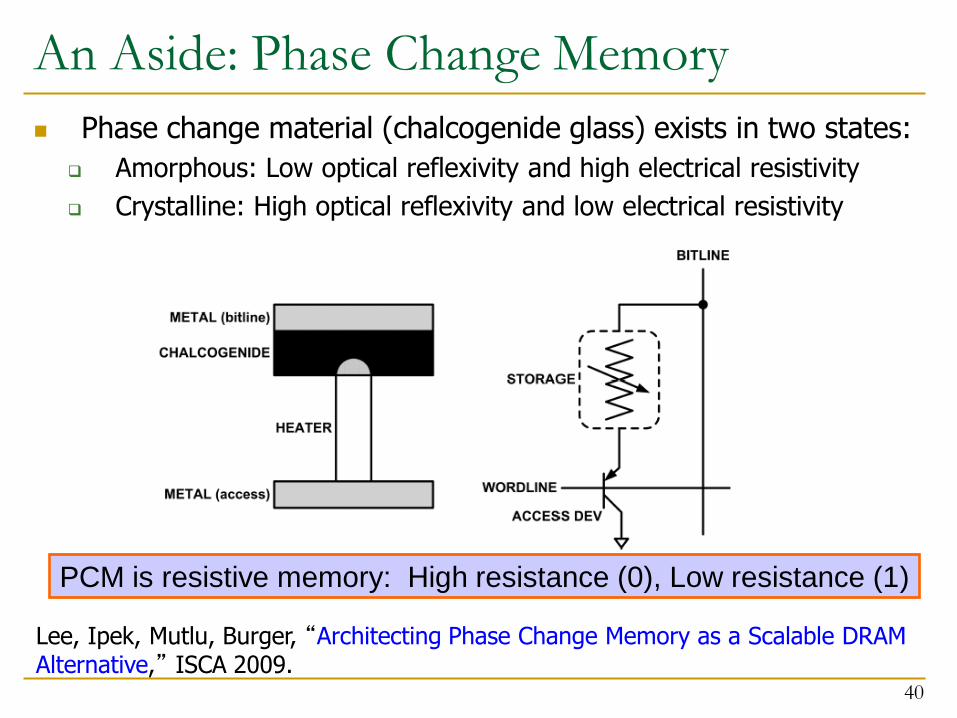
An Aside: Phase Change Memory
Phase change material (chalcogenide glass) exists in two states:
Amorphous: Low optical reflexivity and high electrical resistivity
Crystalline: High optical reflexivity and low electrical resistivity
40
PCM is resistive memory: High resistance (0), Low resistance (1)
Lee, Ipek, Mutlu, Burger, “Architecting Phase Change Memory as a Scalable DRAM Alternative,” ISCA 2009.
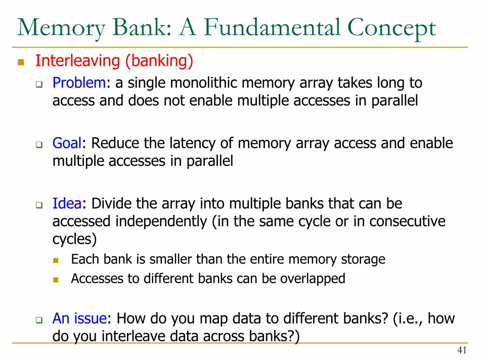
Memory Bank: A Fundamental Concept
Interleaving (banking)
Problem: a single monolithic memory array takes long to access and does not enable multiple accesses in parallel
Goal: Reduce the latency of memory array access and enable multiple accesses in parallel
Idea: Divide the array into multiple banks that can be accessed independently (in the same cycle or in consecutive cycles)
Each bank is smaller than the entire memory storage
Accesses to different banks can be overlapped
An issue: How do you map data to different banks? (i.e., how do you interleave data across banks?)
41
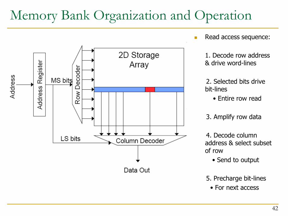
Memory Bank Organization and Operation
Read access sequence:
1. Decode row address & drive word-lines
2. Selected bits drive bit-lines
• Entire row read
3. Amplify row data
4. Decode column address & select subset of row
• Send to output
5. Precharge bit-lines
• For next access
42

Why Memory Hierarchy?
We want both fast and large
But we cannot achieve both with a single level of memory
Idea: Have multiple levels of storage (progressively bigger and slower as the levels are farther from the processor) and ensure most of the data the processor needs is kept in the fast(er) level(s)
43

Memory Hierarchy
Fundamental tradeoff
Fast memory: small
Large memory: slow
Idea: Memory hierarchy
Latency, cost, size,
bandwidth
44
CPU
Main
Memory
(DRAM)
RF
Cache
Hard Disk

Caching Basics: Exploit Temporal Locality
Idea: Store recently accessed data in automatically managed fast memory (called cache)
Anticipation: the data will be accessed again soon
Temporal locality principle
Recently accessed data will be again accessed in the near future
This is what Maurice Wilkes had in mind:
Wilkes, “Slave Memories and Dynamic Storage Allocation,” IEEE Trans. On Electronic Computers, 1965.
“The use is discussed of a fast core memory of, say 32000 words as a slave to a slower core memory of, say, one million words in such a way that in practical cases the effective access time is nearer that of the fast memory than that of the slow memory.”
45

Caching Basics: Exploit Spatial Locality
Idea: Store addresses adjacent to the recently accessed one in automatically managed fast memory
Logically divide memory into equal size blocks
Fetch to cache the accessed block in its entirety
Anticipation: nearby data will be accessed soon
Spatial locality principle
Nearby data in memory will be accessed in the near future
E.g., sequential instruction access, array traversal
This is what IBM 360/85 implemented
16 Kbyte cache with 64 byte blocks
Liptay, “Structural aspects of the System/360 Model 85 II: the cache,” IBM Systems Journal, 1968.
46
A Note on Manual vs. Automatic Management
Manual: Programmer manages data movement across levels
-- too painful for programmers on substantial programs
“core” vs “drum” memory in the 50’s
still done in some embedded processors (on-chip scratch pad SRAM in lieu of a cache)
Automatic: Hardware manages data movement across levels, transparently to the programmer
++ programmer’s life is easier
simple heuristic: keep most recently used items in cache
the average programmer doesn’t need to know about it
You don’t need to know how big the cache is and how it works to write a “correct” program! (What if you want a “fast” program?)
47

Automatic Management in Memory Hierarchy
Wilkes, “Slave Memories and Dynamic Storage Allocation,” IEEE Trans. On Electronic Computers, 1965.
“By a slave memory I mean one which automatically accumulates to itself words that come from a slower main memory, and keeps them available for subsequent use without it being necessary for the penalty of main memory access to be incurred again.”
48

A Modern Memory Hierarchy
49
Register File 32 words, sub-nsec
L1 cache ~32 KB, ~nsec
L2 cache 512 KB ~ 1MB, many nsec
L3 cache, .....
Main memory (DRAM), GB, ~100 nsec
Swap Disk 100 GB, ~10 msec
manual/compiler register spilling
automatic demand paging
Automatic HW cache management
Memory Abstraction

The DRAM Subsystem

DRAM Subsystem Organization
Channel
DIMM
Rank
Chip
Bank
Row/Column
51

Page Mode DRAM
A DRAM bank is a 2D array of cells: rows x columns
A “DRAM row” is also called a “DRAM page”
“Sense amplifiers” also called “row buffer”
Each address is a <row,column> pair
Access to a “closed row”
Activate command opens row (placed into row buffer)
Read/write command reads/writes column in the row buffer
Precharge command closes the row and prepares the bank for next access
Access to an “open row”
No need for activate command
52
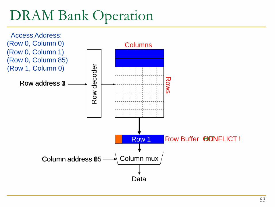
DRAM Bank Operation
53
Row Buffer
(Row 0, Column 0)
Row
de
co
de
r
Column mux
Row address 0
Column address 0
Data
Row 0 Empty
(Row 0, Column 1)
Column address 1
(Row 0, Column 85)
Column address 85
(Row 1, Column 0)
HIT HIT
Row address 1
Row 1
Column address 0
CONFLICT !
Columns
Row
s
Access Address:

The DRAM Chip
Consists of multiple banks (2-16 in Synchronous DRAM)
Banks share command/address/data buses
The chip itself has a narrow interface (4-16 bits per read)
54

128M x 8-bit DRAM Chip
55

DRAM Rank and Module
Rank: Multiple chips operated together to form a wide interface
All chips comprising a rank are controlled at the same time
Respond to a single command
Share address and command buses, but provide different data
A DRAM module consists of one or more ranks
E.g., DIMM (dual inline memory module)
This is what you plug into your motherboard
If we have chips with 8-bit interface, to read 8 bytes in a single access, use 8 chips in a DIMM
56

A 64-bit Wide DIMM (One Rank)
57
DRAM
Chip
DRAM
Chip
DRAM
Chip
DRAM
Chip
DRAM
Chip
DRAM
Chip
DRAM
Chip
DRAM
Chip
Command Data
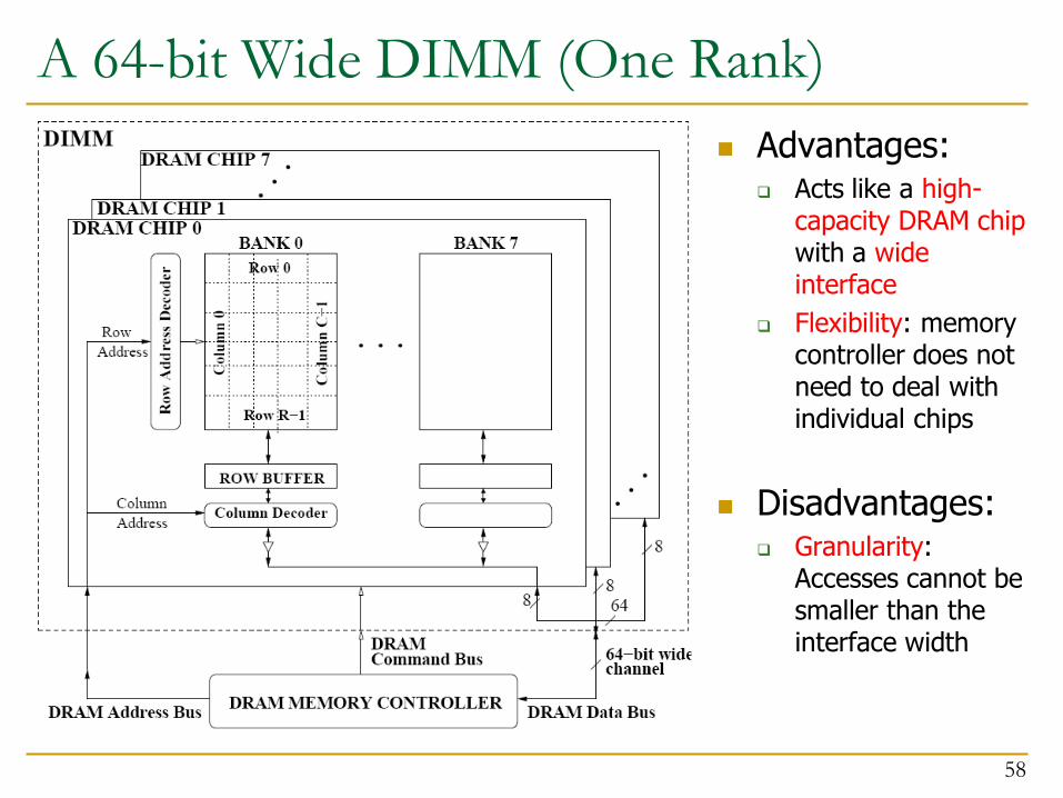
A 64-bit Wide DIMM (One Rank)
Advantages: Acts like a high-
capacity DRAM chip with a wide interface
Flexibility: memory controller does not need to deal with individual chips
Disadvantages: Granularity:
Accesses cannot be smaller than the interface width
58

Multiple DIMMs
59
Advantages:
Enables even higher capacity
Disadvantages:
Interconnect complexity and energy consumption can be high

DRAM Channels
2 Independent Channels: 2 Memory Controllers (Above)
2 Dependent/Lockstep Channels: 1 Memory Controller with wide interface (Not shown above)
60

Generalized Memory Structure
61

Generalized Memory Structure
62
Kim+, “A Case for Exploiting Subarray-Level Parallelism in DRAM,” ISCA 2012.

The DRAM Subsystem
The Top Down View
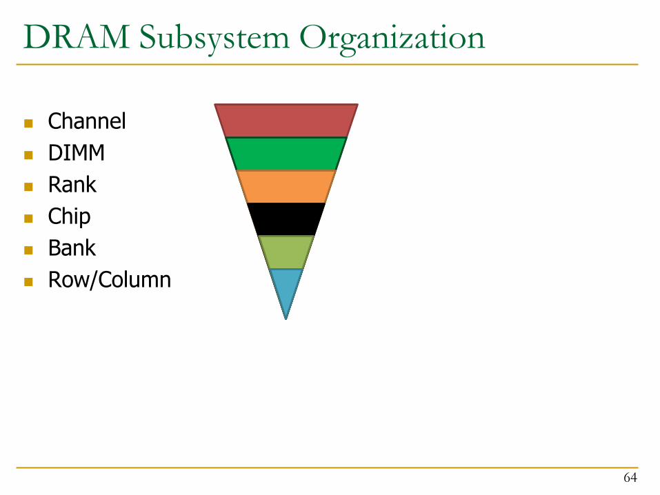
DRAM Subsystem Organization
Channel
DIMM
Rank
Chip
Bank
Row/Column
64

The DRAM subsystem
Memory channel Memory channel
DIMM (Dual in-line memory module)
Processor
“Channel”

Breaking down a DIMM
DIMM (Dual in-line memory module)
Side view
Front of DIMM Back of DIMM

Breaking down a DIMM
DIMM (Dual in-line memory module)
Side view
Front of DIMM Back of DIMM
Rank 0: collection of 8 chips Rank 1
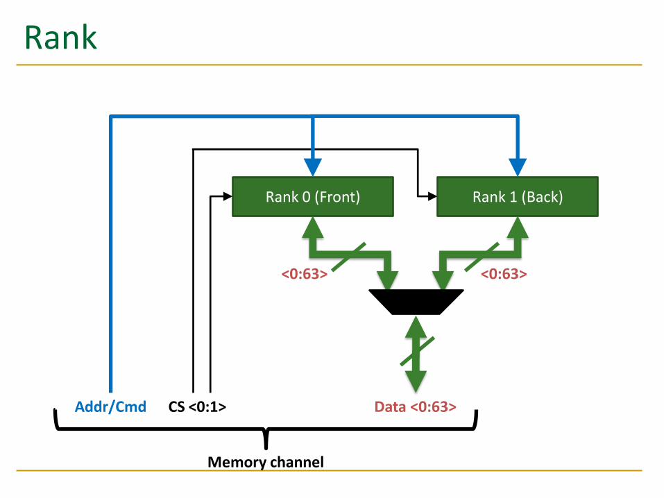
Rank
Rank 0 (Front) Rank 1 (Back)
Data <0:63> CS <0:1> Addr/Cmd
<0:63> <0:63>
Memory channel
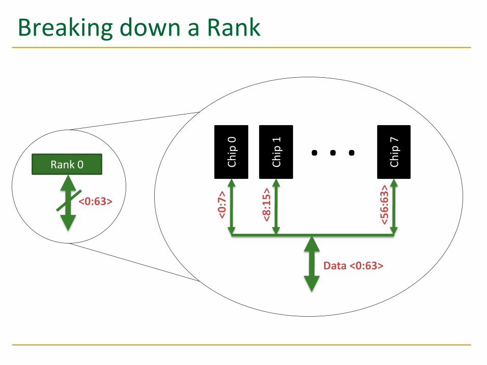
Breaking down a Rank
Rank 0
<0:63>
Ch
ip 0
Ch
ip 1
Ch
ip 7
. . .
<0:7
>
<8:1
5>
<56
:63
>
Data <0:63>

Breaking down a Chip
Ch
ip 0
<0
:7>
Bank 0
<0:7>
<0:7>
<0:7>
...
<0:7
>

Breaking down a Bank
Bank 0
<0:7
>
row 0
row 16k-1
... 2kB
1B
1B (column)
1B
Row-buffer
1B
... <0
:7>

DRAM Subsystem Organization
Channel
DIMM
Rank
Chip
Bank
Row/Column
72

Example: Transferring a cache block
0xFFFF…F
0x00
0x40
...
64B cache block
Physical memory space
Channel 0
DIMM 0
Rank 0
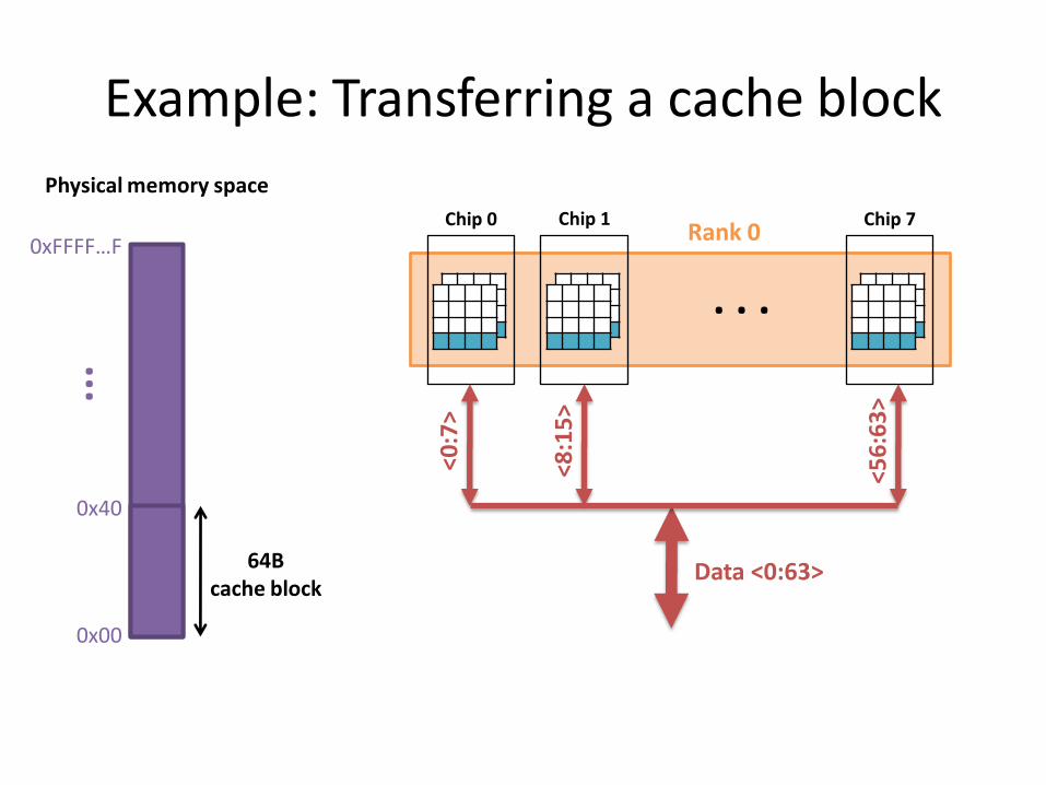
Example: Transferring a cache block
0xFFFF…F
0x00
0x40
...
64B cache block
Physical memory space
Rank 0 Chip 0 Chip 1 Chip 7
<0:7
>
<8:1
5>
<56
:63
>
Data <0:63>
. . .

Example: Transferring a cache block
0xFFFF…F
0x00
0x40
...
64B cache block
Physical memory space
Rank 0 Chip 0 Chip 1 Chip 7
<0:7
>
<8:1
5>
<56
:63
>
Data <0:63>
Row 0 Col 0
. . .

Example: Transferring a cache block
0xFFFF…F
0x00
0x40
...
64B cache block
Physical memory space
Rank 0 Chip 0 Chip 1 Chip 7
<0:7
>
<8:1
5>
<56
:63
>
Data <0:63>
8B
Row 0 Col 0
. . .
8B

Example: Transferring a cache block
0xFFFF…F
0x00
0x40
...
64B cache block
Physical memory space
Rank 0 Chip 0 Chip 1 Chip 7
<0:7
>
<8:1
5>
<56
:63
>
Data <0:63>
8B
Row 0 Col 1
. . .
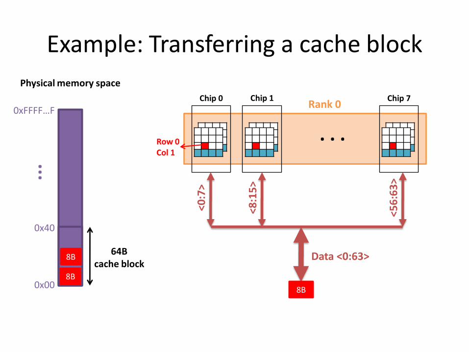
Example: Transferring a cache block
0xFFFF…F
0x00
0x40
...
64B cache block
Physical memory space
Rank 0 Chip 0 Chip 1 Chip 7
<0:7
>
<8:1
5>
<56
:63
>
Data <0:63>
8B
8B
Row 0 Col 1
. . .
8B

Example: Transferring a cache block
0xFFFF…F
0x00
0x40
...
64B cache block
Physical memory space
Rank 0 Chip 0 Chip 1 Chip 7
<0:7
>
<8:1
5>
<56
:63
>
Data <0:63>
8B
8B
Row 0 Col 1
A 64B cache block takes 8 I/O cycles to transfer.
During the process, 8 columns are read sequentially.
. . .

Latency Components: Basic DRAM Operation
CPU → controller transfer time
Controller latency
Queuing & scheduling delay at the controller
Access converted to basic commands
Controller → DRAM transfer time
DRAM bank latency
Simple CAS (column address strobe) if row is “open” OR
RAS (row address strobe) + CAS if array precharged OR
PRE + RAS + CAS (worst case)
DRAM → Controller transfer time
Bus latency (BL)
Controller to CPU transfer time
80
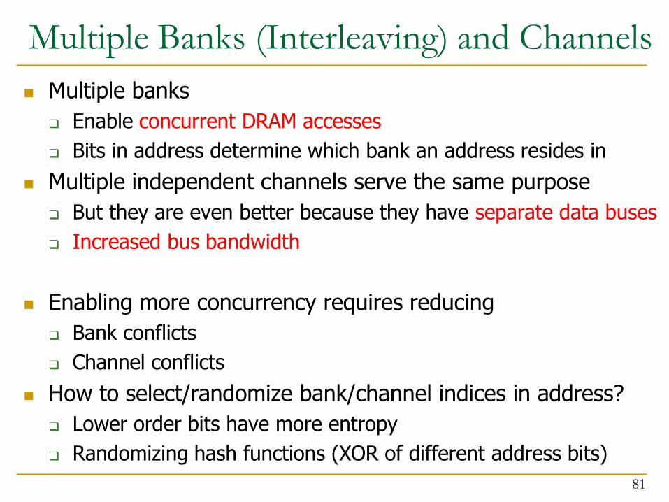
Multiple Banks (Interleaving) and Channels
Multiple banks
Enable concurrent DRAM accesses
Bits in address determine which bank an address resides in
Multiple independent channels serve the same purpose
But they are even better because they have separate data buses
Increased bus bandwidth
Enabling more concurrency requires reducing
Bank conflicts
Channel conflicts
How to select/randomize bank/channel indices in address?
Lower order bits have more entropy
Randomizing hash functions (XOR of different address bits)
81
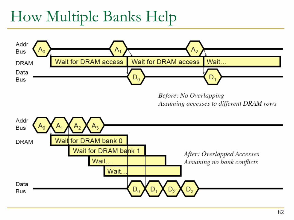
How Multiple Banks Help
82

Address Mapping (Single Channel)
Single-channel system with 8-byte memory bus
2GB memory, 8 banks, 16K rows & 2K columns per bank
Row interleaving
Consecutive rows of memory in consecutive banks
Accesses to consecutive cache blocks serviced in a pipelined manner
Cache block interleaving
Consecutive cache block addresses in consecutive banks
64 byte cache blocks
Accesses to consecutive cache blocks can be serviced in parallel
83
Column (11 bits) Bank (3 bits) Row (14 bits) Byte in bus (3 bits)
Low Col. High Column Row (14 bits) Byte in bus (3 bits) Bank (3 bits)
3 bits 8 bits

Bank Mapping Randomization
DRAM controller can randomize the address mapping to banks so that bank conflicts are less likely
84
Column (11 bits) 3 bits Byte in bus (3 bits)
XOR
Bank index
(3 bits)

Address Mapping (Multiple Channels)
Where are consecutive cache blocks?
85
Column (11 bits) Bank (3 bits) Row (14 bits) Byte in bus (3 bits) C
Column (11 bits) Bank (3 bits) Row (14 bits) Byte in bus (3 bits) C
Column (11 bits) Bank (3 bits) Row (14 bits) Byte in bus (3 bits) C
Column (11 bits) Bank (3 bits) Row (14 bits) Byte in bus (3 bits) C
Low Col. High Column Row (14 bits) Byte in bus (3 bits) Bank (3 bits)
3 bits 8 bits
C
Low Col. High Column Row (14 bits) Byte in bus (3 bits) Bank (3 bits)
3 bits 8 bits
C
Low Col. High Column Row (14 bits) Byte in bus (3 bits) Bank (3 bits)
3 bits 8 bits
C
Low Col. High Column Row (14 bits) Byte in bus (3 bits) Bank (3 bits)
3 bits 8 bits
C
Low Col. High Column Row (14 bits) Byte in bus (3 bits) Bank (3 bits)
3 bits 8 bits
C

Interaction with VirtualPhysical Mapping
Operating System influences where an address maps to in DRAM
Operating system can influence which bank/channel/rank a virtual page is mapped to.
It can perform page coloring to
Minimize bank conflicts
Minimize inter-application interference [Muralidhara+ MICRO’11]
86
Column (11 bits) Bank (3 bits) Row (14 bits) Byte in bus (3 bits)
Page offset (12 bits) Physical Frame number (19 bits)
Page offset (12 bits) Virtual Page number (52 bits) VA
PA
PA

DRAM Refresh (I)
DRAM capacitor charge leaks over time
The memory controller needs to read each row periodically to restore the charge
Activate + precharge each row every N ms
Typical N = 64 ms
Implications on performance?
-- DRAM bank unavailable while refreshed
-- Long pause times: If we refresh all rows in burst, every 64ms the DRAM will be unavailable until refresh ends
Burst refresh: All rows refreshed immediately after one another
Distributed refresh: Each row refreshed at a different time, at regular intervals
87
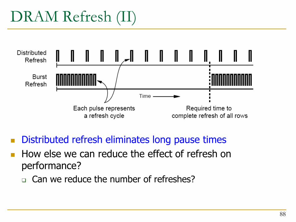
DRAM Refresh (II)
Distributed refresh eliminates long pause times
How else we can reduce the effect of refresh on performance?
Can we reduce the number of refreshes?
88

-- Energy consumption: Each refresh consumes energy
-- Performance degradation: DRAM rank/bank unavailable while refreshed
-- QoS/predictability impact: (Long) pause times during refresh
-- Refresh rate limits DRAM density scaling
Downsides of DRAM Refresh
89
Liu et al., “RAIDR: Retention-aware Intelligent DRAM Refresh,” ISCA 2012.

Memory Controllers

DRAM versus Other Types of Memories
Long latency memories have similar characteristics that need to be controlled.
The following discussion will use DRAM as an example, but many issues are similar in the design of controllers for other types of memories
Flash memory
Other emerging memory technologies
Phase Change Memory
Spin-Transfer Torque Magnetic Memory
91
DRAM Controller: Functions
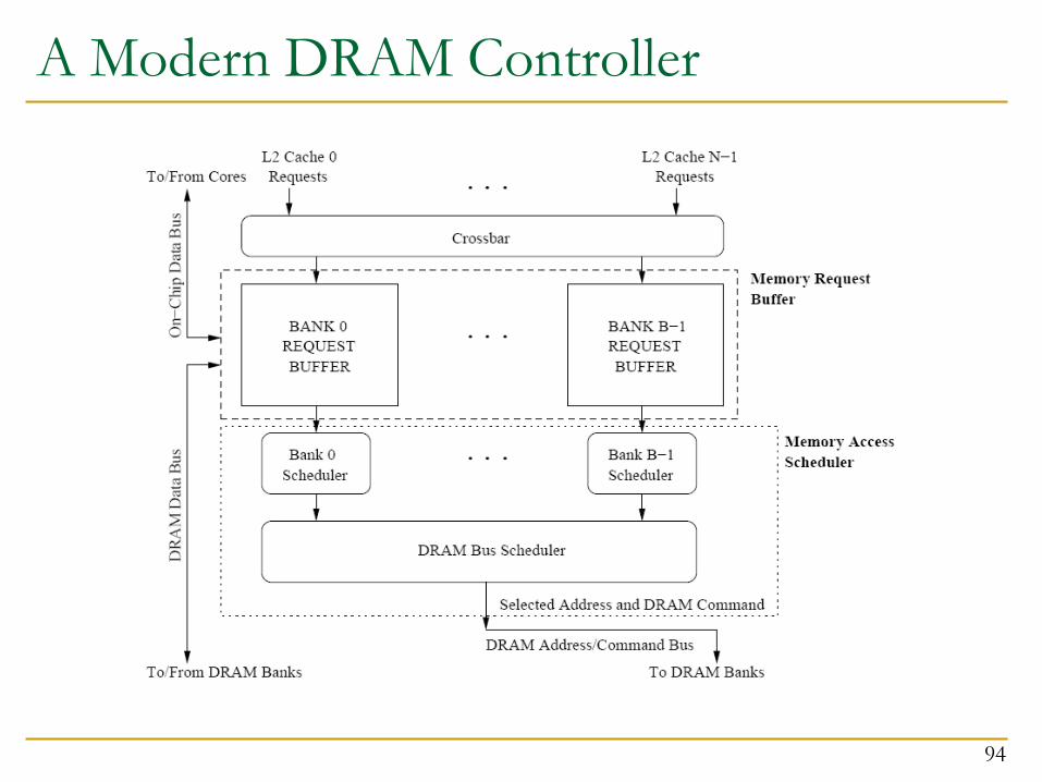
Ensure correct operation of DRAM (refresh and timing)
Service DRAM requests while obeying timing constraints of DRAM chips
Constraints: resource conflicts (bank, bus, channel), minimum write-to-read delays
Translate requests to DRAM command sequences
Buffer and schedule requests to improve performance
Reordering, row-buffer, bank, rank, bus management
Manage power consumption and thermals in DRAM
Turn on/off DRAM chips, manage power modes
92
DRAM Controller: Where to Place
In chipset
+ More flexibility to plug different DRAM types into the system
+ Less power density in the CPU chip
On CPU chip
+ Reduced latency for main memory access
+ Higher bandwidth between cores and controller
More information can be communicated (e.g. request’s importance in the processing core)
93
94
A Modern DRAM Controller
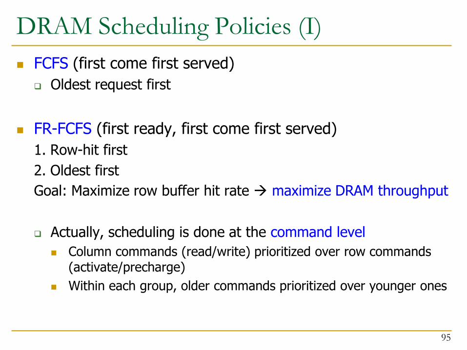
DRAM Scheduling Policies (I)
FCFS (first come first served)
Oldest request first
FR-FCFS (first ready, first come first served)
1. Row-hit first
2. Oldest first
Goal: Maximize row buffer hit rate maximize DRAM throughput
Actually, scheduling is done at the command level
Column commands (read/write) prioritized over row commands (activate/precharge)
Within each group, older commands prioritized over younger ones
95

DRAM Scheduling Policies (II)
A scheduling policy is essentially a prioritization order
Prioritization can be based on
Request age
Row buffer hit/miss status
Request type (prefetch, read, write)
Requestor type (load miss or store miss)
Request criticality
Oldest miss in the core?
How many instructions in core are dependent on it?
96
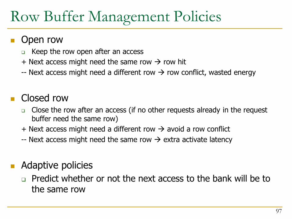
Row Buffer Management Policies
Open row Keep the row open after an access
+ Next access might need the same row row hit
-- Next access might need a different row row conflict, wasted energy
Closed row Close the row after an access (if no other requests already in the request
buffer need the same row)
+ Next access might need a different row avoid a row conflict
-- Next access might need the same row extra activate latency
Adaptive policies
Predict whether or not the next access to the bank will be to the same row
97

Open vs. Closed Row Policies
Policy First access Next access Commands needed for next access
Open row Row 0 Row 0 (row hit) Read
Open row Row 0 Row 1 (row conflict)
Precharge + Activate Row 1 + Read
Closed row Row 0 Row 0 – access in request buffer (row hit)
Read
Closed row Row 0 Row 0 – access not in request buffer (row closed)
Activate Row 0 + Read + Precharge
Closed row Row 0 Row 1 (row closed) Activate Row 1 + Read + Precharge
98
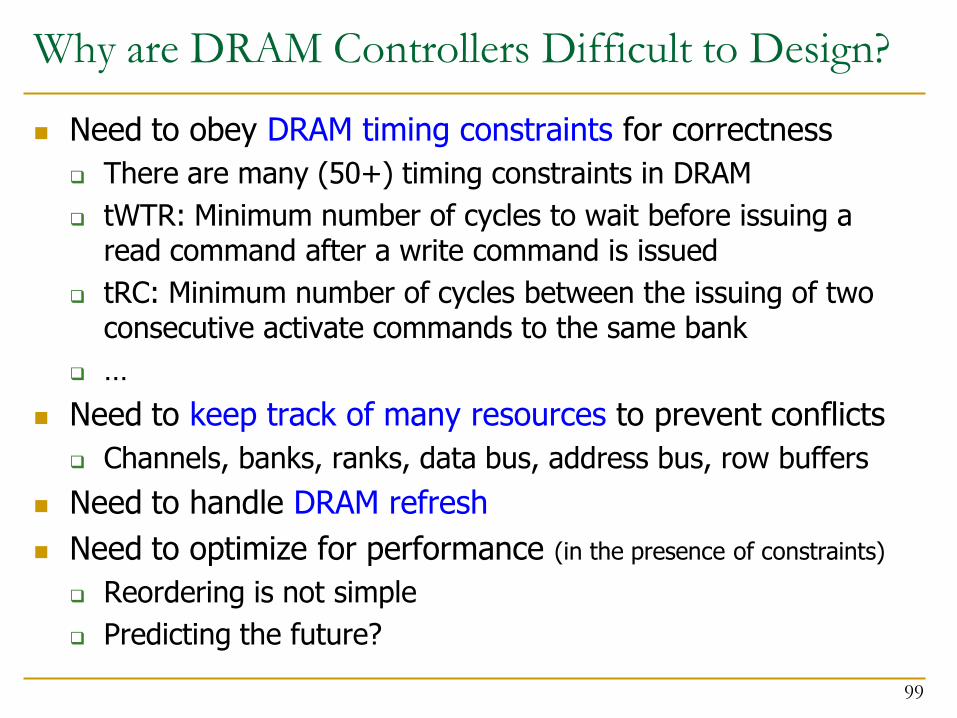
Why are DRAM Controllers Difficult to Design?
Need to obey DRAM timing constraints for correctness
There are many (50+) timing constraints in DRAM
tWTR: Minimum number of cycles to wait before issuing a read command after a write command is issued
tRC: Minimum number of cycles between the issuing of two consecutive activate commands to the same bank
…
Need to keep track of many resources to prevent conflicts
Channels, banks, ranks, data bus, address bus, row buffers
Need to handle DRAM refresh
Need to optimize for performance (in the presence of constraints)
Reordering is not simple
Predicting the future?
99

Many DRAM Timing Constraints
From Lee et al., “DRAM-Aware Last-Level Cache Writeback: Reducing Write-Caused Interference in Memory Systems,” HPS Technical Report, April 2010.
100

More on DRAM Operation
Kim et al., “A Case for Exploiting Subarray-Level Parallelism (SALP) in DRAM,” ISCA 2012.
Lee et al., “Tiered-Latency DRAM: A Low Latency and Low Cost DRAM Architecture,” HPCA 2013.
101

Computer Architecture:
Main Memory (Part I)
Prof. Onur Mutlu
Carnegie Mellon University

We did not cover the remaining slides.

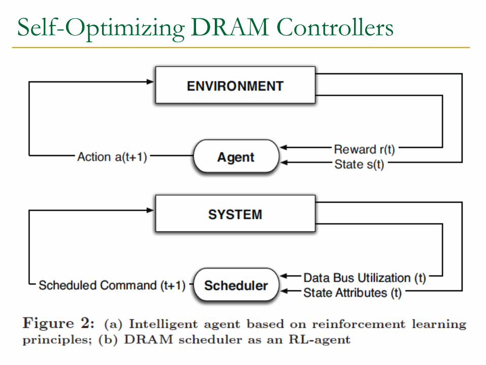
Self-Optimizing DRAM Controllers
Problem: DRAM controllers difficult to design It is difficult for
human designers to design a policy that can adapt itself very well to different workloads and different system conditions
Idea: Design a memory controller that adapts its scheduling policy decisions to workload behavior and system conditions using machine learning.
Observation: Reinforcement learning maps nicely to memory control.
Design: Memory controller is a reinforcement learning agent that dynamically and continuously learns and employs the best scheduling policy.
104
Self-Optimizing DRAM Controllers
Engin Ipek, Onur Mutlu, José F. Martínez, and Rich Caruana, "Self Optimizing Memory Controllers: A Reinforcement Learning Approach" Proceedings of the 35th International Symposium on Computer Architecture (ISCA), pages 39-50, Beijing, China, June 2008.
105

Self-Optimizing DRAM Controllers
Engin Ipek, Onur Mutlu, José F. Martínez, and Rich Caruana, "Self Optimizing Memory Controllers: A Reinforcement Learning Approach" Proceedings of the 35th International Symposium on Computer Architecture (ISCA), pages 39-50, Beijing, China, June 2008.
106

Performance Results
107

DRAM Power Management
DRAM chips have power modes
Idea: When not accessing a chip power it down
Power states
Active (highest power)
All banks idle
Power-down
Self-refresh (lowest power)
Tradeoff: State transitions incur latency during which the chip cannot be accessed
108