Embed Size (px)
Citation preview
Contents
1 The Drude and Sommerfeld models of metals 11.1 What do we know about metals? . . . . . . . . . . . . . . . . . . . . . . . . . . . . . . . 11.2 The Drude model . . . . . . . . . . . . . . . . . . . . . . . . . . . . . . . . . . . . . . . . 2
1.2.1 Assumptions . . . . . . . . . . . . . . . . . . . . . . . . . . . . . . . . . . . . . . 21.2.2 The relaxation-time approximation . . . . . . . . . . . . . . . . . . . . . . . . . . 3
1.3 The failure of the Drude model . . . . . . . . . . . . . . . . . . . . . . . . . . . . . . . . 41.3.1 Electronic heat capacity . . . . . . . . . . . . . . . . . . . . . . . . . . . . . . . . 41.3.2 Thermal conductivity and the Wiedemann-Franz ratio . . . . . . . . . . . . . . . 41.3.3 Hall effect . . . . . . . . . . . . . . . . . . . . . . . . . . . . . . . . . . . . . . . . 61.3.4 Summary . . . . . . . . . . . . . . . . . . . . . . . . . . . . . . . . . . . . . . . . 7
1.4 The Sommerfeld model . . . . . . . . . . . . . . . . . . . . . . . . . . . . . . . . . . . . . 71.4.1 The introduction of quantum mechanics . . . . . . . . . . . . . . . . . . . . . . . 71.4.2 The Fermi-Dirac distribution function. . . . . . . . . . . . . . . . . . . . . . . . . 81.4.3 The electronic density of states . . . . . . . . . . . . . . . . . . . . . . . . . . . . 91.4.4 The electronic density of states at E ≈ EF . . . . . . . . . . . . . . . . . . . . . . 101.4.5 The electronic heat capacity . . . . . . . . . . . . . . . . . . . . . . . . . . . . . . 10
1.5 Successes and failures of the Sommerfeld model . . . . . . . . . . . . . . . . . . . . . . . 121.6 Reading. . . . . . . . . . . . . . . . . . . . . . . . . . . . . . . . . . . . . . . . . . . . . . 13
2 The quantum mechanics of particles in a periodic potential: Bloch’s theorem 152.1 Introduction and health warning . . . . . . . . . . . . . . . . . . . . . . . . . . . . . . . 152.2 Introducing the periodic potential . . . . . . . . . . . . . . . . . . . . . . . . . . . . . . 152.3 Born–von Karman boundary conditions . . . . . . . . . . . . . . . . . . . . . . . . . . . 162.4 The Schrodinger equation in a periodic potential. . . . . . . . . . . . . . . . . . . . . . . 172.5 Bloch’s theorem . . . . . . . . . . . . . . . . . . . . . . . . . . . . . . . . . . . . . . . . . 182.6 Electronic bandstructure. . . . . . . . . . . . . . . . . . . . . . . . . . . . . . . . . . . . 192.7 Reading. . . . . . . . . . . . . . . . . . . . . . . . . . . . . . . . . . . . . . . . . . . . . . 19
3 The nearly-free electron model 213.1 Introduction . . . . . . . . . . . . . . . . . . . . . . . . . . . . . . . . . . . . . . . . . . . 213.2 Dispersion E(k) . . . . . . . . . . . . . . . . . . . . . . . . . . . . . . . . . . . . . . . . 213.3 Nearly free electron model . . . . . . . . . . . . . . . . . . . . . . . . . . . . . . . . . . . 223.4 Consequences of the nearly-free-electron model. . . . . . . . . . . . . . . . . . . . . . . . 22
3.4.1 The alkali metals . . . . . . . . . . . . . . . . . . . . . . . . . . . . . . . . . . . . 233.4.2 Elements with even numbers of valence electrons . . . . . . . . . . . . . . . . . . 233.4.3 More complex Fermi surface shapes . . . . . . . . . . . . . . . . . . . . . . . . . 24
3.5 Reading . . . . . . . . . . . . . . . . . . . . . . . . . . . . . . . . . . . . . . . . . . . . . 25
4 The tight-binding model 274.1 Introduction . . . . . . . . . . . . . . . . . . . . . . . . . . . . . . . . . . . . . . . . . . . 274.2 Band arising from a single electronic level . . . . . . . . . . . . . . . . . . . . . . . . . . 274.3 General points about the formation of tight-binding bands . . . . . . . . . . . . . . . . . 27
4.3.1 An example: the transition metals . . . . . . . . . . . . . . . . . . . . . . . . . . 284.4 Reading . . . . . . . . . . . . . . . . . . . . . . . . . . . . . . . . . . . . . . . . . . . . . 28
i
ii CONTENTS
5 Some general points about bandstructure 315.1 Comparison of tight-binding and nearly-free-electron bandstructure . . . . . . . . . . . . 315.2 The importance of k . . . . . . . . . . . . . . . . . . . . . . . . . . . . . . . . . . . . . . 32
5.2.1 hk is not the momentum . . . . . . . . . . . . . . . . . . . . . . . . . . . . . . . 325.2.2 Group velocity. . . . . . . . . . . . . . . . . . . . . . . . . . . . . . . . . . . . . . 325.2.3 The effective mass . . . . . . . . . . . . . . . . . . . . . . . . . . . . . . . . . . . 325.2.4 The effective mass and the density of states . . . . . . . . . . . . . . . . . . . . . 335.2.5 Summary of the properties of k . . . . . . . . . . . . . . . . . . . . . . . . . . . . 335.2.6 Scattering in the Bloch approach . . . . . . . . . . . . . . . . . . . . . . . . . . . 35
5.3 General (non-isotopic) density of states . . . . . . . . . . . . . . . . . . . . . . . . . . . 355.3.1 Van Hove singularities . . . . . . . . . . . . . . . . . . . . . . . . . . . . . . . . . 36
5.4 Holes . . . . . . . . . . . . . . . . . . . . . . . . . . . . . . . . . . . . . . . . . . . . . . . 365.5 Postscript. . . . . . . . . . . . . . . . . . . . . . . . . . . . . . . . . . . . . . . . . . . . . 375.6 Reading. . . . . . . . . . . . . . . . . . . . . . . . . . . . . . . . . . . . . . . . . . . . . . 37
6 Semiconductors and Insulators 396.1 Bandstructure of Si and Ge . . . . . . . . . . . . . . . . . . . . . . . . . . . . . . . . . . 39
6.1.1 General points . . . . . . . . . . . . . . . . . . . . . . . . . . . . . . . . . . . . . 396.1.2 Heavy and light holes . . . . . . . . . . . . . . . . . . . . . . . . . . . . . . . . . 396.1.3 Optical absorption . . . . . . . . . . . . . . . . . . . . . . . . . . . . . . . . . . . 426.1.4 Constant energy surfaces in the conduction bands of Si and Ge . . . . . . . . . . 42
6.2 Bandstructure of the direct-gap III-V and II-VI semiconductors . . . . . . . . . . . . . . 426.2.1 Introduction . . . . . . . . . . . . . . . . . . . . . . . . . . . . . . . . . . . . . . 426.2.2 General points . . . . . . . . . . . . . . . . . . . . . . . . . . . . . . . . . . . . . 426.2.3 Optical absorption . . . . . . . . . . . . . . . . . . . . . . . . . . . . . . . . . . . 446.2.4 Constant energy surfaces in direct-gap III-V semiconductors . . . . . . . . . . . . 45
6.3 Thermal population of bands in semiconductors . . . . . . . . . . . . . . . . . . . . . . . 456.3.1 The law of Mass-Action . . . . . . . . . . . . . . . . . . . . . . . . . . . . . . . . 456.3.2 The motion of the chemical potential . . . . . . . . . . . . . . . . . . . . . . . . . 476.3.3 Intrinsic carrier density . . . . . . . . . . . . . . . . . . . . . . . . . . . . . . . . 476.3.4 Impurities and extrinsic carriers . . . . . . . . . . . . . . . . . . . . . . . . . . . 476.3.5 Extrinsic carrier density . . . . . . . . . . . . . . . . . . . . . . . . . . . . . . . . 486.3.6 Degenerate semiconductors. . . . . . . . . . . . . . . . . . . . . . . . . . . . . . . 506.3.7 Impurity bands . . . . . . . . . . . . . . . . . . . . . . . . . . . . . . . . . . . . . 506.3.8 Is it a semiconductor or an insulator? . . . . . . . . . . . . . . . . . . . . . . . . 506.3.9 A note on photoconductivity. . . . . . . . . . . . . . . . . . . . . . . . . . . . . . 51
6.4 Reading. . . . . . . . . . . . . . . . . . . . . . . . . . . . . . . . . . . . . . . . . . . . . . 51
7 Bandstructure engineering 537.1 Introduction . . . . . . . . . . . . . . . . . . . . . . . . . . . . . . . . . . . . . . . . . . . 537.2 Semiconductor alloys . . . . . . . . . . . . . . . . . . . . . . . . . . . . . . . . . . . . . . 537.3 Artificial structures . . . . . . . . . . . . . . . . . . . . . . . . . . . . . . . . . . . . . . . 54
7.3.1 Growth of semiconductor multilayers . . . . . . . . . . . . . . . . . . . . . . . . . 547.3.2 Substrate and buffer layer . . . . . . . . . . . . . . . . . . . . . . . . . . . . . . . 557.3.3 Quantum wells . . . . . . . . . . . . . . . . . . . . . . . . . . . . . . . . . . . . . 557.3.4 Optical properties of quantum wells . . . . . . . . . . . . . . . . . . . . . . . . . 567.3.5 Use of quantum wells in opto-electronics . . . . . . . . . . . . . . . . . . . . . . . 577.3.6 Superlattices . . . . . . . . . . . . . . . . . . . . . . . . . . . . . . . . . . . . . . 577.3.7 Heterojunctions and modulation doping . . . . . . . . . . . . . . . . . . . . . . . 597.3.8 The envelope-function approximation . . . . . . . . . . . . . . . . . . . . . . . . 59
8 Carbon nanotubes 618.1 Introduction . . . . . . . . . . . . . . . . . . . . . . . . . . . . . . . . . . . . . . . . . . . 618.2 Reading . . . . . . . . . . . . . . . . . . . . . . . . . . . . . . . . . . . . . . . . . . . . . 618.3 Lecture slides . . . . . . . . . . . . . . . . . . . . . . . . . . . . . . . . . . . . . . . . . . 61

CONTENTS iii
9 Measurement of bandstructure 71
9.1 Introduction . . . . . . . . . . . . . . . . . . . . . . . . . . . . . . . . . . . . . . . . . . . 71
9.2 Lorentz force and orbits . . . . . . . . . . . . . . . . . . . . . . . . . . . . . . . . . . . . 71
9.2.1 General considerations . . . . . . . . . . . . . . . . . . . . . . . . . . . . . . . . . 71
9.2.2 The cyclotron frequency . . . . . . . . . . . . . . . . . . . . . . . . . . . . . . . . 71
9.2.3 Orbits on a Fermi surface . . . . . . . . . . . . . . . . . . . . . . . . . . . . . . . 73
9.3 The introduction of quantum mechanics . . . . . . . . . . . . . . . . . . . . . . . . . . . 73
9.3.1 Landau levels . . . . . . . . . . . . . . . . . . . . . . . . . . . . . . . . . . . . . . 73
9.3.2 Application of Bohr’s correspondence principle to arbitrarily-shaped Fermi sur-faces in a magnetic field . . . . . . . . . . . . . . . . . . . . . . . . . . . . . . . . 76
9.3.3 Quantisation of the orbit area . . . . . . . . . . . . . . . . . . . . . . . . . . . . . 77
9.3.4 The electronic density of states in a magnetic field . . . . . . . . . . . . . . . . . 77
9.4 Quantum oscillatory phenomena . . . . . . . . . . . . . . . . . . . . . . . . . . . . . . . 77
9.4.1 Types of quantum oscillation . . . . . . . . . . . . . . . . . . . . . . . . . . . . . 79
9.4.2 The de Haas–van Alphen effect . . . . . . . . . . . . . . . . . . . . . . . . . . . . 81
9.4.3 Other parameters which can be deduced from quantum oscillations . . . . . . . . 81
9.4.4 Magnetic breakdown . . . . . . . . . . . . . . . . . . . . . . . . . . . . . . . . . . 83
9.5 Cyclotron resonance . . . . . . . . . . . . . . . . . . . . . . . . . . . . . . . . . . . . . . 85
9.5.1 Cyclotron resonance in metals . . . . . . . . . . . . . . . . . . . . . . . . . . . . . 85
9.5.2 Cyclotron resonance in semiconductors . . . . . . . . . . . . . . . . . . . . . . . . 86
9.6 Interband magneto-optics in semiconductors . . . . . . . . . . . . . . . . . . . . . . . . . 87
9.7 Reading . . . . . . . . . . . . . . . . . . . . . . . . . . . . . . . . . . . . . . . . . . . . . 90
10 Transport of heat and electricity in metals and semiconductors 91
10.1 Thermal and electrical conductivity of metals . . . . . . . . . . . . . . . . . . . . . . . . 91
10.1.1 The “Kinetic theory” of electron transport . . . . . . . . . . . . . . . . . . . . . 91
10.1.2 What do τσ and τκ represent? . . . . . . . . . . . . . . . . . . . . . . . . . . . . . 92
10.1.3 Matthiessen’s rule . . . . . . . . . . . . . . . . . . . . . . . . . . . . . . . . . . . 93
10.1.4 Emission and absorption of phonons . . . . . . . . . . . . . . . . . . . . . . . . . 93
10.1.5 What is the characteristic energy of the phonons involved? . . . . . . . . . . . . 94
10.1.6 Electron–phonon scattering at room temperature . . . . . . . . . . . . . . . . . . 94
10.1.7 Electron-phonon scattering at T θD . . . . . . . . . . . . . . . . . . . . . . . . 94
10.1.8 Departures from the low temperature σ ∝ T−5 dependence. . . . . . . . . . . . 95
10.1.9 Very low temperatures and/or very dirty metals . . . . . . . . . . . . . . . . . . 95
10.1.10 Summary . . . . . . . . . . . . . . . . . . . . . . . . . . . . . . . . . . . . . . . . 96
10.1.11 Electron–electron scattering . . . . . . . . . . . . . . . . . . . . . . . . . . . . . . 96
10.2 Electrical conductivity of semiconductors . . . . . . . . . . . . . . . . . . . . . . . . . . 96
10.2.1 Temperature dependence of the carrier densities . . . . . . . . . . . . . . . . . . 96
10.2.2 The temperature dependence of the mobility . . . . . . . . . . . . . . . . . . . . 99
10.3 Reading . . . . . . . . . . . . . . . . . . . . . . . . . . . . . . . . . . . . . . . . . . . . . 99
11 Magnetoresistance in three-dimensional systems 101
11.1 Introduction . . . . . . . . . . . . . . . . . . . . . . . . . . . . . . . . . . . . . . . . . . . 101
11.2 Hall effect with more than one type of carrier . . . . . . . . . . . . . . . . . . . . . . . . 101
11.2.1 General considerations . . . . . . . . . . . . . . . . . . . . . . . . . . . . . . . . . 101
11.2.2 Hall effect in the presence of electrons and holes . . . . . . . . . . . . . . . . . . 102
11.2.3 A clue about the origins of magnetoresistance . . . . . . . . . . . . . . . . . . . . 103
11.3 Magnetoresistance in metals . . . . . . . . . . . . . . . . . . . . . . . . . . . . . . . . . . 103
11.3.1 The absence of magnetoresistance in the Sommerfeld model of metals . . . . . . 103
11.3.2 The presence of magnetoresistance in real metals . . . . . . . . . . . . . . . . . . 105
11.3.3 The use of magnetoresistance in finding the Fermi surface shape . . . . . . . . . 106
11.4 The magnetophonon effect . . . . . . . . . . . . . . . . . . . . . . . . . . . . . . . . . . . 107
11.5 Reading . . . . . . . . . . . . . . . . . . . . . . . . . . . . . . . . . . . . . . . . . . . . . 109
CONTENTS 1
12 Magnetoresistance in two-dimensional systems and the quantum Hall effect 11112.1 Introduction: two dimensional systems . . . . . . . . . . . . . . . . . . . . . . . . . . . . 11112.2 Two-dimensional Landau-level density of states . . . . . . . . . . . . . . . . . . . . . . . 112
12.2.1 Resistivity and conductivity tensors for a two-dimensional system . . . . . . . . 11312.3 Quantisation of the Hall resistivity . . . . . . . . . . . . . . . . . . . . . . . . . . . . . . 114
12.3.1 Localised and extended states . . . . . . . . . . . . . . . . . . . . . . . . . . . . . 11512.3.2 A further refinement– spin splitting . . . . . . . . . . . . . . . . . . . . . . . . . 115
12.4 Summary . . . . . . . . . . . . . . . . . . . . . . . . . . . . . . . . . . . . . . . . . . . . 11612.5 More than one subband populated . . . . . . . . . . . . . . . . . . . . . . . . . . . . . . 11812.6 Reading . . . . . . . . . . . . . . . . . . . . . . . . . . . . . . . . . . . . . . . . . . . . . 118

2 CONTENTS
Handout 1
The Drude and Sommerfeld modelsof metals
This series of lecture notes covers all the material that I will present via transparencies during thispart of the C3 major option. However, thoughout the course the material that I write on theblackboard will not necessarily be covered in this transcript. Therefore I strongly advise youto take good notes on the material that I present on the board. In some cases a different approach toa topic may be presented in these notes – this is designed to help you understand a topic more fully.
I recommend the book Band theory and electronic properties of solids, by John Singleton (OxfordUniversity Press, 2001) as a primary textbook for this part of the course. Dr Singleton lectured thiscourse for a number of years and the book is very good. You should also read other accounts in particularthose in Solid State Physics, by N.W Ashcroft and N.D. Mermin (Holt, Rinehart and Winston, NewYork 1976)and Fundamentals of semiconductors, by P. Yu and M. Cardona (Springer, Berlin, 1996). Youmay also find Introduction to Solid State Physics, by Charles Kittel, seventh edition (Wiley, New York1996) and Solid State Physics, by G. Burns (Academic Press, Boston, 1995) useful. The lecture notesand both problem sets are on the website http://www2.physics.ox.ac.uk/students/course-materials/c3-condensed-matter-major-option. You will find that this first section is mainly revision, but it will getyou ready for the new material in the lectures.
We start the course by examining metals, the class of solids in which the presence of charge-carryingelectrons is most obvious. By discovering why and how metals exhibit high electrical conductivity, wecan, with luck, start to understand why other materials (glass, diamond, wood) do not.
1.1 What do we know about metals?
To understand metals, it is useful to list some of their properties, and contrast them with other classesof solids. I hope that you enjoy the course!
1. The metallic state is favoured by elements; > 23 are metals.
2. Metals tend to come from the left-hand side of the periodic table; therefore, a metal atom willconsist of a rather tightly bound “noble-gas-like” ionic core surrounded by a small number of moreloosely-bound valence electrons.
3. Metals form in crystal structures which have relatively large numbers nnn of nearest neigh-bours, e.g.
hexagonal close-packed nnn = 12;
face-centred cubic nnn = 12
body-centred cubic nnn = 8 at distance d (the nearest-neighbour distance) with another 6 at1.15d.
These figures may be compared with typical ionic and covalent systems in which nnn ∼ 4− 6).
1
2 HANDOUT 1. THE DRUDE AND SOMMERFELD MODELS OF METALS
- ( - )e Z Zc
-e Z
- ( - )e Z Zc
- ( - )e Z Zc
- ( - )e Z Zc
Nucleus
Core electrons
Valence electrons
Nucleus
Core
Conduction electrons
Ionf
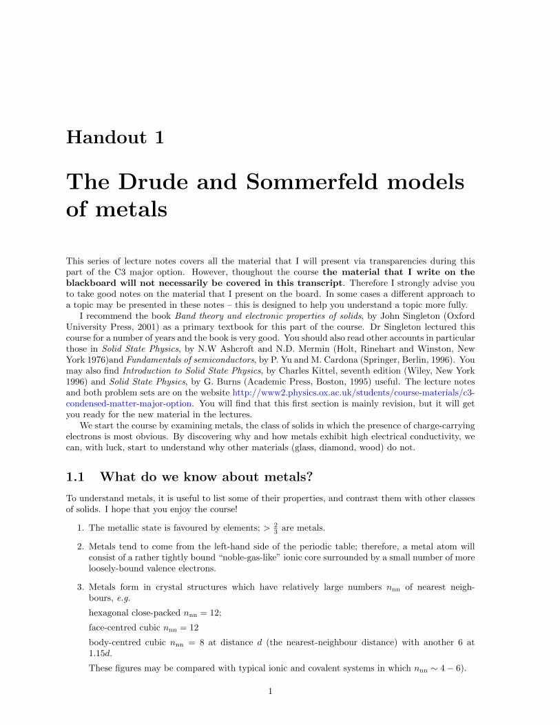
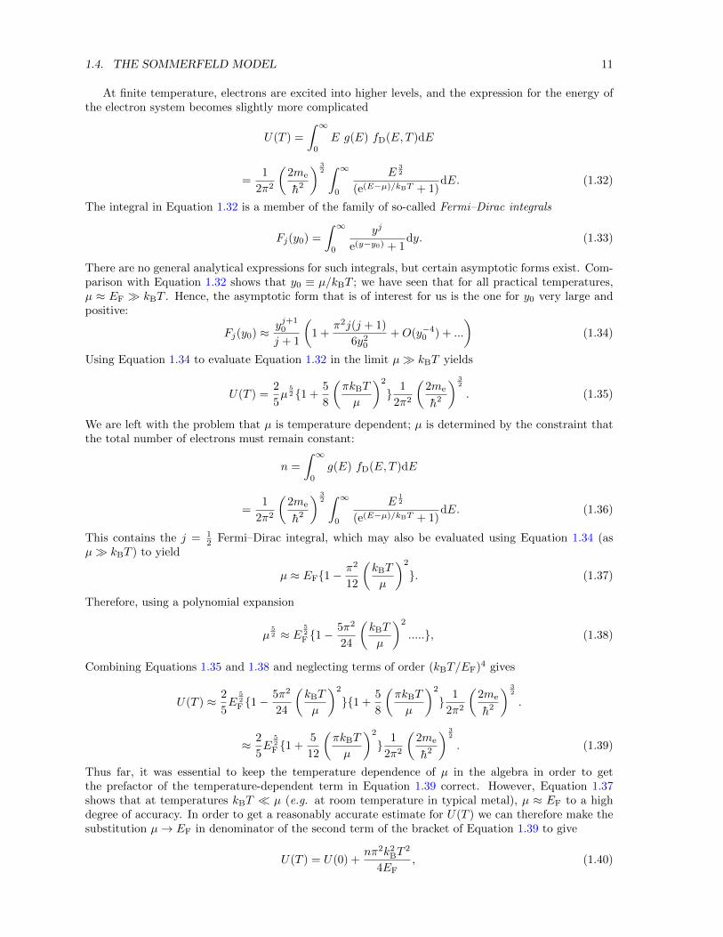
Figure 1.1: Schematic representations of a single, isolated metal atom and a solid metal. The atom(left) consists of a nucleus (size greatly exaggerated!) of charge +eZc surrounded by the core electrons,which provide charge −e(Zc − Z), and Z valence electrons, of charge −eZ. In the solid metal (right),the core electrons remain bound to the nucleus, but the valence electrons move throughout the solid,becoming conduction electrons.
The large coordination numbers and the small numbers of valence electrons (∼ 1) in metals implythat the outer electrons of the metal atoms occupy space between the ionic cores rather uniformly.This suggests the following things.
4. The bonds that bind the metal together are rather undirectional; this is supported by the mal-leability of metals. By contrast, ionic and covalent solids, with their more directional bonds(deduced from the smaller number of nearest neighbours mentioned above) are brittle.
5. There is a lot of “empty space” in metals; e.g. Li has an interatomic distance of 3 A, but the ionicradius is only ∼ 0.5 A. This implies that there is a great deal of volume available for the valence(conduction) electrons to move around in.1
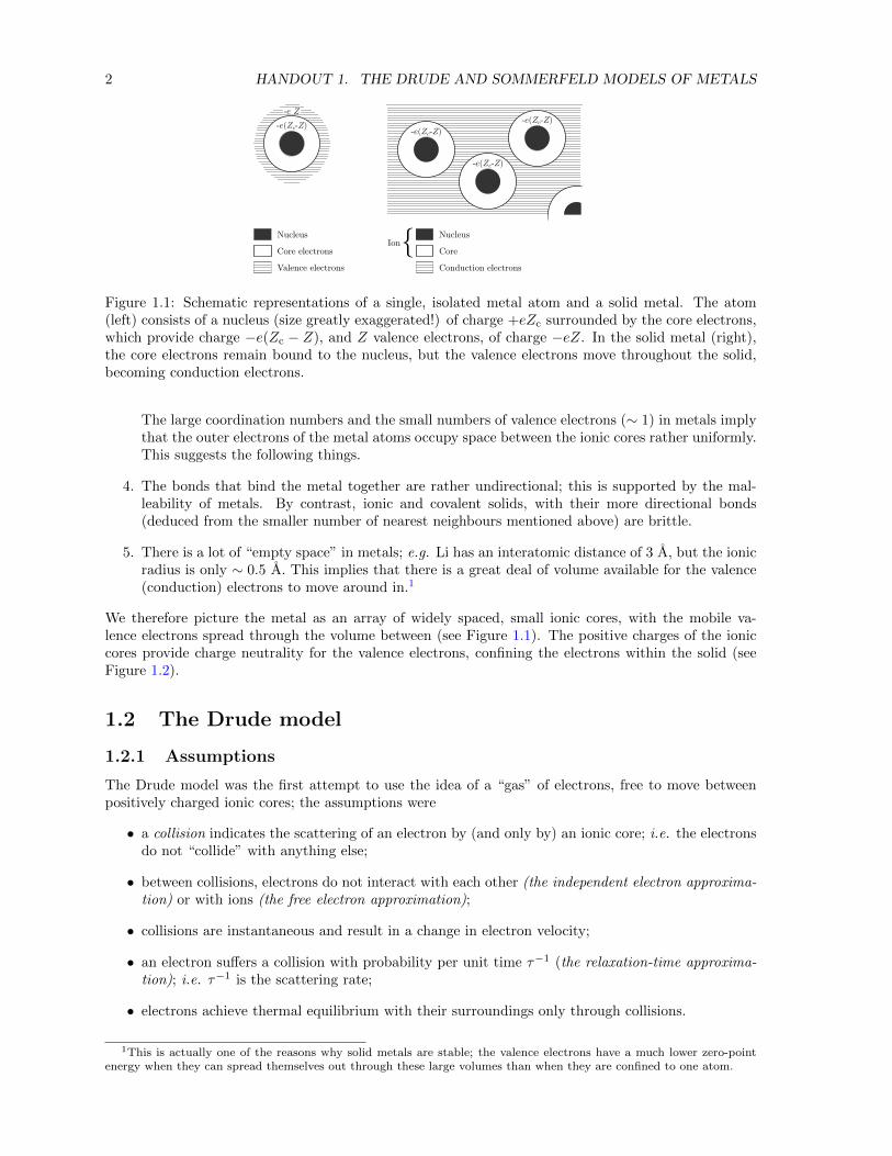
We therefore picture the metal as an array of widely spaced, small ionic cores, with the mobile va-lence electrons spread through the volume between (see Figure 1.1). The positive charges of the ioniccores provide charge neutrality for the valence electrons, confining the electrons within the solid (seeFigure 1.2).
1.2 The Drude model
1.2.1 Assumptions
The Drude model was the first attempt to use the idea of a “gas” of electrons, free to move betweenpositively charged ionic cores; the assumptions were
• a collision indicates the scattering of an electron by (and only by) an ionic core; i.e. the electronsdo not “collide” with anything else;
• between collisions, electrons do not interact with each other (the independent electron approxima-tion) or with ions (the free electron approximation);
• collisions are instantaneous and result in a change in electron velocity;
• an electron suffers a collision with probability per unit time τ−1 (the relaxation-time approxima-tion); i.e. τ−1 is the scattering rate;
• electrons achieve thermal equilibrium with their surroundings only through collisions.
1This is actually one of the reasons why solid metals are stable; the valence electrons have a much lower zero-pointenergy when they can spread themselves out through these large volumes than when they are confined to one atom.
1.2. THE DRUDE MODEL 3
-1
0
(b)(a)
En
erg
y/V
0
Figure 1.2: Schematic of the electronic potential assumed in the Drude and Sommerfeld models ofmetals (a). The small-scale details of the potential due to the ionic cores (shown schematically in (b))are replaced by an average potential −V0. In such a picture, the ionic cores merely maintain chargeneutrality, hence keeping the electrons within the metal; the metal sample acts as a “box” containingelectrons which are free to move within it.
These assumptions should be contrasted with those of the kinetic theory of conventional gases.2 Forexample, in conventional kinetic theory, equilibrium is achieved by collisions between gas molecules; inthe Drude model, the “molecules” (electrons) do not interact with each other at all!
Before discussing the results of the Drude model, we examine how the scattering rate can be includedin the equations of motion of the electrons. This approach will also be useful in more sophisticatedtreatments.
1.2.2 The relaxation-time approximation
The current density J due to electrons is
J = −nev = − neme
p, (1.1)
where me is the electron mass, n is the electron density and p is the average electron momentum.Consider the evolution of p in time δt under the action of an external force f(t). The probability of acollision during δt is δt
τ , i.e. the probability of surviving without colliding is (1− δtτ ). For electrons that
don’t collide, the increase in momentum δp is given by3
δp = f(t)δt+O(δt)2. (1.2)
Therefore, the contribution to the average electron momentum from the electrons that do not collide is
p(t+ δt) = (1− δt
τ)(p(t) + f(t)δt+O(δt)2). (1.3)
Note that the contribution to the average momentum from electrons which have collided will be of order(δt)2 and therefore negligible. This is because they constitute a fraction ∼ δt/τ of the electrons andbecause the momentum that they will have acquired since colliding (each collision effectively randomisestheir momentum) will be ∼ f(t)δt.
Equation 1.3 can then be rearranged to give, in the limit δt→ 0
dp(t)
dt= −p(t)
τ+ f(t). (1.4)
2See e.g. Three phases of matter, by Alan J. Walton, second edition (Clarendon Press, Oxford 1983) Chapters 5-7.3The O(δt)2 comes from the fact that I have allowed the force to vary with time. In other words, the force at time
t+ δt will be slightly different than that at time t; e.g. if δt is very small, then f(t+ δt) ≈ f(t) + (df/dt)δt.
4 HANDOUT 1. THE DRUDE AND SOMMERFELD MODELS OF METALS
In other words, the collisions produce a frictional damping term. This idea will have many applications,even beyond the Drude model; we now use it to derive the electrical conductivity.
The electrical conductivity σ is defined by
J = σE, (1.5)
where E is the electric field. To find σ, we substitute f = −eE into Equation 1.4; we also set dp(t)dt = 0,
as we are looking for a steady-state solution. The momentum can then be substituted into Equation 1.1,to give
σ = ne2τ/me. (1.6)
If we substitute the room-temperature value of σ for a typical metal4 along with a typical n ∼ 1022 −1023cm−3 into this equation, a value of τ ∼ 1− 10 fs emerges. In Drude’s picture, the electrons are theparticles of a classical gas, so that they will possess a mean kinetic energy
1
2me〈v2〉 =
3
2kBT (1.7)
(the brackets 〈 〉 denote the mean value of a quantity). Using this expression to derive a typicalclassical room temperature electron speed, we arrive at a mean free path vτ ∼ 0.1 − 1 nm. This isroughly the same as the interatomic distances in metals, a result consistent with the Drude picture ofelectrons colliding with the ionic cores. However, we shall see later that the Drude model very seriouslyunderestimates typical electronic velocities.
1.3 The failure of the Drude model
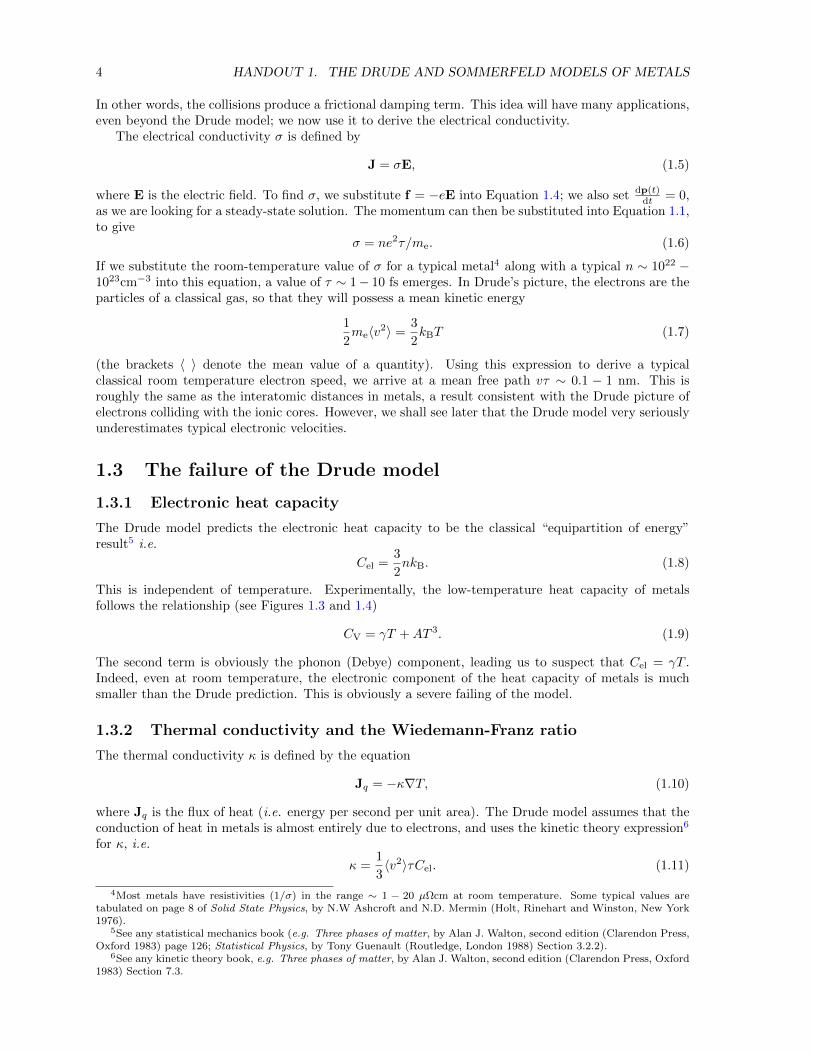
1.3.1 Electronic heat capacity
The Drude model predicts the electronic heat capacity to be the classical “equipartition of energy”result5 i.e.
Cel =3
2nkB. (1.8)
This is independent of temperature. Experimentally, the low-temperature heat capacity of metalsfollows the relationship (see Figures 1.3 and 1.4)
CV = γT +AT 3. (1.9)
The second term is obviously the phonon (Debye) component, leading us to suspect that Cel = γT .Indeed, even at room temperature, the electronic component of the heat capacity of metals is muchsmaller than the Drude prediction. This is obviously a severe failing of the model.
1.3.2 Thermal conductivity and the Wiedemann-Franz ratio
The thermal conductivity κ is defined by the equation
Jq = −κ∇T, (1.10)
where Jq is the flux of heat (i.e. energy per second per unit area). The Drude model assumes that theconduction of heat in metals is almost entirely due to electrons, and uses the kinetic theory expression6
for κ, i.e.
κ =1
3〈v2〉τCel. (1.11)
4Most metals have resistivities (1/σ) in the range ∼ 1 − 20 µΩcm at room temperature. Some typical values aretabulated on page 8 of Solid State Physics, by N.W Ashcroft and N.D. Mermin (Holt, Rinehart and Winston, New York1976).
5See any statistical mechanics book (e.g. Three phases of matter, by Alan J. Walton, second edition (Clarendon Press,Oxford 1983) page 126; Statistical Physics, by Tony Guenault (Routledge, London 1988) Section 3.2.2).
6See any kinetic theory book, e.g. Three phases of matter, by Alan J. Walton, second edition (Clarendon Press, Oxford1983) Section 7.3.

1.3. THE FAILURE OF THE DRUDE MODEL 5
0.2
0.1
00 10 20
T (K)
C(J
mol
K)
-1-1
A
C
B
Figure 1.3: Heat capacity of Co at low temperatures. A is the experimental curve, B is the electroniccontribution γT and C is the Debye component AT 3. (Data from G. Duyckaerts, Physica 6, 817 (1939).)
T2 2
(K )
CT/
(mJ m
olK
)-1
-2 1.6
1.2
0.8
0.4
00 2 4 6 8 10 12 14 1816
Figure 1.4: Plot of CV/T versus T 2 for Cu; the intercept gives γ. (Data from W.S. Corak et al., Phys.Rev. 98, 1699 (1955).)
6 HANDOUT 1. THE DRUDE AND SOMMERFELD MODELS OF METALS
1
0
L L/ 0
Impure
Ideallypure
Temperature
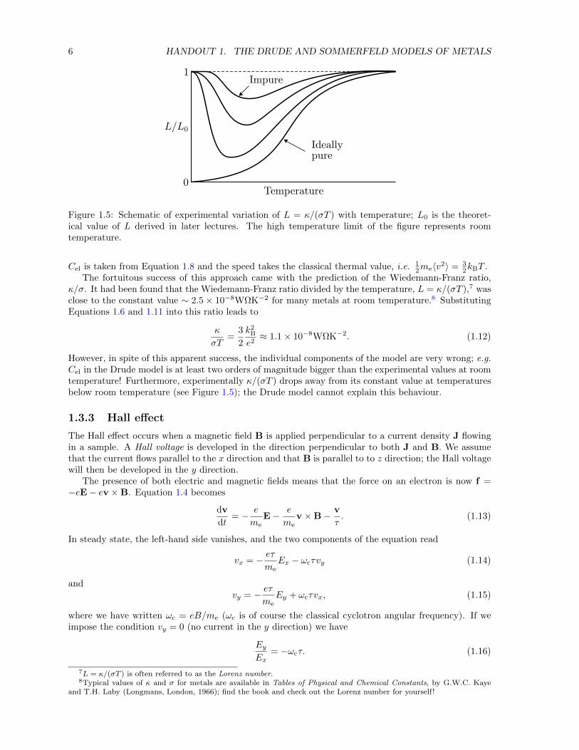
Figure 1.5: Schematic of experimental variation of L = κ/(σT ) with temperature; L0 is the theoret-ical value of L derived in later lectures. The high temperature limit of the figure represents roomtemperature.
Cel is taken from Equation 1.8 and the speed takes the classical thermal value, i.e. 12me〈v2〉 = 3
2kBT .The fortuitous success of this approach came with the prediction of the Wiedemann-Franz ratio,
κ/σ. It had been found that the Wiedemann-Franz ratio divided by the temperature, L = κ/(σT ),7 wasclose to the constant value ∼ 2.5× 10⁻⁸WΩK−2 for many metals at room temperature.8 SubstitutingEquations 1.6 and 1.11 into this ratio leads to
κ
σT=
3
2
k2B
e2≈ 1.1× 10⁻⁸WΩK−2. (1.12)
However, in spite of this apparent success, the individual components of the model are very wrong; e.g.Cel in the Drude model is at least two orders of magnitude bigger than the experimental values at roomtemperature! Furthermore, experimentally κ/(σT ) drops away from its constant value at temperaturesbelow room temperature (see Figure 1.5); the Drude model cannot explain this behaviour.
1.3.3 Hall effect
The Hall effect occurs when a magnetic field B is applied perpendicular to a current density J flowingin a sample. A Hall voltage is developed in the direction perpendicular to both J and B. We assumethat the current flows parallel to the x direction and that B is parallel to to z direction; the Hall voltagewill then be developed in the y direction.
The presence of both electric and magnetic fields means that the force on an electron is now f =−eE− ev ×B. Equation 1.4 becomes
dv
dt= − e
meE− e
mev ×B− v
τ. (1.13)
In steady state, the left-hand side vanishes, and the two components of the equation read
vx = − eτme
Ex − ωcτvy (1.14)
andvy = − eτ
meEy + ωcτvx, (1.15)
where we have written ωc = eB/me (ωc is of course the classical cyclotron angular frequency). If weimpose the condition vy = 0 (no current in the y direction) we have
EyEx
= −ωcτ. (1.16)
7L = κ/(σT ) is often referred to as the Lorenz number.8Typical values of κ and σ for metals are available in Tables of Physical and Chemical Constants, by G.W.C. Kaye
and T.H. Laby (Longmans, London, 1966); find the book and check out the Lorenz number for yourself!
1.4. THE SOMMERFELD MODEL 7
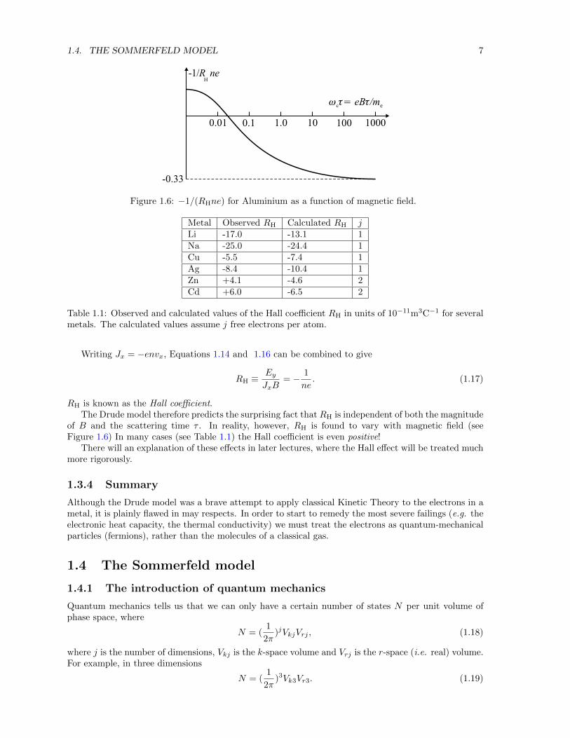
0.01 0.1 1.0 10 100 1000
-0.33
-1/R neH
w t tc
= eB /me
Figure 1.6: −1/(RHne) for Aluminium as a function of magnetic field.
Metal Observed RH Calculated RH jLi -17.0 -13.1 1Na -25.0 -24.4 1Cu -5.5 -7.4 1Ag -8.4 -10.4 1Zn +4.1 -4.6 2Cd +6.0 -6.5 2
Table 1.1: Observed and calculated values of the Hall coefficient RH in units of 10−11m3C−1 for severalmetals. The calculated values assume j free electrons per atom.
Writing Jx = −envx, Equations 1.14 and 1.16 can be combined to give
RH ≡EyJxB
= − 1
ne. (1.17)
RH is known as the Hall coefficient.The Drude model therefore predicts the surprising fact that RH is independent of both the magnitude
of B and the scattering time τ . In reality, however, RH is found to vary with magnetic field (seeFigure 1.6) In many cases (see Table 1.1) the Hall coefficient is even positive!
There will an explanation of these effects in later lectures, where the Hall effect will be treated muchmore rigorously.
1.3.4 Summary
Although the Drude model was a brave attempt to apply classical Kinetic Theory to the electrons in ametal, it is plainly flawed in may respects. In order to start to remedy the most severe failings (e.g. theelectronic heat capacity, the thermal conductivity) we must treat the electrons as quantum-mechanicalparticles (fermions), rather than the molecules of a classical gas.
1.4 The Sommerfeld model
1.4.1 The introduction of quantum mechanics
Quantum mechanics tells us that we can only have a certain number of states N per unit volume ofphase space, where
N = (1
2π)jVkjVrj , (1.18)
where j is the number of dimensions, Vkj is the k-space volume and Vrj is the r-space (i.e. real) volume.For example, in three dimensions
N = (1
2π)3Vk3Vr3. (1.19)

8 HANDOUT 1. THE DRUDE AND SOMMERFELD MODELS OF METALS
Now we assume electrons free to move within the solid; once again we ignore the details of theperiodic potential due to the ionic cores (see Figure 1.2(b)),9 replacing it with a mean potential −V0
(see Figure 1.2(a)). The energy of the electrons is then
E(k) = −V0 +p2
2me= −V0 +
h2k2
2me. (1.20)
However, we are at liberty to set the origin of energy; for convenience we choose E = 0 to correspondto the average potential within the metal (Figure 1.2(a)), so that
E(k) =h2k2
2me. (1.21)
Let us now imagine gradually putting free electrons into a metal. At T = 0, the first electrons willoccupy the lowest energy (i.e. lowest |k|) states; subsequent electrons will be forced to occupy higherand higher energy states (because of Pauli’s Exclusion Principle). Eventually, when all N electrons areaccommodated, we will have filled a sphere of k-space, with
N = 2(1
2π)3 4
3πk3
FVr3, (1.22)
where we have included a factor 2 to cope with the electrons’ spin degeneracy and where kF is thek-space radius (the Fermi wavevector) of the sphere of filled states. Rearranging, remembering thatn = N/Vr3, gives
kF = (3π2n)13 . (1.23)
The corresponding electron energy is
EF =h2k2
F
2me=
h2
2me(3π2n)
23 . (1.24)
This energy is called the Fermi energy.The substitution of typical metallic carrier densities into Equation 1.24,10 produces values of EF
in the range ∼ 1.5 − 15 eV (i.e. ∼ atomic energies) or EF/kB ∼ 20 − 100 × 103 K (i.e. roomtemperature). Typical Fermi wavevectors are kF ∼ 1/(the atomic spacing) ∼ the Brillouin zone size∼ typical X-ray k-vectors. The velocities of electrons at the Fermi surface are vF = hkF/me ∼ 0.01c.Although the Fermi surface is the T = 0 groundstate of the electron system, the electrons present areenormously energetic!
The presence of the Fermi surface has many consequences for the properties of metals; e.g. the maincontribution to the bulk modulus of metals comes from the Fermi “gas” of electrons.11
1.4.2 The Fermi-Dirac distribution function.
In order to treat the thermal properties of electrons at higher temperatures, we need an appropriatedistribution function for electrons from Statistical Mechanics. The Fermi-Dirac distribution function is
fD(E, T ) =1
e(E−µ)/kBT + 1, (1.25)
9Many condensed matter physics texts spend time on hand-waving arguments which supposedly justify the fact thatelectrons do not interact much with the ionic cores. Justifications used include “the ionic cores are very small”; “theelectron–ion interactions are strongest at small separations but the Pauli exclusion principle prevents electrons fromentering this region”; “screening of ionic charge by the mobile valence electrons”; “electrons have higher average kineticenergies whilst traversing the deep ionic potential wells and therefore spend less time there”. We shall see in later lecturesthat it is the translational symmetry of the potential due to the ions which allows the electrons to travel for long distanceswithout scattering from anything.
10Metallic carrier densities are usually in the range ∼ 1022 − 1023cm−3. Values for several metals are tabulated inSolid State Physics, by N.W Ashcroft and N.D. Mermin (Holt, Rinehart and Winston, New York 1976), page 5. See alsoProblem 1.
11See Problem 2; selected bulk moduli for metals have been tabulated on page 39 of Solid State Physics, by N.WAshcroft and N.D. Mermin (Holt, Rinehart and Winston, New York 1976).
1.4. THE SOMMERFELD MODEL 9
f
f
1.0
1.0
(a)
(b)
¹
¹
²
²
(¢ )E k T¼ B
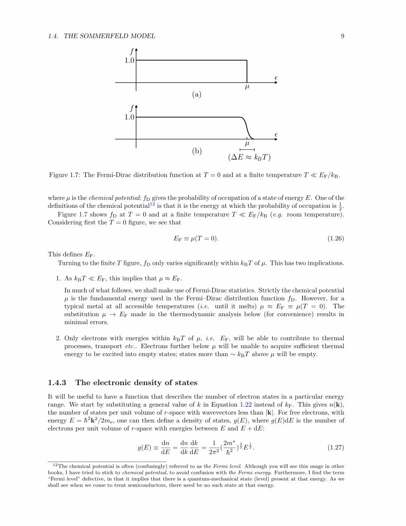
Figure 1.7: The Fermi-Dirac distribution function at T = 0 and at a finite temperature T EF/kB.
where µ is the chemical potential; fD gives the probability of occupation of a state of energy E. One of thedefinitions of the chemical potential12 is that it is the energy at which the probability of occupation is 1
2 .
Figure 1.7 shows fD at T = 0 and at a finite temperature T EF/kB (e.g. room temperature).Considering first the T = 0 figure, we see that
EF ≡ µ(T = 0). (1.26)
This defines EF.
Turning to the finite T figure, fD only varies significantly within kBT of µ. This has two implications.
1. As kBT EF, this implies that µ ≈ EF.
In much of what follows, we shall make use of Fermi-Dirac statistics. Strictly the chemical potentialµ is the fundamental energy used in the Fermi–Dirac distribution function fD. However, for atypical metal at all accessible temperatures (i.e. until it melts) µ ≈ EF ≡ µ(T = 0). Thesubstitution µ → EF made in the thermodynamic analysis below (for convenience) results inminimal errors.
2. Only electrons with energies within kBT of µ, i.e. EF, will be able to contribute to thermalprocesses, transport etc.. Electrons further below µ will be unable to acquire sufficient thermalenergy to be excited into empty states; states more than ∼ kBT above µ will be empty.
1.4.3 The electronic density of states
It will be useful to have a function that describes the number of electron states in a particular energyrange. We start by substituting a general value of k in Equation 1.22 instead of kF. This gives n(k),the number of states per unit volume of r-space with wavevectors less than |k|. For free electrons, withenergy E = h2k2/2me, one can then define a density of states, g(E), where g(E)dE is the number ofelectrons per unit volume of r-space with energies between E and E + dE:
g(E) ≡ dn
dE=
dn
dk
dk
dE=
1
2π2(2m∗
h2 )32E
12 . (1.27)
12The chemical potential is often (confusingly) referred to as the Fermi level. Although you will see this usage in otherbooks, I have tried to stick to chemical potential, to avoid confusion with the Fermi energy. Furthermore, I find the term“Fermi level” defective, in that it implies that there is a quantum-mechanical state (level) present at that energy. As weshall see when we come to treat semiconductors, there need be no such state at that energy.
10 HANDOUT 1. THE DRUDE AND SOMMERFELD MODELS OF METALS
0.2
0.4
0.6
0.8
1.0
2000
10 30 40 50 60 70 80 90 100 110
fMB
f
f
fMB
fFD
x mv k T= /22
B
x mv k T= /22
B
0 1 2 3 4 5 6 7 8 9
100
200
300
400
500
600
700
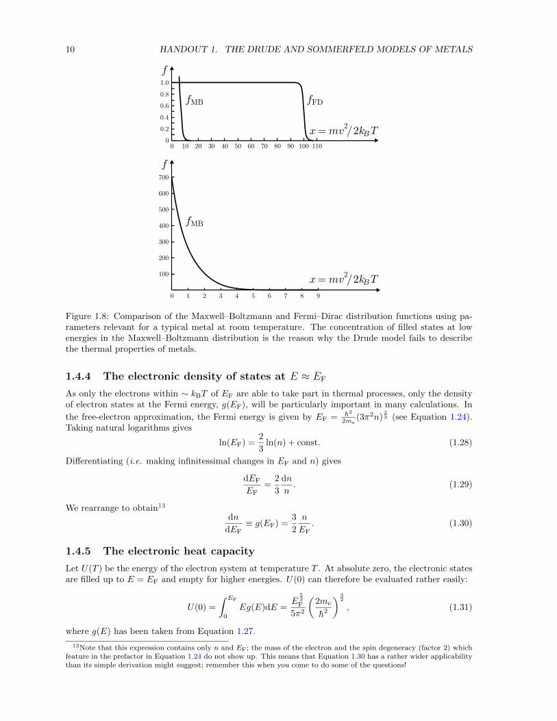
Figure 1.8: Comparison of the Maxwell–Boltzmann and Fermi–Dirac distribution functions using pa-rameters relevant for a typical metal at room temperature. The concentration of filled states at lowenergies in the Maxwell–Boltzmann distribution is the reason why the Drude model fails to describethe thermal properties of metals.
1.4.4 The electronic density of states at E ≈ EF
As only the electrons within ∼ kBT of EF are able to take part in thermal processes, only the densityof electron states at the Fermi energy, g(EF), will be particularly important in many calculations. In
the free-electron approximation, the Fermi energy is given by EF = h2
2me(3π2n)
23 (see Equation 1.24).
Taking natural logarithms gives
ln(EF) =2
3ln(n) + const. (1.28)
Differentiating (i.e. making infinitessimal changes in EF and n) gives
dEF
EF=
2
3
dn
n. (1.29)
We rearrange to obtain13
dn
dEF≡ g(EF) =
3
2
n
EF. (1.30)
1.4.5 The electronic heat capacity
Let U(T ) be the energy of the electron system at temperature T . At absolute zero, the electronic statesare filled up to E = EF and empty for higher energies. U(0) can therefore be evaluated rather easily:
U(0) =
∫ EF
0
Eg(E)dE =E
52
F
5π2
(2me
h2
) 32
, (1.31)
where g(E) has been taken from Equation 1.27.
13Note that this expression contains only n and EF; the mass of the electron and the spin degeneracy (factor 2) whichfeature in the prefactor in Equation 1.24 do not show up. This means that Equation 1.30 has a rather wider applicabilitythan its simple derivation might suggest; remember this when you come to do some of the questions!
1.4. THE SOMMERFELD MODEL 11
At finite temperature, electrons are excited into higher levels, and the expression for the energy ofthe electron system becomes slightly more complicated
U(T ) =
∫ ∞0
E g(E) fD(E, T )dE
=1
2π2
(2me
h2
) 32∫ ∞
0
E32
(e(E−µ)/kBT + 1)dE. (1.32)
The integral in Equation 1.32 is a member of the family of so-called Fermi–Dirac integrals
Fj(y0) =
∫ ∞0
yj
e(y−y0) + 1dy. (1.33)
There are no general analytical expressions for such integrals, but certain asymptotic forms exist. Com-parison with Equation 1.32 shows that y0 ≡ µ/kBT ; we have seen that for all practical temperatures,µ ≈ EF kBT . Hence, the asymptotic form that is of interest for us is the one for y0 very large andpositive:
Fj(y0) ≈ yj+10
j + 1
(1 +
π2j(j + 1)
6y20
+O(y−40 ) + ...
)(1.34)
Using Equation 1.34 to evaluate Equation 1.32 in the limit µ kBT yields
U(T ) =2
5µ
52 1 +
5
8
(πkBT
µ
)2
1
2π2
(2me
h2
) 32
. (1.35)
We are left with the problem that µ is temperature dependent; µ is determined by the constraint thatthe total number of electrons must remain constant:
n =
∫ ∞0
g(E) fD(E, T )dE
=1
2π2
(2me
h2
) 32∫ ∞
0
E12
(e(E−µ)/kBT + 1)dE. (1.36)
This contains the j = 12 Fermi–Dirac integral, which may also be evaluated using Equation 1.34 (as
µ kBT ) to yield
µ ≈ EF1−π2
12
(kBT
µ
)2
. (1.37)
Therefore, using a polynomial expansion
µ52 ≈ E
52
F 1−5π2
24
(kBT
µ
)2
....., (1.38)
Combining Equations 1.35 and 1.38 and neglecting terms of order (kBT/EF)4 gives
U(T ) ≈ 2
5E
52
F 1−5π2
24
(kBT
µ
)2
1 +5
8
(πkBT
µ
)2
1
2π2
(2me
h2
) 32
.
≈ 2
5E
52
F 1 +5
12
(πkBT
µ
)2
1
2π2
(2me
h2
) 32
. (1.39)
Thus far, it was essential to keep the temperature dependence of µ in the algebra in order to getthe prefactor of the temperature-dependent term in Equation 1.39 correct. However, Equation 1.37shows that at temperatures kBT µ (e.g. at room temperature in typical metal), µ ≈ EF to a highdegree of accuracy. In order to get a reasonably accurate estimate for U(T ) we can therefore make thesubstitution µ→ EF in denominator of the second term of the bracket of Equation 1.39 to give
U(T ) = U(0) +nπ2k2
BT2
4EF, (1.40)
12 HANDOUT 1. THE DRUDE AND SOMMERFELD MODELS OF METALS
where we have substituted in the value for U(0) from Equation 1.31. Differentiating, we obtain
Cel ≡∂U
∂T=
1
2π2n
k2BT
EF. (1.41)
Equation 1.41 looks very good as it
1. is proportional to T , as are experimental data (see Figures 1.3 and 1.4);
2. is a factor ∼ kBTEF
smaller than the classical (Drude) value, as are experimental data.
Just in case the algebra of this section has seemed like hard work,14 note that a reasonably accurateestimate of Cel can be obtained using the following reasoning. At all practical temperatures, kBT EF,so that we can say that only the electrons in an energy range ∼ kBT on either side of µ ≈ EF willbe involved in thermal processes. The number density of these electrons will be ∼ kBTg(EF). Eachelectron will be excited to a state ∼ kBT above its groundstate (T = 0) energy. A reasonable estimateof the thermal energy of the system will therefore be
U(T )− U(0) ∼ (kBT )2g(EF) =3
2nkBT
(kBT
EF
),
where I have substituted the value of g(EF) from Equation 1.30. Differentiating with respect to T , weobtain
Cel = 3nkB
(kBT
EF
),
which is within a factor 2 of the more accurate method.
1.5 Successes and failures of the Sommerfeld model
The Sommerfeld model is a great improvement on the Drude model; it can successfully explain
• the temperature dependence and magnitude of Cel;
• the approximate temperature dependence and magnitudes of the thermal and electrical conduc-tivities of metals, and the Wiedemann–Franz ratio (see later lectures);
• the fact that the electronic magnetic susceptibility is temperature independent.15
It cannot explain
• the Hall coefficients of many metals (see Figure 1.6 and Table 1.1; Sommerfeld predicts RH =−1/ne);
• the magnetoresistance exhibited by metals (see subsequent lectures);
• other parameters such as the thermopower;
• the shapes of the Fermi surfaces in many real metals;
• the fact that some materials are insulators and semiconductors (i.e. not metals).
Furthermore, it seems very intellectually unsatisfying to completely disregard the interactions betweenthe electrons and the ionic cores, except as a source of instantaneous “collisions”. This is actuallythe underlying source of the difficulty; to remedy the failures of the Sommerfeld model, we must re-introduce the interactions between the ionic cores and the electrons. In other words, we must introducethe periodic potential of the lattice.
14The method for deriving the electronic heat capacity used in books such as Introduction to Solid State Physics,by Charles Kittel, seventh edition (Wiley, New York 1996) looks at first sight rather simpler than the one that I havefollowed. However, Kittel’s method contains a hidden trap which is not mentioned; it ignores (dµ/dT ), which is said tobe negligible. This term is actually of comparable size to all of the others in Kittel’s integral (see Solid State Physics, byN.W Ashcroft and N.D. Mermin (Holt, Rinehart and Winston, New York 1976) Chapter 2), but happens to disappearbecause of a cunning change of variables. By the time all of this has explained in depth, Kittel’s method looks rathermore tedious and less clear, and I do not blame him for wishing to gloss over the point!
15The susceptibility of metals in the Sommerfeld model is derived in Chapter 7 of Magnetism in Condensed Matter, byS.J. Blundell (OUP 2000).
1.6. READING. 13
1.6 Reading.
A more detailed treatment of the topics in this Chapter is given in Solid State Physics, by N.W Ashcroftand N.D. Mermin (Holt, Rinehart and Winston, New York 1976) Chapters 1-3 and Band theory andelectronic properties of solids, by John Singleton (Oxford University Press, 2001) Chapter 1. Otheruseful information can be found in Electricity and Magnetism, by B.I. Bleaney and B. Bleaney, revisedthird/fourth editions (Oxford University Press, Oxford) Chapter 11, Solid State Physics, by G. Burns(Academic Press, Boston, 1995) Sections 9.1-9.14, Electrons in Metals and Semiconductors, by R.G.Chambers (Chapman and Hall, London 1990) Chapters 1 and 2, and Introduction to Solid State Physics,by Charles Kittel, seventh edition (Wiley, New York 1996) Chapters 6 and 7.

14 HANDOUT 1. THE DRUDE AND SOMMERFELD MODELS OF METALS
Handout 2
The quantum mechanics of particlesin a periodic potential: Bloch’stheorem
2.1 Introduction and health warning
We are going to set up the formalism for dealing with a periodic potential; this is known as Bloch’stheorem. The next two-three lectures are going to appear to be hard work from a conceptual point ofview. However, although the algebra looks complicated, the underlying ideas are really quite simple;you should be able to reproduce the various derivations yourself (make good notes!).
I am going to justify the Bloch theorem fairly rigorously. This formalism will then be used to treattwo opposite limits, a very weak periodic potential and a potential which is so strong that the electronscan hardly move. You will see that both limits give qualitatively similar answers, i.e. reality, which liessomewhere in between, must also be like this!
For this part of the course these notes provide a slightly different (Fourier) approach to the resultsthat I will derive in the lectures. I recommend that you work through and understand both methods,as the Bloch theorem forms the foundation on which the rest of the course is based.
2.2 Introducing the periodic potential
We have been treating the electrons as totally free. We now introduce a periodic potential V (r). Theunderlying translational periodicity of the lattice is defined by the primitive lattice translation vectors
T = n1a1 + n2a2 + n3a3, (2.1)
where n1, n2 and n3 are integers and a1, a2 and a3 are three noncoplanar vectors. 1 Now V (r) mustbe periodic, i.e.
V (r + T) = V (r). (2.2)
The periodic nature of V (r) also implies that the potential may be expressed as a Fourier series
V (r) =∑G
VGeiG.r, (2.3)
where the G are a set of vectors and the VG are Fourier coefficients.2
Equations 2.2 and 2.3 imply that
eiG.T = 1, i .e. G.T = 2pπ, (2.4)
1See Introduction to Solid State Physics, by Charles Kittel, seventh edition (Wiley, New York 1996) pages 4-7.2Notice that the units of G are the same as those of the wavevector k of a particle; |k| = 2π/λ, where λ is the de
Broglie wavelength. The G are vectors in k-space.
15
16HANDOUT 2. THE QUANTUMMECHANICS OF PARTICLES IN A PERIODIC POTENTIAL: BLOCH’S THEOREM
E E
k k0 -2G -G 0 G
Figure 2.1: The effect of introducing the reciprocal lattice; instead of dealing with just one electrondispersion relationship (left) we have an infinite number of copies (right).
where p is an integer. As T = n1a1 + n2a2 + n3a3, this implies that
G = m1A1 +m2A2 +m3A3, (2.5)
where the mj are integers, and the Aj are three noncoplanar vectors defined by
aj .Al = 2πδjl. (2.6)
Take a few moments to convince yourself that this is the only way of defining G which can satisfyEquation 2.4 for all possible T.
Using very simple reasoning, we have shown that the existence of a lattice in r-space automaticallyimplies the existence of a lattice in k-space. The vectors G define the reciprocal lattice; the Aj are itsprimitive translation vectors.
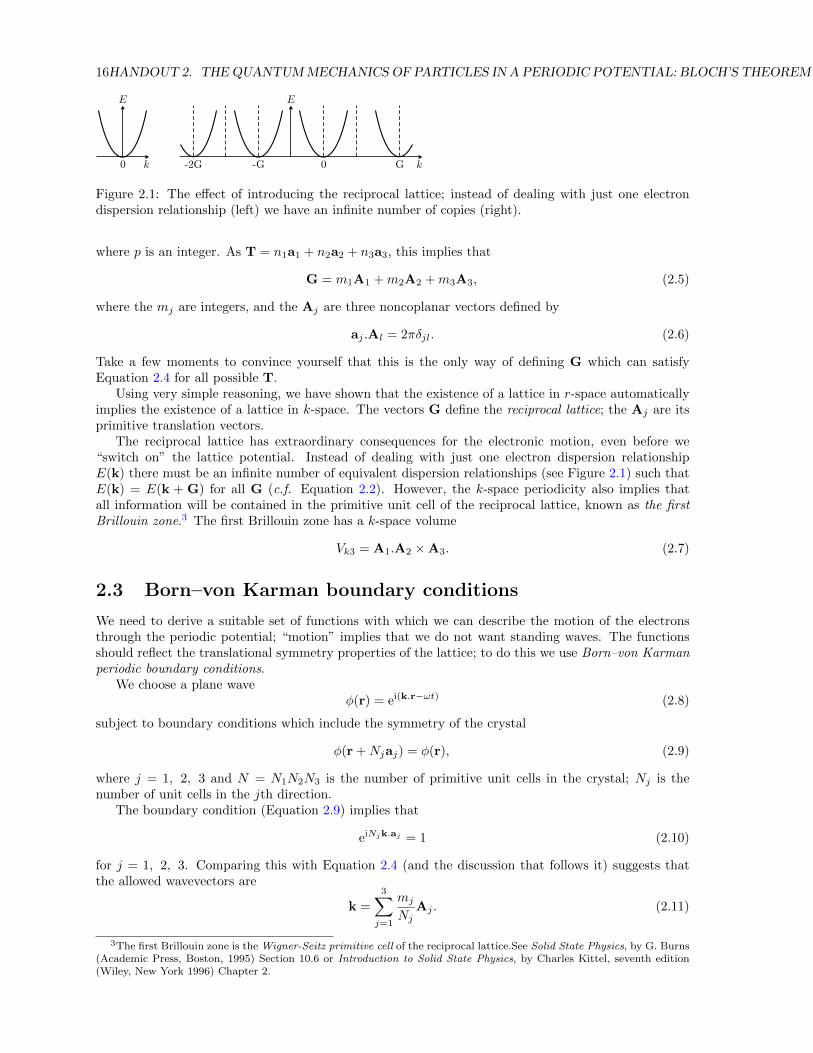
The reciprocal lattice has extraordinary consequences for the electronic motion, even before we“switch on” the lattice potential. Instead of dealing with just one electron dispersion relationshipE(k) there must be an infinite number of equivalent dispersion relationships (see Figure 2.1) such thatE(k) = E(k + G) for all G (c.f. Equation 2.2). However, the k-space periodicity also implies thatall information will be contained in the primitive unit cell of the reciprocal lattice, known as the firstBrillouin zone.3 The first Brillouin zone has a k-space volume
Vk3 = A1.A2 ×A3. (2.7)
2.3 Born–von Karman boundary conditions
We need to derive a suitable set of functions with which we can describe the motion of the electronsthrough the periodic potential; “motion” implies that we do not want standing waves. The functionsshould reflect the translational symmetry properties of the lattice; to do this we use Born–von Karmanperiodic boundary conditions.
We choose a plane waveφ(r) = ei(k.r−ωt) (2.8)
subject to boundary conditions which include the symmetry of the crystal
φ(r +Njaj) = φ(r), (2.9)
where j = 1, 2, 3 and N = N1N2N3 is the number of primitive unit cells in the crystal; Nj is thenumber of unit cells in the jth direction.
The boundary condition (Equation 2.9) implies that
eiNjk.aj = 1 (2.10)
for j = 1, 2, 3. Comparing this with Equation 2.4 (and the discussion that follows it) suggests thatthe allowed wavevectors are
k =
3∑j=1
mj
NjAj . (2.11)
3The first Brillouin zone is the Wigner-Seitz primitive cell of the reciprocal lattice.See Solid State Physics, by G. Burns(Academic Press, Boston, 1995) Section 10.6 or Introduction to Solid State Physics, by Charles Kittel, seventh edition(Wiley, New York 1996) Chapter 2.
2.4. THE SCHRODINGER EQUATION IN A PERIODIC POTENTIAL. 17
Each time that all of the mj change by one we generate a new state; therefore the volume of k-spaceoccupied by one state is
A1
N1.A2
N2× A3
N3=
1
NA1.A2 ×A3. (2.12)
Comparing this with Equation 2.7 shows that the Brillouin zone always contains the same number ofk-states as the number of primitive unit cells in the crystal. This fact will be of immense importancelater on (remember it!); it will be a key factor in determining whether a material is an insulator,semiconductor or metal.
2.4 The Schrodinger equation in a periodic potential.
The Schrodinger equation for a particle4 of mass m in the periodic potential V (r) may be written
Hψ = − h2∇2
2m+ V (r)ψ = Eψ. (2.13)
As before (see Equation 2.3), we write the potential as a Fourier series
V (r) =∑G
VGeiG.r, (2.14)
where the G are the reciprocal lattice vectors. We are at liberty to set the origin of potential energywherever we like; as a convenience for later derivations we set the uniform background potential to bezero, i.e.
V0 ≡ 0. (2.15)
We can write the wavefunction ψ as a sum of plane waves obeying the Born–von Karman boundaryconditions,5
ψ(r) =∑k
Ckeik.r. (2.16)
This ensures that ψ also obeys the Born-von Karman boundary conditions.We now substitute the wavefunction (Equation 2.16) and the potential (Equation 2.14) into the
Schrodinger equation (Equation 2.13) to give∑k
h2k2
2mCkeik.r +
∑G
VGeiG.r∑k
Ckeik.r = E∑k
Ckeik.r. (2.17)
The potential energy term can be rewritten
V (r)ψ =∑G,k
VGCkei(G+k).r, (2.18)
where the sum on the right-hand side is over all G and k. As the sum is over all possible values of Gand k, it can be rewritten as6
V (r)ψ =∑G,k
VGCk−Geik.r. (2.19)
Therefore the Schrodinger equation (Equation 2.17) becomes∑k
eik.r( h2k2
2m− E)Ck +
∑G
VGCk−G = 0. (2.20)
4Note that I have written “a particle”; in the proof of Bloch’s theorem that follows, I do not assume any specific formfor the energy of the particles in the potential. The derivation will be equally true for photons with ω = ck, electronswith E = h2k2/2me etc., etc.. Thus, the conclusions will be seen to be true for any particle in any periodic potential.
5That is, the k in Equation 2.16 are given by Equation 2.11.6Notice that the G also obey the Born–von Karman boundary conditions; this may be easily seen if values of mj that
are integer multiples of Nj are substituted in Equation 2.11. As the sum in Equation 2.16 is over all k that obey theBorn–von Karmann boundary conditions, it automatically encompasses all k−G.
18HANDOUT 2. THE QUANTUMMECHANICS OF PARTICLES IN A PERIODIC POTENTIAL: BLOCH’S THEOREM
As the Born-von Karman plane waves are an orthogonal set of functions, the coefficient of each termin the sum must vanish (one can prove this by multiplying by a plane wave and integrating), i.e.(
h2k2
2m− E
)Ck +
∑G
VGCk−G = 0. (2.21)
(Note that we get the Sommerfeld result if we set VG = 0.)
It is going to be convenient to deal just with solutions in the first Brillouin zone (we have alreadyseen that this contains all useful information about k-space). So, we write k = (q −G′), where q liesin the first Brillouin zone and G′ is a reciprocal lattice vector. Equation 2.21 can then be rewritten(
h2(q−G′)2
2m− E
)Cq−G′ +
∑G
VGCq−G′−G = 0. (2.22)
Finally, we change variables so that G′′ → G + G′, leaving the equation of coefficients in the form(h2(q−G′)2
2m− E
)Cq−G′ +
∑G′′
VG′′−G′Cq−G′′ = 0. (2.23)
This equation of coefficients is very important, in that it specifies the Ck which are used to make upthe wavefunction ψ in Equation 2.16.
2.5 Bloch’s theorem
Equation 2.23 only involves coefficients Ck in which k = q−G, with the G being general reciprocallattice vectors. In other words, if we choose a particular value of q, then the only Ck that feature inEquation 2.23 are of the form Cq−G; these coefficients specify the form that the the wavefunction ψwill take (see Equation 2.16).
Therefore, for each distinct value of q, there is a wavefunction ψq(r) that takes the form
ψq(r) =∑G
Cq−Gei(q−G).r, (2.24)
where we have obtained the equation by substituting k = q−G into Equation 2.16. Equation 2.24 canbe rewritten
ψq(r) = eiq.r∑G
Cq−Ge−iG.r = eiq.ruj,q, (2.25)
i.e. (a plane wave with wavevector within the first Brillouin zone)×(a function uj,q with the periodicityof the lattice).7
This leads us to Bloch’s theorem. “The eigenstates ψ of a one-electron Hamiltonian H = − h2∇2
2m +V (r), where V (r + T) = V (r) for all Bravais lattice translation vectors T can be chosen to be a planewave times a function with the periodicity of the Bravais lattice.”
Note that Bloch’s theorem
• is true for any particle propagating in a lattice (even though Bloch’s theorem is traditionallystated in terms of electron states (as above), in the derivation we made no assumptions aboutwhat the particle was);
• makes no assumptions about the strength of the potential.
7You can check that uj,q (i.e. the sum in Equation 2.25) has the periodicity of the lattice by making the substitutionr→ r + T (see Equations 2.2, 2.3 and 2.4 if stuck).
2.6. ELECTRONIC BANDSTRUCTURE. 19
2.6 Electronic bandstructure.
Equation 2.25 hints at the idea of electronic bandstructure. Each set of uj,q will result in a set of electronstates with a particular character (e.g. whose energies lie on a particular dispersion relationship8); thisis the basis of our idea of an electronic band. The number of possible wavefunctions in this band is justgoing to be given by the number of distinct q, i.e. the number of Born-von Karman wavevectors inthe first Brillouin zone. Therefore the number of electron states in each band is just 2×(the numberof primitive cells in the crystal), where the factor two has come from spin-degeneracy. This is goingto be very important in our ideas about band filling, and the classification of materials into metals,semimetals, semiconductors and insulators.
We are now going to consider two tractable limits of Bloch’s theorem, a very weak periodic potentialand a very strong periodic potential (so strong that the electrons can hardly move from atom to atom).We shall see that both extreme limits give rise to bands, with band gaps between them. In both extremecases, the bands are qualitatively very similar; i.e. real potentials, which must lie somewhere betweenthe two extremes, must also give rise to qualitatively similar bands and band gaps.
2.7 Reading.
This topic is treated with some expansion in Chapter 2 of Band theory and electronic properties ofsolids, by John Singleton (Oxford University Press, 2001). A simple justification of the Bloch theoremis given in Introduction to Solid State Physics, by Charles Kittel, seventh edition (Wiley, New York1996) in the first few pages of Chapter 7 and in Solid State Physics, by G. Burns (Academic Press,Boston, 1995) Section 10.4; an even more elementary one is found in Electricity and Magnetism, byB.I. Bleaney and B. Bleaney, revised third/fourth editions (Oxford University Press, Oxford) Section12.3. More rigorous and general proofs are available in Solid State Physics, by N.W Ashcroft and N.D.Mermin (Holt, Rinehart and Winston, New York 1976) pages 133-140.
8A dispersion relationship is the function E = E(q).

20HANDOUT 2. THE QUANTUMMECHANICS OF PARTICLES IN A PERIODIC POTENTIAL: BLOCH’S THEOREM
Handout 3
The nearly-free electron model
3.1 Introduction
Having derived Bloch’s theorem we are now at a stage where we can start introducing the conceptof bandstructure. When someone refers to the bandstructure of a crystal they are generally talkingabout its electronic dispersion, E(k) (i.e. how the energy of an electron varies as a function of crystalwavevector). However, Bloch’s theorem is very general and can be applied to any periodic interaction,not just to electrons in the periodic electric potential of ions. For example in recent years the power ofband theory has been applied to photons in periodic dielectric media to study photonic bandstructure(i.e. dispersion relations for photons in a “photonic crystal”).
In this lecture we will firstly take a look at dispersion for an electron in a periodic potential wherethe potential very weak (the nearly free electron approximation) and in the next lecture we will lookat the case where the potential is very strong (tight binding approximation). Firstly let’s take a closerlook at dispersion.
3.2 Dispersion E(k)
You will recall from the Sommerfeld model that the dispersion of a free electron is E(k) = h2k2
2m . It iscompletely isotropic (hence the dispersion only depends on k = |k|) and the Sommerfeld model producesexactly this bandstructure for every material – not very exciting! Now we want to understand how thisparabolic relation changes when you consider the periodicity of the lattice.
Using Bloch’s theorem you can show that translational symmetry in real space (characterised bythe set translation vectors T) leads to translational symmetry in k-space (characterised by the set ofreciprocal lattice vectors G). Knowing this we can take another look at Schrodinger’s equation for afree electron in a periodic potential V (r) :
Hψνk(r) = − h2∇2
2m+ V (r)ψνk(r) = Eνkψνk(r). (3.1)
and taking the limit V (r)→ 0 we know that we have a plane wave solution. This implies that the Blochfunction u(r) → 1. However considering the translational invariance in k-space the dispersion relationmust satisfy:
Eνk =h2|k|2
2m=h2|k + G|2
2m(3.2)
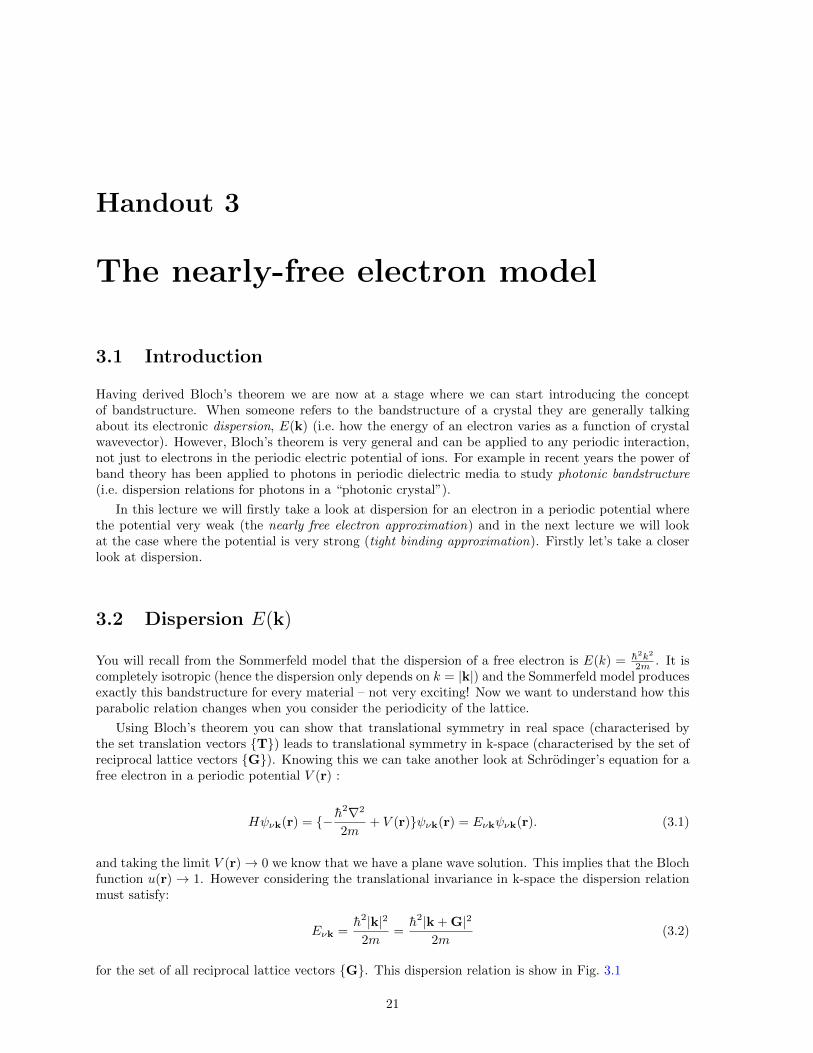
for the set of all reciprocal lattice vectors G. This dispersion relation is show in Fig. 3.1
21
22 HANDOUT 3. THE NEARLY-FREE ELECTRON MODEL
0aπ−3
aπ−2 π
a− π
a aπ2
aπ3 0a
π−3aπ−2 π
a− π
a aπ2
aπ3 π
a− π
a0
E(k) E(k)
kk k
E(k) E(k+G)
G
E(k−G)
(a) (b) (c)
Figure 3.1: Simple bandstructure diagrams for a one dimensional periodic solid in the limit V (r)→ 0expressed in the extended zone (a), repeated zone (b), and reduced zone (c) schemes.
3.3 Nearly free electron model
Since we are in the weak potential limit we can treat the crystal potential as a weak perturbation addedto the Hamiltonian of a free electron. Let’s start with the Schrodinger equation for a free electron
Hoψνk(r) = Eνkψνk(r) (3.3)
where
Ho =p2
2m(3.4)
which has plane wave eigenstates
ψνk(r) =1√Vr3
exp(ik · r) (3.5)
We now introduce a small perturbation, H′ associated with the crystal potential
H = Ho + H′ (3.6)
. Since the lattice is periodic we may expand the perturbation into a Fourier series where G are aset of vectors and VG are Fourier coefficients1
H′ = V (r) =∑G
VG exp(−iG · r). (3.7)
Since the lattice is periodic we may expand the perturbation into a Fourier series where G are a set ofvectors and VG are Fourier coefficients.
...Treating the nearly free electron model using degenerate perturbation theory has been
shown on the blackboard during lectures
3.4 Consequences of the nearly-free-electron model.
In the lectures we have derived two simple rules, which are
• away from Brillouin-zone boundaries the electronic bands (i.e. dispersion relationships) are verysimilar to those of a free electron;
1By considering V (r+Tn) = V (r) you can show that G turns out to be the reciprocal lattice vector (see Section 2.2)
3.4. CONSEQUENCES OF THE NEARLY-FREE-ELECTRON MODEL. 23
• bandgaps open up whenever E(k) surfaces cross, which means in particular at the zone boundaries.
To see how these rules influence the properties of real metals, we must remember that each band inthe Brillouin zone will contain 2N electron states (see Sections 2.3 and 2.6), where N is the number ofprimitive unit cells in the crystal. We now discuss a few specific cases.
3.4.1 The alkali metals
The alkali metals Na, K et al. are monovalent (i.e. have one electron per primitive cell). As a result,their Fermi surfaces, encompassing N states, have a volume which is half that of the first Brillouin zone.Let us examine the geometry of this situation a little more closely.
The alkali metals have a body-centred cubic lattice with a basis comprising a single atom. Theconventional unit cell of the body-centred cubic lattice is a cube of side a containing two lattice points(and hence 2 alkali metal atoms). The electron density is therefore n = 2/a3. Substituting this inthe equation for free-electron Fermi wavevector (Equation 1.23) we find kF = 1.24π/a. The shortestdistance to the Brillouin zone boundary is half the length of one of the Aj for the body-centred cubiclattice, which is
1
2
2π
a(12 + 12 + 02)
12 = 1.41
π
a.
Hence the free-electron Fermi-surface reaches only 1.24/1.41 = 0.88 of the way to the closest Brillouin-zone boundary. The populated electron states therefore have ks which lie well clear of any of theBrillouin-zone boundaries, thus avoiding the distortions of the band due to the bandgaps; hence, thealkali metals have properties which are quite close to the predictions of the Sommerfeld model (e.g. aFermi surface which is spherical to one part in 103).
3.4.2 Elements with even numbers of valence electrons
These substances contain just the right number of electrons (2Np) to completely fill an integer numberp of bands up to a band gap. The gap will energetically separate completely filled states from the nextempty states; to drive a net current through such a system, one must be able to change the velocity ofan electron, i.e move an electron into an unoccupied state of different velocity. However, there are noeasily accessible empty states so that such substances should not conduct electricity at T = 0; at finitetemperatures, electrons will be thermally excited across the gap, leaving filled and empty states in closeenergetic proximity both above and below the gap so that electrical conduction can occur. Diamond(an insulator), Ge and Si (semiconductors) are good examples.
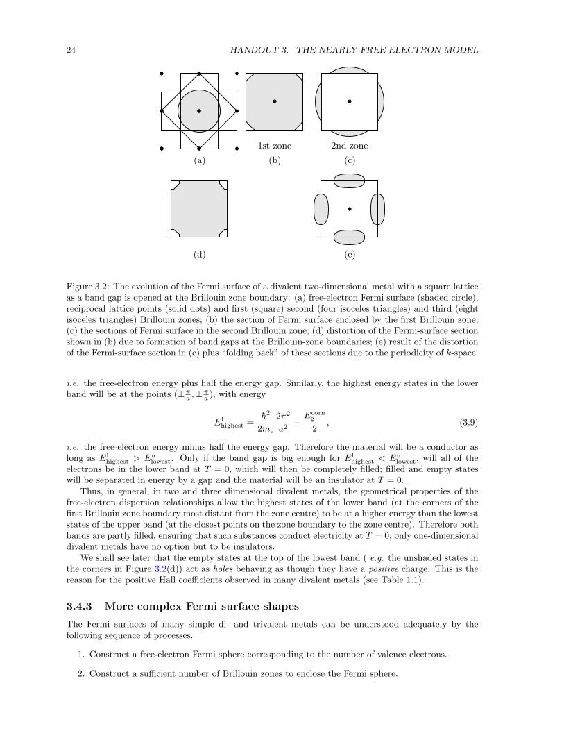
However, the divalent metals Ca et al. plainly conduct electricity rather well. To see why this isthe case, consider the Fermi surface of the two-dimensional divalent metal with a square lattice shownin Figure 3.2. Initially, the free-electron Fermi surface is a circle with an area equivalent to the firstBrillouin zone (Figure 3.2(a)), which consequently straddles the Brillouin-zone boundary (Figures 3.2(b)and (c)). Figures 3.2 (d) and (e) show what happens when a weak periodic potential is “turned on”and bandgaps open up at the Brillouin-zone boundaries; the band gap raises the energy of the statesclose to the zone edge in Figure 3.2(c) and lowers those close to the zone edge in Figure 3.2(b) (seeFigure ??). For ease of reference, we shall call the former states “the upper band” and the latter states“the lower band”. Hence some electrons will transfer back from the upper band (the states above thegap) to the lower band (the states below it), tending to distort the Fermi surface sections close to theBrillouin-zone boundaries.
In the situation shown in Figures 3.2(d) and (e), the material is obviously still an electrical conductor,as filled and empty states are adjacent in energy. Let us call the band gap at the centres of the Brillouin-zone edges Ecent
g and that at the corners of the Brillouin zone Ecorng .2 The lowest energy states in the
upper band will be at points (±πa , 0), (0,±πa ), where a is the lattice parameter of the square lattice,with energy
Eulowest =
h2
2me
π2
a2+Ecent
g
2, (3.8)
2Ecentg and Ecorn
g will in general not be the same; two plane waves contribute to the former and four to the latter.However, the gaps will be of similar magnitude.
24 HANDOUT 3. THE NEARLY-FREE ELECTRON MODEL
Figure 3.2: The evolution of the Fermi surface of a divalent two-dimensional metal with a square latticeas a band gap is opened at the Brillouin zone boundary: (a) free-electron Fermi surface (shaded circle),reciprocal lattice points (solid dots) and first (square) second (four isoceles triangles) and third (eightisoceles triangles) Brillouin zones; (b) the section of Fermi surface enclosed by the first Brillouin zone;(c) the sections of Fermi surface in the second Brillouin zone; (d) distortion of the Fermi-surface sectionshown in (b) due to formation of band gaps at the Brillouin-zone boundaries; (e) result of the distortionof the Fermi-surface section in (c) plus “folding back” of these sections due to the periodicity of k-space.
i.e. the free-electron energy plus half the energy gap. Similarly, the highest energy states in the lowerband will be at the points (±πa ,±
πa ), with energy
Elhighest =
h2
2me
2π2
a2−Ecorn
g
2, (3.9)
i.e. the free-electron energy minus half the energy gap. Therefore the material will be a conductor aslong as El
highest > Eulowest. Only if the band gap is big enough for El
highest < Eulowest, will all of the
electrons be in the lower band at T = 0, which will then be completely filled; filled and empty stateswill be separated in energy by a gap and the material will be an insulator at T = 0.
Thus, in general, in two and three dimensional divalent metals, the geometrical properties of thefree-electron dispersion relationships allow the highest states of the lower band (at the corners of thefirst Brillouin zone boundary most distant from the zone centre) to be at a higher energy than the loweststates of the upper band (at the closest points on the zone boundary to the zone centre). Therefore bothbands are partly filled, ensuring that such substances conduct electricity at T = 0; only one-dimensionaldivalent metals have no option but to be insulators.
We shall see later that the empty states at the top of the lowest band ( e.g. the unshaded states inthe corners in Figure 3.2(d)) act as holes behaving as though they have a positive charge. This is thereason for the positive Hall coefficients observed in many divalent metals (see Table 1.1).
3.4.3 More complex Fermi surface shapes
The Fermi surfaces of many simple di- and trivalent metals can be understood adequately by thefollowing sequence of processes.
1. Construct a free-electron Fermi sphere corresponding to the number of valence electrons.
2. Construct a sufficient number of Brillouin zones to enclose the Fermi sphere.
3.5. READING 25
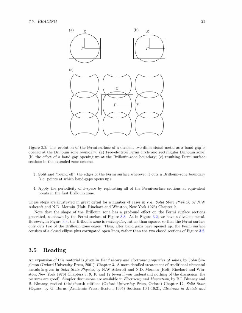
Figure 3.3: The evolution of the Fermi surface of a divalent two-dimensional metal as a band gap isopened at the Brillouin zone boundary. (a) Free-electron Fermi circle and rectangular Brillouin zone;(b) the effect of a band gap opening up at the Brillouin-zone boundary; (c) resulting Fermi surfacesections in the extended-zone scheme.
3. Split and “round off” the edges of the Fermi surface wherever it cuts a Brillouin-zone boundary(i.e. points at which band-gaps opens up).
4. Apply the periodicity of k-space by replicating all of the Fermi-surface sections at equivalentpoints in the first Brillouin zone.
These steps are illustrated in great detail for a number of cases in e.g. Solid State Physics, by N.WAshcroft and N.D. Mermin (Holt, Rinehart and Winston, New York 1976) Chapter 9.
Note that the shape of the Brillouin zone has a profound effect on the Fermi surface sectionsgenerated, as shown by the Fermi surface of Figure 3.3. As in Figure 3.2, we have a divalent metal.However, in Figure 3.3, the Brillouin zone is rectangular, rather than square, so that the Fermi surfaceonly cuts two of the Brillouin zone edges. Thus, after band gaps have opened up, the Fermi surfaceconsists of a closed ellipse plus corrugated open lines, rather than the two closed sections of Figure 3.2.
3.5 Reading
An expansion of this material is given in Band theory and electronic properties of solids, by John Sin-gleton (Oxford University Press, 2001), Chapter 3. A more detailed treatement of traditional elementalmetals is given in Solid State Physics, by N.W Ashcroft and N.D. Mermin (Holt, Rinehart and Win-ston, New York 1976) Chapters 8, 9, 10 and 12 (even if you understand nothing of the discussion, thepictures are good). Simpler discussions are available in Electricity and Magnetism, by B.I. Bleaney andB. Bleaney, revised third/fourth editions (Oxford University Press, Oxford) Chapter 12, Solid StatePhysics, by G. Burns (Academic Press, Boston, 1995) Sections 10.1-10.21, Electrons in Metals and

26 HANDOUT 3. THE NEARLY-FREE ELECTRON MODEL
Semiconductors, by R.G. Chambers (Chapman and Hall, London 1990) Chapters 4-6, Introduction toSolid State Physics, by Charles Kittel, seventh edition (Wiley, New York 1996) Chapters 8 and 9.
Handout 4
The tight-binding model
4.1 Introduction
In the tight-binding model we assume the opposite limit to that used for the nearly-free-electron ap-proach, i.e. the potential is so large that the electrons spend most of their lives bound to ionic cores,only occasionally summoning the quantum-mechanical wherewithal to jump from atom to atom.
The atomic wavefunctions φj(r) are defined by
Hatφj(r) = Ejφj(r), (4.1)
where Hat is the Hamiltonian of a single atom.The assumptions of the model are
1. close to each lattice point, the crystal Hamiltonian H can be approximated by Hat;
2. the bound levels of Hat are well localised, i.e. the φj(r) are very small one lattice spacing away,implying that
3. φj(r) is quite a good approximation to a stationary state of the crystal, as will be φj(r + T).
Reassured by the second and third assumptions, we make the Bloch functions ψj,k of the electrons inthe crystal from linear combinations of the atomic wavefunctions.
4.2 Band arising from a single electronic level
A method of obtaining the dispersion relation for a single electronic level Eν(k) in the tight bindingapproximation was given in lectures. Note that this topic is also covered in a number of textbooks. Bandtheory and electronic properties of solids, by John Singleton (Oxford University Press, 2001) considersthe specific case of a crystal with mutually perpendicular (Cartesian) basis vectors, this may help youunderstand the more general result.
4.3 General points about the formation of tight-binding bands
The derivation given in the lecture illustrates several points about real bandstructure.
1. Figure 4.1 shows schematically the process involved in forming the tight-binding bands. N singleatoms with p (doubly degenerate) atomic levels have become p 2N -fold degenerate bands.
2. The transfer integrals give a direct measure of the width in energy of a band (the bandwidth);small transfer integrals will give a narrow bandwidth. In question 2 of problem set 1, we shallsee that carriers close to the bottom of a tight-binding band have effective masses which areinversely proportional to the transfer integrals. The effective mass parameterises the ease with
27
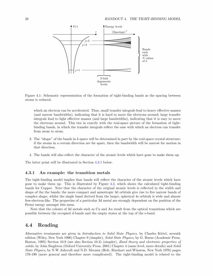
28 HANDOUT 4. THE TIGHT-BINDING MODEL
N-folddegenerate
levels
<
;
;
Bandseachwith
valuesofN
k
V r( )
j=3
j=2
j=1
r
Energy levels
(Spacings)-1
n
Figure 4.1: Schematic representation of the formation of tight-binding bands as the spacing betweenatoms is reduced.
which an electron can be accelerated. Thus, small transfer integrals lead to heavy effective masses(and narrow bandwidths), indicating that it is hard to move the electrons around; large transferintegrals lead to light effective masses (and large bandwidths), indicating that it is easy to movethe electrons around. This ties in exactly with the real-space picture of the formation of tight-binding bands, in which the transfer integrals reflect the ease with which an electron can transferfrom atom to atom.
3. The “shape” of the bands in k-space will be determined in part by the real-space crystal structure;if the atoms in a certain direction are far apart, then the bandwidth will be narrow for motion inthat direction.
4. The bands will also reflect the character of the atomic levels which have gone to make them up.
The latter point will be illustrated in Section 4.3.1 below.
4.3.1 An example: the transition metals
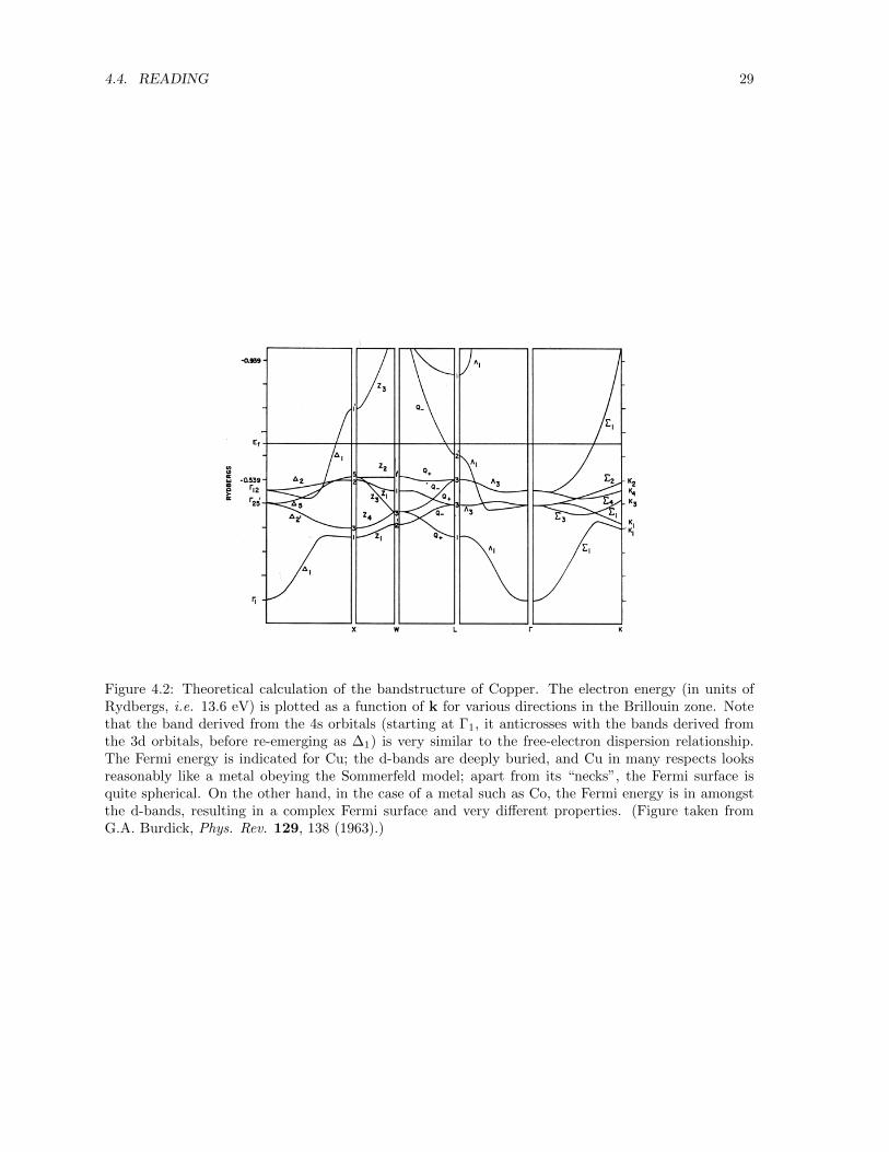
The tight-binding model implies that bands will reflect the character of the atomic levels which havegone to make them up. This is illustrated by Figure 4.2, which shows the calculated tight-bindingbands for Copper. Note that the character of the original atomic levels is reflected in the width andshape of the the bands; the more compact and anisotropic 3d orbitals give rise to five narrow bands ofcomplex shape, whilst the single band derived from the larger, spherical 4s orbitals is wide and almostfree-electron-like. The properties of a particular 3d metal are strongly dependent on the position of theFermi energy amongst this mess.
Note that the colours of 3d metals such as Cu and Au result from the optical transitions which arepossible between the occupied d-bands and the empty states at the top of the s-band.
4.4 Reading
Alternative treatments are given in Introduction to Solid State Physics, by Charles Kittel, seventhedition (Wiley, New York 1996) Chapter 9 (simpler), Solid State Physics, by G. Burns (Academic Press,Boston, 1995) Section 10.9 (see also Section 10.3) (simpler), Band theory and electronic properties ofsolids, by John Singleton (Oxford University Press, 2001) Chapter 4 (same level, more details) and SolidState Physics, by N.W Ashcroft and N.D. Mermin (Holt, Rinehart and Winston, New York 1976) pages176-190 (more general and therefore more complicated). The tight-binding model is related to the
4.4. READING 29
Figure 4.2: Theoretical calculation of the bandstructure of Copper. The electron energy (in units ofRydbergs, i.e. 13.6 eV) is plotted as a function of k for various directions in the Brillouin zone. Notethat the band derived from the 4s orbitals (starting at Γ1, it anticrosses with the bands derived fromthe 3d orbitals, before re-emerging as ∆1) is very similar to the free-electron dispersion relationship.The Fermi energy is indicated for Cu; the d-bands are deeply buried, and Cu in many respects looksreasonably like a metal obeying the Sommerfeld model; apart from its “necks”, the Fermi surface isquite spherical. On the other hand, in the case of a metal such as Co, the Fermi energy is in amongstthe d-bands, resulting in a complex Fermi surface and very different properties. (Figure taken fromG.A. Burdick, Phys. Rev. 129, 138 (1963).)

30 HANDOUT 4. THE TIGHT-BINDING MODEL
Kronig-Penney Model, which is a very simple illustration of the formation of bands; see e.g. QuantumMechanics, by Stephen Gasiorowicz (Wiley, New York 1974) page 98.
Handout 5
Some general points aboutbandstructure
5.1 Comparison of tight-binding and nearly-free-electronbandstructure
Let us compare a band of the nearly-free-electron model with a one-dimensional tight-binding band
E(k) = E0 − 2t cos(ka), (5.1)
where E0 is a constant. Note that
• both bands look qualitatively similar, i.e.
• both bands have minima and maxima (i.e. points where dE/dk = 0) at the Brillouin-zone centresand boundaries respectively;
• both bands have the same k-space periodicity;
• the tops and bottoms of both bands are approximately parabolic (i.e. E is proportional to (k−k0)2
plus a constant, where k0 is the point in k-space at which the band extremum occurs).
The last point is obvious for the bottom of the lowest nearly-free-electron band. To see that the samething happens for the tight-binding approach, we use the approximation
cos(ka) ≈ 1− (ka)2
2(5.2)
for small ka in Equation 5.1 to give
E(k) ≈ E0 − 2t+ ta2k2. (5.3)
The equivalent proof for the top of the band (close to π/a) is left to the reader.
The above discussion shows that both very weak and very strong periodic potentials give rise toqualitatively similar bands. We therefore expect that our ideas about bands derived from these simplemodels will apply to the real bands in solids, where the potential strengths will fall between the twoextremes. The more complex arrangements of atoms and/or molecules often found in real solids willgive rise to more complex bandshapes, but qualitatively the properties of the bands will be the sameas those of our simple models.
31
32 HANDOUT 5. SOME GENERAL POINTS ABOUT BANDSTRUCTURE
5.2 The importance of k
5.2.1 hk is not the momentum
Bloch’s theorem has introduced wavevectors which we have labelled k and q (see e.g. Equation 2.25).Although at first sight k and q look similar to the straightforward electron momentum p = hk in theSommerfeld model, it is easy to show that the Bloch functions are not eigenstates of the momentumoperator;
h
i∇ψ(r) =
h
i∇eiq.ruj,q = hqψ(r) + eiq.r
h
i∇uj,q 6= pψ(r) (5.4)
(where the Bloch wavefunction used is defined in Equation 2.25).The quantity hk is instead a crystal momentum, the momentum of the system as a whole; it is
better to think of k as a quantum number which describes a Bloch state.
5.2.2 Group velocity.
In the original formulation of the Bloch states (see Equation 2.16), the electron wavefunction was definedto be the superposition of a set of plane waves (a wavepacket). It is therefore possible to use the ideaof a group velocity v
v =1
h∇kE, (5.5)
where ∇k is the gradient operator in k-space, to describe the real-space motion of the electron (c.f.v = (dω/dk) for the wavepackets encountered in Optics). Bearing this in mind, we are now going toderive the effective mass, which is very useful in parameterising the dynamics of band electrons whenthey are subjected to external forces. The derivation also illustrates a very important point about k. Ishall follow the derivation through in one dimension; one of the problems involves doing the same thingin three dimensions.
5.2.3 The effective mass
Let an external force f be applied to a band electron. The force will do work
δE = fvδt (5.6)
in time δt. In addition,
δE =dE
dkδk = hvδk. (5.7)
Equating Equations 5.6 and 5.7, dividing through by δt and considering the limit δt→ 0 gives
hdk
dt= f. (5.8)
The equivalent three dimensional formula in the derivation of one of the problems is
hdk
dt= f , (5.9)
where k and f are now vectors. Equation 5.9 is enormously important; it shows that in a crystal hdkdt
is equal to the external force on the electron.After this amazing fact, the rest of the effective mass derivation is almost an anticlimax. The rate
of change of velocity with time isdv
dt=
1
h
d2E
dkdt=
1
h
d2E
dk2
dk
dt. (5.10)
Substituting for dkdt from Equation 5.8 and rearranging gives
h2
d2Edk2
dv
dt= m∗
dv
dt= f, (5.11)
5.2. THE IMPORTANCE OF K 33
where the effective mass m∗ is defined by
m∗ =h2
d2Edk2
. (5.12)
(The equivalent tensor quantities for an anisotropic band are given in one of the problems.)Equation 5.11 shows that the effective mass gives a convenient way of describing the motion of band
electrons subjected to an external force; the identity “force=(mass×acceleration)” can be used with theeffective mass substituted for the inertial mass.
In general, the effective mass will be energy-dependent. However, one often has to deal with almostempty or almost full bands, i.e. the states close to the minima and maxima of the Ej(k) dispersionrelationships. As we have already seen in Section 5.1, these regions are often approximately parabolic(this is actually a general property of any maximum or minimum– try expanding any function possessingsuch an extremum close to that point using a Taylor series). Close to these points, the electrons cantherefore be treated as if they were free, but with an effective mass; i.e. their dispersion relationship is
E(k) ≈ E0 +h2
2m∗(k− k0)2, (5.13)
where energy E0 and wavevector k0 define the band extremum. Note that m∗ can be either positiveor negative. This approximation often simplifies calculations; m∗ in effect contains all of the necessaryinformation about the way in which the electron’s motion is modified by the crystal potential throughwhich it moves. The equivalent model for anisotropic band extrema is explored in the problem aboutthe effective mass tensor.
5.2.4 The effective mass and the density of states
In the previous lectures, we have seen that it is most natural to count electron states by evaluatingthe volume of k-space occupied (e.g. the Brillouin-zone volume determines the number of electronsthat a band can accommodate). The counting of states is easy, because the states are spread throughphase-space uniformly. However, when one comes to consider the evaluation of quantities such as theelectronic heat capacity, where thermal population of states is a significant factor, it is often convenientto work in terms of energy (see e.g. the derivation of the electronic heat capacity within the Sommerfeldmodel), requiring a knowledge of the number of states per unit energy range per unit volume, g(E).
If one substitutes a general value of k in Equation 1.22 instead of kF, one obtains n(k), the numberof states per unit volume of r-space with wavevectors less than |k|. If the band in question is assumedto obey Equation 5.13 close to the region of interest (i.e. it is parabolic and isotropic), then
g(E) ≡ dn
dE=
dn
dk
dk
dE=
1
2π2(2m∗
h2 )32 (E − E0)
12 . (5.14)
This shows that the effective mass is a very convenient way of parameterising the curvature of a bandat a certain energy, and hence the density of states g(E) at that energy. We shall use this technique ina number of subsequent derivations.
Finally, note that Equation 5.14 shows that a heavy effective mass results in a large density of states.The reason for this can be seen in Figure 5.1. which shows a parabolic band with a light effective mass(steep curve) compared to a band with a heavy effective mass (shallow curve). A fixed region of k-spacewill always contain a fixed number of states. In the case of the heavy-mass band, the k-space interval∆k corresponds to a small interval of energy δE1; the same interval of k corresponds to a much largerenergy interval δE2 for the light-mass band. As the same number of states is accommodated in eachenergy region, the density of states g(E) is much higher for the heavy-mass band.
5.2.5 Summary of the properties of k
The properties of the k used in the Bloch wavefunction (see Equations 2.16 and 2.25) may be summarisedas follows.
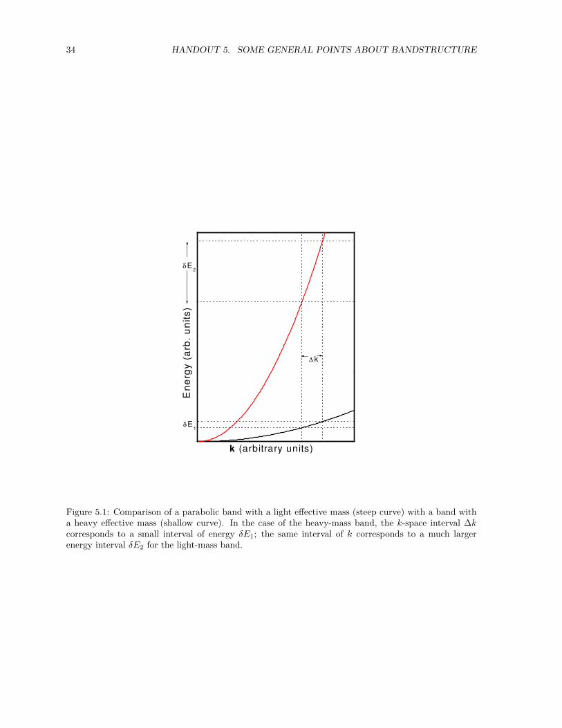
34 HANDOUT 5. SOME GENERAL POINTS ABOUT BANDSTRUCTURE
∆ k
δ E2
δ E1
En
erg
y (a
rb.
un
its)
k (arbitrary units)
Figure 5.1: Comparison of a parabolic band with a light effective mass (steep curve) with a band witha heavy effective mass (shallow curve). In the case of the heavy-mass band, the k-space interval ∆kcorresponds to a small interval of energy δE1; the same interval of k corresponds to a much largerenergy interval δE2 for the light-mass band.
5.3. GENERAL (NON-ISOTOPIC) DENSITY OF STATES 35
1. k is not the (physical momentum/h) of the electron; it is a quantum number describing theelectron’s state within a band. Each band is labelled using the index j.
2. For each j, k takes all values consistent with the Born–von Karman boundary conditions withinthe first Brillouin zone; in our notation k runs though all q. j can run through an infinite numberof discrete values.
3. For a given j, the electronic dispersion relationship Ej(k) has no explicit form; the only constraintis that it must be periodic, i.e. Ej(k) = Ej(k + G).
4. The velocity of an electron with energy Ej(k) is given by v = 1h∇kEj(k).
5. The rate of change of k under the action of an external force f is given by hdkdt = f .
6. The electronic wavefunction is ψ(r) = eik.ruj,k, where uj,k(r) = uj,k(r + T). Here uj,k(r) has nosimple explicit form.
The above list tells us all we need to know about the dynamics of electrons in solids. Let us imagine for aline or two that we know nothing about bands; a calculation of the motion of an electron in a solid due toan external force seems intractable, as the electron is also subject to a complex array of forces from theionic cores/molecules in the crystal. Band theory gets round this problem very effectively. The externalforce results in a time-dependent quantum number k(t). The resulting electronic velocity is obtainedfrom the bandstructure using v = (1/h)∇kEj(k) and substituting k = k(t). The bandstructure thustells us all that we need to know about the interaction between the electrons and the relatively staticcomponents of the crystal (ions, molecules etc.).
5.2.6 Scattering in the Bloch approach
The Bloch wavefunctions describe states which are stationary solutions to the Schrodinger equation ofa periodic potential. Thus these states persist for ever and ever in a perfectly periodic infinite crystal;there will be no scattering of electrons in the absence of disorder (which disturbs the perfect periodicity)or boundaries (which destroy the periodicity/infiniteness of the crystal). This is a manifestation of thewave-like nature of electrons; in a periodic array of scatterers a wave can propogate without attenuationbecause of the coherent constructive interference of the scattered waves. Scattering only takes placebecause of lack of periodicity in r-space.
This observation is in great contrast with the Drude model (where electrons were pictured crashinginto virtually every ion) and the Sommerfeld approach (where scattering was acknowledged but itscause was a mystery). In addition
• it encompasses all possible causes of scattering (phonons, other electrons, impurities and bound-aries, all of which disturb the local periodicity);
• it explains the enormous low-temperature scattering lengths observed in very pure single crystalsof metals (often ∼ mm or even cm);
• it removes the need for the hand-waving explanations as to why the electrons in a metal “mightnot see the ionic cores very much” used to justify the Drude and Sommerfeld approaches.
5.3 General (non-isotopic) density of states
In Section 5.2.4 we considered the density of states g(E) where E(|k|), i.e. in the special case ofisotropic systems. However in non-isotropic materials we may still need to know the density of statesat a particular point in k-space. In this section we will treat the more general case of non-isotropicmaterials, where the density of states at is expressed as g(E(k)).
g(E(k)) =∑ν
gν(Eν(k)) (5.15)
36 HANDOUT 5. SOME GENERAL POINTS ABOUT BANDSTRUCTURE
where
gν(Eν(k)) =
1π
1|∇kE| 1D
12π2
∫l
dl|∇kE| 2D
14π3
∫ ∫S
dS|∇kE| 3D
(5.16)
Discussion of and a method showing how to obtain these results will presented in thelecture
5.3.1 Van Hove singularities
This section will also be presented in lectures on the board
5.4 Holes
It is going to be useful to be able to describe a few empty states close to the top of an almost full bandusing the concept of holes. Consider a band, containing electrons with quantum numbers kj , velocitiesvj and energies E(kj), where E = 0 is at the top of the band. For a full band, the values of k shouldall sum to zero, i.e. ∑
j
kj = 0. (5.17)
We consider removing one electron to create an excitation which we label a hole. Suppose that the lthelectron is removed; the band then acquires a net k which we attribute to the presence of the hole. Thehole has k = kh, with
kh =∑j 6=l
kj = −kl. (5.18)
It is obvious that the lower down the band the empty state, the more excited the system. The hole’senergy Eh must therefore take the form
Eh = −E(kl). (5.19)
The group velocity vh associated with the hole is
vh =1
h∇kh
Eh =1
h∇−kl(−E(kl)) = vl, (5.20)
where the minus signs in Equations 5.18 and 5.19 have cancelled each other.The full band will carry no current, i.e. ∑
j
(−e)vj = 0; (5.21)
the removal of the pth electron produces a current∑j 6=l
(−e)vj = −(−e)vl = (+e)vh, (5.22)
i.e. the hole appears to have an associated positive charge. Finally, substitution of Equations 5.18 and5.19 into Equation 5.12 shows that the effective mass m∗h (or effective mass tensor components in amore complex band) associated with the hole is given by
m∗h = −m∗l . (5.23)
The importance of holes stems from the fact that bands are often well-characterised only close tothe band extrema. Our knowledge of the dispersion relationships away from a particular extremum isoften rather nebulous; such regions are not easily studied experimentally. It is therefore easier to dealwith a small number of empty states close to the well-characterised maximum of an almost full bandrather than attempt to treat the huge number of poorly-characterised states lower down in the band.
5.5. POSTSCRIPT. 37
The fact that holes behave as though they have positive charge and positive effective mass explainswhy many di- and trivalent metals have positive Hall coefficients (see Section 1.3.3 and Table 1.1). Asimple instance in which this could happen is shown in Figure 3.2. The section of Fermi surface in thecorner of the Brillouin zone (Figure 3.2(d)) corresponds to a small number of empty states at the top ofa band; the states are therefore hole-like. By contrast, the sections of Fermi surface straddling the zoneboundaries (Figure 3.2(e)) represent a few filled states at the bottom of the upper band; these statesare therefore electron-like. The observed Hall coefficient would depend on the relative contributionsthat the various Fermi-surface sections make to the electrical conductivity.
5.5 Postscript.
We have now derived all of the ideas needed for a reasonable understanding of the bandstructures of realsolids. We shall take these ideas and use them to study the properties of semiconductors and insulatorsin the following lecture.
5.6 Reading.
A simple treatment is found in e.g. Electricity and Magnetism, by B.I. Bleaney and B. Bleaney,revised third/fourth editions (Oxford University Press, Oxford) Sections 12.4 and 12.5, and a morecomprehensive version is available in Solid State Physics, by N.W Ashcroft and N.D. Mermin (Holt,Rinehart and Winston, New York 1976) Chapter 12.
A higher-level description of the general properties of several different types of bandstructure calcu-lation is given in Semiconductor Physics, by K. Seeger (Springer, Berlin 1991) Chapter 2, Electrons inmetals, by J.M. Ziman (Taylor and Francis) and (harder) Fundamentals of semiconductors, by P. Yuand M. Cardona (Springer, Berlin, 1996) Chapter 2.

38 HANDOUT 5. SOME GENERAL POINTS ABOUT BANDSTRUCTURE
Handout 6
Semiconductors and Insulators
The most important aspect of semiconductor1 bandstructure may be summarised as follows; at absolutezero the highest completely filled band (the valence band) is separated from the lowest empty band (theconduction band) by an energy gap or band gap Eg of forbidden states. Therefore the material doesnot conduct electricity at T = 0. At finite temperatures a variety of processes enable electrons to beexcited into the conduction band and empty states to occur in the valence band, thus allowing electricalconduction. However, we shall see that the presence of the energy gap still dominates the properties ofthe semiconductor.
Most of the technologically-important semiconductors, such as Ge, Si, GaAs and (Hg,Cd)Te, have aface-centred-cubic lattice with a two-atom basis; this is illustrated in Figure 6.1. In the case of Si andGe, the atoms on the A and B sites in Figure 6.1 are identical (the so-called diamond structure). Inthe case of binary semiconductors such as (for example) GaAs the A sites will have Ga atoms and theB sites As atoms; the crystal is said to have the zinc blende structure. As stated above, in each case,the underlying lattice is face-centred cubic and there is a two atom basis. Thus, both the group IVelements and many of the binary semiconductors such as GaAs have the same shape of first Brillouinzone, which is shown in Figure 6.1 and which will be useful for understanding the band diagrams in thefollowing discussion.
6.1 Bandstructure of Si and Ge
6.1.1 General points
Si and Ge were the first semiconductors to be exploited commercially, and Si continues to be veryimportant as a technological material. 2 Figures 6.2 and 6.3 show calculations of the bandstructuresof Si and Ge respectively. At first sight, the situation looks a complex, fearful mess. However, atthe typical temperatures that will concern us (0− ∼ 300 K), the only dramatic action (i.e. thermalexcitation of electrons and holes, optical absorption edges) will occur close to the highest point in thevalence band and the lowest points in the conduction band.
6.1.2 Heavy and light holes
In both Si and Ge, two bands converge at the valence band maximum in the Brillouin-zone centre (theΓ-point). These bands are known as the heavy- and light-hole bands; the flatter one, with its large valueof (d2E/dk2)−1, is the heavy hole band, and the steeper one the light hole band (for obvious reasons–see Figure 5.1).
The heavy holes tend to dominate the properties of the valence-band extremum; their heaviereffective mass means that their density of states will be much larger than that of the light holes (seeSection 5.2.4).
1For brevity I shall refer to such materials collectively as “semiconductors”; as we shall see, the distinction between asemiconductor and an insulator is fairly nebulous.
2See e.g. Semiconductor Physics, by K. Seeger (Springer, Berlin 1991) Section 5.7 and references therein.
39
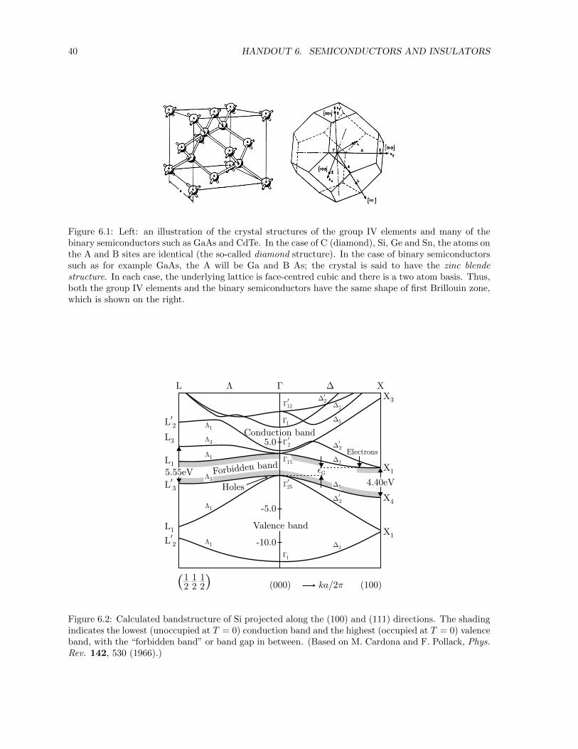
40 HANDOUT 6. SEMICONDUCTORS AND INSULATORS
Figure 6.1: Left: an illustration of the crystal structures of the group IV elements and many of thebinary semiconductors such as GaAs and CdTe. In the case of C (diamond), Si, Ge and Sn, the atoms onthe A and B sites are identical (the so-called diamond structure). In the case of binary semiconductorssuch as for example GaAs, the A will be Ga and B As; the crystal is said to have the zinc blendestructure. In each case, the underlying lattice is face-centred cubic and there is a two atom basis. Thus,both the group IV elements and the binary semiconductors have the same shape of first Brillouin zone,which is shown on the right.
L0
2
¢1
¢1
¢5
¢0
2
¢0
2
¢0
2
L3
L1
L1
L0
3
L0
2
L ¤
¤1
¤1
¤1
¤1
¤3
¢X3
X1
4.40eV5.55eV
X¡
¡0
25
¡0
12
¡1
¡1
¡0
2
Holes
Electrons
X1
X4
¢1
¢5
²GFo denrbid band
Conduction band
Valence band
¤3
¡15
-5.0
-10.0
5.0
12
12
12( ) (000) (100)ka/2¼
Figure 6.2: Calculated bandstructure of Si projected along the (100) and (111) directions. The shadingindicates the lowest (unoccupied at T = 0) conduction band and the highest (occupied at T = 0) valenceband, with the “forbidden band” or band gap in between. (Based on M. Cardona and F. Pollack, Phys.Rev. 142, 530 (1966).)
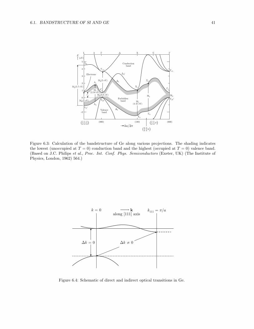
6.1. BANDSTRUCTURE OF SI AND GE 41
¢ 02
¡0
2
L 03
L3
L ¤
¤1
¤3
¢
X4
X¡ ¡§
¡250¡ 0
25
Electrons
X1
¢5
¢1
²G
Forbiddenband
Conductionband
Valenceband
¡1.5
¡2
¡15
-2
12
12
12( ) 1
212( )
34
34( )
(000)(000) (100)
ka/2¼
§4
§1
(eV)
5
4
3
2
1
0
M (5.7 eV)3
M2M0
M(4.45 eV)
1
M(2.18 eV)
1
M (3 eV)0
M (0.8 eV)0
M (2 eV)0
0
0
E
Figure 6.3: Calculation of the bandstructure of Ge along various projections. The shading indicatesthe lowest (unoccupied at T = 0) conduction band and the highest (occupied at T = 0) valence band.(Based on J.C. Philips et al., Proc. Int. Conf. Phys. Semiconductors (Exeter, UK) (The Institute ofPhysics, London, 1962) 564.)
k ¼111 = /a
¢ = 0k
k = 0along [111] axis
k
¢ = 0k
Figure 6.4: Schematic of direct and indirect optical transitions in Ge.

42 HANDOUT 6. SEMICONDUCTORS AND INSULATORS
6.1.3 Optical absorption
Photons with energy hν ∼ Eg ∼ 0− 2 eV will have wavevectors which are typical Brillouin-zone size(energetic X-rays (hν 1 eV) have wavevectors ∼ Brillouin-zone size). This means that transitionsinvolving the absorption of a photon to excite an electron from the valence band to the conductionband, leaving a hole behind, will be essentially vertical in k-space. The transition strengths will begreatest when the joint density of initial and final states is large, i.e. when conduction and valencebands are approximately parallel.
Note that Si and Ge are indirect-gap semiconductors; the smallest band separation (the thermody-namic band gap, which determines the thermal population of electron and hole states) is not vertical ink-space. Figure 6.4 shows a schematic representation of this situation in Ge; strong optical transitionswill occur at the point labelled ∆k = 0 on the diagram, at a higher energy than the thermodynamicband gap, which is labelled ∆k 6= 0.
It turns out that optical transitions can occur at energies close to the thermodynamic band gap inSi and Ge if both a phonon and a photon are involved; emission or (at higher temperatures) absorptionof a phonon with the appropriate wavevector allows momentum to be conserved so that the transitionslabelled ∆k 6= 0 in Figure 6.4 are possible.
Figure 6.5 shows the optical absorption coefficient of Ge at 300 K and 77 K. Both the indirect(∆k 6= 0) and direct (∆k = 0) transitions can be seen as absorption edges. The higher energy directtransition is some 100 times stronger than the indirect transition. In addition, the indirect transition isstronger at 300 K than at 77 K, as there is a substantial population of phonons of a suitable wavevector totake part in the transition at the higher temperature; optical transitions assisted by phonon absorptionthus becomes possible in addition to those assisted by emission.
Finally, note that the energy gaps change with temperature. This is not unexpected in models ofbandstructure; e.g. in the tight-binding model of bands, thermal expansion will influence the atomicseparation and hence the transfer integrals.
6.1.4 Constant energy surfaces in the conduction bands of Si and Ge
The conduction band minima in Si and Ge (see Figure 6.2 and 6.3) are situated away from the Brillouin-zone centre (the Γ point) and are thus rather anisotropic. At energies close to (i.e. <∼ 50− 100 meVfrom) the bottom of the conduction bands, effective mass tensors with constant coefficients (as discussedin the problems) can be used to describe the conduction-band minima in Si and Ge. By choosing suitableaxes, the tensors can be made diagonal. The constant energy surfaces are approximate ellipsoids ofrotation about one of these axes (see Figure 6.6).
6.2 Bandstructure of the direct-gap III-V and II-VI semicon-ductors
6.2.1 Introduction
Compound semiconductors such as GaAs and InSb are known as III-V semiconductors because theycombine elements from groups III and V of the Periodic Table. In a similar way, semiconductorssuch as (Cd,Hg)Te are known as II-VI semiconductors. Many III-V and II-VI semiconductors havetechnological applications, often as emitters and detectors of electromagnetic radiation. It is importantthat we examine their bandstructure and consequent properties, in order to see why they are used forsuch applications. We shall see that one of the most important points is that the minimum energyband-gaps in these materials are direct, so that optical transitions with ∆k ≈ 0 can occur.
6.2.2 General points
Figure 6.7 shows the Brillouin zone and calculated bandstructure of GaAs, a typical direct-gap III-Vsemiconductor. Note that
• both heavy- and light-hole bands are present at the valence-band extremum, as before (c.f. Fig-ure 6.3);
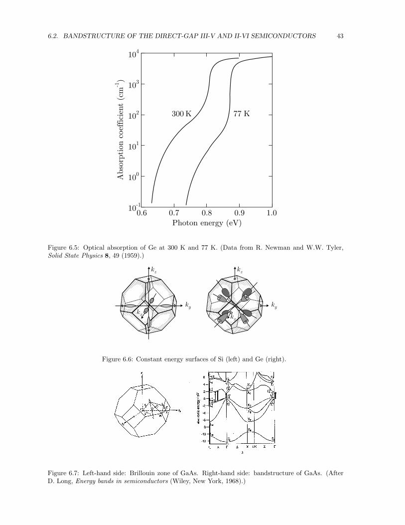
6.2. BANDSTRUCTURE OF THE DIRECT-GAP III-V AND II-VI SEMICONDUCTORS 43
104
103
102
101
100
10-1
300 K 77 K
0.6 0.7 0.8 0.9 1.0Photon energy (eV)
Abso
rpti
on c
oef
fici
ent
(cm
)-1
Figure 6.5: Optical absorption of Ge at 300 K and 77 K. (Data from R. Newman and W.W. Tyler,Solid State Physics 8, 49 (1959).)
kz
ky
kx
kz
ky
kx
Figure 6.6: Constant energy surfaces of Si (left) and Ge (right).
Figure 6.7: Left-hand side: Brillouin zone of GaAs. Right-hand side: bandstructure of GaAs. (AfterD. Long, Energy bands in semiconductors (Wiley, New York, 1968).)
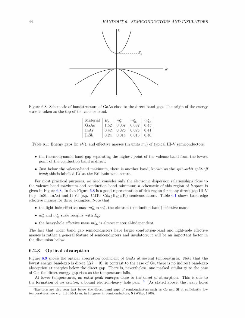
44 HANDOUT 6. SEMICONDUCTORS AND INSULATORS
k
E
Eg
Figure 6.8: Schematic of bandstructure of GaAs close to the direct band gap. The origin of the energyscale is taken as the top of the valence band.
Material Eg m∗c m∗lh m∗hh
GaAs 1.52 0.067 0.082 0.45InAs 0.42 0.023 0.025 0.41InSb 0.24 0.014 0.016 0.40
Table 6.1: Energy gaps (in eV), and effective masses (in units me) of typical III-V semiconductors.
• the thermodynamic band gap separating the highest point of the valence band from the lowestpoint of the conduction band is direct;
• Just below the valence-band maximum, there is another band, known as the spin-orbit split-offband; this is labelled ΓV
7 at the Brillouin-zone centre.
For most practical purposes, we need consider only the electronic dispersion relationships close tothe valence band maximum and conduction band minimum; a schematic of this region of k-space isgiven in Figure 6.8. In fact Figure 6.8 is a good representation of this region for many direct-gap III-V(e.g. InSb, InAs) and II-VI (e.g. CdTe, Cd0.2Hg0.8Te) semiconductors. Table 6.1 shows band-edgeeffective masses for three examples. Note that
• the light-hole effective mass m∗lh ≈ m∗c , the electron (conduction-band) effective mass;
• m∗c and m∗lh scale roughly with Eg;
• the heavy-hole effective mass m∗hh is almost material-independent.
The fact that wider band gap semiconductors have larger conduction-band and light-hole effectivemasses is rather a general feature of semiconductors and insulators; it will be an important factor inthe discussion below.
6.2.3 Optical absorption
Figure 6.9 shows the optical absorption coefficient of GaAs at several temperatures. Note that thelowest energy band-gap is direct (∆k = 0); in contrast to the case of Ge, there is no indirect band-gapabsorption at energies below the direct gap. There is, nevertheless, one marked similarity to the caseof Ge; the direct energy-gap rises as the temperature falls.
At lower temperatures, an extra peak emerges close to the onset of absorption. This is due tothe formation of an exciton, a bound electron-heavy hole pair. 3 (As stated above, the heavy holes
3Excitons are also seen just below the direct band gaps of semiconductors such as Ge and Si at sufficiently lowtemperatures; see e.g. T.P. McLean, in Progress in Semiconductors, 5 (Wiley, 1960).
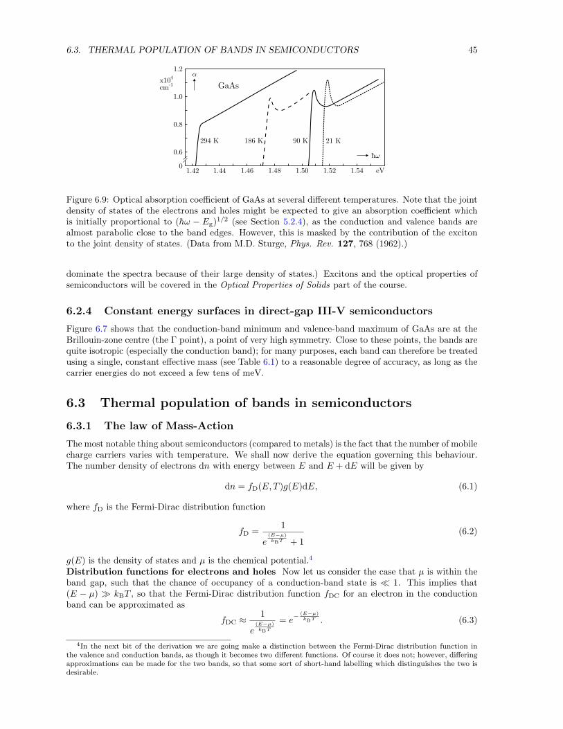
6.3. THERMAL POPULATION OF BANDS IN SEMICONDUCTORS 45
0.6
0.8
1.0
1.2
01.42 1.44 1.46 1.48 1.50 1.52 1.54 eV
294 K 186 K 90 K 21 K
h!
GaAs
®
x10
cm
4
-1
Figure 6.9: Optical absorption coefficient of GaAs at several different temperatures. Note that the jointdensity of states of the electrons and holes might be expected to give an absorption coefficient whichis initially proportional to (hω − Eg)1/2 (see Section 5.2.4), as the conduction and valence bands arealmost parabolic close to the band edges. However, this is masked by the contribution of the excitonto the joint density of states. (Data from M.D. Sturge, Phys. Rev. 127, 768 (1962).)
dominate the spectra because of their large density of states.) Excitons and the optical properties ofsemiconductors will be covered in the Optical Properties of Solids part of the course.
6.2.4 Constant energy surfaces in direct-gap III-V semiconductors
Figure 6.7 shows that the conduction-band minimum and valence-band maximum of GaAs are at theBrillouin-zone centre (the Γ point), a point of very high symmetry. Close to these points, the bands arequite isotropic (especially the conduction band); for many purposes, each band can therefore be treatedusing a single, constant effective mass (see Table 6.1) to a reasonable degree of accuracy, as long as thecarrier energies do not exceed a few tens of meV.
6.3 Thermal population of bands in semiconductors
6.3.1 The law of Mass-Action
The most notable thing about semiconductors (compared to metals) is the fact that the number of mobilecharge carriers varies with temperature. We shall now derive the equation governing this behaviour.The number density of electrons dn with energy between E and E + dE will be given by
dn = fD(E, T )g(E)dE, (6.1)
where fD is the Fermi-Dirac distribution function
fD =1
e(E−µ)kBT + 1
(6.2)
g(E) is the density of states and µ is the chemical potential.4
Distribution functions for electrons and holes Now let us consider the case that µ is within theband gap, such that the chance of occupancy of a conduction-band state is 1. This implies that(E − µ) kBT , so that the Fermi-Dirac distribution function fDC for an electron in the conductionband can be approximated as
fDC ≈1
e(E−µ)kBT
= e− (E−µ)
kBT . (6.3)
4In the next bit of the derivation we are going make a distinction between the Fermi-Dirac distribution function inthe valence and conduction bands, as though it becomes two different functions. Of course it does not; however, differingapproximations can be made for the two bands, so that some sort of short-hand labelling which distinguishes the two isdesirable.
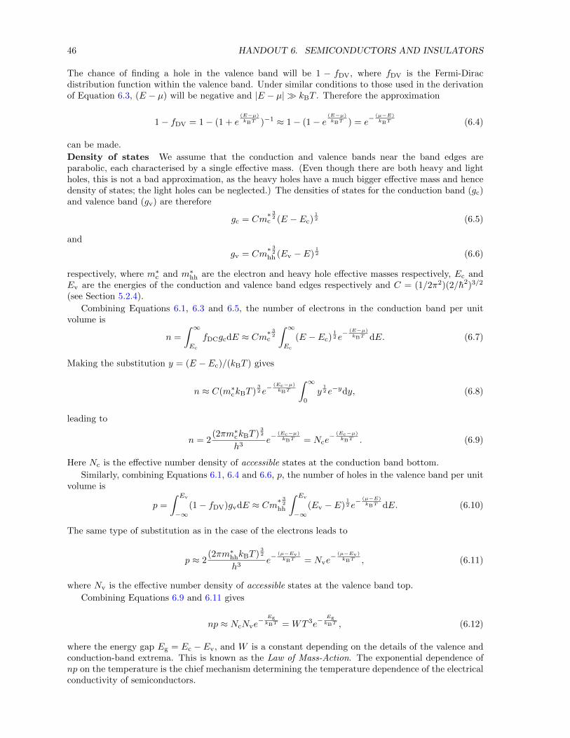
46 HANDOUT 6. SEMICONDUCTORS AND INSULATORS
The chance of finding a hole in the valence band will be 1 − fDV, where fDV is the Fermi-Diracdistribution function within the valence band. Under similar conditions to those used in the derivationof Equation 6.3, (E − µ) will be negative and |E − µ| kBT . Therefore the approximation
1− fDV = 1− (1 + e(E−µ)kBT )−1 ≈ 1− (1− e
(E−µ)kBT ) = e
− (µ−E)kBT (6.4)
can be made.
Density of states We assume that the conduction and valence bands near the band edges areparabolic, each characterised by a single effective mass. (Even though there are both heavy and lightholes, this is not a bad approximation, as the heavy holes have a much bigger effective mass and hencedensity of states; the light holes can be neglected.) The densities of states for the conduction band (gc)and valence band (gv) are therefore
gc = Cm∗ 3
2c (E − Ec)
12 (6.5)
and
gv = Cm∗ 3
2
hh (Ev − E)12 (6.6)
respectively, where m∗c and m∗hh are the electron and heavy hole effective masses respectively, Ec andEv are the energies of the conduction and valence band edges respectively and C = (1/2π2)(2/h2)3/2
(see Section 5.2.4).
Combining Equations 6.1, 6.3 and 6.5, the number of electrons in the conduction band per unitvolume is
n =
∫ ∞Ec
fDCgcdE ≈ Cm∗32
c
∫ ∞Ec
(E − Ec)12 e− (E−µ)
kBT dE. (6.7)
Making the substitution y = (E − Ec)/(kBT ) gives
n ≈ C(m∗ckBT )32 e− (Ec−µ)
kBT
∫ ∞0
y12 e−ydy, (6.8)
leading to
n = 2(2πm∗ckBT )
32
h3e− (Ec−µ)
kBT = Nce− (Ec−µ)
kBT . (6.9)
Here Nc is the effective number density of accessible states at the conduction band bottom.
Similarly, combining Equations 6.1, 6.4 and 6.6, p, the number of holes in the valence band per unitvolume is
p =
∫ Ev
−∞(1− fDV)gvdE ≈ Cm∗
32
hh
∫ Ev
−∞(Ev − E)
12 e− (µ−E)
kBT dE. (6.10)
The same type of substitution as in the case of the electrons leads to
p ≈ 2(2πm∗hhkBT )
32
h3e− (µ−Ev)
kBT = Nve− (µ−Ev)
kBT , (6.11)
where Nv is the effective number density of accessible states at the valence band top.
Combining Equations 6.9 and 6.11 gives
np ≈ NcNve− EgkBT = WT 3e
− EgkBT , (6.12)
where the energy gap Eg = Ec − Ev, and W is a constant depending on the details of the valence andconduction-band extrema. This is known as the Law of Mass-Action. The exponential dependence ofnp on the temperature is the chief mechanism determining the temperature dependence of the electricalconductivity of semiconductors.
6.3. THERMAL POPULATION OF BANDS IN SEMICONDUCTORS 47
273
300
400
500
600
800
1400
1018 1016 1014 1012 1010 108
Intrinsic carrier concentration, i (cm )n-3
4
3
2
1
1000/
( K)
T-1
T(K
)
GaAsGe Si
Figure 6.10: Calculated intrinsic carrier densities ni versus temperature in Ge (Eg = 0.74 eV), Si(Eg = 1.17 eV) and GaAs (Eg = 1.52 eV).
6.3.2 The motion of the chemical potential
We now consider what happens to the chemical potential as a function of T . Setting n = p and equatingEquations 6.9 and 6.11 gives
Nc
Nv= e
(2µ−Ec−Ev)kBT . (6.13)
Now (Nc/Nv) = (m∗c/m∗hh)3/2 (see Section 5.2.4), so that the chemical potential is given by
µ =1
2(Ec + Ev) +
3
4kBT ln
(m∗hh
m∗c
). (6.14)
Therefore µ starts off in the middle of the bandgap (i.e. exactly half way between the empty and fullstates) at T = 0; as m∗hh is bigger than m∗c in most semiconductors, µ usually moves up as T rises.
6.3.3 Intrinsic carrier density
Let us first assume that the only source of electrons in the conduction band and holes in the valence bandis the thermal excitation of electrons across the band gap (i.e. there are no impurities; see Section 6.3.4below); such electrons and holes are known as intrinsic carriers. In this case (see Equation 6.12)
ni = n = p = T32W
12 e− Eg
2kBT , (6.15)
where ni is the intrinsic carrier density. Note that the exponential contains Eg/2 and not Eg; this isbecause the creation of each electron in the conduction band automatically makes a hole in the valenceband.
Figure 6.10 shows ni for Ge, Si and GaAs as a function of T ; the exponential dependence on Eg
means that relatively small differences in band gap result in nis which are several orders of magnitudeapart.
6.3.4 Impurities and extrinsic carriers
For virtually all practical applications (i.e. those at room temperature), the conductivity of semicon-ductors such as GaAs, Ge and Si is dominated by extrinsic carriers, those provided by doping thesemiconductor with impurities.
Two types of impurity will concern us, donors, which donate electrons, and acceptors, which provideholes.
• Donors An atom of the semiconductor with valence V is replaced by a donor atom, with valenceV + 1. After the donor has bonded into the host lattice, it will still have one electron left over.Examples of donors include P in Si or Ge, Si on a Ga site in GaAs, and Te on an As site in GaAs.
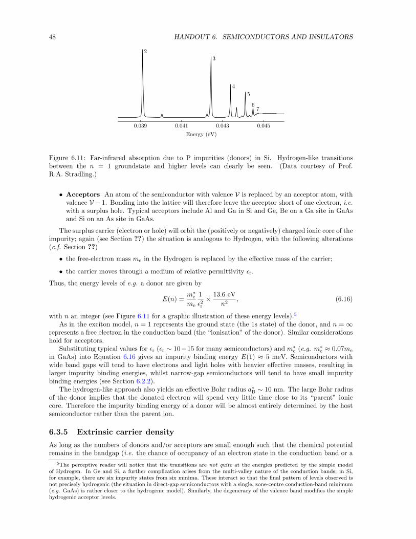
48 HANDOUT 6. SEMICONDUCTORS AND INSULATORS
2
3
4
5
67
0.039 0.041 0.043 0.045
Energy (eV)
Figure 6.11: Far-infrared absorption due to P impurities (donors) in Si. Hydrogen-like transitionsbetween the n = 1 groundstate and higher levels can clearly be seen. (Data courtesy of Prof.R.A. Stradling.)
• Acceptors An atom of the semiconductor with valence V is replaced by an acceptor atom, withvalence V − 1. Bonding into the lattice will therefore leave the acceptor short of one electron, i.e.with a surplus hole. Typical acceptors include Al and Ga in Si and Ge, Be on a Ga site in GaAsand Si on an As site in GaAs.
The surplus carrier (electron or hole) will orbit the (positively or negatively) charged ionic core of theimpurity; again (see Section ??) the situation is analogous to Hydrogen, with the following alterations(c.f. Section ??)
• the free-electron mass me in the Hydrogen is replaced by the effective mass of the carrier;
• the carrier moves through a medium of relative permittivity εr.
Thus, the energy levels of e.g. a donor are given by
E(n) =m∗cme
1
ε2r× 13.6 eV
n2, (6.16)
with n an integer (see Figure 6.11 for a graphic illustration of these energy levels).5
As in the exciton model, n = 1 represents the ground state (the 1s state) of the donor, and n =∞represents a free electron in the conduction band (the “ionisation” of the donor). Similar considerationshold for acceptors.
Substituting typical values for εr (εr ∼ 10−15 for many semiconductors) and m∗c (e.g. m∗c ≈ 0.07me
in GaAs) into Equation 6.16 gives an impurity binding energy E(1) ≈ 5 meV. Semiconductors withwide band gaps will tend to have electrons and light holes with heavier effective masses, resulting inlarger impurity binding energies, whilst narrow-gap semiconductors will tend to have small impuritybinding energies (see Section 6.2.2).
The hydrogen-like approach also yields an effective Bohr radius a∗B ∼ 10 nm. The large Bohr radiusof the donor implies that the donated electron will spend very little time close to its “parent” ioniccore. Therefore the impurity binding energy of a donor will be almost entirely determined by the hostsemiconductor rather than the parent ion.
6.3.5 Extrinsic carrier density
As long as the numbers of donors and/or acceptors are small enough such that the chemical potentialremains in the bandgap (i.e. the chance of occupancy of an electron state in the conduction band or a
5The perceptive reader will notice that the transitions are not quite at the energies predicted by the simple modelof Hydrogen. In Ge and Si, a further complication arises from the multi-valley nature of the conduction bands; in Si,for example, there are six impurity states from six minima. These interact so that the final pattern of levels observed isnot precisely hydrogenic (the situation in direct-gap semiconductors with a single, zone-centre conduction-band minimum(e.g. GaAs) is rather closer to the hydrogenic model). Similarly, the degeneracy of the valence band modifies the simplehydrogenic acceptor levels.
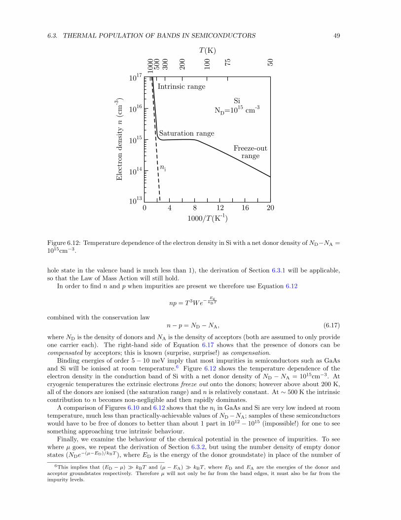
6.3. THERMAL POPULATION OF BANDS IN SEMICONDUCTORS 49
100
0500
300
200
100 75
50
Intrinsic range
Saturation range
Freeze-outrange
Si
N =10 cmD15 -3
T(K)
ni
0 4 8 12 16 20
1017
1016
1015
1014
1013
1000/ (K )T-1
Ele
ctro
n d
ensi
ty(c
m)
n-3
Figure 6.12: Temperature dependence of the electron density in Si with a net donor density ofND−NA =1015cm−3.
hole state in the valence band is much less than 1), the derivation of Section 6.3.1 will be applicable,so that the Law of Mass Action will still hold.
In order to find n and p when impurities are present we therefore use Equation 6.12
np = T 3We− EgkBT
combined with the conservation lawn− p = ND −NA, (6.17)
where ND is the density of donors and NA is the density of acceptors (both are assumed to only provideone carrier each). The right-hand side of Equation 6.17 shows that the presence of donors can becompensated by acceptors; this is known (surprise, surprise!) as compensation.
Binding energies of order 5 − 10 meV imply that most impurities in semiconductors such as GaAsand Si will be ionised at room temperature.6 Figure 6.12 shows the temperature dependence of theelectron density in the conduction band of Si with a net donor density of ND − NA = 1015cm−3. Atcryogenic temperatures the extrinsic electrons freeze out onto the donors; however above about 200 K,all of the donors are ionised (the saturation range) and n is relatively constant. At ∼ 500 K the intrinsiccontribution to n becomes non-negligible and then rapidly dominates.
A comparison of Figures 6.10 and 6.12 shows that the ni in GaAs and Si are very low indeed at roomtemperature, much less than practically-achievable values of ND−NA; samples of these semiconductorswould have to be free of donors to better than about 1 part in 1012 − 1015 (impossible!) for one to seesomething approaching true intrinsic behaviour.
Finally, we examine the behaviour of the chemical potential in the presence of impurities. To seewhere µ goes, we repeat the derivation of Section 6.3.2, but using the number density of empty donorstates (NDe
−(µ−ED)/kBT ), where ED is the energy of the donor groundstate) in place of the number of
6This implies that (ED − µ) kBT and (µ − EA) kBT , where ED and EA are the energies of the donor andacceptor groundstates respectively. Therefore µ will not only be far from the band edges, it must also be far from theimpurity levels.

50 HANDOUT 6. SEMICONDUCTORS AND INSULATORS
holes in the valence band.7 (We are thus considering an n-type semiconductor; however, an equivalentderivation for a p-type semiconductor uses the same ideas.) This gives
µ =1
2(ED + Ec) +
1
2kBT ln(
ND
Nc), (6.18)
i.e. µ can either rise or fall with increasing temperature.8
6.3.6 Degenerate semiconductors.
Once all of the donors are ionised (the exhaustion regime), n = ND; equating Equation 6.9 to ND gives
µ ≈ Ec + kBT ln(ND
Nc), (6.19)
where the ≈ re-emphasises that we are approaching a dodgy situtation as far as the approximationsused to derive Equation 6.3 are concerned. There are two cases to note.
• ND < Nc leads to a chemical potential which is still in the bandgap. The number of electrons inthe conduction band is still small compared to the number of available states, so that the quasi–classical statistics used in Equation 6.3 and the derivation that follows it are probably valid. Inthis case, the semiconductor is non-degenerate.
• ND > Nc leads to a chemical potential in the conduction band. Therefore we cannot use the quasi-classical approximation for the Fermi-Dirac distribution function. The semiconductor behavessomewhat like a metal and is said to be degenerate.
6.3.7 Impurity bands
If a large enough concentration of impurities is placed in a semiconductor, the wavefunctions of thecarriers bound to the impurities will start to overlap; the criterion for this for e.g donors is ND ≥∼ 1/a∗3B .The situation becomes rather similar to the tight-binding model, and carriers will be able to movefrom impurity to impurity. The semiconductor will remain electrically conductive even at very lowtemperatures; it is another instance of a degenerate semiconductor. However, in contrast to the casediscussed in the previous section, the chemical potential will depend rather less on the temperature; wewill have a situation much more analogous to a (rather dirty) conventional metal.
6.3.8 Is it a semiconductor or an insulator?
Most textbooks state that insulators are just wide-gap semiconductors, the implication being thatthermal effects excite a negligible number of electron-hole pairs across the band gap if it is wide (seeEquation 6.12).
However, this picture is an over-simplification; as we have seen, the carriers which populate thebands at room temperature come mostly from impurities. Section 6.2.2 stated that carrier effectivemasses become heavier as the band gap increases; as the effective mass increases, the impurity bindingenergy will increase (see Equation 6.16). As the gap widens, eventually the impurity will become sodeep that it will not be ionised at room temperature.
The distinction between wide-gap semiconductors and insulators is very blurred; e.g. studies ofdoped diamond for use in potential ultra-violet/blue LEDs are carried out, the aim being to finddonors and acceptors which are shallow enough not to lead to carrier freeze-out at sensible operating
7So as not to complicate the discussion, the expression used for the number of empty donor states is a simplification.Those intending to embark on research should note that the number should be ND(1− 1/(1 + g−1e(µ−ED)/kBT )), whereg is the degeneracy of the donor groundstate. To see where g comes from, consider the 1s state of a hydrogenic donor.This is technically doubly degenerate owing to the fact that electrons can have spin up or spin down. Double occupancyof the donor is not energetically favourable; however, the statistical mechanics “knows” that there are two states availableat that energy. See e.g. Semiconductor Physics, by K. Seeger (Springer, Berlin 1991).
8Beware! The derivation of this Equation assumes that Ec−µ and µ−ED are both much greater than kBT . We havealready seen that Ec−ED >∼ kBT at room temperature; therefore this formula is only valid at much lower temperatures.It is, nevertheless, a useful guide to the low-temperature movement of µ.
6.4. READING. 51
temperatures of ∼ 300 K. Conversely, much work has been done to dope semiconductors like GaAswith so-called deep traps, impurity states which are deliberately made so deep that the electrons andholes will remain frozen on them even at room temperature. Excess impurities will “soak up” any othercarriers that are around, giving very high resistivities indeed. Such semi-insulating material is oftenused as a substrate to support devices made from more highly-conductive GaAs and (Ga,Al)As.
6.3.9 A note on photoconductivity.
It has been mentioned that semiconductors are often employed to detect photons. The detection involvesphotoconductivity, which can occur via three mechanisms;
1. the creation of electron-hole pairs through interband (intrinsic) absorption of radiation; typicallythis occurs at photon energies ∼ Eg ∼ 1 eV or wavelengths λ ∼ 1 µm; later we shall see that byalloying semiconductors such as CdTe with semimetals such as HgTe, materials with band gapsas small as 0.1 eV (corresponding to λ ∼ 10 µm) can be made;
2. the excitation of electrons (or holes) from donor (acceptor) impurities into the conduction (valence)band; typically this occurs at energies ∼ 5 meV to 50 meV, corresponding to λ ∼ 200− 20 µm;
3. free-carrier absorption.
In cases 1 and 2, the carrier numbers are increased; in case 3, the number of carriers remains constant butthe conductivity changes because of a change in mobility. The latter mechanism is usually important incases where the carrier effective mass is low and the band is strongly nonparabolic 9 as the low densityof band states (from the small effective mass) results in long relaxation times for the excited carriers.Free-carrier absorption is proportional to the real part of the conductivity σ = σ0/(1 + iωτ), and soincreases rapidly at low energies/long wavelengths.
6.4 Reading.
Useful alternative treatments are given in Electricity and Magnetism, by B.I. Bleaney and B. Bleaney,revised third/fourth editions (Oxford University Press, Oxford) Chapters 17-19, Solid State Physics, byG. Burns (Academic Press, Boston, 1995) Sections 10.10-10.20 and Chapter 18, and Low-DimensionalSemiconductor Structures, by M.J. Kelly, (Clarendon Press, Oxford 1995) Chapter 1 and Sections 2.1-2.3, 2.7, 4.4, 5.1-5.3, 9.1-9.2. Optical properties of semiconductors are tackled in depth in OpticalProperties of Solids, by A.M. Fox (OUP 2000).
Essentials of semiconductor physics by Tom Wenckebach (Wiley, New York, 1999) provides a slightlyoffbeat, but algebraically rigorous treatment of many of the properties of semiconductors which wouldbe useful for those embarking on research or calculations. A similarly detailed but more traditionalapproach is given in Semiconductor Physics, by K. Seeger (Springer, Berlin 1991)and Fundamentals ofsemiconductors, by P. Yu and M. Cardona (Springer, Berlin, 1996). The methods used to calculatethe bandstructure of semiconductors have been reviewed by F. Bassani (Chapter 2 of Semiconductorsand Semimetals, Volume 1, edited by R.K. Willardson and A.C. Beer (Academic Press, New York,1966)) and E.O. Kane (Chapter 4 of Handbook on Semiconductors, volume 1, edited by T.S. Moss(North Holand, Amsterdam, 1982)); the latter reference includes the famous k.p method for evaluatingthe bandstructure close to band extrema (see also Fundamentals of semiconductors, by P. Yu and M.Cardona (Springer, Berlin, 1996) Chapter 2.).
A very wide range of properties of semiconductors (band gaps, effective masses etc.) can be looked upin the comprehensive Landholt-Bornstein series, Numerical data and functional relationships in scienceand technology, New Series, Group III, Volume 17, edited by O. Madelung (Springer, Berlin, 1982).
Impurities in semiconductors are dealt with comprehensively in the mammoth tome Doping in III-Vsemiconductors, by E.F. Schubert (Cambridge University Press, 1993).
9This is the case in the conduction bands of narrow-gap semiconductors such as Cd0.2Hg0.8Te and InSb.

52 HANDOUT 6. SEMICONDUCTORS AND INSULATORS
Handout 7
Bandstructure engineering
7.1 Introduction
We shall explore some of the ways in which bands with desired properties can be engineered using whathas been termed “chemical architecture”. A very simple example of this is the use of semiconductoralloys, in which a wide-gap semiconductor and a narrow-gap semiconductor are combined to give asubstance with a desired intermediate bandgap. A second example is the semiconductor superlattice orheterostructure; here, very thin layers of different semiconductors are superimposed.
7.2 Semiconductor alloys
The previous lectures mentioned the fact that direct-gap semiconductors are used in opto-electronicapplications. Many of these applications involve the emission of light by recombination of an electronand a hole across the band gap, or absorption of light of the band-gap energy to create an electron-holepair and hence produce some form of photoconduction;1 The size of the band gap is therefore of greatimportance.
Figure 8.1 shows the band gaps and lattice parameters for some of the more common elemental andbinary semiconductors. The band gaps available are not generally optimised for practical devices. Adesire to improve on this has led to the field of bandstructure engineering, where a variety of artificialstructures are used to provide bandstructure optimised to a particular application.
The simplest bandstructure engineering involves making ternary alloys such as (Ga,Al)As and(Hg,Cd)Te in order to achieve a desired band gap. I list three examples of the uses of such alloys.
Ga1−xAlxAs is technologically important because GaAs and AlAs form a solid solution over theentire (0 ≤ x ≤ 1) composition range with very little variation of lattice parameter (see Figure 8.1);this means that multilayers of very high quality can be fabricated (see below). A variable direct bandgap is obtained for the range 0 ≤ x ≤∼ 0.35; for x ≥∼ 0.35 the band-gap is indirect.
The band gap of Ga1−xInxAs may be adjusted over an energy range which coincides with thelow-attenuation region of many optical fibres.
Hg1−xCdxTe continues to be of great importance in the fabrication of infrared detectors coveringthe 10 µm (x = 0.2; Eg ≈ 100 meV) and 5 µm (x = 0.3; Eg ≈ 200 meV) atmospheric windows (regionswhere the atmosphere has little absorption). The 10 µm region also contains the peak thermal emissionof ∼ 300 K things, including human beings, so that there are a variety of medical (thermal imaging),meteorological and more sinister applications. Exhausts and jet engines emit well in the 5 µm range,and so the applications of Hg1−xCdxTe with x = 0.3 can be easily imagined.
1See e.g. Semiconductor Physics, by K. Seeger (Springer, Berlin 1991) Chapters 12 and 13; Optical Properties ofSolids by Mark Fox, (Oxford University Press, Oxford 2001), Low-Dimensional Semiconductor Structures, by M.J. Kelly,(Clarendon Press, Oxford 1995) Chapter 18.
53
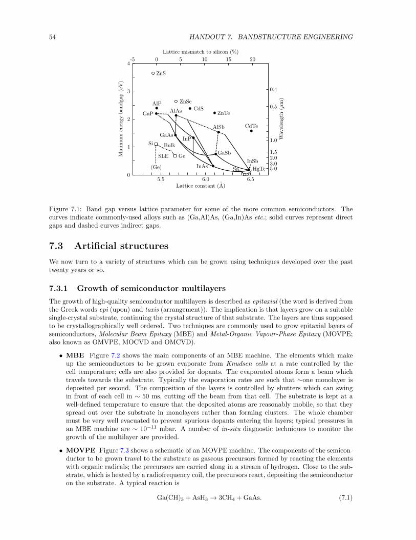
54 HANDOUT 7. BANDSTRUCTURE ENGINEERING
5.5 6.0 6.5Lattice constant (Aº)
-5 0 5 10 15 20
0.4
0.5
1.0
1.52.03.05.0
ZnS
AlP ZnSe
AlAs CdSZnTe
AlSb CdTe
GaP
GaAs
GaSb
Si Bulk
SLE Ge
(Ge) InAsInSb
Sn HgTe
InP
4
3
2
1
0
Wav
elen
gth (
m)
¹
Min
imum
ener
gy b
andga
p (
eV)
Lattice mismatch to silicon (%)
Figure 7.1: Band gap versus lattice parameter for some of the more common semiconductors. Thecurves indicate commonly-used alloys such as (Ga,Al)As, (Ga,In)As etc.; solid curves represent directgaps and dashed curves indirect gaps.
7.3 Artificial structures
We now turn to a variety of structures which can be grown using techniques developed over the pasttwenty years or so.
7.3.1 Growth of semiconductor multilayers
The growth of high-quality semiconductor multilayers is described as epitaxial (the word is derived fromthe Greek words epi (upon) and taxis (arrangement)). The implication is that layers grow on a suitablesingle-crystal substrate, continuing the crystal structure of that substrate. The layers are thus supposedto be crystallographically well ordered. Two techniques are commonly used to grow epitaxial layers ofsemiconductors, Molecular Beam Epitaxy (MBE) and Metal-Organic Vapour-Phase Epitaxy (MOVPE;also known as OMVPE, MOCVD and OMCVD).
• MBE Figure 7.2 shows the main components of an MBE machine. The elements which makeup the semiconductors to be grown evaporate from Knudsen cells at a rate controlled by thecell temperature; cells are also provided for dopants. The evaporated atoms form a beam whichtravels towards the substrate. Typically the evaporation rates are such that ∼one monolayer isdeposited per second. The composition of the layers is controlled by shutters which can swingin front of each cell in ∼ 50 ms, cutting off the beam from that cell. The substrate is kept at awell-defined temperature to ensure that the deposited atoms are reasonably mobile, so that theyspread out over the substrate in monolayers rather than forming clusters. The whole chambermust be very well evacuated to prevent spurious dopants entering the layers; typical pressures inan MBE machine are ∼ 10−11 mbar. A number of in-situ diagnostic techniques to monitor thegrowth of the multilayer are provided.
• MOVPE Figure 7.3 shows a schematic of an MOVPE machine. The components of the semicon-ductor to be grown travel to the substrate as gaseous precursors formed by reacting the elementswith organic radicals; the precursors are carried along in a stream of hydrogen. Close to the sub-strate, which is heated by a radiofrequency coil, the precursors react, depositing the semiconductoron the substrate. A typical reaction is
Ga(CH)3 + AsH3 → 3CH4 + GaAs. (7.1)
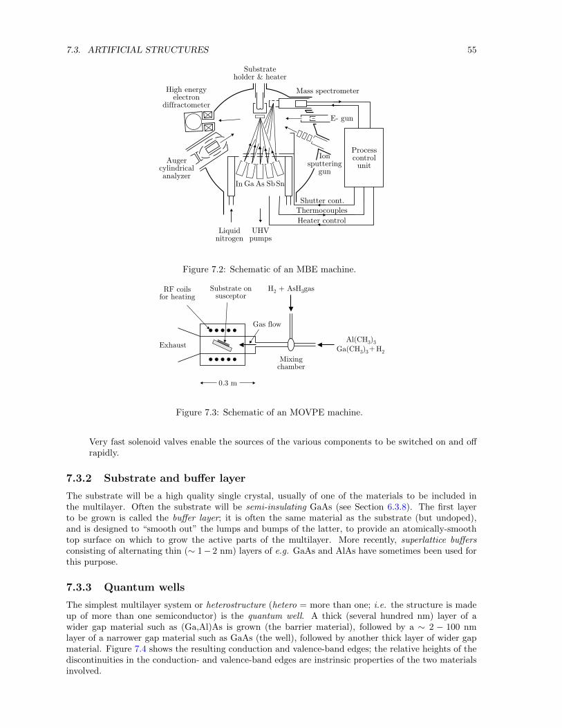
7.3. ARTIFICIAL STRUCTURES 55
Substrateholder & heater
Mass spectrometerHigh energyelectron
diffractometer
Augercylindricalanalyzer
Processcontrolunit
E- gun
Shutter cont.
Thermocouples
Heater control
Liquidnitrogen
UHVpumps
In Ga As SbSn
Ionsputtering
gun
Figure 7.2: Schematic of an MBE machine.
0.3 m
Mixingchamber
Exhaust
Substrate onsusceptor
Gas flow
RF coilsfor heating
H + AsH gas2 3
Al(CH )
Ga(CH ) +H3 3
3 3 2
Figure 7.3: Schematic of an MOVPE machine.
Very fast solenoid valves enable the sources of the various components to be switched on and offrapidly.
7.3.2 Substrate and buffer layer
The substrate will be a high quality single crystal, usually of one of the materials to be included inthe multilayer. Often the substrate will be semi-insulating GaAs (see Section 6.3.8). The first layerto be grown is called the buffer layer; it is often the same material as the substrate (but undoped),and is designed to “smooth out” the lumps and bumps of the latter, to provide an atomically-smoothtop surface on which to grow the active parts of the multilayer. More recently, superlattice buffersconsisting of alternating thin (∼ 1− 2 nm) layers of e.g. GaAs and AlAs have sometimes been used forthis purpose.
7.3.3 Quantum wells
The simplest multilayer system or heterostructure (hetero = more than one; i.e. the structure is madeup of more than one semiconductor) is the quantum well. A thick (several hundred nm) layer of awider gap material such as (Ga,Al)As is grown (the barrier material), followed by a ∼ 2 − 100 nmlayer of a narrower gap material such as GaAs (the well), followed by another thick layer of wider gapmaterial. Figure 7.4 shows the resulting conduction and valence-band edges; the relative heights of thediscontinuities in the conduction- and valence-band edges are instrinsic properties of the two materialsinvolved.
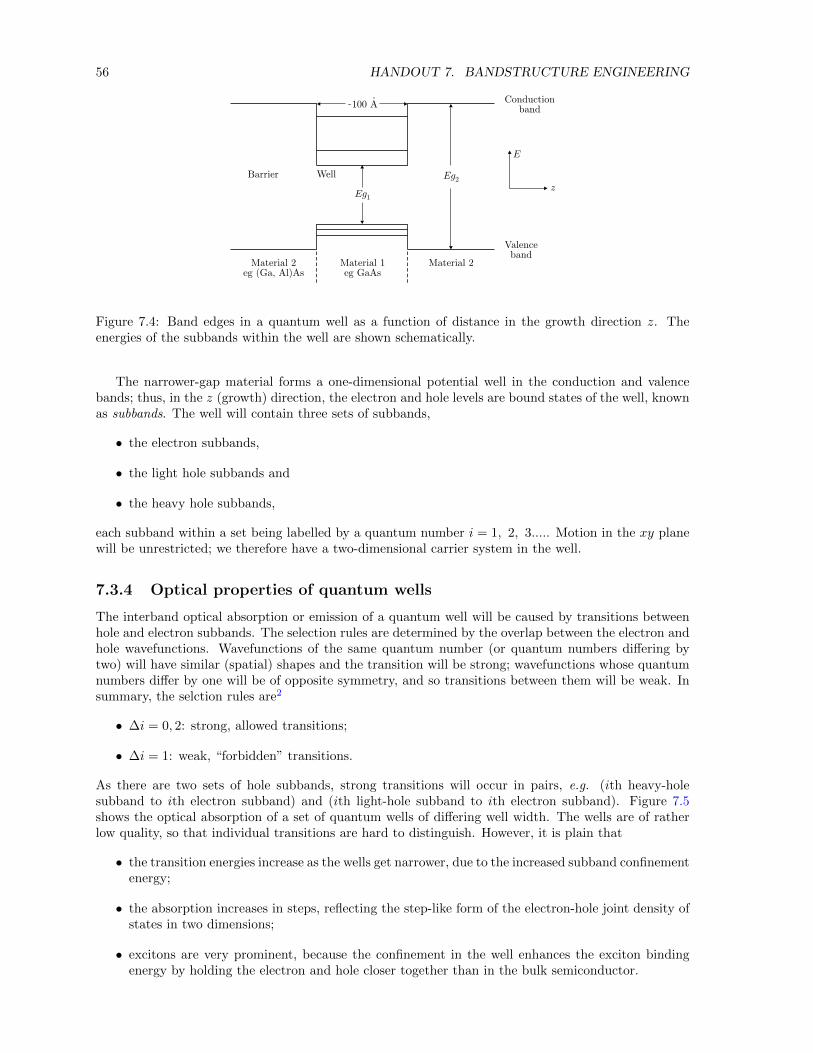
56 HANDOUT 7. BANDSTRUCTURE ENGINEERING
Eg1
Eg2Well
~100 Aº
Barrier
Material 2eg (Ga, Al)As
Material 1eg GaAs
Material 2
Conductionband
E
z
Valenceband
Figure 7.4: Band edges in a quantum well as a function of distance in the growth direction z. Theenergies of the subbands within the well are shown schematically.
The narrower-gap material forms a one-dimensional potential well in the conduction and valencebands; thus, in the z (growth) direction, the electron and hole levels are bound states of the well, knownas subbands. The well will contain three sets of subbands,
• the electron subbands,
• the light hole subbands and
• the heavy hole subbands,
each subband within a set being labelled by a quantum number i = 1, 2, 3..... Motion in the xy planewill be unrestricted; we therefore have a two-dimensional carrier system in the well.
7.3.4 Optical properties of quantum wells
The interband optical absorption or emission of a quantum well will be caused by transitions betweenhole and electron subbands. The selection rules are determined by the overlap between the electron andhole wavefunctions. Wavefunctions of the same quantum number (or quantum numbers differing bytwo) will have similar (spatial) shapes and the transition will be strong; wavefunctions whose quantumnumbers differ by one will be of opposite symmetry, and so transitions between them will be weak. Insummary, the selction rules are2
• ∆i = 0, 2: strong, allowed transitions;
• ∆i = 1: weak, “forbidden” transitions.
As there are two sets of hole subbands, strong transitions will occur in pairs, e.g. (ith heavy-holesubband to ith electron subband) and (ith light-hole subband to ith electron subband). Figure 7.5shows the optical absorption of a set of quantum wells of differing well width. The wells are of ratherlow quality, so that individual transitions are hard to distinguish. However, it is plain that
• the transition energies increase as the wells get narrower, due to the increased subband confinementenergy;
• the absorption increases in steps, reflecting the step-like form of the electron-hole joint density ofstates in two dimensions;
• excitons are very prominent, because the confinement in the well enhances the exciton bindingenergy by holding the electron and hole closer together than in the bulk semiconductor.
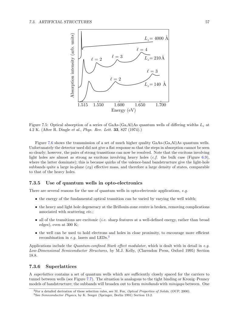
7.3. ARTIFICIAL STRUCTURES 57
1.515 1.550 1.600 1.650 1.700Energy (eV)
Abso
rpti
on inte
nsi
ty (
arb. unit
s)
` = 2` = 3
` = 4
` = 2
` = 3
Lz= 4000 Aº
Lz= 210Aº
Lz= 140 Aº
Figure 7.5: Optical absorption of a series of GaAs-(Ga,Al)As quantum wells of differing widths Lz at4.2 K. (After R. Dingle et al., Phys. Rev. Lett. 33, 827 (1974).)
Figure 7.6 shows the transmission of a set of much higher quality GaAs-(Ga,Al)As quantum wells.Unfortunately the detector used did not give a flat response so that the steps in absorption cannot be seenso clearly; however, the pairs of strong transitions can now be resolved. Note that the excitons involvinglight holes are almost as strong as excitons involving heavy holes (c.f. the bulk case (Figure 6.9),where the latter dominate); this is because quirks of the valence-band bandstructure give the light-holesubbands quite a large in-plane (xy) effective mass, and therefore a large density of states, comparableto that of the heavy holes.
7.3.5 Use of quantum wells in opto-electronics
There are several reasons for the use of quantum wells in opto-electronic applications, e.g.
• the energy of the fundamental optical transition can be varied by varying the well width;
• the heavy and light hole degeneracy at the Brillouin-zone centre is broken, removing complicationsassociated with scattering etc.;
• all of the transitions are excitonic (i.e. sharp features at a well-defined energy, rather than broadedges), even at 300 K;
• the well can be used to hold electrons and holes in close proximity, to encourage more efficientrecombination in e.g. lasers and LEDs.3
Applications include the Quantum-confined Stark effect modulator, which is dealt with in detail in e.g.Low-Dimensional Semiconductor Structures, by M.J. Kelly, (Clarendon Press, Oxford 1995) Section18.8.
7.3.6 Superlattices
A superlattice contains a set of quantum wells which are sufficiently closely spaced for the carriers totunnel between wells (see Figure 7.7). The situation is analogous to the tight binding or Kronig–Penneymodels of bandstructure; the subbands will broaden out to form minibands with minigaps between. One
2For a detailed derivation of these selection rules, see M. Fox, Optical Properties of Solids, (OUP, 2000).3See Semiconductor Physics, by K. Seeger (Springer, Berlin 1991) Section 13.2.
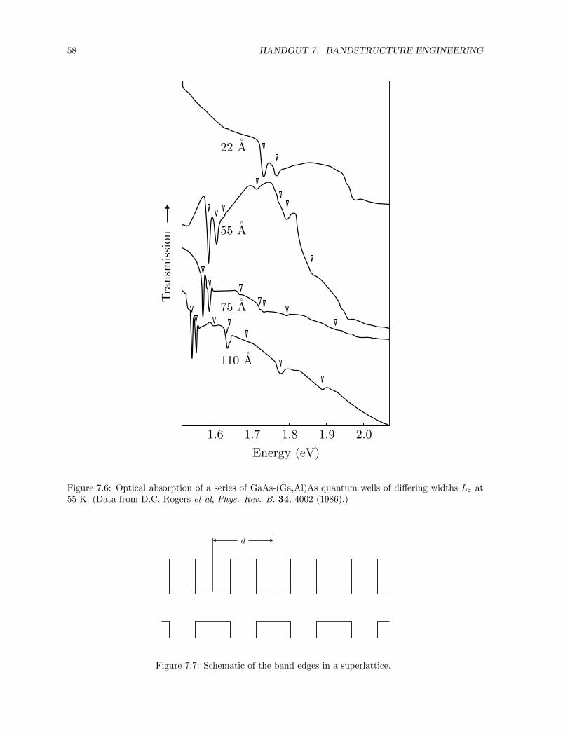
58 HANDOUT 7. BANDSTRUCTURE ENGINEERING
22 Aº
55 Aº
75 Aº
110 Aº
1.6 1.7 1.8 1.9 2.0
Energy (eV)
Tra
nsm
issi
on
Figure 7.6: Optical absorption of a series of GaAs-(Ga,Al)As quantum wells of differing widths Lz at55 K. (Data from D.C. Rogers et al, Phys. Rev. B. 34, 4002 (1986).)
d
Figure 7.7: Schematic of the band edges in a superlattice.
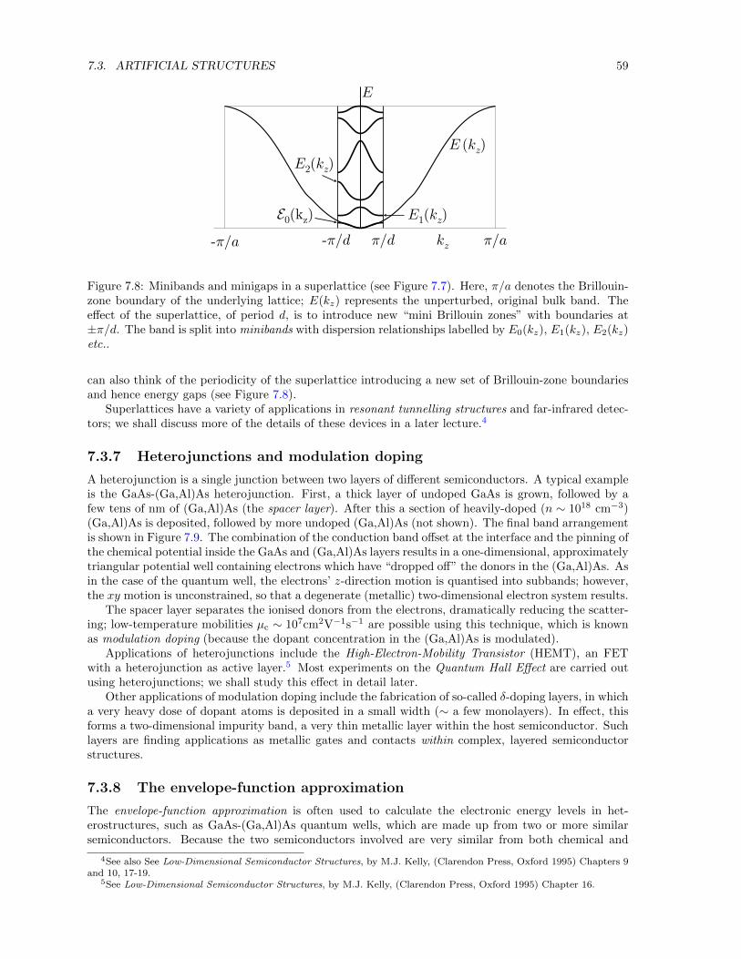
7.3. ARTIFICIAL STRUCTURES 59
E
E k( )z
kz
E k1( )z
E k2( )z
E0 z(k )
- /¼ a - /¼ d ¼ d/ ¼ a/
Figure 7.8: Minibands and minigaps in a superlattice (see Figure 7.7). Here, π/a denotes the Brillouin-zone boundary of the underlying lattice; E(kz) represents the unperturbed, original bulk band. Theeffect of the superlattice, of period d, is to introduce new “mini Brillouin zones” with boundaries at±π/d. The band is split into minibands with dispersion relationships labelled by E0(kz), E1(kz), E2(kz)etc..
can also think of the periodicity of the superlattice introducing a new set of Brillouin-zone boundariesand hence energy gaps (see Figure 7.8).
Superlattices have a variety of applications in resonant tunnelling structures and far-infrared detec-tors; we shall discuss more of the details of these devices in a later lecture.4
7.3.7 Heterojunctions and modulation doping
A heterojunction is a single junction between two layers of different semiconductors. A typical exampleis the GaAs-(Ga,Al)As heterojunction. First, a thick layer of undoped GaAs is grown, followed by afew tens of nm of (Ga,Al)As (the spacer layer). After this a section of heavily-doped (n ∼ 1018 cm−3)(Ga,Al)As is deposited, followed by more undoped (Ga,Al)As (not shown). The final band arrangementis shown in Figure 7.9. The combination of the conduction band offset at the interface and the pinning ofthe chemical potential inside the GaAs and (Ga,Al)As layers results in a one-dimensional, approximatelytriangular potential well containing electrons which have “dropped off” the donors in the (Ga,Al)As. Asin the case of the quantum well, the electrons’ z-direction motion is quantised into subbands; however,the xy motion is unconstrained, so that a degenerate (metallic) two-dimensional electron system results.
The spacer layer separates the ionised donors from the electrons, dramatically reducing the scatter-ing; low-temperature mobilities µc ∼ 107cm2V−1s−1 are possible using this technique, which is knownas modulation doping (because the dopant concentration in the (Ga,Al)As is modulated).
Applications of heterojunctions include the High-Electron-Mobility Transistor (HEMT), an FETwith a heterojunction as active layer.5 Most experiments on the Quantum Hall Effect are carried outusing heterojunctions; we shall study this effect in detail later.
Other applications of modulation doping include the fabrication of so-called δ-doping layers, in whicha very heavy dose of dopant atoms is deposited in a small width (∼ a few monolayers). In effect, thisforms a two-dimensional impurity band, a very thin metallic layer within the host semiconductor. Suchlayers are finding applications as metallic gates and contacts within complex, layered semiconductorstructures.
7.3.8 The envelope-function approximation
The envelope-function approximation is often used to calculate the electronic energy levels in het-erostructures, such as GaAs-(Ga,Al)As quantum wells, which are made up from two or more similarsemiconductors. Because the two semiconductors involved are very similar from both chemical and
4See also See Low-Dimensional Semiconductor Structures, by M.J. Kelly, (Clarendon Press, Oxford 1995) Chapters 9and 10, 17-19.
5See Low-Dimensional Semiconductor Structures, by M.J. Kelly, (Clarendon Press, Oxford 1995) Chapter 16.
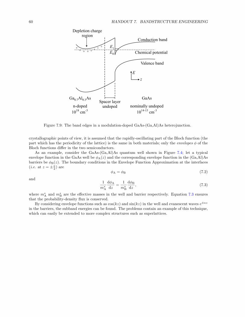
60 HANDOUT 7. BANDSTRUCTURE ENGINEERING
Depletion chargeregion
E1
E0
Conduction band
Chemical potential
Valence band
E
z
Ga Al As0.7 0.3Spacer layer
undoped
GaAs
nominally undoped
10 cm14-15 -3
++ + + + + + +
n-doped
10 cm18 -3
Figure 7.9: The band edges in a modulation-doped GaAs-(Ga,Al)As heterojunction.
crystallographic points of view, it is assumed that the rapidly-oscillating part of the Bloch function (thepart which has the periodicity of the lattice) is the same in both materials; only the envelopes φ of theBloch functions differ in the two semiconductors.
As an example, consider the GaAs-(Ga,Al)As quantum well shown in Figure 7.4; let a typicalenvelope function in the GaAs well be φA(z) and the corresponding envelope function in the (Ga,Al)Asbarriers be φB(z). The boundary conditions in the Envelope Function Approximation at the interfaces(i.e. at z = ±a2 ) are
φA = φB (7.2)
and1
m∗A
dφA
dz=
1
m∗B
dφB
dz, (7.3)
where m∗A and m∗B are the effective masses in the well and barrier respectively. Equation 7.3 ensuresthat the probability-density flux is conserved.
By considering envelope functions such as cos(kz) and sin(kz) in the well and evanescent waves e±κz
in the barriers, the subband energies can be found. The problems contain an example of this technique,which can easily be extended to more complex structures such as superlattices.
Handout 8
Carbon nanotubes
8.1 Introduction
In the last lecture we started to look at bandstructure engineering and the construction of “artificial”materials. In this section we will take a closer look at one particular nanostructure; the carbon nanotube,which is currently the focus of intense research. This system also provides us with an opportunity applymany of the techniques of bandstructure calculation that we have learnt so far.
Carbon nanotubes are single sheets of graphite (called graphene) rolled into cylinders. The diameterof the tubes are typically of nanometer dimensions, while the lengths are typically micrometers. Thishuge aspect ratio leads to unusual electrical transport. Notably some tubes behaving as metals andothers as semiconductors.
The bandstructure of graphite was first calculated by Wallace in 19471, but it was not until 1991that multi-walled nanotubes were discovered2 . We will concentrate on single walled nanotubes whichwere discovered in 1993.
8.2 Reading
Since carbon nanotubes are currently an area of active research the books on the subject tend to beaimed at a research audience. For those of you who would like to read more about carbon nanotubes Ican recommend two books:
1. Physical properties of carbon nanotubes by Saito, Dresselhaus and Dresselhaus (Imperial CollegePress, 1998).
2. Carbon Nanotubes, basic concepts and physical properties by Reich, Thomsen and Maultzsch(Wiley, 2004).
8.3 Lecture slides
The following 7 pages reproduce the slides shown in the lectures.
1See P.R. Wallace Physical Review, 71: 622-634 (1947)2S. Iijima, Nature 354: 56-58 (1991)
61
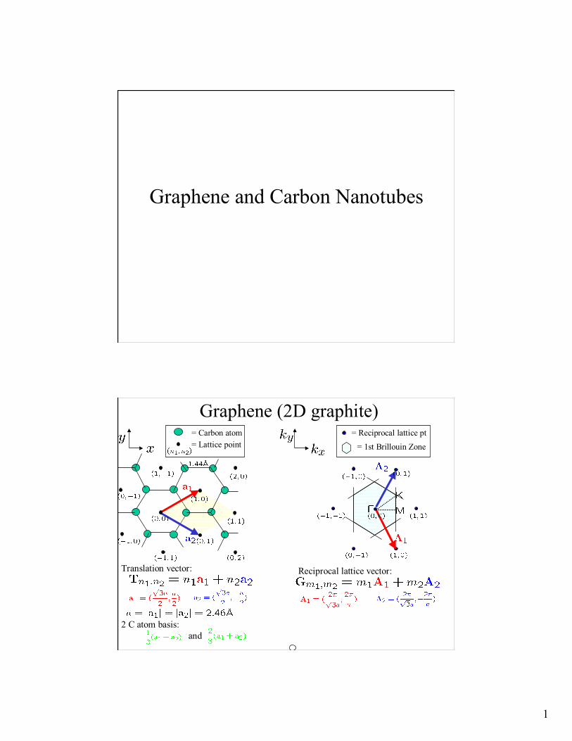
!
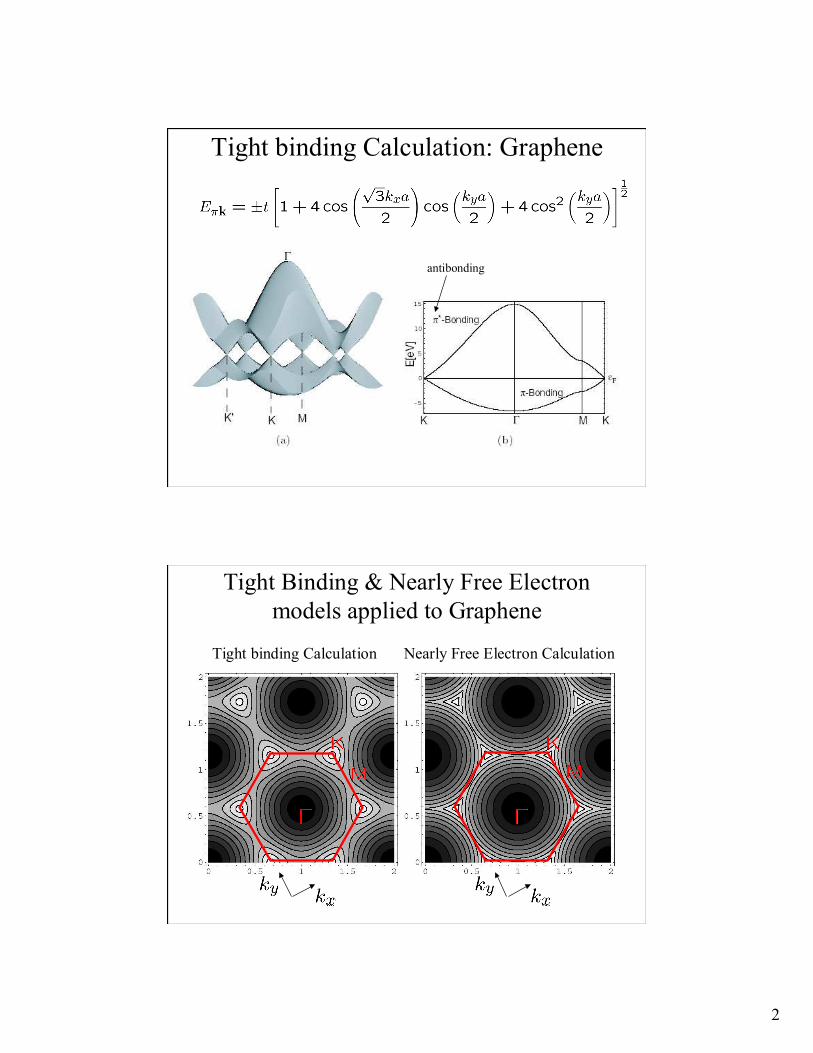
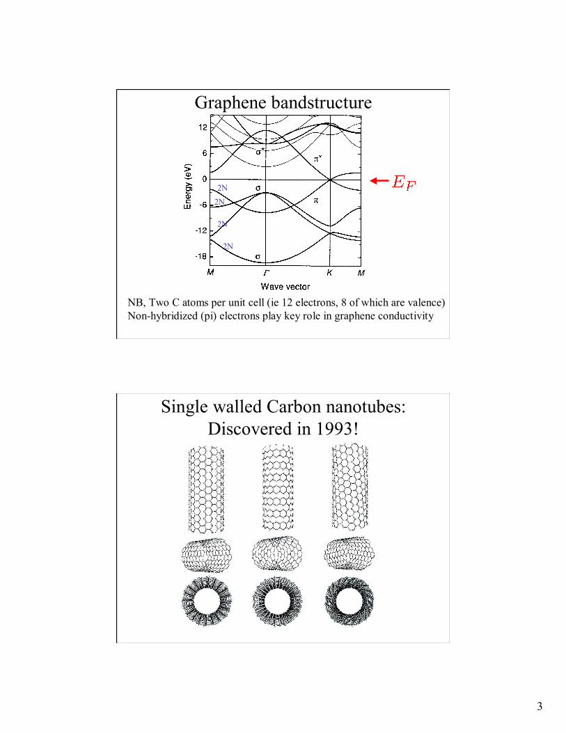
! "#
$
%# &' (()
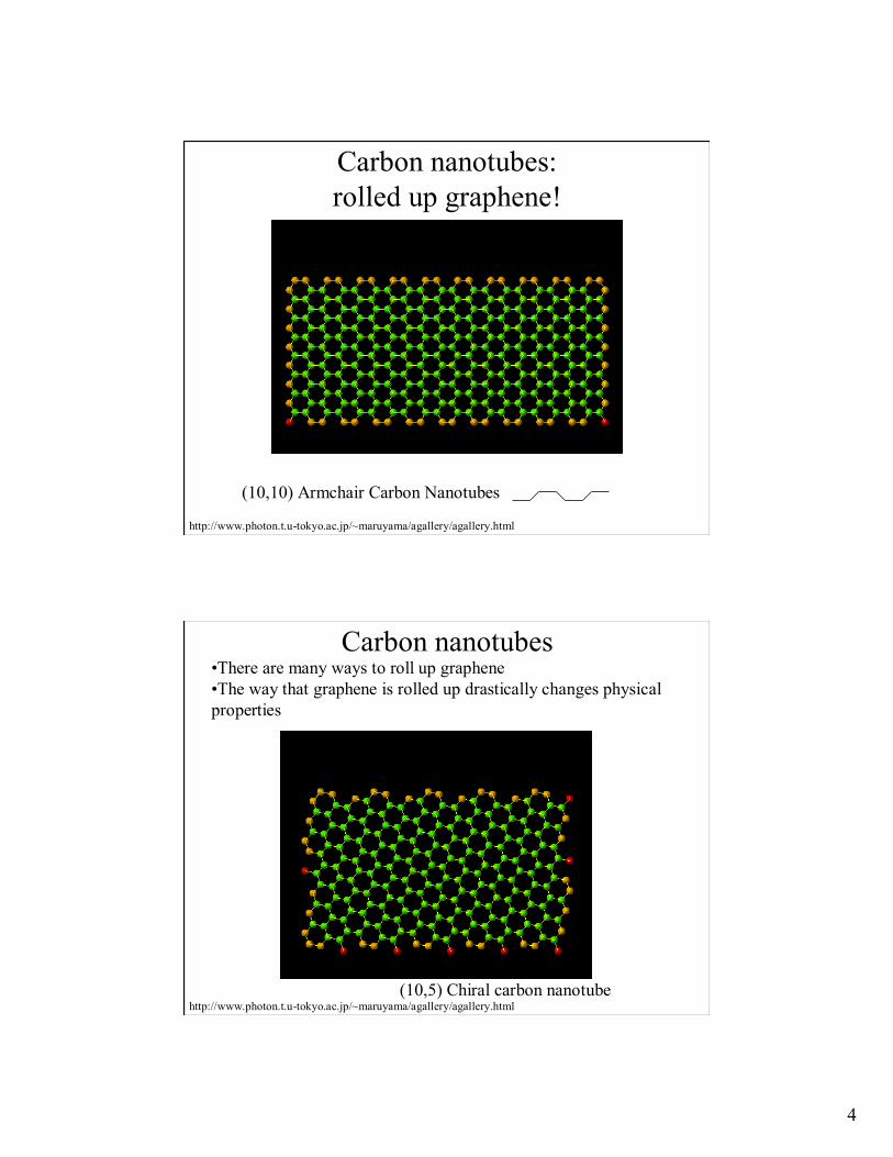
!"#$"""
!"#$"""%
&'""&'" ""

!"#$"%&'%()*# "+
"%,)%%% !
-%",. &-%%%
), !/0 !/0
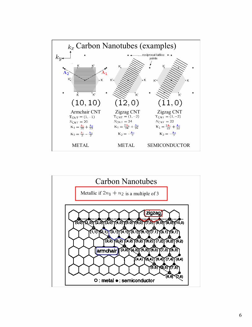
!"
##
!!$ ! !$%
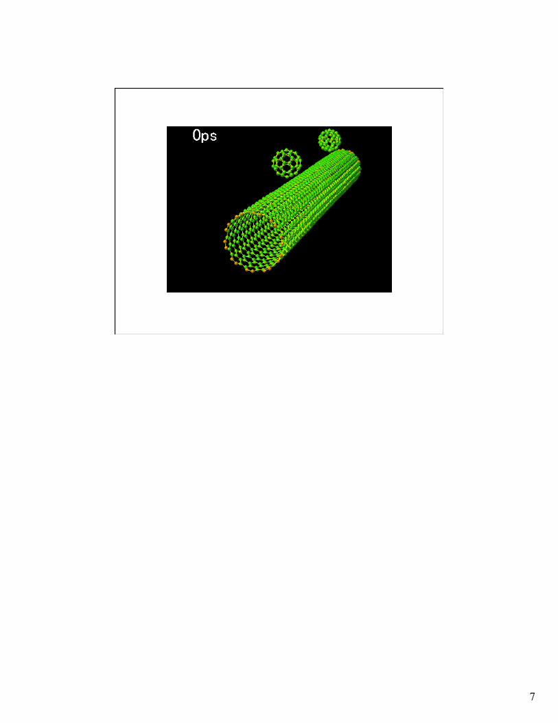

8.3. LECTURE SLIDES 69
Figure 8.1 shows the band gaps
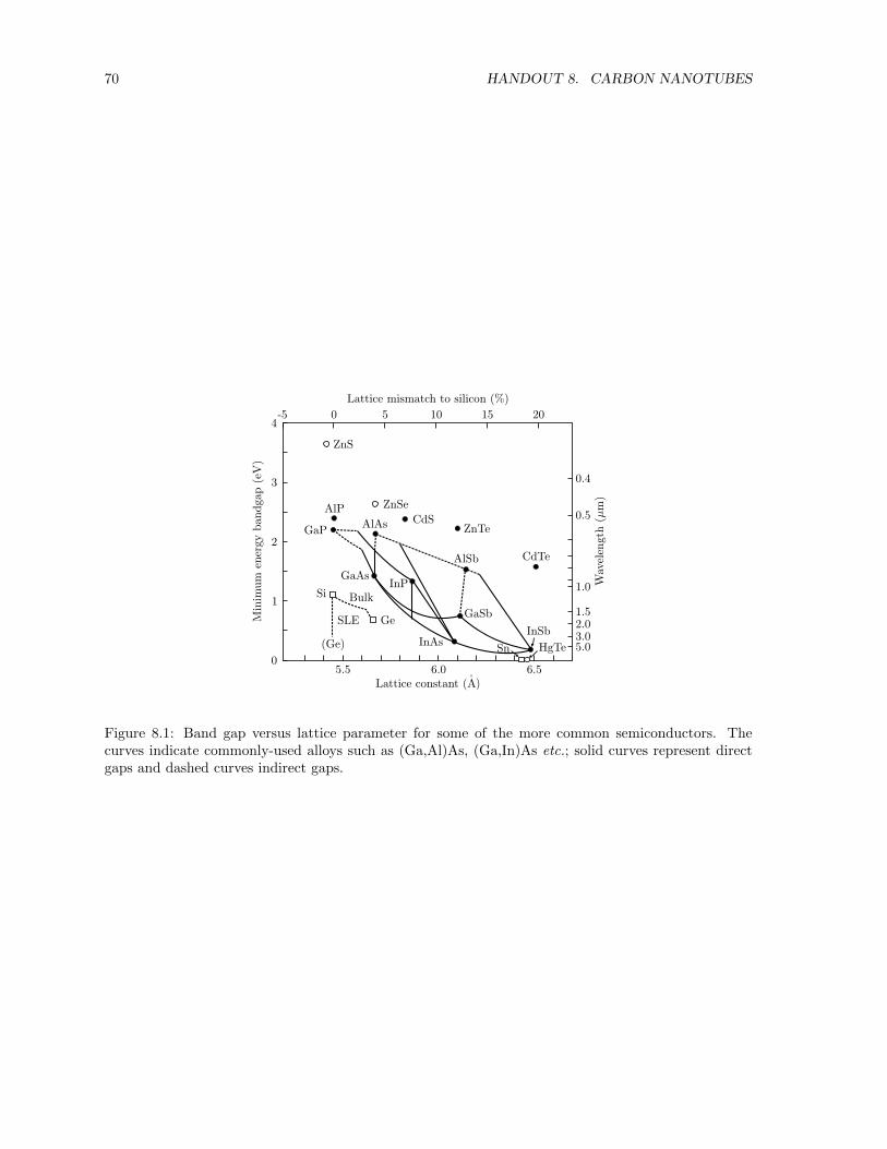
70 HANDOUT 8. CARBON NANOTUBES
5.5 6.0 6.5Lattice constant (Aº)
-5 0 5 10 15 20
0.4
0.5
1.0
1.52.03.05.0
ZnS
AlP ZnSe
AlAs CdSZnTe
AlSb CdTe
GaP
GaAs
GaSb
Si Bulk
SLE Ge
(Ge) InAsInSb
Sn HgTe
InP
4
3
2
1
0
Wav
elen
gth (
m)
¹
Min
imum
ener
gy b
andga
p (
eV)
Lattice mismatch to silicon (%)
Figure 8.1: Band gap versus lattice parameter for some of the more common semiconductors. Thecurves indicate commonly-used alloys such as (Ga,Al)As, (Ga,In)As etc.; solid curves represent directgaps and dashed curves indirect gaps.
Handout 9
Measurement of bandstructure
9.1 Introduction
This Lecture will describe a selection of the most common techniques used to measure the bandstructuresof solids. Many of these techniques involve the use of magnetic fields to partially quantise the electronicmotion; this is known as Landau quantisation or cyclotron motion. I shall therefore treat the motion ofband electrons in some detail before giving brief details of the techniques themselves.
9.2 Lorentz force and orbits
9.2.1 General considerations
Equation 5.9 may be used to calculate the effect of an external magnetic field B on a band electron, i.e.
hdk
dt= −ev ×B, (9.1)
where the right-hand side is the well-known Lorentz force. Equation 9.1 implies that
• the component of k parallel to B is constant;
• as dkdt is perpendicular to v (defined property of the × operation) and as
v =1
h∇kE(k) (9.2)
(see Equation 5.5), dkdt is perpendicular to ∇kE(k). This means that the electron path (orbit) is
one of constant energy. To see this, consider dkdt .∇kE(k) = 0 (because the two are perpendicular);
writing this in components gives ∂kx∂t
∂E∂kx
+∂ky∂t
∂E∂ky
+ ∂kz∂t
∂E∂kz≡ dE
dt from the chain rule. Hence,dEdt = 0.
In k-space, the possible electron orbits are therefore described by the intersections of surfaces of constantenergy with planes perpendicular to B.
9.2.2 The cyclotron frequency
Consider a section of k-space orbit of constant energy E in a plane perpendicular to B (see Figure 9.1).The time t2 − t1 taken to traverse the part of the orbit between k1 to k2 is
t2 − t1 =
∫ t2
t1
dt =
∫ k2
k1
dk
|k|, (9.3)
71
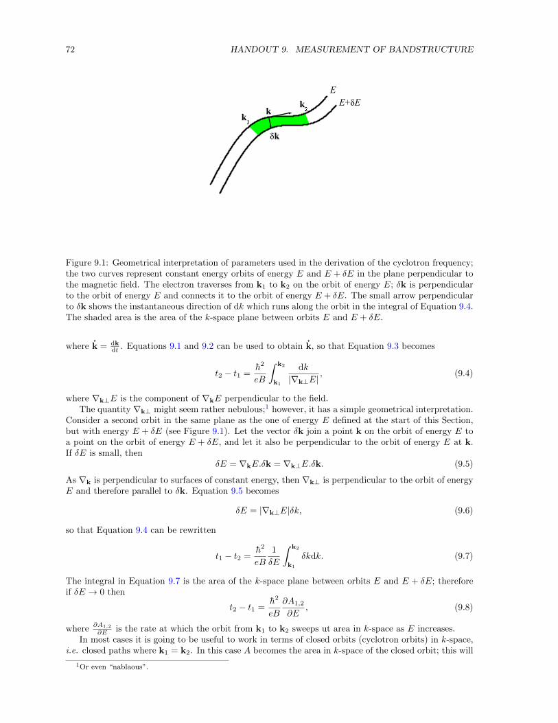
72 HANDOUT 9. MEASUREMENT OF BANDSTRUCTURE
(δ((
δN
NN
N
Figure 9.1: Geometrical interpretation of parameters used in the derivation of the cyclotron frequency;the two curves represent constant energy orbits of energy E and E + δE in the plane perpendicular tothe magnetic field. The electron traverses from k1 to k2 on the orbit of energy E; δk is perpendicularto the orbit of energy E and connects it to the orbit of energy E + δE. The small arrow perpendicularto δk shows the instantaneous direction of dk which runs along the orbit in the integral of Equation 9.4.The shaded area is the area of the k-space plane between orbits E and E + δE.
where k = dkdt . Equations 9.1 and 9.2 can be used to obtain k, so that Equation 9.3 becomes
t2 − t1 =h2
eB
∫ k2
k1
dk
|∇k⊥E|, (9.4)
where ∇k⊥E is the component of ∇kE perpendicular to the field.The quantity ∇k⊥ might seem rather nebulous;1 however, it has a simple geometrical interpretation.
Consider a second orbit in the same plane as the one of energy E defined at the start of this Section,but with energy E + δE (see Figure 9.1). Let the vector δk join a point k on the orbit of energy E toa point on the orbit of energy E + δE, and let it also be perpendicular to the orbit of energy E at k.If δE is small, then
δE = ∇kE.δk = ∇k⊥E.δk. (9.5)
As ∇k is perpendicular to surfaces of constant energy, then ∇k⊥ is perpendicular to the orbit of energyE and therefore parallel to δk. Equation 9.5 becomes
δE = |∇k⊥E|δk, (9.6)
so that Equation 9.4 can be rewritten
t1 − t2 =h2
eB
1
δE
∫ k2
k1
δkdk. (9.7)
The integral in Equation 9.7 is the area of the k-space plane between orbits E and E + δE; thereforeif δE → 0 then
t2 − t1 =h2
eB
∂A1,2
∂E, (9.8)
where∂A1,2
∂E is the rate at which the orbit from k1 to k2 sweeps ut area in k-space as E increases.In most cases it is going to be useful to work in terms of closed orbits (cyclotron orbits) in k-space,
i.e. closed paths where k1 = k2. In this case A becomes the area in k-space of the closed orbit; this will
1Or even “nablaous”.
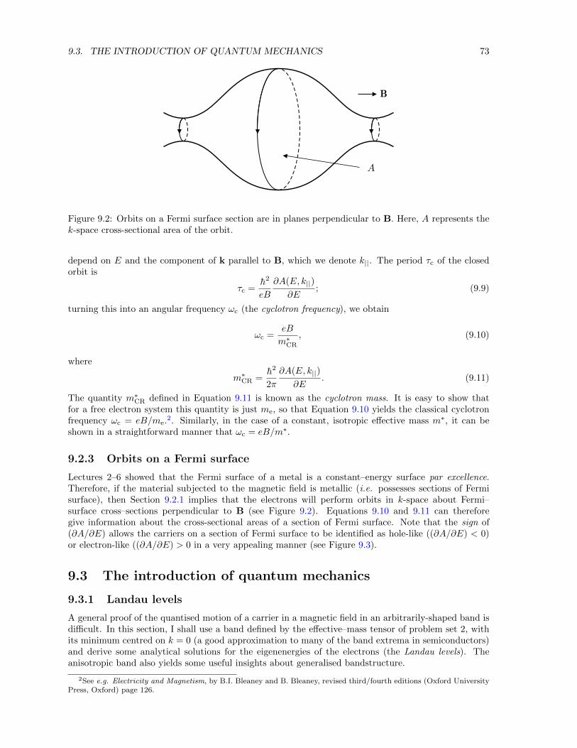
9.3. THE INTRODUCTION OF QUANTUM MECHANICS 73
A
B
Figure 9.2: Orbits on a Fermi surface section are in planes perpendicular to B. Here, A represents thek-space cross-sectional area of the orbit.
depend on E and the component of k parallel to B, which we denote k||. The period τc of the closedorbit is
τc =h2
eB
∂A(E, k||)
∂E; (9.9)
turning this into an angular frequency ωc (the cyclotron frequency), we obtain
ωc =eB
m∗CR
, (9.10)
where
m∗CR =h2
2π
∂A(E, k||)
∂E. (9.11)
The quantity m∗CR defined in Equation 9.11 is known as the cyclotron mass. It is easy to show thatfor a free electron system this quantity is just me, so that Equation 9.10 yields the classical cyclotronfrequency ωc = eB/me.2. Similarly, in the case of a constant, isotropic effective mass m∗, it can beshown in a straightforward manner that ωc = eB/m∗.
9.2.3 Orbits on a Fermi surface
Lectures 2–6 showed that the Fermi surface of a metal is a constant–energy surface par excellence.Therefore, if the material subjected to the magnetic field is metallic (i.e. possesses sections of Fermisurface), then Section 9.2.1 implies that the electrons will perform orbits in k-space about Fermi–surface cross–sections perpendicular to B (see Figure 9.2). Equations 9.10 and 9.11 can thereforegive information about the cross-sectional areas of a section of Fermi surface. Note that the sign of(∂A/∂E) allows the carriers on a section of Fermi surface to be identified as hole-like ((∂A/∂E) < 0)or electron-like ((∂A/∂E) > 0 in a very appealing manner (see Figure 9.3).
9.3 The introduction of quantum mechanics
9.3.1 Landau levels
A general proof of the quantised motion of a carrier in a magnetic field in an arbitrarily-shaped band isdifficult. In this section, I shall use a band defined by the effective–mass tensor of problem set 2, withits minimum centred on k = 0 (a good approximation to many of the band extrema in semiconductors)and derive some analytical solutions for the eigenenergies of the electrons (the Landau levels). Theanisotropic band also yields some useful insights about generalised bandstructure.
2See e.g. Electricity and Magnetism, by B.I. Bleaney and B. Bleaney, revised third/fourth editions (Oxford UniversityPress, Oxford) page 126.
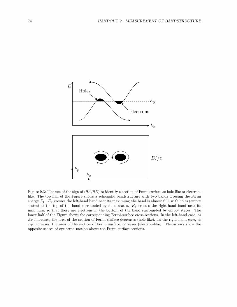
74 HANDOUT 9. MEASUREMENT OF BANDSTRUCTURE
Holes
Electrons
ky
kx
kx
B z//
E
EF
Figure 9.3: The use of the sign of (∂A/∂E) to identify a section of Fermi surface as hole-like or electron-like. The top half of the Figure shows a schematic bandstructure with two bands crossing the Fermienergy EF. EF crosses the left-hand band near its maximum; the band is almost full, with holes (emptystates) at the top of the band surrounded by filled states. EF crosses the right-hand band near itsminimum, so that there are electrons in the bottom of the band surrounded by empty states. Thelower half of the Figure shows the corresponding Fermi-surface cross-sections. In the left-hand case, asEF increases, the area of the section of Fermi surface decreases (hole-like). In the right-hand case, asEF increases, the area of the section of Fermi surface increases (electron-like). The arrows show theopposite senses of cyclotron motion about the Fermi-surface sections.
9.3. THE INTRODUCTION OF QUANTUM MECHANICS 75
For further generality, Section 9.3.2 will derive the Landau quantisation of arbitrarily-shaped bandsin the limit that hωc EF.
The Hamiltonian for electrons in the band defined by the effective mass tensor of problem set 2,with its minimum centred on k = 0 is
Pxe1
(2m1)12
+Pye2
(2m2)12
+Pze3
(2m3)12
2
ψ = Eψ, (9.12)
where the P are one-dimensional momentum operators; i.e. all of the effects of the crystalline potentialhave been absorbed into the bandstructure, which is defined by the effective masses. Substitution of aplane wave solution into Equation 9.12 yields energies of the correct form, i.e.
E =h2k2
x
2m1+h2k2
y
2m2+h2k2
z
2m3. (9.13)
Consider a magnetic field B directed along the z (e3) axis. In addition, remember that B = ∇×A,where A is the magnetic vector potential. One particular A which gives the correct B is
A = (0, Bx, 0); (9.14)
this choice is known as the Landau gauge. For an electron in a magnetic field,
P → (P + eA). (9.15)
Making such a substitution into Equation 9.12 givesPxe1
(2m1)12
+(Py + eBx)e2
(2m2)12
+Pze3
(2m3)12
2
ψ = Eψ. (9.16)
All that we have done is introduce an extra term with x in it; as [Py, x] = [Pz, x] = 0.3 Py and Pz stillcommute with the Hamiltonian; their associated physical quantities are thus constants of the motion.The operators Py and Pz in Equation 9.16 can therefore be replaced by their constant values hky andhkz respectively. Equation 9.16 becomes
Pxe1
(2m1)12
+(hky + eBx)e2
(2m2)12
+hkze3
(2m3)12
2
ψ = Eψ. (9.17)
Squaring the bracket, remembering that the Cartesian unit vectors ej are mutually perpendicular (i.e.ej .el = δj,l), gives
P2x
2m1+
(hky + eBx)2
2m2+h2k2
z
2m3
ψ = Eψ. (9.18)
Making the substitutions E′ = E − (h2k2z/2m3) and x0 = −(hky/eB), and rearranging yields
P2x
2m1+e2B2
2m2(x− x0)2ψ = E′ψ. (9.19)
Equation 9.19 looks exactly like the Hamiltonian of a one-dimensional harmonic oscillator, i.e.,
P2x
2m+
1
2mω2(x− x0)2ψ = E′ψ, (9.20)
with ω = eB/(m1m2)12 ; thus E′ = (l+ 1
2 )hω, with l = 0, 1, 2, 3..... The energy levels of the electron aretherefore
E(l, B, kz) =h2k2
z
2m3+ (l +
1
2)hω, (9.21)
3These are standard commutation relationships; see e.g. Quantum Mechanics, by Stephen Gasiorowicz (Wiley, NewYork 1974) pages 51, 141.
76 HANDOUT 9. MEASUREMENT OF BANDSTRUCTURE
with
ω = eB/(m1m2)12 ≡ ωc. (9.22)
The equivalence of ω and ωc, the cyclotron frequency for this geometry (i.e. ωc = eB/m∗CR, with
m∗CR = h2
2π
∂A(E,k||)
∂E ), is left to the reader.
The following points may be deduced from Equation 9.21.
• The energy of the electron’s motion in the plane perpendicular to B is completely quantised.These quantised levels are known as Landau levels.
• The k-space areas of the orbits in the plane perpendicular to B are also quantised (this is easyto work out in the present case and is left as an exercise); thus, allowed orbits fall on “Landautubes” in k-space with quantised cross-sectional area.
• The energy “quantum” for the in-plane motion appears to be h×(the semiclassical cyclotronfrequency).
• The motion parallel to B is unaffected (c.f. Section 9.2.1).
We shall consider the second point in more detail (and more generally) in the following section.
9.3.2 Application of Bohr’s correspondence principle to arbitrarily-shapedFermi surfaces in a magnetic field
In Section 9.4 below we are going to consider the effect of the quantisation of the k-space orbits causedby B on the Fermi surfaces of metals; i.e. we shall be dealing with Landau levels which cut the Fermisurface. The Fermi surfaces of real metals are in general not as simple as the case dealt with in theprevious section. Therefore, in order to treat an arbitrily-shaped band, resulting in an arbitrarily-shaped Fermi surface, we shall use Bohr’s correspondence principle, which states in this context thatthe difference in energy of two adjacent levels is h times the angular frequency of classical motion atthe energy of the levels.
The correspondence principle is only valid for levels with very large quantum numbers. However,this is not really a problem, as we are going to be dealing with Landau levels with energies comparableto EF; in most metals EF is ∼several eV, whereas the cyclotron energy of free electrons is heB/me ≈1.16 × 10⁻⁴ eV at B = 1 T. Laboratory fields are usually ∼ 10 T, and so the quantum numbers ofLandau levels with energies ∼ EF will be l ∼ 104; the correspondence principle should work reasonablywell.
The classical frequency at the energy of interest (i.e. EF) is given by Equation 9.10
ωc =eB
m∗CR
, (9.23)
with m∗CR given by Equation 9.11 as follows
m∗CR =h2
2π
∂A(E, k||)
∂E. (9.24)
Here, A is now specifically the cross-sectional area of the Fermi surface in a plane perpendicular to B.Thus, the separation in energy of two Landau tubes with energies close to EF is
E(l + 1, B, k||)− E(l, B, k||) =heB
m∗CR
, (9.25)
with m∗CR defined by Equation 9.24. (It is interesting to compare this Equation with Equation 9.21.)
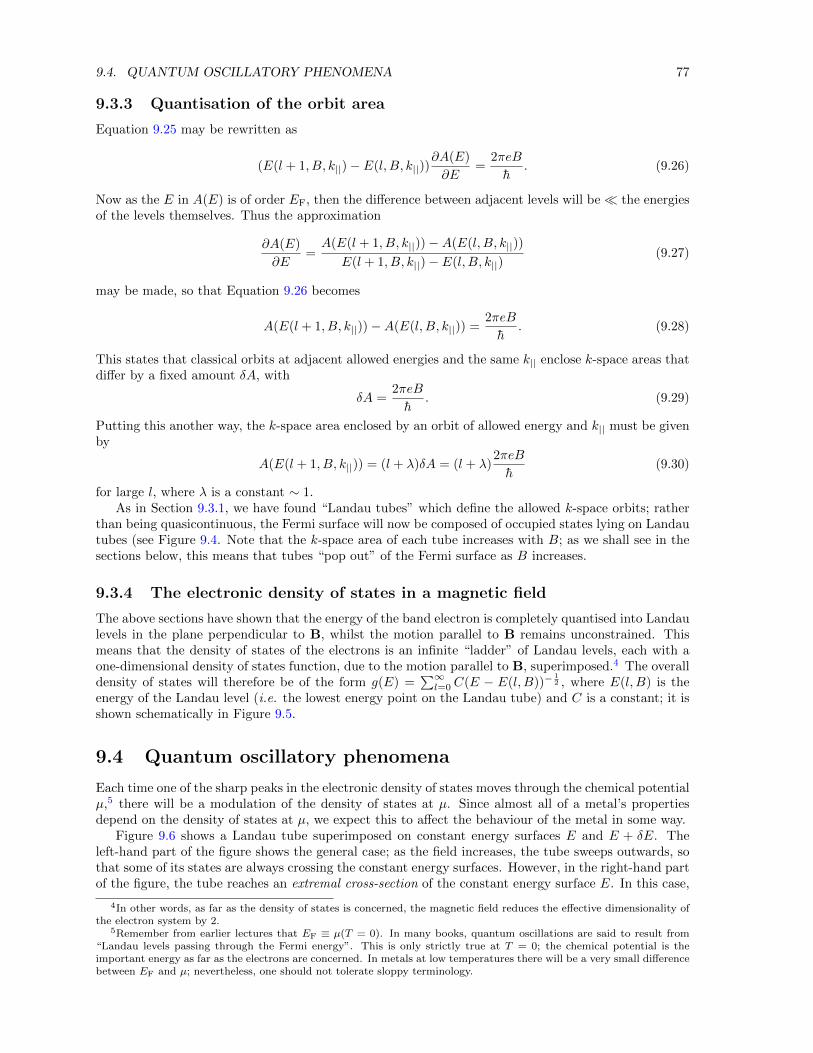
9.4. QUANTUM OSCILLATORY PHENOMENA 77
9.3.3 Quantisation of the orbit area
Equation 9.25 may be rewritten as
(E(l + 1, B, k||)− E(l, B, k||))∂A(E)
∂E=
2πeB
h. (9.26)
Now as the E in A(E) is of order EF, then the difference between adjacent levels will be the energiesof the levels themselves. Thus the approximation
∂A(E)
∂E=A(E(l + 1, B, k||))−A(E(l, B, k||))
E(l + 1, B, k||)− E(l, B, k||)(9.27)
may be made, so that Equation 9.26 becomes
A(E(l + 1, B, k||))−A(E(l, B, k||)) =2πeB
h. (9.28)
This states that classical orbits at adjacent allowed energies and the same k|| enclose k-space areas thatdiffer by a fixed amount δA, with
δA =2πeB
h. (9.29)
Putting this another way, the k-space area enclosed by an orbit of allowed energy and k|| must be givenby
A(E(l + 1, B, k||)) = (l + λ)δA = (l + λ)2πeB
h(9.30)
for large l, where λ is a constant ∼ 1.As in Section 9.3.1, we have found “Landau tubes” which define the allowed k-space orbits; rather
than being quasicontinuous, the Fermi surface will now be composed of occupied states lying on Landautubes (see Figure 9.4. Note that the k-space area of each tube increases with B; as we shall see in thesections below, this means that tubes “pop out” of the Fermi surface as B increases.
9.3.4 The electronic density of states in a magnetic field
The above sections have shown that the energy of the band electron is completely quantised into Landaulevels in the plane perpendicular to B, whilst the motion parallel to B remains unconstrained. Thismeans that the density of states of the electrons is an infinite “ladder” of Landau levels, each with aone-dimensional density of states function, due to the motion parallel to B, superimposed.4 The overalldensity of states will therefore be of the form g(E) =
∑∞l=0 C(E − E(l, B))−
12 , where E(l, B) is the
energy of the Landau level (i.e. the lowest energy point on the Landau tube) and C is a constant; it isshown schematically in Figure 9.5.
9.4 Quantum oscillatory phenomena
Each time one of the sharp peaks in the electronic density of states moves through the chemical potentialµ,5 there will be a modulation of the density of states at µ. Since almost all of a metal’s propertiesdepend on the density of states at µ, we expect this to affect the behaviour of the metal in some way.
Figure 9.6 shows a Landau tube superimposed on constant energy surfaces E and E + δE. Theleft-hand part of the figure shows the general case; as the field increases, the tube sweeps outwards, sothat some of its states are always crossing the constant energy surfaces. However, in the right-hand partof the figure, the tube reaches an extremal cross-section of the constant energy surface E. In this case,
4In other words, as far as the density of states is concerned, the magnetic field reduces the effective dimensionality ofthe electron system by 2.
5Remember from earlier lectures that EF ≡ µ(T = 0). In many books, quantum oscillations are said to result from“Landau levels passing through the Fermi energy”. This is only strictly true at T = 0; the chemical potential is theimportant energy as far as the electrons are concerned. In metals at low temperatures there will be a very small differencebetween EF and µ; nevertheless, one should not tolerate sloppy terminology.
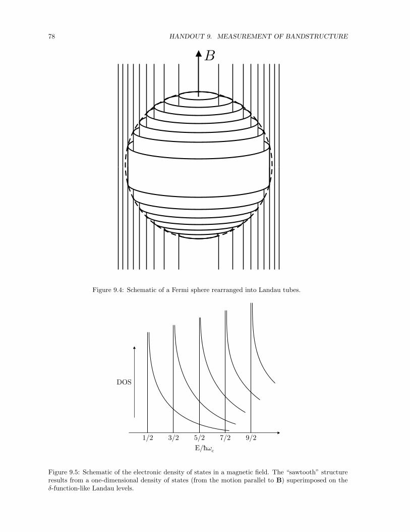
78 HANDOUT 9. MEASUREMENT OF BANDSTRUCTURE
Figure 9.4: Schematic of a Fermi sphere rearranged into Landau tubes.
Figure 9.5: Schematic of the electronic density of states in a magnetic field. The “sawtooth” structureresults from a one-dimensional density of states (from the motion parallel to B) superimposed on theδ-function-like Landau levels.
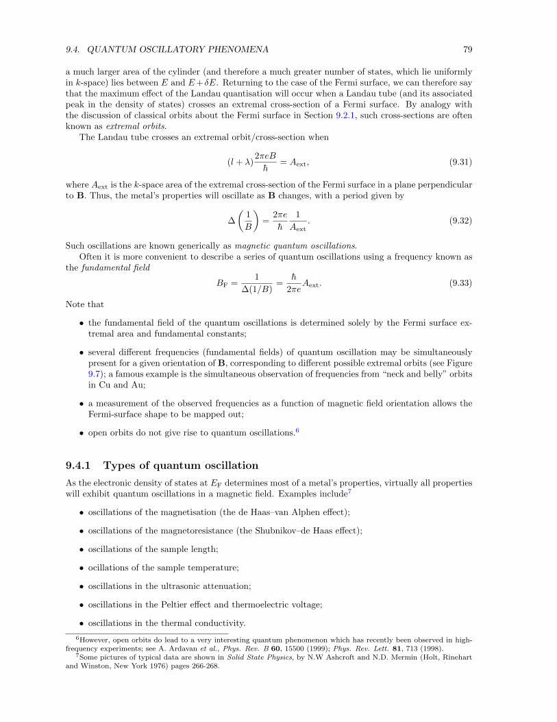
9.4. QUANTUM OSCILLATORY PHENOMENA 79
a much larger area of the cylinder (and therefore a much greater number of states, which lie uniformlyin k-space) lies between E and E+δE. Returning to the case of the Fermi surface, we can therefore saythat the maximum effect of the Landau quantisation will occur when a Landau tube (and its associatedpeak in the density of states) crosses an extremal cross-section of a Fermi surface. By analogy withthe discussion of classical orbits about the Fermi surface in Section 9.2.1, such cross-sections are oftenknown as extremal orbits.
The Landau tube crosses an extremal orbit/cross-section when
(l + λ)2πeB
h= Aext, (9.31)
where Aext is the k-space area of the extremal cross-section of the Fermi surface in a plane perpendicularto B. Thus, the metal’s properties will oscillate as B changes, with a period given by
∆
(1
B
)=
2πe
h
1
Aext. (9.32)
Such oscillations are known generically as magnetic quantum oscillations.Often it is more convenient to describe a series of quantum oscillations using a frequency known as
the fundamental field
BF =1
∆(1/B)=
h
2πeAext. (9.33)
Note that
• the fundamental field of the quantum oscillations is determined solely by the Fermi surface ex-tremal area and fundamental constants;
• several different frequencies (fundamental fields) of quantum oscillation may be simultaneouslypresent for a given orientation of B, corresponding to different possible extremal orbits (see Figure9.7); a famous example is the simultaneous observation of frequencies from “neck and belly” orbitsin Cu and Au;
• a measurement of the observed frequencies as a function of magnetic field orientation allows theFermi-surface shape to be mapped out;
• open orbits do not give rise to quantum oscillations.6
9.4.1 Types of quantum oscillation
As the electronic density of states at EF determines most of a metal’s properties, virtually all propertieswill exhibit quantum oscillations in a magnetic field. Examples include7
• oscillations of the magnetisation (the de Haas–van Alphen effect);
• oscillations of the magnetoresistance (the Shubnikov–de Haas effect);
• oscillations of the sample length;
• ocillations of the sample temperature;
• oscillations in the ultrasonic attenuation;
• oscillations in the Peltier effect and thermoelectric voltage;
• oscillations in the thermal conductivity.
6However, open orbits do lead to a very interesting quantum phenomenon which has recently been observed in high-frequency experiments; see A. Ardavan et al., Phys. Rev. B 60, 15500 (1999); Phys. Rev. Lett. 81, 713 (1998).
7Some pictures of typical data are shown in Solid State Physics, by N.W Ashcroft and N.D. Mermin (Holt, Rinehartand Winston, New York 1976) pages 266-268.
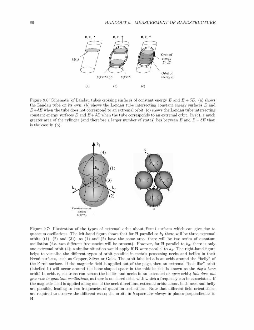
80 HANDOUT 9. MEASUREMENT OF BANDSTRUCTURE
B, kzB, kz B, kz
E k E E( )= +d E k E( )=
Orbit ofenergy
+dE E
Orbit ofenergy E
E k( )z
(a) (b) (c)
Figure 9.6: Schematic of Landau tubes crossing surfaces of constant energy E and E + δE. (a) showsthe Landau tube on its own; (b) shows the Landau tube intersecting constant energy surfaces E andE+δE when the tube does not correspond to an extremal orbit; (c) shows the Landau tube intersectingconstant energy surfaces E and E+ δE when the tube corresponds to an extremal orbit. In (c), a muchgreater area of the cylinder (and therefore a larger number of states) lies between E and E + δE thanis the case in (b).
Constant-energysurface( )=E k EF
k1
k2
k0
k3
(1)
(2)
(4)
(3)
c
b
a
Figure 9.7: Illustration of the types of extremal orbit about Fermi surfaces which can give rise toquantum oscillations. The left-hand figure shows that for B parallel to k1 there will be three extremalorbits ((1), (2) and (3)); as (1) and (2) have the same area, there will be two series of quantumoscillation (i.e. two different frequencies will be present). However, for B parallel to k2, there is onlyone extremal orbit (4); a similar situation would apply if B were parallel to k3. The right-hand figurehelps to visualise the different types of orbit possible in metals possessing necks and bellies in theirFermi surfaces, such as Copper, Silver or Gold. The orbit labelled a is an orbit around the “belly” ofthe Fermi surface. If the magnetic field is applied out of the page, then an extremal “hole-like” orbit(labelled b) will occur around the bone-shaped space in the middle; this is known as the dog’s boneorbit! In orbit c, electrons run across the bellies and necks in an extended or open orbit; this does notgive rise to quantum oscillations, as there is no closed orbit with which a frequency can be associated. Ifthe magnetic field is applied along one of the neck directions, extremal orbits about both neck and bellyare possible, leading to two frequencies of quantum oscillations. Note that different field orientationsare required to observe the different cases; the orbits in k-space are always in planes perpendicular toB.
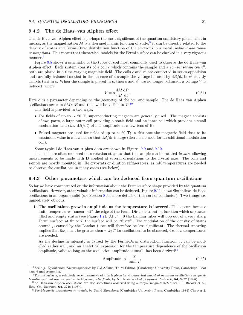
9.4. QUANTUM OSCILLATORY PHENOMENA 81
9.4.2 The de Haas–van Alphen effect
The de Haas-van Alphen effect is perhaps the most significant of the quantum oscillatory phenomena inmetals; as the magnetisation M is a thermodynamic function of state;8 it can be directly related to thedensity of states and Fermi–Dirac distribution function of the electrons in a metal, without additionalassumptions. This means that theoretical models for the Fermi surface can be checked in a very rigorousmanner.9
Figure 9.8 shows a schematic of the types of coil most commonly used to observe the de Haas–vanAlphen effect. Each system consists of a coil c which contains the sample and a compensating coil c0;both are placed in a time-varying magnetic field. The coils c and c0 are connected in series-oppositionand carefully balanced so that in the absence of a sample the voltage induced by dB/dt in c0 exactlycancels that in c. When the sample is placed in c, then c and c0 are no longer balanced; a voltage V isinduced, where
V = αdM
dB
dB
dt. (9.34)
Here α is a parameter depending on the geometry of the coil and sample. The de Haas–van Alphenoscillations occur in dM/dB and thus will be visible in V .10
The field is provided in two ways.
• For fields of up to ∼ 20 T, superconducting magnets are generally used. The magnet consistsof two parts, a large outer coil providing a static field and an inner coil which provides a smallmodulation field (i.e. dB/dt) of mT amplitude at a few tens of Hz.
• Pulsed magnets are used for fields of up to ∼ 60 T; in this case the magnetic field rises to itsmaximum value in a few ms, so that dB/dt is large (there is no need for an additional modulationcoil).
Some typical de Haas-van Alphen data are shown in Figures 9.9 and 9.10.The coils are often mounted on a rotation stage so that the sample can be rotated in situ, allowing
measurements to be made with B applied at several orientations to the crystal axes. The coils andsample are mostly mounted in 3He cryostats or dilution refrigerators, as mK temperatures are neededto observe the oscillations in many cases (see below).
9.4.3 Other parameters which can be deduced from quantum oscillations
So far we have concentrated on the information about the Fermi-surface shape provided by the quantumoscillations. However, other valuable information can be deduced. Figure 9.11 shows Shubnikov–de Haasoscillations in an organic solid (see Section 8 for more details of this sort of conductor). Two things areimmediately obvious.
1. The oscillations grow in amplitude as the temperature is lowered. This occurs becausefinite temperatures “smear out” the edge of the Fermi-Dirac distribution function which separatesfilled and empty states (see Figure 1.7). At T = 0 the Landau tubes will pop out of a very sharpFermi surface; at finite T the surface will be “fuzzy”. The modulation of the density of statesaround µ caused by the Landau tubes will therefore be less significant. The thermal smearingimplies that hωc must be greater than ∼ kBT for oscillations to be observed, i.e. low temperaturesare needed.
As the decline in intensity is caused by the Fermi-Dirac distribution function, it can be mod-elled rather well, and an analytical expression for the temperature dependence of the oscillationamplitude, valid as long as the oscillation amplitude is small, has been derived11
Amplitude ∝ χ
sinhχ, (9.35)
8See e.g. Equilibrium Thermodynamics by C.J Adkins, Third Edition (Cambridge University Press, Cambridge 1983)page 6 and Appendix.
9For enthusiasts, a relatively recent example of this is given in A numerical model of quantum oscillations in quasi-two-dimensional organic metals in high magnetic fields, by N. Harrison et al., Physical Review B, 54, 9977 (1996).
10de Haas-van Alphen oscillations are also sometimes observed using a torque magnetometer; see J.S. Brooks et al.,Rev. Sci. Instrum. 64, 3248 (1987).
11See Magnetic oscillations in metals, by David Shoenberg (Cambridge University Press, Cambridge 1984) Chapter 2.
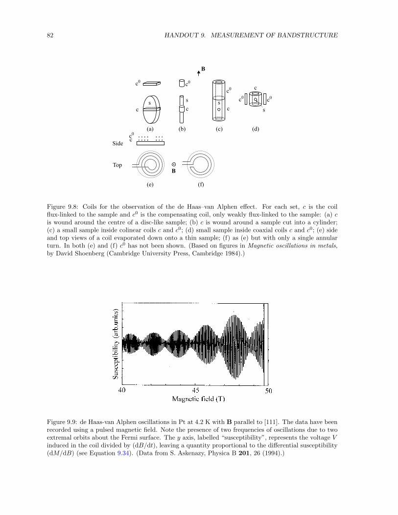
82 HANDOUT 9. MEASUREMENT OF BANDSTRUCTURE
s
ss s
c0c0
c0
c0
c0
c
c0
ccc
c
(c) (d)(b)(a)
B
B
(e) (f)
Side
Top
Figure 9.8: Coils for the observation of the de Haas–van Alphen effect. For each set, c is the coilflux-linked to the sample and c0 is the compensating coil, only weakly flux-linked to the sample: (a) cis wound around the centre of a disc-like sample; (b) c is wound around a sample cut into a cylinder;(c) a small sample inside colinear coils c and c0; (d) small sample inside coaxial coils c and c0; (e) sideand top views of a coil evaporated down onto a thin sample; (f) as (e) but with only a single annularturn. In both (e) and (f) c0 has not been shown. (Based on figures in Magnetic oscillations in metals,by David Shoenberg (Cambridge University Press, Cambridge 1984).)
Figure 9.9: de Haas-van Alphen oscillations in Pt at 4.2 K with B parallel to [111]. The data have beenrecorded using a pulsed magnetic field. Note the presence of two frequencies of oscillations due to twoextremal orbits about the Fermi surface. The y axis, labelled “susceptibility”, represents the voltage Vinduced in the coil divided by (dB/dt), leaving a quantity proportional to the differential susceptibility(dM/dB) (see Equation 9.34). (Data from S. Askenazy, Physica B 201, 26 (1994).)
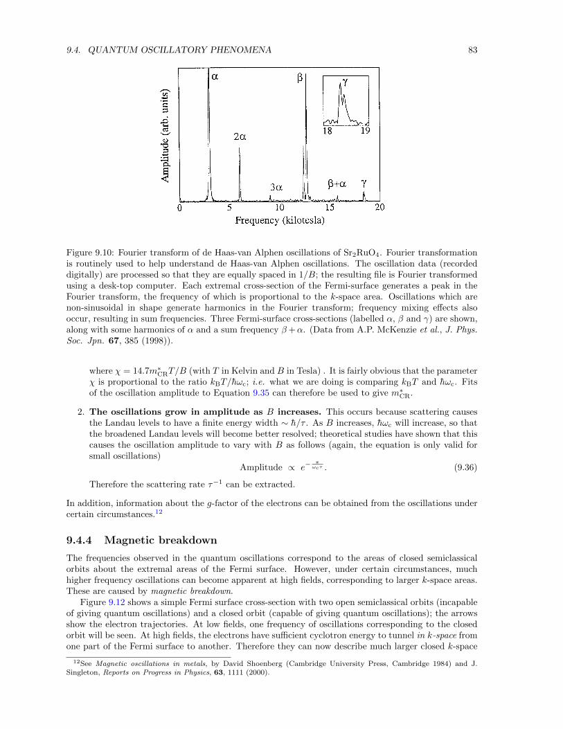
9.4. QUANTUM OSCILLATORY PHENOMENA 83
Figure 9.10: Fourier transform of de Haas-van Alphen oscillations of Sr2RuO4. Fourier transformationis routinely used to help understand de Haas-van Alphen oscillations. The oscillation data (recordeddigitally) are processed so that they are equally spaced in 1/B; the resulting file is Fourier transformedusing a desk-top computer. Each extremal cross-section of the Fermi-surface generates a peak in theFourier transform, the frequency of which is proportional to the k-space area. Oscillations which arenon-sinusoidal in shape generate harmonics in the Fourier transform; frequency mixing effects alsooccur, resulting in sum frequencies. Three Fermi-surface cross-sections (labelled α, β and γ) are shown,along with some harmonics of α and a sum frequency β+α. (Data from A.P. McKenzie et al., J. Phys.Soc. Jpn. 67, 385 (1998)).
where χ = 14.7m∗CRT/B (with T in Kelvin and B in Tesla) . It is fairly obvious that the parameterχ is proportional to the ratio kBT/hωc; i.e. what we are doing is comparing kBT and hωc. Fitsof the oscillation amplitude to Equation 9.35 can therefore be used to give m∗CR.
2. The oscillations grow in amplitude as B increases. This occurs because scattering causesthe Landau levels to have a finite energy width ∼ h/τ . As B increases, hωc will increase, so thatthe broadened Landau levels will become better resolved; theoretical studies have shown that thiscauses the oscillation amplitude to vary with B as follows (again, the equation is only valid forsmall oscillations)
Amplitude ∝ e−πωcτ . (9.36)
Therefore the scattering rate τ−1 can be extracted.
In addition, information about the g-factor of the electrons can be obtained from the oscillations undercertain circumstances.12
9.4.4 Magnetic breakdown
The frequencies observed in the quantum oscillations correspond to the areas of closed semiclassicalorbits about the extremal areas of the Fermi surface. However, under certain circumstances, muchhigher frequency oscillations can become apparent at high fields, corresponding to larger k-space areas.These are caused by magnetic breakdown.
Figure 9.12 shows a simple Fermi surface cross-section with two open semiclassical orbits (incapableof giving quantum oscillations) and a closed orbit (capable of giving quantum oscillations); the arrowsshow the electron trajectories. At low fields, one frequency of oscillations corresponding to the closedorbit will be seen. At high fields, the electrons have sufficient cyclotron energy to tunnel in k-space fromone part of the Fermi surface to another. Therefore they can now describe much larger closed k-space
12See Magnetic oscillations in metals, by David Shoenberg (Cambridge University Press, Cambridge 1984) and J.Singleton, Reports on Progress in Physics, 63, 1111 (2000).
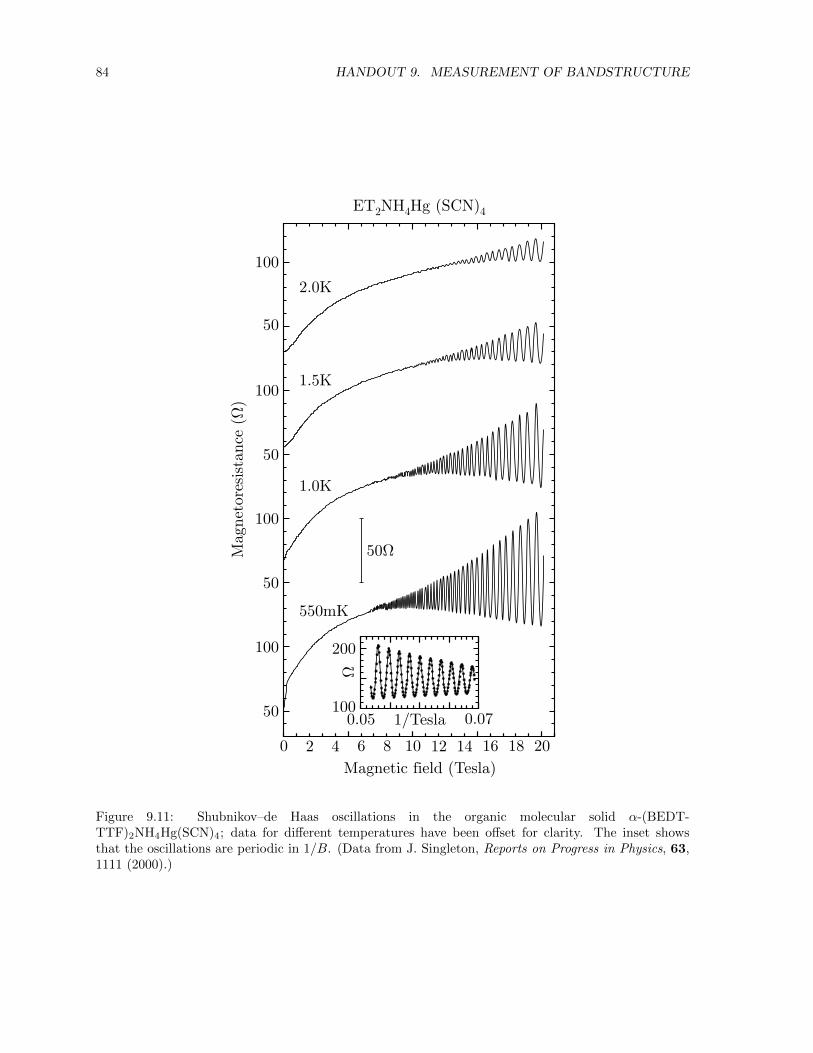
84 HANDOUT 9. MEASUREMENT OF BANDSTRUCTURE
Figure 9.11: Shubnikov–de Haas oscillations in the organic molecular solid α-(BEDT-TTF)2NH4Hg(SCN)4; data for different temperatures have been offset for clarity. The inset showsthat the oscillations are periodic in 1/B. (Data from J. Singleton, Reports on Progress in Physics, 63,1111 (2000).)
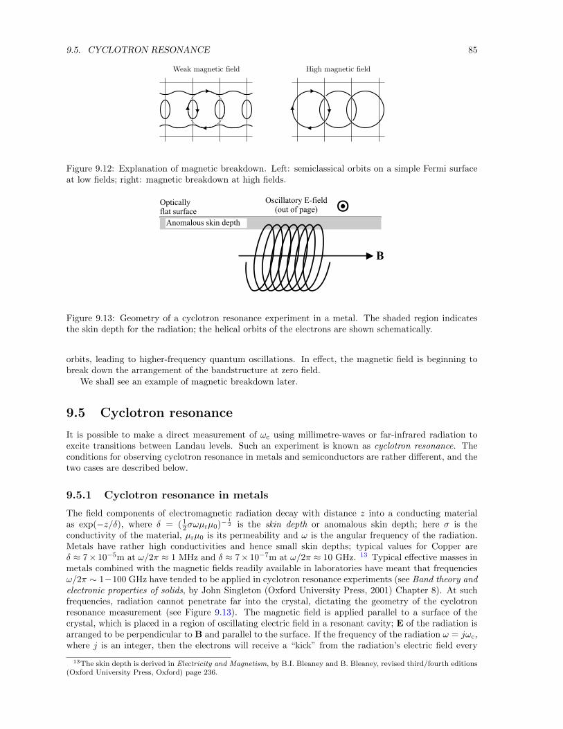
9.5. CYCLOTRON RESONANCE 85
Figure 9.12: Explanation of magnetic breakdown. Left: semiclassical orbits on a simple Fermi surfaceat low fields; right: magnetic breakdown at high fields.
Opticallyflat surface
Anomalous skin depth
B
Oscillatory E-field(out of page) o.
Figure 9.13: Geometry of a cyclotron resonance experiment in a metal. The shaded region indicatesthe skin depth for the radiation; the helical orbits of the electrons are shown schematically.
orbits, leading to higher-frequency quantum oscillations. In effect, the magnetic field is beginning tobreak down the arrangement of the bandstructure at zero field.
We shall see an example of magnetic breakdown later.
9.5 Cyclotron resonance
It is possible to make a direct measurement of ωc using millimetre-waves or far-infrared radiation toexcite transitions between Landau levels. Such an experiment is known as cyclotron resonance. Theconditions for observing cyclotron resonance in metals and semiconductors are rather different, and thetwo cases are described below.
9.5.1 Cyclotron resonance in metals
The field components of electromagnetic radiation decay with distance z into a conducting materialas exp(−z/δ), where δ = ( 1
2σωµrµ0)−12 is the skin depth or anomalous skin depth; here σ is the
conductivity of the material, µrµ0 is its permeability and ω is the angular frequency of the radiation.Metals have rather high conductivities and hence small skin depths; typical values for Copper areδ ≈ 7× 10⁻⁵m at ω/2π ≈ 1 MHz and δ ≈ 7× 10⁻⁷m at ω/2π ≈ 10 GHz. 13 Typical effective masses inmetals combined with the magnetic fields readily available in laboratories have meant that frequenciesω/2π ∼ 1−100 GHz have tended to be applied in cyclotron resonance experiments (see Band theory andelectronic properties of solids, by John Singleton (Oxford University Press, 2001) Chapter 8). At suchfrequencies, radiation cannot penetrate far into the crystal, dictating the geometry of the cyclotronresonance measurement (see Figure 9.13). The magnetic field is applied parallel to a surface of thecrystal, which is placed in a region of oscillating electric field in a resonant cavity; E of the radiation isarranged to be perpendicular to B and parallel to the surface. If the frequency of the radiation ω = jωc,where j is an integer, then the electrons will receive a “kick” from the radiation’s electric field every
13The skin depth is derived in Electricity and Magnetism, by B.I. Bleaney and B. Bleaney, revised third/fourth editions(Oxford University Press, Oxford) page 236.
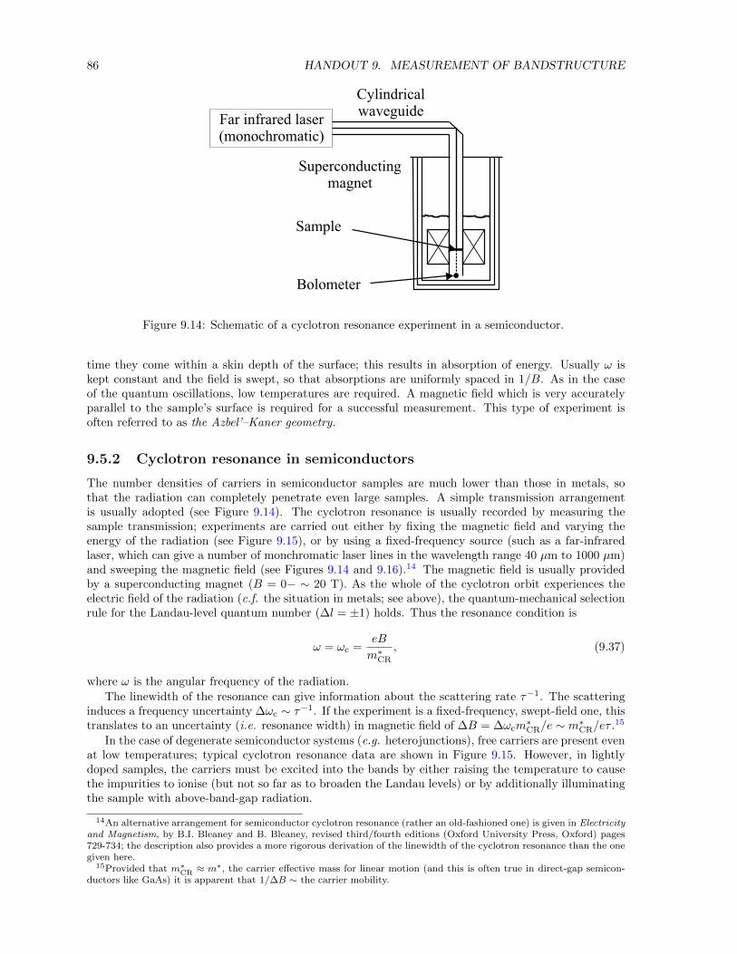
86 HANDOUT 9. MEASUREMENT OF BANDSTRUCTURE
Sample
Bolometer
Far infrared laser(monochromatic)
Cylindricalwaveguide
Superconductingmagnet
Figure 9.14: Schematic of a cyclotron resonance experiment in a semiconductor.
time they come within a skin depth of the surface; this results in absorption of energy. Usually ω iskept constant and the field is swept, so that absorptions are uniformly spaced in 1/B. As in the caseof the quantum oscillations, low temperatures are required. A magnetic field which is very accuratelyparallel to the sample’s surface is required for a successful measurement. This type of experiment isoften referred to as the Azbel’–Kaner geometry.
9.5.2 Cyclotron resonance in semiconductors
The number densities of carriers in semiconductor samples are much lower than those in metals, sothat the radiation can completely penetrate even large samples. A simple transmission arrangementis usually adopted (see Figure 9.14). The cyclotron resonance is usually recorded by measuring thesample transmission; experiments are carried out either by fixing the magnetic field and varying theenergy of the radiation (see Figure 9.15), or by using a fixed-frequency source (such as a far-infraredlaser, which can give a number of monchromatic laser lines in the wavelength range 40 µm to 1000 µm)and sweeping the magnetic field (see Figures 9.14 and 9.16).14 The magnetic field is usually providedby a superconducting magnet (B = 0− ∼ 20 T). As the whole of the cyclotron orbit experiences theelectric field of the radiation (c.f. the situation in metals; see above), the quantum-mechanical selectionrule for the Landau-level quantum number (∆l = ±1) holds. Thus the resonance condition is
ω = ωc =eB
m∗CR
, (9.37)
where ω is the angular frequency of the radiation.
The linewidth of the resonance can give information about the scattering rate τ−1. The scatteringinduces a frequency uncertainty ∆ωc ∼ τ−1. If the experiment is a fixed-frequency, swept-field one, thistranslates to an uncertainty (i.e. resonance width) in magnetic field of ∆B = ∆ωcm
∗CR/e ∼ m∗CR/eτ .15
In the case of degenerate semiconductor systems (e.g. heterojunctions), free carriers are present evenat low temperatures; typical cyclotron resonance data are shown in Figure 9.15. However, in lightlydoped samples, the carriers must be excited into the bands by either raising the temperature to causethe impurities to ionise (but not so far as to broaden the Landau levels) or by additionally illuminatingthe sample with above-band-gap radiation.
14An alternative arrangement for semiconductor cyclotron resonance (rather an old-fashioned one) is given in Electricityand Magnetism, by B.I. Bleaney and B. Bleaney, revised third/fourth editions (Oxford University Press, Oxford) pages729-734; the description also provides a more rigorous derivation of the linewidth of the cyclotron resonance than the onegiven here.
15Provided that m∗CR ≈ m∗, the carrier effective mass for linear motion (and this is often true in direct-gap semicon-
ductors like GaAs) it is apparent that 1/∆B ∼ the carrier mobility.
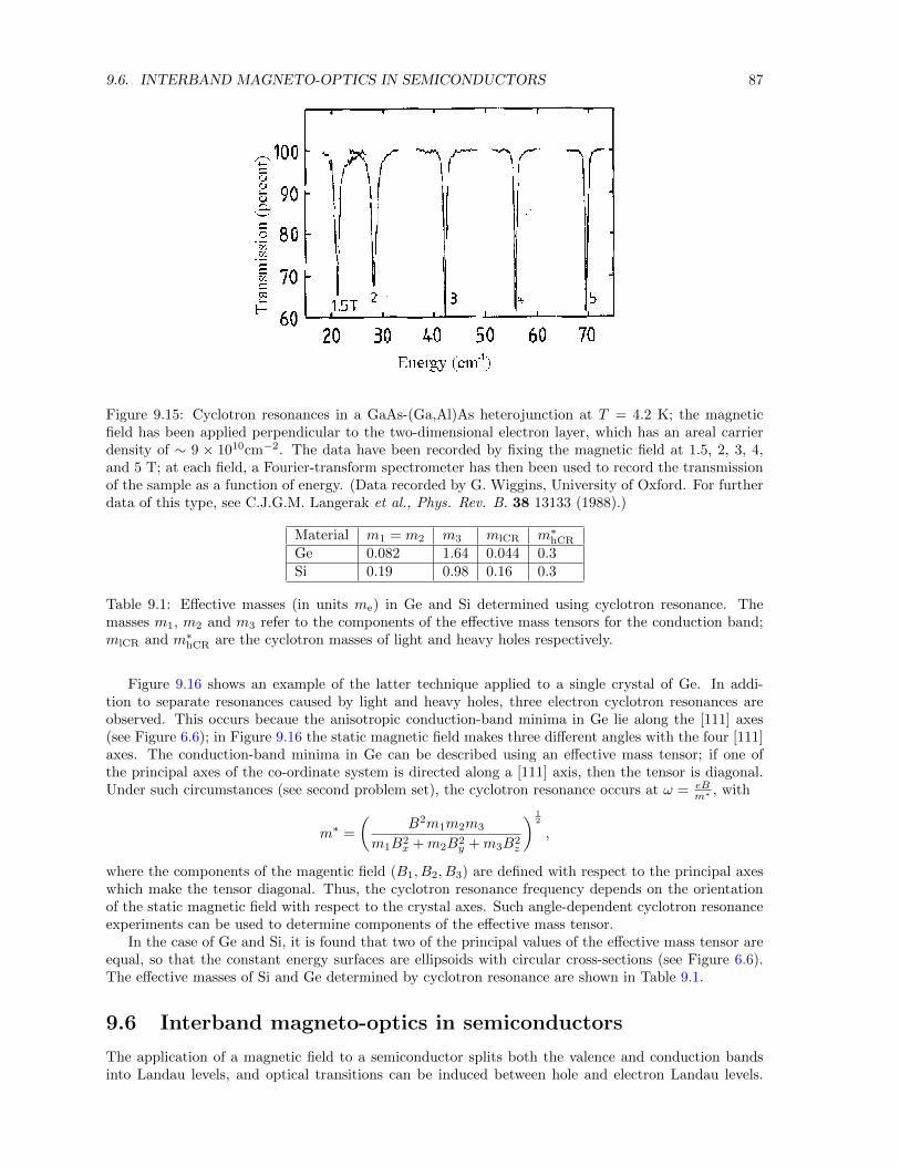
9.6. INTERBAND MAGNETO-OPTICS IN SEMICONDUCTORS 87
Figure 9.15: Cyclotron resonances in a GaAs-(Ga,Al)As heterojunction at T = 4.2 K; the magneticfield has been applied perpendicular to the two-dimensional electron layer, which has an areal carrierdensity of ∼ 9 × 1010cm−2. The data have been recorded by fixing the magnetic field at 1.5, 2, 3, 4,and 5 T; at each field, a Fourier-transform spectrometer has then been used to record the transmissionof the sample as a function of energy. (Data recorded by G. Wiggins, University of Oxford. For furtherdata of this type, see C.J.G.M. Langerak et al., Phys. Rev. B. 38 13133 (1988).)
Material m1 = m2 m3 mlCR m∗hCR
Ge 0.082 1.64 0.044 0.3Si 0.19 0.98 0.16 0.3
Table 9.1: Effective masses (in units me) in Ge and Si determined using cyclotron resonance. Themasses m1, m2 and m3 refer to the components of the effective mass tensors for the conduction band;mlCR and m∗hCR are the cyclotron masses of light and heavy holes respectively.
Figure 9.16 shows an example of the latter technique applied to a single crystal of Ge. In addi-tion to separate resonances caused by light and heavy holes, three electron cyclotron resonances areobserved. This occurs becaue the anisotropic conduction-band minima in Ge lie along the [111] axes(see Figure 6.6); in Figure 9.16 the static magnetic field makes three different angles with the four [111]axes. The conduction-band minima in Ge can be described using an effective mass tensor; if one ofthe principal axes of the co-ordinate system is directed along a [111] axis, then the tensor is diagonal.Under such circumstances (see second problem set), the cyclotron resonance occurs at ω = eB
m∗ , with
m∗ =
(B2m1m2m3
m1B2x +m2B2
y +m3B2z
) 12
,
where the components of the magentic field (B1, B2, B3) are defined with respect to the principal axeswhich make the tensor diagonal. Thus, the cyclotron resonance frequency depends on the orientationof the static magnetic field with respect to the crystal axes. Such angle-dependent cyclotron resonanceexperiments can be used to determine components of the effective mass tensor.
In the case of Ge and Si, it is found that two of the principal values of the effective mass tensor areequal, so that the constant energy surfaces are ellipsoids with circular cross-sections (see Figure 6.6).The effective masses of Si and Ge determined by cyclotron resonance are shown in Table 9.1.
9.6 Interband magneto-optics in semiconductors
The application of a magnetic field to a semiconductor splits both the valence and conduction bandsinto Landau levels, and optical transitions can be induced between hole and electron Landau levels.
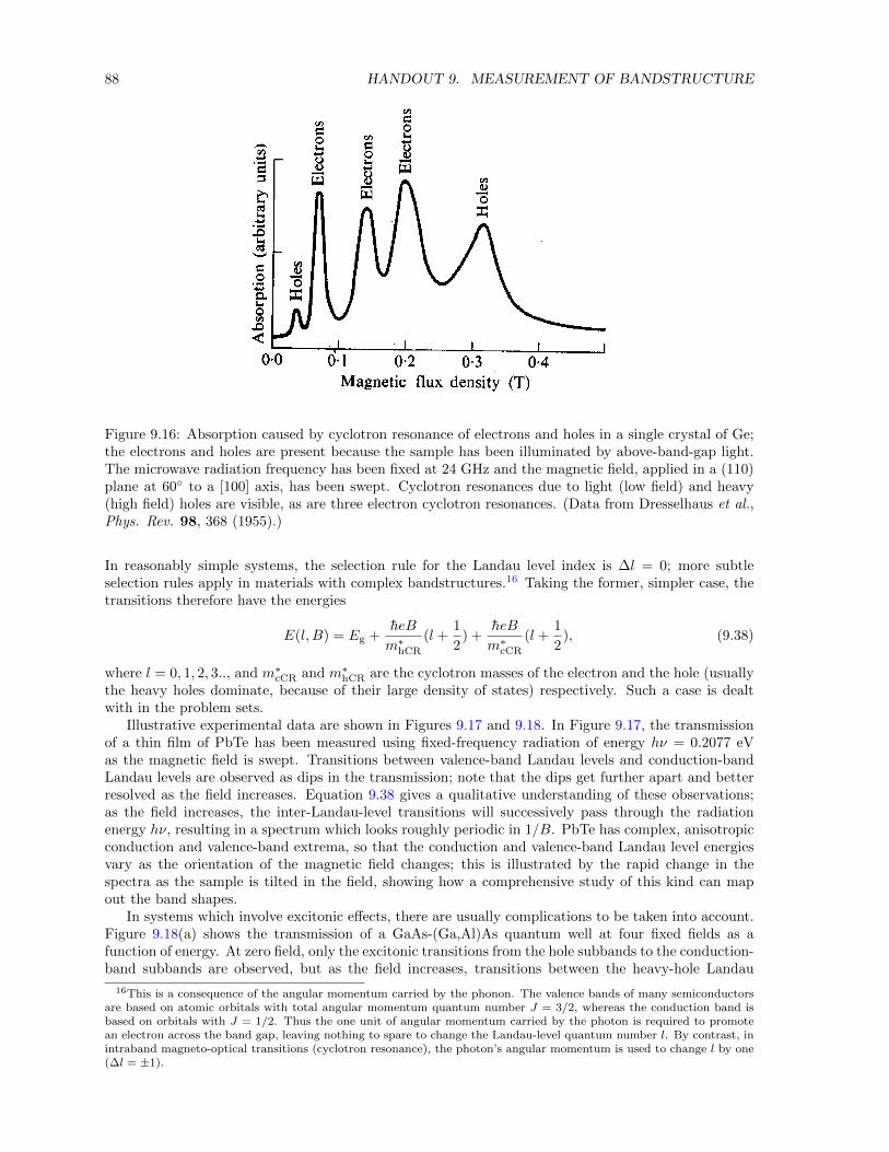
88 HANDOUT 9. MEASUREMENT OF BANDSTRUCTURE
Figure 9.16: Absorption caused by cyclotron resonance of electrons and holes in a single crystal of Ge;the electrons and holes are present because the sample has been illuminated by above-band-gap light.The microwave radiation frequency has been fixed at 24 GHz and the magnetic field, applied in a (110)plane at 60 to a [100] axis, has been swept. Cyclotron resonances due to light (low field) and heavy(high field) holes are visible, as are three electron cyclotron resonances. (Data from Dresselhaus et al.,Phys. Rev. 98, 368 (1955).)
In reasonably simple systems, the selection rule for the Landau level index is ∆l = 0; more subtleselection rules apply in materials with complex bandstructures.16 Taking the former, simpler case, thetransitions therefore have the energies
E(l, B) = Eg +heB
m∗hCR
(l +1
2) +
heB
m∗cCR
(l +1
2), (9.38)
where l = 0, 1, 2, 3.., and m∗cCR and m∗hCR are the cyclotron masses of the electron and the hole (usuallythe heavy holes dominate, because of their large density of states) respectively. Such a case is dealtwith in the problem sets.
Illustrative experimental data are shown in Figures 9.17 and 9.18. In Figure 9.17, the transmissionof a thin film of PbTe has been measured using fixed-frequency radiation of energy hν = 0.2077 eVas the magnetic field is swept. Transitions between valence-band Landau levels and conduction-bandLandau levels are observed as dips in the transmission; note that the dips get further apart and betterresolved as the field increases. Equation 9.38 gives a qualitative understanding of these observations;as the field increases, the inter-Landau-level transitions will successively pass through the radiationenergy hν, resulting in a spectrum which looks roughly periodic in 1/B. PbTe has complex, anisotropicconduction and valence-band extrema, so that the conduction and valence-band Landau level energiesvary as the orientation of the magnetic field changes; this is illustrated by the rapid change in thespectra as the sample is tilted in the field, showing how a comprehensive study of this kind can mapout the band shapes.
In systems which involve excitonic effects, there are usually complications to be taken into account.Figure 9.18(a) shows the transmission of a GaAs-(Ga,Al)As quantum well at four fixed fields as afunction of energy. At zero field, only the excitonic transitions from the hole subbands to the conduction-band subbands are observed, but as the field increases, transitions between the heavy-hole Landau
16This is a consequence of the angular momentum carried by the phonon. The valence bands of many semiconductorsare based on atomic orbitals with total angular momentum quantum number J = 3/2, whereas the conduction band isbased on orbitals with J = 1/2. Thus the one unit of angular momentum carried by the photon is required to promotean electron across the band gap, leaving nothing to spare to change the Landau-level quantum number l. By contrast, inintraband magneto-optical transitions (cyclotron resonance), the photon’s angular momentum is used to change l by one(∆l = ±1).
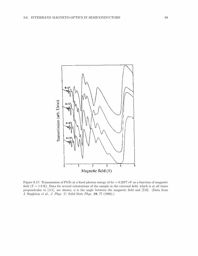
9.6. INTERBAND MAGNETO-OPTICS IN SEMICONDUCTORS 89
Figure 9.17: Transmission of PbTe at a fixed photon energy of hν = 0.2077 eV as a function of magneticfield (T = 1.9 K). Data for several orientations of the sample in the external field, which is at all timesperpendcular to [111], are shown; φ is the angle between the magnetic field and [110]. (Data fromJ. Singleton et al., J. Phys. C: Solid State Phys. 19, 77 (1986).)
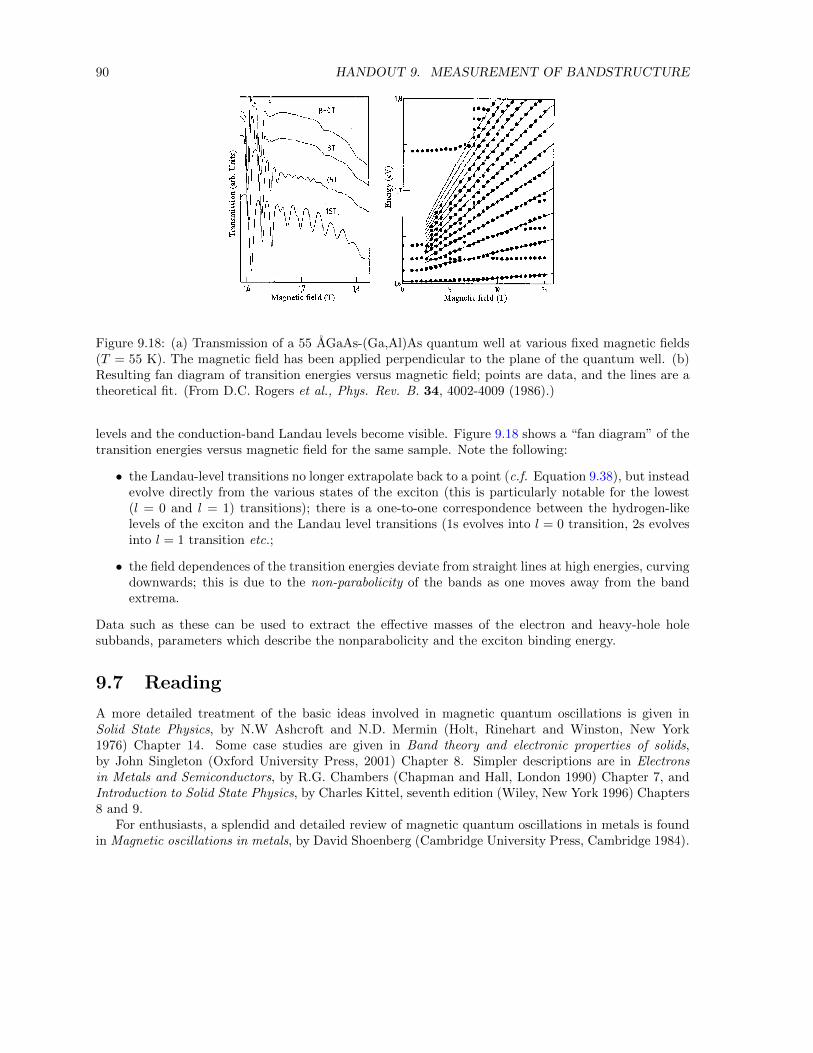
90 HANDOUT 9. MEASUREMENT OF BANDSTRUCTURE
Figure 9.18: (a) Transmission of a 55 AGaAs-(Ga,Al)As quantum well at various fixed magnetic fields(T = 55 K). The magnetic field has been applied perpendicular to the plane of the quantum well. (b)Resulting fan diagram of transition energies versus magnetic field; points are data, and the lines are atheoretical fit. (From D.C. Rogers et al., Phys. Rev. B. 34, 4002-4009 (1986).)
levels and the conduction-band Landau levels become visible. Figure 9.18 shows a “fan diagram” of thetransition energies versus magnetic field for the same sample. Note the following:
• the Landau-level transitions no longer extrapolate back to a point (c.f. Equation 9.38), but insteadevolve directly from the various states of the exciton (this is particularly notable for the lowest(l = 0 and l = 1) transitions); there is a one-to-one correspondence between the hydrogen-likelevels of the exciton and the Landau level transitions (1s evolves into l = 0 transition, 2s evolvesinto l = 1 transition etc.;
• the field dependences of the transition energies deviate from straight lines at high energies, curvingdownwards; this is due to the non-parabolicity of the bands as one moves away from the bandextrema.
Data such as these can be used to extract the effective masses of the electron and heavy-hole holesubbands, parameters which describe the nonparabolicity and the exciton binding energy.
9.7 Reading
A more detailed treatment of the basic ideas involved in magnetic quantum oscillations is given inSolid State Physics, by N.W Ashcroft and N.D. Mermin (Holt, Rinehart and Winston, New York1976) Chapter 14. Some case studies are given in Band theory and electronic properties of solids,by John Singleton (Oxford University Press, 2001) Chapter 8. Simpler descriptions are in Electronsin Metals and Semiconductors, by R.G. Chambers (Chapman and Hall, London 1990) Chapter 7, andIntroduction to Solid State Physics, by Charles Kittel, seventh edition (Wiley, New York 1996) Chapters8 and 9.
For enthusiasts, a splendid and detailed review of magnetic quantum oscillations in metals is foundin Magnetic oscillations in metals, by David Shoenberg (Cambridge University Press, Cambridge 1984).
Handout 10
Transport of heat and electricity inmetals and semiconductors
10.1 Thermal and electrical conductivity of metals
10.1.1 The “Kinetic theory” of electron transport
We now apply our knowledge of bandstructure, Fermi surfaces and electron statistics to the problem oftransport of heat and electricity by electrons. We are going to look initially at a metal with isotropicbands characterised by an effective mass m∗. This is in effect the Sommerfeld model with the additionalrefinement of an adjustable m∗ which characterises the effect of the periodic lattice potential on theelectrons; the Fermi surface will be spherical. (More complex Fermi surfaces will be mentioned later.)In Lecture 1 we used the Relaxation Time Approximation to derive the expression
σ =ne2τ
m∗(10.1)
for the electrical conductivity σ of such a metal. Here n is the number density of electrons and τ−1
is the scattering rate. In addition, we used Kinetic Theory and the Sommerfeld model to obtain theexpression
κ =1
6nπ2k2
B
T
EFv2
Fτ (10.2)
for the electronic thermal conductivity κ. Here vF is the Fermi velocity and EF is the Fermi energy.Equations 10.1 and 10.2 were combined to give the Wiedemann–Franz Ratio or Lorenz number
L ≡ κ
σT=π2
3
k2B
e2≡ L0 (10.3)
and it was found that this constant was in good agreement with many experimental data at room tem-perature. However, in many cases, experimental values of L differed markedly (by orders of magnitude!)from L0 at lower temperatures.
The problem has arisen because two scattering times τ (which are not necessarily the same) havebeen cancelled in Equation 10.3. Acknowledging this fact we rewrite Equations 10.1 and 10.2 in thefollowing form:
σ =ne2τσm∗
(10.4)
and
κ =1
6nπ2k2
B
T
EFv2
Fτκ, (10.5)
i.e. we have distinguished the two scattering times.
91
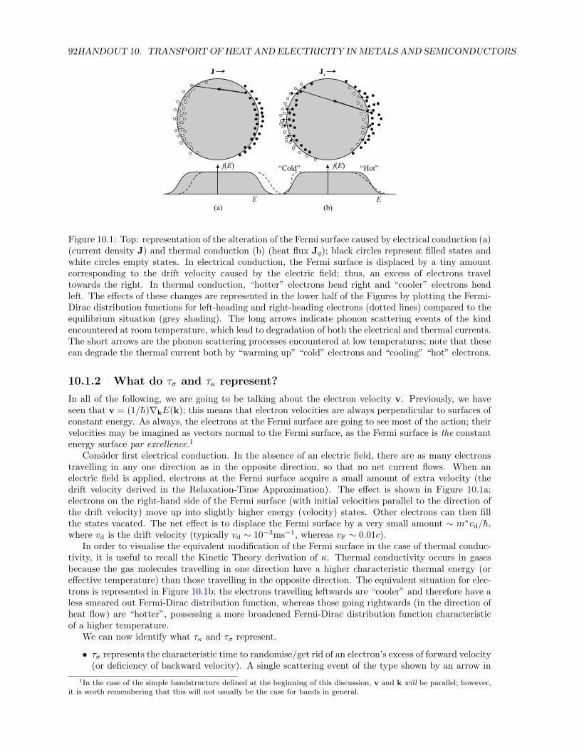
92HANDOUT 10. TRANSPORTOF HEAT AND ELECTRICITY INMETALS AND SEMICONDUCTORS
Jq
f E( )
E E
f E( )
(a) (b)
J
“Hot”“Cold”
Figure 10.1: Top: representation of the alteration of the Fermi surface caused by electrical conduction (a)(current density J) and thermal conduction (b) (heat flux Jq); black circles represent filled states andwhite circles empty states. In electrical conduction, the Fermi surface is displaced by a tiny amountcorresponding to the drift velocity caused by the electric field; thus, an excess of electrons traveltowards the right. In thermal conduction, “hotter” electrons head right and “cooler” electrons headleft. The effects of these changes are represented in the lower half of the Figures by plotting the Fermi-Dirac distribution functions for left-heading and right-heading electrons (dotted lines) compared to theequilibrium situation (grey shading). The long arrows indicate phonon scattering events of the kindencountered at room temperature, which lead to degradation of both the electrical and thermal currents.The short arrows are the phonon scattering processes encountered at low temperatures; note that thesecan degrade the thermal current both by “warming up” “cold” electrons and “cooling” “hot” electrons.
10.1.2 What do τσ and τκ represent?
In all of the following, we are going to be talking about the electron velocity v. Previously, we haveseen that v = (1/h)∇kE(k); this means that electron velocities are always perpendicular to surfaces ofconstant energy. As always, the electrons at the Fermi surface are going to see most of the action; theirvelocities may be imagined as vectors normal to the Fermi surface, as the Fermi surface is the constantenergy surface par excellence.1
Consider first electrical conduction. In the absence of an electric field, there are as many electronstravelling in any one direction as in the opposite direction, so that no net current flows. When anelectric field is applied, electrons at the Fermi surface acquire a small amount of extra velocity (thedrift velocity derived in the Relaxation-Time Approximation). The effect is shown in Figure 10.1a;electrons on the right-hand side of the Fermi surface (with initial velocities parallel to the direction ofthe drift velocity) move up into slightly higher energy (velocity) states. Other electrons can then fillthe states vacated. The net effect is to displace the Fermi surface by a very small amount ∼ m∗vd/h,where vd is the drift velocity (typically vd ∼ 10−3ms−1, whereas vF ∼ 0.01c).
In order to visualise the equivalent modification of the Fermi surface in the case of thermal conduc-tivity, it is useful to recall the Kinetic Theory derivation of κ. Thermal conductivity occurs in gasesbecause the gas molecules travelling in one direction have a higher characteristic thermal energy (oreffective temperature) than those travelling in the opposite direction. The equivalent situation for elec-trons is represented in Figure 10.1b; the electrons travelling leftwards are “cooler” and therefore have aless smeared out Fermi-Dirac distribution function, whereas those going rightwards (in the direction ofheat flow) are “hotter”, possessing a more broadened Fermi-Dirac distribution function characteristicof a higher temperature.
We can now identify what τκ and τσ represent.
• τσ represents the characteristic time to randomise/get rid of an electron’s excess of forward velocity(or deficiency of backward velocity). A single scattering event of the type shown by an arrow in
1In the case of the simple bandstructure defined at the beginning of this discussion, v and k will be parallel; however,it is worth remembering that this will not usually be the case for bands in general.
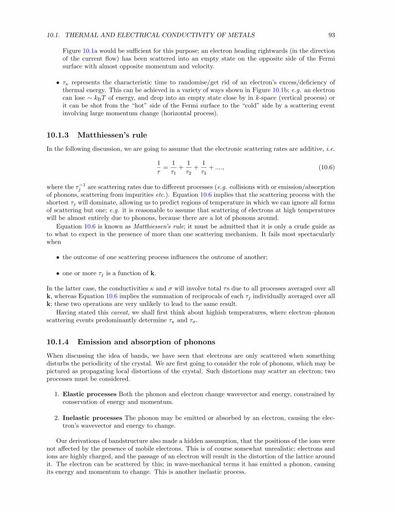
10.1. THERMAL AND ELECTRICAL CONDUCTIVITY OF METALS 93
Figure 10.1a would be sufficient for this purpose; an electron heading rightwards (in the directionof the current flow) has been scattered into an empty state on the opposite side of the Fermisurface with almost opposite momentum and velocity.
• τκ represents the characteristic time to randomise/get rid of an electron’s excess/deficiency ofthermal energy. This can be achieved in a variety of ways shown in Figure 10.1b; e.g. an electroncan lose ∼ kBT of energy, and drop into an empty state close by in k-space (vertical process) orit can be shot from the “hot” side of the Fermi surface to the “cold” side by a scattering eventinvolving large momentum change (horizontal process).
10.1.3 Matthiessen’s rule
In the following discussion, we are going to assume that the electronic scattering rates are additive, i.e.
1
τ=
1
τ1+
1
τ2+
1
τ3+ ...., (10.6)
where the τ−1j are scattering rates due to different processes (e.g. collisions with or emission/absorption
of phonons, scattering from impurities etc.). Equation 10.6 implies that the scattering process with theshortest τj will dominate, allowing us to predict regions of temperature in which we can ignore all formsof scattering but one; e.g. it is reasonable to assume that scattering of electrons at high temperatureswill be almost entirely due to phonons, because there are a lot of phonons around.
Equation 10.6 is known as Matthiessen’s rule; it must be admitted that it is only a crude guide asto what to expect in the presence of more than one scattering mechanism. It fails most spectacularlywhen
• the outcome of one scattering process influences the outcome of another;
• one or more τj is a function of k.
In the latter case, the conductivities κ and σ will involve total τs due to all processes averaged over allk, whereas Equation 10.6 implies the summation of reciprocals of each τj individually averaged over allk; these two operations are very unlikely to lead to the same result.
Having stated this caveat, we shall first think about highish temperatures, where electron–phononscattering events predominantly determine τκ and τσ.
10.1.4 Emission and absorption of phonons
When discussing the idea of bands, we have seen that electrons are only scattered when somethingdisturbs the periodicity of the crystal. We are first going to consider the role of phonons, which may bepictured as propagating local distortions of the crystal. Such distortions may scatter an electron; twoprocesses must be considered.
1. Elastic processes Both the phonon and electron change wavevector and energy, constrained byconservation of energy and momentum.
2. Inelastic processes The phonon may be emitted or absorbed by an electron, causing the elec-tron’s wavevector and energy to change.
Our derivations of bandstructure also made a hidden assumption, that the positions of the ions werenot affected by the presence of mobile electrons. This is of course somewhat unrealistic; electrons andions are highly charged, and the passage of an electron will result in the distortion of the lattice aroundit. The electron can be scattered by this; in wave-mechanical terms it has emitted a phonon, causingits energy and momentum to change. This is another inelastic process.

94HANDOUT 10. TRANSPORTOF HEAT AND ELECTRICITY INMETALS AND SEMICONDUCTORS
q
qk k
1 F
k1
electron
k k2 F~-
k k2 F~-
~-
Fermi surface
µ
Figure 10.2: Geometry of electron-phonon scattering events at T ∼ θD (left) and T θD (right). Ineach case k1 and k2 are the initial and final electron wavevectors (both of magnitude ≈ kF) and q isthe phonon wavevector.
10.1.5 What is the characteristic energy of the phonons involved?
Phonons behave as massless bosons, that is to say they can be created and destroyed in a similar wayto photons.2 Phonons therefore have a “black-body” type of energy distribution, with a peak at anenergy ∼ kBT , i.e. the characteristic phonon energy at a temperature T is hω ∼ kBT . We thereforeexpect that when an electron scatters from or absorbs a phonon, that phonon will typically have anenergy ∼ kBT .
But what about the emission of phonons? The form of the Fermi–Dirac distribution function forthe electrons means that the only empty states below the Fermi energy have energies EF − (∼ kBT ).Similarly, the energy of the most energetic electrons will be roughly EF + (∼ kBT ). Therefore, anelectron can only emit a phonon with energy ∼ kBT , i.e. even though the electron distorts the latticeat low temperatures, it cannot emit energetic phonons because there are no accessible final states forsuch a process!
The probability of emitting a phonon of energy ∼ kBT will have a very similar temperature depen-dence to the probability of absorbing such a phonon. This is easy to see when one considers that thelatter depends on the number of phonons around with such an energy (i.e. on the phonon density ofstates at an energy hω ∼ kBT ) whereas the former depends on the density of available final phononstates (i.e. the phonon density of states at an energy hω ∼ kBT ).
Therefore, in all that follows, I am just going to talk about elastic phonon scattering processes andinelastic phonon scattering processes where the latter means either emission or absorption of phonons;i.e. I shall assume that the probability of all processes involving phonons will follow a similar temper-ature dependence.
10.1.6 Electron–phonon scattering at room temperature
The Debye temperatures θD of most metals are less than or of the order of room temperature. Now θD isroughly the energy of the most energetic phonons in the metal, so that phonons with energy hω ∼ kBTwill have wavevectors q ≈ (half the width of the Brillouin zone) ∼ kF, where kF is the Fermi wavevector.Thus one phonon scattering event (inelastic or elastic) will scatter the electron to the opposite side ofthe Fermi surface (see Figure 10.2). Thus τ−1
σ ≈ τ−1κ ∝ (number of phonons with hω ∼ kBT ) ∝ T .
10.1.7 Electron-phonon scattering at T θD
In this case, phonons with energy hω ∼ kBT will have energies kBθD and therefore q (Brillouinzone size), i.e. q kF. Thus, one inelastic phonon scattering event will be able to change the electron’senergy by ∼ kBT ; hence τ−1
κ ∝ (number of phonons with hω ∼ kBT ) ∝ T 3.3 However, one phononscattering event (elastic or inelastic) will be unable to knock the electron to the other side of the Fermi
2See Statistical Mechanics books such as e.g. Statistical Physics, by Tony Guenault (Routledge, London 1988) page124 .
3The T 3 power is well known from the Debye heat capacity derivation.
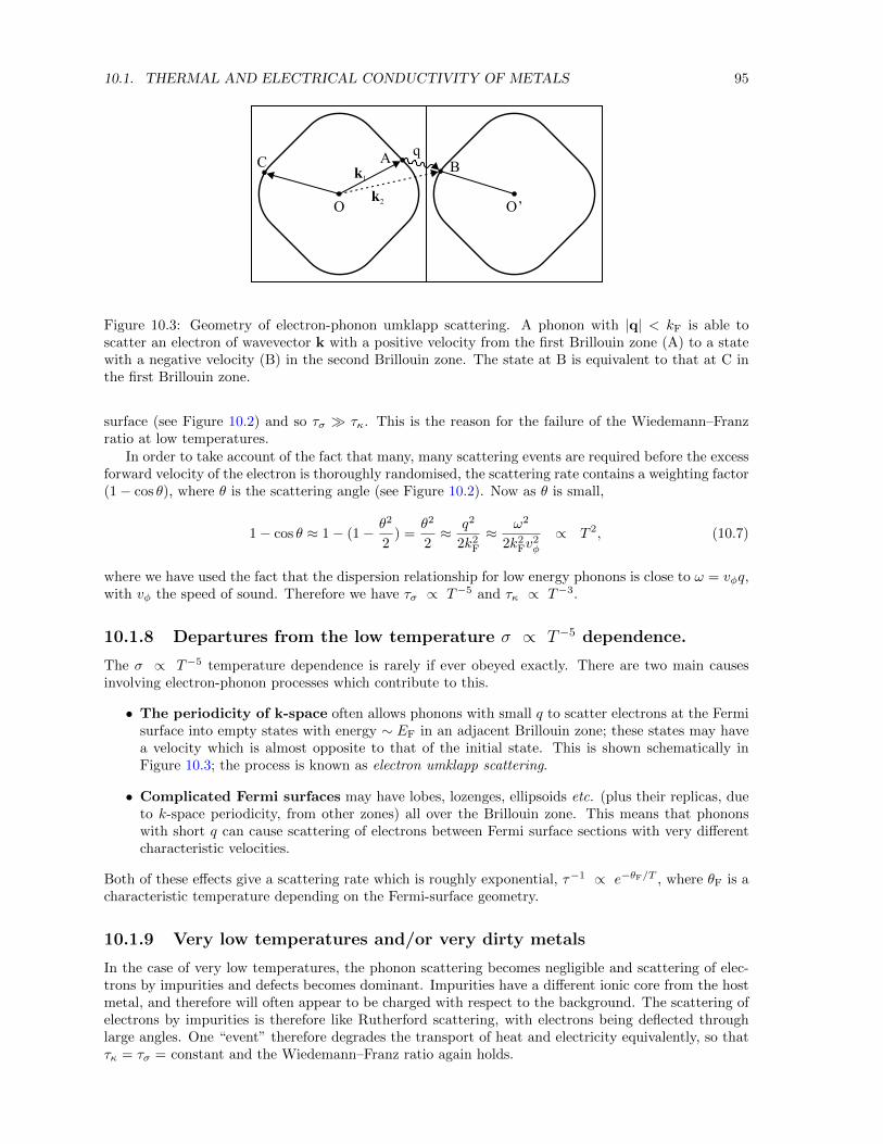
10.1. THERMAL AND ELECTRICAL CONDUCTIVITY OF METALS 95
qC A
k1
k2O O’
B
Figure 10.3: Geometry of electron-phonon umklapp scattering. A phonon with |q| < kF is able toscatter an electron of wavevector k with a positive velocity from the first Brillouin zone (A) to a statewith a negative velocity (B) in the second Brillouin zone. The state at B is equivalent to that at C inthe first Brillouin zone.
surface (see Figure 10.2) and so τσ τκ. This is the reason for the failure of the Wiedemann–Franzratio at low temperatures.
In order to take account of the fact that many, many scattering events are required before the excessforward velocity of the electron is thoroughly randomised, the scattering rate contains a weighting factor(1− cos θ), where θ is the scattering angle (see Figure 10.2). Now as θ is small,
1− cos θ ≈ 1− (1− θ2
2) =
θ2
2≈ q2
2k2F
≈ ω2
2k2Fv
2φ
∝ T 2, (10.7)
where we have used the fact that the dispersion relationship for low energy phonons is close to ω = vφq,with vφ the speed of sound. Therefore we have τσ ∝ T−5 and τκ ∝ T−3.
10.1.8 Departures from the low temperature σ ∝ T−5 dependence.
The σ ∝ T−5 temperature dependence is rarely if ever obeyed exactly. There are two main causesinvolving electron-phonon processes which contribute to this.
• The periodicity of k-space often allows phonons with small q to scatter electrons at the Fermisurface into empty states with energy ∼ EF in an adjacent Brillouin zone; these states may havea velocity which is almost opposite to that of the initial state. This is shown schematically inFigure 10.3; the process is known as electron umklapp scattering.
• Complicated Fermi surfaces may have lobes, lozenges, ellipsoids etc. (plus their replicas, dueto k-space periodicity, from other zones) all over the Brillouin zone. This means that phononswith short q can cause scattering of electrons between Fermi surface sections with very differentcharacteristic velocities.
Both of these effects give a scattering rate which is roughly exponential, τ−1 ∝ e−θF/T , where θF is acharacteristic temperature depending on the Fermi-surface geometry.
10.1.9 Very low temperatures and/or very dirty metals
In the case of very low temperatures, the phonon scattering becomes negligible and scattering of elec-trons by impurities and defects becomes dominant. Impurities have a different ionic core from the hostmetal, and therefore will often appear to be charged with respect to the background. The scattering ofelectrons by impurities is therefore like Rutherford scattering, with electrons being deflected throughlarge angles. One “event” therefore degrades the transport of heat and electricity equivalently, so thatτκ = τσ = constant and the Wiedemann–Franz ratio again holds.

96HANDOUT 10. TRANSPORTOF HEAT AND ELECTRICITY INMETALS AND SEMICONDUCTORS
Temperature Scattering κ W-F ratio(scatterer) times σVery low τκ ≈ τσ κ ∝ T , L0
(impurities) ∼ const σ ∼ constT ∼ θD/10 τκ ∝ T−3, κ ∝ T−2, < L0
(phonons) τσ ∝ T−5 → e−θF/T σ ∝ T−5 → e−θF/T
T >∼ θD τκ ≈ τσ κ =const, L0
(phonons) ∝ T−1 σ ∝ T−1
Table 10.1: Summary of the temperature dependences of scattering times and electrical and thermalconductivities.
10.1.10 Summary
A summary of the temperature dependences of scattering times and electrical and thermal conductivitiesis given in Table 1. Typical electrical resistivity and thermal conductivity data are shown in Figures 10.4and 10.5. Note that for reasonably pure metals with reasonably simple bandstructures (e.g. alkali andnoble metals), electrical resistivity data are all of a similar form, and when normalised to the valueat T = θR lie roughly on the same curve when plotted against T/θR (see Figure 10.4); here θR is acharacteristic temperature similar (but not identical) to θD.
10.1.11 Electron–electron scattering
In metals with simple Fermi surfaces, electron–electron scattering is relatively unimportant. Initial andfinal states for both electrons must have energies close to EF and wavevectors close in magnitude tokF; in addition, energy and momentum must be conserved. The combination of these two requirementsmakes electron-electron scattering quite unlikely (and actually completely forbidden at T = 0).
However, electron-electron scattering becomes more important when
• the Fermi surface is complicated, so that there the conservation of energy and momentum becomeseasy for a wider variety of possible scattering processes and/or
• the density of states at the Fermi energy is very large (because the effective mass is large), bumpingup the number of initial and final states (e.g. transition metals, heavy fermion compounds).
Reasonably simple arguments4 show that electron-electron scattering leads to τ−1 ∝ T 2.Some typical data for transition metals are shown in Figure 10.6. At low temperatures, the resis-
tivities tend towards the T 2 dependence expected for electron-electron scattering.
10.2 Electrical conductivity of semiconductors
10.2.1 Temperature dependence of the carrier densities
Over wide ranges of temperature, the dominant contribution to the temperature dependence of the elec-trical conductivity is the rapidly varying number of free carriers. Recalling the results of Section 6.3.4,in order to find n and p when impurities are present we use the law of Mass Action (Equation 6.12)
np = T 3We− EgkBT
combined with the conservation law (Equation 6.17)
n− p = ND −NA,
where ND is the density of donors and NA is the density of acceptors (both are assumed to only provideone carrier each).
4See e.g. Solid State Physics, by N.W Ashcroft and N.D. Mermin (Holt, Rinehart and Winston, New York 1976) page347.
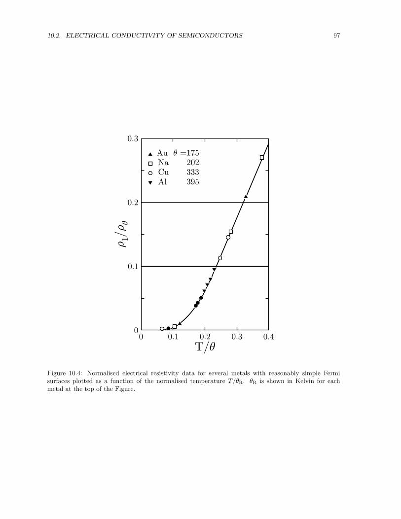
10.2. ELECTRICAL CONDUCTIVITY OF SEMICONDUCTORS 97
0.3
0.2
0.1
00 0.1 0.2 0.3 0.4
T/µ
Au =175µ
NaCuAl
202333395
½½
1/
µ
Figure 10.4: Normalised electrical resistivity data for several metals with reasonably simple Fermisurfaces plotted as a function of the normalised temperature T/θR. θR is shown in Kelvin for eachmetal at the top of the Figure.
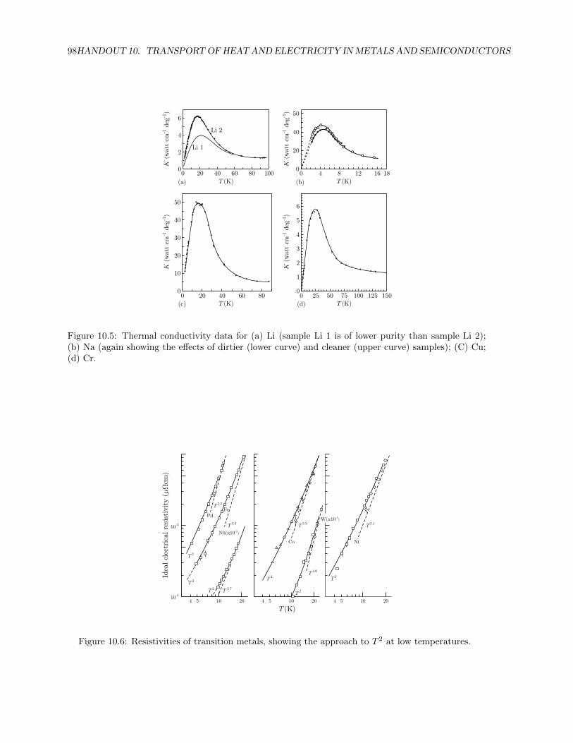
98HANDOUT 10. TRANSPORTOF HEAT AND ELECTRICITY INMETALS AND SEMICONDUCTORS
1000 20 40 60 800
2
4
6
Li 2
Li 1
K(w
att
cm
deg
)-1
-1
K(w
att
cm
deg
)-1
-1
K(w
att
cmdeg
)-1
-1
K(w
att
cmdeg
)-1
-1
(a)
(c)
50
40
30
20
10
00
20 40 60 80
(d)
40
50
20
00 4 8 12 16 18
(b)
0
6
5
4
3
2
1
025 50 75 100 125 150
T (K)
T (K)
T (K)
T (K)
Figure 10.5: Thermal conductivity data for (a) Li (sample Li 1 is of lower purity than sample Li 2);(b) Na (again showing the effects of dirtier (lower curve) and cleaner (upper curve) samples); (C) Cu;(d) Cr.
Figure 10.6: Resistivities of transition metals, showing the approach to T 2 at low temperatures.
10.3. READING 99
The electrical conductivity of a semiconductor consists of a sum of contributions from all carriertypes. The simple model of Section 6.3.4, which is a reasonable approximation for many semiconduc-tors, has just two types, electrons and heavy holes. Therefore, the conductivity will contain just twocontributions, i.e.
σ = neµc + peµhh, (10.8)
where µc and µhh are the electron and hole mobilities respectively. The mobilities are defined as the driftvelocity of the carrier per unit electric field; the Relaxation-Time Approximation (see the derivation ofEquation 1.6) can be used to give
µc =eτcm∗c
(10.9)
andµhh =
eτhh
m∗hh
, (10.10)
where τ−1c and τ−1
hh are the scattering rates for the electrons in the conduction band and the heavy holesin the valence band respectively.
The temperature dependence of the electrical conductivity is therefore determined by convolutionsof the temperature dependences of n and τc and p and τhh.
When n ≥ p (n-type or intrinsic semiconductors) the holes can be completely ignored in most cases;this is because in the majority of semiconductors, the electrons have a much smaller effective mass thanthe holes, resulting in a smaller density of states and hence a longer τ . Therefore the electron mobilityis often much, much greater than that of the holes.
10.2.2 The temperature dependence of the mobility
There are two important sources of scattering.
1. Impurities (T θD). Charged impurity scattering is rather like Rutherford scattering; hencethe scattering cross-section varies as E−2. In the nondegenerate case, E ∼ kBT , so that thecross-section is proportional to T−2; hence the mean-free path is proportional to T 2. The carrierspeed is proportional to E
12 , i.e. T
12 . Therefore
τ ∝ T−12
T−2= T
32 . (10.11)
Note that this contrasts greatly with the situation in metals (τ ∼ constant for impurity scattering),where all of the action goes on at or close to the Fermi surface; the carriers which scatter from theimpurities in metals (see Section 10.1.9) have virtually constant (i.e. temperature-independent)energies. In non-degenerate semiconductors, the free carriers have a quasi-Boltzmann-like energydistribution, so that the average energy of the carriers varies with temperature.
2. Phonons (T ∼ θD). The number of phonons at such temperatures will be proportional to T(see Section 10.1.6), leading to a mean-free-path proportional to T−1. As before, the speed is
proportional to T12 . Therefore
τ ∝ T−1
T12
= T−32 . (10.12)
10.3 Reading
There are a large number of similar treatments of this topic e.g. (in increasing order of complexity)Electricity and Magnetism, by B.I. Bleaney and B. Bleaney, revised third/fourth editions (OxfordUniversity Press, Oxford) Chapters 11, 17; Solid State Physics, by G. Burns (Academic Press, Boston,1995) Sections 9.1-9.14; Introduction to Solid State Physics, by Charles Kittel, seventh edition (Wiley,New York 1996) Chapters 6 and 7; Solid State Physics, by N.W Ashcroft and N.D. Mermin (Holt,Rinehart and Winston, New York 1976) Chapters 1-3, 29. See also sections 4.23-4.27 of Low temperaturesolid state physics, by H.M. Rosenberg (OUP 1963).

100HANDOUT 10. TRANSPORTOF HEAT AND ELECTRICITY INMETALS AND SEMICONDUCTORS
Handout 11
Magnetoresistance inthree-dimensional systems
11.1 Introduction
Magnetoresistance is a general term for the changes in the components of the resistivity and conductivitytensors of materials caused by the application of magnetic field. We are going to treat the magnetore-sistance of metals in a quite general and simple manner. First, however, the Hall effect in a system withmore than one type of carrier will be described, as it helps to illuminate the more general discussion ofmetals that will follow, and gives a clue as to the origins of magnetoresistance.
11.2 Hall effect with more than one type of carrier
11.2.1 General considerations
We consider the Hall effect with two or more carrier types present (e.g. electrons and holes). Thegeometry of a Hall effect measurement is shown in Figure 11.1; the magnetic field B is applied parallelto the z direction (i.e. B = (0, 0, B)), whilst the current I is driven through the sample in the xdirection. The electric field E is assumed to be E = (Ex, Ey, 0); we assume that any effect is going tooccur in the plane perpendicular to B because of the nature of the Lorentz force (see Equation 11.1below). Voltage measuring contacts are provided on the sample so that Ex and Ey can be deduced (seeFigure 11.1).
We assume that the drift velocity v of each species of carrier can be treated using the RelaxationTime Approximation, i.e.
m∗dv
dt+
v
τ = qE + qv ×B, (11.1)
where q is the charge of the carrier, m∗ is its effective mass (assumed isotropic and energy-independent)and τ−1 is its relaxation (scattering) rate. Note that all changes in v occur in the plane perpendicularto B; therefore it is sufficient to split Equation 11.1 into x and y components to give
m∗dvxdt
+vxτ = qEx + qvyB (11.2)
and
m∗dvydt
+vyτ = qEy − qvxB. (11.3)
The Hall effect represents a steady state of the system, i.e. dvx/dt = dvy/dt = 0. SubstitutingEquation 11.2 into Equation 11.3 with dvx/dt = dvy/dt = 0 gives
m∗vyτ
= qEy −qBτ
m∗qEx + qvyB, (11.4)
101
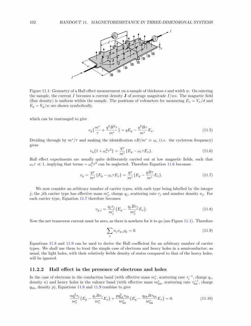
102 HANDOUT 11. MAGNETORESISTANCE IN THREE-DIMENSIONAL SYSTEMS
Figure 11.1: Geometry of a Hall effect measurement on a sample of thickness s and width w. On enteringthe sample, the current I becomes a current density J of average magnitude I/ws. The magnetic field(flux density) is uniform within the sample. The positions of voltmeters for measuring Ex = Vx/d andEy = Vy/w are shown symbolically.
which can be rearranged to give
vym∗
τ+q2B2τ
m∗ = qEy −
q2Bτ
m∗Ex. (11.5)
Dividing through by m∗/τ and making the identification eB/m∗ ≡ ωc (i.e. the cyclotron frequency)gives
vy1 + ω2cτ
2 =qτ
m∗Ey − ωcτEx. (11.6)
Hall effect experiments are usually quite deliberately carried out at low magnetic fields, such thatωcτ 1, implying that terms ∼ ω2
cτ2 can be neglected. Therefore Equation 11.6 becomes
vy =qτ
m∗Ey − ωcτEx =
qτ
m∗Ey −
qBτ
m∗Ex. (11.7)
We now consider an arbitrary number of carrier types, with each type being labelled by the integerj; the jth carrier type has effective mass m∗j , charge qj , scattering rate τj and number density nj . Foreach carrier type, Equation 11.7 therefore becomes
vy,j =qjτjm∗jEy −
qjBτjm∗j
Ex. (11.8)
Now the net transverse current must be zero, as there is nowhere for it to go (see Figure 11.1). Therefore∑j
njvy,jqj = 0. (11.9)
Equations 11.8 and 11.9 can be used to derive the Hall coefficient for an arbitrary number of carriertypes. We shall use them to treat the simple case of electrons and heavy holes in a semiconductor; asusual, the light holes, with their relatively feeble density of states compared to that of the heavy holes,will be ignored.
11.2.2 Hall effect in the presence of electrons and holes
In the case of electrons in the conduction band (with effective mass m∗c , scattering rate τ−1c , charge qc,
density n) and heavy holes in the valence band (with effective mass m∗hh, scattering rate τ−1hh , charge
qhh, density p), Equations 11.8 and 11.9 combine to give
nq2cτcm∗cEy −
qcBτcm∗c
Ex+pq2
hhτhh
m∗hh
Ey −qhhBτhh
m∗hh
Ex = 0. (11.10)
11.3. MAGNETORESISTANCE IN METALS 103
Equation 11.10 can be rearranged to give
Eynµc + pµhh = Expµ2hh − nµ2
cB, (11.11)
where µhh = |qhhτhh/m∗hh| is the heavy hole mobility and where µc = |qcτc/m
∗c | is the electron mobility,
and I have substituted qhh ≡ +e and qc ≡ −e. Now
Ex =Jxσ
=Jx
|e|(nµc + pµhh), (11.12)
where Jx is the current density in the x direction. Combining Equations 11.11 and 11.12 gives
RH ≡EyJxB
=1
|e|(pµ2
hh − nµ2c)
(nµc + pµhh)2. (11.13)
This treatment is explored in more depth in the Problems.1
11.2.3 A clue about the origins of magnetoresistance
Equations 11.9 and 11.10 show that, although no net current flows in the y direction, the currentscarried in the y direction by a particular type of carrier may (i.e. probably will) be non-zero. Carriersflowing in the y direction will experience a Lorentz force caused by B in the negative x direction (youcan satisfy yourself that this will always be the case). This backflow of carriers will act to change theapparent resistivity Ex/Jx, i.e. cause magnetoresistance.2
In the following Section we shall explore this idea more formally and in a very general manner. Weshall see that the presence of more than one “carrier type” (and here the term is used very imprecisely)is necessary for magnetoresistance to be observed.
In order to treat all of the different contributions to the conductivity and resistivity in a sanitaryfashion, we shall introduce the idea of conductivity and resistivity tensors.
11.3 Magnetoresistance in metals
11.3.1 The absence of magnetoresistance in the Sommerfeld model of metals
We consider first of all a metal with a simple spherical Fermi surface and isotropic, energy-independenteffective mass. As in Section 11.2.1, the magnetic field B will be parallel to z (see Figure 11.1), and weshall use the same symbols (effective mass m∗, scattering rate τ−1 and electronic charge −e). ApplyingEquation 11.1, we have
m∗dv
dt+
v
τ = −eE− ev ×B. (11.14)
Two things may be deduced from this equation.
• The motion of the electrons in the direction parallel to B is unaffected. Therefore there will beno longitudinal magnetoresistance; in this context, the longitudinal resistivity is measured in thedirection parallel to the field B (i.e. both the applied current density and the measured electricfield are parallel to B).
• There may well be transverse magnetoresistance. Here transverse resistivity means that measuredin the direction perpendicular to the field B (i.e. both the applied current density and themeasured electric field are in the plane perpendicular to B).
1Some excellent illustrative data are shown in Figure 4.3 of Semiconductor Physics, by K. Seeger (Springer, Berlin1991).
2Those who are unconvinced by this hand-waving argument should go back to Equation 11.6 and repeat the abovederivation for ωcτ 1. They will find that ((p/µhh) + (n/µc))Ey = (p − n)ExB (i.e the Hall field is zero if n = p).Putting n = p yields Jx = ((p/µhh)+(n/µc))eEx/B2, i.e. ρ ∝ B2. This is the reason for the very large magnetoresistancein compensated semimetals (equal number of holes and electrons at Fermi surface) such as Bi.
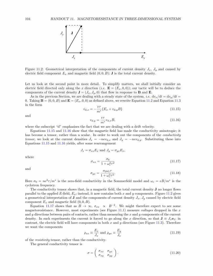
104 HANDOUT 11. MAGNETORESISTANCE IN THREE-DIMENSIONAL SYSTEMS
Jx Ex
Jy J
Figure 11.2: Geometrical interpretation of the components of current density Jx, Jy and caused byelectric field component Ex and magnetic field (0, 0, B); J is the total current density.
Let us look at the second point in more detail. To simplify matters, we shall initially consider anelectric field directed only along the x direction (i.e. E = (Ex, 0, 0)); our tactic will be to deduce thecomponents of the current density J = (Jx, Jy, 0) that flow in response to B and E.
As in the previous Section, we are dealing with a steady state of the system, i.e. dvx/dt = dvy/dt =0. Taking B = (0, 0, B) and E = (Ex, 0, 0) as defined above, we rewrite Equation 11.2 and Equation 11.3in the form
vd,x = − eτm∗Ex + vd,yB (11.15)
andvd,y =
eτ
m∗vd,xB, (11.16)
where the subscript “d” emphasises the fact that we are dealing with a drift velocity.Equations 11.15 and 11.16 show that the magnetic field has made the conductivity anisotropic; it
has become a tensor, rather than a scalar. In order to work out the components of the conductivitytensor, we look at the current densities Jx = −nevd,x and Jy = −nevd,y. Substituting these intoEquations 11.15 and 11.16 yields, after some rearrangement
Jx = σxxEx and Jy = σyxEx,
whereσxx =
σ0
1 + ω2cτ
2(11.17)
andσyx =
σ0ωcτ
1 + ω2cτ
2. (11.18)
Here σ0 = ne2τ/m∗ is the zero-field conductivity in the Sommerfeld model and ωc = eB/m∗ is thecyclotron frequency.
The conductivity tensor shows that, in a magnetic field, the total current density J no longer flowsparallel to the applied E-field, Ex; instead, it now contains both x and y components. Figure 11.2 givesa geometrical interpretation of J and the components of current density Jx, Jy caused by electric fieldcomponent Ex and magnetic field (0, 0, B).
Equation 11.17 shows that as B → ∞, σxx ∝ B−2. We might therefore expect to see somemagnetoresistance. However, most experiments (see Figure 11.1) measure voltages dropped in the xand y directions between pairs of contacts, rather than measuring the x and y components of the currentdensity. In such experiments the current is forced to go along the x direction, so that J ≡ Jxe1; incontrast, the electric field will have components in both x and y directions (see Figure 11.3). Thereforewe want the components
ρxx ≡ExJx
and ρyx ≡EyJx
(11.19)
of the resistivity tensor, rather than the conductivity.The general conductivity tensor is
σ =
(σxx σyxσxy σyy
). (11.20)
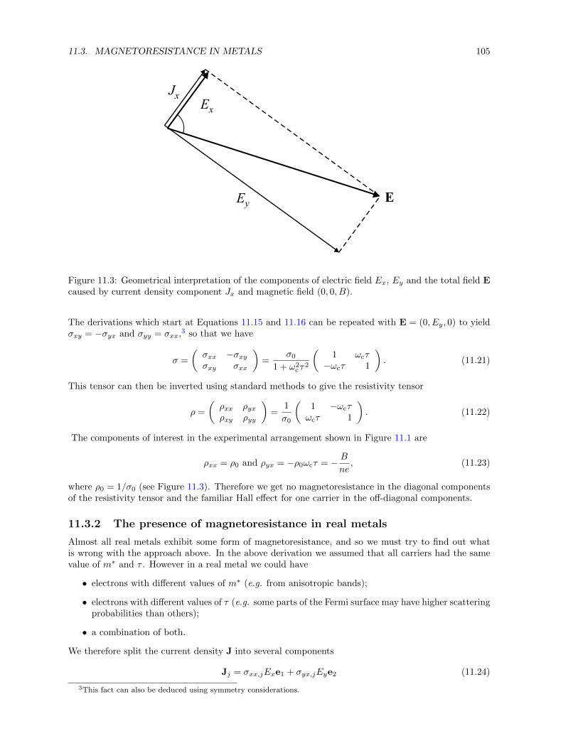
11.3. MAGNETORESISTANCE IN METALS 105
JxEx
EyE
Figure 11.3: Geometrical interpretation of the components of electric field Ex, Ey and the total field Ecaused by current density component Jx and magnetic field (0, 0, B).
The derivations which start at Equations 11.15 and 11.16 can be repeated with E = (0, Ey, 0) to yieldσxy = −σyx and σyy = σxx,3 so that we have
σ =
(σxx −σxyσxy σxx
)=
σ0
1 + ω2cτ
2
(1 ωcτ−ωcτ 1
). (11.21)
This tensor can then be inverted using standard methods to give the resistivity tensor
ρ =
(ρxx ρyxρxy ρyy
)=
1
σ0
(1 −ωcτωcτ 1
). (11.22)
The components of interest in the experimental arrangement shown in Figure 11.1 are
ρxx = ρ0 and ρyx = −ρ0ωcτ = − Bne, (11.23)
where ρ0 = 1/σ0 (see Figure 11.3). Therefore we get no magnetoresistance in the diagonal componentsof the resistivity tensor and the familiar Hall effect for one carrier in the off-diagonal components.
11.3.2 The presence of magnetoresistance in real metals
Almost all real metals exhibit some form of magnetoresistance, and so we must try to find out whatis wrong with the approach above. In the above derivation we assumed that all carriers had the samevalue of m∗ and τ . However in a real metal we could have
• electrons with different values of m∗ (e.g. from anisotropic bands);
• electrons with different values of τ (e.g. some parts of the Fermi surface may have higher scatteringprobabilities than others);
• a combination of both.
We therefore split the current density J into several components
Jj = σxx,jExe1 + σyx,jEye2 (11.24)
3This fact can also be deduced using symmetry considerations.
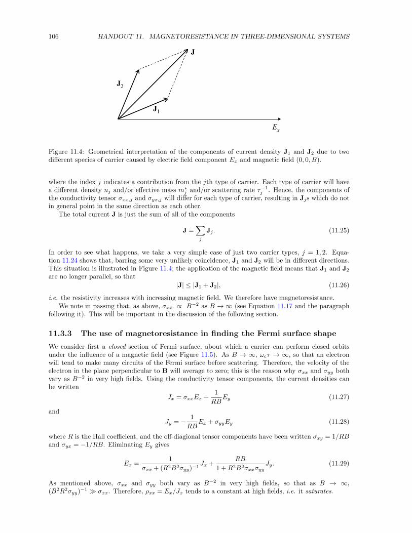
106 HANDOUT 11. MAGNETORESISTANCE IN THREE-DIMENSIONAL SYSTEMS
Ex
J
J2
J1
Figure 11.4: Geometrical interpretation of the components of current density J1 and J2 due to twodifferent species of carrier caused by electric field component Ex and magnetic field (0, 0, B).
where the index j indicates a contribution from the jth type of carrier. Each type of carrier will havea different density nj and/or effective mass m∗j and/or scattering rate τ−1
j . Hence, the components ofthe conductivity tensor σxx,j and σyx,j will differ for each type of carrier, resulting in Jjs which do notin general point in the same direction as each other.
The total current J is just the sum of all of the components
J =∑j
Jj . (11.25)
In order to see what happens, we take a very simple case of just two carrier types, j = 1, 2. Equa-tion 11.24 shows that, barring some very unlikely coincidence, J1 and J2 will be in different directions.This situation is illustrated in Figure 11.4; the application of the magnetic field means that J1 and J2
are no longer parallel, so that
|J| ≤ |J1 + J2|, (11.26)
i.e. the resistivity increases with increasing magnetic field. We therefore have magnetoresistance.We note in passing that, as above, σxx ∝ B−2 as B →∞ (see Equation 11.17 and the paragraph
following it). This will be important in the discussion of the following section.
11.3.3 The use of magnetoresistance in finding the Fermi surface shape
We consider first a closed section of Fermi surface, about which a carrier can perform closed orbitsunder the influence of a magnetic field (see Figure 11.5). As B → ∞, ωcτ → ∞, so that an electronwill tend to make many circuits of the Fermi surface before scattering. Therefore, the velocity of theelectron in the plane perpendicular to B will average to zero; this is the reason why σxx and σyy bothvary as B−2 in very high fields. Using the conductivity tensor components, the current densities canbe written
Jx = σxxEx +1
RBEy (11.27)
and
Jy = − 1
RBEx + σyyEy (11.28)
where R is the Hall coefficient, and the off-diagional tensor components have been written σxy = 1/RBand σyx = −1/RB. Eliminating Ey gives
Ex =1
σxx + (R2B2σyy)−1Jx +
RB
1 +R2B2σxxσyyJy. (11.29)
As mentioned above, σxx and σyy both vary as B−2 in very high fields, so that as B → ∞,(B2R2σyy)−1 σxx. Therefore, ρxx = Ex/Jx tends to a constant at high fields, i.e. it saturates.
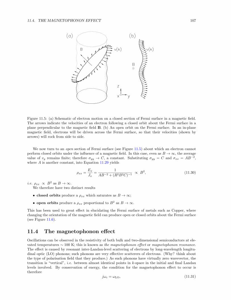
11.4. THE MAGNETOPHONON EFFECT 107
Figure 11.5: (a) Schematic of electron motion on a closed section of Fermi surface in a magnetic field.The arrows indicate the velocities of an electron following a closed orbit about the Fermi surface in aplane perpendicular to the magnetic field B. (b) An open orbit on the Fermi surface. In an in-planemagnetic field, electrons will be driven across the Fermi surface, so that their velocities (shown byarrows) will rock from side to side.
We now turn to an open section of Fermi surface (see Figure 11.5) about which an electron cannotperform closed orbits under the influence of a magnetic field. In this case, even as B →∞, the averagevalue of vy remains finite; therefore σyy → C, a constant. Substituting σyy = C and σxx = AB−2,where A is another constant, into Equation 11.29 yields
ρxx =ExJx
=1
AB−2 + (R2B2C)−1∝ B2, (11.30)
i.e. ρxx ∝ B2 as B →∞.We therefore have two distinct results
• closed orbits produce a ρxx which saturates as B →∞;
• open orbits produce a ρxx proportional to B2 as B →∞.
This has been used to great effect in elucidating the Fermi surface of metals such as Copper, wherechanging the orientation of the magnetic field can produce open or closed orbits about the Fermi surface(see Figure 11.6).
11.4 The magnetophonon effect
Oscillations can be observed in the resistivity of both bulk and two-dimensional semiconductors at ele-vated temperatures ∼ 100 K; this is known as the magnetophonon effect or magnetophonon resonance.The effect is caused by resonant inter-Landau-level scattering of electrons by long-wavelength longitu-dinal optic (LO) phonons; such phonons are very effective scatterers of electrons. (Why? think aboutthe type of polarisation field that they produce.) As such phonons have virtually zero wavevector, thetransition is “vertical”, i.e. between almost identical points in k-space in the initial and final Landaulevels involved. By conservation of energy, the condition for the magnetophonon effect to occur istherefore
jωc = ωLO, (11.31)
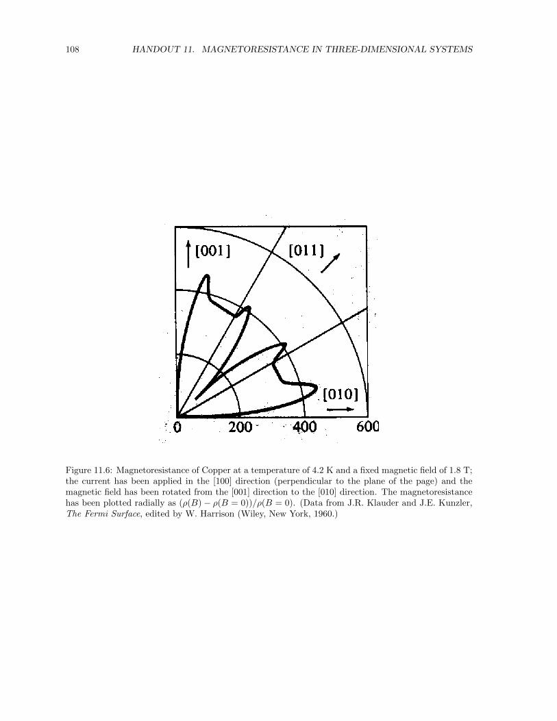
108 HANDOUT 11. MAGNETORESISTANCE IN THREE-DIMENSIONAL SYSTEMS
Figure 11.6: Magnetoresistance of Copper at a temperature of 4.2 K and a fixed magnetic field of 1.8 T;the current has been applied in the [100] direction (perpendicular to the plane of the page) and themagnetic field has been rotated from the [001] direction to the [010] direction. The magnetoresistancehas been plotted radially as (ρ(B)− ρ(B = 0))/ρ(B = 0). (Data from J.R. Klauder and J.E. Kunzler,The Fermi Surface, edited by W. Harrison (Wiley, New York, 1960.)
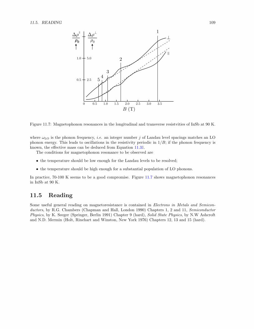
11.5. READING 109
Figure 11.7: Magnetophonon resonances in the longitudinal and transverse resistvities of InSb at 90 K.
where ωLO is the phonon frequency, i.e. an integer number j of Landau level spacings matches an LOphonon energy. This leads to oscillations in the resistivity periodic in 1/B; if the phonon frequency isknown, the effective mass can be deduced from Equation 11.31.
The conditions for magnetophonon resonance to be observed are
• the temperature should be low enough for the Landau levels to be resolved;
• the temperature should be high enough for a substantial population of LO phonons.
In practice, 70-100 K seems to be a good compromise. Figure 11.7 shows magnetophonon resonancesin InSb at 90 K.
11.5 Reading
Some useful general reading on magnetoresistance is contained in Electrons in Metals and Semicon-ductors, by R.G. Chambers (Chapman and Hall, London 1990) Chapters 1, 2 and 11, SemiconductorPhysics, by K. Seeger (Springer, Berlin 1991) Chapter 9 (hard), Solid State Physics, by N.W Ashcroftand N.D. Mermin (Holt, Rinehart and Winston, New York 1976) Chapters 12, 13 and 15 (hard).

110 HANDOUT 11. MAGNETORESISTANCE IN THREE-DIMENSIONAL SYSTEMS
Handout 12
Magnetoresistance intwo-dimensional systems and thequantum Hall effect
12.1 Introduction: two dimensional systems
Lectures 9 and 11 described the effects of a magnetic field on three-dimensional carrier systems; inparticular, Lecture 9 discussed Landau quantisation. We shall now look at two-dimensional semicon-ductor systems in an analogous manner. The two-dimensionality removes one degree of freedom, sothat at high magnetic fields the Landau quantisation results in a density of states consisting entirelyof discrete levels, rather than a series of one-dimensional density-of-state functions. This means thatthe oscillatory phenomena seen in high magnetic fields are often far more extreme in two-dimensionalsystems than they are in the three-dimensional equivalent.
The reduced dimensionality also results in some other novel phenomena; the quantum Hall effect isa general low-temperature property of two-dimensional or quasi-two-dimensional systems and has beenobserved in semiconductor structures (e.g. Si MOSFETs, GaAs-(Ga,Al)As heterojunctions and quan-tum wells containing two-dimensional holes or electrons) and, very recently, in some organic molecularconductors. Most of the research on the quantum Hall effect has been carried out using modulation-doped GaAs-(Ga,Al)As heterojunctions, as these can provide an exceptionally clean two-dimensionalelectron system with a very low scattering rate (see Lecture 8). We shall therefore confine our discus-sion to electrons in GaAs-(Ga,Al)As heterojunctions, although similar principles will apply to any ofthe other systems mentioned above. The effective mass of the electrons in the heterojunction will belabelled m∗, and their areal carrier density Ns.
In a heterojunction, the motion of the electrons in the growth (z) direction is confined by theapproximately triangular potential well at the interface; in this direction, the electrons are in boundstates of the well known as subbands. We let the jth subband have energy Ej . If a magnetic field isapplied in the z direction, then the electrons’ motion in the xy plane will also become quantised intoLandau levels, with energy (l + 1
2 )hωc. Therefore, the total energy of the electron becomes
E(B, l, j) = (l +1
2)hωc + Ej , (12.1)
i.e. the system has become completely quantised into a series of discrete levels.
(We remark at this stage that the magnetic field has reduced the effective dimensionality of theelectron system by two; its density of states is now like that of e.g. an atom, with no electronicdispersion whatsoever. This is a general property of a magnetic field; in the case of a three-dimensionalsystem, the electronic density of states becomes a series of density of states functions for one-dimensionalmotion.)
111
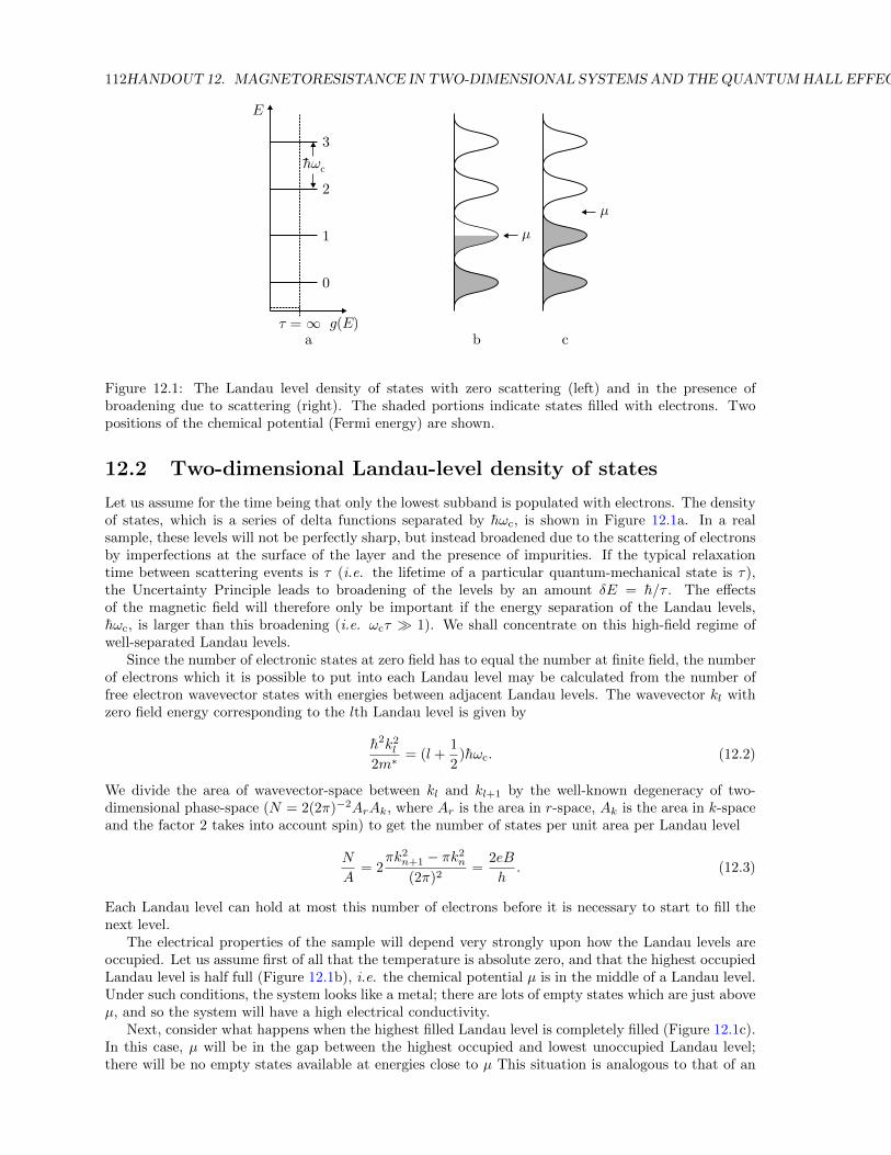
112HANDOUT 12. MAGNETORESISTANCE IN TWO-DIMENSIONAL SYSTEMS AND THEQUANTUMHALL EFFECT
Figure 12.1: The Landau level density of states with zero scattering (left) and in the presence ofbroadening due to scattering (right). The shaded portions indicate states filled with electrons. Twopositions of the chemical potential (Fermi energy) are shown.
12.2 Two-dimensional Landau-level density of states
Let us assume for the time being that only the lowest subband is populated with electrons. The densityof states, which is a series of delta functions separated by hωc, is shown in Figure 12.1a. In a realsample, these levels will not be perfectly sharp, but instead broadened due to the scattering of electronsby imperfections at the surface of the layer and the presence of impurities. If the typical relaxationtime between scattering events is τ (i.e. the lifetime of a particular quantum-mechanical state is τ),the Uncertainty Principle leads to broadening of the levels by an amount δE = h/τ . The effectsof the magnetic field will therefore only be important if the energy separation of the Landau levels,hωc, is larger than this broadening (i.e. ωcτ 1). We shall concentrate on this high-field regime ofwell-separated Landau levels.
Since the number of electronic states at zero field has to equal the number at finite field, the numberof electrons which it is possible to put into each Landau level may be calculated from the number offree electron wavevector states with energies between adjacent Landau levels. The wavevector kl withzero field energy corresponding to the lth Landau level is given by
h2k2l
2m∗= (l +
1
2)hωc. (12.2)
We divide the area of wavevector-space between kl and kl+1 by the well-known degeneracy of two-dimensional phase-space (N = 2(2π)−2ArAk, where Ar is the area in r-space, Ak is the area in k-spaceand the factor 2 takes into account spin) to get the number of states per unit area per Landau level
N
A= 2
πk2n+1 − πk2
n
(2π)2=
2eB
h. (12.3)
Each Landau level can hold at most this number of electrons before it is necessary to start to fill thenext level.
The electrical properties of the sample will depend very strongly upon how the Landau levels areoccupied. Let us assume first of all that the temperature is absolute zero, and that the highest occupiedLandau level is half full (Figure 12.1b), i.e. the chemical potential µ is in the middle of a Landau level.Under such conditions, the system looks like a metal; there are lots of empty states which are just aboveµ, and so the system will have a high electrical conductivity.
Next, consider what happens when the highest filled Landau level is completely filled (Figure 12.1c).In this case, µ will be in the gap between the highest occupied and lowest unoccupied Landau level;there will be no empty states available at energies close to µ This situation is analogous to that of an
12.2. TWO-DIMENSIONAL LANDAU-LEVEL DENSITY OF STATES 113
insulator; the conductivity of the sample will obviously be a minimum under such circumstances, andfor well-separated Landau levels will be effectively zero.
Finite temperatures will cause the Fermi–Dirac distribution function to become “smeared out” closeto µ; however, as long as hωc >∼ kBT , the general picture remains true that the conductivity oscillatesdramatically as the field is swept. The conductivity will be very small whenever we have a completelyfilled highest Landau level, i.e when
Ns = j2eB
h, (12.4)
where j is an integer and Ns is the number of electrons per unit area. The maximum conductivity caseoccurs when
Ns = (j +1
2)2eB
h. (12.5)
The conductivity will therefore oscillate as a function of magnetic field, and will be periodic in 1/B,with a periodicity given by
∆(1/B) =2e
hNs. (12.6)
12.2.1 Resistivity and conductivity tensors for a two-dimensional system
The experimental geometry for the quantum Hall effect is usually exactly the same as that for theconventional Hall effect (see Figure 11.1). Thus, it is the components of the resistivity tensor that wemeasure, and not the conductivity. We can relate the current densities Jx and Jy (in two dimensionscurrent densities will have the units current per unit length) and electric fields Ex and Ey by theexpressions
Jx = σxxEx + σxyEy (12.7)
and
Jy = −σxyEx + σxxEy (12.8)
since σxx = σyy and σxy = −σyx for a homgeneous isotropic substance. If, as usual, we allow a current toflow along only one direction (x) (see Figure 11.1), then Jy = 0 and we can say that Ey/Ex = σxy/σxx.Therefore we can define the resistivities
ρxx ≡ExJx
=σxx
σ2xx + σ2
xy
(12.9)
and
ρxy ≡EyJx
=σxy
σ2xx + σ2
xy
. (12.10)
Note that the units of ρxx are known as Ω per square; a dimensionless geometrical factor (samplelength/sample width) must be introduced to work out the resistance of a particular sample.
We use the Relaxation-Time Approximation to work out the motion of the electrons, i.e.
∂v
∂t= − e
m∗E− e
mv ×B− v
τ. (12.11)
In steady state, the LHS vanishes, and the two components of the equation read
vx = − eτm∗
Ex − ωcτvy (12.12)
and
vy = − eτm∗
Ey + ωcτvx, (12.13)
where we have written ωc = eB/m∗. If we impose the condition vy = 0 (no current in the y direction)we have
EyEx
= −ωcτ. (12.14)
114HANDOUT 12. MAGNETORESISTANCE IN TWO-DIMENSIONAL SYSTEMS AND THEQUANTUMHALL EFFECT
Writing Jx = −eNsvx Equations 12.12 and 12.14 can be combined to give
RH ≡EyJxB
= − 1
Nse. (12.15)
RH is of course the Hall coefficient. Referring to Figure 11.1, we see that for a two-dimensional system,Jx = I/w and Ey = Vy/w, where w is the width of the sample, i.e.
RH =VyIB
. (12.16)
As in the case of the three-dimensional systems discussed previously, the low-field Hall coefficient canbe used to determine Ns.
In high magnetic fields, ωcτ 1. Under these conditions, Equation 12.14 indicates that |σxy| |σxx|, so that Equations 12.9 and 12.10 give
ρxx ≈σxxσ2xy
(12.17)
and
ρxy ≈1
σxy= RHB. (12.18)
We are therefore left with the rather unexpected result that the resistivity is proportional to the con-ductivity. This is due to the very important influence of the Hall field, and the way in which resistivityand conductivity have been defined; the resistivity is defined for zero Hall current, and the conductivityfor zero Hall field.
At the values of magnetic field corresponding to a completely filled highest Landau level, the “in-sulating” case, it is the conductivity σxx which goes to zero, and hence the resistivity ρxx also tends tozero. Physically speaking, what has happened is that, as the probability of scattering goes to zero, anelectron (for Ey = 0) will go around a cyclotron orbit with a drift in a direction perpendicular to theelectric and magnetic fields, and no current will flow along the direction of the applied electric field.For the resistivity (with Jy = 0) the Hall field balances out the Lorenz force, and so a current can flowwith very small scattering probability, giving a vanishing resistivity. Experimentally, ρxx can becomeimmeasurably small.
12.3 Quantisation of the Hall resistivity
Some very interesting things happen when we look at the Hall voltage. Experimentally, at the magneticfield values where ρxx goes to zero, the Hall voltage becomes independent of field, and a plateau appears.When ρxx increases again, then the Hall voltage jumps up to the next plateau. The most interestingfeature of this behaviour is the value of the Hall resistivity on the plateaux. We may calculate this veryeasily.
It was mentioned above that ρxx goes to zero when a whole number of Landau levels are completelyfilled. At this point the density of electrons is (see Equation 12.4)
Ns = j2eB
h(12.19)
And therefore the Hall resistivity is given by
ρxy = RHB =B
Nse=
1
j
h
2e2. (12.20)
As we have seen above (see Equation 12.16), for a truly two-dimensional system the width of the samplecancels out (i.e. ρxy is measured in Ω), so that
ρxy ≡VyI
=1
j
h
2e2=
12906.5
jΩ. (12.21)
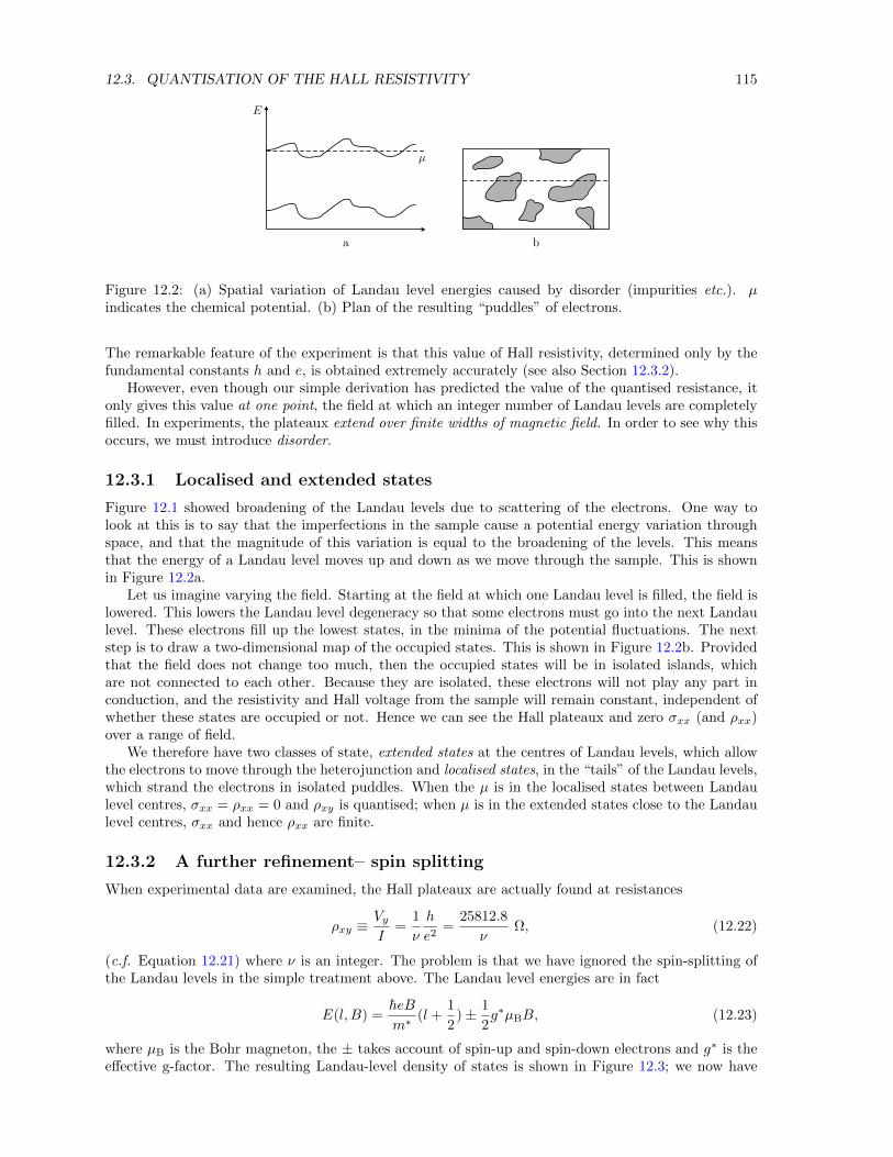
12.3. QUANTISATION OF THE HALL RESISTIVITY 115
Figure 12.2: (a) Spatial variation of Landau level energies caused by disorder (impurities etc.). µindicates the chemical potential. (b) Plan of the resulting “puddles” of electrons.
The remarkable feature of the experiment is that this value of Hall resistivity, determined only by thefundamental constants h and e, is obtained extremely accurately (see also Section 12.3.2).
However, even though our simple derivation has predicted the value of the quantised resistance, itonly gives this value at one point, the field at which an integer number of Landau levels are completelyfilled. In experiments, the plateaux extend over finite widths of magnetic field. In order to see why thisoccurs, we must introduce disorder.
12.3.1 Localised and extended states
Figure 12.1 showed broadening of the Landau levels due to scattering of the electrons. One way tolook at this is to say that the imperfections in the sample cause a potential energy variation throughspace, and that the magnitude of this variation is equal to the broadening of the levels. This meansthat the energy of a Landau level moves up and down as we move through the sample. This is shownin Figure 12.2a.
Let us imagine varying the field. Starting at the field at which one Landau level is filled, the field islowered. This lowers the Landau level degeneracy so that some electrons must go into the next Landaulevel. These electrons fill up the lowest states, in the minima of the potential fluctuations. The nextstep is to draw a two-dimensional map of the occupied states. This is shown in Figure 12.2b. Providedthat the field does not change too much, then the occupied states will be in isolated islands, whichare not connected to each other. Because they are isolated, these electrons will not play any part inconduction, and the resistivity and Hall voltage from the sample will remain constant, independent ofwhether these states are occupied or not. Hence we can see the Hall plateaux and zero σxx (and ρxx)over a range of field.
We therefore have two classes of state, extended states at the centres of Landau levels, which allowthe electrons to move through the heterojunction and localised states, in the “tails” of the Landau levels,which strand the electrons in isolated puddles. When the µ is in the localised states between Landaulevel centres, σxx = ρxx = 0 and ρxy is quantised; when µ is in the extended states close to the Landaulevel centres, σxx and hence ρxx are finite.
12.3.2 A further refinement– spin splitting
When experimental data are examined, the Hall plateaux are actually found at resistances
ρxy ≡VyI
=1
ν
h
e2=
25812.8
νΩ, (12.22)
(c.f. Equation 12.21) where ν is an integer. The problem is that we have ignored the spin-splitting ofthe Landau levels in the simple treatment above. The Landau level energies are in fact
E(l, B) =heB
m∗(l +
1
2)± 1
2g∗µBB, (12.23)
where µB is the Bohr magneton, the ± takes account of spin-up and spin-down electrons and g∗ is theeffective g-factor. The resulting Landau-level density of states is shown in Figure 12.3; we now have
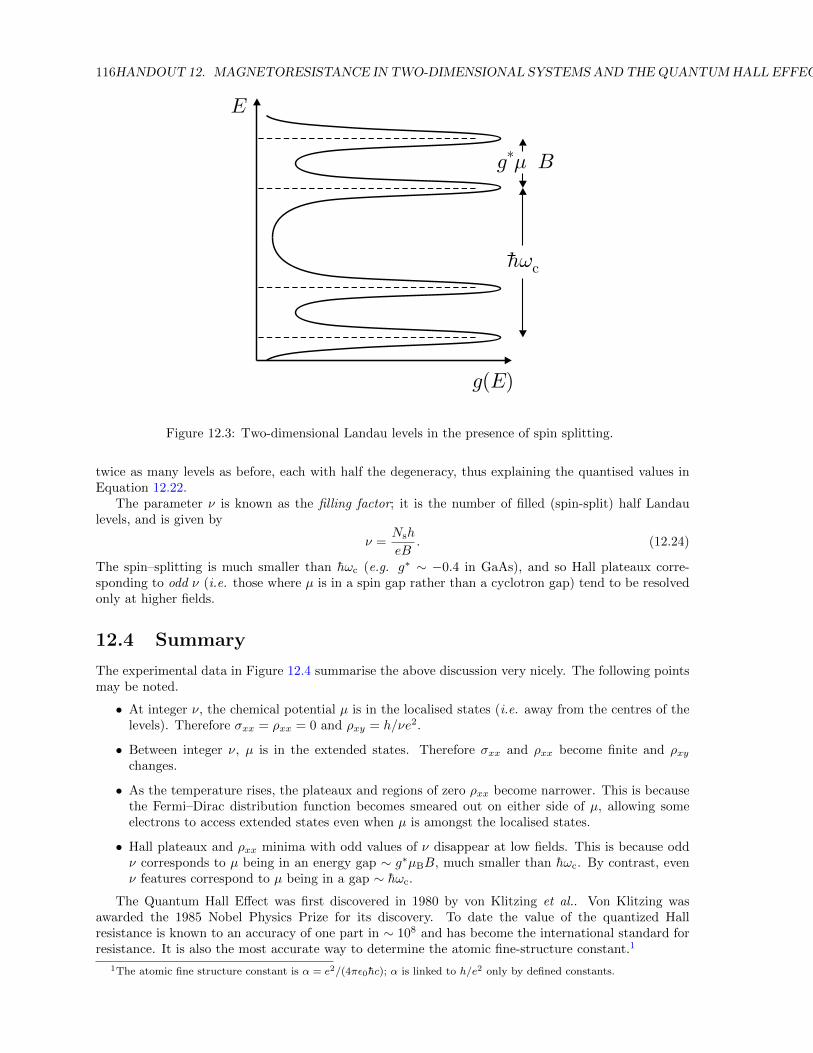
116HANDOUT 12. MAGNETORESISTANCE IN TWO-DIMENSIONAL SYSTEMS AND THEQUANTUMHALL EFFECT
Figure 12.3: Two-dimensional Landau levels in the presence of spin splitting.
twice as many levels as before, each with half the degeneracy, thus explaining the quantised values inEquation 12.22.
The parameter ν is known as the filling factor; it is the number of filled (spin-split) half Landaulevels, and is given by
ν =Nsh
eB. (12.24)
The spin–splitting is much smaller than hωc (e.g. g∗ ∼ −0.4 in GaAs), and so Hall plateaux corre-sponding to odd ν (i.e. those where µ is in a spin gap rather than a cyclotron gap) tend to be resolvedonly at higher fields.
12.4 Summary
The experimental data in Figure 12.4 summarise the above discussion very nicely. The following pointsmay be noted.
• At integer ν, the chemical potential µ is in the localised states (i.e. away from the centres of thelevels). Therefore σxx = ρxx = 0 and ρxy = h/νe2.
• Between integer ν, µ is in the extended states. Therefore σxx and ρxx become finite and ρxychanges.
• As the temperature rises, the plateaux and regions of zero ρxx become narrower. This is becausethe Fermi–Dirac distribution function becomes smeared out on either side of µ, allowing someelectrons to access extended states even when µ is amongst the localised states.
• Hall plateaux and ρxx minima with odd values of ν disappear at low fields. This is because oddν corresponds to µ being in an energy gap ∼ g∗µBB, much smaller than hωc. By contrast, evenν features correspond to µ being in a gap ∼ hωc.
The Quantum Hall Effect was first discovered in 1980 by von Klitzing et al.. Von Klitzing wasawarded the 1985 Nobel Physics Prize for its discovery. To date the value of the quantized Hallresistance is known to an accuracy of one part in ∼ 108 and has become the international standard forresistance. It is also the most accurate way to determine the atomic fine-structure constant.1
1The atomic fine structure constant is α = e2/(4πε0hc); α is linked to h/e2 only by defined constants.
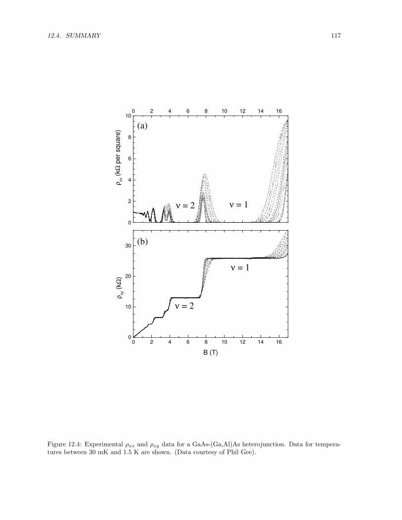
12.4. SUMMARY 117
0 2 4 6 8 10 12 14 160
10
20
30
ν = 2
ν = 1
(b)
ρ xy (k
Ω)
B (T)
0
2
4
6
8
100 2 4 6 8 10 12 14 16
(a)
ν = 2 ν = 1
ρ xx (k
Ω p
er s
quar
e)
Figure 12.4: Experimental ρxx and ρxy data for a GaAs-(Ga,Al)As heterojunction. Data for tempera-tures between 30 mK and 1.5 K are shown. (Data courtesy of Phil Gee).
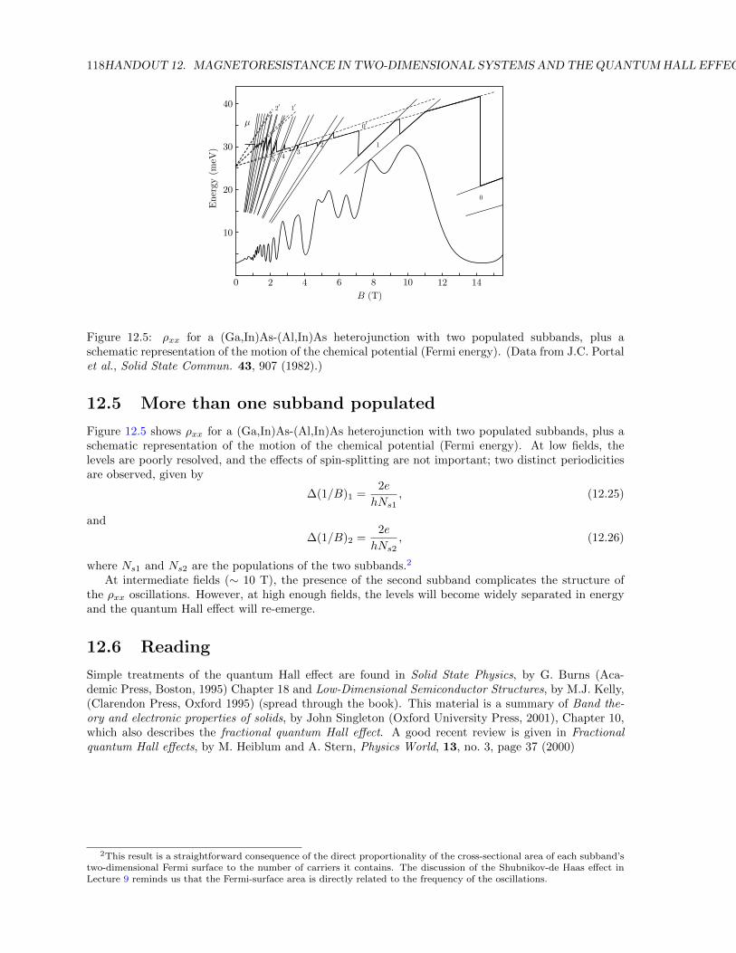
118HANDOUT 12. MAGNETORESISTANCE IN TWO-DIMENSIONAL SYSTEMS AND THEQUANTUMHALL EFFECT
Figure 12.5: ρxx for a (Ga,In)As-(Al,In)As heterojunction with two populated subbands, plus aschematic representation of the motion of the chemical potential (Fermi energy). (Data from J.C. Portalet al., Solid State Commun. 43, 907 (1982).)
12.5 More than one subband populated
Figure 12.5 shows ρxx for a (Ga,In)As-(Al,In)As heterojunction with two populated subbands, plus aschematic representation of the motion of the chemical potential (Fermi energy). At low fields, thelevels are poorly resolved, and the effects of spin-splitting are not important; two distinct periodicitiesare observed, given by
∆(1/B)1 =2e
hNs1, (12.25)
and
∆(1/B)2 =2e
hNs2, (12.26)
where Ns1 and Ns2 are the populations of the two subbands.2
At intermediate fields (∼ 10 T), the presence of the second subband complicates the structure ofthe ρxx oscillations. However, at high enough fields, the levels will become widely separated in energyand the quantum Hall effect will re-emerge.
12.6 Reading
Simple treatments of the quantum Hall effect are found in Solid State Physics, by G. Burns (Aca-demic Press, Boston, 1995) Chapter 18 and Low-Dimensional Semiconductor Structures, by M.J. Kelly,(Clarendon Press, Oxford 1995) (spread through the book). This material is a summary of Band the-ory and electronic properties of solids, by John Singleton (Oxford University Press, 2001), Chapter 10,which also describes the fractional quantum Hall effect. A good recent review is given in Fractionalquantum Hall effects, by M. Heiblum and A. Stern, Physics World, 13, no. 3, page 37 (2000)
2This result is a straightforward consequence of the direct proportionality of the cross-sectional area of each subband’stwo-dimensional Fermi surface to the number of carriers it contains. The discussion of the Shubnikov-de Haas effect inLecture 9 reminds us that the Fermi-surface area is directly related to the frequency of the oscillations.