Embed Size (px)
Citation preview
Lab Manual: Communication Systems Lab (EE-226-F)
B R C M CET BAHAL DEPARTMENT OF ELECTRONICS & COMMUNICATION ENGINEERING Page 1
LAB MANUAL
Communication Systems Lab
(EE-226-F)
Prepared by:
Varun Sharma Dayal C. Sati (Lab In-charge) (Faculty In-charge)

Lab Manual: Communication Systems Lab (EE-226-F)
B R C M CET BAHAL DEPARTMENT OF ELECTRONICS & COMMUNICATION ENGINEERING Page 2
CONTENTS Experiment No-1: To study and Perform Amplitude Modulation & Demodulation. 3-5
Experiment No-2: To study Frequency Modulation and Demodulation. 6-8
Experiment No-3: To study Pulse Amplitude Modulation and Demodulation. 9-10
Experiment No-4: To study Pulse Width Modulation and Demodulation. 11-12
Experiment No-5: To study Pulse Position Modulation and Demodulation. 13-14
Experiment No-6:To study Pulse Code Modulation and Demodulation. 15-17
Experiment No-7: To study Time Division Multiplexing (TDM) system. 18-19
Experiment No-8: To study Amplitude Shift Keying (ASK) Modulation and De-Modulation. 20-21
Experiment No-9: To study Frequency Shift Keying (FSK) Modulation and De-Modulation. 22-24
Experiment No-10: To study Phase Shift Keying (PSK) Modulation and De-Modulation. 25-27

Lab Manual: Communication Systems Lab (EE-226-F)
B R C M CET BAHAL DEPARTMENT OF ELECTRONICS & COMMUNICATION ENGINEERING Page 3
EXPERIMENT NO. – 1 AIM: To study and Perform Amplitude Modulation & Demodulation.
APPARATUS: A.M. Kit, CRO, Connecting Probes.
CIRCUIT DIAGRAM:
Fig.1: AM Modulator
Fig.2: AM De-Modulator

Lab Manual: Communication Systems Lab (EE-226-F)
B R C M CET BAHAL DEPARTMENT OF ELECTRONICS & COMMUNICATION ENGINEERING Page 4
WAVE FORMS:
THEORY: Modulation is the process in which some property of the high frequency wave, also
called as carrier wave c, is altered in such way by low frequency information signal, called as
modulating wave m , to transmit form one place to other place through air. The AM wave is
represented as shown in fig. An its side bands as shown in fig. The top envelope is represented as
Vc + Vm sin mt,
Where the bottom envelope is represented as
- (Vc + Vm sin mt,)
where Vc is the carrier voltage, Vm is the modulating voltage. The ratio between envelope
amplitudes is called as modulation index or factor mf, which is represented as
mf = V max – V min / V max + V min
The value of mf lies between 0 to 1.
The total power in the modulated wave may be expressed as:
Pt = Pc + PLBS + PUSB
Pt = Pc (1+m2 a/2)
PROCEDURE:
Modulation :
1. Connect the circuit as shown on the kit.
2. Connect the CRO probe to the input of modulating signal and see waveform of input
signal on CRO and major its frequency and amplitude.
3. Connect the CRO probe to the output of modulation KIT and see the wave forms for the
modulated signal.

Lab Manual: Communication Systems Lab (EE-226-F)
B R C M CET BAHAL DEPARTMENT OF ELECTRONICS & COMMUNICATION ENGINEERING Page 5
Demodulation :
1. Connect the output received above to the input of demodulating circuit of the kit.
2. Connect the required terminals internally on the kit marked with dotted lines.
3. See the wave for demodulated signal on CRO by connecting the CRO probes on
output of demodulated circuit.
Result: Amplitude Modulation & Demodulation is studied.
Precautions:
1. Switch off the experimental kit during making connections.
2. Set the proper amplitude and frequency of the modulating signal to get a reasonable AM
waveform.
3. Use the CRO carefully.

Lab Manual: Communication Systems Lab (EE-226-F)
B R C M CET BAHAL DEPARTMENT OF ELECTRONICS & COMMUNICATION ENGINEERING Page 6
EXPERIMENT NO. - 2
AIM:. To study Frequency Modulation and Demodulation.
APPARATUS: F.M. Kit, CRO, Connecting Probes.
THEORY:
In frequency modulation, the amplitude of the carrier wave is kept constant but its frequency
is varied in accordance with the amplitude of the audio frequency signal. The phase of the
carrier wave is also kept constant. The instantaneous frequency of the resulting frequency
modulated signal equals,
ωi = ωc + Kf f(t)
The term Kf represents the frequency sensitivity of the modulator.
The instt. frequency of FM signal varies with time. The maximum change in instantaneous
frequency from the average ,i.e., ωc, is known as frequency deviation(Δω).
Δω= Kf Em
CIRCUIT DIAGRAM:
Fig.: FM Modulator
Lab Manual: Communication Systems Lab (EE-226-F)
B R C M CET BAHAL DEPARTMENT OF ELECTRONICS & COMMUNICATION ENGINEERING Page 7
PROCEDURE:
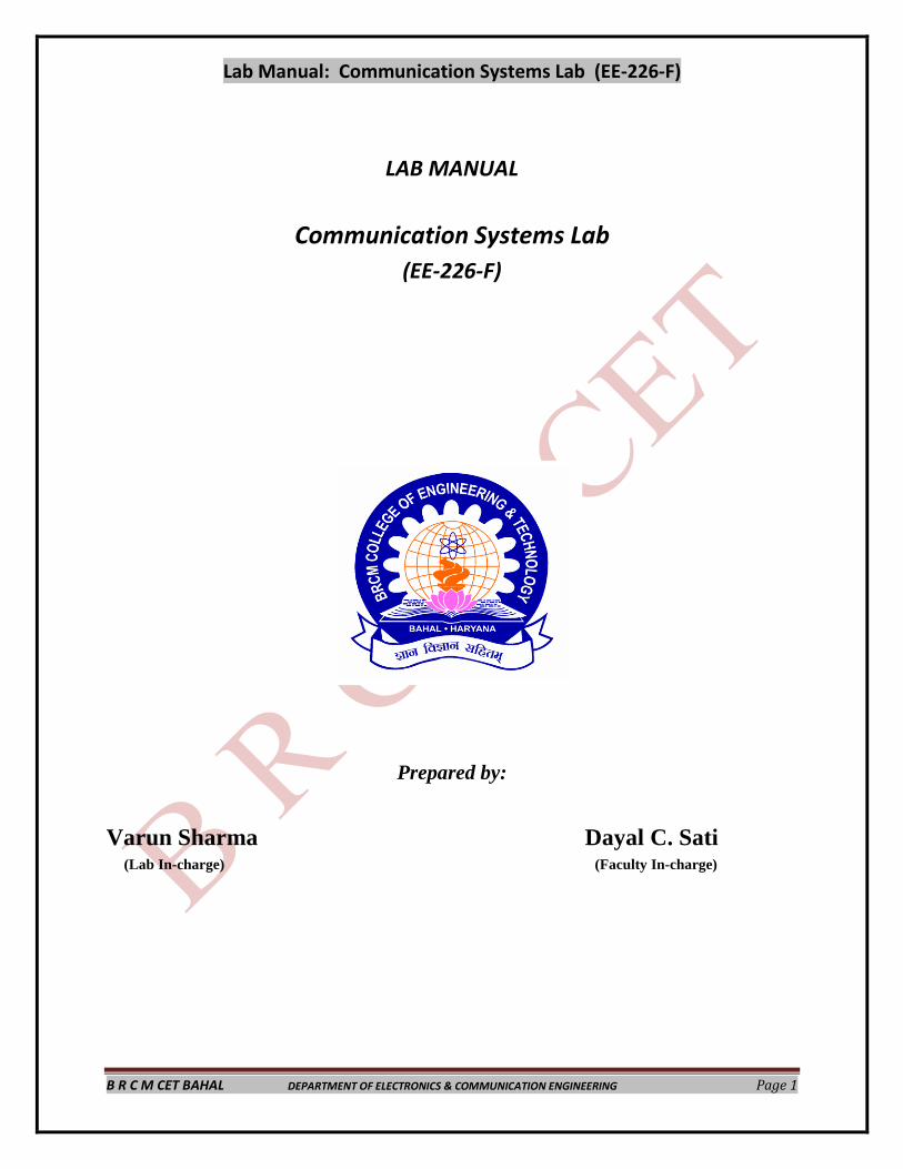
1. Keep amplitude control to maximum. Connect frequency counter at the AC marked
socket of inbuilt 1 KC oscillator and ground socket of Vco circuit to measure its
frequency. Connect CRO in place of counter and observe the AF waveform. Adjust
amplitude control to obtain 1 Vp-p o/p signal.
2. Connect frequency counter across the FM out sockets and measure free run span by
rotating VR control to both extremes.
3. Connect DC o/p of peak rectifier (given in AF oscillator block) with the DC marked
socket. Adjust free run control to 90 KHz and bring AF amplitude control to
minimum. Note the new frequency. Find out the frequency division on one side of
carrier. The total frequency deviation is 2 times of the found frequency since AC
signals has two peaks.
4. Bring free run frequency to lower side e.g. 50 KC. Connect AC o/p socket with AC
i/p socket at Vco. Connect CRO across FM o/p sockets and increase the modulating
voltage.
5. Observe the effect upon the carrier signal. Connect CRO second channel with
modulating signal and adjust time base for single steady waveforms (100s/div).
Expand the trace with X-magnifier and observe the deviation in signal following the
modulating signal polarities.
6. From the observation made, calculation of the modulation index as f/ fm is done. The
FM spectrum is similar to amplitude modulation where the carrier component
depends upon the FM. Calculate the bandwidth, which is equal to (2f + fm).
WAVE FORMS:

Lab Manual: Communication Systems Lab (EE-226-F)
B R C M CET BAHAL DEPARTMENT OF ELECTRONICS & COMMUNICATION ENGINEERING Page 8
Result: Frequency Modulation & Demodulation is studied.
Precautions:
4. Switch off the experimental kit during making connections.
5. Set the proper amplitude and frequency of the modulating signal to get a reasonable FM
waveform.
6. Use the CRO carefully.
Lab Manual: Communication Systems Lab (EE-226-F)
B R C M CET BAHAL DEPARTMENT OF ELECTRONICS & COMMUNICATION ENGINEERING Page 9
EXPERIMENT NO. – 3
AIM: - To study Pulse Amplitude Modulation and Demodulation.
APPARATUS: -Dual trace CRO, PAM kit, Connecting leads.
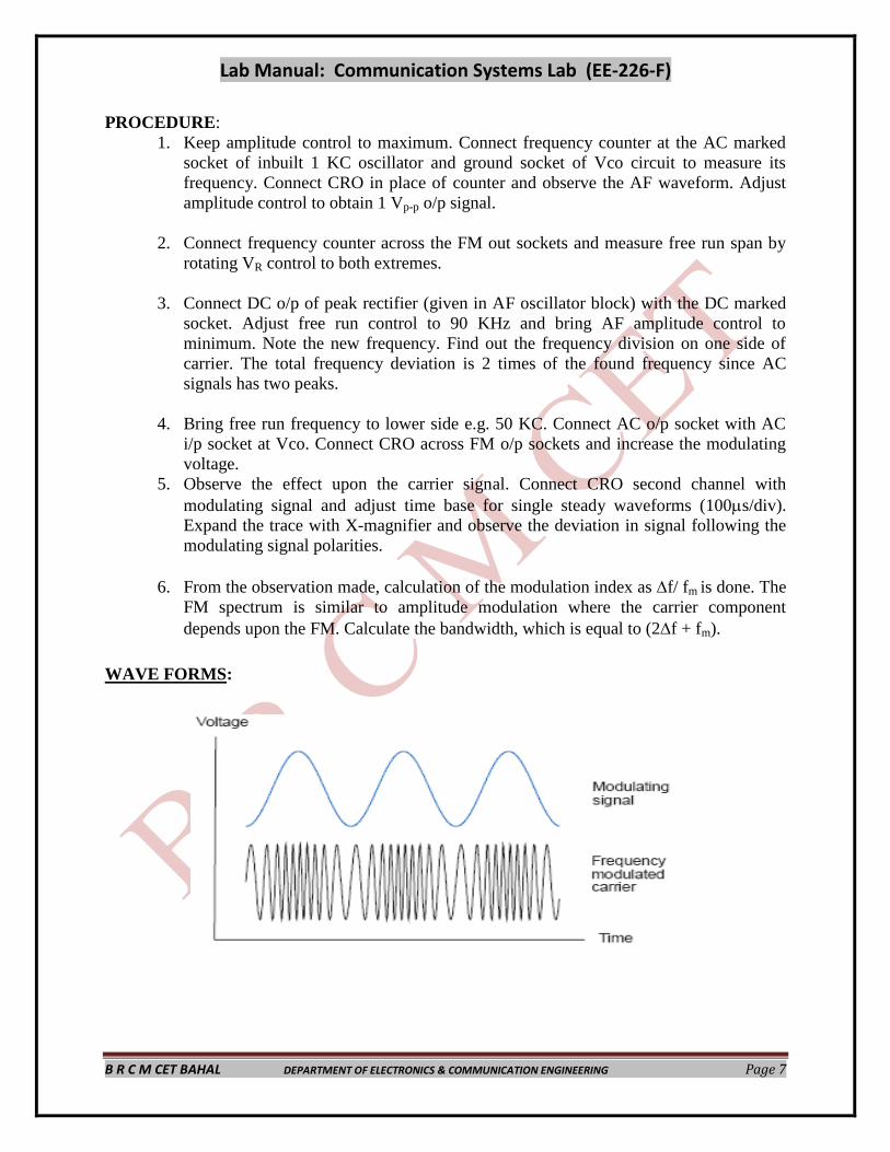
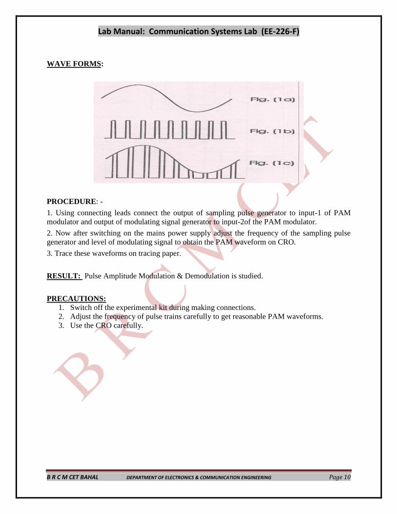
THEORY: - In PAM, amplitude of pulses of carrier pulse train is varied in accordance with the
modulating signal. Fig. explains the principle of PAM. A signal i.e. baseband is shown in fig.
and carrier pulse train fc(t) is also shown. The frequency of carrier train is decided by sampling
theorem. A pulse amplitude modulated signal fm(t) is shown. It can be seen that the amplitude of
pulse depends upon the value of f(t) during the time of pulse.
CIRCUIT DIAGRAM:
Fig.1: PAM Modulator
Fig.1: PAM De-Modulator
Lab Manual: Communication Systems Lab (EE-226-F)
B R C M CET BAHAL DEPARTMENT OF ELECTRONICS & COMMUNICATION ENGINEERING Page 10
WAVE FORMS:
PROCEDURE: -
1. Using connecting leads connect the output of sampling pulse generator to input-1 of PAM
modulator and output of modulating signal generator to input-2of the PAM modulator.
2. Now after switching on the mains power supply adjust the frequency of the sampling pulse
generator and level of modulating signal to obtain the PAM waveform on CRO.
3. Trace these waveforms on tracing paper.
RESULT: Pulse Amplitude Modulation & Demodulation is studied.
PRECAUTIONS:
1. Switch off the experimental kit during making connections.
2. Adjust the frequency of pulse trains carefully to get reasonable PAM waveforms.
3. Use the CRO carefully.
Lab Manual: Communication Systems Lab (EE-226-F)
B R C M CET BAHAL DEPARTMENT OF ELECTRONICS & COMMUNICATION ENGINEERING Page 11
EXPERIMENT NO. - 4
AIM: - To study Pulse Width Modulation and Demodulation.
APPARATUS: -Dual trace CRO, PWM kit, Connecting leads.
THEORY:
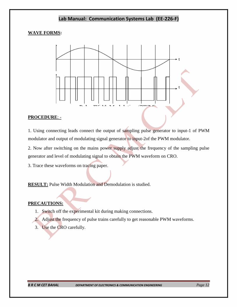
The PWM is also known as pulse duration modulation. It modulates the time parameter of the
pulses. The width of PWM pulses varies. The amplitude is constant; width of the pulse is
proportional to the amplitude of the modulating signal. Bandwidth on transmission channel
depends on rise time of the pulse. The demodulation circuit used is a simple filter circuit that
demodulator the PWM signal and gives the original message input.
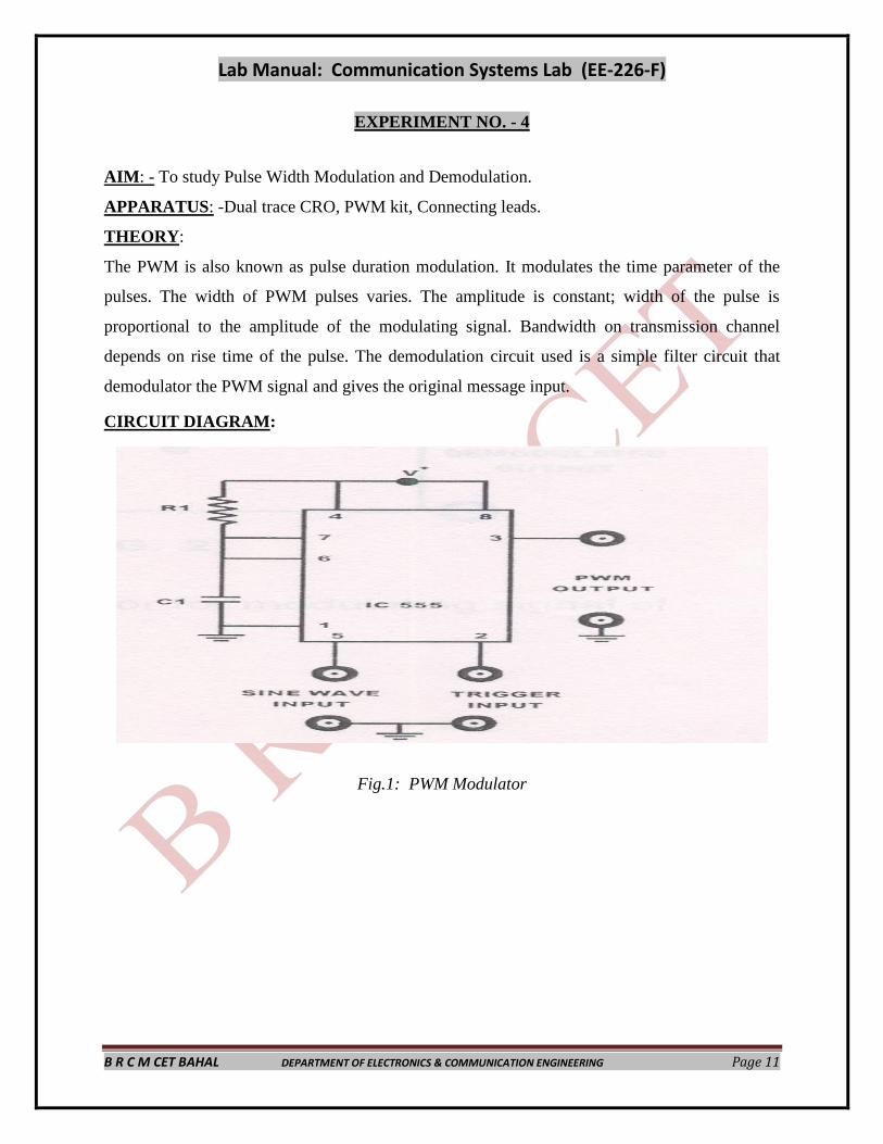
CIRCUIT DIAGRAM:
Fig.1: PWM Modulator
Lab Manual: Communication Systems Lab (EE-226-F)
B R C M CET BAHAL DEPARTMENT OF ELECTRONICS & COMMUNICATION ENGINEERING Page 12
WAVE FORMS:
PROCEDURE: -
1. Using connecting leads connect the output of sampling pulse generator to input-1 of PWM
modulator and output of modulating signal generator to input-2of the PWM modulator.
2. Now after switching on the mains power supply adjust the frequency of the sampling pulse
generator and level of modulating signal to obtain the PWM waveform on CRO.
3. Trace these waveforms on tracing paper.
RESULT: Pulse Width Modulation and Demodulation is studied.
PRECAUTIONS:
1. Switch off the experimental kit during making connections.
2. Adjust the frequency of pulse trains carefully to get reasonable PWM waveforms.
3. Use the CRO carefully.

Lab Manual: Communication Systems Lab (EE-226-F)
B R C M CET BAHAL DEPARTMENT OF ELECTRONICS & COMMUNICATION ENGINEERING Page 13
EXPERIMENT NO. - 5
AIM: - To study Pulse Position Modulation and Demodulation.
APPARATUS: -Dual trace CRO, PPM kit, Connecting leads.
THEORY: -
In Pulse Position Modulation, both the pulse amplitude and pulse duration are held constant but
the position of the pulse is varied in proportional to the sampled values of the message signal.
Pulse time modulation is a class of signaling techniques that encodes the sample values of an
analog signal on to the time axis of a digital signal and it is analogous to angle modulation
techniques. The two main types of PTM are PWM and PPM. In PPM the analog sample value
determines the position of a narrow pulse relative to the clocking time. In PPM rise time of pulse
decides the channel bandwidth. It has low noise interference.
CIRCUIT DIAGRAM:

Lab Manual: Communication Systems Lab (EE-226-F)
B R C M CET BAHAL DEPARTMENT OF ELECTRONICS & COMMUNICATION ENGINEERING Page 14
PROCEDURE: -
1. First observe the waveform of modulating signal (TP2) and carrier signal (TP1) on CRO.
2. Now connect the output of carrier section and modulating signal section to the PPM modulator
section.
3. Switch on Experimental kit.
4. Observe the PPM signal at the output of modulator section (TP3). Adjust the level of the
modulating signal with the pot marked LEVEL in order to obtain a proper PPM signal.
RESULT:- Pulse Amplitude Modulation & Demodulation is studied.
PRECAUTIONS:-
1. Switch off the experimental kit during making connections.
2. Adjust the frequency of pulse trains carefully to get reasonable PPM waveforms.
3. Use the CRO carefully.

Lab Manual: Communication Systems Lab (EE-226-F)
B R C M CET BAHAL DEPARTMENT OF ELECTRONICS & COMMUNICATION ENGINEERING Page 15
EXPERIMENT NO. – 6
AIM: - To study Pulse Code Modulation and Demodulation.
APPARATUS: - PCM kit, Dual trace CRO, Connecting leads.
CIRCUIT DIAGRAM:
Fig. : PCM Modulator
Fig. : PCM De-Modulator
THEORY:
Pulse code modulation pulse code modulation system comprises the following steps:
1. Sampling
2. Quantization
3. Encoding
4. Formatting
Let these four steps should be detailed before circuit description.

Lab Manual: Communication Systems Lab (EE-226-F)
B R C M CET BAHAL DEPARTMENT OF ELECTRONICS & COMMUNICATION ENGINEERING Page 16
1.Sampling:
The input is first sampled according to Nyquist criteria. The Nyquist criteria state that a signal
must be sampled at a rate of >2fm, means the sampling frequency must become than the twice of
input information highest frequency. For a voice signal it must be 2 * 3.4 KHz=>6.8 KHz or say
8 KHz. The sampled signal is now in the form of pulse amplitude modulated signal. Thus in a
pulse code modulation first step is to obtain a PAM signal at Nequist rate.
2. Quantization:
The quantization means to compare the stepped PAM signal height with a known reference
value.
3. Encoding:
The sampled input is compared and encoded into equivalent binary word .Here is to note that a
binary ‘0’ represent absence of pulse and ‘1’ presence of the pulse.
4. Formatting:
The ready data is now transmitted through cables or being modulated by carrier component. Let
take the cable system .To send this data four lines of data stream and one common line is
required .If the encoded data eight word length than there must be nine and lines and it is not
economical same case it is not possible to modulate this data lines (4 & 8) with a carrier
component .Thus prior to send the parallel data is converted into serial form with governing bits.
The process is called data formatting. In the block diagram it is drawn as shown below.
WAVE FORMS:
PROCEDURE: -
1. Keep DC ADJ control to minimum (fully controlled –clock wise).Switch on the
power.

Lab Manual: Communication Systems Lab (EE-226-F)
B R C M CET BAHAL DEPARTMENT OF ELECTRONICS & COMMUNICATION ENGINEERING Page 17
2. Connect the CRO ground with the ground point provided between Tx CK and TX
DO sockets.
3. Connect CRO live lead with the TP1 ,adjust CRO for 2V/div and 1
microsecond/div. Observe the clock signal there. It is the clock signal which is used in
conversion of analog to digital function.
4. Connect the CRO at TP2; adjusting time 50 microsecond/div. It is the main clock
signal which is used performs all functions. Remain CRO one channel connected here.
5. Connect other channel of CRO with the TP3.Observe the signal there. Adjust
CRO time base to appear o ne complete frame upon the signal there .Adjust CRO time
base to appear one complete frame upon the screen.Trace the clock signal with the TP3
signal.
6. .Disconnected TP2 ,probe and connect it with the TP4,TP5, and TP6 signals.Trace
these all signals as shown in the figure.
7. Connect the CRO with the TP7,ehile other input connected with TP3.Observe and
trace this signal.
8. Connect CRO with the TxDO output socket and observe the signal there
9. Trigger CRO with this signal and measure the time T between two successive
leading signals.It is the transmission frame time measure the start bit time.
10. Now increase the analog input (DC ADJ control) signal gradually till
LSB,LED(D0) glows. Observe the modulated signal.
RESULT: Pulse Code Modulation & Demodulation is studied.
PRECAUTIONS:
4. Switch off the experimental kit during making connections.
5. Adjust the frequency of pulse trains carefully to get reasonable PCM waveforms.
6. Use the CRO carefully.

Lab Manual: Communication Systems Lab (EE-226-F)
B R C M CET BAHAL DEPARTMENT OF ELECTRONICS & COMMUNICATION ENGINEERING Page 18
EXPERIMENT NO. - 7
AIM: - To study Time Division Multiplexing (TDM) system.
APPARATUS: Time Division Multiplexing Kit, CRO , Connecting Wires.
DIAGRAM:
Figure: Time division multiplexing Block Diagram
THEORY:
In time division multiplexing, we use the fact that narrow pulses with wide spaces between them
are generated in any of the pulse modulation system, so that spaces can be used by the signal
from other sources. Moreover although the spaces are relatively fixed in width, pulse may be as
narrow as desired, thus permitting the generation of high level hierarchies. There are two types
of time division multiplexing. One is slow speed TDM and other is high speed TDM. Slow speed
TDM is often used in radio telemetry and is produced simply with rotating mechanical switches.
The high speed TDM uses electronic switching and delay lines to accomplish the same result.

Lab Manual: Communication Systems Lab (EE-226-F)
B R C M CET BAHAL DEPARTMENT OF ELECTRONICS & COMMUNICATION ENGINEERING Page 19
PROCEDURE: -
1. Set the duty cycle control switch in position 5.
2. Turn the all potentiometers in Function Generator block fully clockwise.
3. Make the following connections with banana to banana connectors:
250 Hz to CH.0 input socket of TX. block.
500 Hz to CH.1 input socket of TX. block.
1 kHz to CH.2 input socket of TX. block.
2 kHz to CH.3 input socket of TX. block.
4. Turn on the power supply of the trainer.
5. Observe the TX. output along-with CH.0 input for reference with the aid of oscilloscope. The
transmitter circuit samples all channels at different time intervals. The Time Division
Multiplexed samples appear at the TX. output. Vary the amplitude of the input sine-waves by
varying the potentiometers in the function generator block. This will help identifying which
sample belong to which input channel.
RESULT : Time Division Multiplexing and Demultiplexing is studied.
PRECAUTIONS:
1. Switch off the experimental kit during making connections.
2. Use the CRO carefully.
Lab Manual: Communication Systems Lab (EE-226-F)
B R C M CET BAHAL DEPARTMENT OF ELECTRONICS & COMMUNICATION ENGINEERING Page 20
EXPERIMENT NO. – 8
AIM: - To study Amplitude Shift Keying (ASK) Modulation and De-Modulation.
APPARATUS: -, ASK kit, Dual trace CRO, Connecting leads.
CIRCUIT DIAGRAM:-
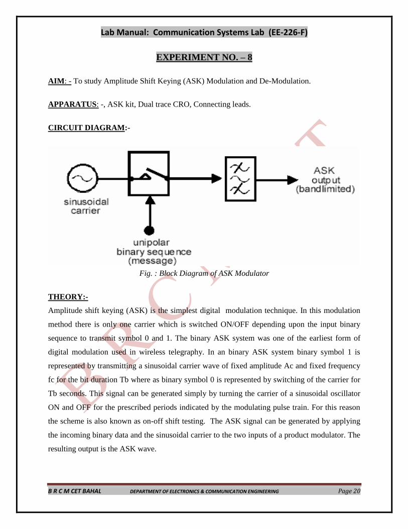
Fig. : Block Diagram of ASK Modulator
THEORY:-
Amplitude shift keying (ASK) is the simplest digital modulation technique. In this modulation
method there is only one carrier which is switched ON/OFF depending upon the input binary
sequence to transmit symbol 0 and 1. The binary ASK system was one of the earliest form of
digital modulation used in wireless telegraphy. In an binary ASK system binary symbol 1 is
represented by transmitting a sinusoidal carrier wave of fixed amplitude Ac and fixed frequency
fc for the bit duration Tb where as binary symbol 0 is represented by switching of the carrier for
Tb seconds. This signal can be generated simply by turning the carrier of a sinusoidal oscillator
ON and OFF for the prescribed periods indicated by the modulating pulse train. For this reason
the scheme is also known as on-off shift testing. The ASK signal can be generated by applying
the incoming binary data and the sinusoidal carrier to the two inputs of a product modulator. The
resulting output is the ASK wave.

Lab Manual: Communication Systems Lab (EE-226-F)
B R C M CET BAHAL DEPARTMENT OF ELECTRONICS & COMMUNICATION ENGINEERING Page 21
WAVE FORMS:
PROCEDURE: -
1. Make connections as per block diagram.
2. Set the input and carrier signal.
3. Obtain ASK modulated and de-modulated signal on CRO and trace it on trace paper.
RESULT: The Amplitude Shift Keying (ASK) Modulation and De-Modulation is studied.
PRECAUTIONS:
1. Switch off the experimental kit during making connections.
2. Set the value of carrier signal precisely.
3. Use the CRO carefully.

Lab Manual: Communication Systems Lab (EE-226-F)
B R C M CET BAHAL DEPARTMENT OF ELECTRONICS & COMMUNICATION ENGINEERING Page 22
EXPERIMENT NO. – 9
AIM: - To study Frequency Shift Keying (FSK) Modulation and De-Modulation.
APPARATUS: -, FSK kit, Dual trace CRO, Connecting leads.
CIRCUIT DIAGRAM:-
Fig. : Block Diagram of FSK Modulator
THEORY:-
Frequency-shift keying (FSK) is a frequency modulation scheme in which digital information is
transmitted through discrete frequency changes of a carrier wave. The simplest FSK is binary
FSK (BFSK). BFSK uses a pair of discrete frequencies to transmit binary (0s and 1s)
information. With this scheme, the "1" is called the mark frequency and the "0" is called the
space frequency. If the incoming bit is 1, a signal with frequency f1 is sent for the duration of
the bit. If the bit is 0, a signal with frequency f2 is sent for the duration of this bit. This is the
basic principle behind FSK modulation.
In the demodulator circuit, the FSK modulated signal is applied to a high Q tuned filter. This
filter is tuned to the frequency of either 0 or 1. This filter passes the selected frequency and
rejects the other.

Lab Manual: Communication Systems Lab (EE-226-F)
B R C M CET BAHAL DEPARTMENT OF ELECTRONICS & COMMUNICATION ENGINEERING Page 23
The output is then passed through a FWR (Full Wave Rectifier) circuit and the output is now
above zero volts only. It is then passed through a comparator; if the input to the comparator is
greater than threshold value, the output is 1, else it is 0. This digital output of the comparator is
the demodulated FSK output.
WAVE FORMS:
PROCEDURE:
(a)Modulation:
1. Connect any one data output of the decade counter to the Data Inputs of the FSK Modulator.
2. Also connect the outputs of carrier generator to the input of Modulator.
3. Switch on the experimental kit.
4. Observe the waveforms at the output of Data Generator and Modulator output using a dual
trace CRO.
5. Repeat the above step for remaining Data also.
(b)Demodulation:
1. Connect the output of the FSK Modulator to the input of the FSK demodulator.
2. Observe the output of the FSK demodulator on the CRO.
3. Adjust the potentiometers provided in demodulator circuit until we get the demodulator output
corresponding to the data input.
Lab Manual: Communication Systems Lab (EE-226-F)
B R C M CET BAHAL DEPARTMENT OF ELECTRONICS & COMMUNICATION ENGINEERING Page 24
RESULT: The Frequency Shift Keying (FSK) Modulation and De-Modulation is studied.
PRECAUTIONS:
1. Switch off the experimental kit during making connections.
2. Use the CRO carefully.
3. Set the values of amplitude and frequencies of oscillators precisely
Lab Manual: Communication Systems Lab (EE-226-F)
B R C M CET BAHAL DEPARTMENT OF ELECTRONICS & COMMUNICATION ENGINEERING Page 25
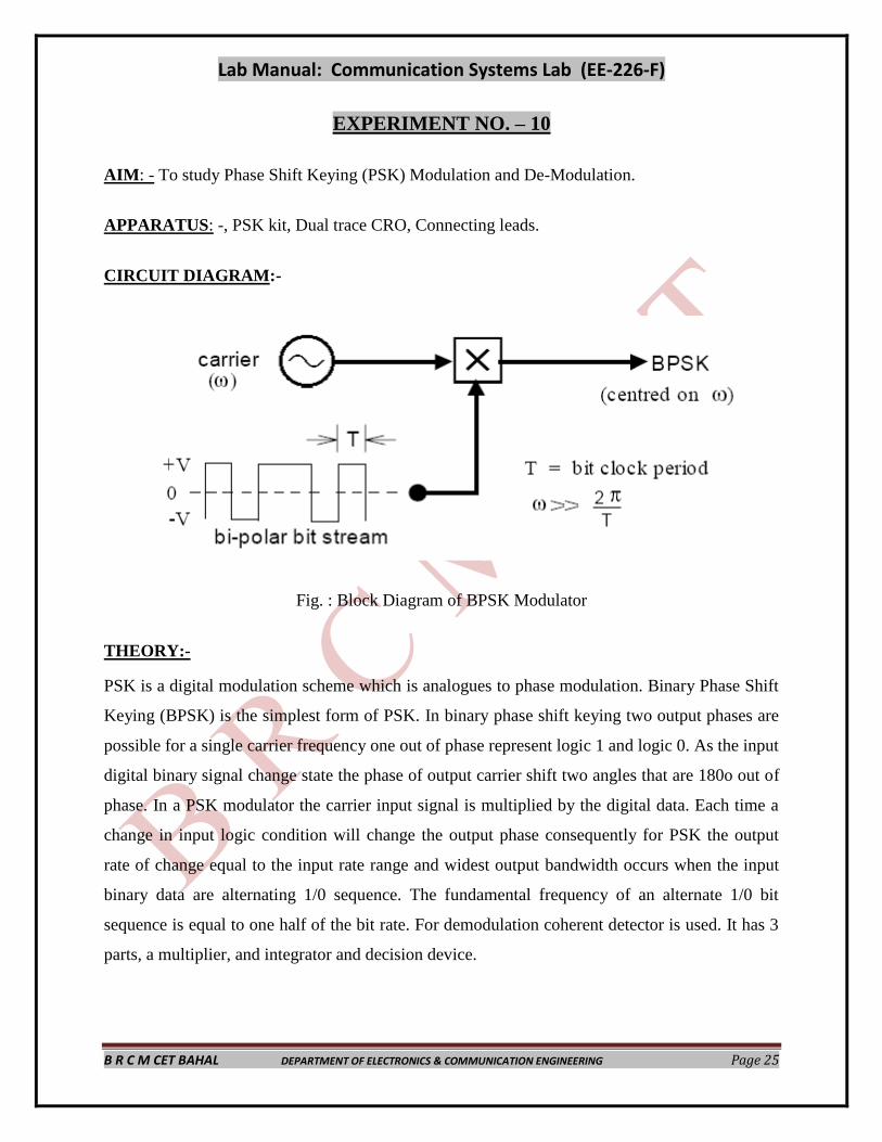
EXPERIMENT NO. – 10
AIM: - To study Phase Shift Keying (PSK) Modulation and De-Modulation.
APPARATUS: -, PSK kit, Dual trace CRO, Connecting leads.
CIRCUIT DIAGRAM:-
Fig. : Block Diagram of BPSK Modulator
THEORY:-
PSK is a digital modulation scheme which is analogues to phase modulation. Binary Phase Shift
Keying (BPSK) is the simplest form of PSK. In binary phase shift keying two output phases are
possible for a single carrier frequency one out of phase represent logic 1 and logic 0. As the input
digital binary signal change state the phase of output carrier shift two angles that are 180o out of
phase. In a PSK modulator the carrier input signal is multiplied by the digital data. Each time a
change in input logic condition will change the output phase consequently for PSK the output
rate of change equal to the input rate range and widest output bandwidth occurs when the input
binary data are alternating 1/0 sequence. The fundamental frequency of an alternate 1/0 bit
sequence is equal to one half of the bit rate. For demodulation coherent detector is used. It has 3
parts, a multiplier, and integrator and decision device.
Lab Manual: Communication Systems Lab (EE-226-F)
B R C M CET BAHAL DEPARTMENT OF ELECTRONICS & COMMUNICATION ENGINEERING Page 26
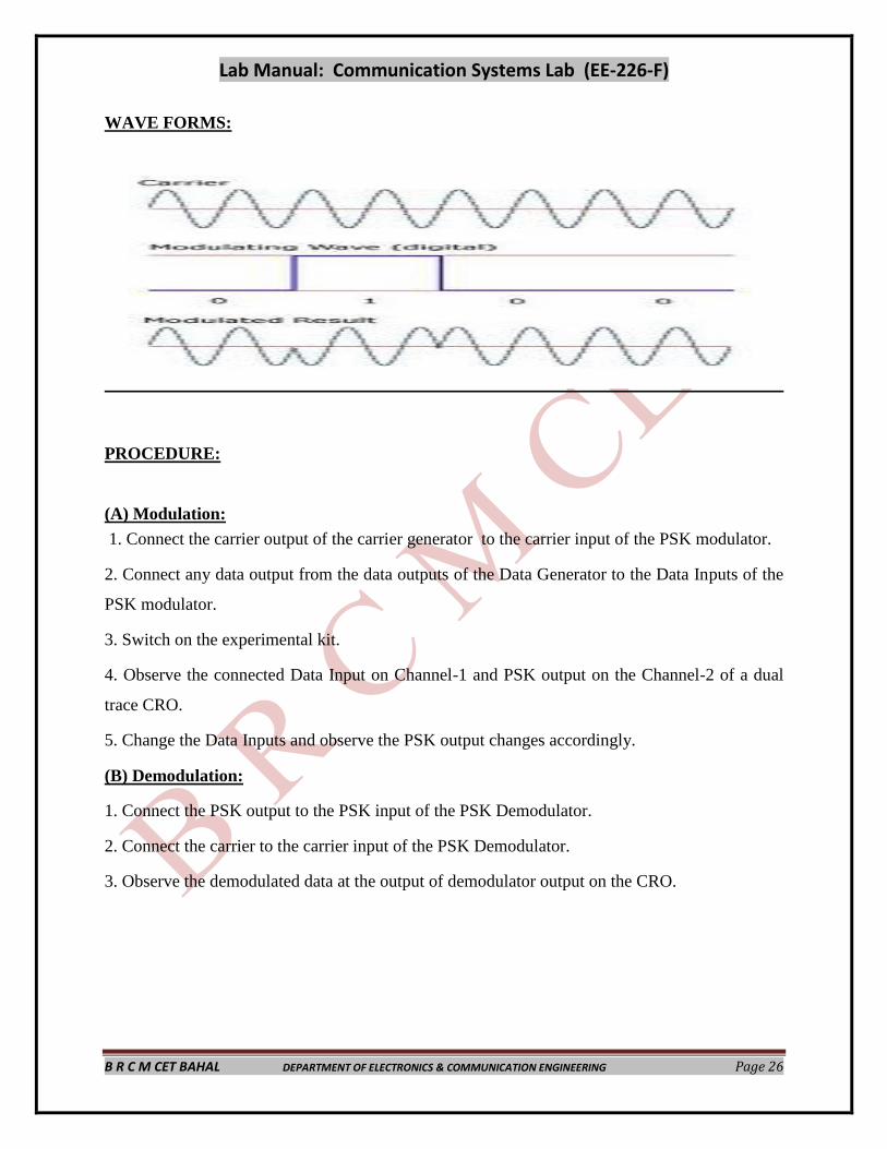
WAVE FORMS:
PROCEDURE:
(A) Modulation:
1. Connect the carrier output of the carrier generator to the carrier input of the PSK modulator.
2. Connect any data output from the data outputs of the Data Generator to the Data Inputs of the
PSK modulator.
3. Switch on the experimental kit.
4. Observe the connected Data Input on Channel-1 and PSK output on the Channel-2 of a dual
trace CRO.
5. Change the Data Inputs and observe the PSK output changes accordingly.
(B) Demodulation:
1. Connect the PSK output to the PSK input of the PSK Demodulator.
2. Connect the carrier to the carrier input of the PSK Demodulator.
3. Observe the demodulated data at the output of demodulator output on the CRO.
Lab Manual: Communication Systems Lab (EE-226-F)
B R C M CET BAHAL DEPARTMENT OF ELECTRONICS & COMMUNICATION ENGINEERING Page 27
RESULT: The Phase Shift Keying (PSK) Modulation and De-Modulation is studied.
PRECAUTIONS:
1. Switch off the experimental kit during making connections.
2. Use the CRO carefully.


![Modulation and Demodulation of Pulse Position Modulation ... · Pulse Position Modulation (PPM) is widely employed in Optical communications [1] and wireless communication [2]. One](https://img.dokumen.tips/doc/110x75/5e9e14ede02fbb6b4309a852/modulation-and-demodulation-of-pulse-position-modulation-pulse-position-modulation.jpg)