Embed Size (px)
Citation preview

Electrical & Computer Engineering: An International Journal (ECIJ) Volume 4, Number 2, June 2015
DOI : 10.14810/ecij.2015.4201 1
COMBINED SKEWED CMOS RING OSCILLATOR
Sadegh Biabanifard1, S. Mehdi Hosseini Largani2 and Shahrouz Asadi3
1,2Microelectronic Lab, Shahid Beheshti University, G. C, Tehran 3Faculty of Electrical Engineering, Shahid Beheshti University, G.C, Tehran
ABSTRACT
A combined skewed ring oscillator by different type of delay stages is presented. This paper aims to drive a
high stable and relatively high frequency but still use a full transistor circuit for ring oscillator with
combined delay stages and skewed connections. First we propose two types of common inverters then
calculate their delay time and analysis their dependence of delay time to variation of power supply voltage.
The simulation results verify that delay time of these two CMOS inverters show opposite behaviour versus
power supply changing. So a combined structure can obtain more appropriate frequency stability versus
power supply noise. Also in order to increase oscillation frequency we have used the negative skewed delay
connections. The simulation results using HSPICE for 0.18 µm CMOS shows a good agreement with
analysis results. In addition in this paper the mathematical justification for improved functioning of this
combined skewed ring oscillator has been proved. This justification shows appropriate agreement with the
simulation results. From mathematical point of view the proposed ring oscillator has better frequency
stability in comparison with other types of ring oscillators. In fact, the oscillation frequency sensitivity to
supply voltage noise is reduced considerably.
KEYWORDS
CMOS, ring oscillator, frequency stability, delay time
1. INTRODUCTION
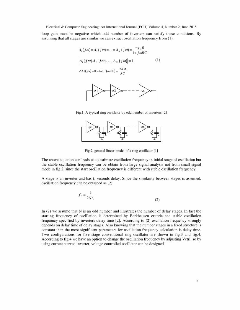
Oscillators are the essential part of any digital and analog systems [1, 11]. And ring oscillator is a circuit usually uses transistors without using passive elements [4]. The main reason of the tendency to design full transistor CMOS circuits is the ability of easy integration with absence of passive elements which reduces the die area [12-20]. The most significant feature of a ring oscillator is lower cost due to lower die area and design simplicity [1, 4, 5]. However the highest possible oscillation frequency is lower for ring oscillators than LC oscillator, negative skewed delay connections can improve the speed of ring type oscillators. Several designs for ring oscillator have been reported in literature. In [1], a frequency stable oscillator is designed based on the opposite direction of delay time changing, which increase frequency stability but oscillation frequency reduce due to using current starved inverter. In [6] a method to enhance frequency operation of ring oscillators by negative skewed delay connections presented. Overall, most of the reported ring oscillators cannot improve both frequency stability and oscillation frequency. In this paper a novel design as combined skewed ring oscillator is presented to improve frequency stability an oscillation frequency simultaneously. Usually a single ended ring oscillator can be implement using odd number of delay stages (Fig.1). Considering oscillation criterion the loop gain must be equal or bigger than unity and also the
Electrical & Computer Engineering: An International Journal (ECIJ) Volume 4, Number 2, June 2015
2
loop gain must be negative which odd number of inverters can satisfy these conditions. By assuming that all stages are similar we can extract oscillation frequency from (1).
( ) ( ) ( )1 2 1
mN
g RA j A j A j
j RCω ω ω
ω
−= = … = =
+
(1) ( ) ( ) ( )1 2. . . 1 N
A j A j A jω ω ω… =
( ) ( )1 2A1 jω θ tan ωRC
K
RC
π−∠ = = =
Fig.1. A typical ring oscillator by odd number of inverters [2]
Fig.2. general linear model of a ring oscillator [1]
The above equation can leads us to estimate oscillation frequency in initial stage of oscillation but the stable oscillation frequency can be obtain from large signal analysis not from small signal mode in fig.2, since the start oscillation frequency is different with stable oscillation frequency. A stage is an inverter and has td seconds delay. Since the similarity between stages is assumed, oscillation frequency can be obtained as (2).
(2) 0
1
2 d
fNt
=
In (2) we assume that N is an odd number and illustrates the number of delay stages. In fact the starting frequency of oscillation is determined by Barkhausen criteria and stable oscillation frequency specified by inverters delay time [2]. According to (2) oscillation frequency strongly depends on delay time of delay stages. Also knowing that the number stages in a fixed structure is constant then the most significant parameters for oscillation frequency calculation is delay time. Two configurations for five stage conventional ring oscillator are shown in fig.3 and fig.4. According to fig.4 we have an option to change the oscillation frequency by adjusting Vctrl, so by using current starved inverter, voltage controlled oscillator can be designed.

Electrical & Computer Engineering: An International Journal (ECIJ) Volume 4, Number 2, June 2015
3
Fig.3. Five stage basic ring oscillator
Fig.4. Five stage Current Starved ring VCO
In this paper we’ve calculated the delay time of basic and Current Starved inverters and based on the equations a combined skewed ring VCO will be presented.
2. DELAY TIME OF INVERTERS
General conditions of ring oscillators were discussed in previous part. In this section delay time calculations are presented since this parameter is the only parameter which can determine the oscillation frequency. By assuming two types of inverters, basic type inverter and current starved inverter (Fig.5).By applying an ideal pulse to both of these inverters, we obtain the output signal depicted in Fig.6. Details of calculations are brought in the appendix A.
2PHL PLH
delayt
τ τ∝
+
2 0PHL t tτ = −
5 3PLH t tτ = −
( )
( )2
2 1L DD
n ox DD th nmos
W
L
PHLbasic
C V
c V V
α
µτ
−
−
−
=
( )
2lnL
n ox DD th nmos
C
Wc V V
L
α β
βµ −
−+
−
(3)
( )2
2 L DD
p ox DD th pmos
W
L
PLHbasic
C V
c V Vµ
γτ
−
−
−
=

Electrical & Computer Engineering: An International Journal (ECIJ) Volume 4, Number 2, June 2015
4
( )
2lnL
p ox DD th pmos
C
Wc V V
L
β
βµ
γ
−
−+
−
( )
( )2
1
2 1L DD
n ox GS th nmos
W
L
PHLCS
C V
c V V
α
µτ
−
−∝
−
( )ln
L
n ox DD th nmos
C
wC V V
L
α β
βµ −
− −
+
(4)
( )2
2
2L DD
p ox SG th pmos
W
L
PLHCS
C V
c V V
γ
µτ
−
−∝
−
( )ln
L
ox DD th pmosp
C
wC V V
L
β γ
βµ −
−+
−
Fig.5. Basic inverter (a) and Current Starved inverter (b)
Fig.6. Input and output of inverters

Electrical & Computer Engineering: An International Journal (ECIJ) Volume 4, Number 2, June 2015
5
In the other word:
1
DD
Basict
V∆ ∝
∆& CurrentStarved DDt V∆ ∝ ∆
As can be seen we can conclude that delay time of these two inverters show different behaviour versus power supply changing. According to (3) and (4) delay time of basic inverter depends on power supply changing in opposite direction which delay time of current starved inverter depends on power supply changing. By considering this fact it is obvious that combined ring oscillator depicted in fig.7 can provide more stable oscillation frequency versus power supply variation. The whole loop delay in this type of oscillator can be introduce as sum of all delay times. In this case first and fifth stages are basic type inverters and other stages are current starved inverters. By summing these delay times the total delay time is less sensitive to power supply variation in comparison with basic type inverter delay time or current starved inverter delay time.
)5( 1 2 3 4 5d d d d dd
t t t t tt = + + + +
Fig.7. Combined ring VCO
Then, if all inverters are the same type , … , will have the same variation. Meaning that all become smaller or bigger. In the other words changing oscillation frequency is inevitable. But in combined structure two types of inverters show opposite behaviours to power supply changing which considerably reduces the dependence of whole circuit to power supply noise. However combined ring VCO has the lower oscillation frequency compared with simple ring oscillators. By using NSD stages we can increase oscillation frequency of combined ring VCO.
3. NEGATIVE SKEWED DELAY SCHEME In conventional inverters both PMOS and NMOS have the same input signals. NSD is a technique that reduces delay of inverters. Fig.8 shows the concept of NSD. In fact in NSD inverter input signal to PMOS arrives earlier than to the NMOS and output changing become faster as illustrated in fig.8.[6]. By using NSD stage to design a ring oscillator we need to modify the connections as shown fig.9. Also for combined ring VCO the circuit of fig.10 is suggested. The minimum number of stages in

Electrical & Computer Engineering: An International Journal (ECIJ) Volume 4, Number 2, June 2015
6
skewed ring oscillator is five because when the number of stage is tree, the skewed ring oscillator yields a PMOS diode- connected load. By using NSD connection for combined ring oscillator we can compensate decreased oscillation frequency by changing configuration.
Fig. 8. NSD inverter
Fig. 9. Skewed ring oscillator
Fig. 10. Proposed Combined Skewed ring VCO

Electrical & Computer Engineering: An International Journal (ECIJ) Volume 4, Number 2, June 2015
7
4. SIMULATION RESULTS In order to validate the previous discussion, five structures in fig.3, fig.4, fig.7, fig.9 and fig.10 have been simulated with HSPICE using TSMC 180 nm technology. The nominal supply voltage and Vctrl have been selected equal to 1.8 V and 1.5 V respectively. Also a factor as frequency deviation is defined in [1] to compare operational performance of simulated circuits. This factor is described in (6).
)6(
( ) ( )( )
DD DD DD
DD
f V V f Vf
f f V
+ ∆ −∆=
In this definition f (VDD+∆VDD) is the oscillation frequency when supply voltage is VDD+∆VDD [1].
Fig. 11 shows frequency deviation factor for five ring oscillator that obtained from simulation. And table.1 presents a comparison between these five type ring oscillators. The simulation results verify the analysis and mathematical justifications since simple combined structure and combined structure with NDS connections show considerable reduction in frequency deviation factor. In addition using NDS connection increases the oscillation frequency for combined ring oscillator from 960MHz to 3.31GHz. The proposed combined skewed ring oscillator is a VCO due to using current starved inverter. Table.1 reports the important parameters for simulated oscillators. According to this table the proposed ring oscillator can work in higher frequencies with lower frequency deviation in compared with simple structures.
Fig. 11. Frequency deviation factor of five ring oscillators.

Electrical & Computer Engineering: An International Journal (ECIJ) Volume 4, Number 2, June 2015
8
Tab. 1. Simulation results for five type ring oscillators
5. CONCLUSION Ring oscillators are one of the basic blocks of integrated circuits. This paper presents two types of CMOS inverters with detailed delay time calculations and then suggests combined structure for implementing an efficient VCO regarding frequency deviation. Oscillation frequency of combined ring VCO is low in respect to simple one. For increasing oscillation frequency we used NSD stages in combined structure that significantly increased oscillation frequency. The results of simulation by HSPICE for 0.18µm CMOS approve the analysis results. According to simulation results the proposed VCO can work in higher frequencies with less frequency deviation. A.1. Appendix A
DD th nmos
DD
V V
Vα −−
=
2DDV
β =
th pmos
DD
V
Vγ −
=
In order to calculate delay time of Basic type inverter (Fig.5 (a)) we can write:
0 1 for t t t nmos saturation< < →
( )21
2Dn n ox in th nmos
WI C V V
Lµ −= − out
CL L
dVI C
dt= − = −
DD th nmos out DD
for V V V V−− < <
0 1DD th nm os DDV V Vα α−− = → < < 1
0
1
DD
DD
t V
L out
Dnt V
dt C dVI
α
=−∫ ∫
Electrical & Computer Engineering: An International Journal (ECIJ) Volume 4, Number 2, June 2015
9
( )
1
0
2
2
wµ
L
DD
DD
t V
Lout
t Vn ox DD th nmos
Cdt dV
C V V
α
−
−=
−∫ ∫
( )
( )0
21
2 1(1 )L DD
n ox DD th nmos
W
L
C Vt A
c V V
tα
µ −
−− =
−
1 2 t t t nmos Linear< < →
( ) 21
2Dn n ox in th nmos out out
WI C V V V V
Lµ −= − −
( ) 21
2out
n ox in th nmos out out L
dVWC V V V V C
L dtµ −− − = −
out DD th
for V V V< − 2
1
1
DD
DD
t V
L out
Dnt V
dt C dVI
β
α
=−∫ ∫
( )
2
1
2
2 1
2
DD
DD
t V
Lout
DD th nmos out outt Vn ox
Cdt dV
W V V V VC
L
β
αµ −
= −− −∫ ∫
( )2 1
2 ln (2 )
L
n ox DD th nmos
CA
WC V V
L
t tα β
βµ −
−=
−
−
( ) ( )2 0 2 1 1 0 PHL
t t t t t tτ ∝ − = − + −
( ) ( )1 2 yields
PHLA A τ+ →
( )
( )2
2 1L DD
n ox DD th nmos
W
L
PHL
C V
c V V
α
µτ
−
−
−
=
( )
2lnL
n ox DD th nmos
C
Wc V V
L
α β
βµ −
−+
−
or
( ) ( )5 3 5 4 4 3 PLH t t t t t tτ ∝ − = − + −
( )2
2L DD
p ox DD th pmos
W
L
PLH
C V
c V Vµ
γτ−
−
−
=
( )
2lnL
p ox DD th pmos
C
Wc V V
L
β
βµ
γ
−
−+
−
Then
31 2 4
DD DD DD DD
Basic
AAAt
V V V
A
V∆ ≅ + + +
∆ ∆ ∆ ∆
Where 1 2 3 4, , ,A A A A , are constant value as follow:
( )1
2 1L
n ox
W
L
C
c
Aα
µ
−=

Electrical & Computer Engineering: An International Journal (ECIJ) Volume 4, Number 2, June 2015
10
22
lnL
n ox
C
Wc
L
Aα β
βµ
−=
3
2 L
p ox
W
L
C
c
A
µ
γ−=
4
2lnL
p ox
CA
Wc
L
β
βµ
γ −=
to calculate delay time of Current Starved inverter (Fig.5(b)) we can write equally.
0 1 t t t< <
[ ] , , in DD out DD DD thV V V V V V∈= −
3 , 1M saturation M saturation→ →
4 M cut off→
DD th nmos out DD
for V V V V−− < <
( )2
1 1
1
2D n ox GS th nmos
WI C V V
Lµ −= −
( )2
1
1
2
Lout
n ox GS th nmos
Cdt dV
wC V V
Lµ −
= −
−
1
0
1
DD
DD
t V
L out
Dnt V
dt C dVI
α
= −∫ ∫
( )1 GS th nmos
Know that V V cte−− =
( )
1
0
2
1
2
w
L
DD
DDGS
t V
Lout
t Vn ox th nmos
Cdt dV
C V V
α
µ −
−=
−∫ ∫
( )
( )1 0
2
1
2 1 (1 )
L DD
n ox GS th nmos
C Vt t B
wC V V
L
α
µ −
−− =
−
1 2 for t t t< <
3 , 1M linear M saturation→ →
( ) 23 3 3 3
1
2D n ox GS th nmos DS DS
wI C V V V V
Lµ −= − −
( )2
1 1
1
2D n ox GS th nmos
wI C V V
Lµ −= −

Electrical & Computer Engineering: An International Journal (ECIJ) Volume 4, Number 2, June 2015
11
3 L
out
C D L
dVI I C
dt≅ − =
out DD th nmos
forV V V −< −
2
1 3
1
DD
DD
t V
L out
Dt V
dt C dVI
β
α
=−∫ ∫
( )
2
12
3 3 3
1
1
2
DD
DD
t V
Lout
t Vn ox GS th nmos DS DS
Cdt dV
wC V V V V
L
β
αµ −
= −
− −∫ ∫
3 1 3 DS out DS out GS in DD
V V V V and V V V= − ≅ ≅ =
( )
2
1
2
1
DD
DD
t V
Lout
DD th nmos out outt Vn ox
Cdt dV
w V V V VC
L
β
αµ −
=−− −∫ ∫
( )2 1
1ln (2 )
L
DD th nmosn ox
Ct t B
w V VC
L
α β
βµ −
−− =
−
( ) ( )2 0 2 1 1 0 PHL
t t t t t tτ ∝ − = − + −
( ) ( )1 2yields
PHLB B τ+ →
( )
( )2
1
2 1L DD
n ox GS th nmos
W
L
PHL
C V
c V V
α
µτ
−
−∝
−
( )ln
L
n ox DD th nmos
C
wC V V
L
α β
βµ −
− −
+
or
( ) ( )5 3 5 4 4 3 PLH
t t t t t tτ ∝ − = − + −
( )2
2
2L DD
p ox SG th pmos
W
L
PLH
C V
c V V
γ
µτ
−
−∝
−
( )ln
L
ox DD th pmosp
C
wC V V
L
β γ
βµ −
−+
−
Then
2 41 3CurrentStarved B B
DD DD
DD DD
t V VV V
B B∆ ≅ ⋅ ∆ + + ⋅ ∆ +
∆ ∆ where 1 2 3 4, , ,B B B B , are constant value as follow:
( )
( )1
2
1
2 1L
n ox GS th nmos
W
L
C
c V V
Bα
µ −
−=
−

Electrical & Computer Engineering: An International Journal (ECIJ) Volume 4, Number 2, June 2015
12
2 ln
L
n ox
C
wC
L
Bα β
βµ
−
=
( )2
2
32 L
p ox SG th pmos
W
L
C
c V V
Bγ
µ −
−∝
−
4 ln p
L
ox
C
wC
L
Bβ γ
βµ
−
=
Or we can write:
1 3 2 4B B B B+ > +
Since
2
, , , ,0 1 1 GS SG th n p GS SG th n p
V V V V− −< − < → − �
( )
( )
( )2
1
2 1 2 1
L L
n ox GS th n ox
C C
w wC V V C
L L
α α
µ µ
− −>
−
( )
( )2
1
2 1 ln
L L
n ox GS th n ox
C C
w wC V V C
L L
α α β
βµ µ
− −>
−
( )2
2
2 ln
L L
p ox th pmos oxSG p
C C
w wC V V C
L L
γ β γ
βµ µ−
− −>
−
Then
1 2 1 4&B B B B> >
3 2 3 4&B B B B> >
So 1 3 2 4B B B B+ > +
In summary
1
DD
Basict
V∆ ∝
∆
CurrentStarved DDt V∆ ∝ ∆

Electrical & Computer Engineering: An International Journal (ECIJ) Volume 4, Number 2, June 2015
13
REFERENCES
[1] G. G. Jovanovi´c, M. Stojˇcev, Z. Stamenkovic. A CMOS Voltage Controlled Ring Oscillator with Improved Frequency Stability. Scientific Publication of the State University of NOVI PAZAR ser. A: APPL. MATH. INFORM. AND MECH. vol. 2, 2010.
[2] B.Razavi. RF Microelectronics. Prentice Hall PTR, 1997. [3] B. Razavi. Design of Analog CMOS Integrated Circuits. MacGraw-Hill,2001 [4] G. Jovanovi´c, M. Stojˇcev. Current starved delay element with symmetric load. International Journal
of Electronics, Vol. 93, 3, 2006. [5] Yao WANG, Jiaxin LIU, Liangbo XIE, Guangjun WEN. An Ultra-Low-Power Oscillator with
Temperature and Process Compensation for UHF RFID Transponder. RADIOENGINEERING, VOL. 22, NO. 2, JUNE 2013, 505-510.
[6] Aimad El Mourabita, Guo-Neng Lub, Patrick Pittetb, A new method to enhance frequency operation of CMOS ring oscillators, International Journal of Electronics, Vol. 99, Issue 3, 2012, 351-360.
[7] Won-tae Leea, Jaemin Shima, Jichai Jeongb, Design of a three-stage ring-type voltage-controlled oscillator with a wide tuning range by controlling the current level in an embedded delay cell. Microelectronics Journal, Volume 44, Issue 12, December 2013, 1328–1335.
[8] Seungjin Kim ; In-Young Lee ; Seok-Kyun Han, A Low-Noise Four-Stage Voltage-Controlled Ring Oscillator in Deep-Submicrometer CMOS Technology. IEEE Transactions on Circuits and Systems. 2013, Vol.60, 71-75.
[9] S. Docking, M. Sachdev. An Analytical Equation for the Oscillation Frequency of High-Frequency Ring Oscillators. IEEE Journal of Solid State Circuits, vol.39, 3, 2004, 533-537.
[10] Yalcin Alper Eken and John P. Uyemura, "A 5.9-GHz voltage-controlled ring oscillator in 0.18- µm CMOS" IEEE J. Solid-State Circuits, vol. 39 no. 1, Jan. 2004.
[11] Ramazani A, Biabani S, Hadidi G, CMOS ring oscillator with combined delay stages. Int J Electron Commun (AEÜ) (2014).
[12] Akbari, M., Biabanifard, S., Asadi, S., & Yagoub, M. C. (2014). Design and analysis of DC gain and transconductance boosted recycling folded cascode OTA. AEU-International Journal of Electronics and Communications, 68(11), 1047-1052.
[13] Largani, H., Mehdi, S., Shahsavari, S., Biabanifard, S., & Jalali, A. (2014). A new frequency compensation technique for three stages OTA by differential feedback path. International Journal of Numerical Modelling: Electronic Networks, Devices and Fields.
[14] Shahsavari, S., Biabanifard, S., Largani, S. M. H., & Hashemipour, O. (2015). DCCII based frequency compensation method for three stage amplifiers. AEU-International Journal of Electronics and Communications, 69(1), 176-181.
[15] Shahsavari, S., Biabanifard, S., Largani, S., & Hashemipour, O. (2014, May). A new frequency compensation method based on differential current conveyor. InElectrical Engineering (ICEE), 2014 22nd Iranian Conference on (pp. 361-365). IEEE.
[16] Akbari, M., Biabanifard, S., Asadi, S., & Yagoub, M. C. (2015). High performance folded cascode OTA using positive feedback and recycling structure. Analog Integrated Circuits and Signal Processing, 82(1), 217-227.
[17] Biabanifard, S., Aghaee, T., & Asadi, S. Adesign GUIDE FOR COMPARATOR-BASED SWITCHED-CAPACITOR INTEGRATOR.
[18] Biabanifard, S., Largani, S. M. H., & Asadi, S. DELAY TIME ANALYSIS OF COMBINED CMOS RING OSCILLATOR.
[19] Largani, S., Shahsavari, S., Biabanifard, S., & Jalali, A. (2014, May). A new SMC compensation strategy for three stage amplifiers based on differential feedback path. In Electrical Engineering (ICEE), 2014 22nd Iranian Conference on (pp. 185-189). IEEE.
[20] Akbari, M., Biabanifard, S., & Hashemipour, O. (2014, May). Design of ultra-low-power CMOS amplifiers based on flicker noise reduction. In Electrical Engineering (ICEE), 2014 22nd Iranian Conference on (pp. 403-406). IEEE.
Electrical & Computer Engineering: An International Journal (ECIJ) Volume 4, Number 2, June 2015
14
AUTHORS
Sadegh Biabanifard was born in Tehran, Iran in 1989. He received the B.Sc. degree in Electronics Engineering from Imam Reza International University, Mashhad, Iran in 2011and M.Sc. degree in Analog Electronics from Shahid Beheshti University, G.C., Tehran, Iran, in 2014. His research interests are RFIC design, analog and mixed mode integrated circuits design for Ultra-Low-Power Ultra-Low-Voltage applications, OTA, current conveyer and data converter.
S. Mehdi Hosseini Largani was born in Tonekabon, Iran in 1989. He received the B.S. degree in Control Engineering from K.N.Toosi University of Technology, Tehran, Iran in 2011 and M.S. degree in Analog Electronic from Shahid Beheshti University (National University of Iran) G.C., Tehran, Iran, in 2014. His research interests are analog and mixed mode circuit theory, integrated circuit design for Ultra-Low-Power Ultra-Low-Voltage applications. His is currently with Electrical Engineering Department and Microelectronic Research Laboratory in Shahid Beheshti University, G.C, Tehran, Iran.
Shahrooz Asadi received the B.Sc. degree in Electrical Engineering and the M.Sc. degree in Electronics both from Amirkabir University, Tehran, Iran, in 2003 and 2007, respectively and the Ph.D. degree in Electronics in the School of Information Technology and Engineering (SITE), University of Ottawa, Ottawa, ON, Canada. He joined shahid Beheshti University in 2011 where he is an assistant professor. His research interests include linear and nonlinear time-domain modeling of millimeter-wave transistors, RF design of active and passive devices, design and optimization of solid state devices and multiconductor transmission lines and printed circuit board.