Embed Size (px)
Citation preview

COHERENT PLASMON COUPLING IN SPHERICAL METALLODIELECTRIC
MULTILAYER NANORESONATORS
by
CHARLES ALAN ROHDE
A DISSERTATION
Presented to the Department of Physicsand the Graduate School of the University of Oregon
in partial fulfillment of the requirementsfor the degree of
Doctor of Philosophy
September 2008

11
University of Oregon Graduate School
Confirmation of Approval and Acceptance of Dissertation prepared by:
Charles Rohde
Title:
"Coherent Plasmon Coupling in Spherical Metallodielectric Multilayer Nanoresonators"
This dissertation has been accepted and approved in partial fulfillment of the requirements forthe Doctor of Philosophy degree in the Department of Physics by:
Jens Noeckel, Chairperson, PhysicsMiriam Deutsch, Member, PhysicsGregory Bothun, Member, PhysicsMichael Raymer, Member, PhysicsJeffrey Cina, Outside Member, Chemistry
and Richard Linton, Vice President for Research and Graduate Studies/Dean of the GraduateSchool for the University of Oregon.
September 6, 2008
Original approval signatures are on file with the Graduate School and the University of OregonLibraries.

iii
An Abstract of the Dissertation of
Charles Alan Rohde
in the Department of Physics
for the degree of
to be taken
Doctor of Philosophy
September 2008
Title: COHERENT PLASMON COUPLING IN SPHERICAL
METALLODIELECTRIC MULTILAYER NANORESONATORS
Approved:Dr. Miriam Deutsch
In this thesis we theoretically and experimentally investigate the subwavelength
manipulation of light with nano-scale patterned metallodielectric resonators. By
coupling light to surface plasmon excitations, we calculate the modified dispersion
relation of the resulting surface plasmon polartion (SPP) modes in two types of
subwavelength resonators: (i) closed, spherical micro-resonators with nano-scale metal
dielectic-metal shells; (ii) periodic, metal-dielectric-metal-layered silica surfaces.
We show theoretically that with the proper geometric parameters, one can use sub
wavelength structure on spherical surfaces to manipulate the SPP dispersion relation
in a highly tunable fashion. A tunable avoided-crossing of plasmonic dispersion
bands is found to be the result of the coherent near-field coupling of silver nano-shell
SPP modes. By developing our own stable computational algorithms, we calculated

iv
the far-field scattering of these metal-dielectric-metal layered micro-resonators. We
demonstrate that the near-field interaction of the SPPs leads to a tunable, SPP
induced transparency in the composite particle's scattering and extinction cross
sections.
Utilizing finite element calculations, periodically-modulated metal-dielectric-metal
layers are shown to alter the transmission properties of plasmon enhanced transmission
through their support of interior surface plasmon (ISP) modes. Our simulations
indicate that, subwavelength silver-silica-silver trilayers coating arrays of silica cylinders
support ISP modes analogous to those found in spherical metal-dielectric-metal shells.
We examine the coupling between ISP and radiating SPPs, and find the possibility
of efficient free-space coupling to ISP modes in planar geometries. Further, the
excitation of these ISP modes is found to predicate plasmon enhanced transmission,
adding directionality and refined frequency selection.
Experimentally, we show that self-assembled monolayers of silica spheres form
a novel substrate for tunable plasmonic surfaces. We have developed a deposition
method to conformally coat these hexagonal-close-packed substrates with nano-scale
silver-polystyrene-silver coatings. We use angle-resolved spectroscopy to study their
transmission properties. We have discovered that the presence of the silver-polystyrene
silver layer supports the excitation of ISP modes, and that these excitations significantly
alter the plasmon enhanced transmission. Finally, we have discovered that the use of
the ordered monolayers as a plasmonic substrate can create a new effect in conjunction

v
with plasmon enhanced transmission: directionally asymmetric transmission. This is
demonstrated with optically thick silver coatings evaporated upon onto the ordered
sphere monolayers.
CURRICULUM VITAE
NAME OF AUTHOR: Charles Alan Rohde
PLACE OF BIRTH: Saginaw, Michigan
DATE OF BIRTH: May 10, 1977
GRADUATE AND UNDERGRADUATE SCHOOLS ATTENDED:
University of Oregon, Eugene, OregonMichigan Technological University, Houghton, Michigan
DEGREES AWARDED:
Doctor of Philosophy in Physics, 2008, University of OregonMaster of Science in Physics, 2005, University of OregonBachelor of Science in Physics, 2000, Michigan Technological University
AREAS OF SPECIAL INTEREST:
Optics, Photonics, and Plasmonics.
PROFESSIONAL EXPERIENCE:
Graduate Research Assistant,University of Oregon, 2001 - 2008
Post-baccalaureate Student InternLos Alamos National Laboratory, 1999-2001
Undergraduate Research AssistantMichigan Technological University, 1997-1999
VI
GRANTS, AWARDS AND HONORS:
National Science Foundation, Integrative Graduate Education and Research Traineeship Fellow (2002)
Los Alamos National Laboratory Distinguished Performance Team Award(2000)
LANL Nonproliferation and International Security Division Student Scholarship (1999)
National Merit Scholarship Finalist (1995)
PUBLICATIONS:
Charles Rohde, Keisuke Hasegawa, and Miriam Deutsch, Optics Letters32, 415 (2006).
Keisuke Hasegawa, Charles Rohde, and Miriam Deutsch, Optics Letters31, 1136 (2006).
C. A. Rohde, K. Hasegawa, and Miriam Deutsch, Physical Review Letters96, 045503 (2006).
Charles Rohde, Keisuke Hasegawa, Aiqing Chen, and Miriam Deutsch,Materials Research Society Symposium Proceedings 846 (2005).
Vll

viii
ACKNOWLEDGEMENTS
I would like to thank the following people who labored with me or or by my side
as I have struggled to achieve. Thank you to my parents Charles and Diana Rohde,
and to my siblings Julia, Cynthia, and David Rohde; to my friends both old and
new(er): Brian Weeden, Natasha Sefcovic, Alysia McLain, Aaron Morrison, Brock
Bose, Danniel Cassel, and "da' Man Ranch"; thank you to the influential teachers
in my life: Dan Sealey, Gary Barker, Rose Nickodemous, William Slough, and Bob
\iVeidman; to my research colleagues (both in and out of school): Keisuke Hasegawa,
Eric Hoffmann, Larwarence "Mick" Davis, and Peter Erslev; and finally, a thank you
the mentors and advisors that have most strongly influenced the direction of my work
and my professional life: Ken Flurchick, Bruce Rafert, Anthony Davis, and Miriam
Deutsch.

IX
This thesis is dedicated to my better (though too often, distant) half: Amy C. Mills.

x
TABLE OF CONTENTS
Chapter Page
I. INTRODUCTION........................................................ 1
Historical Context and Introduction 1Modern Use and Research of SPPs. . . . . . . . . . . . . . . . . . . . . . . . . . . . . . . . . . . . . . . .. 6The Motivation for Investigating SPPs on Curved Surfaces 17Thesis Outline 19
II. BASIC THEORY OF SURFACE PLASMON POLARITONS 22
Dielectric Function of Metals 22Bulk Plasmons 24Surface Plasmons at Flat Interfaces 25Coupling to Surface Plasmons 26SPP-SPP Coupling in Flat MD Trilayers 29
III. THEORY OF METALLODIELECTRIC MIE SCATTERING 33
Introduction 33Localized SPPs on Small Spheres 33Mie Theory: Beyond the Quasistatic Approximation 37SPP-SPP Coupling in MD Shells 40Discrete Computation of Field Coefficients 44
IV. PLASMON COUPLING IN MDM SPHERES 48
Introduction 48MDMd Particle Band Structure 49Plasmon Induced Transparency 56Multiple Shells: M(DM)x 60Conclusions 63
V. FINITE ELEMENT ANALYSIS OF PERIODIC MDM SURFACES 65
Introduction 65

Chapter
Xl
Page
ISP Mode Parity 69ISP-ESP Coupling in Modulated MDM Layers 71ISP Control of SPP Enhanced 'Transmission 74Conclusions 79
VI. FABRICATION OF PERIODIC MDM COATINGS 80
Introduction 80Monodisperse Silica Spheres 80Isothermal Monolayer Self-Assembly 84MDM Layer Deposition 88MDM Layer Characterization 91
VII. ANGLE RESOLVED SPECTROSCOPY OF MDM COATINGS 95
Introduction 95Design and Alignment of an Angle Resolved Spectrometer 96AR Spectrometer Calibration 101Scattering from Silver Coated Opal Monolayers 105MDM Coated Opal Monolayers 109Asymmetric 'Transmission 113Conclusions 117
VIII. CONCLUSIONS 118
Future Work 122Concluding Remarks 124
APPENDICES 126
A. CALCULATION OF MULTILAYERED SPHERICAL PARTICLES 126
Single Spherical Scatter 126MDm Cavities and DMd Core-Shell Particles " 132MDMd TM Mode Equation 133Asymptotic Expansion of VMd 137
B. RECURSIVE CALCULATION OF SPHERICAL SCATTERING 139

Chapter
Xll
Page
C. FElVI ANALYSIS OF PERIODIC PLASMONIC STRUCTURES 144
Setup of FEM Model 144MATLAB Band Diagram Script 151
BIBLIOGRAPHY 156

Xlll
LIST OF FIGURES
Figure Page
1.1 Papers with the topic of "plasmons," as retrieved from, and analyzedwith, the lSI Web of Knowledge database. [7] (blue curve) analysis islimited to lSI's physics and optics subcategories. The difference from thetotal can mainly be attributed to the use of plasmonic sensors in the lifesciences. (inset) Log of physics and optics publications illustrating thescale break correlated with the start of the study of plasmons in coherentnano-optics. Blue lines are linear fits to the data from 1986-1996 andfrom 2000-2007 2
1.2 Schematic comparison of (a) a DMD strip SPP waveguide to a (b) MDMSPP waveguide. The strip guide has a propagation length on the order ofcentimeters, and weak confinement perpendicular to the metal interface(2:: 5,um). MDM SPP waveguides have propagation lengths rv 100,umand perpendicular confinement rv Ao/10. 9
1.3 A slab of negative index material reconstructs point sources in the nearfield with resolution greater than the diffraction limit. The refractedwave-vector into a negative index material remains on the same side ofthe surface normal as the incident wave-vector. A conventional materialrefracts on the opposite side of the surface normal. 11
1.4 Dispersion relations for SPPs on air-silver and air-silica interfaces. Alsoplotted are the light lines in air k = w/ c and silica k = nsilicaW / c.klight < k spp reflecting the bound nature of SPP modes, and their smallereffective wavelength 17
2.1 Comparison between Drude-Sommerfeld model for fm(W) and empiricallycollected data for silver from Palik [58] 24
2.2 The dispersion relation w(ksp ) for two interfaces: air-silver and silica-silver, using the Drude-Sommerfeld model and tabulated values 27
2.3 Grating coupling to normally incident plane waves. (a) Simple gratingand planewave geometry (b) H-field intensity (color map) and E-field intensity (contours) of the air-silica plasmon resonance (c) reflection spectrum exhibiting silica-silver (1.4 eV, 886nm) and air-silver (1.97 eV,629nm) SPP resonances 28
2.4 Principle reciprocal lattice vectors of a hexagonal lattice: GrK = 47f /3aand GrM = 27f / V3a, superimposed on the hcp structure with latticeconstant a 29

Figure
XIV
Page
2.5 Coupling of two surfaces supporting surface plasmon excitations::::} C2 ex-[1,3' The mode splitting will exist for both dielectric slabs (MDM) ormetal films (DMD) structures 30
3.1 Plasmonic particle types and our abbreviated nomenclature: (a) Metalsphere, embedded in a dielectric medium (Md) (b) dielectric void (Dm)(c) one or more metal-dielectric shells (DMd, MDm, MDMd, (MD)xd,etc. . 34
3.2 (a) Calculated extinction cross-section efficiencies of r = 10nm silverand gold spherical nanoparticles using tabulated dielectric functions. (b)Comparison of gold nanoparticle extinction, scattering, and absorptionscattering efficiencies showing the dominate absorption of nano-scale par-ticles. (c) Comparison of silver particle in water vs. air. 36
3.3 (a) Spherical scatterer with N shells each with index ofrefraction yEi andradius ri, embedded in a medium with index of refraction v!cN+l. (b)Specific types of single and double shell particles which we will addresslater in this chapter. 39
3.4 The scattering cross-section efficiency as a function of size parameter foran absorbing soot covered water droplet. (Left) Results of W. Yang [87].(Right) Computation of Qsca using our algorithm 46
3.5 Comparison of EM field algorithm. (a) E-field intensity from Lecler etal. [89] compared with (b) our computation for a large silica sphere. (c)E and H field intensities from Wang et al. [92] compared with (d) for asmall metal sphere with [ = -2 + 0.2'i 47
4.1 Examples of the geometry and composition of the metal and dielectric(Md, MDm and MDMd) resonators studied in this chapter. 49
4.2 (a) TM mode, angular dispersion for a Drude-silver/titania MDm withrl = 500 nm and L = L* (b) Total absorption cross-section of a geometrically optimized MDMd particle created from titania and silver shells.(c) Individual angular mode (£) absorption cross-sections showing thesimultaneous excitation of rv 12 modes (red hashes). Reproduced withpermission from [82] 51
4.3 Angular mode dispersions of (!VID)x microspheres. The MDMd spheresdiffer in their outer shell thicknesses (a) T = 7 nm, (b) T = 28 nm, and(c) T = 70 nm. Also plotted are bands of Md (n = 0) and MDm (n = 1)particles respectively labeled as ISP and ESP. The mode distributions atthe locations denoted by the open, blue circles will be discussed furtherbelow. Their mode energy distributions will be used to define interiorand exterior plasmon modes 54

Figure
xv
Page
4.4 Near-field energy density plots for the modes indicated by the open bluecircles in figure 4.3, at (a) ( W/Wp = 0.336, £. = 10 ), (b) ( w/wp = 0.294,£. = 6) and (c) (w/wp = 0.233, £. = 7) 55
4.5 (a) (Ext)inction, (sca)ttering and (abs)orption cross-section efficienciesfor a solid metal sphere with 7"3 = 584 nm. (b) Scattering cross-sectionfor a MDMd plasmonic particle as compared to two other constituentgeometries (Md and DMd) described in the text. The figures in the plotlegend are drawn to scale 56
4.6 Total near-field energy densities for Ao = (c) 407nm (w/wp = 0.336), (b)463nm (w/wp = 0.294), (c) 586nm (w/wp = 0.233). All incident fieldsare described by plane-waves with k-vector k = 21r/ Ao impinging fromthe left 57
4.7 (a) Comparison of the scattering cross-sections of a MDMd particle anda Md sphere with equivalent scattering area at 463 nm. (b) Comparisonof the angle resolved scattering (inset) between a MDMd particle and asolid Md sphere with the same total radius. . 58
4.8 Tuning the (a) scattering, and (b) extinction transparency window withdielectric shell width, L. Second order transparencies indicated withblack arrows. (c) Tuning of absorption resonance accompanying thechange of L 59
4.9 Dispersion diagrams for several MDMDm silver/titania plasmonic cavities. The dark lines form the solutions to the eigenmode equation ex-tended from equation (III.18) 60
4.10 Scattering cross-sections of multilayered MDMDMd particles. (a) Overlap of two forward scattering transparencies from a double DM shell.(b) Overlap of the first order and second order scattering transparenciesfrom an asymmetric double DM layered particle. Black arrows indicatethe created split transparency windows, and red arrows indicate the destructive interference of the original particles' level coupled resonatorinduced transparency 62
5.1 Sketch of the cylindrically modulated MDM geometry: (top) coordinatesystem of a TM (p-polarized) plane-wave scattering from the infiniteMDM grating with the plane of incidence oriented perpendicular to thegrating plane-wave A = 21r / a. (bottom) Geometric parameters of theMDM coating, S = 30nm, L = 100nm, T = 15nm. The colors blue(silica) and gray (silver) indicate the material composition 66

Figure
XVI
Page
5.2 (left) Geometry and free mesh of the computational domain used in thisstudy. (right) Total energy density plots of (a) an interior surface plasmonmode (kx = 0, W = 1.54PHz). (b) an external surface plasmon mode(kx = 0.5, W = 1.57PHz). (c) a localized substrate plasmon mode(kx = 0,W = 1.97PHz) 68
5.3 (left) Band diagram overlaid upon normal absorption (log(l- (7 +R)))of the periodic MDM coating of figure 5.2. The line style indicates thedominant mode character at kx = 0: ISP (solid), ESP (dashed), SSP(dotted) and its color indicates parity: black (even) and gray (odd). (c)Absorbance vs. frequency cross-section plots at three values of k x indicating the strong excitation of ISP (kx = 0.22) and ESP-ISP hybridized(kx = 0.36) modes " 70
5.4 Cross-sectional plot of the electric field energy density through an MDMcoating at the position of 96% efficiency ISP generation (kx = 0.22,W = 1.76PHz) 72
5.5 Change in central resonance frequency of k x = 0.22 ISP resonance asa function of tln = nino, where no = 1.42. Error bars indicate theresonance full width half maximum (FWHM). A one percent change inthe index of refraction is sufficient to shift the central frequency by theresonance FWHM. . 73
5.6 Transmission through (a) the MDM silver-silica-silver of figure 5.2 and(b) silica-silver (DM) coating coating created by removing the top silverlayer from the geometry shown in figure 5.2 75
5.7 Cross-sectional plots of the electric field energy density through an MDMcoating for varied incident angles around ISP enhanced transmissionmaxima (kx = 0.23, W = 2.67PHz) 76
5.8 (left) Band diagram overlaid upon normal absorption of a a = 300nmMDM coating. This geometry supports a localized, dispersionless plasmon cusp mode near W = 3.37PHz (560nm). (right) Magnetic andElectric field distributions of (a) the localized cusp mode at (kx = 0,Wk = 3.37PHz) and (b) the LSP/EPS/ISP hybrid mode at (kx = 0.40,W = 3.3 PHz). The filled contour plot is the Hz magnitude, and thearrows are proportional to E = Exx + Eyf/ '" 78
6.1 (a) Measured size distribution and (b) SEM image of Stober reaction 5. . .. 826.2 (a) Measured size distribution and (b) TEM image of Stober reaction 9.... 836.3 Diagrams of (a) evaporative self-assembly process and (b) the isothermal-
heating evaporative self-assembly (IHESA) chamber built to grow vertically deposited opal monolayers. (c) A picture of the IHESA chamber,before the addition of the evaporation filtration pump 84

Figure
XVll
Page
6.4 Examples of silver coated opal monolayers with a variety of sphere radii:(a) 200nm (b) 250nm (c) 285nm (d) 250nm (e) 285nm. The glasssubstrates are cut to 5/8" x 3/4". Second layer striping manifests asdarker regions and speckle 87
6.5 (a) An SEM images of silver coated opals taken at 5 kV. (a) showinga typical line defect across its length. Note that the dark spots areimaging artifacts due to surface charging, and not crystal defects. (b) ahigh magnification image of a typical point defect from a small sphere.Both opals are coated with 50 nm of silver. 88
6.6 Calibration of spin coat rotation speed vs. polystyrene layer thickness.The layer thickness and standard deviation are shown for two substrates(silver and silica) using 4% by weight polystyrene in toluene. Leastsquared fits to exponential functions are also shown. . 90
6.7 AFM images of (a) silver-polystyrene, and (b) silver coated monolayeropals. Inset are line profiles of the highlighted paths 92
6.8 SRM images of silver-polystyrene-silver coated opal monolayers. (a) AnMDM layer near an open area in the HCP monolayer, with the red arrowindicating the crystal growth direction. (b) High magnification image of abreak in the MDM layer caused by an underlying line defect terminatingin a missing sphere point defect. (b) also shows the suspended nature ofthe polystyrene layer over the silver coated opal. The polystyrene doesnot fill the interstitial voids of the crystal monolayer. 93
6.9 SEM images of the long range order of the HCP monolayers. Silverpolystyrene-silver coatings are shown capping the opal monolayer. Thepolystyrene layer is seen to fail at defect sites in the underlying crystal. 93
7.1 Schematic layout of angle resolved spectroscopy system. . 967.2 Detailed illustration of the angle resolved sample holder, the fiber-coupled
collection optics, and the sample inspection microscope 987.3 (a) Coordinate system of an oriented sample in the AR spectrometer.
(b) Geometry of a periodic MDM based on a self-assembled monolayerof silica spheres. Blue is silica, gray is silver, and yellow is polystyrene.The system is embedded in air. 101
7.4 Normalization of input signal, and chromatic correction for non-identicaldetectors. The resulting signal has a noise level of less than 0.005 at650 nm 102
7.5 (left) Zero-order AR transmission through a flat 50 nm thick silver film.(right) Zero-order AR transmission through uncoated opal 83 « R > =285 nm) 103

Figure
xviii
Page
7.6 (left) Zero-order AR transmission through a polystyrene and silver coatedmonolayer opal 83 (L = 100nm, T = 20nm), (right) overlaid with theanomalous diffraction from the air-silver interface (green line) 104
7.7 SPP enhanced zero-order transmission at 750nm (2.51 PHz) from a silver coated (5 = 70 nm) opal monolayer as described in the text. This iscompared to an uncoated opal monolayer, and the transmission througha fiat,50 nm thick, silver film. All spectra were taken with our AR spec-trometer at normal incidence 106
7.8 (left) AR zero-order transmission of opal 57B. A 5 = 70nm silver coatedopal. (right) The zero-order transmission with anomalous diffraction(green) and [0 1] silver-silica grating SPP dispersion (red) overlays 107
7.9 (left) AR zero-order transmission of opal 57A. An MDM coated opal withL = 140nm. Red arrows indicate ISP extinction. (right) The zero-ordertransmission with [0 1] and [0 2] grating SPP dispersion bands for asilver-silica (red) and a silver-polystyrene interface (blue). The silver-airanomalous diffraction is plotted with green dots 109
7.10 (left) AR zero-order transmission of opal 60. An MDM coated opal withL = 160 nm. Red arrows indicate ISP extinction. (right) The zero-ordertransmission with [0 1] and [0 2] grating SPP dispersion bands for asilver-silica (red) and a silver-polystyrene interface (blue) 110
7.11 (left) AR zero-order transmission of opal 64. An MDM coated opal withL = 125 nm. Red arrows indicate ISP extinction. (right) The zero-ordertransmission with [0 1] and [0 2] grating SPP dispersion bands for asilver-silica (red) and a silver-polystyrene interface (blue) 111
7.12 Asymmetric zero-order transmission from silver coated opal 57B. (left)¢ = 0°, (right) ¢ = 180°. Both graphs are plotted on the same scale asfigure 7.8. . 114
7.13 (a) Symmetric zero-order transmission through silver coated opal 86.Also plotted is the asymmetric zero-order transmission from MDM opal84 for (b) ¢ = 0°, and (c) ¢ = 180°. The color scales of (b) and (c) aremagnified by a factor of 5 with respect to (a). . 115
B.1 Geometry and labels of an L shell system 139C.1 (left) Geometry and free mesh of the computational domain used in this
study. (right) Total energy density plots of (a) an interior surface plasmonmode (k x = 0, W = 1.54PHz). (b) an external surface plasmon mode(k x = 0.5, W = 1.57PHz). (c) a localized substrate plasmon mode(kx = 0,W = 1.97PHz) 145

Figure
xix
Page
C.2 (a) Comparison of FEM with analytic calculation for normal transmission and reflection through (a) a 27nm thick silver film in air and, (b)asymmetrically (top) and conformally (bottom) modulated sinusoidal silver films from [125]. (c) E-field intensity comparison with Schroter [125]at ru.u = 1.97 eV. The reflectivity dip at 1.97 eV shows the excitation ofa SPP on the air-silver interface. . 150

xx
LIST OF TABLES
Table Page6.1 Stober reaction constituent molarities for synthesizing monodisperse sil-
ica spheres in ethanol. The resulting sphere average diameters and stan-dard deviations are also given. (.) t indicates active cooling 81
6.2 Typical deposition parameters for crystallization of opal monolayers.Vacuum levels were held at 6.25" Hg for all reactions, and "S Rxn"cross-references the table 6.1 reaction numbers. The deposition time isgiven in hr:mins 86
7.1 Geometry of opals presented in this study. The thicknesses L are esti-mates based on the calibration curve in figure 6.6 112

1
CHAPTER I
INTRODUCTION
Historical Context and Introduction
In this thesis, we examine the interaction of light 1 with structured metal surfaces
which vary on scales much smaller than that of the external free space wavelength
(AO)' In this, we are part of a new optics frontier, bringing manipulation of light
down to length scales on the order of tens of nanometers. This is made possible by
the existence of bound surface waves, called surface plasmon polaritons (SPP) at the
interfaces between metal and insulating materials. This revolution in the way we think
about controlling light waves has been brought about by the substantial advances in
the fabrication of nano-scale metallic surface features, modern optical characteriza-
tion techniques, the availability of powerful computational tools, and an increasing
pressure to create nanoscale integrated devices [1]. In this thesis, we will utilize all of
these enabling aspects to study the effects of coherent coupling of SPP surface waves
on and between spherical and hemispherical metal-dielectric (MD) interfaces.
For approximately one-hundred years, studying the interaction of electromagnetic
1Note that "light" in this work refers to electromagnetic radiation in the visible and near-infraredregions of the electromagnetic spectrum (400nm-lOOOnm). Other electromagnetic spectral regionswill be denoted with their conventional labels: microwaves, terahertz, etc.

2
(/)
c: 3000 . Total Plasmon Publications.9..... Phys. and Optics Plasmon Publ icationsro 2500.~ ~, ::;?l Subwavelength::0 Plasmonsic Plasmonic Nano-Optics
i::l 2000i ,.~
Biosensors 1998p., :g n~ t4-<
1500 ~"r :.--' · 1999 I 19900....
! J(l)
..0 1000
~::l: JE j::l 500 -Z --' ,,,. ,.,.,
0 ,1970 1980 1990 2000
Year
Figure 1.1. Papers with the topic of "plasmons," as retrieved from, and analyzedwith, the lSI vVeb of Knowledge database. [7] (blue curve) analysis is limited tolSI's physics and optics subcategories. The difference from the total can mainly beattributed to the use of plasmonic sensors in the life sciences. (inset) Log of physicsand optics publications illustrating the scale break correlated with the start of thestudy of pl(),smons in coherent nano-optics. I31u<~ lines are line(),r i1ts to the dat(), from1986-1996 and from 2000-2007.
(EM) radiation at the interface of metals and insulators has piqued the interest of
many physical-scientists. Over the past two decades there has been an explosion in the
amount of research contributed to this i1eld, i1gure 1.1. From their beginnings, these
investigations have been driven by a wealth of possible applications, and have been
made possible by technological advances in our ability to manipulate the structure
of metal-insulator interfaces on an ever decreasing size scale. From its theoretical
foundations (Sommerfeld [2], Zennek [3], and Mie [4]) and its experimental beginnings
(Wood [5] and Farady [6]) has sprung the modern i1eld of surface plasmon polaritons:
the coupling of the EM field and th(~ nano-structured metallic surfaces of today's most
advanced materials science technologies.

3
Delocalized Surface Plasmon Polaritons
Central to the optical study of nano-structured metal surfaces is the coherent
excitation of the conduction electrons at the metal-insulator interface. The earli-
est theoretical work on this concept is generally considered to be Sommerfeld's and
Zennek's studies of radio frequency surface waves along finite conductivity wires and
planes. Experimentally, in 1902 Wood found "most remarkable" [5] the rapid intensity
variation in some spectral emission lines, upon reflection from the surface of a metal-
lic grating. Nearly forty year later, Wood's "almost incomprehensible" [5] anomalous
diffraction was brought together with Sommerfeld's bound surface wave by Fano [8].
This work combined the coupling of the freely propagating EM wave continuum with
radiating surface currents at optical frequencies. Finally, Ritchie [9] linked this pre-
vious work and that of thin film electron electron loss spectroscopy [10, Il] bringing
together and solidifying the field of bound surface waves at metal-insulator interfaces
under the single rubric of surface plasmon polaritons (SPP). 2
As will be discussed more formally in chapter II, the high mobility of a metal's (es-
sentially free) conduction electrons allows excitation of ensemble plasma oscillations
against the restoring force of the ionic lattice background. Provided that both energy
and momentum are conserved, these coherent oscillations can be excited with both
charged particle bombardment and external EM waves. In this thesis, we are only
concerned with the subset of oscillations that exist exclusively at the metal surface
2Although it is only in the context of surface plasmons coupled to EM-fields that the addendumpolariton is added, this is the exclusive condition under which we will be operating in this work.

4
that are referred to as surface plasmons (in opposition to the bulk plasmon excita
tion). These SP excitations are bound to the metal-insulator interface, and as such
they possess a maximum electromagnetic field intensity at the interface and evanes
cently decay into the adjacent media. The decay lengths of these exponential tails
are on the order of tens of nanometers on the the metal side of the interface and on
the order of hundreds of nanometers on the insulator side. Because they are confined
to dimensions smaller than the free space wavelength in the single dimension per
pendicular to the interface, the lack of confinement in the remaining two dimensions
allows the SPPs to freely propagate along the surface. As such, this class of SPP
excitations are referred to as delocalized. This distinguishes them from localized SPP
excitations, where variations in the interface nanoscale geometry further restrict the
SPP decay length in all three dimensions.
Localized Surface Plasmons
Since the seminal work of Mie in 1908 [4], it has been recognized that metal
particles with small radii (with respect to an incident wavelength, r « Ao) support
resonant modes that result in very large absorption. This phenomenon can be at
tributed to localized surface plasmons, and it can be observed in every-day contexts
such as the color of artisan stained glass and some ceramic glazes. Since Roman times,
it has been known that mixing metals such as silver and gold with glasses, ceramics,
and dyes can add spectacular color to the work [12]. In 1857, Faraday [6] was the first
to purposely create pure colloidal suspensions of monodisperse gold nanoparticles for

5
optical investigation. When viewed in transmission, these colloidal solutions exhibit
the rich red color indicative of the localized gold plasmon dipole resonance. 3 It is
due to the very small size of the gold particulates (r rv IOnm) that the solution color
is no longer "gold." The lowest order spherical absorption resonance for IOnm gold
nanoparticles is centered in the green part (500nm, c.f. chapter III) of the optical
spectrum. The green absorption thus results in the weighted transmission of red light.
As will be examined in detail in chapter III when the metal particles become
larger, and/or are coated with additional shells of insulating and metallic materials,
this simple picture of dipole plasmon excitation becomes much more complicated. By
implementing an extend form of Mie's curvilinear scattering theory we will explore
the effects on SPP coupling by multi-shell plasmonic particles whose radii are on the
same scale as that of the incident EM wavelength. This will lead us to several fas-
cinating effects, including nano-engineered coatings that can induce both enhanced
electromagnetic absorption, narrow frequency scattering transparencies. We will also
go beyond ]'v1ie's scattering theory, and its multi-shell extensions, to examine theo-
retically and experimentally the effects of thin, fractal, silver shells on the spherical
surface plasmon resonance.
Because the SPP is the result of the coupling of freely propagating EM radia-
tion and these various surface modes, it can be regarded as the propagation of a
bound (or guided) photon with a modified dispersion relation. It is this one-to-one
3It is interesting to note that these suspensions are highly stable, and that in fact, you can stillview the original gold colloids created by M. Faraday at the Royal Institution of Great Britain [13].

6
correspondence between SPPs and photons, and the extreme sensitivity of SPPs to
nano-scale surface structure, that has rekindled the interest of the physics community.
In the next section, we will look at this renewed study of SPP properties in novel
nano-scale geometries. We will show that it has led to many recent discoveries in the
sub-wavelength control of EM radiation, and holds the promise to create sensors that
may be able to "see" single molecules.
Modern Use and Research of SPPs
In many modern industries there exists the technological pressure to generate
smaller, more efficient, and cheaper material structures in a wide variety of applica-
tions. This is especially true in the information technology and biomedical industries.
The race to keep pace with Moore's "law,,4 and the investigation of biological systems
at the sub-cellular level is manifesting as a huge drive towards creating nano-scale
solutions. In both biology and the semiconductor industry, light has historically been
used as the primary tool for non-invasive investigation and process control. The fun-
damental barrier of the diffraction limit (limiting resolution to rv >../2) hinders the
future use of freely propagating and guided optical light in such nano-scale applica-
tions. However, as has been recently discovered [15], we can utilize SPPs as a tool
to manipulate EM fields at optical and near-infrared frequencies in volumes much
smaller than the free space diffraction limit would otherwise allow. In addition to
4In 1965 IBlVI cofounder Gordon Moore noted the annual doubling trend of Ie component density [14]. With nearly 50 years of industry adherence this trend has taken on the force of law.

7
increased resolution, the sensitivity of the SPP resonance to the complimentary di
electric environment creates the possibility of using delocalized and localized SPPs
as extremely sensitive surface detectors [16] and nanoscale labels for subwavelength
biomedical imaging [17, 18].
The above enumerates the two main branches of plasmon application. These
can be broadly separated into the two categories of subwavelength optics ("light-on
a-chip") and SPP based sensors ("lab-on-a-chip"). As the colloquial names suggest,
both objectives aim towards creating compact and complete solutions to technological
problems such as integrated optical circuits and immunoassay of biologically inter
esting molecules. The large, exponentially decaying EM fields at the metal-insulator
interface produced by SPPs allows them to be both highly confined, and highly sensi
tive to/influential on their immediate environment. The quest to structurally control
and measure the SPP near-field energy distribution comprises a major part of the
research of SPPs for real world applications. Below we briefly outline some current
active areas of research in the field of SPP manipulation which are the most relevant
to our work.

8
Coherent Nanophotonics and Plasmonics
Sub-Wavelength Confinement of Light
In 1998, Ebbesen, et al. published their work on the extraordinary transmission of
visible light through arrays of subwavelength cylindrical holes in metallic films [19]. As
illustrated in figure 1.1, this publication created a renewed interest in surface plasmon
research within the physics and optics community for their use in the sub-wavelength
manipulation of EM fields.
The potential of SPPs to create active and passive optical elements on scales far
below the diffraction limit may bring integrated optical components down to the same
length scale as their electronic counterparts « 100nm). There are a wide variety of
paths currently being pursued to achieve this goal. The most promising geometric
configurations proposed are: thin (rv 10nm) metal strips (dielectric-metal-dielectric,
DMD, films) [20], nanoparticle chains and arrays [21, 22], and metal-dielectric-metal
(MDM) structures5 [23-25]. On top of these "basic" substrates, further control can
be gained from adding patterning and/or periodic structure to create SPP analogs of
waveguides [26, 27], lenses [28, 29], Bragg reflectors, beam splitters, and other passive
optical elements [30].
Multilayer plasmonic (specifically MDM) structures, such as we are studying,
are a very promising avenue to creating highly confined optical components with
5MDM structures are also called gap and channel configurations, because the SPP is confined tothe small dielectric space interior to two metal interfaces.

(a) (b)
9
Figure 1.2. Schematic comparison of (a) a DMD strip SPP waveguide to a (b) MDMSPP waveguide. The strip guide has a propagation length on the order of centimeters,and weak confinement perpendicular to the metal interface (;::: 5 p,m). MDM SPPwaveguides have propagation lengths rv 100 p,m and perpendicular confinement rvAo/10.
reasonable propagation lengths. In SPP systems there is an inherent correlation
between increased confinement and increased loss. This has historically limited their
usefulness as a ultra-high density component of nano-scale optical circuitry. Strip
wave guides (DMD structures) have recently been proposed as a low loss (long range
propagation) alternative to single interface SPP waveguides.
However, strip waveguides posses low loss because the thin (rv 10nm) metal strips
guiding the SPP force much of the electric field of the plasmon into the adjacent
dielectric. This causes the extended decay length of metal strip SPPs into the adjacent
dielectric. This can cause the SPP excitation to extend into the dielectric as far as
5p,m from the metal strip (figure 1.2). This places severe restrictions on the scalability
of SPP based strip waveguides in high component density applications.
In contrast, Zia, et al. have demonstrated that MDM waveguides can achieve

10
high component densities (rv 104 jm) while maintaining propagation lengths of rv
50/.Lm [25]. Further, Veronis and Fan [24] have theoretically shown that MDM waveg
uides can be fashioned with no propagation loss around very sharp bends approaching
90 0• It has also been shown that MDM waveguides can simultaneously support both
plasmonic and conventional waveguide modes for gap sizes on the order of 100nm [23].
\lYe distinguish conventional waveguide modes from SPP guided modes, as those that
posses significant wave-vector components perpendicular to the metal interface. This
dual support is important from the point-of-view of coupling conventional guided
waves to SPP MDM waveguide modes [1]. In chapters V and VII we will explore
the free-space coupling and dispersion characteristics of such MDM SPP modes on
periodically modulated surfaces.
Metamaterials
Two other applications of subwavelength MDM layers are found in the construc
tion of optical metamaterials [31, 32]. An optical metamaterial is a material whose
geometric structure defines, in whole or in part, its optical properties. Given the
effects of nano-scale structure on the propagation and coupling of SPPs, it should not
be surprising that plasmonic multilayers can play an important role in the creation
of such materials [33]. Two concepts which have sparked a great amount of research
are the "perfect lens" [34] and EM cloaking [35-37]. As illustrated in figure 1.3, the
perfect lens proposed by Pendry utilizes the special metamaterial property of neg-

11
PointSource
- Negative Refraction- Conventional Refraction
Figure 1.3. A slab of negative index material reconstructs point sources in the nearfield with resolution greater than the diffraction limit. The refracted wave-vectorinto a negative index material remains on the same side of the surface normal as theincident wave-vector. A conventional material refracts on the opposite side of thesurface normal.
ative refraction to create images with resolution greater than the diffraction limit
with flat surfaces. Through similar mechanisms, Pendry, et al. and AlU and Engheta
have independently proposed methods to hide objects from impinging EM radiation.
We have also made contributions to this last area of EM particle cloaking, and we
examine the effects of plasmon induced transparency in chapter III.
These ideas are made possible through the exploitation of nanoscale metallic res-
onator configurations to create artificial optical magnetic resonances (optical "magnetic-
atoms") [38]. With MDM geometries, materials that possesses simultaneous negative
permitivity and negative permeability can be created. Such materials are referred to
as negative index materials (NIM), left-handed materials, or doubly negative materi-
a,ls. They derive their name and effects from the fact that phase and group velocities
in such materials are anti-parallel [39]. NIMs have been proposed theoretically [34],
12
and shown experimentally in the microwave region [40] to construct lenses that can
reproduce near-field images that surpass the diffraction limit. While NIM materials
have been produced in the gigahertz [41] and terahertz [42] frequencies, there is cur
rently a major research thrust to produce NIM materials at optical frequencies [31].
A wide variety of approaches are currently being pursued including periodic nanopar
ticle arrays [43], disordered nanoparticle arrays [44], and planar MDM structures [45].
Optical cloaking has been suggested as another application of plasmonic meta
materials. Through the use of effective negative index materials and/or plasmonic
coatings AlU and Engheta have proposed the shielding of small (r « Ao) dielectric and
metallic particles from external EM fields [35]. We have extended this work, theoreti
cally demonstrating that it is possible to greatly reduce the scattering of micron-scale
metal and dielectric particles through SPP-SPP coupling inherent in MDM geome
tries [46]. Our work and that of AlU and Engheta constitute only a restricted subset
of the possibilities for EM cloaking with metamaterials. In 2006 Leonhardt has for
mally shown the needed dielectric functional dependence to conformally map the path
of a propagating ray incident upon a spherical shell onto the optical path of a ray
traveling through empty space [36]. The affected rays are excluded from the region
inside the shell material, and instead are bent around it, reemerging from the shell
as though no interstitial interaction has taken place. Pendry, et al. have used a
metamaterial shell to apply this mapping, and thus shown that it is, in principle,
possible to generate shells with the needed radial and azimuthal dielectric functional

13
dependence. They have also extended the concept past the originally proposed ray ap
proximation, and theoretically demonstrated that lossy materials can act as imperfect
cloaks [37]. These functional dependencies have been simplified to dielectric functions
that need only radial variation in the 2D case of cylinder cloaks. This has allowed
the experimental demonstration of imperfect optical cloaking at microwave frequen
cies utilizing split ring resonator metamaterials [47] and at visible frequencies in 2D
geometries with propagating plasmon modes and multishell MDM structures [48]. In
imperfections in the cloaking come from both material loss and the approximations
producing the simplified dielectric variation with respect to the complete conformal
mapping solution.
These two applications only are a small piece of the large amount of research
on metamaterials formed through metallodielectric subwavelength structure. With
the vast number of continuing publications it seems that only imagination and the
speed with which the newest MD x pattern can be laid down with ion milling, electron
lithography or self-assembly limits the potential for new applications.
Plasmon Based Sensors
The large field enhancement and strong localization of SPPs near the metal
insulator interface presents the opportunity to utilize SPPs as extremely sensitive
sensors of the local interface environment. SPPs based sensors can be utilized to
detect changes in the index of refraction at the MD interface through shifts in the
delocalized surface plasmon resonance (SPR) [16] of smooth interfaces, and alter-

14
ations in the localized surface plasmon resonance (LSPR) of nanoparticles [49-51].
Or, selective molecular detection is made possible by exploiting the localized SPP EM
field to enhance nonlinear Stokes and anti-Stokes emission from molecules adsorbed
onto a rough metal surface, an effect known as surface enhanced Raman spectroscopy
(SERS) [52]. In addition, with the absorption inherent in the LSPR, noble metal
nanoparticles have found use as nanoscale labels in a variety of biological investiga
tions such as fluorescence spectroscopy and nanoparticle immunoassay [18].
Surface plasmons began to be used as sensors for biologically interesting molecules
around 1990 [53-56]. From figure 1.1 one can surmise the large impact that this has
had on SPP application as a detection tool. Their strength comes from the extreme
sensitivity that the SPP excitation provides. Through functionalization of the metal
surface or nanoparticles, selective binding of specific molecules to the functional group
can can be monitored at very low concentrations [57]. Typically gold interfaces are
used due to their lack of toxicity, and their well developed surface chemistry. The
latter allows the attachment of gold nanoparticles to many types of molecules through
surface functionalization with sulphur terminated ligands [12]. In cases where toxicity
is not an issue, silver is also used, because of its stronger SPR dielectric sensitivity [58].
The shift in the SPR of delocalized SPPs is currently used extensively in a num
ber of sensor schemes [16, 59, 60]. However, much of the current research work is
concentrated on the use of LSPRs of tailored nanoparticles to achieve the highest
sensitivities. McFarland et al. have measured concentrations of 1-hexadecanthiol at

15
the 100 zeptomolar level [61]. The high sensitivity of this experiment is the result
of the large particle LSPR (rv40nm) shift incurred upon the adsorption of a self
assembled molecular monolayer. This concentration is equivalent to rv 105 molecules
adsorbed onto the surface of a silver nano-particle with a surface area of rv 104 nm2.
The monolayer coating thus changes the local dielectric response nanoparticle, yield
ing a far-field macroscopic change in the frequency of the absorbed light. Haes et al.
have furthered this work and reported detection of :s 103 streptavidin molecules by
monitoring the LSPR of individual silver particles in silver nanoparticle arrays with
dark-field microscopy [51].
This work is bringing the sensitivity levels of LSPR detection down to those found
in SERS based sensors. In SERS both SPP field enhancement and SPP localization
(due to nanoscale roughness) conspire to create huge enhancements of the scattered
Stokes emission. It has been claimed that the presence of single rhodamine 6G dye
molecules on a rough silver surface have been detected [62, 63]. This represents
localized EM field intensity enhancements on the order of 1014. While this is a
controversial result, it is generally accepted that very large enhancements are possible
due to the presence of LSPRs on rough metal surfaces. Utilizing arrays of silver
"bow-tie" nano-antenna resonators, Haynes et al. demonstrated the beneficial results
of using tailored SPPs surfaces to create SERS enhancement factors on the order of
1010 [64].
The tailoring of surfaces for use in surface enhanced Raman spectroscopy (SERS)

16
and sensor technologies are the most relevant sensor applications to the work done
in this thesis. We have shown in previous work that LSPRs on the surface of silver
coated silica microresonators can be coherently coupled through the resonator Mie
resonances [65]. Because Mie resonances are tunable with the particle radius, this
may provide an additional tuning parameter for creating tailored LSPR surfaces.
As one may imagine there is a very large amount of work in other areas that
has investigators examining the properties of SPPs. It is worth briefly mentioning
the breadth of applications for which SPPs are currently being investigated. These
other directions of research include: low volume temperature sensing [66], cancer
therapy [17], photo-induced drug delivery [67], enhanced absorption in silicon solar
cells [68], nanoscale circuitry elements [69], subwavelength microscopy[70], plasmon
photolithography [71, 72], entanglement of photons [73], single photon transistors [74]
and active plasmonic devices such as surface plasmon lasing [75]. While this list is
in no way complete, it gives the reader the sense of the amazing utility of a metal
insulator interface that can be controlled on the nano-scale. With this in mind we go
forward with our own specific investigations of SPPs that exist on the boundaries of
spheres and hemispheres. We hope to show that new and interesting effects continue
to come out of Maxwell's equations and classical physics even 100 years after Zennek
and Sommerfeld first contemplated bound waves at the surface of a finite conductor.

17
The Motivation for Investigating SPPs on Curved Surfaces
A defining characteristic of the SPP excitation is its bound nature. vVe have seen
above the usefulness resulting froUl confining the ENI field to the MD interface. How-
ever, this can also be a major hindrance. The momentum missing from a propagating
photon that is associated with its binding to the metal surface doesn't allow direct
coupling to SPPs on flat MD interfaces. One way to overcome this is through the
high degree of curvature present at the surface of a metal sphere with a diameter
smaller than, or comparable to, an impinging planewave (r ;S AD). A second useful
characteristic of spherical MD-interfaces is the SPR tunability parameterized by the
radii of nobel metal nanoshells. Prodan et al. have shown that it is possible to tune
the SPR of metallodielectric core-shell particles across the visible-:'HR spectrum [76] .
r-~---~-"-' _._~--~---,-- -----,-~-"~-,
Silica LightLine
kspp: Silica-Silve
kspp: Air-Silver
I Lighll,
Transverse Plasmon Modes\
0.3
0.5l-~--~~
0.1
0.2
.--.0-
8.......... 0.48
'---'
Figure 1.4. Dispersion relations for SPPs on air-silver and air-silica interfaces. Alsoplotted are the light lines in air k = w / c and silica k = nsilicaW / c. klight < k spp
reflecting the bound nature of SPP modes, (md their smrtller effective wavelength.

18
This is made possible due to plasmon hybridization resulting from SPP-SPP coupling
through the thin metal shell resting on the dielectric core. As will be discussed in
more detail in chapter IV the coupling of SPPs on the shell's interior and exterior
results in the splitting of the SPP resonance frequency with one resonance branch
continuously pushed through the visible/NIR frequency spectrum as the core and
shell radii are varied.
'Ale are interested in studying SPPs on spherical surfaces to exploit this tunability
and to investigate new mechanisms for additional SPP-SPP coupling. In chapter IV
we exploit the coupling of SPPs between multiple silver-titania shells to theoretically
demonstrate plasmon induced transparency (PIT) in micron-scale MDM multishell
particles at visible wavelengths [46]. Once again, PIT is a consequence of coherent
plasmon coupling induced hybridization. This time the coupling exists between the
delocalized shell plasmons formed in the interior dielectric gaps and exterior SPPs on
the outer surfaces of a multi-shell MDM particle. Because of their strong coupling to
plane-waves, this near-field coupling of the plasmon resonances results in a reduction
in the far-field scattering cross section of the MDM particle.
In addition to simply curving a surface, periodic modulation of a fiat surface
can also result in coupling between free-propagating EM waves and surface plasmons.
'A1hen a planar interface is periodically modulated the missing free photon momentum
can be gained from scattering at the modulated surface. When combined into a peri
odic hexagonal-close-packed lattice through evaporative self-assembly, silica spheres

19
create a 3-dimensionally modulated substrate. We coat this surface with an MDl\iI
trilayer to create a novel plasmonic surface that allows the far field investigation of
delocalized MDM SPP-SPP coupling with angle-resolved extinction spectroscopy.
Thus, the presence of spherical curvature allows the coupling of radiating EM
waves to surface plasmons in both localized and delocalized regimes with a set of
tunability parameters via the various geometric radii. The tunability of the SPRs
found in spherical shells brings forth exciting possibilities for future applications,
and it is the radiative spherical SPP modes that allow us to use far-field scattering
techniques to investigate the near-field coherent coupling of SPPs between surfaces
and nanoparticles.
Thesis Outline
Chapter II is a brief tutorial of the basic dispersion properties of delocalized SPPs
on fiat interfaces. In this chapter we review the effects of planar SPP-SPP coupling
and the resulting hybrid fiat surface SPP modes. The important coupling property
of sub-wavelength confinement in MDM structures is also outlined as this will be
re-examined in the curved geometries of chapter IV and chapter V.
In addition to reviewing the localized SPP modes excited on spherical nanoparti
cles, Chapter III introduces the formalism of Mie scattering from an arbitrarily sized
spherical scatterer. The effects of plasmon hybridization in spherical metal shells
are introduced, and we review the extension of Mie scattering to multiple concentric

20
spherical shells with absorbing dielectric functions. We also examine the discrete
algorithm we have developed to compute scattering from an arbitrary number of
absorbing shells and validate its results against other published work.
In Chapter IV we utilize our developed computational resources and analytical
methods to examine the effects of coupling of shell SPPs between multiple silver
and titania shells. We identify two coupling regimes that delineate weak and strong
coupling of external EM fields to SPP excitations on the interior of the particle's
multilayer shell. We show that in the weak coupling regime the MDM particle can
exhibit greatly enhanced absorption from an engineered flat SPP band. In the strong
coupling regime we show SPP-SPP coupling can lead to an induced transparency
window for particles with radii on the same scale as the external EM field free-space
wavelength (r rv Ao).
In the second part of this work we apply the theoretical ideas developed in the
previous chapters to an examination of SPPs in two separate, periodically-modulated,
MDM planar systems. First, coupling between SPPs at the surface of silver-silica
silver-coated silica cylinder arrays are computationally examined. With finite element
analysis (FEM), the SPP coupling in such periodic MDM coatings are shown, as in the
closed resonator case of chapter IV, to support the strong excitation of interior surface
plasmon polaritons. Second, coupling between SPP modes in silver-polystyrene-silver
coatings formed on top of ordered monolayers of silica spheres are experimentally
investigated. The manufacture of periodic MDM surfaces are detailed in chapter VI,

21
and experimentally studied with angle-resolved spectroscopy in chapter VII. This
is experimentally shown to result in the modification of the angular and spectral
emission patterns of plasmon enhanced transparency [19].

22
CHAPTER II
BASIC THEORY OF SURFACE PLASMON POLARITONS
This chapter presents a brief review of delocalized surface plasmons as they pertain
to our work. Although all of this information can be found elsewhere [1, 77, 78] we've
brought it together here for completeness and to introduce formula and nomenclature
for future use. The concept of delocalized SPPs has been briefly introduced in chapter
I and will be expanded upon here. Of particular importance is the method used to
couple freely propagating light into surface plasmon modes through surface roughness
will be discussed. This chapter ends with the important topic of coherently coupling
delocalized plasmons through thin, flat metal and dielectric films. This last topic is
the precursor to the main focus of this thesis: coupling delocalized plasmons on curved
interfaces, and coherently coupling localized plasmons with silica micro-resonators.
Dielectric Function of Metals
The properties of plasmons can be completely described classically, provided that
a suitable description of the metal's dielectric function (Em(W)) is supplied a priori.
Thus, before we begin with our discussion of the properties of plasmons, surface plas
mons, and surface plasmon polaritons, it will be instructive to examine the frequency
response of bulk metals.
23
To a good approximation the conduction electrons of metal at room temperature
can be modeled as a non-interacting free electron gas interacting with the background
lattice ions solely through elastic collision events at a frequency "( [79]. From this
model (proposed by Drude), we combine quantum corrections from Sommerfeld,1
add additional empirical corrections accounting for interband transitions, and the
band theory of metals2 to arrive at an adequate expression for cm(w):
(11.1)
Where Coo accounts for the interband contributions to c(w) from transitions of d-
orbital electrons into the s-p conduction band, and wp , called the bulk plasmon fre-
quency, is given by [79]:
with n being the free electron density, e the electric charge, co the permittivity of free
space, and m* the electron effective mass.
The Drude-Sommerfeld model does a reasonable job of describing most of the
optical properties of silver, the metal used in our work, in the visible/NIR spectrum.
Equation 11.1 is used when we require an analytical expression for cm(w), but when
possible, we use the tabulated empirical results for CAg(W) complied by Palik [58].
Using the appropriate parameters for silver (nwp =9.1 eV, n"( = 0.021 eV, Coo = 5.1)
a comparison of the tabulated data and the Drude-Sommerfeld model is given in figure
luse of the Fermi-Dirac velocity distribution for electrons
2substitution of an effective electron mass (m* for me)

24
2.0
1'-"I _Ag
2.5' __ Drude
0.504
~.
8' -20 8''-"E '-"~ 1.5w w-
~ -30, .§ 1.0
_4J. 0.5
L ................~~ O.ob:::~, .~_ "0.6 0.7 0.8 0.9 1.0 0.4 0.5 0.6 0.7 0.8 0.9 1.0
Wavelength (!J.m) Wavelength (!J.m)
-10
Figure 2.1. Comparison between Drude-Sommerfeld model for Em(W) and empirically collected data for silver from Palik [58].
2.1. The agreement is quite good in the visiblejNIR region between the real parts
of Em(W) and EAg(W) while the Im[Em(w)] < Im[EAg(w)]. The imaginary part of Em
is proportional to the absorption of energy in the material. The underestimation
of Im[EAg(w)] with Im[Em(w)] in some of our theoretical work thus result in reduced
absorption and narrower resonance peaks compared to simulations using tabulated
and experimental results.
Bulk Plasmons
Bulk plasmons are the longitudinal volume eigenmodes of the collective oscillation
of the quasi-free conduction electrons in metal materials. They occur at frequencies
where E(w) = 0 (at wp for Drude metals). As noted above, wp occurs at frequencies
in the ultra-violet spectral region for nobel metals such as gold (w:-u = 138nm),
25
silver (w:g = 136nm) and copper (w~U = 141nm). EM waves cannot couple to
bulk plasmons due to their longitudinal nature, but they set the energy scale for
our subsequent discussion of SPPs. The bulk plasmon resonances of silver and gold
are close to the visible spectrum. As we will see, the SPP mode frequencies that do
couple to E1/1 waves are proportional to wp and thus can fall into the visible spectrum.
Combined with their low loss this makes silver and gold the metals of choice for the
study and use of visible/NIR SPP excitation.
Surface Plasmons at Flat Interfaces
The simplest interface supporting bound surface modes is the flat interface be-
tween a metal and a dielectric. The surface plasmons dispersion (energy-momentum)
relation for this geometry is given by [1]:
ksp = kowc
(II. 2)
where ko is the free space wavevector, Cd is the dielectric constant of the adjacent
insulator and c is the speed of light in vacuum. For metals in the visible/NIR spectral
region c(w) < O. This implies that:
ksp = k(1 + 5)
Cd
where 5 '" 21 cml ' and k =-.JEdko
(II.3)
Because we assume Cd > 0, equation (II.3) implies that ksp > ko by the amount 5. This
reflects the bound nature of the surface plasmon wave, and prevents direct coupling of

26
freely propagating EM waves to such modes. We can see that the resonance condition
for the surface plasmon occurs when the real part of the denominator of equation (II.2)
is zero. That is when
(II.4)
If we apply the lossless equivalent of equation (11.1), (-y = 0), to the surface plasrnon
resonance condition, equation (II.4), we arrive at an often quoted estimate of the
surface plasmon resonance frequency for single flat interfaces:
(II.5a)
(II.5b)
Vve plot w(ksp ) in figure 2.2 for air-silver and silica-silver interfaces. The larger
loss in the true dielectric function leads to a significant difference in the ksp wavevector
near wsp , but away from the resonance point the Drude-Sommerfeld model does not
deviate greatly from the true dispersion relation.
Coupling to Surface Plasmons
As stated above, freely propagating EM waves do not couple to surface plasmon
modes due to the larger surface plasmon momentum (ksp > k). There are three
mechanisms to overcome this discrepancy: Attenuated total internal reflection, grat-
ing, and curvature coupling. These methods utilize diffraction and surface alteration
to account for the missing momentum in the free-space wavevector or to alter the

27
1008060
Air, Drude Model
Silica, Drude Model
--- Air, Palik Data__ Silica, Palik Data
40
Visible Spectral Region 450nm-750nm:
14:"-"-- k=w/c
20
0.5
a.3 0.4
........3>. 03 -
UC()) 0.2:::l0'"()) 0.1....
u..
Wavevector, Re[k ] (II m-1)sp r
Figure 2.2. The dispersion relation w(ksp ) for two interfaces: air-silver and silicasilver, using the Drude-Sommerfeld model and tabulated values of Em(W).
dispersion relation for SPPs to contain radiating modes. Next, we will discuss grat-
ing coupling, while curvature coupling will be covered in chapter III. ATR coupling
is not used in this work, and the interested reader is encouraged to look at reference
[1] for a description of this method.
Grating Coupling
When light scatters from a periodic surface it can gain extra momentum in units
of the reciprocal lattice vector(s) G= 27r/afJ. This alters the momentum matching
condition, and equation (II.2) should now be written as:
ksp = kll +mGi m = (1,2,3, ... ) (II.G)
As illustrated in figure 2.3( a): kl I = JElkosin () is the in-plane component of the
incident planewavc. Figure 2.3 (b) is the electric-fidd (E-ficld) intensi ty distribution

28
0.1 '-:c-~~_~~~~..,--~--""1.0 1.4 1.8 2.2 2.6
Energy (eV)
I (a)I
r1
(c)0.9
0.3
iAir/Silve~
~ $ilicQ/SiJve~
Figure 2.3. Grating coupling to normally incident plane waves. (a) Simple grating and planewave geometry (b) H-field intensity (color map) and E-field intensity(contours) of the air-silica plasmon resonance (c) reflection spectrum exhibiting silicasilver (1.4 eV, 886nm) and air-silver (1.97 eV, 629nm) SPP resonances.
calculated with the finite element method (FEM, cf. chapter V). As shown, a normally
incident (kif = 0) free-space planewave couples to a thin, sinusoidally modulated
silver layer laying atop a silica substrate in air. The frequency of the simulation is
chosen to be at the frequency of the air-silver SPP resonance (nw = 1.97eV). Also
shown in figure 2.3 (c) is the calculated transmission spectrum for the structure shown
in figure 2.3(a). This illustrates the fulfillment of the phase matching condition of
equation (11.7) at two frequencies: nw = 1.97eV (air-silver interface) and nw = 1.40eV
(silica-silver interface).
In the case of a 2D grating, additional reciprocal lattice vectors are allowed in
equation (II.6). For example, in a hexagonal lattice there are two principle lattice

29
vectors: Orf{ = 41r /3a and OrM = 21r lV3a resulting in the periodic SPP coupling
equation:
(II. 7)
This coupling equation will be revisited ill chapter VII when we investigate hexago-
nally modulated plasmonic surfaces with angle resolved spectroscopy.
Figure 2.4. Principle reciprocal lattice vectors of a hexagonal lattice: Orf{ = 41r /3aand OrM = 21r / V3a, superimposed on the hcp structure with lattice constant a.
SPP-SPP Coupling in Flat IvID Trilayers
We have so far only reviewed the properties SPPs on isolated single YID inter-
faces. If we have a system with two or more interfaces spaced closely enough:.! strong
coupling of the SPPs associated with each surface will occur. Just as in the case
of any linearly coupled system this results in the splitting of degenerate resonance
:3 "closely enough" depends on the medium through which we are coupling. Distances on the orderof lOOnm is sufficient for dielectrics, but d rv lOnm is needed for metals.

30
IE)
w_(even/anti-symmetric)
Figure 2.5. Coupling of two surfaces supporting surface plasmon excitations =}
C2 ex -cl,3' The mode splitting will exist for both dielectric slabs (MDM) or metalfilms (DMD) structures.
modes, an effect sometimes referred to in the literature as plasmon hybridization.
As illustrated in figure 2.5, when two SPP modes are brought together the modes
couple into even (anti-symmetric) and odd (symmetric) modes. As it is central to the
results of chapters IV and V it is important that we examine some of the results of
this coupling.
The dispersion relation for the fundamental coupled SPP modes through a thin
layer of width d is given by [1, 78]:
e-2k2d = k2/C2 + kdcl kdc2 + k3/C3kdcz - kdcl k2 /c2 - k3/C3
(II.8)
If we make the assumption of symmetric cladding layers (k1 = k3 ) then II.8 reduces
to the following two possible solutions:
tanh(kzd/2)k1cz
k2c l
kZCl
k1Cz
(odd)
(even)
(II.9a)
(II.9b)

31
There are several interesting results of equations (II.8) and (11.9) that apply to
rvrDM structures. First, due to the evanescent nature of the SPP modes, the coupling
of equation (II.8) is exponential in the separation distance d for either MDM or DMD
configurations. We will encounter a similar condition in chapter IV when we derive
the SPP coupling for core-shell MDM spheres. Second, in fiat MDM systems it has
been shown by Prade et al. that the lowest order odd solutions (equation (II.9a)) do
not exhibit a cutoff with decreasing dielectric film thickness (d ---70) [80]. This has the
effect of allowing both high confinement (rv AI (y'c210)) and reasonable propagation
lengths of rv 100p,m, as stated in chapter 1. These types of interior SPP modes (ISP)
will be used in chapter V to excite spectrally narrow plasmon ISP bands. We will
show that we can use such ISP bands to control the angular and spectral emission of
the plasmon enhanced transmission of periodic metallic surfaces.
The final result of MDM coupling in fiat systems that we wish to review is the
effect of SPP-SPP coupling on the dispersion relation of higher order mode solutions.
Using the transfer matrix method, Shin et al. have theoretically shown that in the
case of a lossless Drude metal, there is a new band of modes that have fiat dispersion.
For this second order band W2 (k ---7 00) = wsp , and additionally the value of the
solution in the DC limit w2(k ---7 0) is a function of the separation distance d [81].
And thus the following condition holds:
271'Cd=--
wspJEd(II.10)
Calculation of w2(k) shows that this second band of solutions to equation (II.9a)

32
is essentially fiat and fixed to the line w2(k) = wsp ' We will use this in chapter IV
when analyzing the scattering properties of MDM spheres. The same condition for
the thickness of a dielectric shell has been shown by my co-authors to result in a fiat
band in the angular dispersion of the MDM sphere [82]. In chapter IV we use this
fiat band to both enhance the absorption of MDM spheres, and reduce the scattering
of an MDM layered sphere (through additional SPP couplings).

33
CHAPTER III
THEORY OF METALLODIELECTRIC MIE SCATTERING
Introduction
When a flat interface supporting a bound SPP mode is bent, that mode will lose
some fraction of its energy to radiative decay. As a consequence, the SPP modes
excited on spherical particles (or any shape comparable in size to Ao) are naturally
coupled to radiating far-field excitations. Hence, contrary to the fiat MD interface
we can excite SPP modes on small particles simply by illuminating them. In this
chapter we will build up the theoretical and computational tools needed to discuss
the question: When a radiating SPP on the surface of a metal sphere coherently
couples to an ISP mode bound to the interior of the sphere, how is the far-field
scattering effected? We will answer this question in the chapters that follow.
Localized SPPs on Small Spheres
We begin with the "simple" example of a plane-wave with wavevector k = JEMko =
JEM27f / Aoz scattering from very small (r « Ao) spherical object such as in figure
3.1. In this case the phase variation of the external plane-wave across the particle

34
(c)
£(00)
Figure 3.1. Plasmonic particle types and our abbreviated nomenclature: (a) Metalsphere, embedded in a dielectric medium (Md) (b) dielectric void (Dm) (c) one ormore metal-dielectric shells (DMd, MDm, MDMd, (MD)xd, etc.
is very small. Using the approximation of a spherical particle in a spatially uniform
external field (the quasi-static approximation, Eo = IEoli) the particle polarizability
is given by the relation [83]:
3 E - E:M0' = 41fEMT ---
E + 2E!I'1(III.I)
It follows that polarization of the sphere and the electric field in and around it are
given by:
ij' 41fEOEfl;JO'Eo (III.2)
Eintel'iol'3EM
Eo (III.3)-E + 2EM
Eextel'iol'- 3n(n·pj-pl
(lIlA)Eo+ -47fEOEM T 3
For either spheres or voids we have exterior dipole near-field, and interior field reso-

35
nances when the dispersive dielectric function fulfills the conditions:
sphere:
void:
e(W) = -2eM
1e(W) = --eM
2
(III.5)
These equations lead to the commonly quoted estimates for localized surface plasmon
resonances when we assume a loss-less Drude e(W) such as we did for equation (II.5):
LSPRsphere
LSPRvoid
(III.6a)
(III.6b)
Scattering, Absorption, and Extinction Cross-Sections
From a practical optics point of view, the quantities of interest when investigating
the scattering of small particles are the efficiencies with which they scatter far-field
radiation. This efficiency is measured with the particle's cross-section, a quantity re-
lated to the EM field through Beer's Law. Beer's Law describes the exponential decay
of a plane-wave's intensity (10) as it passes through an absorbing and/or scattering
medium of thickness d:
1_ = e-ndCext
10(III. 7)
where n is the number density of the scattering particles, and 1 is the intensity after
propagating through the media. The single particle extinction cross-section, Cext , has
units of area and is given by:
1Cext = -In
10(III.8)

36
0.4 0.5 0.6 0.7
Wavelength (f-lm)
0.3
N....
['<al0.5
0.4·[
-AgAu
'j
1
~ 0.5r (b) •••••••• Qab'
[ -QeKt
a~ ~ Qsca j
d I ja'i. o,o~r=::==:::;==::':~;=::~~~==:::~'
3,5 . (c) 1\ - Ag/wate;J1JL Il~ : \ ---- Ag/Air=: : \
0' o~) \~ , .J0.4 0.5 0.6 0.7
Wavelength (f-lm)
Figure 3.2. (a) Calculated extinction cross-section efficiencies of r = lOnm silverand gold spherical nanoparticles using tabulated dielectric functions. (b) Comparison of gold nanoparticle extinction, scattering, and absorption scattering efficienciesshowing the dominate absorption of nano-scale particles. (c) Comparison of silverparticle in water vs. air.
The cross-section represents the effective EM size of the particle, and extinction refers
to the sum of the scattering and absorption C ext = C SCQ + Cabs' For a dispersive
spherical dipole scatterer with E(W) = E' + iE" the cross-sectional areas are given
by [83]:
(III.9a)
(III.9b)
(III.9c)
vVe can see that in addition to the polarization and near-field electric fields, these
cross-sections all have corresponding resonances associated with excitation of SPP

37
modes. \iVith these small radius particles, the r- 3 absorption cross-section dominates
the r- 6 scattering cross-section as k - O. In figure 3.2 we have plotted the extinction
cross-section spectra of a 10 nm radius gold nanoparticle and a r- = 10 nm silver
nanoparticle in water and air. These plots illustrate three points: the absorption
dominated character of Cext for small particles, the correlation between silver's lower
losses and the increased strength of the localized SPP resonance, and the sensitivity
of the resonance condition on the external dielectric media.
Equation (III. 9) also demonstrates that it is possible to find far-field signatures of
the near-field energy distributions created by the excitation of SPP resonances. We
will utilize this fact extensively in the rest of this thesis to investigate SPP modes
and their coupling through far-field scattering experiments.
Mie Theory: Beyond the Quasistatic Approximation
NIie theory is the rigorous solution to the problem of scattering a plane-wave by an
azimuthally isotropic spherical object. The central results are the spherical harmonic
expansion coefficients for the EM fields internal and external (scattered) to the sphere.
The scattered field coefficients are given by:
be
m2je(mx)'lj;~(x) - 'lj;~(mx)]'e(x)
m2je(mxk~(x) - 'lj;~(mx)he(x)
j e(mx)'lj;~ (x) - 'lj;~ (mx)]'e(x)je(mx)~~(x) - 'lj;~(mx)he(x)
(III. lOa)
(III. lOb)
where, for a dispersive sphere in a non-dispersive media m = Vc(w)/JEM, x = kr- =

38
~(27r/AO)r is the so called size parameter, 'l/Je(x) =xje(x), ~e(x) == xhe(x) are the
spherical Riccati-Bessel and Hankel functions of the first kind, and the prime denotes
derivation with respect to the argument. A full derivation of equation (IlL10) can be
found in appendix A. The cross-sections for a spherical particle can be calculated in
terms of the scattering coefficients [83]:
Cext
Cabs
2 00k: I)2£ + 1)(lael 2 + Ibel2 )
M e=l
2 00 •
k: I)2£ + 1)Re[ae + be]M e=l
- Cext - Csca
(IIl.11a)
(IlL 11b)
(IIl.11c)
Equations (IlL10) and (IlL11) show that there are scattering and absorption res-
onances in the fields and in the cross-sections at the zeros of the real part of the
denominators of equation (IlL10). The ae fields (transverse magnetic, TM) are asso-
ciated with SPP resonances, while the be fields (transverse electric, TE) are associated
with eddy currents arising from magnetic resonances. The resonance mode equations
for ae and be can be expressed as the determinants:
det[DMd ] =m2~~(mx) 'l/Je(mx)
TM Modes:
he(x) je(x)
~e(x) 'l/J~(mx)TE Modes:
he(x) je(mx)
o (IlL12a)
o (IlL12b)
We will only concern ourselves with the TM modes for which, in the small metal
sphere limit, equation (IlL12a) reduces to the Frolich resonance condition stated

39
OMdMOm
II,,III
£4 I
i (b) :~ ~_~~9 :
~--------------------------------------I
, 'IIIIII,,,,,I
£3 :,II
(a)
Figure 3.3. (a) Spherical scatterer with N shells each with index of refraction JEiand radius Ti, embedded in a medium with index of refraction -jcN+J. (b) Specifictypes of single and double shell particles which we will address later in this chapter.
above: c(w) = -2cM' The TE modes will not influence our results. In addition
to being relatively weak, they occur at frequencies above W sp for our geometries of
interest such as in figure 3.3(b). Also shown in figure 3.3(b) is the nomenclature used
throughout this text to specify the constituent components of a multi-shelled spherical
particle. As stated above, the capitol letters denote the type of shell/core material
(Metal or Dielectric) and the final, lowercase letter denotes the type of embedding
medium.

40
SPP-Spp Coupling in MD Shells
If we wish to examine the SPP-SPP coupling between multiple spherical surfaces,
we need to extend the original Mie theory results to multiple interfaces placed at
the radii TI, T2, T3, etc. This was done for two interfaces by Aden and Kerkker [84]
and expanded to an arbitrary number of shells by Bhandari [85]. For an arbitrary
number of shells, the scattered TM field coefficient, af+l, can be calculated recursively
through the formula (cf. appendix B):
-N+l 'l/Jg(mN+IxN) ~g(mN+lxN+l)ag = .
. 'l/Jg(mN+lxN+l) ~g(mN+lxN)af[~Fg(mNxN) - Dg(mN+lxN)] - [~Dg(mNxN) - Dg(mN+lxN)]
af[~:] Fg(mNxN) - Fg(mN+lxN)] - [m:: 1 Dg(mNxN) - Fg(mN+lxN)](III.13)
for an N shelled particle such as in figure 3.3(a). As above, Xi = kiTi and
mi = VEil JEi+l is the relative index of refraction ratio. The logarithmic derivatives
Fg(x) = ~~(x)/~g(x) and Dg(x) = 'l/J~(x)I'l/Jg(x) are used for computational stability.
The two specific instantiations of equation (III. 13) that we will concern ourselves
with in this work are that of the single-layer (core-shell: MDm and DMd) and double-
layer (MDMd) particles. We have placed no restrictions on the dielectric functions of
equations (III.12a) and (III.13), and therefore they are valid for any combination of
metal and dielectric shells. But, as we are interested in studying the coupling of SPPs,
we require at least two metal interfaces. From the denominator of equation (III.13),
the mode equations for the the core-shell and double-layer systems can, respectively,

41
be written as:
~~(m3X2) 1/J~(X2) ~~(X2) 0
he(m3 X2) je(X2)'Tl2 he(X2)'Tl2 0det[UDMd,MDm] == =0 (III. 14)
0 1/J~(m2xl) ~~(m2xl) 1/J~(xI)
0 je(XI)'Tl2 he(x I) 'Tl2 je(xI)'Tll
det[UMDMd] ==
~~(m4x3) 1/J~(X3) ~~(X2) 0 0 0
he(m4 x3) je(X3)'Tl3 he(X2)'Tl3 0 0 0
0 1/J~(m3x2) ~~(m3x2) 1/J~(X2) ~~(m3x2) 0=0 (III. 15)
0 je(m3x2) he(m3 x2) je(X2)'Tl2 he(m3 x2)'Tl2 0
0 0 0 1/J~(m2xl) ~~(m2xl) 1/J~(Xl)
0 0 0 je(m2x I) he(m2 x2) je(xI)'Tll
The physical implications of equations (III.14) and (III.15) are not immediately
obvious. However we have shown (d. appendix A) that they can be re-expressed
as [46]:
det[UDMd] =IUDml IVDml
IWMdl IUMdl
det[UMDm] =IUMdl IVMdl
IWDml IUDml
(III. 16)
(III. 17)

42
(IILI8)
(IlLIg)
The equations for the coupling matrices, VDm , and WMDm , are given in appendix
A. VMd will be discussed below. The equations (IILI7) and (III.18) demonstrate that
the coupling between spherical shells in an arbitrary MD system can be broken down
into the couplings between their more "basic" elements. This has proven to be a
useful tool for the theoretical study of the couplings between spherical MD modes.
This technique has been proposed in the case of small (r « '\0) MD particles and is
referred to as plasmon hybridization [76]. But, to our knowledge, this is the first time
the technique has been extended to arbitrarily large particles, or multishell particles.
For the specific example of the MDMd particle, an important result of equation
(IILI8) is the expansion of the coupling matrix VMd :
~~(mN+IXN) ~~(XN)
he(mN+lxN) he(XN)
In this case Xl = klrl = ~kOrl, X2 = k2r2 = JEdkor2, X3 = k3r3 = ~kOr3,
k4 = J"EMko, and ko = 27[/.\0' representing dielectric (Cd) and metal (Cm) and medium
(M) components. By keeping rl and r2 constant (and hence the keeping the second off
diagonal element of equation (IILI8), IWMDml, constant) we can examine the effect
of scaling the thickness of the outer shell, h - r21, by looking at the effect of scaling
r3 on IVM dI. In the limit of X3 » £2 the mode coupling may be expressed using the

43
asymptotic expansion of the Hankel function, he(x) rv (_i)£+leix Ix. This shows that
the plasmon coupling between the inner sphere and outer shell decays exponentially
with metal shell thickness h - r21:
IVMdl rv [(_l)e (~r~ 1) ei(k4+k~h+71"/2] e-k~r3 (IIL20)
where k3 = k~ +ik~. We see, that similarly to the result of the coupling in fiat MDM
systems reviewed in chapter II, the coupling in spherical systems scales exponentially
with thickness of the metal layer. This same analysis applies to equation (III.17) for
IUMDml. Because the form of IVMdl has the same functional form as IVMDml we can
conclude that coupling between spherical metal surfaces through dielectric shells has
the same exponential coupling dependence on shell thickness.
In addition to studying their properties analytically, we can use equations (IIL17)
and (IIL18) to compute the angular mode bands (angular momentum dispersion
relation) for multilayered spherical MD systems on a element by element basis. Thus,
we can use these equations to study the mode coupling between SPP bands as the
model parameters (radii and dielectric functions) are systematically varied. Combined
with equation (IIL13) we can correlate SPP-SPP coupling with the induced far-field
scattering effects on absorption, scattering, and extinction. This will be done in the
next chapter for the special case of an MDMd silver and titania sphere.

--------------~------
44
Discrete Computation of Field Coefficients
The effects of the resonant SPP modes defined by equations (III.17) and (III.18) on
the particles far-field scattering can be calculated through the extinction, scattering
and absorption cross-section formula (III.H). By calculating the outward propagating
and inward propagating field coefficients (0,7, b7, q, and (17, defined fully in appendices
A and B) we have completely solved the EM scattering problem. However, the discrete
computation can be unstable if not approached carefully. It is therefore worthwhile
to briefly mention the steps we have taken to advance the available computational
tools for calculating the field coefficients and spherical Riccati-Bessel functions.
Many authors have published work on the computation of scattering from spheroidal
particles that are arbitrarily large, absorbing, multi-shelled, or have absorbing shells.
However, we found that there were no publicly available computational libraries for
calculating the field coefficients and the full EM fields for a large (r » '\0), mul-
tishell, absorbing particle. We have therefore brought together the work of several
authors [86-90] to create our own C++ library for these computations.
The main stability issue in this computation is the divergence of Riccati-Hankel
functions for large, complex arguments and large mode number e. Algorithms for
the discrete computation of the family of Bessel functions are based upon recursion
schemes of the form [91]:
(III.21 )

45
for any of jn(x), Yn(x), h~l)(X), h~2)(X). These recursions have the computational flaw
that when the Bessel function is in an exponential domain and the argument is com-
plex, the error that propagates with successive iteration grows exponentially. Because
metal dielectric functions in the visible/NIR range are intrinsically both large and
complex, and the particle sizes we wish to examine have r '" Ao, we immediately
encounter convergence issues. To ensure the proper convergence we follow the below
steps in our algorithm. 1
1. Utilize the logarithmic derivative formulation of the spherical harmonic expan-
sion coefficients (0,7, etc.) set out by Toon and Akerman [86] and Kaiser and
Schweiger [90].
2. Use the method of Cachorro and Salcedo [88] to accurately estimate the needed
number of expansion terms (I: = Lmax ) in the expansion of the field coefficients.
3. Restrict the calculation to only non-absorbing embedding media (Im[cN+l] = 0).
This eliminates the inherent instability in calculating the ratio 'ljJe(x)/~e(x) for
complex arguments [87].
To test the convergence and accuracy of our algorithm we have compared it to
several published results. These comparisons validate the work against the available
parameter ranges: absorbing small particles, large dielectric particles, and large ab-
sorbing single shells. In figure 3.4 we can see the comparison with Yang [87] for the
1For full details of the computation the interested reader is referred to the source code documentation available from http://mo.uoregon.edu/.

46
rvvv'; .'
',f.) '..
1.
o
-'"T-~ .....~--.-
4
3.5
3
2.5
2
1.5: .". '~"""""
0.5
0100
20 40 60 80 100
Figure 3.4. The scattering cross-section efficiency as a function of size parameterfor an absorbing soot covered water droplet. (Left) Results of W. Yang [87]. (Right)Computation of Qsca using our algorithm.
scattering efficiency (Csca /(1fr 2)) of an absorbing soot shell on a water droplet as a
function of size parameter. This confirms that large particles with complex c be safely
computed for size parameters .2: 100.
To check the accuracy of our calculation of the complete EM field, figures 3.5(a-b)
and 3.5(c-d) show the near-field intensity plots of a large dielectric sphere in com-
parison with Lecler [89], and of a small silver sphere in comparison with Wang et
al. [92]. We see that in both size regimes, the scattered (external) and internal
fields are accurately reproduced. With the validity of our computational approach
confirmed we now move on, in the next chapter, to investigate the coupling of SPPs
between multiple MD shells in micron-scale particles.

47
6
Electric Field Intensity
(d). 1'3
., .... :
;.;...,:c
E3·x
100 50 25 10 1
~I-+ -[--t _.~ '~.
<.
Z in I. unit
'1::J
'",SX
(a)
Figure 3.5. Comparison of EM field algorithm. (a) E-field intensity from Lederet al. [89] compared with (b) our computation for a large silica sphere. (c) E andH field intensities from Wang et al. [92] compared with (d) for a small metal spherewith [ = -2 + O.2i.

48
CHAPTER IV
PLASMON COUPLING IN MDM SPHERES
Introduction
Nanostructured metallodielectric materials have been extensively studied in recent
years due to their promise for new photonic device applications. As discussed in
the pervious chapter, and in chapter I, metallodielectrics patterned periodically in
three dimensions (3D) exhibit novel dispersion characteristics which rely on coherent
coupling of SPPs [15, 93, 94], potentially allowing sub-wavelength manipulation of
light signals. An important geometry extensively addressed in the literature, is that
of the nanoscale 3D spherical plasmonic resonator. Previously noted as the dipole
approximated DMd geometry, it consists of a metal nanoshell surrounding a nanoscale
dielectric core, and may be designed to allow tuning of the SPP field distribution as
well as its absorption resonance [95]. The large plasmon fields in these systems have
proven useful for surface-enhanced Raman spectroscopy [96], and the tunability in
the resonance has been successfully used in a variety of applications including cancer
therapy and photo-induced drug delivery [17, 76].
In this chapter we apply the formalism of chapter III to extend these investigations
to large (r :::: AD), multilayer particles. Specifically, we analyze the greatly reduced

~---------------------------~1 11 11 11 11 11 11 1I 1I II II II II II II II I
! Em':1 I1 ,1 ,1 1
\ EM :'.. - - - - - - - - - - - - - -'- - - - - - - - - - - - - - ~
(a) Md (b) MDm
49
i - - - - - - - - - - - - - - - - - - - - - - - - - - --\1 \1 11 1I 1I 1I ,I II 1I II II II II II II II II II II I1 ,1 ,1 ,1 1
\ EM :~----------------------------~
(c) MDl\J1d
Figure 4.1. Examples of the geometry and composition of the metal and dielectric(Md, MDm and MDMd) resonators studied in this chapter.
scattering cross sections of micron-scale MDMd particles with nano-scale coatings,
such as shown in figure 4.1 and show that we can tune both the absorption and
scattering properties of the plasmonic particle. The use of plasmonic coatings to
reduce dipole scattering from small spheres has been investigated previously by Ali1
and Engehta [97]. Here we use the two-band coupling formalism of equation (III.18)
to show that similar EM transparencies may be achieved in spheres of any size.
]'vIDMd Particle Band Structure
Our system consists of a micron-size metal sphere of permittivity Em and radius
1'1 surrounded by concentric sequences of dielectric (permittivity Ed) and metal (Em)
shells. The shells have thicknesses L (11'2 - 1'11) and T (11'3 - 1'21), respectively. The
composite particle is either embedded in an isotropic and homogeneous dielectric host
with permittivity EM or it is a cavity embedded in an infinite metallic medium with

50
permittivity Em. We show that with proper design of the metal-dielectric shells it
is possible to engineer the dispersion characteristics of a MDMd resonator such that
the forward scattering cross section is strongly suppressed. This results in a tun
able transparency of the particles scattering cross-section. By solving the eigenvalue
problem set forth in equation (III.I8) we show that the observed transparency is as
sociated with an avoided-crossing of the dominant plasmonic bands of the Md and
MDm sub-elements.
Weakly Coupled Flat Dispersion
In work closely related to that which is detailed here, my co-researcher K. Hasegawa
has shown that concentric metal-dielectric shells surrounding a meso-scale metal
sphere (lVIDMd resonator) allow as much as an order of magnitude enhancement
of the particle's absorption cross section, while maintaining the broad tunability of
the composite particle SPR [82]. This results from the formation of a flat band in the
angular mode dispersion of MDm cavities. In figure 4.2(a) we plot the mode diagram
of an MDm cavity computed with equation (III.I7). The black bands represent the
zeros of equation (III. 17) and show the flat band near w = 0.3wsp . As will be shown
below, this flat band is confined to the dielectric gap of the MDm cavity. We therefore
refer to it as an interior surface plasmon (ISP) mode. In figure 4.2(b,c) we plot the
absorption cross-section of an MDMd particle constructed through the truncation of
the infinite metal medium of the MDm cavity. The cross-section calculation shows
that this flat band can result in the simultaneous excitation of multiple absorption

51
0.5(a) 1.0 (b)
N
E ......,.::i. ~
0.4 ;0.8 ~
0 Q)
13 Ll
FlatlSP Band ~ 0.60:2
0.3 (/) >-(/) in0t; 0.4 OJc (/)
tI=0 00.2 li
0 0.2 .0
(/) oro.n<{
0.00.1
5 10 15 20 25 30 0.30 0.35 0.40 0.45 050Angular Mode Number, .f Wavelength (f!m)
I(C) .L 1=15I A
I A-I --.
1 ./ l\..!
1J.
.1~ i... ~- .....- ••- ..
• 1=10.30 0.35 0.40 0.45 0.50
Wavelength (f!m)
Figure 4.2. (a) TM mode, angular dispersion for a Drude-silver/titania MDmwith rl = 500 nm and L = L*(b) Total absorption cross-section of a geometricallyoptimized MDMd particle created from titania and silver shells. (c) Individual angularmode (£) absorption cross-sections showing the simultaneous excitation of rv 12 modes(red hashes). Reproduced with permission from [82].
multipoles at a single incident frequency. This concurrent excitation is predicated
upon the minimal distortion of the flat ISP band induced by the ISP coupling to
the radiating exterior surface plasmons (ESP) on the outer metal shell. We therefore
say that optimized absorption enhancement occurs in the "weak" ISP-ESP coupling
regime. When t.he outer shell thickness is sufficiently large, significant. coupling (and
significant ISP distortion) is avoided. The threshold for the delineation between the
weak and strong coupling regimes can be characterized by the skin depth (0) of the
outer metal shell (0 rv 25nm for silver in the visible region).
The calculation of t.he needed geometry to produce a flat ISP band can he obtained
by the expansion of equation (III. 17) . In the high multipole limit (£ » kmX2) the

52
Riccati- Bessel/Hankel functions can be asymptotically expanded [91] and one finds
the resonance condition of a planar SPP defined by equation (II.5):
\\Thile for the dipole mode (R
condition [82]:
1) the expansion of equation (III.17) yields the
(IV.l )
where we label the multiple roots of equation (III.17) with a band index n 2: O. This
places a geometric condition (the width of the dielectric shell L) on the frequency
of the SPP dipole resonance for n 2: 1. By enforcing that both equations (II.5) and
(IV.l) be fulfilled for the n = 1 band we obtain the needed dielectric shell width for
a fiat dispersion band:
(IV.2)
Strongly Coupled ISP-ESP Dispersion
We will now use the existence of this fiat band to create a transparency in similarly
designed particles by strongly coupling the additional ESP modes to the fiat MDm
dispersion band. As will be shown in detail below, this can be accomplished through
reducing the outer shell thickness below the skin depth (T < 5).
Using the eigenmode equations described in chapter III we obtain the eigenfre
quencies of the three systems shown in figure 4.1: an Md geometry with metal sphere
53
of radius r3 = 582 nm embedded in a nonabsorbing dielectric host, an infinite MDm
with metal core radius rl = 500 nm and dielectric shell with width L = 54 nm, and
an MDMd with the same rl, r2 as the infinite MDm and total radius (r3) of the Md
sphere (an outer metal shell of thickness T = 28 nm). The embedding dielectric of
both the metal sphere and MDMd is vacuum (cM = 1). The thickness of the dielectric
shell follows from the near-resonance condition for fiat dispersion, equation (IV.2).
In particular, we chose a silver-like Drude metal such as described in chapter II, with
cm(w) = Coo - w;(w2 + i/"W(l and Coo = 5.1, !?MJp = 9.1 eV, and n/" = 0.021 eV. The
dielectric shell is weakly-dispersive amorphous titania (cd ~ 5.76) [98]. The choice of
high-index dielectric shell ensures large separation between wp and wsp , an important
result for resolving the effects discussed below.
In figure 4.3(b) we plot the eigenfrequencies for the TM modes of the three ge
ometries described above as well as two other MDMd particles with different outer
shell thickness (7nm and 70nm). The dashed line labeled ESP denotes the first band
(n = 0) of eigenfrequencies of the solid metal sphere obtained from equation (IlL12).
The horizontal dashed line labeled ISP denotes the second band modes (n = 1) of
the infinite MDm (equation (IlL17)). This fiat band is obtained at the expected
frequency [82] wsp/wp = (coo + cd)-1/2 ~ 0.3. The first three bands of solutions to
equation (IlL18) describing the MDMd microsphere are also plotted, and denoted
by the filled red circles. These bands correspond to the n = 0, n = 1, and n = 2
solutions. The n = 0 band of the MDMd (the lowest frequency band shown) is at

54
•••••
•
,-~----,..-,-~...---,.--..,.,
T = 70nm .......?
I¥
f..· ·f · ..1 .
t~ ••••.•.
• •• 0.2 I ••
· !1 .0.1 t •
If ••tr··
(a) o'--------~~~~~~(b-'-J) O. .-'. (c)10 15 20 25 30 0 5 10 15 20 0 5 10 15 20 25 30
Angular Mode Number, i5o
Figure 4.3. Angular mode dispersions of (lVI D)x microspheres. The MDMd spheresdiffer in their outer shell thicknesses (a) T = 7 nm, (b) T = 28 nm, and (c) T = 70 nm.Also plotted are bands of Md (n = 0) and MDm (n = 1) particles respectively labeledas ISP and ESP. The mode distributions at the locations denoted by the open, bluecircles will be discussed further below. Their mode energy distributions will be usedto define interior and exterior plasmon modes.
significantly lower frequencies with respect to the other bands, and hence does not
couple to the higher order solutions. Because these are radiating SPPs the eigenfre-
quencies are complex numbers. The width of each resonance is given by a vertical
bar, equal in magnitude to twice the imaginary part of the eigenvalue, and the central
frequency, marked by the red data points, denotes its real part. The TE modes are
all of frequencies greater than w / wp = 0.4 and are therefore not plotted here. A well-
resolved avoided-crossing is observed at w/wp = 0.284, a result of coherent coupling
between the solid metal sphere and the infinite MDm.
Figures 4.4(a)- (c) show grayscale plots of the time averaged near-field energy den-

55
Ncoco
E-SoN
Nco"?
-1064 -582 0 582X (nm)
1064 -1 064 -582 0 582X (nm)
1064 -1064
I 0.5 ueff
-582 0 582X (nm)
1064
Figure 4.4. Near-field energy density plots for the modes indicated by the openblue circles in figure 4.3, at (a) (w/wp = 0.336, £ = 10 ), (b) (w/wp = 0.294, £ = 6 )and (c) ( w/wp = 0.233, £ = 7).
sities corresponding to the three different frequencies in figure 4.3(b) denoted with
open blue circles. The time averaged near-field energy density for a time-harmonic
field in the presence of an absorbing medium with permitivity c = c' + ic", is given
by [99]:
_ co (' 2wcll
) IE~12Ueff - - c +--4 "(
In figures 4.4(a) and 4.4(c) we observe that the near-field energies of the low and high
frequency modes are concentrated at the outer metal shells, forming the external
surface plasmon (ESP) modes noted above. For an intermediate frequency value,
close to w/ wp = 0.284 figure 4.4(b) shows the field energy is concentrated at the
interior shells' interfaces, thus belonging to an inner surface plasmon (ISP) branch.
The ISP modes are the spherical analogs to the planar gap plasmons discussed in
chapters I and II. These ESP and ISP branches coincide with the uncoupled solutions

56
4.0 ..................................,.....,.....-.........~.,.......-.- .........--...,
0.7 0.3
Wavelength (!-tm)0.4
(b)N~3.5
caf5 3.0(J)(/)I
~ 2.5a.....Ug> 2.0'C(J)--~ 1.5
(f)
-Qext-Qsca
Qabs
0.60.50.4
N....
0.3
:S. 3.0x
u:::::: 2.5>.oc(J)
'0:Eillcaf5 1.0(J)(/)
I(/) 0.5(/)
a.....U
Figure 4.5. (a) (Ext)inction, (sca)ttering and (abs)orption cross-section efficienciesfor a solid metal sphere with r3 = 584 mIl. (b) Scattering cross-section for a YIDMdplasmonic particle as compared to two other constituent geometries OVId and DYId)described in the text. The figures in the plot legend are drawn to scale.
to the solid metal sphere and infinite MDm, respectively, accurately depicting the
Elvi energy distributions in these systems. As we show below, suppression of the
ESP in favor of excitation of the ISP results in a dramatic reduction of the :VIDMd
forward-scattering cross section.
Plasmon Induced Transparency
In figure 4.5(a) we plot the scattering cross-section of the large metal sphere of
figure 4.1(a). (As calculated with equations (III.ll) and (III.13).) As can be seen,
the extinction cross-sections of the large metal sphere is dominated by its scattering.
R.ecall that absorption dominated the EM interactions of small particles, and that

57
a -......_ ......_ ....._ ..... 1 ueff
Figure 4.6. Total near-field energy densities for Ao = (c) 407nm (w/wp = 0.336), (b)463nm (w/wp = 0.294), (c) 586nm (w/wp = 0.233). All incident fields are describedby plane-waves with k-vector k = 21f / Ao impinging from the left.
plasmon hybridization primarily resulted in the alteration of these absorption char-
acteristics. In figure 4.5(b) we plot the scattering cross section, Gsea , for the MDMd
described above. For comparison we also plot Gsea of the solid metal sphere in fig-
ure 4.5(a) and the scattering cross-section of a DNld particle. The latter consists of a
titania sphere surrounded by a Drude-silver shell, and embedded in a vacuum [82, 95].
(It is not possible to compute Gsea for the infinite MDm since it does not support
outward propagating solutions.) A large dip in Csea is observed at a wavelength of
A = 463 nm, corresponding to strong suppression of the forward-scattered fields.
Energy densities of the scattered fields are shown in in figures 4.6(a)-(c), cor-
responding to the circled wavelength values in figure 4.5(b). As expected, in fig-
ure 4.6(b) we observe strong suppression of the scattered field at A = 463 nm (w /wp =
0.294) and the ISP nature of the fields is apparent. This suppression is reminiscent

58
N (a)~4
(b) -- ------N
E E~ ~c c23 0
0 t5 3Q) Q)(/) (/)
I I(/) (/)(/) (/)
e 2 0L....
0~20>
C r c .,; ...~_.".-_.----"'-"-:J'C 'C ,.ill .ill
-,,,
ro ro0 0
1(f) (f)
0.3 0.4 0.5 0.6 0.7 0.8 0.3 0.4 0.5 0.6 0.7 0.8Wavelength (flm) Wavelength (flm)
Figure 4.7. (a) Comparison of the scattering cross-sections of a MDMd particle anda Md sphere with equivalent scattering area at 463 nm. (b) Comparison of the angleresolved scattering (inset) between a MDMd particle and a solid \1d sphere with thesame total radius.
of coupled-resonator electromagnetically induced transparency (EIT) [100]. Here too
we see a transparency associated with large group delay, though in the MDMd it is
azimuthal. Excitation of the ISP also suggests that EIT-like dynamical damping is
responsible for the transparency. At higher and lower energies, where ESP excita-
tions prevail, the forward-scattered fields are significant, as seen in figures 4.6(a) and
4.6(c).
The effective scattering cross section at A = 463 nm is equivalent to that of a silver
sphere with r3 = 360 nm. Thus, adding one dielectric-metal nanoshell sequence onto a
1 f-Lm diameter silver sphere reduces its EM footprint to that of a significantly smaller
particle. This is illustrated in figure 4.7(a), where we have plotted the scattering
cross-section of a Drude-silver sphere with a radius of 360 mn. In figure 4. 7(b) we

59
- L=41nm,T=20nm - L=66nm,T=20nm L=92nm,T=20nm - L=120nm,T=20nm
~3.5 ~ 1.0 1a a~u ~uC C~ ~
'u ] 06\E 25 ~W W
C §M.,8 20 '';::;U aC 0 02~ ~x ~
W 1.50!:'::.3---'~"""""--"'''''''''::;-=''''''''''''::-"'::':!0.9 <{ 0.3 0.4 06 06 0.7 0.6 0.9
Wavelength (f-\.m) Wavelength (f-\.m) Wavelength (fLm)
Figure 4.8. Tuning the (a) scattering, and (b) extinction transparency window withdielectric shell width, L. Second order transparencies indicated with black arrows.(c) Tuning of absorption resonance accompanying the change of L.
show the angle resolved scattering of the MDMd sphere in comparison with the solid
T3 = 584 nm sphere. This shows that the scattering of the MDMd sphere is reduced
in all directions.
We further find that the scattering transparency may be tuned by adjusting the
thickness of the dielectric shell. This is illustrated in figure 4.8(a), where we plot the
scattering efficiency (Qsca == CSCQJ7fT~) for several values of L. Vve use experimentally
tabulated values for silver [82] and amorphous titania [98] to model a r1 = 500 nm
silver core with a metal shell of fixed thickness T = 20 nm. By varying the dielectric
shell thickness, L the transparency is tuned across the entire visible spectrum. Fig-
ure 4.8(a) also shows the second-order transparency window of these spheres, arising
from mode coupling in higher bands.
We note that the significant quantity typically measured in the far-field is the
extinction cross-section, describing the total energy removed from an incident plane

60
0.5 0.5 0.5(a) (b) (e)
~ 0.4 New Mode ......- 0.4 0.40-
8~>.g 0.3 0.3(1)::lCY(1).....
LL 0.2 0.2
~ ~0.1 0.1 0.1
5 10 15 20 25 30 5 10 15 20 25 30 5 10 15 20 25 30
Angular Mode Number Angular Mode Number Angular Mode Number
Figure 4.9. Dispersion diagrams for several MDMDm silver jtitania plasmonic cavities. The dark lines form the solutions to the eigenmode equation extended fromequation (lII.18). For each diagram r} = 500nm, L} = 54nm, T} = 20nm, and (a)L 2 = 135 nm, (b) L 2 = 100 nm, (c) L 2 = 500 nm.
wave due to scattering and absorption [83]. For the MDMd discussed here we have
verified that the absorption peak is always offset in frequency from the transparency
window. This is ShOWll in figure 4.8(c), where we plot the absorption cross-section
for the same geometric parameters as plotted in figure 4.8(a) and (b). Thus, as
shown in figure 4.8(b) our calculated scattering minima also result in true extinction
transparencies in the composite particle's far-field scattering.
Multiple Shells: M(DM)T
Both our analytical formalism and our computational approach are extendable to

61
the addition of more than just a single DM shell. In this section we examine the
effect of additional shells on the M(Dlv1)x mode structure and far-field scattering
cross-section spectra. The addition of more shells to the original MDM allows for
the coupling of new mode bands associated with the new DM interfaces. This is
shown in figure 4.9 where we have plotted the angular mode dispersion diagrams of
several MDMDm structures. They are formed from the same material components as
above (titania and silver) and have the same fl, f2 and f3. The additional dielectric
layer has a varied thickness of 50 nm, 100 nm, and 500 nm. The use of a metal
embedding medium means that eigenfrequencies real numbers and directly plottable
with Mathematica via the extended determinates based on equation (IlL18). The
use of a metal embedding medium also focuses attention on the coupling between the
allowed modes of the dielectric gaps without introducing additional complications
from coupling to radiating ESP modes present in a MDMDMd particle. It is obvious
from figure 4.9(a) that a new mode has been generated with the addition of the new
DM layer. As the outermost dielectric shell increases in width we see that additional
modes are allowed, and begin to couple to the exiting MDM modes. Thus they serve
to further alter the original MDM anti-crossing central frequency and width. This
further strengthens our analogy between our spherical flat band mode and the flat
band mode found in planar systems. Dionne et al. have shown that below a critical
dielectric gap width all modes (except a single symmetric SPP mode) are cut off and

62
---. 3.5 (a) 4.5 (b)N
1N
!E E~- :::L 4.0
.......-C C0 .9 3.5:;::; .....0 0Q) Q)(f) <f 3.0I(f) (f)(f) (f)
0 e 2.5~
0 00) g' 2.0C
t t'C 'CQ) 1.5 Q)..... - - .....
1.5..... .....CI:l CI:l0 0
(f)1.0
(f)1.0
0.3 0.4 0.5 0.6 0.7 0.8 0.9 0.3 0.4 0.5 0.6 0.7 0.8 0.9
Wavelength (!Am) Wavelength (!Am)
Figure 4.10. Scattering cross-sections of multilayered MDMDMd particles. (a)Overlap of two forwi1fd scattering transparencies from a doublc DlVI shell. (b) Overlapof the first order and second order scattering transparencies from an asymmetricdouble DlVI layered particle. Black arrows indicate the created split transparencywindows, and red arrows indicate the destructive interference of the original particles'level coupled resonator induced transparency.
excluded from propagation along the planar SPP waveguide [23]. Here too, we see
the same behavior for the flat band found in j\1(DM)x systems.
In figure 4.10 we plot the scattering cross-sections of two lVIDMDMd particles.
These indicate a possible result of the additional shell plasmon mode coupling on a
plasmonic multishell particles far-field scattering. In figure 4.10(a) we have plotted
the scattering cross-section of a double shell M(DMhd particle. It has the same
titania/silver composition as above with the same core radius, rl = 500 nm.. The
shell thicknesses are given as L1 = 39 nm,T1 = 20 nm,L2 = 39 nm,T2 = 20 nm. The
overlap of the two resonant splitting transparencies has lead to an additional level

63
splitting of the original avoided-crossing in the band structure of the MDMd particle.
This results in a destructive interference effect of the ISP-ESP coupling at the original
anti-crossing wavelength (414nm). The result is the emergence of a scattering peak
with two transparency regions to either side. In figure 4.10(b) we show the the
same resonance level splitting by overlapping a first order transparency formed in a
Tl = 500 nm, L 1 = 39 nm, T1 = 20 nm MDMd with the second order transparency
formed in a Tl = 500 nm, L 1 = 135 nm, T1 = 20 nm MD Md particle through the
construction of a Tl = 500 nm, L1 = 39 nm, T1 = 20 nm, L2 = 135 nm, T2 = 20 nm
MDMDMd particle.
Conclusions
In summary, we have shown that coupling of interior and exterior surface plasmon
modes in MDM microspheres leads to resonant level splitting. This can result in the
strong suppression of the forward-scattering cross section, to values as small as the
geometric cross section of the particle. It can also result in an enhanced particle
absorption cross-section. We have shown that the important quantity delineating be
tween the optimization of the two phenomena is the strength of the ISP-EPS coupling.
This coupling strength is governed by the width of the outer metal shell and charac
terized by the skin depth of the constituent metal. Additionally, these transparency
and absorption properties are spectrally tunable via the dielectric shell parameters.
Finally, we have also shown results of extending the formalism developed in chapter III

64
to additional DM shells, can create new scattering properties through the coherent
coupling of additional angular SPP bands. In short, subwavelength metal-dielectric
coatings may be utilized to significantly alter the EM footprint of large, non-planar
metallic objects and to tune their absorption and scattering properties.

65
CHAPTER V
FINITE ELEMENT ANALYSIS OF PERIODIC MDM SURFACES
Introduction
In this chapter we demonstrate the tailoring of SPP dispersion bands through
the manipulation of the geometric parameters of a large amplitude grating formed
from the hemi-cylindrical modulation of an MDM film. The geometry of our periodic
plasmonic structure is shown in figure 5.1. It consists of an array of silica rods of
diameter a, coated with a silver-silica-silver conformal coating. The layers are charac
terized by their material composition and thicknesses (8, Land T). Using the finite
element method (FEM) we calculate the dispersion of, and model the transmission
and reflection from, the periodic MDM illuminated with a transverse magnetic (TM)
or p-polarized plane-wave with free space plane-wave ko = w/ c.
As discussed in chapter 2, the presence of the periodic modulation allows for the
diffraction of propagating light into SPP modes via the addition of extra momentum
in integer multiples of the grating wave-vector. With the incident plane-wave perpen
dicular to the cylindrical modulation, SPP grating coupling occurs (in the simplest
approximation) when the SPP wave-vector matches the sum of the free propagating

66
AyY
A
~------...-=-~X
Figure 5.1. Sketch of the cylindrically modulated YIDM geometry: (top) coordinate system of a TM (p-polarized) plane-wave scattering from the infinite MDMgrating with the plane of incidence oriented perpendicular to the grating planewave I\. = 21f/a.(bottom) Geometric parameters of the MDM coating, S = 30nm,L = lOOnm, T = 15nm. The colors blue (silica) and gray (silver) indicate the material composition.
plane-wave in-plane component and the grating wave-vector, G = 21f/a:
kspp = (~kosine+m21f)x m= (1:2,3, ... )a
(V.l)
where a is the first order period of the modulation, m is an integer,~ == nM = 1
is the index of refraction of the medium from which the plane-wave is incident, and
K spp is defined in equation (II.2)
The periodicity results in the folding of the SPP dispersion relation back upon
itself across the first Brillouin zone of the grating reciprocal lattice. Manipulation of
the shape and periodicity of the the modulation leads to a rich tapestry of possible
interactions between the now crossing SPP dispersion branches. We are drawn to
67
study the plasmonic bands of the folded dispersion diagram (and the interactions
between bands) to further our fundamental understanding of the alteration of SPP
excitations in the subwavelength dielectric gap of metal-dielectric-metal structures.
By specifying that the layers are silver, silica and silver we form a uniquely modu
lated MDM geometry simultaneously supporting the three distinctive electromagnetic
eigenmodes shown in figures 5.2(a)-(c). These modes can be placed into three famil
iar classes: exterior surface plasmons (EPS) associated with excitations along the
top silver-air interface and the substrate silica-air interface, interior surface plasmons
(ISP) confined to the dielectric layer between the adjacent metal films and associated
with the coupled plasmons of the two interior silver-silica interfaces, and localized
surface plasmon (LSP) modes associated with the excitation of plasmons at the cusps
formed by the intersections of rods or layers.
Through our FEM simulations, we have found that these conformal MDM coatings
can support radiatively coupled interior surface plasmon (ISP) modes similar to those
found in the previous chapter. The details of the FEM simulation can be found
in appendix C. There are four ISP induced effects which will be discussed in this
chapter: self-interaction of even and odd parity ISPs at the boundary of the Brillouin
zone, ISP-ESP hybridization similar to that found in the lvf(DM)x spherical shells
of chapter IV, interaction of ISP modes with the plasmon enhanced transparency
of Ebbesen et al. [19], and ISP coupling to localized surface plasmon resonances
(LSPR).

68
PMLPort 1
Air
Ag Si02
Ag
Si02
Port 2
PML
Figure 5.2. (left) Geometry and free mesh of the computational domain used inthis study. (right) Total energy density plots of (a) an interior surface plasmonmode (kx = 0, W = 1.54PHz). (b) an external surface plasmon mode (kx = 0.5,W = 1.57PHz). (c) a localized substrate plasmon mode(kx = 0, W = 1.97PHz).

69
ISP Mode Parity
We begin examining the results of our FEM simulations by examining the plas
mon band-edge splitting induced by the MDM coating periodicity. In figure 5.3(left)
we have plotted the dispersion relation and plane-wave absorbance for the MDM ge
ometry of figure 5.2. The absorbance, A == log(l - (7 + R)), is for a TM polarized
plane-wave incident from the air side of the MDM coating. The plane-wave is defined
as Eoe-inmk-r+iwt and originates at port 1, k = nmko(sin ex + cos ey) - kxx + kyy, and
the input field strength is given by Eo = IV/m. R is the reflectance calculated from
the normalized power flux through to port 1 (as defined in figure 5.2) in the direction
kR = -kxx + kyY. Correspondingly, 7 is the transmittance calculated via the power
flux flowing through port 2 in the direction kT = k = kxx + kyY'
The presence of periodicity allows the definition of even and odd parity ISP modes.
The parity of the modes is indicated in figure 5.3 with the line colors gray (odd) and
black (even). Having lifted the degeneracy at the Brillouin zone boundaries a large
self interacting ISP band gap is formed. We have found that this splitting is very large
for the cylindrically modulated MDM. The band edge gap formed at We = 1.5PHz
is characterized by the normalized gap size (/:::;"w/we = 0.06). It is clearly shown in
5.3(left) and (c) that excitation of the upper band is not possible at kx = O. Under
this normal illumination, only even parity modes may be excited due to the constant
phase of the transverse electric field Ex [101]. Examination of the mode symmetry

70
8
-8
IN
o~3'-'
HZI E Field Plots. . . . . . . . . .. . . . . ~
(a)
.... : :nOOnm :--t~
o
0.51.67 PHz
Absorbance-4
1
.--.NJ:a..'-'23:>,oc<D::J0<D~
U.
1.42 PHz
!
!1.95 PHzkx =0
_ kx =O.22
_ kx =O.36
Frequency, w [PHz] 3
Figure 5.3. (left) Band diagram overlaid upon normal absorption (log(l- (7+R)))of the periodic MDM coating of figure 5.2. The line style indicates the dominant modecharacter at kx = 0: ISP (solid), ESP (dashed), SSP (dotted) and its color indicatesparity: black (even) and gray (odd). (c) Absorbance vs. frequency cross-section plotsat three values of kx indicating the strong excitation of ISP (kx = 0.22) and ESP-ISPhybridized (kx = 0.36) modes.

71
reveals that the upper mode possesses odd parity and the corresponding lower even
mode couples to the free propagating plane-wave under normal illumination. This
is also true of the even parity ESP mode found at (kx = O,w = 2.2 PHz)). As we
move away from normal incidence the phase variation along the x-direction allows
the excitation of the odd parity ISP branch.
ISP-ESP Coupling in Modulated MDM Layers
Next we discuss the results of strong coupling between this odd parity ISP band
and an overlapping ESP mode. Similar to the results of previous chapters, the SPP
SPP coupling of an ISP and an ESP mode at the point (kx = 0.36, w = 1.9 PHz)
results in an avoided crossing and hybridization of the energy levels. As we have
previously shown in chapter IV, the strength of this coupling, and thus the width
~w = 0.12PHz, is controlled through the thickness, L, of the top silver layer.
The hybridization of the ISP mode allows for the strong excitation of the gap
plasmon with a freely propagating plane-wave. The absorbance cross-section plot
(figure 5.3(c)) along kx = 0.36 shows the strong absorbance of the incident plane
wave energy at w = 1.9 PHz. The spatial field distribution (figure 5.3(b)) shows
that the energy is concentrated in the silica gap and on the top surface of the MDM
coating.
Next, in the cross-section plot of figure 5.3(c) we note the exceptionally high plane
wave ISP coupling efficiency ("'96%) at (kx = 0.22,w = 1.76 PHz). Examination of
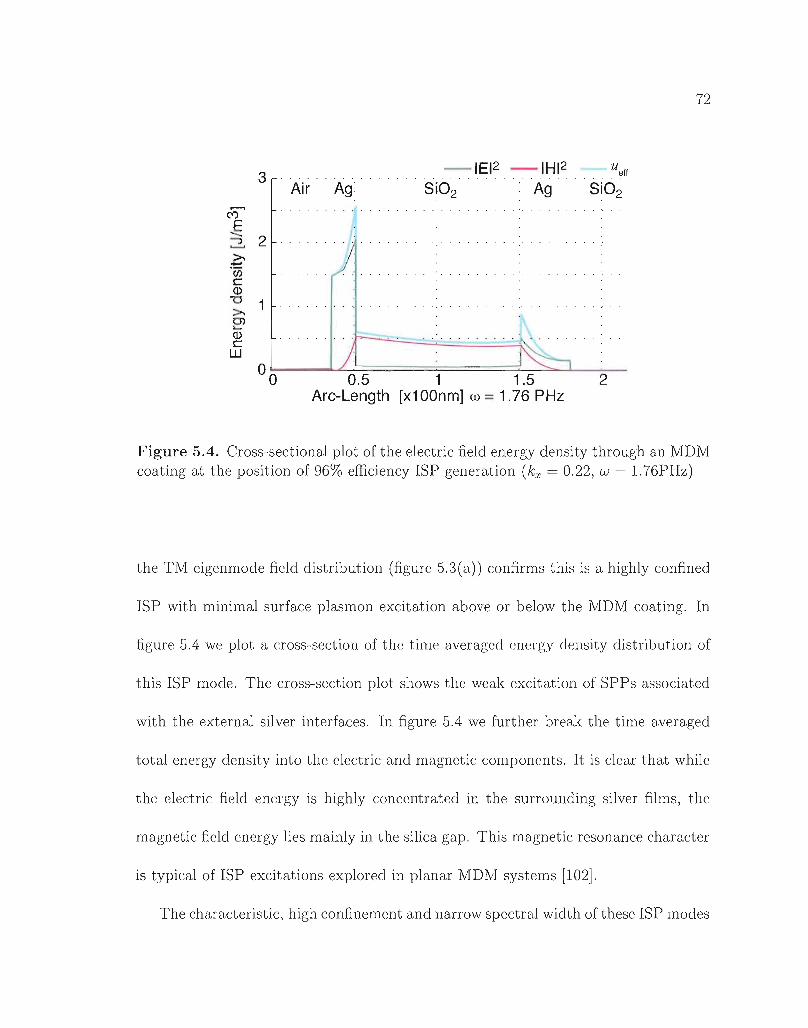
72
3-IEI2 -IHI2 ueH
Air Ag Si02 Ag Si02C0E-..
2:?.>.....
'00cQ)-0 1>.
' . ' ..
0>'-Q)cW
00 0.5 1 1.5 2Arc-Length [x100nm] w = 1.76 PHz
Figure 5.4. Cross-sectional plot of the electric field energy density through an MDMcoating at the position of 96% efficiency ISP generation (kx = 0.22, w = 1.76PHz)
the TM eigenmode field distribution (figure 5.3(a)) confirms this is a highly confined
ISP with minimal surface plasmon excitation above or below the MDM coating. In
figure 5.4 we plot a cross-section of the time averaged energy density distribution of
this ISP mode. The cross-section plot shows the weak excitation of SPPs associated
with the external silver interfaces. In figure 5.4 we further break the time averaged
total energy density into the electric and magnetic components. It is clear that while
the electric fidd energy is highly concentrated in the surrounding silver films, the
magnetic field energy lies mainly in the silica gap. This magnetic resonance character
is typical of ISP excitations explored in planar MDM systems [102].
The characteristic, high confinement and narrow spectral width of these ISP modes

73
makes them a useful candidate for future applications in nanoscale device fabrication.
The maximum field energy density generated in the silica gap by the excited ISP mode
(Ugap r-v 0.5 J/m 3 ) is enhanced by three orders of magnitude over the average energy
density of the incident W = 1.76 PHz plane-wave (upw = 0.0056 J/m 3 ). This could
prove very useful for applications in which large field enhancements in nano-scale
volumes playa critical role such as SERS [52]. Additionally the narrow resonance of
the ISP mode creates the opportunity for high sensitivity sensors. As an example,
in figure 5.5, we plot the change in the ISP central resonance frequency, We as a
function of interior dielectric constant nd. We see that a change of refractive index
of r-v 1% is sufficient to shift We by its full width half maximum. This corresponds to
NI 1829::.'
8, 1.80
Gc~ 1.78rr~
LL 1.76Q)olij 1.74ca(/)&1.72
~C 1.70Q)
o
II
11I
I
•••••••1•••••••••••••••II
I1............... ·1······111
IIII
0.97 0.98 0.99 1.00
nIno
1.01 1.02 103
Figure 5.5. Change in central resonance frequency of kx- = 0.22 ISP resonance as afunction of D.n = nino, where no = 1.42. Error bars indicate the resonance full widthhalf maximum (F\iVHM). A one percent change in the index of refraction is sufficientto shift the central frequency by the resonance FWHM.

74
6.w/6.n = 2PHz per refractive index unit or 1.2t.tm/RIu. This is two times the value
of the state of the art grating based SPR sensors. For comparison, the best value for
grating based surface plasmon biosensors is given by Homola et al. as 0.63t.tm/RIU [16].
ISP Control of SPP Enhanced Transmission
It has been shown that periodic modulation of a metal film leads to enhanced
transmission through the metal due to the excitation of SPPs on both sides of the film
(d. [19,103] and references therein). To compare the transmission through an MDM
to this SPP enhanced transmission, we have simulated the transmission through a
modified MDM coating with the top silver layer removed (a DM coating). This creates
a symmetric (silica-silver-silica) system capable of SPP enhanced transmission. In
figure 5.6 we show the transmission through the modulated DM and MDM coatings.
As can be seen in figure 5.6(b) the enhanced transmission through the the DM coating
is very broad, and exists in the regions between the branching modes of the air
and substrate SPPs. In contrast, the transmission through the MDM structure,
figure 5.6(a), is tightly bound to the excitation of the ISP modes. The maximum
transmittance through the MDM structure is comparable in magnitude to the DM
structure, but now its angular emission characteristics have been shaped by the ISP
mode dispersion.
To gain insight into this ISP transmission masking we examine the energy density

75
MOM Transmi sian OM ransmissian0.2 0.3 04 0.5 0.6 0.1 0,2 0.3 04 0.5 0.6
0.50.5
0.5 00.5o
.........,NI'-'
8>. >.u uc c0) 0):::Jc- c-O) 0)lo- l0-
LL LL
1 1
Figure 5.6. Transmission through (a) the MDM silver-silica-silver of figure 5.2 and(b) silica-silver (DM) coating coating created by removing the top silver layer fromthe geometry shown in figure 5.2.

76
distributions created from an incident plane-wave around the MDM enhanced trans-
mission point (k:c = 0.23,w = 2.67PHz). In figure 5.7 energy density cross-sections
at varied incident angles around the maximum transmission angle of kx = 0.23 = 11 0
are plotted. This shows that maximum transmission does not happen at the loca-
tion of most efficient ISP generation (kx = 0.19), but rather when the ISP is most
efficiently coupled to the symmetric SPP mode of the silver-silica interface. 'When
this condition is met, the electromagnetic field is strongest exiting the IVIDM film
and maximum transmission is found. When the ISP does not generate the strong
symmetric bottom film SPP, enhanced transmission is prohibited.
kx =0.48
Si02 :
----------------------------- .. ----------------
... :
-kx=O -kx =0.19 -kx =0.23
Air Ag :Si02 AgC0' 0.6E
:::::> 0.5~
>.'175 0.4c.gj 0.3>.2' 0.2Q)
tf} 0.1
0 0 0.5 1 1.5 2 2.5Arc-Length [x100nm] w = 2.67 PHz
Figure 5.7. Cross-sectional plots of the electric field energy density through anMDM coating for varied incident angles around ISP enhanced transmission maxima(kx = 0.23, w = 2.67PHz).

77
Coupling of ISPs to Localized Cusp Modes
We end this discussion of ISP mode coupling with the an examination of the
ISP coupling to the last dominant mode type mentioned in the introduction: the
cusp localized surface plasmon mode. The intersection of two cylinders or shells
creates nano-scale points (or cusps). In this simulation the cusps are formed by
rounding off the geometric points formed at the intersections of the layers and rods
with the artificial computation boundaries. This is done with radius=2.5nm spheres.
Cusp modes are characterized by very large ("" 102) field enhancements and flat
dispersion [104, 105]. By changing the periodicity (that is, the cylinder radius) of
our MDM structure to 300nm we show the development of such a nearly flat band at
w = 3.2PHz, (figure 5.8). We have additionally shrunk the dielectric spacer thickness
to 60 nm to maintain the high confinement condition Ao/10, as above.
In figure 5.8 we plot the dispersion relation and normal absorption of a 300nm
silica cylinder with a 30nm-60nm-15nm silver-silica-silver MDM coating. Again, the
dispersion relation is overlaid upon the film absorbance. As above, the absorbance
was calculated by simulating a plane-wave incident from the air side of the MDM
with wave-vector k = ko(sin ex + cos ey). At w = 3.2 PHz a flat band extends from
kx = 0 to kx = 0.34. At kx = 0.34 interaction with other modes reduces the excitation
of the LSP. The mode structures of the localized mode at kx = 0 and the hybridized
LSP/ISP/ESP mode formed at k = 0.40 are shown in figure 5.8(b). In figure 5.8(a)

78
Absorbance Hz, E Field Plots
2000
1500I
N
-+1000 ~
500 ~
0
-500
~ •• , I I , , , I
U •• I I I , I , , , ~
4c .. I , t I , I I I ; ,
<D \ , t I , I J J , ...
:::J ... \ \ , I I I I I , ,
0"' ,\\Itlll,2\ I I I I I ...<D f ~ 1/ ...Lt2 ~// I- /.,-0 N
~-2 3
~
-4- ....
-61
0 kx 0.5 .. 300nm -.Figure 5.8. (left) Band diagram overlaid upon normal absorption of a a = 300nmMDM coating. This geometry supports a localized, dispersionless plasmon cusp modenear w = 3.37PHz (560nm). (right) Magnetic and Electric field distributions of (a)the localized cusp mode at (kx = 0, Wk = 3.37PHz) and (b) the LSP /EPS/ISP hybridmode at (kx = 0.40, W = 3.3 PHz). The filled contour plot is the Hz magnitude, andthe arrows are proportional to E = Ex,i + Eyt;.

79
we plot the Hz and E fields of the cusp mode. In addition to the significantly small
field volume, it shows the large (rv 103) enhancements of the cusp mode Hz amplitude
with respect to the hybridized mode of figure 5.8(b).
Conclusions
Using FEM calculations we have demonstrated that it is possible to directly couple
freely propagating modes to ISP (gap plasmon polaritons) using the grating coupling
method. Narrow resonance (6:.w/w = 0.02) and high coupling efficiency (96%) is
possible under tunable excitation conditions. This can be done even with very thin
(15 and 30nm) silver films, providing very low absorption loss while maintaining high
spatial confinement (,\/10). We have additionally shown the effect of the existence
of the interior plasmon mode on the surface plasmon enhanced transmission. The
interior plasmon mode can be use to tailor the enhanced transmission characteristics of
the modulated metal film with minimal impact on the overall transmission efficiency.
Lastly the plane-wave excitation of localized cusp modes has been demonstrated and
we have shown the large field enhancements associated with the excitation.

80
CRAPTER VI
FABRICATION OF PERIODIC MDM COATINGS
Introduction
In this chapter we manufacture and analyze a novel 2D plasmonic surface which
is to be used in studying coupled ISP excitations in open Bragg resonators. Using
evaporative self-assembly we deposit monolayers of hexagonal close packed (RCP)
silica spheres to act as a hemispherically modulated substrate for conformally coated
silver-polystyrene-silver MDM trilayers. We use surface analytical tools such as scan
ning electron microscopy and atomic force microscopy to characterize the quality of
the prepared samples.
Monodisperse Silica Spheres
A crucial ingredient in creating RCP silica sphere monolayers (also referred to
as monolayer opals) is the synthesis of monodisperse silica spheres with radii in the
200-500nm range. We accomplish this using the well published Stober method [106].
In our work, the Stober reaction is the hydrolysis of tetraethylorthosilicate (TEOS) in
ethanol. In a base-catalyzed environment, nucleation of silica nanoparticles grow to

81
form monodisperse ensembles of micron-scale spheres. The standard deviation of the
sphere size is the most important parameter in growing high quality ordered crystals.
Thus, following the work of Gieche [107, 108], we have grown batches of silica spheres
based on the recipes shown in table 6.1.
Chemical Reaction Method
All glassware was pre-cleaned with hydrofluoric acid and subsequently dried at
800 for at least 6 hours before use. This prevented contamination by parasitic water
and dust particles; the former is a reactant and the latter facilitates uncontrolled
nucleation of silica particles. Random nucleation destroys the monodispersity of the
silica sphere ensemble, and thus must be avoided. Typical 200ml reactions were
prepared by combing all reactants except the TEOS in 500ml round bottom flasks
under vigorous stirring. TEOS was distilled at 1650 just prior to use and mixed 1: 1
with ethanol (EtOH) before rapid injection into the round bottom flask. The most
monodisperse reactions were obtained when the TEOSjEtOH mixture was quickly
Table 6.1. Stober reaction constituent molarities for synthesizing monodispersesilica spheres in ethanol. The resulting sphere average diameters and standard deviations are also given. (y indicates active cooling.
S-Rxn TEOS H2O NH40H EtOH (mL) Temp (DC) R (JR
3 0.2 13 4.2 70 30T 235 15.65 0.18 13 4.2 140 20 285 12.46 0.1 13 4.2 144 lOt 250 13.58 0.18 13 4.2 140 20t 200 9.59 0.18 13 4.2 133 20 250 9.610 0.2 13 4.2 128 20 258 10.2

82
50
100
o
S-Rxn 5250 <R> =285 nm
OR = 12.4
PO =4.3%200
Radius (nm)
(f)
C:Jo 150U
(a)
Figure 6.1. (a) Measured size distribution and (b) SEM image of Stober reaction 5.
and smoothly added below the solution surface with two extra-long wide-bore needles
on 5ml syringes. The reactions were allowed to proceed for at least 6 hours before
centrifugation cleaning in EtOH. The resulting monodisperse spheres were stored in
EtOH until needed for deposition.
Sphere Distribution Characterization
Small amounts of the Stober spheres were dispersed on copper-Formvar transmis-
sion electron microscope (TEM) grids for sizing with our Hugh transform analysis
algorithm [109]. Sizing results for the spheres used in this work can be found in
figures 6.1 and 6.2. A summary of batch polydispersities (= O"R/ < R » can be
found in table 6.1. Despite contrary reports [110], it was found that post growth

83
(a)
100
80CI)c:;8 60
40
20
S-Rxn 9<R> = 250 nm
OR =9.6PD = 3.8%
200 210 220 230 240 250 260 270 280
Radius (nm)
Figure 6.2. (a) Measured size distribution and (b) TEM image of Stober reaction9.
sedimentation filtering had minimal impact on the overall sphere size polydispersity.
This is most likely due to the fact that a seeded growth process was not used to
initialize the Stober reaction. This results in a monodisperse distribution of sphere
diameters rather than a bimodal distribution, making sedimentation filtering much
less effective. Using the above procedure, typical polydispersities of 4% were obtained
with deviations between 3% and 5%.
This was deemed acceptable for Hep crystallization, as polydispersities below 6%
have been shown to produce high quality ordered crystal structures [111]. Despite
this, it should be noted that smaller polydispersities result in opal monolayers with
fewer point and line defects. Wong, et a1. have shown that very large (> 104,um2)
single domains are possible if the sphere polydispersity < 2% [110].

84
Air CurrentIsolation
Chamber
Vibration Isolation(b)
Figure 6.3. Diagrams of (a) evaporative self-assembly process and (b) theisothermal-heating evaporative self-assembly (IHESA) chamber built to grow vertically deposited opal monolayers. (c) A picture of the IHESA chamber, before theaddition of the evaporation filtration pump.
Isothermal Monolayer Self-Assembly
The crystal growth process is conducted with vertical deposition evaporative self-
assembly. Illustrated in figure 6.3, evaporative self-assembly works through the
surface-tension aided deposition of colloidal particles at the meniscus of an evapo-
rating solvent. This process is notoriously susceptible to environmental conditions
and can result in enormous variability in the quality of the crystals produced.
To overcome these difficulties, we follow the work of Wong, et al. in engineering
a crystal-growth chamber (figure 6.3) to uniformly deposit ordered monolayers over
large areas with high reliability and repeatability. The control of the crystal growth

85
process is based on isothermal heating, evaporative self-assembly (IHESA). The IH
ESA method relies on the immersion of the solvent-particle (EtOH-silica sphere)
slurry into a strictly controlled temperature bath. By maintaining the heat bath at a
temperature slightly above the boiling point of the evaporating solvent, uniform con
vection of the evaporating solvent stirs the slurry without disturbing the deposition
meniscus. The convective flow ensures a constant uniform concentration of spheres
at the meniscus during the deposition process. In addition to the approach outlined
in [110], we have added the continuous, constant removal of the evaporating solvent
vapor (KNF Lab N811KV Filter Pump) and total isolation from external air currents.
This has improved the repeatability of the deposition process by eliminating solvent
re-condensation within the evaporation chamber. The isothermal bath chamber is
machined from a solid block of polyethylene and filled with rv 1 liter of ethylene gly
col. The temperature of the bath is maintained by a NESLAB RTE 111 circulating
temperature controller, and monitored with a platinum resistance thermometer. The
heat of the circulating fluid is transfered to the ethylene glycol through copper tub
bing inside the iso-bath chamber. Vye have found that this setup reliably produces
large area synthetic opals with a tunable number of layers for of sphere sizes in the
range r = 200 nm - r = 380 nm.
The concentrations of silica spheres used to create a sphere monolayer were estab
lished by starting with a high concentration of sphere (> 2% by weight) and succes
sively halving the concentration until a monolayer was obtained. Typical deposition

86
concentrations can found in table 6.2. It should be noted that the temperature of the
evaporating solvent must be controlled to a very high tolerance during the deposition
(±0.05° typical). Additionally, the temperature of the IHSEA isothermal bath must
be slightly above the boiling point of the solvent (cf. table 6.2). It was found that the
most critical parameter for successful deposition is the temperature of the evaporating
solvent. The solution temperature must be at (or slightly above) the solvent boiling
point. In our depositions, we found that a solvent temperature of 78.9 ± 0.5° was
adequate for successful ordered growth. The temperature of the evaporating solvent
will change as a function of the surface area exposed to atmosphere. As a result,
careful control experiments were conducted to establish the correct isothermal bath
temperature for situations where the deposition vial geometry was changed.
When used as evaporation vessels, large (25ml) scintillation vials with an aspect
ratio of 3: 1 (length:width) were eventually found to produce the best results. The large
volume of these containers ensured a large reservoir of sphere solution and provided
a nearly constant concentration of spheres during deposition. The deposition vials (
Table 6.2. Typical deposition parameters for crystallization of opal monolayers.Vacuum levels were held at 6.25" Hg for all reactions, and "S Rxn" cross-referencesthe table 6.1 reaction numbers. The deposition time is given in hr:mins.
Sample Chiller (OC) Iso-Bath (OC) Radius (nm) S Rxn % weight Time57 86.45 84.03 285 5 2.6 3:2060 86.35 84.05 285 5 2.6 2:5584 86.35 83.90 250 9 0.3 -
86 86.35 83.92 250 9 0.3 3:0087 86.35 83.73 300 8 0.67 3:00

87
(a) (b) (c) (d) (e)
Figure 6.4. Examples of silver coated opal monolayers with a variety of sphere radii:(a) 200nm (b) 250nm (c) 285nm (d) 250nm (e) 285nm. The glass substrates arecut to 5/8" x 3/4". Second layer striping manifests as darker regions and speckle.
and the cut 3/4" x 3" microscope slides on which the deposition takes place) were
pre-cleaned with fresh piranha (3:1 fhS04 : H 20 2 ) solution for at least one-half
hour before deposition. After cleaning, the slides and vial were rinsed with ultra-
pure water and then rinsed with copious amounts of EtOH. In addition to removing
the residue and dust disruptive to the crystallization, it is important that no micro-
porous contaminants be in the vial during deposition. Because the temperature of
the solvent is so close to boiling, any air pockets or microscale sharp points can lead
to micro-heating. This causes the solution to boil and destroys the crystallization
process.
Cut microscope slides (Corning 2947) were cleaned and suspended in the evapo-
rating solvent with heated copper clamps (thermally attached to the isothermal bath)
to prevent solvent recondensation and dripping. Typical depositions took 3-3.5 hours,
indicating a linear evaporation rate of '" 1.5cm/hr. This most commonly resulted in

88
... ~ ,,"(Lt..)", '" / " . ,. .u ~ v~.. til .. Y ',. y ... '(
: : • .. y-J .' I ~.., ~ .. ,,".... ",,,., J" ,".,/0;'"j ~ ~ .. J ....;:,...... ~ I
A._I • 'f 't A " • .... .", . .,.• . ..
,• y
,• y
Figure 6.5. (a) An SEM images of silver coated opals taken at 5 kV. (a) showinga typical line defect across its length. Note that the dark spots are imaging artifactsdue to surface charging, and not crystal defects. (b) a high magnification image of atypical point defect from a small sphere. Both opals are coated with 50 nm of silver.
an evenly coated I" - 1.5" X 3/4" area of uniform ordered-monolayer deposition with
second layer striping on both sides of the microscope slide. Several examples of silver-
evaporated monolayer opals are shown in figure 6.4. The monolayer opals were then
carefully removed from one side of the slide by wiping with acetone and lens tissues.
The resulting single sided samples were then allowed to dry overnight before further
processmg.
lVIDM Layer Deposition
High Vacuum Silver Deposition
After drying, monolayer opals were coated with an optically thick silver layer using
high vacuum (HV) evaporation. A Key high vacuum metal evaporator was used to
deposit a 50nrn thick layer of silver at a slow deposition rate of 0.3 - 0.5,4/5. The

89
results of such a deposition can be seen in figure 6.5. A polystyrene polymer layer
is then applied and an additional top 20nm thick layer of silver is evaporated on top
of the monolayer opal, forming an MDM structure. In addition, one opal monolayer
was coated with 70nm of silver and no polystyrene interstitial layer, to be used as a
control sample.
Spin Coating of Polystyrene Conformal Layers
Following the results of Hall, et al. we have used high molecular weight polystyrene
(Alfa Aesar, #41936, MW:200,000) dissolved in toluene to conformally coat the
monolayer opals [112]. Huang, et al. have shown that spin coating can produce
thin (rv 100nm) conformal PMMA layers on a sinusoidally-modulated surface with
high (1:1) aspect ratios [113]. We have applied this same method to generate uniform
polystyrene layers of controlled thickness (from 120-160nm) over the surface of coated
opal substrates.
To calibrate the thickness of the polystyrene films, glass cover-slips were prepared
with piranha solution cleaning. One-half of the cover-slips were then coated with
50 nm of silver, using the same HV evaporation deposition as above. Following Hall,
et al. 4% by weight, polystyrene and toluene solutions were prepared and stirred
in a VWR vortex stirring machine for at least one-half hour before spin coating.
Calibration graphs for spin settings vs. layer thickness were then produced for speeds
between 2000 rpm and 6000 rpm. The samples were completely covered with the

90
230
220 • PS on Silver
210 • PS on SilicaExp Fit, Silver
E200 Exp Fit, Silica
5 190VI 180VIQJC 170~
.'::! 160J::I- 150
140
130
120
1102.5 3.0 3.5 4.0 4.5 5.0 5.5 6.0
Speed (krpm)
Figure 6.6. Calibration of spin coat rotation speed vs. polystyrene layer thickness.The layer thickness and standard deviation are shown for two substrates (silver andsilica) using 4% by weight polystyrene in toluene. Least squared fits to exponentialfunctions are also shown.
coating solution and then spun for 60 seconds and allowed to dry overnight. After
scoring the sample with a razor blade, a Dektak 6 surface profileI' was used to asses
the height and uniformity of the polystyrene film. Up to ten independent 5 /-I,m
long scans were taken for each sample, and used to plot the average thickness and
standard deviation of the film (see figure 6.6). Conformal polystyrene coatings were
then applied to silver-covered opal monolayers with spin conditions selected to create
polystyrene layers with thickness from 125nm to 160nm.

91
MDM Layer Characterization
The quality of the opal crystal domains and the uniformity of the polystyrene
and silver layers were assessed using scanning electron microscopy (SEM) and atomic
force microscopy (AFM). AFM images of silver coated and silver-polystyrene coated
mono-layered opals can be found in figure 6.7. These images demonstrate the re
tention of uniformly modulated hemispheric surfaces throughout the deposition pro
cess and spin-coating. The rv 5D nm reduction in the absolute magnitude of the
silver-polystyrene coated AFM image (as shown in figure 6.7(a)) indicates that the
polystyrene layer is preventing the AFM probe tip from penetrating as far into the
gaps between the spheres as its geometry allows. We surmise that polystyrene layer is
uniformly capping the silver coated opal. This is further confirmed below with SEM
images of MDM coatings
To assess the long range uniformity of the MDM layers and mono-layered opals,
SEM (Zeiss Ultra FEG) images were taken when conductive surfaces were available
(after silver evaporation). Figures 6.9(a) and (b) show the uniformity of opal mono
layers over long distances. In figure 6.8 we show detailed results of spin coating
an ordered monolayer with a layer of polystyrene. We note that, after polystyrene
coating, the defect locations of the monolayer opal are highly enhanced in the SEM
images. This is due to charging of the sample surface at the location of the holes in
the applied polystyrene layer. We have discovered that the polystyrene spin coating

92
117nm1.8
I0.2
1.8
0.2
(b)
-117nm
"'EL5L5LJE O[
.5 0.0>.
-0.[0.0 0.5 1.0 1.5 2.0
x {.JImJ
95nm1.80.2
1.8
0.2
(a)
--95nm
o,~~ 0.0
>'-O.I~qx [I'm]
Figure 6.7. AFM images of (a) silver-polystyrene, and (b) silver coated monolayeropals. Inset are line profiles of the highlighted paths in the above images.
process fails at the location of point defects (missing spheres) and line defects (crys-
tals domain boundaries) but is otherwise uniformly applied over large areas of the
monolayer opal.
The sensitivity of SPPs to surface features makes the high defect density a point of
concern. However, we will show in the next chapter that these defects do not eliminate
the signature of MDM ISP excitation. Further refinement of the sample growth
process should lead to improvements in crystal quality and domain size. Specifically,
the reduction in the polydispersity of the monodisperse silica spheres, either through
seeded growth [107] and/or more refined sedimentation filtration: would seem to be
the most important factor [110].

93
(b)
)
MJO nm-Figure 6.8. SEM images of silver-polystyrene-silver coated opal monolayers. (a) AnMDM layer near an open area in the HCP monolayer, with the red arrow indicatingthe crystal growth direction. (b) High magnification image of a break in the MDMlayer caused by an underlying line defect terminating in a missing sphere point defect.(b) also shows the suspended nature of the polystyrene layer over the silver coatedopal. The polystyrene does not fill t.he interstitial voids of the crystal monolayer.
(al
ium-
(bl
Figure 6.9. SEM images of the long range order of the HCP monolayers. Silverpolystyrene-silver coatings are shown capping the opal monolayer. The polystyrenelayer is seen to fail at defect sites in the underlying crystal.

94
The use of more advanced methods for deposition of the dielectric spacer (chemical
vapor deposition or pulsed laser ablation deposition) may produce better results for
thinner layers. However, we find that, away from the crystal defect areas, spin coating
of '" lOOnm thick polystyrene layers proves to produce adequate conformal layers
suitable for creating plasmonic MDM layers.

95
CHAPTER VII
ANGLE RESOLVED SPECTROSCOPY OF MDM COATINGS
Introduction
A defining quantity of SPPs are their unique dispersion relations. In chapters
II and III we have shown that MDM layers and shells can be used to tailor the
dispersion relation of plasmonic surfaces. In this chapter we design an experiment to
measure the dispersion characteristics of the periodic silver-polystyrene-silver trilayers
engineered in the previous chapter. By measuring the far-field transmission spectra
of our periodic MDM surfaces at a variety of incident angles we are able to trace out
their dispersion relations. Using this angle resolved (AR) scattering spectroscopy, we
will find evidence that the manufactured MDM substrates support ISP modes, and
that these modes alter the SPP enhanced transmission found in sub-wavelength hole
arrays. We will end this chapter with the observation of a new phenomenon, angularly
asymmetric SPP enhanced transmission through silver coated opal monolayers.

96
Design and Alignment of an Angle Resolved Spectrometer
AR Spectrometer Overview
To investigate AR transmission and reflection we have built a spectroscopy system
capable of independently altering the collection angle while automatically controlling
the incident angle and wavelength. The setup is shown schematically in figure 7.1.
The AR spectrometer has a 0.8° angular resolution, 111m spectral resolution and a
pointing accuracy of 40 J..lrad. By using high sensitivity detectors we can utilize a
collimated incandescent light source while maintaining reasonable acquisition times.
Acquisition speeds vary with sample extinction, but typical scan times for the samples
studied here are between two three hours with 2° and 2 nm resolution.
To produce a small sample area at the sample, light from an incandescent source
Fiber CoupledDetector
l'.NA eoutput out
ComputerControl
l'.NAinput
~
tFocusingLens L2
Lock-in Amplifier
Collimating 80/20 BSLens L1
Fiber coupledIncandescent
source
Monochrometel
Figure 7.1.. Schematic layout of angle resolved spectroscopy system.

97
is coupled to a 200l1m core diameter multimode optical fiber (Thorlabs M254L02)
with an aspheric fiber collimator (Thorlabs F220FC-B) optimized for the 600-1050 nm
range. This provides a pseudo-point source which can be directly coupled into a short
focal length spectrometer (Acton Research SpectraPro 2300i). This provides us with
a tunable spectral source with 1 nm resolution. The use of a pseudo point source
at the entrance of the spectrometer allows us to create a highly collimated output
beam. We use an achromatic 100mm lens (L1) to collimate the output beam before
splitting it with a 20/80 non-polarizing beamsplitter. The 20% exit beam is directed
into a fiber-coupled, femtowatt photoreceiver (New Focus 2151). This measurement
is used for realtime normalization of the input signal. The beam is chopped at a
frequency of 650 Hz and the resulting output signal is recorded with a Stanford
Research lock-in amplifier (SR830). The remainder of the input beam is directed
to the sample (rv 1.5 m down-beam) passing through a Glan-Thompson polarizer
(Newport 10GT04AR.16) set to select p-polarized light with respect to the vertical
rotation plane of the sample (d. figure 7.3).
The collimated beam is focused onto the sample with a 250 mm achromatic lens.
The input beam NA is adjustable from 0.04 to 0.008. After the sample, the transmitted
reflected light is collected at a variable collection angle (manually adjusted) with a
combination achromatic lens (j = 75.6 mm) and fiber collimator (Thorlabs F220FC
B) system. The collection NA is adjustable with a calibrated iris between the collec-

98
ooo
Retractable Inspection Microscope~--- --- ----.
IOutput Fiber
Detector Swing Arm
nl
~X-y-/Wra",lallon
Manual Detector HotaHon Stage-~~~------~~~---~.
Figure 7.2. Detailed illustration of the angle resolved sample holder, the fibercoupled collection optics, and the sample inspection microscope.
tion lens and the fiber collimator. The NA is adjustable from 0.11 to 0.013 providing
a collection resolution range of 6° - 0.80.
The collected light is coupled into a 65 fJ,m multimode optical fiber (Thorlabs
M14L02). We have measured collection efficiencies equal to 65% at633 nm. The use
of a fiber coupled detector allows the detection angle to be varied from -300 to 1500
without beam realignment. The details of the sample and detector optomechanics can
be found in figure 7.2, and a detailed illustration of the sample coordinate systems can
be found in figure 7.3. The fiber collected light is then detected with a thermoelectri-
cally cooled photomultiplier tube (Hamamatsu 633) set at maximum gain (1500V).
The output of the PMT is digitized with a 20bit analog to digital converter (Acton
SpectraHub) and collected with our custom Labview acquisition software. The fem-

99
towatt photoreceiver normalization signal is simultaneously collected and recorded
using the SR830 internal data buffer. With the high sensitivity and large dynamic
range of the PMT detector and the 20bit converter we have established that our cur
rent spectroscopy setup has a noise equivalent power of 10-5 at 650 nm (in normalized
units) .
The sample stage consists of an automated rotation stage (Thorlabs CR-Z6)
mounted on linear x-y translation stage. The translation stage aligns the automated
rotation stage center of rotation with the manual rotation stage supporting the fiber
coupled detector. The sample automated stage and the spectrometer are also auto
mated and controlled with custom Labview software. This allows for the automatic
acquisition of spectrally resolved data from a sample, as the sample is rotated about a
fixed point in space. As the input beam is held fixed, the sample rotation is equivalent
to changing the incident angle. In this study, the detector fixed at ()out = 00• Thus,
as we rotate the sample we record the zero-order extinction of our MDM coated opal
monolayers.
Center of Rotation Alignment
The AR spectroscopy system has two alignment tools incorporated into its design:
a common path ReNe laser and a home built, retractible, 60x inspection microscope.
\iVe use the ReNe laser to mark the sample stage center of rotation and to select
highly ordered sample locations. When centered on a highly ordered location the
crystal structure of the substrate results in well defined diffraction with characteristic

100
6 fold symmetry. The alignment microscope is used to inspect the sample surface, set
its z-axis position to the focal plane of the lens L2, and to initially align the sample
stage center of rotation (see figure 7.2) .
The primary alignment task needed in the AR system is locating the sample stage
center of rotation in the x- i plane. This is accomplished by first placing a thin film
40 p,m pinhole in the sample holder. Next, the pinhole is translated to the stage center
of rotation by iteratively imaging it with the alignment microscope at the 0° and 180°
stage positions until the two locations overlap at the center of the microscope field
of view. This can be accomplished with a replacement accuracy of approximately
±5 p,m. The small depth of field of the 60x objective « 1p,m) further aligns the
pinhole location along the i-axis with the sample stage center of rotation.
The fiber coupled detector is aligned by reversed coupling of the ReNe laser back
wards through the collection optics. Independent x- i linear translation stages are
used to align the pine-hole marked center of rotation of the sample stage with the
focused laser beam emanating from the collection optics. This procedure aligns the
center of rotation of the detector with the center of rotation of the independent dove
tail swing arm supporting the collection optics.
With the location of the sample stage center of rotation established, the ReNe
alignment laser is focused on the the location of the pine hole with the manipulation
of L2 along i and with an independent linear translation stage along x. Additionally,
the laser beam passes through a fixed beam pick-off optic after the focusing lens. The

101
sampled beam is used to align a fixed pinhole, now matched to mark the center of
rotation of the sample stage in 3-dimensions. Subsequent alignment of the samples can
now be accomplished by illumination with the HeN'e alignment laser (x, y, e= 0, ¢ =
0) and bringing the sample surface into the focal plane of the alignment microscope
(2).
AR Spectrometer Calibration
Chromatic Correction
To overcome the inherent variabili ty of our incandescent light source on the time
scale of an AR scan (rv 2 hours) we have incorporated the real time signal normal-
ization mentioned above. Because the two detectors used ar<~ not identical, we must
Incident l ! !cp t t tT L S
x(a) Crystal Sample (b)
Figure 7.3. (a) Coordinate system of an oriented sample in the AR spectrometer. (b)Geometry of a periodic .\IIDM based on a self-assembled monolayer of silica spheres.Blue is silica, gray is silver, and yellow is polystyrene. The system is embedded inair.

102
1.2_--_---__---.....--__.---......---....---__._--_
Input Spectrum -Chromatic Normlization Spectrum -Corrected, Normalized Spectrum --
::J
<Ii
CQ)
~:JUo....o.c0...-0Q)
.~
CO§oZ
550 600 650 700 750
Wavelength [nm]800 850 900
Figure 7.4. Normalization of input signal, and chromatic correction for non-identicaldetectors. The resulting signal has a noise level of less than 0.005 at 650 nm.
account for their individual spectral responsivities. We do this by collecting spectra
without a sample in place. Division of the signal with this bright-field correction cal-
ibrates the chromatic differences between the P:VIT and the femtowatt photoreceiver.
Such a chromatic correction spectrum can be seen in figure 7.4, along with a raw
input spectrum and the resulting normalized signal.
AR Spectrometer Validation
Before beginning our discussion of zero-order AR transmission through periodic
MDM coatings) we discuss several test cases. These are used to check the performance
and alignment of the spectroscopy system. In figure 7.5(left) we plot the transmission
through a 50 nm thick high-vacuum-deposited silver film. The plotted result demon-

103
71'1< I 71'1.1
80
1.5
(,()
1.0
40
n.520
0.0 0
Figure 7.5. (left) Zero-order AR transmission through a flat 50nm thick silver film.(right) Zero-order AR transmission through uncoated opal 83 « R > = 285 nm).
strates the symmetry of the AR collection about the rotation origin of zero degrees
(normal incidence). As shown in figure 7.3, negative and positive rotations respec-
tively correspond to clockwise and counter-clockwise rotation of the sample stage.
We can also see the low (T "" 1.9%) transmission through this 50 nm think film.
Below we will see, that the periodic lVIDlVI and DlVI structures we have manufactured
in the previous chapter exhibit transmission enhancements on the order of 10 - 20
at 750 nm. The ripple structure in figure 7.5(left) is a result of noise from the low
input intensities at the ends of our collection spectrum ("" 480 nm and 900 nm) and
the high extinction of the flat film. The large variation in the noise level is due to the
large variation of the input spectrum (d. figure 7.4).
The left hand side of figure 7.5 shows the AR, zero-order transmission through an
uncoated opal monolayer self-assembled from r = 285 nm silica spheres. The figure

104
TI',i125
20
15
10
5
o
Figure 7.6. (left) Zero-order AR transmission through a polystyrene and silvercoated monolayer opal 83 (L = 100 nm, T = 20 nm), (right) overlaid with the anomalous diffraction from the air-silver interface (green line).
shows the same rotational symmetry of the transmitted light as seen in the flat film
case. A weak diffraction dip can also be seen centered at "'-J 2.8 PHz. This is the result
of a highly ordered monolayer, and proves that we can use our system to investigate
the angle resolved scattering from structures built from our self-assembled crystals.
In figure 7.6 we plot the collected zero-order transmission from an opal with a
polystyrene and silver coating. The polystyrene coating is "'-J 100 nm thick, and ap-
plied with the spin coating method discussed in chapter VI. The coating was spun
from a 3% by weight, polystyrene-toluene solution at 5.2 krpm for 60s arriving at the
estimated 100nm thick coating [112]. A 20nm thick silver film was then evaporated
on top of the polystyrene layer, under high vacuum. The results, plotted in figure 7.6,
have one dominant feature. The symmetric "X" centered at 3.3 PHz (570 nm). This
extinction feature is due to anomalous diffraction from the periodic, 2D, silver grat-

105
ing we have created. This so called, anomalous diffraction, occurs when a diffraction
order (the first order in this case) reaches the grazing output angle of 900 [114]. This
condition can be approximated from the grating equation, as the solution of:
. e nout AoSIn in = -- - m--
nin ninam=(1,2,3, ... ) (VII.l)
where ein is the input angle, nin (nout) is the refractive index on the input (output)
side of the grating, Ao is the free space wave length, and a = 570 nm is the first order
periodicity of the grating (equal to the sphere diameter in this case). In the right-
hand side of figure 7.6 we have potted the overlapping solution to equation (VII.l) on
top of the transmitted spectra's extinction dip. Despite the crude approximation of
the simple grating equation, it is obvious that the solution of (VII. 1) coincides with
the extinction dip, identifying it as anomalous diffraction.
Scattering from Silver Coated Opal Monolayers
VVe begin our discussion of MDM coated opal monolayers by first looking at the
normal (ein = 00) transmission through a silver coated opal monolayer (5 = 70 nm).
The zero-order (eout = 00) transmission for such a sample is shown in figure 7.7. As
compared to the data taken from a 50 nm thick high vacuum evaporated silver film,
there is a large transmission enhancement at 750 nm. From the spectral shape of the
transmission, its spectral location of 750 nm, and the lack of a similar feature in the
normal transmission through an uncoated opal monolayer (also plotted in figure 7.7)

106
Uncoated Opal 86 x1/850nm Flat Silver Film
70nm Silver Film on Opal 57b •
...._-~~..-
.....
600 650 700 750
Wavelength (nm)550500
C 0.120
'(j)0,1.!!?
ECJ) 0,08CCO~
f- 0.06"0Q)
.~ 0,04
COE 0.02...0Z
0 450
Figure 7.7. SPP enhanced zero-order transmission at 750 nm (2.51 PEz) from asilver coated (5 = 70 nm) opal monolayer as described in the text. This is comparedto an uncoated opal monolayer, and the transmission through a fiat,50 nm thick, silverfilm. All spectra were taken with our AR spectrometer at normal incidence.
we conclude that this enhancement is the SPP enhanced transmission also found in
subwavelength nano-hole arrays [19].
The existence of SPP enhanced transmission is a very reassuring sign that our
manufacturing process supports the delocalized SPP modes. Enhanced transmission
depends on the long range structure of a periodic array to coherently couple SPPs to
radiating modes on both sides of the metal film. Our observation of enhanced trans-
mission implies that our self-assembled monolayers are of sufficient ordered quality to
support the coupling of the delocalized SPPs needed to generate SPP enhanced trans-
mission through the subwavelength holes formed from the gaps between the spheres
of the close-packed monolayer.
In figure 7.8, we present the AR, zero-order transmission from this silver coated

107
TI'hl
14
12
10
8
I)
4
2
()
Figure 7.8. (left) AR zero-order transmission of opal 57B. A S = 70 nm silver coatedopal. (right) The zero-order transmission with anomalous diffraction (green) and [01] silver-silica grating SPP dispersion (red) overlays.
opal monolayer. This figure shows the broad SPP enhanced transmission centered at
2.5 PHz (750 nm). In the right hand panel of figure 7.8 have plotted the same anoma-
lous diffraction resonance as above. This accounts for the dark bands in the center
of the transmission spectrum. In addition, we have plotted the first order disper-
sion band for a grating coupled SPP. As discussed in chapter II, the grating coupling
method yields the following coupling condition for exciting SPPs on a hexagonal
lattice (equation (II.7)):
with kll = ndkO sin ein, nd = JEd is the index of refraction for the particular (air
nd = 1, silica nd = 1.45, or polystyrene, nd = 1.59) dielectric medium adjacent to the
metal surface, Gf'K = 41r /3a and Gf'M = 21r / V3a. The band plotted in figure 7.8(b)

108
is the first order (m2 = 1) dispersion for the [0 1] ( GrM ) silver-silica SPP mode. As
shown in figure 2.4, vertically-deposited, self-assembled crystals grow along the [1 1]
real-space direction. Thus, as we rotate the crystal about the growth direction axis,
i) by an angle ein , we span the r~M high symmetry reciprocal lattice vector, GrM . In
figure 7.8(b) we see that the SPP enhanced transmission is broadly correlated with
the r-M SPP band associated with the silver-silica interface plotted with the filled
red circles. One may also observe that there is a strong asymmetry in the collected
data with respect to the normal incidence (ein=O) mirror symmetry axis. This will
be addressed in a later section.

109
NIDM Coated Opal Monolayers
Having established that our crystal monolayers are of sufficient quality to support
the grating coupling to SPPs, we now examine the effect of adding YIDM layers to
the surface of the ordered monolayer. Using the method discussed in chapter VI, we
have created several MDM coatings with a variety of dielectric layer thicknesses. The
details of the sample preparation can be found in table 7.1. The MDM layers have
thickness of 125 nm, 140 nm, and 160 nm.
On the left hand side of figures 7.9, 7.10, and 7.11 we have plotted the zero-order
AR transmission through the three MDM films. In tlw right hand panels we have
'TI'A I
2.5
2.0
15
1.0
0.5
0.0
Figure 7.9. (left) AR zero-order transmission of opal 57A. An ":VIDrvI coated opal withL = 140 nm. Red arrows indicate ISP extinction. (right) The zero-order transmissionwith [0 1] and [0 2] grating SPP dispersion bands for a silver-silica (red) and a silverpolystyrene interface (blue). The silver-air anomalous diffraction is plotted with greendots.

110
'T I'l.l
.\.0
1.~
2.0
I.S
1.0
o.s
0.1)
Figure 7.10. (left) AR zero-order transmission of opal 60. An MOM coated opal withL = 160 nm. Red arrows indicate ISP extinction. (right) The zero-order transmissionwith [0 1] and [0 2] grating SPP dispersion bands for a silver-silica (red) and a silverpolystyrene interface (blue).
overlaid the first [0 1] and second order [0 2] dispersion bands for the silver-silica
and silver-polystyrene interfaces. The ISP modes so heavily discussed in previous
chapters roughly correspond to the excitation of SPPs on the polystyrene side of
a periodically modulated silver-polystyrene film. From our work on MOM coated
cylinders in chapter V, we know that a major efFect found in our FEM simulations
was the alteration of the SPP enhanced transmission due to the prerequisite excitation
of ISP modes. Keeping this in mind, we note three features that suggest the excitation
of ISP modes in figures 7.9, 7.10, and 7.11 .
The most obvious change from the single silver coating of figure 7.8 is the shift
in the distribution of SPP enhanced transmission to include a broad branch centered
at (w = 3.7 PHz (510 nm), kx = 0). The over-plots of the [0 2] dispersion bands

III
Figure 7.11. (left) AR zero-order transmission of opal 64. An rvlDM coated opal withL = 125 nm. Red arrows indicate ISP extinction. (right) The zero-order transmissionwith [0 1] and [02] grating SPP dispersion bands for a silver-silica (red) and a silverpolystyrene interface (blue).
imply that this is due to the excitation of a second order ISP mode (the dotted blue
line). This silver-polystyrene interface mode exists neither in figure 7.8, when there
is no polystyrene layer, nor in figure 7.6, when there is only a single silver interface.
We therefore conclude that the broad SPP enhanced transmission found centered at
(w = 3.7 PHz, kx = 0) in all three MDM layers is due to the excitation of ISP modes
in the polystyrene gap between the two silver films.
A second characteristic change, induced by the application of the second metal
interface of the fvIDM coating, is the slight (but consistent) red-shift of the original
SPP enhanced transmission centered at (w = 2.5 PHz, kx = 0). In figure 7.8 it is clear
that this enhanced transmission overlaps with the first order [0 1] dispersion band
of the silver-silica interface. In all of the YIDM coated samples we see that the new

112
maximum of the SPP enhanced transmission has been red-shifted towards the first
order silver-polystyrene [0 1] dispersion band. This is consistent with our simulations
of chapter V. In those results, we found that the overlap of ISP bands with the SPP
enhanced transmission redirected the transmission along (but blue shifted from) the
ISP dispersion bands.
Finally, in figures 7.9, 7.10 (and weakly in figure 7.11) we note that, in addition
to the apparent shifting of the SPP enhanced transmission, we see the increased
extinction of the transmitted light corresponding to the [0 1] and [0 2] dispersion
bands. (These are marked with red arrows.) Because of the strong correlation between
the dispersion bands and the increased extinction, we conclude that they correspond
to the excitation of ISP modes which are absorbing/scattering additional light out
of beam. This is the most obvious in figure 7.9 with L = 140nm and figure 7.10
with L = 160 nm becomes less pronounced in the thin dielectric spacer layer with
L = 125 nm (figure 7.11). This suggests a change in the dispersion relation of the
Table 7.1. Geometry of opals presented in this study. The thicknesses L are esti-mates based on the calibration curve in figure 6.6.
Opal # < R > (nm) S (nm) L (nm) T (nm) % w.t. PS Spin (krpm)57A 285 50 140 20 4 057B 285 7060 285 50 160 20 4 3.0564 285 50 125 20 4 4.5584 250 30 100 20 3 5.2386 250 30

113
ISP with the dielectric layer thickness, and strong coherent coupling between the two
metal interfaces.
Asymmetric Transmission
We now move onto a newly observed phenomenon. We have found, that for some
silver-coated, self-assembled monolayers, the SPP enhanced transmission is asymmet
ric with respect to the mirror plane defined by the plane of normal incidence (ein = 0).
This was noted earlier in reference to figure 7.8. To test that this observation is an
inherent property of our sampIes (and not an artifact of our AR spectroscopy system)
we have measured the zero-order transmission with the sample in its original orien
tation (c/J = 0) and with the sample rotated 1800 about the surface normal axis (d.
figure 7.3). This was done for two independent points on the sample, and with two
different samples noted to have asymmetric SPP enhanced transmission. The results
can be seen in figures 7.12 and 7.13.
In figures 7.12(a) and (b) we have plotted the asymmetric transmission of the pre
viously examined silver coated opal from figure 7.8. The mirror symmetry between
the ¢ = 0 and ¢ = 1800 in figures 7.12(a) and (b) is obvious when plotted they are
plotted side-by-side. The mirrored SPP enhanced transmission happens, while the
anomalous diffraction band remains symmetric. We conclude that the sample has
inherent asymmetric transmission and that it is not a artifact of the measurement

114
Figure 7.12. Asymmetric zero-order transmission from silver coated opal 57B. (left)¢ = 0°, (right) ¢ = 180°. Both graphs are plotted on the same scale as figure 7.8.
process. The points measured were selected based on the visibility of their diffraction
patterns with the alignment BeNe laser, but were otherwise independent. The selec-
tion of two independent points for these measurements proves the robustness of the
observed asymmetric transmission. It implies that our samples are highly uniform
and that the cause of the asymmetry likely originates from some systematic, global
variation in the structure of the coated opal monolayer.
In figures 7.13(b) and (c) we show asymmetric SPP enhanced transmission through
a second sample. This is an MDM coated opal monolayer with a new sphere size di-
ameter (a = 500nm, S = 30nm, L = 100nm, T = 20nm: silver/polystyrene/silver).
In figure 7.13(a) we the plot zero-order, AR transmission of a separately coated, silver
opal monolayer (a = 500 nm, S = 30 nm). This new periodicity has moved the loca-
tion of the SPP enhanced transmission to3.4 PBz. In comparison with figure 7.13(a),

115
Figure 7.13. (a) Symmetric zero-order transmission through silver coated opal 86.Also plotted is the asymmetric zero-order transmission from MDM opal 84 for (b)cjJ = 0°, and (c) cjJ = 180°. The color scales of (b) and (c) are magnified by a factor of5 with respect to (a).
the MD"YI coating has concentrated the SPP enhanced transmission along a broad
dispersion band, and is highly asymmetric with respect to Bin = O.
This asymmetric transmission is a highly intriguing observation. As far as we
know, this directionally sensitive transmission effect has not been previously reported
in relation to subwavelength hole arrays or other systems exhibiting SPP enhanced
transmission. We do not know the exact origin of this effect, but given the spectra we
have shown in this chapter we can intelligently speculate on its origins. Firstly, the
spectra taken of uncoated and silver-polystyrene opals are symmetric with respect
to the normal incidence plane, figures 7.5 and 7.6. This and the symmetric trans-
mission through the flat silver film shows that neither the AR spectrometer, nor the
uncoated opal monolayers induce an artificial asymmetry. Secondly, we have shown
with figures 7.12 and 7.13(a) that the application of a high-vacuum-deposited silver
film is a necessary, but insufficient condition for observing asymmetric transmission.
116
Lastly, we have shown that MDM layers can also exhibit this type of asymmetric
transmission.
This evidence points a global, systematic structural asymmetry developing in some
samples with the evaporation of silver onto the bare opal monolayer. We hypothesize
that shadowing of the interstitial gaps of the close-packed monolayer is responsible
for the observed asymmetric transmission
It is well known that SPP excitations are highly sensitive to the shape and orien
tation of nano-particles. Haes et al. have exploited this in their extremely sensitive
biosensors [57, 115] by using nano-sphere lithography to create nano-particle arrays.
Nanosphere lithography is the use of ordered spherical monolayers to mask the depo
sition of evaporated metal, creating periodic nano-particle arrays. Thus, it is the first
two steps of our process, followed by the subsequent removal of the masking spheres.
The shadowing properties of nano-sphere lithography have been extensively studied
for the manipulation of the nano-particle geometry [116]. It has been shown that the
shape and size of the resulting nano-particle arrays are sensitive to the orientation of
the ordered sphere mask during the metal deposition step [117, 118].
The asymmetry that we observe occurs in some, but not all of our high-vacuum
deposited silver coatings. Due to the limitations of the Key high vacuum evaporator,
the orientation of the monolayer substrates was not strictly controlled during the
deposition process. The angle of the substrate with respect to the crystal growth
direction was aligned by eye, and could have estimated errors on the order of 10°.

117
Since we have correlated the existence of the asymmetric transmission with the first
silver film deposition process, and it is known that shadowing of the interstitial mono
layer regions can cause changes to the size and shape of the nano-particles formed
in the gaps, we conclude that it is this shadowing and the continued presence of the
silver coated sphere monolayer that combine to result in the observed asymmetric
transmission.
Conclusions
In this chapter we have brought together many of the ideas and results of the pre
vious chapters. Using our understanding of ISP excitations developed in chapters III,
IV and V we have interpreted the angle dependent transmission properties of the
unique plasmonic surfaces engineered in chapter VI. With our home built, angle re
solved spectroscopy system we have demonstrated the excitation of delocalized SPPs
on opal monolayers, and found strong evidence of the free-space excitation of ISP
modes in our MDM samples. Finally, we have reported the discovery of directionally
asymmetric surface plasmon enhanced transmission. While the origin of the asym
metry is currently unknown, we have hypothesized that it is the result of angle based
shadowing during the silver deposition onto a bare opal monolayer. This hypothesis
can be verified through future quantitative study of angle controlled silver deposition.

118
CHAPTER VIII
CONCLUSIONS
In this thesis we have demonstrated how one can use far-field light scattering
techniques combined with theoretical and computational analysis to investigate the
near-field coherent coupling between surface plasmon polariton (SPP) excitations on
spherical metal-dielectric-metal (MDM) interfaces separated by sub-wavelength dis
tances. Vve were motivated to begin these investigations by asking how radiating
SPPs coherently couple to other SPP modes on concentric metal shells. By devel
oping the theoretical tools of chapter III we have answered this question and shown
how SPPs on spherical metal shells separated by interior dielectric shell gaps couple
to the external, radiating SPP modes. We have found how this near-field coupling
leads to resonant level splitting, and how this band splitting impacts the far-field
scattering of these multi-shelled metallodielectric particles. Through the process of
answering the above question, we found several new questions to ask: Why does the
level splitting found sometimes result in enhanced particle absorption and sometimes
result in reduced particle scattering? Can the concepts of SPP-SPP resonant level
splitting be applied to layered Bragg resonators, if those resonators are built from
curvilinear components? Can we manufacture physical realizations of either multi-

119
layer spheres or multilayer plasmonic Bragg resonators? If so, how do we probe the
far-field scattering of such systems in a logical and consistent manner?
In this work, we have endeavored to also answer these new questions. To accom
plish this, we have developed new computational tools to calculate the electromagnetic
field interaction with particles of arbitrary size and composition. This was a signif
icant accomplishment, not because we developed any fundamentally new algorithms
for the computation of scattering from a spherical particle, but because, at the time
of its inception, no complete algorithm existed that was valid in our parameter range
of large, absorbing, multi-shelled particles. Through careful selection from the work
of several authors we developed our own framework for computing scattering from
exactly these types of large, absorbing, multi-shelled particles. The speed and robust
ness of our algorithm has been essential in our investigations. It has allowed us to go
beyond our original goal of simply computing the extinction-cross sections of multi
layer plasmonic particles. It has prompted our investigation of the hybridized nature
of coupled SPP field distributions, and facilitated answering some of the additional
questions mentioned above.
Using these scattering computations, we have shown that coupling between SPP
modes in MDM microspheres leads to resonant level splitting in their angular disper
sion band diagrams. Additionally, by developing an analytical formulation for mode
coupling between basic plasmonic elements (spheres and cavities) we have demon
strated how to mathematically isolate the important geometric parameters that con-

120
trol the interior-exterior surface plasmon coupling strength. Further, we have shown
that, based on the strength of this coupling, we can tailor the extinction cross-sections
of plasmonic particles with diameters comparable to the scattered wavelength. We
found that, strong coupling to radiating modes leads to plasmonic-particle, forward
scattering transparencies, and thus, demonstrated the reduction in the electromag
netic cross-sectional area of plasmonic particles by rv 50%. We also found that, weak
coupling can be used to greatly enhance the particle's electromagnetic absorption.
Because we are coupling SPP resonances, these transparency and absorption prop
erties are spectrally tunable via the shells' geometric and material parameters. This
allows the further spectral manipulation of the transparency window, and we have
demonstrated tuning its central wavelength across the visible/NIR spectral region.
We've attempted to generalize some of the observations of MDM interior sur
face plasmon modes by looking at conformally-coated, periodically-modulated MDIvI
nano-layers with finite element modeling (FEM) and experimental scattering spec
troscopy. From our work with FEM simulations we found that interior surface plas
mon analogs exist in periodically-modulated MDM surfaces, and that it is possible to
couple directly to them with freely propagating waves. This was shown to potentially
yield a new type of refractive index based sensor platform with a sensitivity twice
as large as that found in modulated single interface sensors. Using these models we
have also looked for analogies to the enhanced transmission properties of the above
MDM spherical resonators. We have computationally explored the SPP enhanced

121
transmission effect found in modulated single metal films, and compared this to our
MDM conformal nano-Iayers. Our simulations have shown that the excitation of the
narrow-band interior surface plasmon mode becomes prerequisite for enhanced trans
mission, and thus, the interior surface plasmon modes supported by the coupled SPP
modes of MDM surfaces serve to shape the response of SPP enhanced transmission.
To explore these findings experimentally we have developed a manufacturing pro
cess to create periodically-modulated MDM nano-Iayers from silica, silver and poly
mer components. Using the tools of evaporative self-assembly, high vacuum metal
evaporation, and polymer film spin-coating, we've successfully developed plasmonic
substrates similar to those studied computationally. Our method is simple, cheap
(compared to comparable resolution methods such as e-beam lithography) and com
patible with other planar manufacturing methods. SEM and AFM analysis shows
that this produces high quality metal-dielectric-metal conformal coatings on top of
a hexagonal-dose-packed sphere substrate. The conformal, polystyrene layer, spin
coating method suffers from high sensitivity to point and line defects in the underly
ing crystal, but otherwise produces uniform layers with thicknesses in the rv 100 nm
range. As investigated with angle-resolved spectroscopy, our silver-polystyrene-silver
substrates appear to be of sufficient quality, to allow coupling to delocalized SPPs
with the grating coupling method.
To test the plasmonic properties of these novel MDM substrates we have designed
and built an angle-resolved spectroscopy system. The results of this work have demon-

122
strate strong evidence that interior surface plasmon modes in our engineered MDM
substrates are excited by direct, free-space illumination. It has been also shown
that the excitation of these interior surface plasmon modes significantly alters the
SPP enhanced transmission. The demonstration of SPP enhanced transmission using
monolayer opals as a substrate is new in-and-of itself, but we have further shown
that, following the construction method in this work can result in samples with angu
larly asymmetric SPP enhanced transmission. This is a completely novel effect, not
previously reported in the SPP enhanced transmission literature.
Future Work
As is the case for any well conducted line of research, in addition to answering
questions, our investigations have inevitably resulted in generating new questions
about SPPs and nano-structured metal surfaces. Among these, we put forth that,
the most interesting future investigations should entail some or all of the following
research directions.
In our work we briefly looked at the effect of adding more DM layers on the MDM
particle scaffolding. Since our algorithm supports an arbitrary number of shells, fur
ther detailed investigations of many-shelled particles would be intriguing, and should
generate interesting results. As an example we refer to the work of Smolyaninov et
al. [48]. In this work they have used gold-PMMA concentric cylindrical shells to form

123
2D plasmonic cloaks for non-radiating SPP modes. It would be highly interesting to
extend these ideas to 3D particles interacting with freely-propagating waves.
One of the questions that was asked above was, "is it possible to experimentally
observe the plasmon enhanced transmission and absorption effects theoretically pre
dicted in concentric spherical shells?" The technology has been developed to coat
both silica and silver spheres with metal or dielectric coatings. However, it has not
yet been used to generate the types of multiple concentric shells in the size ranges
investigated in our work (rv 1 {-Lm). Thus, from a materials science/surface chemistry
point of view, synthesizing real world MDMd particles would be a very attractive line
of research.
Additional experimental investigations should obviously include further study of
MDl\tl interior surface plasmon mediated transmission and the asymmetric SPP en
hanced transmission. First, we have already demonstrated the strong effect that
sphere periodicity has on the location of the SPP enhanced transmission. A sys
tematic study of the ordered monolayer sphere size would be interesting in order to
establish the relation between substrate periodicity and the central wavelength of
the SPP enhanced transmission. Second, a quantitative study of asymmetric SPP
enhanced transmission is needed. As mentioned in chapter VII, a systematic study of
asymmetric transmission as a function the opal monolayer orientation during silver
deposition is the most logical experiment to conduct.
There are also several improvements for our current MDM manufacturing process

124
that should be pursued in order to optimize the resulting substrates. The reduction of
the ordered monolayer defect density is the single most important step. As outline in
chapter VI, the creation of silica spheres with polydispersities less than two percent
is most likely the needed ingredient for producing higher quality crystals with the
IHSEA method we have developed.
Concluding Remarks
In summary, we have used many tools (theoretical, computational, experimen
tal) from many different disciplines (physics, computer science, chemistry, material
science) to study the interaction of light with sub-wavelength metallic features. Vie
produced new computational tools that, in addition to being used here, will be of
great utility to future investigations of multilayer plasmonic particles. Expanding on
previous ideas of plasmon hybridization, we've developed an analytical formulation
of SPP-SPP coupling that is applicable to spherical metal-dielectric interfaces of any
size. We've developed a method for growing silica photonic crystals and engineering
them into novel plasmonic substrates with the deposition of metal and polymer nano
scale layers. Finally, we've designed and built an angle-resolved spectroscopy system
for optically studying the SPP-SPP coupling inherent in our periodic MDM layers, as
proven with analogous 2D finite element simulations. We've used this spectrometer
to study our manufactured hexagonally-patterned MDM nano-Iayers. This has lead

125
to the confirmation of some observations made with our finite element modeling and
the discovery of angularly asymmetric SPP enhanced transmission.
To the author, this seems like quite a lot to accomplish in a few short years.
However, it is dwarfed by the potential investigations that may be carried out in the
future using the systems developed in this work. I have mentioned a few of them
in the above section. But, this is by no means a complete list of potential research
directions, and the possible applications of the plasmonic systems studied here were
barely mentioned. Having reached the end of this work I cannot help but feel that, I
am stopping just as many years of work are beginning to produce significant results.
However, I believe that, this simply illustrates the large breadth of possibilities in
volved in exploring an essentially new field. I have every confidence that the tools we
have developed here will continue to generate interesting and significant contributions
to the fundamental understanding of subwavelength optics and plasmonics.

126
APPENDIX A
CALCULATION OF MULTILAYERED SPHERICAL PARTICLES
In this appendix we show how the modes equations of multi-shell spherical particles
can be broken down into the coupled mode equations of the basic (sphere and cavity)
elements that constitute its single interfaces. We start by solving Maxwell's Equations in
curvilinear coordinates for a single, spherical scatterer. This is then expanded to multiple
shells. The mode equations are then broken down into the mode equations derived during
the expansion.
Single Spherical Scatter
We start with the solution to Maxwell's equations expanded in spherical harmonics.
The interested reader can consult Bohren and Huffman for the initial separation of variable
steps, and expansion of a plane wave in spherical coordinates [83].
Incident Field
The incident electric (Ei ) and magnetic Hi fields of a plane wave can be expanded in
terms of spherical harmonics with the following result:
-'" ~.n 2n + 1 (-'" (1) . -'" (1))= Eo~ 1, n(n + 1) MaIn - 1,Ne1n
-'" ~.n 2n + 1 (-'" (1) . -'" (1))= H o~ 1, n(n + 1) M e1n + 1,No1n
(A.l)

127
This constitutes our input field that will be scattered from the single interface scatterer. Eo
is the incident field amplitude and Ho = - kM Eo is the strength 0 the incident magneticWf-tM
field. The vector spherical harmonics, N~{)x, and M~f)x in the above equations are defined
by:
with x == cos[B], p == kj . 7'i, is the so called size parameter in the medium with permitivity
Ej bounded by the radius 7'j the radial dependence is given by:
i = 1 Bessel function of the first kind
i = 3 Hankel function of the first kind
Scattered Field
The resulting field after interacting with the particle can be separated into two pieces.
The scattered field outside the particle, in the medium with permitivity EM, given by:
(A.3)

128
The field inside the particle where the is permitivity EM, and its fields are given by:
_ ~ ---'" 2n + 1 ( ---'" (1) ,---'" (1))- LJEnn(n+ 1) cnM o1n - dnzNe1n
n=l
~ ---'" 2n + 1 ( ---'" (1) , ---'" (1))= ,~Hnn(n + 1) anM e1n + zbnN o1n
E - E 'n 2n+ 1n - OZ n(n + 1)
k'H n = --J-EnWf-Lj
with f-Lj equal to the permeability in the jth medium
Boundary Conditions for Single Sphere
(A.4)
(A.5)
Continuity of the tangential fields produces the following boundary conditions evaluated
(A.6)
These boundary conditions are calculated through the explicit expansion of the angular
field components:
E i8 + EM8 = E 18 =?
e.~ En (Moln (1) - iNe1n (1) - bnMoln (3) + aniNe1n (3) - Cn M oln (1) + dniNe1n (1)) = 0
(A.7)

129
00
Using the identity LAn + Bn = 0 ~ An + Bn = 0 V n, and the orthogonality of the71=1
vector spherical harmonics, we equate their coefficients we have the the following set of four
linear equations for the field expansion coefficients an, bn, Cn, and dn:
0=
0=
0=
0=
[kMrdn (kMr1)r [kMr 1hn(1) (kMrdJ' d [k1r dn (k1 r1)r- + an + 71 -'---------=-'-'---'------'--'---kMr1 kMa k1r1
- kM jn (kMr 1) + kM anhn(l) (kMr 1) + ~dnjn (k1rdWf-L WJ-L Wf-L1
jn (kMr 1) - bnhn(l) (kMrl) - cnjn (k1rl)
-~~ [kMrdn (kMrl)r kM bn [kMr1hn(1) (kMrdJ' k1 en [k1rdn (k1rdr---'--------- + - + - --'-----------'--~
kMrl WJ-L kMrl WJ-Ll k1rl(A.9)
\¥ith redundant results for the 0 equations. The above are two independent sets of
equations. One equation for the transverse magnetic (TM) and one for the transverse
electric (TE) solutions. The TM solution is given by:
an [kMr1hn (1) (kMrd] 1_1_ + dn [k 1r dn (k1rdr k
1= [kMrIJn (kMrl)r _1_
k M 1 kM
kM (1) k1 . _ k M .an-hn (kMrd + dn-Jn (k1rd - -In (kMrd
J-L J-Ll J-L
which has the corresponding adjunct matrix:
(A.10)
J-L k1 .-k-Jn (k1rl)J-Ll M
[k1rdn (k1rdr
(A.ll)
Which can be rewritten with the definitions of the Riccati-Bessel 'l/Jn(x)
Riccati-Hankel ~n(x) == xh~l)(x) functions:
xjn(x) and
J-L k1 .-k-Jn (k1rl)J-Ll M
'l/J~ (k1rl)
(A.12)

130
The equivalent TE equations are given by:
bn~ [kr1hn (1) (kMrd] I + Cn~ [k1rdn (k1r1)]' = ~ [kMrdn (kM r1)]'I-" 1-"1 I-"
bnhn (1) (kMr1) + cnjn (k1rd = jn (kMr1)
(A.13)
I-" k1 .-k-Jn (k1rd1-"1 M
1-"1 [kMrdn (k1r1)]'
(A.14)
(
hn (1) (kMrd I-" kk1 jn (k1r1)1-"1 M
I-"~~ (kM r1) 1-"1'ljJ~ (k1r1)
(A.15)
Using Cramer's Rule for solving systems of linear equations we can write down the
solutions for the expansion coefficients for the scattered an, bn and, internal Cn, dn fields in
terms of determinants:
I-" k1 .--In (k1r 1)1-"1 kM
[k1rdn (k1 r1)]
I-" k1 .-k-Jn (k1r 1)1-"1 M
[k1r dn (k1rd]'
(A.16)
hn (1) (kM r1)
[kMr1hn(1) (kMr1)]' :~
I-" k1 . (k )-k-Jn 1r 11-"1 M
[k1rdn (k1r 1)]'
(A.17)

131
(A.18)
(A.19)
The particle posses a resonance when the denominators of equations (A.16~A.19) go to
zero. For the TM case (an> dn ) we define the mode equation for resonant excitation as given
by the determinant:
det[UMd] ==
which can be rewritten as:
hn(1) (kMTd
[kMT1hn(1) (kMT1)f :~
k 1 .k
MJn (k1Td
[k1TIJn (k1TdJ'
(A.20)
det[UMd] = (A.2I)

132
MDm Cavities and DMd Core-Shell Particles
'Vhen we introduce an extra interface to form an MDm cavity or a DMd core-shell
particle and additional set of boundary conditions is introduced into the problem. This is
the only change. This change is accounted for by introducing an additional set of fields
with in ward and outward propagating waves, given by:
00 ( )~ ~ 2n + 1 ~ (3) . ~ (3)H 2 = ~Hnn(n+ 1) fnMeln +tgnNo1n
(A.22)
(A.23)
Continuity of the tangential fields produces the previous boundary conditions evaluated at
(A.24)
and continuity of the tangential fields produces the new boundary conditions evaluated at
(A.25)

133
Thought the same separation of variables as above, we once again arrive at two or
thogonal, TM and TE solutions. In the context of SPPs we are only interested in the TM
resonant modes. The adjunct matrix for the TM solutions is given by:
hn(1) (kMr 2) kM jn (k2r 2) k2 hn (k2r2) kM 0 jn (kMr 2) kM
~~ (kMr 2) /kM 'IjJ~ (k2 r 2) /k2 ~~ (k2r 2) /k2 0 'IjJ~ (kMr 2) /kM
0 hn(1) (k2r 1) k2 jn (k2r I) k2 jn (k1rI) k1 0
0 ~~ (k2r1) /k2 'IjJ~ (k2rI) /k2 'IjJ~ (k1r 1) /k1 0
(A.26)
From which we can once again extract the mode equation for TM mode excitation using
Cramer's Rule:
hn(1) (kMr 2) kM jn (k2r 2) k2 hn (k2r 2) kM 0
~~ (kMr 2) /kM 'IjJ~ (k2 r 2) /k2 ~~ (k2r2) /k2 0det[UMDm] == (A.27)
0 hn(1) (k2 r 1) k2 jn (k2r 1) k2 jn (k1 r 1) k1
0 ~~ (k2r1) /k2 'IjJ~ (k2r1) /k2 'IjJ~ (k1r1) /k1
MDMd TM Mode Equation
If you are astute you can extract the changes from equation (A.21) to equation (A.27)
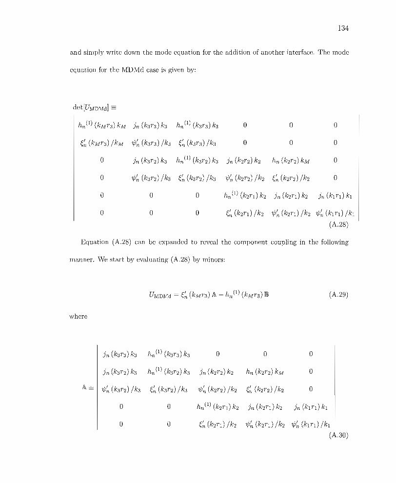
134
and simply write down the mode equation for the addition of another interface. The mode
equation for the MDMd case is given by:
det[UMDMd] ::=
hn (1) (kMT3) kM jn (k3T3) k3 hn (1) (k3T3) k3 0 0 0
~~ (kMT3) /kM 'lj;~ (k3T3) /k3 ~~ (k3T3) /k3 0 0 0
0 jn (k3T2) k3 hn (1) (k3T2) k3 jn (k2T2) k2 hn (k2T2) kM 0
0 'lj;~ (k3T2) /k3 ~~ (k3T2) /k3 'lj;~ (k2 T2) / k2 ~~ (k2T2) /k2 0
0 0 0 hn (1) (k2T1) k2 jn (k2 T1) k2 jn (k1T1) k1
0 0 0 ~~ (k2T1) /k2 'lj;~ (k2T1) /k2 'lj;~(k1T1)/k1
(A.28)
Equation (A.28) can be expanded to reveal the component coupling in the following
manner. We start by evaluating (A.28) by minors:
(A.29)
where
jn (k3T3) k3 hn (1) (k3 T3) k3 0 0 0
jn (k3T2) k3 hn (1) (k3T2) k3 jn (k2T2) k2 hn (k2T2) kM 0
A::= 'lj;~ (k3T2) /k3 ~~ (k3T2) /k3 'lj;~ (k2T2) /k2 ~~ (k2T2) /k2 0
0 0 hn (1) (k2T1) k2 jn (k2T1) k2 jn (k1 Td k1
0 0 ~~ (k2Td /k2 'lj;~ (k2Td /k2 'lj;~(k1Td/k1
(A.3O)

135
and
7/J~ (k3T 3) / k3 ~~ (k3T 3) /k3 0 0 0
jn (k3T 2) k3 hn (1) (k3T2) k3 jn (k2T2) k2 hn (k2T2) kM 0
Iffi::.:: 7/J~ (k3T2) / k3 ~~ (k3T2) /k3 7/J~ (k2T2) / k2 ~~ (k2T2) /k2 0
0 0 hn (1) (k2TI) k2 jn (k2TI) k2 jn (kITd kI
0 0 ~~ (k2Td / k2 7/J~ (k2 Td / k2 7/J~ (k lTd / kl
(A.31)
A second evaluation by minors gives us the equations:
(A.32)
Iffi = 7/J~ (k3T3) / k3C - ~~ (k3T3) / k3]}) (A.33)
where
hn (1) (k3T2) k3 jn (k2T2) k2 hn (k2T2) kM 0
~~ (k3T2) / k3 7/J~ (k2T2) / k2 ~~ (k2T2) / k2 0C= (A.34)
0 hn (1) (k2Td k2 jn (k2TI) k2 jn (kITI) kI
0 ~~ (k2Td / k2 7/J~ (k2TI) /k2 7/J~ (klTd /kI
and
jn (k3T2) k3 jn (k2T2) k2 hn (k2T2) kM 0
7/J~ (k3T2) /k3 7/J~ (k2T2) /k2 ~~ (k2T2) / k2 0]})= (A.35)
0 hn (1) (k2TI) k2 jn(k2TI)k2 jn (kI Td kl
0 ~~ (k2TI) /k2 ?j)~ (k2TI) /k2 7/J~ (kITI) /k l

Thus, equation (A.28) can be written out as:
det[UMDMd] =
~~ (kMr3) [In (k3r3) k3C - hn(1) (k3r3) k31I})]
-hn(1) (kM r3) [W~ (k3r3) /k3C - ~~ (k3r3) /k31I})]
= [~~ (kMr3)jn (k3r3) k3 - hn(1) (kMr3) W~ (k3r3) /k3] C
[ ~~ (kMr3) hn(1) (k3r3) k3 - hn(1) (kM r3) ~~ (k3r3) /k3] II})
This equation can be written as the following determinate:
136
(A.36)
~~ (kM r3) hn(1) (kMr3)
det[UMDMd] = W~ (k3r3) /k3 In (k3r3) k3
~~ (kM r3) hn(1) (kMr3)
hn(1) (k3r3) k3 ~~ (k3r3) /k3
(A.37)
And at this point we recognize that, from equation (A.21):
det[UMd] = (A.38)
and that from equation equation (A.27):
hn(1) (k3r2) k3 In (k2r2) k2 hn (k2r2) kM 0
~~ (k3r2) /k3 W~ (k2r2) /k2 ~~ (k2r2) / k2 0det[UMDm] = C = (A.39)
0 hn(1) (k2r1) k2 In (k2 r1) k2 In (k1rd k1
0 ~~ (k2rd /k2 W~ (k2rd /k2 W~ (k1 rd /k1
with the definitions:
~~ (kM r3) hn(1) (kMr3)(A.40)det[VMd] ==
hn(1) (k3r3) k3 ~~ (k3r3) /k3

137
and
jn (k3T2) k3 jn (k2T2) k2 hn (k2T2) kM 0
VJ~ (k3T2) /k3 VJ~ (k2T2) / k2 ~~ (k2T2) /k2 0det [WMDm] == ill) = (A.41)
0 hn (1) (k2Td k2 jn (k2Td k2 jn (k1Td k1
0 ~~ (k2Td / k2 VJ~ (k2Td / k2 VJ~ (k1Td /k1
We can finally rewrite equation (A.28) as:
!VMdl
IWr"mm I IUMDm I(A.42)
This shows that the on-diagonal elements are the uncoupled modes of the single sphere
(UMd) and the MDm cavity (UMDm ) coupled through the off-diagonal elements VMDm and
VivId·
Asymptotic Expansion of VMd
7]m( (kdT3) ((km T3)
hn (1) (kdT3) hn (1) (km T3)
(A.43)
(A.44)
(A.45)

138
1
i- 2n+1 ~m___eikor3 einmkor3
kOT3
1
1
(A.46)
T3 = S + L + T
nm
= i( _1)n eikor3(1+n:n) (nm
_ 1) e-nm"kor3
kOT3
(A.47)

139
APPENDIX B
RECURSIVE CALCULATION OF SPHERICAL SCATTERING
In this appendix we briefly outline the recursive approach to calculating the scattering
from an arbitrary, L shelled scattercr. We can write the fields in the tth medium as
E~ - ~ ~E 2n + 1 (( b e) 1I~1 (3) e 'N~ (3) ,eM~ (1) d t 'N~ (1))L - ~ nn(n + 1) - n 0111 + an ~ eln + en 0111 - n ~ c111
H~ 2:00 H~ 2n + 1 ( eM~ (3) 'b eN~ (:1) eM~ (1) 'b eN~ (1))L = n ( ) an e1n + ~ n oln + an e1n + ~ n olnnn+1
n-1(D.1)
Figure B.l.. Geometry and labels of an L shell system.

140
Using the same approach as in appendix A, the orthogonality of the vector spherical
harmonics yield a set of 2£ linear equations:
Cn (H1)'l/Jn (mH1Xe) - bn(H1)~n (mH1Xe) - Cn(e)'l/Jn (meXe) + bn(e)~n (mH1Xe) = 0
(B.2)
With the additional boundary conditions for in innermost shell (.e = 1) and finite field
at infinity (.e = £ + 1):
Cn(L+1) = dn (L+1) = 1(B.3)
an (1) = bn (1) = 0
with the following substitutions into equation (B.2 )
(B.4)
it can be rewritten as:
cn (H1)me+1'I/Jn (mH1 Xe) - bn (H1)mH1En (mH1Xe) - cn(e)me'I/Jn (mexe) + bn(e)me~n (mH1Xe) = 0
(B.5)

141
an (Hi) ~~ (mHiXe) - dn(Hi)'ljJ~ (mHiXe) = an (e) mHi ~~ (mexe) - dn(e) mHi 'ljJ~ (mexe)me me
an (Hi) ~n (mHiXe) - dn(Hi)'ljJn (mHiXe) = an (e) mHi ~n (mexe) - dn(e) mHi 'ljJn (mexe)me me
bn(Hi)~n (mHiXe) - cn(Hi)'ljJn (mHiXe) = bn(e)mHi ~n (mexe) - cn(e)mHi'ljJn (mexe)me me
bn(Hi)~~ (mHixp) - cn(Hi)'ljJ~ (mHixp) = bn(e) mHi ~~ (mexp) - cn(P) mHi 'ljJ~ (mexe)me me
(B.6)
which can be reorganized into a coupled set of recursion relations for the TM inward
propagating d~ and outward propagating a~ modes.
an (Hi) ['ljJn (mHixp) ~~ (mHixp) - 'ljJ~ (mHiXe) ~n (mHiXe)] =
an (P) [m~:i 'ljJn (mHiXe) ~~ (mpxp) - 'ljJ~ (mHixp) ~n (mexe)] (B.?)
-dn(e) [m~:i 'ljJn (mHiXe) 'ljJ~ (mexe) - 'ljJ~ (mHiXe) 'ljJn (mpxp)]
-dn(Hi) ['ljJ~ (mHixp) ~n (mHiXe) - 'ljJn (mHixp) ~~ (mHiXe)] =
an (e) [m~:i ~n (mHixp) ~~ (mexe) - ~~ (mHixp) ~n (mexp)] (B.8)
-dn(e) [m~:i ~n (mHiXe) ?j)~ (mpxp) - ~~ (mHixp) 'ljJn (mexe)]
And the corresponding TE field components:
bn(Hi) [~n (mHiXe) 'ljJ~ (mHixp) - ~~ (mHiXe) 'ljJn (mHixp)] =
bn(e) [m~:i 'ljJ~ (mHiXe) ~n (mpxp) - 'ljJn (mHiXe) ~~ (mpxe)] (B.9)
-en(P) [n~:l'ljJ~ (mHixp) 'ljJn (mexp) - 'ljJn (mHixp) 'ljJ~ (mpxe)]

(B.IO)
142
-Cn (HI) [~~ (mHlxe) 1./Jn (mHIXe) - ~n (mHIXe) 1./J~ (mHIXe)] =
bn(e) [m~:l ~~ (me+lXe) ~n (mexe) - ~n (me+lXe) ~~ (mexe)]
-cn (e) [m~:l ~~ (mHIXe) 1./Jn (mexe) - ~n (mHIXe) 1./J~ (mexe)]
Division of (B.7) by (B.8) and (B.g) by (B.IO) yields the needed recursion relations for
TM:
An(HI) =
(An (e) [m~:l 1./Jn (mHIXe) ~~ (mexe) - 1./J~ (mHIXe) ~n (mexe)]
- [m~:l 1./Jn (mHIXe) 1./J~ (mexe) - 1./J~ (mHIXe) 1./Jn (mexe)])/
(An (e) [m~:l ~n (mHIXe) ~~ (mexe) - ~~ (mHIXe) ~n (mexe)]
- [~:l ~n (m€+lXe) 1./J~ (mexe) - ~~ (mHIXe) 1./Jn (mexe)])
and TE modes:
Bn(Hl) =
(Bn(e) [m~:l 1./J~ (m€+lXe) ~n (mexe) - 1./Jn (m€+lXe) ~~ (mexe)]
- [m~:l 1./J~ (mHIXe) 1./Jn (mexe) - 1./Jn (mHIXe) 1./J~ (mexe)])
(Bn(e)mHl~~ (mHIXe)~n (mexe) - ~n (m€+lXe)~~ (mexe)]me
- [~:l ~~ (mHIXe) 1./Jn (mexe) - ~n (mHIXe) 1./J~ (mexe)]
The below logarithmic derivatives are used for their computational stability:
D ( ) = 1./J~(z)n z 1./J~ (z)
F ( ) = ~~(z)n Z ~~(z)
(B.ll)
(B.12)
(B.13)

143
Finally, we rewrite (B.ll) and (B.12) with the following substitution:
An (HI) == An(g) ~n (mgxg)?/In (mgxg)
13(Hl) = B (g) ~n (mgxg)n - n ?/In (mgxg)
(B.14)
To arrive at the recursion relation that can be implemented in our computer algorithm.
An (l) == a(B.15)
Bn (l) == a
For £ < L + 1:
An (HI) = ?/In (mHI Xe) ~n (mHl xHl)
?/In (mHl xHr) ~~ (mHI Xe)Jr;";(e) [~Fn (mgxg) - Dn (meHxg)] - [~Dn (mexe) - Dn (mHIXg)]
An (g) [m~:l Fn (mexg) - Fn (mHl xe)] - [m~:l Dn (mgxe) - Fn (mHI Xg)]
Bn(HI) = ?/In (mHl xg) ~n (mHl xHl)
?/In (mHl xHl) ~~ (mHl xg)B;;(e) [~Dn (mHIXe) - Fn (mexe)] - [~Dn (mg+lxg) - Dn (mgxg)]
Bn(e) [m~:l Fn (mHI Xg) - Fn (mexg)] - [m~:l Fn (mg+lxg) - Dn (mgxe)]
And to calculate the scattered fields, £ = L + 1:
(B.16)
(B.J 7)
Bn
(L+l) = 1/Jn (xL) B;;(L) [dz Dn (XL) - Fn (mLxL)] - [~Dn (XL) - Dn (mLxL)]
~n (xL) Bn(L) [~L Fn (XL) - Fn (mLxL)] - [~L Fn (XL) - Dn (mLxL)](B.19)

144
APPENDIX C
FEM ANALYSIS OF PERIODIC PLASMONIC STRUCTURES
Setup of FEM Model
Within the framework of the finite element method (FEM) we simulate the electro-
magnetic properties of the discretized computational domain shown in figure C.1 (left).
FEM is a frequency domain method approximating of the solution of a PDE over a
closed domain D, with simplified basis functions (second order polynomials) on aN
discrete set of N subdomains dD i , where D = UdD i [119]. This discretized set ofi=l
domains can be seen in figure C.1 (left) as light gray lines forming the system free
mesh. Through its efficient use of free meshing to divide D into dD i , FEM analysis is
well suited to the discretization of problems with complex geometries.
In the context of electromagnetic waves coupled to SPPs, we are concerned with
solving the Helmholtz equation for TM polarized waves:
\7(c(~) \7Hz) - (~r Hz = 0
V· Hzz = 0
(C.la)
(C.lb)
in the periodic domain of figure C.1; In this periodic system, solving Maxwell's
equations reduces to finding the allowed eigenfrequencies, WkJ for a set of Block plane-

145
PMLPort 1
Air
Ag 5i02
Ag
Port 2
PML
Figure C.l. (left) Geometry and free mesh of the computational domain used inthis study. (right) Total energy density plots of (a) an interior surface plasmonmode (kx = 0, w = 1.54PHz). (b) an external surface plasmon mode (kx = 0.5,w = 1.57PHz). (c) a localized substrate plasmon mode(kx = 0, w = 1.97PHz).

146
waves spanning the irreducible Brillouin zone [120]. Because of our use of strongly
dispersive metals, we cannot ignore the dependence of E: on w. This reduces the
solution of (C.1) to a nonlinear eigenvalue problem with the form [120,121]:
(C.2)
The nonlinear nature of the eigenvalue problem can make the FEM conversion
elusive. We solve this problem by first linearizing the eigenvalue problem at an initial
frequency Wo [122]. Because there exists an infinite number of eigenvalue solutions
for a given wo, the solution closest to Wo must be carefully chosen and iterated upon
to retrieve the true eigenvalue Wk. Using the commercially available software COl'vl
SOL [122] this approach is implemented with a two step process: First an eigenmode
is found by solving the linearized eigenvalue problem at an in initial Woo Next, the
eigenmode is used to initialize an iterative Newton's method nonlinear solver to find
the true eigenfrequency Wk. This approach is easily extended to tracing the band
structure over the first Brillouin zone by repeated application of the iteration step
while the x-component of the parameterizing Bloch vector, k = JEdko(sin Bx+cos By),
is slowly varied from 0 to 7f / a. The boundary conditions are set by the Bloch phase
constraint, HA2) = Hz(l)e-ikR, where the Hz(X) enumerates the field at the peri
odic boundaries 1 and 2 from figure C.l. Using COMSOL's MATLAB [123] interface,
a control script is used to slowly alter the boundary conditions between each iteration
by changing kx ' We achieve rapid convergence to the new eigenfrequency, Wk', by us-

147
ing the previous solution for the (Wk, Hz (x, y)) as the initial guess for each iteration
step[122]. An example of this script can be found below.
Computational Geometry
Shown on the left hand side of figure C.1 are the geometry and discretized mesh
of the FENI computational domain. Through our use of periodic boundary conditions
we are representing an infinite array of close-packed silica cylinders with radius rl'
The index of refraction used for all silica regions was nd = 1.42. The rods form a
I-dimensional crystal of periodicity a = 2rl which rests upon a semi-infinite silica
substrate. The cylinders are layered in the positive half-plane with concentric cylin
drical shells defined by their radii (r2, r3 and r4) or corresponding shell thickness
S = Ir2 - rll, L = Ir3 - r21, T = Ir4 - r31 and their constituent material optical prop
erties. When truncated at the intersection of the adjacent cylinder's shell, the "shells"
in fact form a conformal layer along the surface of the cylinder array. By specifying
that the layers are silver, silica and silver we form a uniquely modulated MDM ge
ometry simultaneously supporting the three distinctive electromagnetic eigenmodes
shown in figures C.1(a)-(c). These modes can be placed into the three classes that
we have seen in the case of the MDM sphere: exterior surface plasmons (EPS) along
the silver-air interface and the substrate silica-air interface, interior surface plasmons
(ISP) confined to the dielectric layer between the adjacent metal films and associated
with the coupled plasmons of the two interior silver-silica interfaces, and localized

148
surface plasmon (LSP) modes associated with the excitation of plasmons at the cusps
formed by the intersections of rods or layers.
Silver was chosen in these simulations because it has the lowest losses in the
visible/NIR spectral region. As described in chapter II, we use the standard Drude
model to characterize the dispersion of the silver film. However, due to the conventions
of the COMSOL application we re-express cm(w) in terms of conductivity:
.CJ(W)c(w) = Cr - 'l-
COW
()CJde
CJW =---1 + iTW
(C.3a)
(C.3b)
The astute reader may note the negative imaginary part of Cm (w). This may look
odd to physicists, but it is not incorrect. It is merely the engineering convention
used by COMSOL [122]. The best fit parameters used were: C = 4.1, CJde = 62S/m
and T = 4 . 1O-14S. In this study we choose to focus on a specific geometry with
1'1 = 300nm, S = 30nm, L = 100nm, and T = 15nm. As found in chapter IV the
strength of the SPP coupling between layers is governed by an exponential decay
characterized by silvers skin depth (0 rv 25 nm). The width of the silver layers was
chosen to allow significant coupling between the three mode types, while remaining
thick enough to support well defined eigenmodes such as shown in figure C.1 (a)- (c).
The intersections of the spheres and layers with computational boundaries have
been rounded (2.5nm radius) to reduce instabilities in the computation associated
with infinitely sharp cusps. This results in 'necked' intersections with the boundaries
and the substrate. A situation that is in fact, closer to real physical systems.

149
The size of the silica spacer, L = 100nm, was chosen to be small enough to
constrain SPP excitations in the dielectric gap to be of the symmetric TM, or long
range SPP type [23]. As shown in chapter II, interaction of the two metal surfaces
splits the single interface SPP into a symmetric and anti-symmetric pair. However, the
anti-symmetric TM mode is forbidden when L ;S A/(2nd), where nd = JEd is the gap
dielectric refractive index [124]. Thus, for the L = 100 nm rv A/10 geometry simulated
here, we are well within the regime of exclusive symmetric TM SPP propagation.
Boundary Conditions
Periodic Flouqet-Bloch boundary conditions were employed at the left and right
boundaries to simulate an infinite array of MDM coated cylinders. In FEM this
boundary condition is implemented by employing a Bloch phase constraint H(l)e-iKR =
H(2) on the tangential field components (Hz and Ey ) at the periodic boundaries 1
and 2, where the reciprocal lattice vector K = 27r/a· x and R = a· x.
Typical in FEM, the open boundary conditions of scattering problems are difficult
to correctly simulate. To overcome this difficulty we utilized perfectly matched layers
1.2/'-Lm long, at the top and bottom of the computational domain [119]. This allowed
the simulation of far-field plane-wave scattering, while inducing a minimum amount
of error due to artificial reflections from computational boundaries.
Mesh parameters
Care must be taken when modeling metallic nanosystems due the rapid decay of
the evanescent field near the metal surface. We were careful to select a mesh size that

150
(a) (b) (c) 1.97eV 1.97eV
~A9
~SiO,-FEM
-SchreIer
Energy (eV) 2.2
~Ag
, SIO, _FEM I-Schroter
TT '·1 ._, .-
1.0
1.4 Energy (eV) 2.2
1.0 ""'I I\..c ----------''S;:.;:::;U<IJ
<;::<IJcr:
- Analytic Transmission 0.0- Analytic Reneclion 1.4
• FEM TM Transmission• FEM 1M Reflection
400 4~ 500 5~ 600 600 roo 750 BOO
06
0.9
0.7
0.4
0.1
0.3
0.5
0.2
0.6
Figure C.2. (a) Comparison of FEM with analytic calculation for normal transmission and reflection through (a) a 27nm thick silver film in air and, (b) cLsyrnrnctrically(top) and conformally (bottom) modulated sinusoidal silver films from [125]. (c) Efield intensity comparison with Schroter [125] at nw = 1.97 eV. The reflectivity dipat 1.97 eV shows the excitation of a SPP on the air-silver interface.
minimized the computational error while keeping the computation time tractable.
Typical mesh sizes of four elements per decay length (skin depth) of 20nm, or a
element linear dimension of 5nm, where used near the metal-dielectric interface and
inside metal domains. Outside of the metal subdomains, a conservative'" AI (20nd)
mesh size (30nm typical) was used. Mesh convergence tests showed that this was
sufficient to maintain an estimated computational precision of approximately one
percent.
To estimate the solution accuracy as a function of mesh size, an FEM simulation
of a 27nm metal film was discretized using the same constraints and transmission
calculations were compared to the the analytic solution [114]. This is shown in fig-

151
ure C.2(a). Additionally we have examined the accuracy of the FEM mesh condi-
tions with comparison to Schroter and Heitmann [125]. They have used an analytical
method based on coordinate transforms and the transfer-matrix method, to calculate
the transmission of light through modulated thin silver films on silica substrates. The
accurate reproduction of their results can be found in figures C. 2(b) and (c).
MATLAB Band Diagram Script
The following MATLAB scripts can be used to generate the reflection, transmis-
sion and mode diagrams of dispersive periodic structures. Having setup your fern
structure (geometry, sub-domain parameters and mesh) using COMSOL, input it
into the MATLAB command interface (CTRL-F) and run the following scripts in the
order in which they are shown below.
Initial Frequency Sweep
I function [omegaSolnSort, rtfems, rtfullfem] = evFreqSweep(fem, OmegaRange, kstart, TOL)2
3 %Set the search parameters in frequency space4 delOmega = OmegaRange(3);5 OmegaStart = OmegaRange (1) ;
6 OmegaStop = OmegaRange(2);7 omegaVector = OmegaStart:delOmega:OmegaStop;8 omegaSoln = [];9
10
II %Update magnitude of k12 fem.const{2*strmatch('k' ,fem.const(1:2:end), 'exact')} = kstart;13
14 % Initial solution to eigenvalue problem15 counter = 1;16 omegaSoln = [];17
18 for ind=l :length(omegaVector)19 fprintf(l, 'Initalvalue: %g' ,omegaVector(ind));20
21 fem,appl{1}.prop.analysis = 'eigen';22 fern = multiphysics(fem);

23 fem.xmesh = meshextend(fem);24
25 init = asseminit(fem, 'init' J '0');26 try27 fem.sol=femeig(fem, ...28 'init' ,init, ...29 'complexfun' ,'on' J •••
30 ) conjugate J , 'on) ,31 'solcomp' ,{'Hz'}, ...32 'neigs',l, ...33 'shift' ,-i*omegaVector(ind),34 'linsolver', 'pardiso' J •••
35 'maxeigi t) J 100 J •••
36 'eigref' ,sprintf('-i*%g' ,0megaVector(ind»);3738 % Store solution guess for all bands39 catch40 fprintf(l,'---NO EVs near %g\n',omegaVector(ind));41 continue;42 end43
44 fprintf(l, '--EV-->%g' ,-imag(fem.sol.larnbda);45
46 fem.appl{l}.prop.analysis = 'harmonic';47 fern = multiphysics(fem);48 fem.xmesh = meshextend(fem);49
50 %Final refinment of inital EVs using the nonlinear51 %interative solver52 init = asseminit(fem, 'u' ,fem.sol);53 try54 [fern. sol stp]=femnlin(fem,55 ) ini t ' , ini t J •••
56 'linsolver' J 'pardiso' J
57 'complexfun' J 'on' J •••
58 'conjugate' J 'on' J'"
59 ' sol comp' , { 'Hz' , 'freq'} ,60 'outcomp' ,{'Hz' ,'freq'},61 ' out', {' sol', , st op'}, ...62 'Ntol', le-l);63 catch64 fprintf(l, '--->No eigenfrequency found, skipping\n');65 continue;66 end67 tempom = postint(fem, 'nu_rfwh', 'edim' ,O,'dl' ,1,'solnum','all')*2*pi;68 tempwt = abs(real(tempom) - omegaVector(ind));69 if(stp-=O)70 fprintf(l,'Did not converge, skipping %g\n' ,ternporn);71 continue;72 else73 fprintf(l,'--NL-->%g' ,ternporn);74 end75
76 if (counter>l)77 if ( abs«omegaSoln(counter-l)-ternpom)/omegaSoln(counter-l)) > TOL)78
152
79
80
81
82
8:J
84
85
omegaSoln (counter) =temporn;wt(counter) = tempwt;initset{counter} = init;femset{counter} = fem.sol;counter = counter + 1;fprintf(l,'-->New, Keeping\n');

86 elseif(wt(counter-1»tempwt)87
88 omegaSoln(counter-1)=tempom;89 initset{counter-1} = init;90 femset{counter-1} = fern. sol;91 wt(counter-1) = tempwt;92 fprintf(l,'-->Closer, Keeping\n');93
94 else95 fprintf(l, '-->Repeat, Skipping\n');96 end97 else98 omegaSoln(counter) = tempom;99 wt(counter) = tempwt;
100 initset{counter} = init;101 femset{counter} = fern. sol;102 counter = counter + 1;103 fprintf(l, '-->First, Keeping\n');104 end105 end106
107 omegaSolnSort = omegaSoln;108 rtfems = femset;109 rtinits = initset;lID rtfullfem = fern;III end
Iteration of Initial Eigenvalues
function [evList, femOutJ = evIterate(femStruct, femSolIn, evIn)2
3 TOL = 1e-6; % Tolerance for floating point comparison4
5 %Final refinment of inital EVs using the nonlinear6 %interative solver7
8 % Ensure harmonic analysis, and an extended mesh9 femStruct.appl{l}.prop.analysis = 'harmonic';
10 femStruct = multiphysics(femStruct);II femStruct.xmesh = meshextend(femStruct);12
13 %Container varibles for solution results14 omegaO =[J ;15 sol = {};16 counter = 1;17 numoms = length(femSolIn);18
19 for ind=l:numoms % Iterate on the reduced set of k=O EVs20
21 fprintf(l, 'Refining %i!%i, Inital eigenfrequency[HzJ: %g+i*%g', ...22 ind,numoms, real(evIn(ind»,imag(evIn(ind»);23
24 %Construct the inital mesh solution to seed the nonlinear sovIer25 evsol = femsol(femSolIn{ind}.u, 'lambda', evIn(ind»;26 init = asseminit(femStruct, 'init', evsol);27
28 try29 femStruct.sol=femnlin(femStruct,30 ) ini t ) J ini t J •••
153

3] Jlinsolver', 'pardiso' J
32 'cornplexfun' J 'on' J •••
33 'conjugate', 'on', ...34 'solcomp' ,{'Hz', 'freq'},35 'outcomp' ,{'Hz' ,'freq'});36
37 catch38 fprintf(1,'--->Refinement Failed, skipping\n');39 continue;40 end41
42 sol{counter} ~ femStruct.sol;43 omegaO(counter)~ postint(femStruct,'nu_rfwh' ,'edim' ,0, 'dl' ,1,'solnum','all')*2*pi;44 fprintf(1,'--->%g+i*%g\n' ,real(omegaO(counter)),imag(omegaO(counter)));45 counter = counter + 1;46 end47
48 [evList, ommaskJ ~ remDups(omegaO,TOL);49 Possiblelndex ~ 1:length(ommask);50 maskvector ~ Possiblelndex(logical(ommask));51 evList evln(maskvector);52 femOut ~ sol (maskvector) ;53
54 end
Band Trace
154
function [bandenergy, bandkvaluesJ
newtmin ~ 1e-8;
BandTrace(fem, omegaln, femSolln, KL)
4
5 kstart ~ KL(1);6 kend~KL(2);
7 kdel ~ KL(3);8 kminf actor ~ 10;9 klist ~ kstart:kdel:kend;
10
11 fprintf(1, 'Calculating Band Structure:\n');12
13 bandenergy ~ cell(1,length(omegaln));14 bandkvalues ~ cell(1, length(omegaln));15 counter ~ 1;16
17 mkdir (' femsolsTM') ;18 save(sprintf('femsolsTM/femfull_kstart%2.1f.mat' ,kstart), 'fern');19
20 for ind~1:length(omegaln)
21 fprintf(1,'Starting at ev:%g--->' ,omegaln(ind));22
23
24
25
26
27
28
29
30
31
32
evsol ~ femsol(femSolln{ind}.u, 'lambda', omegaln(ind));init ~ asseminit(fem, 'init', evsol);
fem.sol~femnlin(fem,
, ini t ) J ini t J •••
'cornplexfun' J 'on' J •••
'conjugate' J 'on', '"'solcomp' ,{'Hz' ,'freq'},'outcomp',{'Hz' ,'freq'},'pname' J 'k', ...

33
34
35
36
37
38
39
40
41
42
43
44
45
'plist' ,klist, ...'pinitstep' ,abs(kdel) ,'pminstep',abs(kdel)/kminfactor,'pmaxstep',abs(kdel),'oldcomp' , {}, .'porder' ,OJ .'Maxiter' ,50, .Jminstep' ,newtmin,'linsolver', 'pardiso');
bandenergy{counter} = postint(fem,'nu_rfwh', 'edim' ,0, 'dl' ,1, 'solnum', 'all')*2*pi;bandkvalues{counter} = fem.sol.plist;
155
46 %save the data47 fprintf(l,'Saving Data-->');48 femsolu = fern. sol;49 eigenfreq = bandenergy{counter};50 kvector = bandkvalues{counter};51 save(sprintf('femsolsTM/band%d_femsol_kstart%2.1f.mat' ,counter,kstart), 'femsolu');52 save(sprintf('femsolsTM/band%d_energy_kstart%2.1f.mat' ,counter,kstart), 'eigenfreq');53 save(sprintf('femsolsTM/band%d_kvector_kstart%2.1f.mat' ,counter,kstart), 'kvector');54 counter = counter +1;55 fprintf(l, 'Done\n');56
57 end58
59 save(sprintf('bands_kstart%2.1f.mat' ,kstart), 'bandenergy', 'bandkvalues');60
6J end
156
BIBLIOGRAPHY
[1] S. Maier, Plasmonics: Fundamentals and Applications (New York: Springer,2007).
[2] A. Sommerfeld, Wiedemanns Annalen 67, 233 (1899).
[3] J. Zenneck, Annalen Physik 23, 846 (1907).
[4] G. Mie, Annalen Physik 25, 377 (1908).
[5] R. Wood, Proceedings of the Physical Society of London 18, 269 (1902).
[6] M. Faraday, Philosophical Transactions of the Royal Society of London 147,145 (1857).
[7] lSI Web of Knowledge, URL http://www.isiknwoledge.com/.
[8] U. Fano, Journal of the Optical Society of America 31, 213 (1941).
[9] R. Ritchie, E. Arakawa, J. Cowan, and R. Hamm, Physical Review Letters 21,1530 (1968).
[10] R. Ritchie, Physical Review 106, 874 (1957).
[11] C. Powell and J. Swan, Physical Review 118, 640 (1960).
[12] M. Daniel and D. Astruc, Chemical Reviews 104, 293 (2004).
[13] Fraday Museum Royal Insitution (2008), URL http://www .rigb. org/.
[14] G. Moore, Electronics Journal 38, 114 (1965).
[15] vV. Barnes, A. Dereux, and T. Ebbesen, Nature 424, 824 (2003).
[16] J. Homola, S. Yee, and G. Gauglitz, Sensors and Actuators B 54, 3 (1999).
[17] C. Loo, A. Lowery, N. Halas, J. West, and R. Drezek, Nano Letters 5, 709(2005).
[18] M. Seydack, Biosensors and Bioelectronics 20, 2454 (2005).

157
[19] T. Ebbesen, H. Lezec, H. Ghaemi, T. Thio, and P. Wolff, Nature 391, 667(1998).
[20] R. Charbonneau, P. Berini, E. Berolo, and E. Lisicka-Shrzek, Optics Letters25, 844 (2000).
[21] M. Quinten, A. Leitner, J. Krenn, and F. Aussenegg, Optics Letters 23, 1331(1998).
[22] S. Maier, P. Kik, H. Atwater, S. Meltzer, E. Harel, B. Koel, and A. Requicha,Nature Materials 2, 229 (2003).
[23] J. Dionne, L. Sweatlock, H. Atwater, and A. Polman, Physical Review B 73(2006).
[24] G. Veronis and S. Fan, Applied Physics Letters 87 (2005).
[25] R. Zia, M. Selker, P. Catrysse, and M. Brongersma, Journal of the OpticalSociety of America A 21, 2442 (2004).
[26] S. Bozhevolnyi, V. Volkov, E. Devaux, J. Laluet, and T. Ebbesen, Nature 440,508 (2006).
[27] R. Charbonneau, N. Lahoud, G. Mattiussi, and P. Berini, Optics Express 13,977 (2005).
[28] 1. Smolyaninov, D. Mazzoni, J. Mait, and C. Davis, Physical Review B 56, 1601(1997).
[29] L. Yin, V. Vlasko-Vlasov, J. Pearson, J. Hiller, J. Hua, U. Welp, D. Brown,and C. Kimball, Nano Letters 5, 1399 (2005).
[30] H. Ditlbacher, J. Krenn, G. Schider, A. Leitner, and F. Aussenegg, AppliedPhysics Letters 81, 1762 (2002).
[31] V. M. Shalaev, Nature Photonics 1, 41 (2007).
[32] D. Smith, J. Pendry, and M. Wiltshire, Science 305, 788 (2004).
[33] V. Lomakin, Y. Fainman, Y. Urzhumov, and G. Shvets, Optics Express 14,11164 (2006).
[34] J. Pendry, Physical Review Letters 85, 3966 (2000).
[35] A. Alu and N. Engheta, IEEE Transactions on Antennas and Propagation 51,2558 (2003).

158
[36] U. Leonhardt, Science 312, 1777 (2006).
[37] J. Pendry, D. Schurig, and D. Smith, Science 312,1780 (2006).
[38] C. Enkrich, M. Wegener, S. Linden, S. Burger, L. Zschiedrich, F. Schmidt,J. Zhou, T. Koschny, and C. Soukoulis, Physical Review Letters 95 (2005).
[39] V. Veselago, Soviet Physics Uspekhi-Ussr 10, 509 (1968).
[40] A. Grbic and G. Eleftheriades, Physical Review Letters 92 (2004).
[41] R. Shelby, D. Smith, and S. Schultz, Science 292, 77 (2001).
[42] T. Yen, W. Padilla, N. Fang, D. Vier, D. Smith, J. Pendry, D. Basov, andX. Zhang, Science 303, 1494 (2004).
[43] A. Grigorenko, A. Geim, H. Gleeson, Y. Zhang, A. Firsov, 1. Khrushchev, andJ. Petrovic, Nature 438, 335 (2005).
[44] A. Alu and N. Engheta, Journal of the Optical Society of America B 23, 571(2006).
[45] H. Shin and S. Fan, Physical Review Letters 96 (2006).
[46] C. Rohde, K. Hasegawa, and M. Deutsch, Optics Letters 32, 415 (2007).
[47] D. Schurig, J. J. Mock, B. J. Justice, S. A. Cummer, J. B. Pendry, A. F. Starr,and D. R. Smith, Science 314, 977 (2006).
[48] 1. Smolyaninov, Y. Hung, and C. Davis, Arxiv preprint arXiv:0709.2862 (2007).
[49] E. Hutter and J. Fendler, Advanced Materials 16, 1685 (2004).
[50] A. Haes and R. Van Duyne, Laser Focus World 39, 153 (2003).
[51] A. Haes, D. Stuart, S. Nie, and R. Van Duyne, Journal of Fluorescence 14, 355(2004).
[52] M. Moskovits, Reviews of Modern Physics 57, 783 (1985).
[53] S. Lofas and B. Johnsson, Journal of the Chemical Society 1990, 1526 (1990).
[54] B. Johnsson, S. LaDs, and G. Lindquist, Analytical Biochemistry 198, 268(1991).
[55] R. Karlsson, A. Michaelsson, and L. Mattsson, Journal of Immunological Methods 145, 229 (1991).

159
[56] U. Jonsson, L. Fagerstam, B. Ivarsson, B. Johnsson, R. Karlsson, K. Lundh,S. Lofas, B. Persson, H. Roos, and 1. Ronnberg, Biotechniques 11, 620 (1991).
[57] A. Haes and R. Van Duyne, Journal of the American Chemical Society 124,10596 (2002).
[58] E. Palik, Handbook of Optical Constants of Solids (Academic Press, 1985).
[59] E. Fontana, IEEE Transactions On Microwave Theory and Techniques 50, 82(2002).
[60] C. Yonzon, E. Jeoungf, S. Zou, G. Schatz, M. Mrksich, and R. Van Duyne,Journal of the American Chemical Society 126, 12669 (2004).
[61] A. McFarland and R. Van Duyne, Nano Letters 3, 1057 (2003).
[62] K. Kneipp, Y. Wang, H. Kneipp, L. Perelman, 1. Itzkan, R. Dasari, and M. Feld,Physical Review Letters 78, 1667 (1997).
[63] S. Nie and S. Emery, Science 275, 1102 (1997).
[64] C. Haynes and R. Van Duyne, Journal of Physical Chemistry B 107, 7426(2003).
[65] C. Rohde, K. Hasegawa, and M. Deutsch, Physical Review Letters 96 (2006).
[66] L. Davis and M. Deutsch, in preparation.
[67] S. Sershen, S. Westcott, N. Halas, and J. West, Journal of Biomedical MaterialsResearch 51, 293 (2000).
[68] S. Pillai, K. Catchpole, T. Trupke, and M. Green, Journal of Applied Physics101, 093105 (2007).
[69] N. Engheta, A. Salandrino, and A. Alii, Physical Review Letters 95, 95504(2005) .
[70] E. Betzig and J. Trautaman, Science 257, 189 (1992).
[71] X. Luo and T. Ishihara, Applied Physics Letters 84, 4780 (2004).
[72] W. Srituravanich, N. Fang, C. Sun, Q. Luo, and X. Zhang, Nano Lett 4, 1085(2004).
[73] E. Altewischer, M. van Exter, and J. Woerdman, Nature 418, 304 (2002).
[74] D. E. Chang, A. S. Sorensen, E. A. Demler, and M. D. Lukin, Nature Physics3, 807 (2007).

160
[75] D. Bergman and M. Stockman, Physical Review Letters 90, 27402 (2003).
[76] E. Prodan, C. Radloff, N. Halas, and P. Nordlander, Science 302, 419 (2003).
[77] H. Raether, Surface Plasmons on Smooth and Rough Surfaces and on Gratings(Springer-Verlag New York, 1988).
[78] E. Economou, Physical Review 182, 539 (1969).
[79] N. Ashcroft and N. Mermin, Solid State Physics (Holt, Rinehart and WinstonNew York, 1976).
[80] B. Prade, J. Vinet, and A. Mysyrowicz, Physical Review B 44, 13556 (1991).
[81] H. Shin, 1!J. Yanik, S. Fan, R. Zia, and M. Brongersma, Applied Physics Letters84, 4421 (2004).
[82] K. Hasegawa, C. Rohde, and M. Deutsch, Optics Letters 31, 1136 (2006).
[83] C. Bohren and D. Huffman, Absorption and Scattering of Light by Small Par-ticles (Wiley, New York, 1998).
[84] A. Aden and M. Kerker, Journal of Applied Physics 22, 1242 (2004).
[85] R. Bhandari, Applied Optics 24, 1960 (1985).
[86] O. Toon and T. Ackerman, Applied Optics 20, 3657 (1981).
[87] 'lv. Yang, Applied Optics 42, 1710 (2003).
[88] V. Cachorro and L. Salcedo, Journal of Electromagnetic Waves and Applications5, 913 (1991).
[89] S. Leder, Y. Takakura, and P. Meyrueis, Optics Letters 30, 2641 (2005).
[90] T. Kaiser and G. Schweiger, Computers in Physics 7, 682 (1993).
[91] D. Zwillinger et al., Standard Mathematical Tables and Formulae (Chapman &Hall/CRC Boca Raton, Fl, 2003).
[92] Z. Wang, B. Luk'yanchuk, M. Hong, Y. Lin, and T. Chong, Physical Review B70 (2004).
[93] T. Kelf, Y. Sugawara, J. Baumberg, M. Abdelsalam, and P. Bartlett, PhysicalReview Letters 95 (2005).
[94] A. Moroz, Physical Review Letters 83, 5274 (1999).

161
[95] S. Oldenburg, R. Averitt, S. Westcott, and N. Halas, Chemical Physics Letters288, 243 (1998).
[96] J. Jackson, S. Westcott, L. Hirsch, J. West, and N. Halas, Applied PhysicsLetters 82, 257 (2003).
[97] A. Alu and N. Engheta, Physical Review E 72 (2005).
[98] S. Mohamed, O. Kappertz, T. Pedersen, R. Drese, and M. Wuttig, PhysicaStatus Solidi A 198, 224 (2003).
[99] R. Ruppin, Physics Letters A 299, 309 (2002).
[100] D. Smith, H. Chang, K. Fuller, A. Rosenberger, and R. Boyd, Physical ReviewA 69 (2004).
[101] A. P. Hibbins, W. A. Murray, J. Tyler, S. Wedge, W. L. Barnes, and J. R.Sambles, Physical Review B 74 (2006).
[102] A. Christ, T. Zentgraf, J. Kuhl, S. Tikhodeev, N. Gippius, and H. Giessen,Physical Review B 70, 125113 (2004).
[103] N. Bonod, S. Enoch, L. Li, E. Popov, and M. Neviere, Optics Express 11, 482(2003).
[104] E. Sanchez, L. Novotny, and X. Xie, Physical Review Letters 82, 4014 (1999).
[105] N. A. Issa and R. Guckenberger, Plasmonics 2, 31 (2007).
[106] VV. Stober, A. Fink, and E. Bohn, Journal of Colloid and Interface Science 26,62 (1968).
[107] H. Giesche, Journal of the European Ceramic Society 14, 205 (1994).
[108] H. Giesche, Journal of the European Ceramic Society 14, 189 (1994).
[109] Deutsch Group Software Repository, URL http://mo .uoregon. edu.
[110] S. Wong, V. Kitaev, and G. Ozin, Journal of the American Chemical Society125, 15589 (2003).
[111] R. Rengarajan, D. Mittleman, C. Rich, and V. Colvin, Physical Review E 71(2005).
[112] D. Hall, P. Underhill, and J. Torkelson, Polymer Engineering and Science 38,2039 (1998).

162
[113] X. Huang, L. Bao, X. Cheng, 1. Guo, S. Pang, and A. Yee, Journal of VacuumScience & Technology B 20, 2872 (2002).
[114] M. Born and E. Wolf, Principles of Optics (Pergamon Press New York, 1980).
[115] A. Haes and R. Van Duyne, Analytical Chemistry 68, 2629 (1996).
[116] C. Haynes and R. Van Duyne, Journal of Physical Chemistry B 105, 5599(2001).
[117] C. Haynes, A. McFarland, M. Smith, J. Hulteen, and R. Van Duyne, Journalof Physical Chemistry B 106, 1898 (2002).
[118] C. Haynes and R. Van Duyne, Nano Letters 3, 939 (2003).
[119] J. Jin, The Finite Element Method in Electromagnetics (Wiley, New York,1993).
[120] B. Hiett, J. Generowicz, S. Cox, M. Molinari, D. Beckett, and K. Thomas, IEEEProceedings on Science Measurement and Technology 149, 293 (2002).
[121] M. Davanco, Y. Urzhumov, and G. Shvets, Optics Express 15, 9681 (2007).
[122] COMSOL Mutliphysics v3.4 (2008), URL http://www.comsol.com.
[123] MATLAB v2007b, URL http://www.mathworks.com/.
[124] 1. Avrutsl\:y, 1. Salakhutdinov, J. Elser, and V. Podolskiy, Physical Review B75 (2007).
[125] U. Schroter and D. Heitmann, Physical Review B 60, 4992 (1999).