Embed Size (px)
Citation preview

OPEN
ORIGINAL ARTICLE
Direct observation of localized surface plasmon fieldenhancement by Kelvin probe force microscopy
Da-Bing Li1, Xiao-Juan Sun1, Yu-Ping Jia1, Mark I Stockman2, Hari P Paudel2, Hang Song1,Hong Jiang1 and Zhi-Ming Li1
A surface plasmon (SP) is a fundamental excitation state that exists in metal nanostructures. Over the past several years, the
performance of optoelectronic devices has been improved greatly via the SP enhancement effect. In our previous work, the
responsivity of GaN ultraviolet detectors was increased by over 30 times when using Ag nanoparticles. However, the physics of
the SP enhancement effect has not been established definitely because of the lack of experimental evidence. To reveal the phy-
sical origin of this enhancement, Kelvin probe force microscopy (KPFM) was used to observe the SP-induced surface potential
reduction in the vicinity of Ag nanoparticles on a GaN epilayer. Under ultraviolet illumination, the localized field enhancement
induced by the SP forces the photogenerated electrons to drift close to the Ag nanoparticles, leading to a reduction of the sur-
face potential around the Ag nanoparticles on the GaN epilayer. For an isolated Ag nanoparticle with a diameter of ~ 200 nm,
the distribution of the SP localized field is located within 60 nm of the boundary of the Ag nanoparticle. For a dimer of Ag nano-
particles, the localized field enhancement between the nanoparticles was the strongest. The results presented here provide direct
experimental proof of the localized field enhancement. These results not only explain the high performance of GaN detectors
observed with the use of Ag nanoparticles but also reveal the physical mechanism of SP enhancement in optoelectronic devices,
which will help us further understand and improve the performance of SP-based optoelectronic devices in the future.
Light: Science & Applications (2017) 6, e17038; doi:10.1038/lsa.2017.38; published online 25 August 2017
Keywords: detector; GaN; KPFM; plasmon
INTRODUCTION
A surface plasmon (SP) is an optical phenomen on that involvescollective oscillations of charges that are confined to nanostructuredmetal systems1. One of the most fundamental properties of a SP isthe localization of the electromagnetic field. By nature, the SPeigenmodes of small nanoplasmonic systems are localized and non-propagating. SP has delivered a number of important applications:ultrasensing2, scanning near-field optical microscopy3, thermallyassisted magnetic recording4, biomedical tests5 and SP-assisted thermalcancer treatment6. Surface plasmon amplification by stimulatedemission of radiation (SPASER), a nanoplasmonic counterpart ofthe laser, was proposed in theory by Bergman and Stockman and hasbeen realized in experiments7–9. Moreover, SP has offered newopportunities to improve the performance of semiconductor optoe-lectronic devices. Metallic nanostructures have been used to modifythe local density of optical states to control light emission, enhancephotoluminescence and reduce the quantum-confined Stark effect inlight emitting diodes (LEDs)10–12. Plasmonic metallic nanoparticleshave also been integrated into photovoltaic devices to increase thesolar cell absorption via light-trapping effects and enhance the short-circuit photocurrent density13–17.
In our previous work, we realized high-performance GaN detectorsby fabricating Ag nanoparticles on the surface of the GaN epilayer;the responsivity of the GaN detectors increased by over 30 times. Thelocalized SP effect was considered the reason for this enhancement18,19,as elaborated in our previous report. Here, the ‘enhancement’ refers toan increase in responsivity of the treated GaN detector and not toan optical electric field intensity increase due to local plasmonicresonance. However, the direct evidence for this hypothesis isstill lacking, and the physical origin behind the SP enhancing theperformance of semiconductor photoelectric devices remains to beclarified. Hence, a feasible method is urgently required to explain theSP enhancement.Here we propose a method to detect the SP-induced localized field
variation of Ag nanoparticles on GaN epilayer using Kelvin probeforce microscopy (KPFM). As an electrical analog of atomic forcemicroscopy (AFM), KPFM is typically used to observe the surfacepotential20–23. The electrical properties, such as the polarity24,25,doping type26,27, homogeneity28 and charge density29 of the sample,have all been identified using KPFM. Based on the theory that thelocalized field enhancement by SP will adjust the dispersion ofthe electrons in the GaN epilayer, KPFM was adopted here to verifythe existence of the plasmon-enhanced field. Under ultraviolet (UV)
1State Key Laboratory of Luminescence and Applications, Changchun Institute of Optics, Fine Mechanics and Physics, Chinese Academy of Sciences, Changchun 130033, Chinaand 2Center for Nano-Optics (CeNO) and Department of Physics and Astronomy, Georgia State University, Atlanta, GA 30340, USACorrespondence: DB Li, Email: [email protected]; XJ Sun, Email: [email protected] 31 January 2017; revised 6 March 2017; accepted 6 March 2017; accepted article preview online 8 March 2017
Light: Science & Applications (2017) 6, e17038; doi:10.1038/lsa.2017.38Official journal of the CIOMP 2047-7538/17www.nature.com/lsa

illumination, the surface potential around a Ag nanoparticle on theGaN epilayer was reduced, thereby providing direct evidence forthe SP-induced localized field enhancement. Our direct observationof the SP effect can open ample avenues to integrate SP into futureoptoelectronic devices.
MATERIALS AND METHODS
The undoped GaN epilayer was grown on a (0001) sapphire substrateusing metal-organic chemical vapor deposition at 1050 °C. Details ofthe GaN epilayer growth can be found in previous work18. The Agnanoparticle was fabricated by electron beam evaporation at a pressureof ~ 5.4 × 10− 6 mbar. The evaporation rate was ~ 0.1 nm s− 1. Next,the sample was annealed at 800 °C for 5 min to form Ag nanoparticles.The Bruker multimode-8 AFM tapping mode was used to characterizethe morphology, and the KPFM mode was used to determine thesurface potential of the Ag nanoparticles on the GaN epilayer. The tipwas a Pt/Ir-coated tip, and the lift height for the interleaved mode wasset to be 100 nm. When we used the KPFM to measure the surfacepotential of the Ag nanoparticles on the GaN epilayer, the laser beamilluminating the tip was reflected on the photodetector. The alternat-ing current (AC) bias was used as an oscillator signal to allow the tipto oscillate at its resonance frequency. The direct current (DC) biaswas used to adjust the amplitude of the oscillation to zero as the lock-in signal. In addition, an external UV source was used to enable themeasurement of the change of the surface potential without and withUV illumination. Time-domain and frequency-domain finite-elementmethods were used to simulate the distribution of electric field of a Agnanoparticle under UV illumination.
RESULTS AND DISCUSSION
A schematic principle of using KPFM to detect the surface potentialis given in Figure 1. In KPFM mode, the tip is driven by the appliedAC at the same frequency as the resonance frequency (ω) of the tip.As the tip scans the sample, it also vibrates. When KPFM is used tomeasure the surface potential of the Ag nanoparticles on a GaNepilayer, the tip lowers such that it is close to the surface of thesample. At this stage, the contact potential (VCPD) appears andmodulates the vibration of the tip. Moreover, there is a directvoltage biased on the tip (Vbias). The values of VCPD and Vbias are
used to determine ΔVDC according to Equation (1).
DVDC ¼ V bias � VCPD ð1ÞThus, the active forces on the tip originate from both the alternating
voltage (VACsin(ωt)) and the directive voltage (ΔVDC)30–32. The
equation for the force is given as follows:
F ¼ �dU
dZ¼ �1
2
dC
dZðDVÞ2 ¼ �1
2
dC
dZðDVDC þ VAC sin ðotÞÞ2 ð2Þ
In succession, Equation (3) can be deduced, where the coefficient ofSin(ωt) is the amplitude of the vibration of the tip.
F ¼ �1
2
dC
dZðDV 2
DC þ 1
2VAC
2Þ � dC
dZDVDCVAC sin ðotÞ
þ 1
4
dC
dZV 2
AC cos ð2ot þ 2jÞ ð3ÞThe KPFM feedback loop is used to adjust the Vbias to be equal to
VCPD and achieve ΔVDC= 0. Thus, when the amplitude is zero andthen the value of VCPD is obtained. In our experiment, the value ofVCPD is the difference between the surface potential of the sample andthe potential of the tip, as given by Equation (4):
VCPD ¼ V Sample � VTip ð4ÞThe relationship among the VCPD, the work functions of the sample
(ϕSample) and the tip (ϕTip) can be written as31,32,
VCPD ¼ fTip � fSample
eð5Þ
According to this relationship, a smaller VCPD corresponds to ahigher ϕSample. Thus, under UV illumination, the decrease of thesurface potential around the Ag nanoparticle corresponds to anincrease of the surface work function.The morphology of the Ag nanoparticles on the GaN epilayer was
measured using AFM in tapping mode. The semi-spherical isolated Agnanoparticles and dimer Ag nanoparticles are located randomly on theGaN epilayer, as shown in Supplementary Figs. S1 and S2. Figure 2ashows the typical morphology of the Ag nanoparticles on the GaNsurface. The red and green lines are marked crossing the isolated Agnanoparticle to describe the characteristics of the Ag nanoparticlesclearly. The diameters of this Ag nanoparticle are 205 and 220 nm,corresponding to the red and green lines, respectively. The height ofthe Ag nanoparticle is ~ 80 nm, according to the section profiles of
UV LEDon/off
Photo-detector
Laser beamLock-in
SumDC bias
AC
Potential signal
Oscillatorsignal
Controller(feedback loopadjusts DC tipbias to zerolock-in signal)
GaN
Ag
Sapphire
Figure 1 Schematic principle of KPFM. The Ag nanoparticles on the GaN substrate were characterized using KPFM. The laser beam illuminating the tip isreflected to the photodetector, and the amplitude signal is detected. The AC bias is an oscillator signal used to allow the tip to oscillate at its resonancefrequency. The DC bias is used to adjust the amplitude of the oscillation to zero as the lock-in signal. In addition, an external UV LED is used to detect thedifference in surface potential without and with UV illumination.
Direct observation of localized surface plasmon fieldDB Li et al
2
Light: Science & Applications doi:10.1038/lsa.2017.38

height given in Figure 2b. For the dimer of Ag nanoparticles, the blackline crosses the two adjacent nanoparticles, as shown in Figure 2a. Forthe left and right nanoparticles of the dimer, the diameters are 278 and229 nm, respectively, with corresponding heights of 70 and 60 nm,respectively.The surface potential of a Ag nanoparticle on GaN was obtained by
AFM using KPFM mode. Figure 2c and 2d, shows the measuredsurface potential in the dark and under UV illumination, respectively.Figure 2c indicates that under dark conditions, the surface potential ofthe isolated Ag nanoparticle was slightly higher than that of GaN. Thesection profiles of the surface potential along the same lines as the redand green lines are given in Figure 2e. In the dark, the surface
potential of isolated Ag nanoparticle was ~ 3.415 V, which was higherthan that of the GaN epilayer (3.400 V). The diameters of highersurface potential region were ~ 204 and 220 nm along the red andgreen lines, respectively, which were nearly equal to the size of the Agnanoparticle. This result indicates that the surface potential in the darkwas the intrinsic surface potential of the sample. Under UV illumina-tion, the section profiles of the surface potential along the red andgreen line directions are shown in Figure 2f. The surface potential ofthe GaN epilayer next to the Ag nanoparticle (3.165 V) was lower thanthat of the GaN epilayer far from the nanoparticle (3.185 V). Thediameter of the lower surface potential region was ~ 315 and 345 nmalong the red and green lines, respectively. After subtracting the size of
80
60
40
20
0
–20
3.43
3.42
3.41
3.40
3.39
3.38
3.210
3.195
3.180
3.165
3.150
0
a
e
f h
g
b
200 nm
c d
1 23
200 nm 200 nm
In dark Under UV
0 0 250 500 750 1000100 200 300
204
315
VC
PD (
V)
3.43
3.42
3.41
3.40
3.39
VC
PD (
V)
VC
PD (
V)
3.210
3.195
3.180
3.165
3.150
VC
PD (
V)
In dark In dark
Under UV Under UV
220
345
400 500 600
Distance (nm) Distance (nm)
0 100 200 300 400 500 600 0 200 400 600 800 1000700
Distance (nm) Distance (nm)
100
Hei
ght (
nm)
200 300
205
220
400 500 600Distance (nm)
Figure 2 The characterization using AFM. (a) Surface morphology image of a Ag nanoparticle on GaN epilayer; (b) the section profile along the red and greenlines crossing the isolated Ag nanoparticle in a surface morphology image. (c, d) are surface potential images obtained by KPFM in dark c and under UV(365 nm) illumination d. (e, f) are the section profile of surface potential obtained from c and d, respectively, along the red and green lines crossing oneisolated Ag nanoparticle shown in a. (g, h) are the section profile of surface potential obtained from c and d, respectively, along the black line crossing dimerAg nanoparticles shown in a.
Direct observation of localized surface plasmon fieldDB Li et al
3
Light: Science & Applicationsdoi:10.1038/lsa.2017.38

the Ag nanoparticle, the length of the surface potential reductionregion was ~ 55 and 63 nm along the red and green directions,respectively.A similar phenomenon was observed in the two adjacent Ag
nanoparticles. For the dimer Ag nanoparticles on the GaN epilayer,three positions were marked with numbers 1–3 on the black line, asshown in Figure 2a. Position 1 was located far from the Agnanoparticle, position 2 was in the vicinity of the Ag nanoparticleand position 3 was between the Ag nanoparticles of the dimer. In thedark, the surface potentials of positions 1, 2 and 3 are shown inFigure 2g; these surface potentials were found to be the same (3.400 V)as that of the isolated Ag nanoparticle in dark (Figure 2e). Under UVillumination, the surface potential decreased from 3.400 V to 3.200 V,3.170 V and 3.150 V for positions 1, 2 and 3, respectively, as shown inFigure 2h. The light intensity was uniform at the three positions; thus,the dependence of the effects of photoillumination on the lightintensity was not considered here. The reduction of the surfacepotential under UV illumination was observed for most of the Agnanoparticles on the GaN epilayer, as shown in Supplementary Fig. S1.As observed in the experiments, the distribution of the surface
potential reduction at the GaN epilayer around a Ag nanoparticle wasnot uniform. For an isolated Ag nanoparticle, the closer it is to theboundary of Ag nanoparticle, the lower the surface potential is. For thedimer Ag nanoparticles, the surface potential (P) for positions 1–3followed the sequence of P14P24P3. The contact between the Agnanoparticles and the GaN surface should be a Schottky contact.However, the UV light cannot penetrate the Ag nanoparticle togenerate a photocurrent; thus, no Schottky current was observed here.Even if there is a Schottky current of electrons from metal tosemiconductor, it is normal to the surface of GaN and thus will nothave an influence on the lateral decrease of the surface potentialof GaN.According to the principle of KPFM, the surface potential is
related to the work function of the sample; thus, the bandstructure was analyzed schematically. The Schottky contactbetween the metal (Ag) and n-type GaN will lead to the pinningof the GaN conduction band (CB) to a constant level at thesurface, resulting in the bending downward of the CB in the bulk.However, the energy band we show here is not underneath the Ag/GaN contact; rather, it is the energy band of the GaN in thevicinity of the GaN/Ag Schottky contact interface and the bulkGaN. Thus, the effect of the Ag/GaN Schottky contact on thesurface potential can be ignored. Here we take the typical dimer Agnanoparticles as an example. In the dark, the surface potential atpositions 1–3 has the same value of ~ 3.400 V. Under UVillumination, all of the surface potentials at the three positionsdecreased. For position 1, which was far from the boundary of theAg nanoparticle, the decrease of the surface potential originatedfrom the surface state of the GaN epilayer. There are empty donorsurface states in the GaN epilayer that lead to the downwardbending (qVD) at the surface of the GaN epilayer33,34, as shown inFigure 3a. Under UV illuminates, the photogenerated electronsmove to the surface states until the surface states become occupiedwith electrons and the band bending recovers to the flat bandcondition (as shown in Figure 3b). As a result, the surface workfunction increased and the surface potential decreased from 3.4 to3.2 V at position 1.At position 2, in the vicinity of a Ag nanoparticle, the surface
potential of GaN decreased from 3.400 V before UV illumination to3.170 V and after UV illumination; that is, in addition to theelectrons filling the surface states, more electrons accumulated at
position 2. These excess electrons caused the band to bend upwardwith the value ~ 30 mV, as shown in Figure 3c. At position 3, moreelectrons were accumulated than at position 2. The surface workfunction increased further, and the surface potential decreasedfurther, as observed in Figure 2d. The surface potential of GaNdecreased from 3.400 to 3.150 V. The band bent upward with thevalue ~ 50 mV.The only possible reason for the ultra-accumulation of electrons
at positions 2 and 3 is the SP-induced localized field enhancementby Ag nanoparticles. Under UV illumination, the SP effect results inlocalized field enhancement. Next, the plasmon-enhanced fielddrives the accumulation of photogenerated electrons at the posi-tions of the GaN epilayer in the vicinity of the Ag nanoparticles,leading to the increase of the surface work function, the upwardbending of the energy band and, thus, the reduction of the surfacepotential of the GaN epilayer. For the dimer Ag nanoparticles,because of the interaction between the particles, the electric field atthe gap is higher than that of at other positions. It can also beunderstood as follows: the electric fields generated by the twonanoparticles will be overlapped at the gap between the nanopar-ticles, resulting in a higher electric field at position 3. Moreelectrons are accumulated at this position, resulting in a highersurface work function and lower surface potential.Supplementary Fig. S1 also shows that the decrease of the surface
potential depends on the size of the Ag nanoparticles. Under UVillumination, obvious surface potential reduction was observed in thevicinity of the Ag nanoparticles with sizes in the range of 140–280 nm(according to the statistical analysis of Supplementary InformationS3), which again proved that the reduction of the surface potentialaround a Ag nanoparticle originates from the SP-localized fieldenhancement.To further understand the analysis above, the surface spatial
distributions of the electric field for Ag nanoparticles on GaN wasalso simulated using time-domain and frequency-domain finite-element methods. We simulated the isolated and dimer Ag nanopar-ticles with diameter of 200 nm with the gap of 30 nm. The incidentwavelength was λ= 350 nm. Figure 4a and 4b, shows the electric fielddistribution of semi-spherical Ag nanoparticles on the GaN epilayer.Under UV illumination, localized field enhancement was observed tobe generated in both isolated and dimer Ag nanoparticles. For thedimer Ag nanoparticles, the interparticle coupling interaction betweenthe particles causes the electric field to be the highest.Thus, our observation verifies that the cause of the enhanced
responsivity of the GaN UV detector via Ag nanoparticles was due tothe localized field enhancement effect by SP. Theoretically, theenhancement factor depends strongly on the size and the surroundingdielectric environment of the particles. Based on SP theory, if thenanoparticle sizes are less than 20 nm, then most of the energy of theSP collective modes is transferred to electronic transitions to inducehot carriers, whose distribution is quite limited in a narrow phasespace around the Fermi level. However, if the nanoparticle sizes are420 nm, then most of the SPs’ energy is radiative, and photons areemitted35.In such a case, the SP field can interact directly with the interband
electronic transitions in dielectric materials when Ag nanoparticles areattached to the GaN surface. The interaction can be dependent on theplasmon’s polarization and result in localized field enhancement. Tounderstand the observed experimental results, we theoretically calcu-lated the enhancement in the polarizability for a spheroid with a4b,where a and b are semi-major and semi-minor axes of the spheroid,respectively. As shown in Figure 4, our FDTD simulation, using the
Direct observation of localized surface plasmon fieldDB Li et al
4
Light: Science & Applications doi:10.1038/lsa.2017.38

Comsol program, utilizes a numerical method to solve Maxwellequations. These simulations can provide the electric field distributionformed by the Ag nanoparticles but fail to provide us with the physicalinsight that is required to understand the response of the metalparticles to light. For the size of the nanogeometry considered in ourexperiment, a full analytical solution is difficult to achieve. Never-theless, for nanogeometries of sizes ~ 150 nm or higher, previousauthors36 developed an analytical solution for the polarizability for a
sphere and spheroid that are in complete agreement with theexperimental results. These simple and elegant solutions can bederived by an expansion of the first TM mode of Mie’s formulation.The retardation effect is explicitly considered.We implement the analytical expression developed in Ref. 36 that
also accounts for the effect that arises due to a finite speed of light for aspheroid with an eccentricity, e ¼ 1� b2
a2. In Figure 5a, we plot thepolarizability as function of energy for different sizes of nanospheroids
Electric field norm (V m–1)203
40
35
30
25
20
15
10
5
0
a b
Figure 4 The SP electric field distribution of an isolated Ag nanoparticle and a dimer of Ag nanoparticles.
Position 1
�GaN
�GaN
�GaN
�GaN
UV
UVUV
Position 2 Position 3
Position 1a b
c d
Vacuumlevel
Vacuumlevel
VacuumlevelVacuum
level
EcEc
EFEFEgEg
Ev
Ec
EF
Eg
Ev
Ag
Ag
Ag
Ec
EF
Eg
Ev
Ev
Under UV light
Eplasmon Eplasmon
Under UV light
Under UV lightIn dark
XGaN
XGaN
XGaN
XGaN
Figure 3 Schematic band diagrams of the GaN substrate at positions 1, 2 and 3 (positions 1–3 are shown in Figure 2a). The band structure of GaN underdark conditions with the donor surface state is shown in (a). For position 1, as shown in (b), under UV illumination, the photoelectrons move to fill all of thedonor surface states; as a result, the band bending is recovered. For position 2, as shown in (c), the Ag SP induces an electric field around itself under UVlight; as a result, the band bends upward and the electrons accumulate at the surface around the Ag nanoparticle, especially between the two nanoparticles,as shown in (d). Both the electric fields from the nanoparticles have an effect on it, resulting in intense band bending between the nanoparticles.
Direct observation of localized surface plasmon fieldDB Li et al
5
Light: Science & Applicationsdoi:10.1038/lsa.2017.38
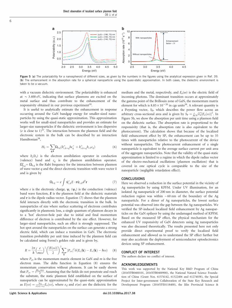
with a vacuum dielectric environment. The polarizability is enhancedat B 3.400 eV, indicating that surface plasmons are excited on themetal surface and thus contribute to the enhancement of theresponsivity obtained in our previous experiment18.It is useful to analytically estimate the enhancement in response
occurring around the GaN bandgap energy for smaller-sized nano-particles by using the quasi-static approximation. This approximationworks well for small-sized nanoparticles and provides an estimate forlarger-size nanoparticles if the dielectric environment is less dispersive(ε is close to 1)37. The interaction between the plasmon field and theelectronic system in the bulk can be described by an interactionHamiltonian38,
HI ¼Xq;k
Ok;qðbþc;kþqbcþq þ bþv;kþqbc;kcqÞ ð6Þ
where bc(bv) is the electron annihilation operator in conduction(valence) band and cq is the plasmon annihilation operator.O�
k;q¼ Ok;q is the Rabi frequency for the interaction between plasmonof wave vector q and the direct electronic transition with wave vector kand is given by
Ok;q ¼ e
Zc�c;kE � rcv;kd
3r ð7Þwhere e is the electronic charge, ψc (ψv) is the conduction (valence)band wave function, E is the plasmon field at the dielectric materialsand r is the dipole radius vector. Equation (7) shows that the plasmonfield interacts directly with the electronic transition in the bulk. Innanoparticles of size where surface scattering of electrons contributessignificantly in plasmonic loss, a single quantum of plasmon decays into a ‘hot’ electron–hole pair due to initial and final momentumdifference of electron is contributed by the size effect. However, forlarger-sized nanoparticles, such an effect is strongly suppressed. Thehot spot around the nanoparticles on the surface can generate a strongelectric field, which can induce a transition in GaN. The electronictransition probability per unit time induced by the plasmon field canbe calculated using Fermi’s golden rule and is given by,
R ¼ 2p_
e
mo
� �2 E oð Þj j2
� �2Xk
Pcvj j2d Ec kð Þ � Ev kð Þ � _oð Þ ð8Þ
where Pcv is the momentum matrix element in GaN and m is the freeelectron mass. The delta function in Equation (8) ensures themomentum conservation without phonons. It can be easily shownthat Pcv ¼ i
Ok;qmoE . Assuming that the fields do not penetrate and reach
the substrate, the static plasmon field established on the surface ofnanoparticle can be approximated by the quasi-static approximationas E oð Þ ¼ 3εd
ε oð ÞþεdEo oð Þ, where εd and ε(ω) are the dielectric for the
medium and the metal, respectively, and Eo(ω) is the electric field ofincoming photons. The dominant transition occurs at approximatelythe gamma point of the Brillouin zone of GaN, the momentum matrixelement for which is 8.85× 10− 20 in cgs units39. A relevant quantity isa Poynting vector, SP, which describes the power flow across anarbitrary cross-sectional area and is given by SP ¼ c
8pffiffiffiffiffiεd
pEo oð Þj j2. In
Figure 5b, we show the absorption per unit time using a plasmon fieldon the dielectric surface. The absorption rate is proportional to theresponsivity (that is, the absorption rate is also equivalent to thephotocurrent). The calculation shows that because of the localizedfield enhancement effect by SP, the enhancement can be up to 35times with nanoparticles relative to the photocurrent of the devicewithout nanoparticles. The photocurrent enhancement of a singlenanoparticle is equivalent to the average surface current per unit areaof the aggregate nanoparticles. Note that the validity of the quasi-staticapproximation is limited to a regime in which the dipole radius vectorof the electro-mechanical oscillations (plasmon oscillation) that iscovered in one optical cycle is comparable to the size of thenanoparticle (negligible retardation effect).
CONCLUSIONS
Here we observed a reduction in the surface potential in the vicinity ofAg nanoparticles by using KPFM. Under UV illumination, for anisolated Ag nanoparticle of 200 nm in diameter, the surface potentialreduction region was within ~ 60 nm of the boundary of the Agnanoparticle. For a dimer of Ag nanoparticles, the lowest surfacepotential was observed into the gap between the Ag nanoparticles. Weverified the SP-induced localized field enhancement by Ag nanopar-ticles on the GaN epilayer by using the undamaged method of KPFM.Based on the measured SP effect, the physical mechanism for theenhanced UV responsivity of GaN detectors using Ag nanoparticleswas also discussed theoretically. The results presented here not onlyprovide direct experimental proof to verify the localized fieldenhancement and allowed us to understand the SP effect further butmay also accelerate the deployment of semiconductor optoelectronicsdevices using SP enhancement.
CONFLICT OF INTERESTThe authors declare no conflict of interest.
ACKNOWLEDGEMENTS
This work was supported by the National Key R&D Program of China(2016YFB0400101, 2016YFB0400900), the National Natural Science Founda-tion of China (Grant Nos. 61574142, 61322406 and 61274038), the SpecialProject for Inter-government Collaboration of the State Key Research andDevelopment Program (2016YFE0118400), the Jilin Provincial Science &
2.5(a,b) = (180, 70) nm
With nanoparticles
Enhancementfactor ≈ 35
Without nanoparticles
(a,b) = (160, 70) nm(a,b) = (140, 70) nm
10
8
6
4
2
0
a b
2.0
1.5
1.0
0.5
2.0 2.5 3.0 3.5 4.0 4.5 5.0Energy (eV)
2.5 3.0 3.5 4.0 4.5Energy (eV)
Pol
ariz
abili
ty (
a.u.
)
Abs
orpt
ion
rate
(10
10 s
–1)
Figure 5 (a) The polarizability for a nanospheroid of different sizes, as given by the numbers in the figures using the analytical expression given in Ref. 39.(b) The enhancement in the absorption rate for a spherical nanoparticle using the quasi-static approximation. In both cases, the dielectric environment istaken to be a vacuum.
Direct observation of localized surface plasmon fieldDB Li et al
6
Light: Science & Applications doi:10.1038/lsa.2017.38

Technology Department (Grant No. 20150519001JH), the CAS Inter-disciplinary Innovation Team, and the Youth Innovation Promotion Associa-tion of CAS (Grant No. 2015171). For MIS's work, the support was provided bygrant No. DE-FG02-11ER46789 from the Materials Sciences and EngineeringDivision, Office of the Basic Energy Sciences, Office of Science, U.S. Depart-ment of Energy.
1 Hutter E, Fendler JH. Exploitation of localized surface plasmon resonance. Adv Mater2004; 16: 1685–1706.
2 Anker JN, Hall WP, Lyandres O, Shah NC, Zhao J et al. Biosensing with plasmonicnanosensors. Nat Mater 2008; 7: 442–453.
3 Mrejen M. Near-field imaging probes electromagnetic waves. Laser Focus World 2007;43: 28–32.
4 Challener WA, Peng CB, Itagi AV, Karns D, Peng W et al. Heat-assisted magneticrecording by a near-field transducer with efficient optical energy transfer. Nat Photon2009; 3: 220–224.
5 Nagatani N, Tanaka R, Yuhi T, Endo T, Kerman K et al. Gold nanoparticle-based novelenhancement method for the development of highly sensitive immunochromatographictest strips. Sci Technol Adv Mater 2006; 7: 270–275.
6 Gandra N, Portz C, Nergiz SZ, Fales A, Vo-Dinh T et al. Inherently stealthy and highlytumor-selective gold nanoraspberries for photothermal cancer therapy. Sci Rep 2015;5: 10311.
7 Bergman DJ, Stockman MI. Surface plasmon amplification by stimulated emission ofradiation: quantum generation of coherent surface plasmons in nanosystems. Phys RevLett 2003; 90: 027402.
8 Noginov MA, Zhu G, Belgrave AM, Bakker R, Shalaev VM et al. Demonstration of aspaser-based nanolaser. Nature 2009; 460: 1110–1112.
9 Apalkov V, Stockman MI. Proposed graphene nanospaser. Light Sci Appl 2014; 3:e191.
10 Su CY, Lin CH, Shih PY, Hsieh C, Yao YF et al. Coupling behaviors of surface plasmonpolariton and localized surface plasmon with an InGaN/GaN quantum well. Plasmonics2016; 11: 931–939.
11 Cho CY, Park SJ. Enhanced optical output and reduction of the quantum-confined Starkeffect in surface plasmon-enhanced green light-emitting diodes with gold nanoparticles.Opt Express 2016; 24: 7488–7494.
12 Lozano G, Rodriguez SRK, Verschuuren MA, Rivas JG. Metallic nanostructures forefficient LED lighting. Light Sci Appl 2016; 5: e16080.
13 Pryce IM, Koleske DD, Fischer AJ, Atwater HA. Plasmonic nanoparticle enhancedphotocurrent in GaN/InGaN/GaN quantum well solar cells. Appl Phys Lett 2010; 96:153501.
14 Atwater HA, Polman A. Plasmonics for improved photovoltaic devices. Nat Mater 2010;9: 205–213.
15 Su YH, Ke YF, Cai SL, Yao QY. Surface plasmon resonance of layer-by-layer goldnanoparticles induced photoelectric current in environmentally-friendly plasmon-sensi-tized solar cell. Light Sci Appl 2012; 1: e14.
16 Chen X, Jia BH, Zhang YN, Gu M. Exceeding the limit of plasmonic light trapping intextured screen-printed solar cells using Al nanoparticles and wrinkle-likegraphene sheets. Light Sci Appl 2013; 2: e92.
17 Lu JF, Xu CX, Dai J, Li JT, Wang YY et al. Improved UV photoresponse of ZnO nanorodarrays by resonant coupling with surface plasmons of Al nanoparticles. Nanoscale2015; 7: 3396–3403.
18 Li DB, Sun XJ, Song H, Li ZM, Chen YR et al. Realization of a high-performance GaNUV detector by nanoplasmonic enhancement. Adv Mater 2012; 24: 845–849.
19 Fan XF, Zheng WT, Singh DJ. Light scattering and surface plasmons on small sphericalparticles. Light Sci Appl 2014; 3: e179.
20 Yan F, Chen GN, Lu L, Spanier JE. Dynamics of photogenerated surface charge onBiFeO3 films. ACS Nano 2012; 6: 2353–2360.
21 Lan F, Li GY. Direct observation of hole transfer from semiconducting polymer to carbonnanotubes. Nano Lett 2013; 13: 2086–2091.
22 Liu Z, Xu K, Fan YM, Xu GZ, Huang ZW et al. Local ultra-violet surface photovoltagespectroscopy of single thread dislocations in gallium nitrides by Kelvin probe forcemicroscopy. Appl Phys Lett 2012; 101: 252107.
23 Barbet S, Aubry R, di Forte-Poisson MA, Jacquet JC, Deresmes D et al. Surfacepotential of n- and p-type GaN measured by Kelvin force microscopy. Appl Phys Lett2008; 93: 212107.
24 Nguyen A, Sharma P, Scott T, Preciado E, Klee V et al. Toward ferroelectric control ofmonolayer MoS2. Nano Lett 2015; 15: 3364–3369.
25 Wei JD, Neumann R, Wang X, Li SF, Fündling S et al. Polarity analysis of GaN nanorodsby photo-assisted Kelvin probe force microscopy. Phys Status Solidi C 2011;8: 2157–2159.
26 Wang R, Wang SN, Zhang DD, Li ZJ, Fang Y et al. Control of carrier type and density inexfoliated graphene by interface engineering. ACS Nano 2011; 5: 408–412.
27 Ryu SR, Ram SDG, Lee SJ, Cho HD, Lee S et al. Vertical current-flow enhancementvia fabrication of GaN nanorod p-n junction diode on graphene. Appl Surf Sci 2015;347: 793–798.
28 Nowak G, Weyher JL, Khachapuridze A, Grzegory I. Imaging extended non-homogeneities in HVPE grown GaN with Kelvin probe microscopy and photo-etching.J Cryst Growth 2012; 353: 68–71.
29 Kondratenko SV, Lysenko VS, Kozyrev YN, Kratzer M, Storozhuk DP et al. Local chargetrapping in Ge nanoclustersdetected by Kelvin probe force microscopy. Appl Surf Sci2016; 389: 783–789.
30 Oliver RA. Advances in AFM for the electrical characterization of semiconductors. RepProg Phys 2008; 71: 076501.
31 Melitz W, Shen J, Kummel AC, Lee S. Kelvin probe force microscopy and itsapplication. Surf Sci Rep 2011; 66: 1–27.
32 Rosenwaks Y, Shikler R, Glatzel T, Sadewasser S. Kelvin probe force microscopy ofsemiconductor surface defects. Phys Rev B 2004; 70: 085320.
33 Kronik L, Shapira Y. Surface photovoltage phenomena: theory, experiment, andapplications. Surf Sci Rep 1999; 37: 1–206.
34 Soudi A, Hsu CH, Gu Y. Diameter-dependent surface photovoltage and surface statedensity in single semiconductor nanowires. Nano Lett 2012; 12: 5111–5116.
35 Govorov AO, Zhang H, Gun’ko YK. Theory of photoinjection of hot plasmonic carriersfrom metal nanostructures into semiconductors and surface molecules. J. Phys. Chem C2013; 117: 16616.
36 Kuwata H, Tamaru H, Esumi K, Miyano K. Resonant light scattering from metalnanoparticles: Practical analysis beyond Rayleigh approximation. Appl Phys Lett 2003;83: 4625–4627.
37 Myroshnychenko V, Rodríguez-Fernández J, Pastoriza-Santos I, Funston AM, Novo Cet al. Modelling the optical response of gold nanoparticles. Chem Soc Rev 2008; 37:1792–1805.
38 Paudel HP, Apalkov V, Stockman MI. Three-dimensional topological insulator basednanospaser. Phys Rev B 2016; 93: 155105.
39 Shokhovets S, Gobsch G, Ambacher O. Momentum matrix element and conductionband nonparabolicity in wurtzite GaN. Appl Phys Lett 2005; 86: 161908.
This work is licensed under a Creative Commons Attribution 4.0International License. The images or other third party material in this
article are included in the article’s Creative Commons license, unless indicated otherwisein the credit line; if thematerial is not includedunder theCreativeCommons license, userswill need toobtainpermission fromthe licenseholder to reproduce thematerial.Toviewacopy of this license, visit http://creativecommons.org/licenses/by/4.0/
r The Author(s) 2017
Supplementary Information for this article can be found on the Light: Science & Applications’ website (http://www.nature.com/lsa).
Direct observation of localized surface plasmon fieldDB Li et al
7
Light: Science & Applicationsdoi:10.1038/lsa.2017.38


![Title Properties of electromagnetic wave propagation ... · modes contribute wave propagation along them [4] in a similar manner to localized surface plasmon in metallic photonic](https://img.dokumen.tips/doc/110x75/5f6c5c48041bbf414967cff1/title-properties-of-electromagnetic-wave-propagation-modes-contribute-wave-propagation.jpg)