Embed Size (px)
Citation preview

M
HCS500
Code Hopping Decoder
FEATURES
Security
• Encrypted storage of manufacturer’s code• Encrypted storage of encoder keys• Up to seven transmitters can be learned• KEELOQ code hopping technology• Normal and secure learning mechanisms
Operating
• 3.0V—5.5V operation• Internal oscillator• Auto bit rate detection
Other
• Stand-alone decoder chipset• External EEPROM for transmitter storage• Synchronous serial interface• 1 Kbit user EEPROM• 8-pin DIP/SOIC package
Typical Applications
• Automotive remote entry systems• Automotive alarm systems• Automotive immobilizers• Gate and garage openers• Electronic door locks• Identity tokens• Burglar alarm systems
Compatible Encoders
• HCS200, HCS300, HCS301, HCS360,HCS410 (PWM Mode)
DESCRIPTION
The Microchip Technology Inc. HCS500 is a code hop-ping decoder designed for secure Remote KeylessEntry (RKE) systems. The HCS500 utilizes the pat-ented KEELOQÒ code hopping system and high secu-rity learning mechanisms to make this a cannedsolution when used with the HCS encoders to imple-ment a unidirectional remote and access control sys-tems. The HCS500 can be used as a stand-alonedecoder or in conjunction with a microcontroller.
PACKAGE TYPE
BLOCK DIAGRAM
The manufacturer’s code, encoder keys, and synchro-nization information are stored in encrypted form inexternal EEPROM. The HCS500 uses the S_DAT andS_CLK inputs to communicate with a host controllerdevice.
The HCS500 operates over a wide voltage range of3.0 volts to 5.5 volts. The decoder employs automaticbit-rate detection, which allows it to compensate forwide variations in transmitter data rate. The decodercontains sophisticated error checking algorithms toensure only valid codes are accepted.
HC
S500
PDIP, SOIC
1
2
3
4
VDD
EE_CLK
EE_DAT
MCLR
8
7
6
5
VSS
RFIN
S_CLK
S_DAT
67-bit Reception Register
ExternalCONTROL
DECRYPTOR
RFIN
OSCILLATOR
S_DATS_CLK
MCLR
EEPROM
EE_DAT
EE_CLK
KEELOQ is a registered trademark of Microchip Technology, Inc.Microchip’s Secure Data Products are covered by some or all of the following patents:Code hopping encoder patents issued in Europe, U.S.A., and R.S.A. — U.S.A.: 5,517,187; Europe: 0459781; R.S.A.: ZA93/4726Secure learning patents issued in the U.S.A. and R.S.A. — U.S.A.: 5,686,904; R.S.A.: 95/5429
ã 1998 Microchip Technology Inc. Preliminary DS40153B-page 1

HCS500
1.0 KEELOQ SYSTEM OVERVIEW
1.1 Key Terms
• Manufacturer’s Code – A 64-bit word, unique to each manufacturer, used to produce a unique encoder key in each transmitter.
• Encoder Key – A 64-bit key, unique for each trans-mitter. The encoder key controls the KEELOQ decryption algorithm and is stored in EEPROM on the decoder device.
• Learn – The receiver uses information that is transmitted to derive the transmitter’s encoder key, decrypt the discrimination value, and the syn-chronization counter in learning mode. The encoder key is a function of the manufacturer’s code and the device serial number and/or seed value.
The HCS encoders and decoders employ the KEELOQ
code hopping technology and a KEELOQ encryptionalgorithm to achieve a high level of security. Codehopping is a method by which the code transmittedfrom the transmitter to the receiver is different everytime a button is pushed. This method, coupled with atransmission length of 66 bits, virtually eliminates theuse of code ‘grabbing’ or code ‘scanning’.
1.2 HCS Encoder Overview
The HCS encoders have a small EEPROM array whichmust be loaded with several parameters before use.The most important of these values are:
• An encoder key that is generated at the time of production
• A 16-bit synchronization counter value• A 28-bit serial number which is meant to be
unique for every encoder
The manufacturer programs the serial number for eachencoder at the time of production, while the ‘Key Gen-eration Algorithm’ generates the encoder key(Figure 1-1). Inputs to the key generation algorithm typ-ically consist of the encoder’s serial number and a64-bit manufacturer’s code, which the manufacturercreates.
FIGURE 1-1: CREATION AND STORAGE OF ENCRYPTION KEY DURING PRODUCTION
Note: The manufacturer code is a pivotal part ofthe system’s overall security. Conse-quently, all possible precautions must betaken and maintained for this code.
Transmitter
Manufacturer’s
Serial Number or
Code
Encryption Key
KeyGenerationAlgorithm
Serial NumberEncryption KeySync Counter
.
.
.
HCS500 EEPROM Array
Seed
DS40153B-page 2 Preliminary ã 1998 Microchip Technology Inc.

HCS500
The 16-bit synchronization counter is the basis for thetransmitted code changing for each transmission and isupdated each time a button is pressed. Because of thecomplexity of the KEELOQ encryption algorithm, achange in one bit of the synchronization counter valuewill result in a large change in the actual transmittedcode. There is a relationship (Figure 1-2) between theencoder key values in EEPROM and how they are usedin the encoder. Once the encoder detects that a buttonhas been pressed, the encoder reads the button andupdates the synchronization counter. The synchroniza-tion value is then combined with the encoder key in theKEELOQ encryption algorithm, and the output is 32 bitsof encrypted information. This data will change withevery button press, hence, it is referred to as the codehopping portion of the code word. The 32-bit code hop-ping portion is combined with the button informationand the serial number to form the code word transmit-ted to the receiver.
1.3 HCS Decoder Overview
Before a transmitter and receiver can work together,the receiver must first ‘learn’ and store certain informa-tion from the transmitter. This information includes a‘check value’ of the serial number, the encoder key, andcurrent synchronization counter value.
When a validly formatted message is detected, thereceiver first compares the serial number. If the serialnumber check value is from a learned transmitter, themessage is decrypted. Next, the receiver checks thedecrypted synchronization counter value against whatis stored in memory. If the synchronization countervalue is verified, then a valid transmission message issent. Figure 1-3 shows the relationship between someof the values stored by the receiver and the valuesreceived from the transmitter.
FIGURE 1-2: BASIC OPERATION OF A CODE HOPPING TRANSMITTER (ENCODER)
FIGURE 1-3: BASIC OPERATION OF A CODE HOPPING RECEIVER (DECODER)
KEELOQ
Algorithm
Button PressInformationEncryption
EEPROM Array
32 Bits of Encrypted Data Serial Number
Transmitted Information
Encoder Key
Sync. Counter Value
Serial Number
Button PressInformation
EEPROM Array
Encoder Key
32 Bits of Encrypted DataSerial Number
Received Information
DecryptedSynchronization Counter
Check forMatch
Check forMatch
KEELOQ
AlgorithmDecryption
Sync. Counter Value
Serial Number
Manufacturer Code
ã 1998 Microchip Technology Inc. Preliminary DS40153B-page 3

HCS500
2.0 PIN ASSIGNMENT
PINDecoderFunction I/O(1)
Buffer
Type(1) Description
1 VDD P — Power Connection
2 EE_CLK O TTL Clock to I2C™ EEPROM
3 EE_DAT I/O TTL Data to I2C EEPROM
4 MCLR I ST Master clear input
5 S_DAT I/O TTL Synchronous data from controller
6 S_CLK I TTL Synchronous clock from controller
7 RFIN I TTL RF input from receiver
8 GND P — Ground connection
Note: P = power, I = in, O = out, and ST = Schmitt Trigger input.
I2C is a trademark of Philips Corporation.
DS40153B-page 4 Preliminary ã 1998 Microchip Technology Inc.

HCS500
3.0 DECODER OPERATION
3.1 Learning a Transmitter to a Receiver (Normal or Secure Learn)
Before the transmitter and receiver can work together,the receiver must first ‘learn’ and store the followinginformation from the transmitter in EEPROM:
• A check value of the serial number• The encoder key• The current synchronization counter value
The decoder must also store the manufacturer’s code(Section 1.2) in protected memory. This code willtypically be the same for all of the decoders in a sys-tem.
The HCS500 has seven memory slots, and, conse-quently, can store up to seven transmitters. During thelearn procedure, the decoder searches for an emptymemory slot for storing the transmitter’s information.When all of the memory slots are full, the decoder willoverwrite the last transmitter’s information. To erase allof the memory slots at once, use the ERASE_ALLcommand (C3H).
3.1.1 LEARNING PROCEDURE
Learning is initiated by sending the ACTIVATE_LEARN(D2H) command to the decoder. The decoder acknowl-edges reception of the command by pulling the dataline high.
For the HCS500 decoder to learn a new transmitter, thefollowing sequence is required:
1. Activate the transmitter once.2. Activate the transmitter a second time. (In
secure learning mode, the seed transmissionmust be transmitted during the second stage oflearn by activating the appropriate buttons onthe transmitter.) The HCS500 will transmit a learn-status string,indicating that the learn was successful.
3. The decoder has now learned the transmitter.4. Repeat steps 1-3 to learn up to seven
transmitters
Note 1: Learning will be terminated if twononsequential codes were received or if twoacceptable codes were not decoded within30 seconds.
2: If more than seven transmitters are learned,the new transmitter will replace the lasttransmitter learned. It is, therefore, not pos-sible to erase lost transmitters byrepeatedly learning new transmitters. Toremove lost or stolen transmitters,ERASE_ALL transmitters and relearn allavailable transmitters.
3: Learning a transmitter with an encoder keythat is identical to a transmitter already inmemory replaces the existing transmitter. Inpractice, this means that all transmittersshould have unique encoder keys. Learninga previously learned transmitter does notuse any additional memory slots.
The following checks are performed by the decoder todetermine if the transmission is valid during learn:
• The first code word is checked for bit integrity. • The second code word is checked for bit integrity. • The encoder key is generated according to the
selected algorithm.• The hopping code is decrypted.• The discrimination value is checked.• If all the checks pass, the key, serial number
check value, and synchronization counter values are stored in EEPROM memory.
Figure 3-1 shows a flow chart of the learn sequence.
FIGURE 3-1: LEARN SEQUENCE
Enter LearnMode
Wait for Receptionof Second
Compare DiscriminationValue with Serial Number
Use Generated Key to Decrypt
Equal?
Sync. counter valueEncoder key
Exit
Learn successful. Store: LearnUnsuccessful
No
Yes
Wait for Receptionof a Valid Code
Non-Repeated Valid Code
Generate Keyfrom Serial Number/
Seed Value
Serial number check value
ã 1998 Microchip Technology Inc. Preliminary DS40153B-page 5

HCS500
3.2 Validation of Codes
The decoder waits for a transmission and checks theserial number to determine if it is a learned transmitter.If it is, it takes the code hopping portion of the transmis-sion and decrypts it, using the encoder key. It uses thediscrimination value to determine if the decryption wasvalid. If everything up to this point is valid, thesynchronization counter value is evaluated.
3.3 Validation Steps
Validation consists of the following steps:
1. Search EEPROM to find the Serial NumberCheck Value Match
2. Decrypt the Hopping Code3. Compare the 10 bits of the discrimination value
with the lower 10 bits of serial number4. Check if the synchronization counter value falls
within the first synchronization window.5. Check if the synchronization counter value falls
within the second synchronization window.6. If a valid transmission is found, update the
synchronization counter, else use the nexttransmitter block, and repeat the tests.
FIGURE 3-2: DECODER OPERATION
3.4 Synchronization with Decoder
The KEELOQ technology features a sophisticatedsynchronization technique (Figure 3-3) which does notrequire the calculation and storage of future codes. Ifthe stored synchronization counter value for thatparticular transmitter and the synchronization countervalue that was just decrypted are within a formattedwindow of 16, the counter is stored, and the commandis executed. If the synchronization counter value wasnot within the single operation window, but is within thedouble operation window of the 16K window, thetransmitted synchronization counter value is stored in atemporary location, and the decoder goes back to wait-ing for another transmission. When the next validtransmission is received, it will check the newsynchronization counter value with the one in tempo-rary storage. If the two values are sequential, it isassumed that the counter had just gotten out of thesingle operation ‘window’, but is now back in synchroni-zation, so the new synchronization counter value isstored, and the command is executed. If a transmitterhas somehow gotten out of the double operationwindow, the transmitter will not work and must berelearned. Since the entire window rotates after eachvalid transmission, codes that have been used becomepart of the ‘blocked’ (48K) codes and are no longervalid. This eliminates the possibility of grabbing a previ-ous code and retransmitting to gain entry.
FIGURE 3-3: SYNCHRONIZATION WINDOWTransmission
Received?
DoesSer # Check Val
Match?
Decrypt Transmission
Isdecryption
valid?
Iscounter within
16?
Iscounter within
16K?
UpdateCounter
ExecuteCommand
Save Counterin Temp Location
Start
No
No
No
No
Yes
Yes
Yes
Yes
Yes
No
and
Blocked
Entire Window rotates to eliminateuse of previouslyused codes
CurrentPosition
(48K Codes)
DoubleOperation(16K Codes)
SingleOperationWindow(16 Codes)
DS40153B-page 6 Preliminary ã 1998 Microchip Technology Inc.

HCS500
4.0 INTERFACING TO A MICROCONTROLLER
The HCS500 interfaces to a microcontroller via a syn-chronous serial interface. A clock and data line areused to communicate with the HCS500. The microcon-troller controls the clock line. There are two groups ofdata transfer messages. The first is from the decoderwhenever the decoder receives a valid transmission.The decoder signals reception of a valid code by takingthe data line high (maximum of 500 ms) The microcon-troller then services the request by clocking out a datastring from the decoder. The data string contains thefunction code, the status bit, and block indicators. Thesecond is from the controlling microcontroller to thedecoder in the form of a defined command set.
Figure 4-1 shows the HCS500 decoder and the I/Ointerface lines necessary to interface to a microcontrol-ler.
4.1 Valid Transmission Message
The decoder informs the microcontroller of a validtransmission by taking the data line high for up to500 ms. The controlling microcontroller must acknowl-edge by taking the clock line high. The decoder thentakes the data line low. The microcontroller can thenbegin clocking a data stream out of the HCS500. Thedata stream consists of:
• Start bit ‘0’.• 2 status bits [REPEAT, VLOW]. • 4-bit function code [S3 S2 S1 S0].• Stop bit ‘1’. • 4 bits indicating which block was used
[TX3…TX0].• 4 bits indicating the number of transmitters
learned into the decoder [CNT3…CNT0].• 64 bits of the received transmission with the hop-
ping code decrypted.
The decoder will terminate the transmission of the datastream at any point where the clock is kept low forlonger than 1 ms.Therefore, the microcontroller canonly clock out the required bits. A maximum of 80 bitscan be clocked out of the decoder.
FIGURE 4-1: HCS500 DECODER AND I/O INTERFACE LINES
FIGURE 4-2: DECODER VALID TRANSMISSION MESSAGE
Note: Data is always clocked in/out LeastSignificant Bit (LSB) first.
A0
A1
A2
Vss
24LC02
Vcc
WP
SCL
SD
1
2
3
4
8
7
6
5
VDD
EE_CLK
EE_DAT
MCLR
Vss
RFIN
S_CLK
S_DAT
1
2
3
4
8
7
6
5
VDDRF RECEIVER
SYNC CLOCK
SYNC DATA
MICRO RESETHCS500
1K
Decoder Signal Valid
TCLKH TDS
A B Cii
TPP3
TDHI
TCLA
Received String
Ci
S_DAT TX0 TX3 RX63REPT VLOW S0 S1 S2 S3 CNT0 CNT30 RX0 RX1 RX621
S_CLK
Information
TPP1
TCLKH
TCLKL
Transmission
ã 1998 Microchip Technology Inc. Preliminary DS40153B-page 7

HCS500
4.2 Command Mode
4.2.1 MICROCONTROLLER COMMAND MODE ACTIVATION
The microcontroller command consists of four parts.The first part activates the command mode, the secondpart is the actual command, the third is the addressaccessed, and the last part is the data. The microcon-troller starts the command by taking the clock line highfor up to 500 ms. The decoder acknowledges the start-up sequence by taking the data line high. The micro-controller takes the clock line low, after which thedecoder will take the data line low, tri-state the data lineand wait for the command to be clock in. The data mustbe set up on the rising edge and will be sampled on thefalling edge of the clock line.
4.2.2 COLLISION DETECTION
The HCS500 uses collision detection to preventclashes between the decoder and microcontroller.Whenever the decoder receives a valid transmissionthe following sequence is followed:
• The decoder first checks to see if the clock line is high. If the clock line is high, the valid transmis-sion notification is aborted, and the microcontrol-ler command mode request is serviced.
• The decoder takes the data line high and checks that the clock line doesn’t go high within 50 ms. If the clock line goes high, the valid transmission notification is aborted and the command mode request is serviced.
• If the clock line goes high after 50 ms but before 500 ms, the decoder will acknowledge by taking the data line low.
• The microcontroller can then start to clock out the 80-bit data stream of the received transmission.
FIGURE 4-3: MICROCONTROLLER COMMAND MODE ACTIVATION
MSB
A
Command ByteStart Command
TCLKL
TCLKH TDS
B C
LSB
TSTART
TCMD
D
TDATA
E
Address Byte Data Byte
TADDR
TREQ
TRESP
CLK
mC Data
HCS500Data
MSBLSB MSBLSB
TACK
DS40153B-page 8 Preliminary ã 1998 Microchip Technology Inc.

HCS500
4.2.3 COMMAND ACTIVATION TIMES
The command activation time (Table 4-1) is defined asthe maximum time the microcontroller has to wait for aresponse from the decoder. The decoder will abort andservice the command request. The response timedepends on the state of the decoder when the com-mand mode is requested.
4.2.4 DECODER COMMANDS
The command byte specifies the operation required bythe controlling microcontroller. Table 4-2 lists the com-mands.
TABLE 4-1: COMMAND ACTIVATION TIMES
Decoder State Min Max
While receiving transmissions — 2 1/2 BPWMAX = 2.7 ms
During the validation of a received transmission — 3 ms
During the update of the sync counters — 40 ms
During learn — 170 ms
TABLE 4-2: DECODER COMMANDS
Instruction Command Byte Operation
READ F016 Read a byte from user EEPROM
WRITE E116 Write a byte to user EEPROM
ACTIVATE_LRN D216 Activate a learn sequence on the decoder
ERASE_ALL C316 Activate an erase all function on the decoder
PROGRAM B416 Program manufacturer’s code and configuration byte
ã 1998 Microchip Technology Inc. Preliminary DS40153B-page 9

HCS500
4.2.5 READ BYTE/S FROM USER EEPROM
The read command (Figure 4-4) is used to read bytesfrom the user EEPROM. The offset in the userEEPROM is specified by the address byte which istruncated to seven bits (C to D). After the address, adummy byte must be clocked in (D to E). The EEPROMdata byte is clocked out on the next rising edge of theclock line with the least significant bit first (E to F).Sequential reads are possible by repeating sequence Eto F within 1 ms after the falling edge of the previousbyte’s Most Significant Bit (MSB) bit. During thesequential read, the address value will wrap after 128bytes. The decoder will terminate the read command ifno clock pulses are received for a period longer than1.2 ms.
4.2.6 WRITE BYTE/S TO USER EEPROM
The write command (Figure 4-5) is used to write a loca-tion in the user EEPROM. The address byte is trun-cated to seven bits (C to D). The data is clocked in leastsignificant bit first. The clock line must be asserted toinitiate the write. Sequential writes of bytes are possibleby clocking in the byte and then asserting the clock line(D – F). The decoder will terminate the write commandif no clock pulses are received for a period longer than1.2 ms After a successful write sequence the decoderwill acknowledge by taking the data line high and keep-ing it high until the clock line goes low.
FIGURE 4-4: READ BYTES FROM USER EEPROM
FIGURE 4-5: WRITE BYTES TO USER EEPROM
Decoder DATA
MSB
A
Command ByteStart Command
B C
LSB
D
TRD
E
Address Byte Dummy Byte
CLK
mC DATA
F
Data Byte
MSBLSB MSBLSB
MSBLSB
TRD
Decoder DATA
MSB
A
Command ByteStart Command
B C
LSB
D
TWR
E
Address Byte Data Byte
CLK
mC DATA
F
Acknowledge
MSBLSB MSBLSB
TACK
TRESP
TACK2
DS40153B-page 10 Preliminary ã 1998 Microchip Technology Inc.
HCS500
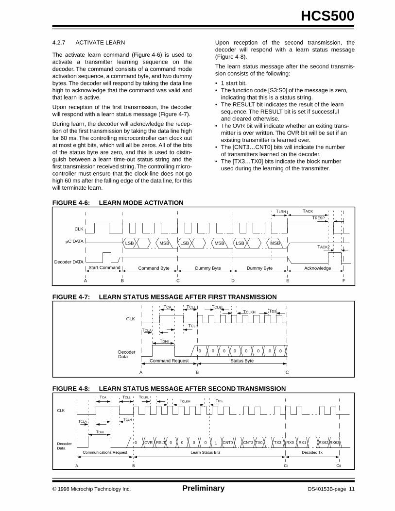
4.2.7 ACTIVATE LEARN
The activate learn command (Figure 4-6) is used toactivate a transmitter learning sequence on thedecoder. The command consists of a command modeactivation sequence, a command byte, and two dummybytes. The decoder will respond by taking the data linehigh to acknowledge that the command was valid andthat learn is active.
Upon reception of the first transmission, the decoderwill respond with a learn status message (Figure 4-7).
During learn, the decoder will acknowledge the recep-tion of the first transmission by taking the data line highfor 60 ms. The controlling microcontroller can clock outat most eight bits, which will all be zeros. All of the bitsof the status byte are zero, and this is used to distin-guish between a learn time-out status string and thefirst transmission received string. The controlling micro-controller must ensure that the clock line does not gohigh 60 ms after the falling edge of the data line, for thiswill terminate learn.
Upon reception of the second transmission, thedecoder will respond with a learn status message(Figure 4-8).
The learn status message after the second transmis-sion consists of the following:
• 1 start bit.• The function code [S3:S0] of the message is zero,
indicating that this is a status string. • The RESULT bit indicates the result of the learn
sequence. The RESULT bit is set if successful and cleared otherwise.
• The OVR bit will indicate whether an exiting trans-mitter is over written. The OVR bit will be set if an existing transmitter is learned over.
• The [CNT3…CNT0] bits will indicate the number of transmitters learned on the decoder.
• The [TX3…TX0] bits indicate the block number used during the learning of the transmitter.
FIGURE 4-6: LEARN MODE ACTIVATION
FIGURE 4-7: LEARN STATUS MESSAGE AFTER FIRST TRANSMISSION
FIGURE 4-8: LEARN STATUS MESSAGE AFTER SECOND TRANSMISSION
Decoder DATA
MSB
A
Command ByteStart Command
B C
LSB
D
TLRN
E
Dummy Byte Dummy Byte
CLK
mC DATA
F
Acknowledge
MSBLSB MSBLSB
TACK
TRESP
TACK2
Command Request
TCLKLTCLKH
TCATDS
A B
TCLL
TDHI
TCLATCLH
CLK
Decoder 0 0 0 0 0 00 0
Status Byte
C
Data
Communications Request
TCLKLTCLKH
TCATDS
A B Cii
TCLL
TDHI
TCLATCLH
CLK
Decoder TX0 TX3 RX63OVR RSLT 0 0 0 0 CNT0 CNT30 RX0 RX1 RX621
Ci
Learn Status Bits Decoded TxData
ã 1998 Microchip Technology Inc. Preliminary DS40153B-page 11

HCS500
4.2.8 ERASE ALL
The erase all command (Figure 4-9) erases all thetransmitters in the decoder. After the command and twodummy bytes are clocked in, the clock line must beasserted to activate the command. After a successfulcompletion of an erase all command, the data line isasserted until the clock line goes low.
4.3 Stand-alone Mode
The HCS500 decoder can also be used in stand-aloneapplications. The HCS500 will activate the data line forup to 500 ms if a valid transmission was received, andthis output can be used to drive a relay circuit. To acti-vate learn or erase all commands, a button must beconnected to the CLK input. User feedback is indicatedon an LED connected to the DATA output line. If theCLK line is pulled high, using the learn button, the LEDwill switch on. After the CLK line is kept high for longerthan 2 seconds, the decoder will switch the LED line off,indicating that learn will be entered if the button isreleased. If the CLK line is kept high for another 6 sec-onds, the decoder will activate an ERASE_ALL Com-mand.
Learn mode can be aborted by taking the clock linehigh until the data line goes high (LED switches on).During learn, the data line will give feedback to the userand, therefore, must not be connected to the relay drivecircuitry.
After taking the clock low and before a transmitter islearn, any low-to-high change on the clock line may ter-minate learn. This has learn implications when a switchwith contact bounce is used.
4.4 Erase All Command and Erase Command
The Table 4-3 describes two versions of the Erase Allcommand.
Subcommand 01 can be used where a transmitter withpermanent status is implemented in the microcontrollersoftware. Use of subcommand 01 ensures that the per-manent transmitter remains in memory even when allother transmitters are erased. The first transmitterlearned after any of the following events is the firsttransmitter in memory and becomes the permanenttransmitter:
1. Programming of the manufacturer’s code.2. Erasing of all transmitters
(subcommand 00 only).
4.5 Test mode
A special test mode is activated after:
1. Programming of the manufacturer’s code.2. Erasing of all transmitters.
Test mode can be used to test a decoder before anytransmitters are learned on it. Test mode enables test-ing of decoders without spending the time to learn atransmitter. Test mode is terminated after the first suc-cessful learning of an ordinary transmitter. In testmode, the decoder responds to a test transmitter. Thetest transmitter has the following properties:
1. Encoder key = manufacturer’s code.2. Serial number = any value.3. Discrimination bits = lower 10 bits of the serial
number.4. Synchronization counter value = any value
(synchronization information is ignored).
Because the synchronization counter value is ignoredin test mode, any number of test transmitters can beused, even if their synchronization counter values aredifferent.
4.6 Power Supply Supervisor
Reliable operation of the HCS500 requires that thecontents of the EEPROM memory be protected againsterroneous writes. To ensure that erroneous writes donot occur after supply voltage “brown-out” conditions,the use of a proper power supply supervisor device isimperative (Figure 4-10 and Figure 8-2).
Note: The REPS bit must be cleared in the con-figuration byte in stand-alone mode.
TABLE 4-3: ERASE ALL COMMAND
Command Byte
Subcommand Byte
Description
C316 0016Erase all transmitters.
C316 0116
Erase all transmit-ters except 1. The first transmitter in memory is not erased.
DS40153B-page 12 Preliminary ã 1998 Microchip Technology Inc.

HCS500
FIGURE 4-9: ERASE ALL
FIGURE 4-10: STAND-ALONE MODE LEARN/ERASE-ALL TIMING
FIGURE 4-11: TYPICAL STAND-ALONE APPLICATION CIRCUIT
Decoder DATA
MSB
A
Command ByteStart Command
B C
LSB
D
TERA
E
Subcommand Byte Dummy Byte
CLK
mC DATA
F
Acknowledge
MSBLSB MSBLSB
TACK
TRESP
TACK2
DATA
A
Erase-All Activation
TPP1 TPP2
CLK
B C D
Learn Activation
TPP3
Successful
E
TPP4
OUTPUT
K1
RELAY SPST
VccVcc
S1LEARN
VCC
1K
A01A12
A23VSS4 SDA 5SCL 6WP 7VCC 8U2
24LC02B
VDD1
EECLK2EEDAT3MCLR4 SDAT 5SCLK 6RFIN 7VSS
8U1
HCS500
Q1NPN
R1
10K
D1LED
R210K
R310K
VCC
VI GND
VO
U3POWER SUPPLY
XXX
RFReceiver
SUPERVISOR 4.5V
22 mF
Note: Because each HCS500 is individually matched to its EEPROM, in-circuit programming isstrongly recommended.
In-circuit ProgrammingProbe Pads
ã 1998 Microchip Technology Inc. Preliminary DS40153B-page 13

HCS500
5.0 DECODER PROGRAMMINGThe decoder uses a 2K, 24LC02B serial EEPROM. The memory is divided between system memory that stores thetransmitter information (read protected) and user memory (read/write). Commands to access the user memory aredescribed in Sections 4.2.5 and 4.2.6.
The following information stored in system memory needs to be programmed before the decoder can be used:
• 64-bit manufacturer’s code• Decoder configuration byte
5.1 Configuration Byte
The decoder is configured during initialization by setting the appropriate bits in the configuration byte. The following tablelist the options:
5.1.1 LRN_MODE
LRN_MODE selects between two learning modes. With LRN_MODE = 0, the normal (serial number derived) mode isselected; with LRN_MODE=1, the secure (seed derived) mode is selected. See Section 6.0 for more detail on learningmodes.
5.1.2 LRN_ALG
LRN_ALG selects between the two available algorithms. With LRN_ALG = 0, is selected the KEELOQ decryptionalgorithm is selected; with LRN_ALG = 1, the XOR algorithm is selected. See Section 6.0 for more detail on learningalgorithms.
5.1.3 REPEAT
The HCS500 can be configured to indicate repeated transmissions. In a stand-alone configuration, repeated transmis-sions must be disabled.
Note 1: These memory locations are read protected and can only be written to using the program command withthe device powered up.
2: The contents of the system memory is encrypted by a unique 64-bit key that is stored in the HCS500. Toinitialize the system memory, the HCS500’s program command must be used. The EEPROM and HCS500are matched, and the devices must be kept together. In-circuit programming is therefore recommended.
Bit Mnemonic Description
0 LRN_MODE Learning mode selection LRN_MODE = 0—Normal Learn LRN_MODE = 1—Secure Learn
1 LRN_ALG Algorithm selection LRN_ALG = 0—KEELOQ Decryption AlgorithmLRN_ALG = 1—XOR Algorithm
2 REPEAT Repeat Transmission enable0 = Disable1 = Enabled
3 Not Used Reserved4 Not Used Reserved5 Not Used Reserved6 Not Used Reserved7 Not Used Reserved
DS40153B-page 14 Preliminary ã 1998 Microchip Technology Inc.

HCS500
5.2 Programming Waveform
The programming command consists of the following:
• Command Request Sequence (A to B)• Command Byte (B to C)• Configuration Byte (C to D)• Manufacturer’s Code Eight Data Bytes (D to G)• Activation and Acknowledge Sequence (G to H)
5.3 Programming Data String
A total of 80 bits are clocked into the decoder. The 8-bitcommand byte is clocked in first, followed by the 8-bitconfiguration byte and the 64-bit manufacturer’s code.The data must be clocked in Least Significant Bit (LSB)first. The decoder will then encrypt the manufacturer’scode using the decoder’s unique 64-bit EEPROMencoder key. After completion of the programmingEEPROM, the decoder will acknowledge by taking thedata line high (G to H). If the data line goes high within30 ms after the clock goes high, programming alsofails.
FIGURE 5-1: PROGRAMMING WAVEFORM
DECODER DATA
MSB MSB
A
Command ByteStart Command
TCLKL
TCLKHTPP1 TDS
B C
LSB
TPP3
TPP2
TCMD
D
LSB LSB
Configuration Byte
CLK
mC DATA MSB
TDATA
G
Most Significant Byte
H
TACK
TWT2
TAW
Acknowledge
MSB
E
Least Significant Byte
F
TDATATADDR
TPP4
ã 1998 Microchip Technology Inc. Preliminary DS40153B-page 15

HCS500
6.0 KEY GENERATIONThe HCS500 supports three learning schemes which are selected during the initialization of the system EEPROM. Thelearning schemes are:
• Normal learn using the KEELOQ decryption algorithm• Secure learn using the KEELOQ decryption algorithm• Secure learn using the XOR algorithm
6.1 Normal (Serial Number derived) Learn using the KEELOQ Decryption Algorithm
This learning scheme uses the KEELOQ decryption algorithm and the 28-bit serial number of the transmitter to derivethe encoder key. The 28-bit serial number is patched with predefined values as indicated below to form two 32-bit seeds.
SourceH = 60000000 00000000H + Serial Number | 28 BitsSourceL = 20000000 00000000H + Serial Number | 28 Bits
Then, using the KEELOQ decryption algorithm and the manufacturer’s code the encoder key is derived as fol-lows:
KeyH Upper 32 bits = F KEELOQ Decryption (SourceH) | 64-Bit Manufacturer’s CodeKeyL Lower 32 bits = F KEELOQ Decryption (SourceL) | 64-Bit Manufacturer’s Code
6.2 Secure (Seed Derived) Learn using the KEELOQ Decryption Algorithm
This scheme uses the secure seed transmitted by the encoder to derive the two input seeds. The decoder always usesthe lower 64 bits of the transmission to form a 60-bit seed. The upper 4 bits are always forced to zero.
For 32-bit seed encoders (HCS200/HCS300/HCS301):
SourceH = Serial Number Lower 28 bits SourceL = Seed 32 bits
For 48-bit seed encoders (HCS360/HCS361):
SourceH = Seed Upper 16 bits + Serial Number Upper 16 bits with upper 4 bits set to zeroSourceL = Seed Lower 32 bits
For 60-bit seed encoders (HCS410):
SourceH = Seed Upper 32 bits with upper 4 bits set to zeroSourceL = Seed Lower 32 bits
The KEELOQ decryption algorithm and the manufacturer’s code is used to derive the encoder key as follows:
KeyH Upper 32 bits = F KEELOQ Decrypt (SourceH) | 64 Bit Manufacturer’s CodeKeyL Lower 32 bits = F KEELOQ Decrypt (SourceL) | 64 Bit Manufacturer’s Code
6.3 Secure (Seed Derived) Learn using the XOR Algorithm
This scheme uses the seed transmitted by the encoder to derive the two input seeds. The decoder always use the lower64 bits of the transmission to form a 60-bit seed. The upper 4 bits are always forced to zero.
For 32-bit seed encoders (HCS200/HCS300/HCS301):
SourceH = Serial Number Lower 28 bits SourceL = Seed 32 bits
For 48-bit seed encoders (HCS360/HCS361):
SourceH = Seed Upper 16 bits + Serial Number Upper 16 bits with upper 4 bits set to zeroSourceL = Seed Lower 32 bits
For 60-bit seed encoders (HCS410):
SourceH = Seed Upper 32 bits with upper 4 bits set to zeroSourceL = Seed Lower 32 bits
Then, using the KEELOQ decryption algorithm and the manufacturer’s code the encoder key is derivedas follows:
KeyH Upper 32 bits = SourceH XOR 64-Bit Manufacturer’s Code | Upper 32 bitsKeyL Lower 32 bits = SourceL XOR 64-Bit Manufacturer’s Code | Lower 32 bits
DS40153B-page 16 Preliminary ã 1998 Microchip Technology Inc.

HCS500
7.0 KEELOQ ENCODERS
7.1 Transmission Format (PWM)
The KEELOQ encoder transmission is made up of sev-eral parts (Figure 7-1). Each transmission begins witha preamble and a header, followed by the encryptedand then the fixed data. The actual data is 66/67 bitswhich consists of 32 bits of encrypted data and 34/35bits of non-encrypted data. Each transmission is fol-lowed by a guard period before another transmissioncan begin. The code hopping portion provides up tofour billion changing code combinations and includesthe button status bits (based on which buttons wereactivated), along with the synchronization countervalue and some discrimination bits. The non-code hop-ping portion is comprised of the status bits, the functionbits, and the 28-bit serial number. The encrypted andnon-encrypted combined sections increase the num-ber of combinations to 7.38 x 10¹⁹.
7.2 Code Word Organization
The HCS encoder transmits a 66/67-bit code wordwhen a button is pressed. The 66/67-bit word is con-structed from a code hopping portion and a non-codehopping portion (Figure 7-2).
The Encrypted Data is generated from four button bits,two overflow counter bits, ten discrimination bits, andthe 16-bit synchronization counter value.
The Non-encrypted Data is made up from 2 statusbits, 4 function bits, and the 28/32-bit serial number.
FIGURE 7-1: CODE WORD TRANSMISSION FORMAT
FIGURE 7-2: CODE WORD ORGANIZATION
LOGIC ‘0’
LOGIC ‘1’
BitPeriod
Preamble HeaderCode Hopping Portion
of TransmissionFixed Portion ofTransmission
Guard Time
TP TH THOP TFIX TG
RepeatVLOW (1 bit)
Button StatusS2S1S0S3
(4 bits)
28-bit Serial
Number
Button StatusS2S1S0S3
(4 bits)
Discrimination bits (12 bits)
16-bitSync.
Counter Value
CRC1* CRC0*
3/2 bits+ Serial Number and
Button Status (32 bits)+ 32 bits of Encrypted Data
Encrypted DataNon-encrypted Data
*HCS360/361
66/67 bitsof DataTransmitted
ã 1998 Microchip Technology Inc. Preliminary DS40153B-page 17

HCS500
8.0 ELECTRICAL CHARACTERISTICS FOR HCS500Absolute Maximum Ratings†
Ambient temperature under bias .............................................................................................................. -40°C to +85°C
Storage temperature ..............................................................................................................................-65 °C to +150°C
Voltage on any pin with respect to VSS (except VDD) ........................................................................ -0.6V to VDD +0.6V
Voltage on VDD with respect to Vss.................................................................................................................. 0 to +7.0V
Total power dissipation (Note) ............................................................................................................................. 700 mW
Maximum current out of VSS pin........................................................................................................................... 200 mA
Maximum current into VDD pin ............................................................................................................................. 150 mA
Input clamp current, IIK (VI < 0 or VI > VDD) ........................................................................................................ ± 20 mA
Output clamp current, IOK (VO < 0 or VO >VDD) ................................................................................................. ± 20 mA
Maximum output current sunk by any I/O pin......................................................................................................... 25 mA
Maximum output current sourced by any I/O pin.................................................................................................... 25 mA
Note: Power dissipation is calculated as follows: PDIS = VDD x {IDD - å IOH} + å {(VDD–VOH) x IOH} + å(VOl x IOL)
† NOTICE: Stresses above those listed under “Absolute Maximum Ratings” may cause permanent damage to the device. This is a stress rating only and functional operation of the device at those or any other conditions above those indicated in the operation listings of this specification is not implied. Exposure to maximum rating conditions for extended periods may affect device reliability.
DS40153B-page 18 Preliminary ã 1998 Microchip Technology Inc.

HCS500
FIGURE 8-1: RESET WATCHDOG TIMER, OSCILLATOR START-UP TIMER AND POWER-UP TIMER TIMING
TABLE 8-1: DC CHARACTERISTICS
Standard Operating Conditions (unless otherwise stated)Operating temperatureCommercial (C): 0°C £ TA £ +70°CIndustrial (I): -40°C £ TA £ +85°C
Symbol Parameters Min Typ(†) Max Units Conditions
VDD Supply voltage 3.0 — 5.5 V
VPOR VDD start voltage toensure Reset
— Vss — V
SVDD VDD rise rate to ensure reset
0.05* — — V/ms
IDD Supply current ——
1.80.3
2.45
mAmA
FOSC = 4 MHz, VDD = 5.5V Sleep mode (no RF input)
IPD Power Down Current— 0.25 4 mA VDD = 3.0V, Commercial
— 0.3 5 mA VDD = 3.0V, Industrial
VIL Input low voltageVSS — 0.15 VDD V Except MCLR = 0.15 VDD
VSS — 0.8 V VDD between 4.5V and 5.5V
VIH Input high voltage0.25 VDD — VDD V Except MCLR = 0.85 VDD
2.0 — VDD V VDD between 4.5V and 5.5V
VOL Output low voltage — — 0.6 V IOL = 8.7 mA, VDD = 4.5V
VOH Output high voltage VDD - 0.7 — — V IOH = -5.4 mA, VDD = 4.5V
† Data in “Typ” column is at 5.0V, 25°C unless otherwise stated. These parameters are for design guidance only and are not tested.
* These parameters are characterized but not tested. Note: Negative current is defined as coming out of the pin.
TABLE 8-2: AC CHARACTERISTICS
Standard Operating Conditions (unless otherwise specified):Commercial (C): 0°C £ TA £ +70°CIndustrial (I): -40°C £ TA £ +85°C
Symbol Parameters Min Typ Max Units Conditions
TE Transmit elemental period 65 — 660 ms
TOD Output delay 48 75 237 ms
TMCLR MCLR low time 150 — — ns
TOV Time output valid — 150 222 ms
VDD
MCLR
I/O Pins
Tov
TMCLR
ã 1998 Microchip Technology Inc. Preliminary DS40153B-page 19

HCS500
8.1 AC Electrical Characteristics
8.1.1 COMMAND MODE ACTIVATION
8.1.2 READ FROM USER EEPROM COMMAND
8.1.3 WRITE TO USER EEPROM COMMAND
Standard Operating Conditions (unless otherwise specified):Commercial (C): 0°C £ TA £ +70°CIndustrial (I): -40°C £ TA £ +85°C
Symbol Parameters Min Typ Max Units
TREQ Command request time 0.0050 — 500 ms
TRESP Microcontroller request acknowledge time
— — 1 ms
TACK Decoder acknowledge time — — 4 ms
TSTART Start command mode to first command bit
20 — 1000 ms
TCLKH Clock high time 20 — 1000 ms
TCLKL Clock low time 20 — 1000 ms
FCLK Clock frequency 500 — 25000 Hz
TDS Data hold time 14 — — ms
TCMD Command validate time — — 10 ms
TADDR Address validate time — — 10 ms
TDATA Data validate time — — 10 ms
Standard Operating Conditions (unless otherwise specified):Commercial (C): 0°C £ TA £ +70°CIndustrial (I): -40°C £ TA £ +85°C
Symbol Parameters Min Typ Max Units
TRD Decoder EEPROM read time 400 — 1500 ms
Standard Operating Conditions (unless otherwise specified):Commercial (C): 0°C £ TA £ +70°CIndustrial (I): -40°C £ TA £ +85°C
Symbol Parameters Min Typ Max Units
TWR Write command activation time 20 — 1000 ms
TACK EEPROM write acknowledge time — — 10 ms
TRESP Microcontroller acknowledge response time
20 — 1000 ms
TACK2 Decoder response acknowledge time
— — 10 ms
DS40153B-page 20 Preliminary ã 1998 Microchip Technology Inc.

HCS500
8.1.4 ACTIVATE LEARN COMMAND IN MICRO MODE
8.1.5 ACTIVATE LEARN COMMAND IN STAND-ALONE MODE
8.1.6 LEARN STATUS STRING
Standard Operating Conditions (unless otherwise specified):Commercial (C): 0°C £ TA £ +70 °CIndustrial (I): -40°C £ TA £ +85°C
Symbol Parameters Min Typ Max Units
TLRN Learn command activation time 20 — 1000 ms
TACK Decoder acknowledge time — — 20 ms
TRESPMicrocontroller acknowledge response time
20 — 1000 ms
TACK2 Decoder data line low — — 10 ms
Standard Operating Conditions (unless otherwise specified):Commercial (C): 0°C £ TA £ +70°CIndustrial (I): -40°C £ TA £ +85°C
Symbol Parameters Min Typ Max Units
TPP1 Command request time — — 100 ms
TPP2 Learn command activation time — — 2 s
TPP3 Erase-all command activation time — — 6 s
Standard Operating Conditions (unless otherwise specified):Commercial (C): 0°C £ TA £ +70°CIndustrial (I): -40°C £ TA £ +85°C
Symbol Parameters Min Typ Max Units
TDHI Command request time — — 500 ms
TCLA Microcontroller command request time
0.005 — 500 ms
TCADecoder request acknowledge time
— — 10 ms
TCLH Clock high hold time 1.2 ms
TCLL Clock low hold time 0.020 — 1.2 ms
TCLKH Clock high time 20 — 1000 ms
TCLKL Clock low time 20 — 1000 ms
FCLK Clock frequency 500 — 25000 Hz
TDS Data hold time — — 5 ms
ã 1998 Microchip Technology Inc. Preliminary DS40153B-page 21

HCS500
8.1.7 ERASE ALL COMMAND
8.1.8 PROGRAMMING COMMAND
FIGURE 8-2: TYPICAL MICROCONTROLLER INTERFACE CIRCUIT
Standard Operating Conditions (unless otherwise specified):Commercial (C): 0°C £ TA £ +70°CIndustrial (I): -40°C £ TA £ +85°C
Symbol Parameters Min Typ Max Units
TERA Learn command activation time 20 — 1000 ms
TACK Decoder acknowledge time 20 — 210 ms
TRESPMicrocontroller acknowledge response time
20 — 1000 ms
TACK2 Decoder data line low — — 10 ms
Standard Operating Conditions (unless otherwise specified):Commercial (C): 0°C £ TA £ +70°CIndustrial (I): -40°C £ TA £ +85°C
Symbol Parameters Min Typ Max Units
TPP1 Command request time — — 500 ms
TPP2 Decoder acknowledge time — — 1 ms
TPP3Start command mode to firstcommand bit
20 — 1000 ms
TPP4 Data line low before tri-stated — — 5 ms
TCLKH Clock high time 20 — 1000 ms
TCLKL Clock low time 20 — 1000 ms
FCLK Clock frequency 500 — 25000 Hz
TDS Data hold time — — 5 ms
TCMD Command validate time — — 10 ms
TACK Command acknowledge time 30 — 240 ms
TWT2 Acknowledge respond time 20 — 1000 ms
TALW Data low after clock low — — 10 ms
VCC
1K
A01A12
A23VSS4 SDA 5SCL 6WP 7VCC 8U2
24LC02B
VDD1
EECLK2EEDAT3MCLR4 SDAT 5SCLK 6RFIN 7VSS
8U1
HCS500
R310K
VCC
VI GND
VO
U3POWER SUPPLY
XXX
RFReceiver
Microcontroller
SUPERVISOR 4.5V
RST
In-circuitProgrammingProbe Pads
Note: Because each HCS500 is individually matched to its EEPROM, in-circuit programming isstrongly recommended.
DS40153B-page 22 Preliminary ã 1998 Microchip Technology Inc.

HCS500
PRODUCT IDENTIFICATION SYSTEMTo order or obtain information, e.g., on pricing or delivery, refer to the factory or the listed sales office.
Sales and Support
Package: P = Plastic DIP (300 mil Body), 8-lead
SM = Plastic SOIC (150 mil Body), 8-lead
Temperature Blank = 0°C to +70°C
Range: I = –40°C to +85°C
Device: HCS500 Code Hopping Decoder
HCS500T Code Hopping Decoder (Tape and Reel)
HCS500 — /P
Data SheetsProducts supported by a preliminary Data Sheet may have an errata sheet describing minor operational differences and recom-mended workarounds. To determine if an errata sheet exists for a particular device, please contact one of the following:1. Your local Microchip sales office2. The Microchip Corporate Literature Center U.S. FAX: (602) 786-72773. The Microchip Worldwide Web Site (www.microchip.com)
ã 1998 Microchip Technology Inc. Preliminary DS40153B-page 23

Information contained in this publication regarding device applications and the like is intended for suggestion only and may be superseded by updates. No representation or warranty is given and no liability is assumedby Microchip Technology Incorporated with respect to the accuracy or use of such information, or infringement of patents or other intellectual property rights arising from such use or otherwise. Use of Microchip’s productsas critical components in life support systems is not authorized except with express written approval by Microchip. No licenses are conveyed, implicitly or otherwise, under any intellectual property rights. The Microchiplogo and name are registered trademarks of Microchip Technology Inc. in the U.S.A. and other countries. All rights reserved. All other trademarks mentioned herein are the property of their respective companies.
1999 Microchip Technology Inc.
All rights reserved. © 1999 Microchip Technology Incorporated. Printed in the USA. 11/99 Printed on recycled paper.
AMERICASCorporate OfficeMicrochip Technology Inc.2355 West Chandler Blvd.Chandler, AZ 85224-6199Tel: 480-786-7200 Fax: 480-786-7277Technical Support: 480-786-7627Web Address: http://www.microchip.com
AtlantaMicrochip Technology Inc.500 Sugar Mill Road, Suite 200BAtlanta, GA 30350Tel: 770-640-0034 Fax: 770-640-0307BostonMicrochip Technology Inc.5 Mount Royal AvenueMarlborough, MA 01752Tel: 508-480-9990 Fax: 508-480-8575ChicagoMicrochip Technology Inc.333 Pierce Road, Suite 180Itasca, IL 60143Tel: 630-285-0071 Fax: 630-285-0075DallasMicrochip Technology Inc.4570 Westgrove Drive, Suite 160Addison, TX 75248Tel: 972-818-7423 Fax: 972-818-2924DaytonMicrochip Technology Inc.Two Prestige Place, Suite 150Miamisburg, OH 45342Tel: 937-291-1654 Fax: 937-291-9175DetroitMicrochip Technology Inc.Tri-Atria Office Building 32255 Northwestern Highway, Suite 190Farmington Hills, MI 48334Tel: 248-538-2250 Fax: 248-538-2260Los AngelesMicrochip Technology Inc.18201 Von Karman, Suite 1090Irvine, CA 92612Tel: 949-263-1888 Fax: 949-263-1338New YorkMicrochip Technology Inc.150 Motor Parkway, Suite 202Hauppauge, NY 11788Tel: 631-273-5305 Fax: 631-273-5335San JoseMicrochip Technology Inc.2107 North First Street, Suite 590San Jose, CA 95131Tel: 408-436-7950 Fax: 408-436-7955
AMERICAS (continued)TorontoMicrochip Technology Inc.5925 Airport Road, Suite 200Mississauga, Ontario L4V 1W1, Canada Tel: 905-405-6279 Fax: 905-405-6253
ASIA/PACIFICHong KongMicrochip Asia PacificUnit 2101, Tower 2Metroplaza223 Hing Fong RoadKwai Fong, N.T., Hong KongTel: 852-2-401-1200 Fax: 852-2-401-3431BeijingMicrochip Technology, Beijing Unit 915, 6 Chaoyangmen Bei Dajie Dong Erhuan Road, Dongcheng District New China Hong Kong Manhattan BuildingBeijing 100027 PRC Tel: 86-10-85282100 Fax: 86-10-85282104IndiaMicrochip Technology Inc.India Liaison OfficeNo. 6, Legacy, Convent RoadBangalore 560 025, IndiaTel: 91-80-229-0061 Fax: 91-80-229-0062JapanMicrochip Technology Intl. Inc.Benex S-1 6F3-18-20, ShinyokohamaKohoku-Ku, Yokohama-shiKanagawa 222-0033 JapanTel: 81-45-471- 6166 Fax: 81-45-471-6122KoreaMicrochip Technology Korea168-1, Youngbo Bldg. 3 FloorSamsung-Dong, Kangnam-KuSeoul, KoreaTel: 82-2-554-7200 Fax: 82-2-558-5934ShanghaiMicrochip Technology RM 406 Shanghai Golden Bridge Bldg.2077 Yan’an Road West, Hong Qiao DistrictShanghai, PRC 200335Tel: 86-21-6275-5700 Fax: 86 21-6275-5060
ASIA/PACIFIC (continued)SingaporeMicrochip Technology Singapore Pte Ltd.200 Middle Road#07-02 Prime CentreSingapore 188980Tel: 65-334-8870 Fax: 65-334-8850Taiwan, R.O.CMicrochip Technology Taiwan10F-1C 207Tung Hua North RoadTaipei, Taiwan, ROCTel: 886-2-2717-7175 Fax: 886-2-2545-0139
EUROPEUnited KingdomArizona Microchip Technology Ltd.505 Eskdale RoadWinnersh TriangleWokingham Berkshire, England RG41 5TUTel: 44 118 921 5858 Fax: 44-118 921-5835DenmarkMicrochip Technology Denmark ApSRegus Business CentreLautrup hoj 1-3Ballerup DK-2750 DenmarkTel: 45 4420 9895 Fax: 45 4420 9910FranceArizona Microchip Technology SARLParc d’Activite du Moulin de Massy43 Rue du Saule TrapuBatiment A - ler Etage91300 Massy, FranceTel: 33-1-69-53-63-20 Fax: 33-1-69-30-90-79GermanyArizona Microchip Technology GmbHGustav-Heinemann-Ring 125D-81739 München, GermanyTel: 49-89-627-144 0 Fax: 49-89-627-144-44ItalyArizona Microchip Technology SRLCentro Direzionale Colleoni Palazzo Taurus 1 V. Le Colleoni 120041 Agrate BrianzaMilan, Italy Tel: 39-039-65791-1 Fax: 39-039-6899883
11/15/99
WORLDWIDE SALES AND SERVICE
Microchip received QS-9000 quality system certification for its worldwide headquarters, design and wafer fabrication facilities in Chandler and Tempe, Arizona in July 1999. The Company’s quality system processes and procedures are QS-9000 compliant for its PICmicro® 8-bit MCUs, KEELOQ® code hopping devices, Serial EEPROMs and microperipheral products. In addition, Microchip’s quality system for the design and manufacture of development systems is ISO 9001 certified.