Embed Size (px)
Citation preview
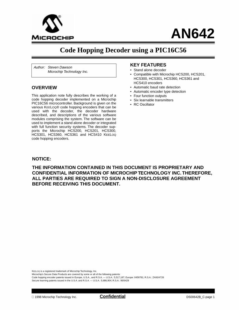
Code Hopping Decoder using a PIC16C56
AN642
S DOC
A
:,187; E 95/542
OVERVIEW
This application note fully describes the working of acode hopping decoder implemented on a MicrochipPIC16C56 microcontroller. Background is given on thevarious KEELOQ® code hopping encoders that can beused with the decoder, the decoder hardwaredescribed, and descriptions of the various softwaremodules comprising the system. The software can beused to implement a stand alone decoder or integratedwith full function security systems. The decoder sup-ports the Microchip HCS200, HCS201, HCS300,HCS301, HCS360, HCS361 and HCS410 KEELOQcode hopping encoders.
Author: Steven Dawson Microchip Technology Inc.
NOTICE:
THE INFORMATION CONTAINED IN THICONFIDENTIAL INFORMATION OF MICRALL PARTIES ARE REQUIRED TO SIGNBEFORE RECEIVING THIS DOCUMENT.
KEELOQ is a registered trademark of Microchip Technology, Inc.Microchip’s Secure Data Products are covered by some or all of the following patentsCode hopping encoder patents issued in Europe, U.S.A., and R.S.A. — U.S.A.: 5,517Secure learning patents issued in the U.S.A. and R.S.A. — U.S.A.: 5,686,904; R.S.A.:
1998 Microchip Technology Inc. Confidential
KEY FEATURES• Stand alone decoder • Compatible with Microchip HCS200, HCS201,
HCS300, HCS301, HCS360, HCS361 and HCS410 encoders
• Automatic baud rate detection• Automatic encoder type detection• Four function outputs• Six learnable transmitters• RC Oscillator
OCUMENT IS PROPRIETARY AND HIP TECHNOLOGY INC. THEREFORE,
NON-DISCLOSURE AGREEMENT
urope: 0459781; R.S.A.: ZA93/47269
DS00642B_C-page 1

AN642
INTRODUCTION TO KEELOQ ENCODERSAll KEELOQ encoders use the KEELOQ code hoppingtechnology to make each transmission by an encoderunique. The encoder transmissions have two parts. Thefirst part changes each time the encoder is activatedand is called the hopping code part. The second part isthe serial number of the encoder, identifying it to adecoder.
Hopping Code
The Hopping Code contains function information, a dis-crimination value, and a synchronization counter. Thisinformation is encrypted by an encryption algorithmbefore being transmitted. A 64-bit encryption key isused by the encryption algorithm. If one bit in the datathat is encrypted changes, the result is that an averageof half the bits in the output will change. As a result, thehopping code changes dramatically for each transmis-sion and can not be predicted.
Function Information
The encoder transmits up to four bits of function infor-mation. Up to 15 different functions are available (0000is related to the reset condition in all the current encod-ers, and can never be transmitted).
Discrimination Value
Stored in the encoder EEPROM, this information isused to check integrity of decryption operation in thedecoder. If known information is inserted into the trans-mitted string before encryption, the same informationcan be used at the decoder to check whether the infor-mation has been decrypted correctly. In the MicrochipHCS encoders, up to 12 bits (including overflow bits)are available.
FIGURE 1: BLOCK DIAGRAM
DS00642B_C-page 2 Confidential
Synchronization Counters
The transmitted word contains a 16-bit synchronizationcounter. The synchronization information is used at thedecoder to determine whether a transmission is valid,or a repetition of a previous transmission. Previouscodes are rejected to safeguard against code grabbers.The HCS300/301 encoder transmits two overflow bitswhich may be used to extend the range of the synchro-nization counter from 65,536 to 196,608 button opera-tions.
Fixed Code
Serial Number
The encoder’s serial number is transmitted every timethe button is pressed. The serial number is transmittedunencrypted as part of the transmission, and serves toidentify the encoder to the decoder. The number can beused during learning operations to calculate the key tobe used for decrypting the transmissions.
Other Status and Function Information
The HCS300/301 encoders include provision for fourbits of function information and two status bits in thefixed code portion of its transmission. The two statusbits indicate whether a repeated transmission is beingsent, and whether the battery voltage is low. TheHCS200/201 does not send repeated transmissioninformation and the bit is permanently set to ‘0’.
Transmission Format
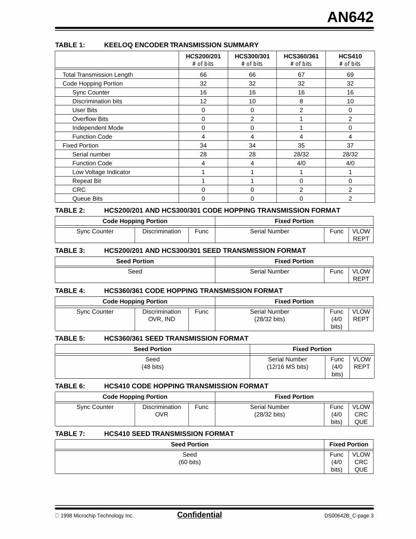
Table 1 contains a summary of the informationcontained in transmissions from each of the KEELOQencoders that can be learned by the Microchipdecoder.
RFReceiver RFIN
S0S1S2S3
PIC
16C
56
EEPROMCSCLKDIO
Learn
Learn
Indication
Init
1998 Microchip Technology Inc.
AN642
TABLE 1: KEELOQ ENCODER TRANSMISSION SUMMARY
TABLE 2: HCS200/201 AND HCS300/301 CODE HOPPING TRANSMISSION FORMAT
TABLE 3: HCS200/201 AND HCS300/301 SEED TRANSMISSION FORMAT
TABLE 4: HCS360/361 CODE HOPPING TRANSMISSION FORMAT
TABLE 5: HCS360/361 SEED TRANSMISSION FORMAT
TABLE 6: HCS410 CODE HOPPING TRANSMISSION FORMAT
TABLE 7: HCS410 SEED TRANSMISSION FORMAT
HCS200/201# of bits
HCS300/301# of bits
HCS360/361# of bits
HCS410# of bits
Total Transmission Length 66 66 67 69Code Hopping Portion 32 32 32 32
Sync Counter 16 16 16 16Discrimination bits 12 10 8 10User Bits 0 0 2 0Overflow Bits 0 2 1 2Independent Mode 0 0 1 0Function Code 4 4 4 4
Fixed Portion 34 34 35 37Serial number 28 28 28/32 28/32Function Code 4 4 4/0 4/0Low Voltage Indicator 1 1 1 1Repeat Bit 1 1 0 0CRC 0 0 2 2Queue Bits 0 0 0 2
Code Hopping Portion Fixed Portion
Sync Counter Discrimination Func Serial Number Func VLOW REPT
Seed Portion Fixed Portion
Seed Serial Number Func VLOW REPT
Code Hopping Portion Fixed Portion
Sync Counter DiscriminationOVR, IND
Func Serial Number(28/32 bits)
Func(4/0 bits)
VLOW REPT
Seed Portion Fixed Portion
Seed(48 bits)
Serial Number(12/16 MS bits)
Func(4/0 bits)
VLOW REPT
Code Hopping Portion Fixed Portion
Sync Counter DiscriminationOVR
Func Serial Number(28/32 bits)
Func(4/0 bits)
VLOW CRCQUE
Seed Portion Fixed Portion
Seed(60 bits)
Func(4/0 bits)
VLOW CRCQUE
1998 Microchip Technology Inc. Confidential DS00642B_C-page 3

AN642
PWM Format
In general, all KEELOQ encoders share a commontransmission format.
• A preamble to improve biasing of decision thresh-olds in superregenerative receivers. The preamble consists of alternate on and off periods, each last-ing as long as a single elemental period.
• A calibration header, consisting of a low period of 10 elemental periods. Calibration actions should be performed on the low period of the header to ensure correct operation with header chopping.
• A string of pulse width modulated bits, each con-sisting of three elements. The first element is high, the second contains the data transmitted and is either high or low, the third element is always low.
• A guard period is usually left between the trans-missions. During this period nothing is transmitted by the encoder.
DS00642B_C-page 4 Confidential
Figure 2 shows the sampling points when samplingdata. The first and last elements are used exclusively toverify the integrity of the received signal. The first ele-ment (sample point A) is always high, the second (sam-ple point B) is the complement of the data bit beingsent, and the final element (sample point C) is alwayslow. Because the period between the low portion of abit (sample point C) and the rising edge of the followingbit (sample point X) can vary somewhat, the rising edgeof the first element (sample point X) is used to resyn-chronize the receiving routine to each incoming bit.
If random noise is being received, the probability of aset of three samples producing a valid combination isonly 2-2 = 1/4. For a string of 66 bits, the correspondingfigure is 2-134. For longer strings, the probability is con-siderably less.
Integrity checking on incoming signals is important.Code hopping signals require significant processing,as well as EEPROM access, to decrypt. Unnecessaryprocessing can be avoided by not attempting to decryptincoming codes that have bit errors.
FIGURE 2: KEELOQ PWM TRANSMISSION FORMATBit Format I Sampling Points
0
1X A B C
2te
2tete
te
1998 Microchip Technology Inc.
AN642
IMPLEMENTATION
The Microchip decoder’s primary hardware compo-nents are a PIC16C56 RISC microcontroller and a93LC46B EEPROM. However, this solution can beimplemented in any PIC16/17 microcontroller with atleast 1K words of programming. The operating fre-quency of the controller is 4 MHz. The microcontrolleris used to capture transmissions from the variousencoders, decrypt transmissions captured, and checkthe validity of the transmission based on the informa-tion in the decrypted transmission and informationstored in the EEPROM. If a transmission from a validencoder is received, the Microchip decoder activatesthe outputs dictated by the transmission.
Encoder information, such as serial number, synchro-nization information, and decryption key are storedexternally in an EEPROM. The EEPROM used is aMicrochip 93LC46B CMOS serial EEPROM. The infor-mation stored in the EEPROM is encrypted to protectthe decoders from cloning. The EEPROM encryption isless secure than the KEELOQ code hopping algorithm.
A more secure implementation of the decoder would beto modify the software in the application note and usea PIC16CXX with an internal EEPROM such as aPIC16C84. In this way communication between thePIC16C56 and EEPROM cannot be monitored.
As can be seen from the section on encoder transmis-sions there are differences in the transmission formatsof the different encoders that are compatible with thesystem. The following section summarizes how the dif-ferences in transmitted data are dealt with by thedecoder.
As the serial number information follows after the codehopping portion of the transmission, any number ofserial number bits can be received and processed. Inthe Microchip decoder being described, 28 bits of theserial number are stored.
The serial number is used to identify the memory blockused to store the 64-bit decryption key for a particularencoder because of the relationship between serialnumber and decryption key. In other words, the serial
1998 Microchip Technology Inc.
number is stored with the key. When a transmission isreceived, the decoder finds the correct memory blockby checking all blocks until a matching serial number isfound. The key is then retrieved from that particularmemory block. A serial number of 000000016 is consid-ered invalid.
Validation of a received transmission consists of twoparts. The first includes checking the integrity of thedecryption operation. Here the decoder compares the12-bit discrimination value received with the stored dis-crimination value. The discrimination value stored forthe HCS300/301 includes the overflow bits.
The second portion of validation involves checkingsynchronization information for that particularencoder. The synchronization counter transmitted byall encoders is 16 bits long. Two copies of the full syn-chronization counter are stored for all valid encoders.The storing of two copies of the synchronization infor-mation protects the decoder from loosing synchroniza-tion with an encoder if one of the counters is corrupted.
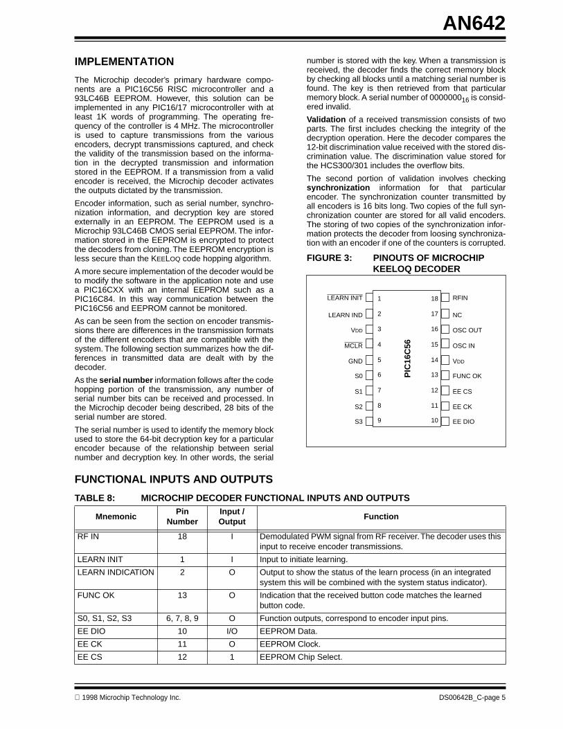
FIGURE 3: PINOUTS OF MICROCHIP KEELOQ DECODER
18
17
16
15
14
13
12
11
10
LEARN INIT
LEARN IND
VDD
MCLR
1
2
3
4
GND
S0
S1
RFIN
NC
OSC OUT
OSC IN
VDD
FUNC OK
EE CS
S2 EE CK
S3
5
6
7
8
9 EE DIO
PIC
16C
56
FUNCTIONAL INPUTS AND OUTPUTS
TABLE 8: MICROCHIP DECODER FUNCTIONAL INPUTS AND OUTPUTS
MnemonicPin
NumberInput / Output
Function
RF IN 18 I Demodulated PWM signal from RF receiver. The decoder uses this input to receive encoder transmissions.
LEARN INIT 1 I Input to initiate learning.
LEARN INDICATION 2 O Output to show the status of the learn process (in an integrated system this will be combined with the system status indicator).
FUNC OK 13 O Indication that the received button code matches the learned button code.
S0, S1, S2, S3 6, 7, 8, 9 O Function outputs, correspond to encoder input pins.
EE DIO 10 I/O EEPROM Data.
EE CK 11 O EEPROM Clock.
EE CS 12 1 EEPROM Chip Select.
DS00642B_C-page 5

AN642
PROGRAM FLOW
The software for the Microchip decoder has been writ-ten for the PIC16C56 microcontroller. The compilerused is MPASM. The operating frequency of thePIC16C56 is 4 MHz. The clock speed is important asthe reception routine (RECEIVE) has some critical tim-ing specifications. Other decoder functions that rely ona 4 MHz clock speed are the hold times of the variousoutputs, time-outs, etc.
The main program flow is described here. Moredetailed descriptions of the modules can be found fur-ther in the application note. On power-up the decoderreads the learn indicator from the external EEPROM.The status flags are checked to see if a learn routinewas interrupted when the microcontroller was reset. If
DS00642B_C-page 6 Confidential
so, it is assumed the learn cycle was not successfullycompleted and the encoder at the learn indicator sub-sequently deleted (WIPE_TX).
The encoder then enters the main loop where it spendsmost of its time. The main loop checks to see if thelearn button is being activated (TST_LEARN). If so, thedecoder enters the learn mode.
If learn has not been initiated, the microcontroller thenchecks for transmissions from encoders (RECEIVE). If64 bits (HCS encoders) are received, the microcontrol-ler validates the transmission received. If the transmis-sion received is a valid transmission from an encoderlearned into the system, the system sets the appropri-ate outputs (M_BUT).
FIGURE 4: MICROCHIP DECODER MAIN PROGRAM FLOW
Reset
Get LearnIndicator
Reset Due ToFailed Learn?
Delete TXAt LearnPosition
WIPE_TX
MAIN
Yes
NoLoop BackPoint
MAIN2
LearnPressed?
M_LOOP2->TST_LEARN Yes
Learn Routine
No
Check ForEncoder TXRECEIVE
Received 56Or 66 Bits?M_LOOP2No
TransmissionValidation
Yes
1998 Microchip Technology Inc.

AN642
FUNCTIONAL MODULES
Reception
The reception routine (called RECEIVE) is based on areliable algorithm which has successfully been used inprevious implementations of KEELOQ decoders. Auto-matic baud rate detection is used to compensate forvariations in baud rate of different encoders of a specifictype, as well as the difference in baud rate between dif-ferent encoders (HCS200, and HCS300). The receptionroutine is able to handle 64-bit transmissions. This iseasily extented to receive more bits. The reception rou-tine is able to determine the type of encoder by the num-ber of bits in the transmission.
The reception algorithm performs the following func-tions when an output is detected from the receiver:
1. Calibrate on the header low period to determinethe actual elemental period for the transmissionbeing received. The required elemental period is10% of the low header period. In the diagrambelow (Figure 5) the header calibration samplepoints are marked 1 through 3. The calibrationflow chart (Figure 6) shows at what points in thesource code samples 1, 2, and 3 are taken. Ele-mental periods outside the capture range of thealgorithm (either too long or too short) should berejected, since they would be due either to noiseor to reception of an incomplete signal.
2. Using the determined elemental period, threesamples after the first rising edge following theheader are taken. The first sample is taken halfan elemental period after the rising edge (sam-ple 4); the second, one elemental period later(sample 5), and the third, another one elementalperiod later (sample 6). The first sample must behigh, the second could be either high or low, andthe third sample must be low. If either the first orthe third sample is not as expected, the attemptat capturing a transmission is abandoned. In thediagram below (Figure 5), the data samplepoints are points 4 through 6. The flow chartdescribing data reception (Figure 7) shows
1998 Microchip Technology Inc.
where in the code the samples are taken.3. If all 64 bits have been captured, each with the
correct first and third elements, the transmissioncan be assumed to be correct, and decryptioncan commence.
The receiving routine should be called often enough toensure that the high portion in the header is not missed(Sample 1, Figure 5).
In systems where the receive routine is called to checkif there is activity on the receiver input, the routineshould poll the input for a valid transmission for at leastthe time taken to complete one transmission if activityis detected on the input line. This makes provision forthe receive routine being called while a transmission isin progress. Having missed the first header, the firsttransmission will be invalid and be discarded. Thedecoder should continue sampling the input throughthe guard time in order to catch the next header andtransmission (i.e., for a decoder designed to captureHCS300 transmissions the time spent polling for a validtransmission should be at least 100 ms if activity isdetected in the input line).
The diagram below (Figure 5) gives all the major sam-pling points in the receive algorithm.
FIGURE 5: SAMPLING POINTS USED IN RECEIVE ALGORITHM
Note: The sample points are labeled in thereceive routine flow diagrams that follow.
1 2 3 4 5 6 7 4 5
Preamble Header Data
DS00642B_C-page 7

AN642
Flow Diagrams
The first flow diagram (Figure 6) describes the calibra-tion routine which is used to determine the actual trans-mission rate of the encoder so that the decoder cancompensate for deviations from nominal timing. Thereare four different exit points, each of which shouldbranch to a point in the program where housekeepingand input monitoring can be resumed. There is onlyone exit point for a valid calibration operation (RCV7).At this point, it is assumed that a valid header has beenreceived and that a string of data bits will follow.
The second flow diagram (Figure 7) handles the recep-tion of bits once the calibration routine has been suc-cessfully completed. The data bits are all sampledthree times each to ensure that a noise free transmis-sion has been received. The receive routine uses thecalibrated elemental period, determined in the calibra-tion routine, to ensure that the samples are spaced cor-rectly. The routine resynchronizes itself on the risingflank of each bit. Provision for identification of theencoder type, based on the number of bits received, isincluded. KEELOQ encoders transmit at least 66 bits.The decoder only receives 64 bits of the transmission,the remaining status bits aren’t used by this decoder.The last two bits of the HCS300 transmission, VLOWand Repeat, are ignored by the Microchip decoder.
If all of the control samples in all of the bits are sampledcorrectly (i.e., the first element is high and the last ele-ment is low), the routine checks whether 56 bits havebeen received correctly. If not, the routine returns to thecalling procedure.
DS00642B_C-page 8 Confidential
FIGURE 6: CALIBRATION FLOW CHART
CalibrateRECEIVE
Input?Low Invalid
HeaderRMT_0
High 1
Reset Time-outCounter
Input?RCV1
High
Yes
Low
Clear CalibrationCounter
RCV2
Update Time-outCounter
RCV5 No
Input?RCV3
Low TooLong?RCV4
YesHigh
CalibrationCounter/10
RCV6
TooShort?RCV6
Yes InvalidHeaderRMT_0
No
LoadCal Counter
RCV7
ReceiveDataDL1
No
Time-out?
2
3
1998 Microchip Technology Inc.

AN642
FIGURE 7: DATA RECEPTION IN RECEIVE
ReceiveDataRCV7
Wait HalfBit Period
DL1
Input?Low
High
Wait FullBit Period
DL2
Input?High
Low
Data = 1 Data = 0
Wait FullBit Period
DL3
Last Bit?No
Yes
High
Low Input?RCV9/RCV10
No
Time-out?
Yes
No Received56 Bits?
RMT0
Yes
CleanupRMT2
ReceptionComplete
RMT1
3
4
5
Input?High
Low 6
7
Invalid
1998 Microchip Technology Inc. Confidential DS00642B_C-page 9
AN642
Validation
Once a complete transmission has been received froman encoder, the transmission needs to be validatedbefore any further action is taken. Validation consists ofthe following steps:
1. Check the serial number (24, 28 bits) against thestored encoder serial numbers (M_SERIAL).
2. Decrypt the transmission received (M_HOP).3. Compare the discrimination value in the
decrypted hopping portion of the transmissionagainst the stored discrimination value (M_DIS).
4. Check if the synchronization counter falls withinthe resynchronization window (M_CHECK1).
5. Check if the synchronization counter falls withinthe open window. If not, then decoderresynchronization is necessary (M_CHECK2).
6. If resynchronization is necessary wait for asecond transmission from the encoder with aconsecutive synchronization counter.
7. Update the synchronization counter inEEPROM (M_UPDATE).
8. Set the appropriate outputs (M_BUT).9. Return to MAIN routine and continue normal
housekeeping chores.
DS00642B_C-page 10 Confidential
Discrimination Values
After decryption, the Code Shift Register (CSR) usedby the KEELOQ decryption algorithm contains the same32 bits of information originally encrypted in theencoder before transmission. 12 of these bits are dis-crimination bits.
The decryption operation can be checked by compar-ing parts of the decrypted 32-bit word (the discrimina-tion values) with known values.
For the HCS300/301 the user can program the discrim-ination bits to contain any value. In the HCS360/361 thediscrimination bits are the least significant 8 bits of theserial number. The discrimination bits are stored in theexternal EEPROM during learn. By comparing the dis-crimination bits to the bits expected, the integrity of thedecryption can be easily verified.
Note: The overflow bits (when available in anencoder) are treated as part of the discrim-ination value. For example, these bits canbe set when the HCS300/301 encoders areprogrammed. When the encoder’s counteroverflows the overflow bits are individuallycleared extending the counter range from65,536 to 196,608. The clearing of the over-flow bits will result in an ‘erroneous’ discrim-ination value being decrypted because theoverflow bits are stored as part of the dis-crimination value. The transmission will betreated as an invalid transmission by thisdecoder and the transmission discarded. Inorder to avoid this, the HCS300/301’s over-flow bits should both be programmed as ‘0’and the synchronization counter started at‘0’.
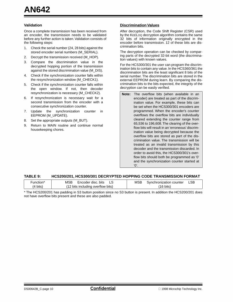
TABLE 9: HCS200/201, HCS300/301 DECRYPTED HOPPING CODE TRANSMISSION FORMAT
* The HCS200/201 has padding in S3 button position since no S3 button is present. In addition the HCS200/201 doesnot have overflow bits present and these are also padded.
Function*(4 bits)
MSB Encoder disc. bits LS (12 bits including overflow bits)
MSB Synchronization counter LSB(16 bits)
1998 Microchip Technology Inc.

AN642
Synchronization Checking
The synchronization information is used at the decoderto determine whether the transmission is valid orwhether it is a repetition of a previous transmission.Repetitious codes are rejected to safeguard the systemagainst code grabbers.
The transmitting encoder has a 16-bit synchronizationcounter, stored in EEPROM, which is incrementedevery time the encoder is activated. The synchroniza-tion counter value is stored in the decoder’s EEPROMevery time a valid transmission is received from a par-ticular encoder. When a following transmission isreceived from the same transmitter it is possible toquickly verify whether the transmission is valid. Forexample, a grabbed code from the legitimate user’sprevious transmission will result in a synchronizationcounter value, that has already been received, beingdecrypted.
Note: Two copies of the synchronization counterare stored. The reason for this is should thepower go down during an EEPROM write,a corrupted counter value would be readwhen the device is later powered up,resulting in encoder transmissions errone-ously being discarded as invalid.
1998 Microchip Technology Inc.
Provision must be made for the transmitter beingpressed while out of range of the decoder. TheMicrochip decoder does this by allowing two ‘synchro-nization windows’. The open window is a reception ofa transmission where the synchronization counter is 1to 16 higher than the previous counter value received.The reception of such a signal will result in an immedi-ate counter update by the decoder and the appropriateoutputs being activated.
If the transmitter is pressed more than 16 times out ofrange of the receiver, resynchronization needs to takeplace. The resynchronization window is a half of thetotal counter range, 32K big. During resynchronizationthe decoder waits for two consecutive transmissionsfrom the encoder before resynchronization takes placeand the resynchronized counters updated in thedecoder’s EEPROM. When the decoder receives atransmission with a synchronization counter valuemore than 16 above the stored counter value and lessthan 32,768 counts above the stored value, thedecoder temporarily stores the value of the synchroni-zation counter received. If the next transmissionreceived has a sequential synchronization countervalue the decoder resynchronizes on the last transmis-sion received and activates the appropriate outputs.
If any of the above tests fail the transmission receivedis discarded. It is easy to change the size of the variouswindows in the source code. Modifications to the syn-chronization windows can be made in the M_CHECKroutine.
FIGURE 8: DECODER WINDOW OPERATION
Open Window
Block 32KWindow
Resync. 32KWindow 16 Values in
Open Window
Entire Windowrotates With Use
DS00642B_C-page 11

AN642
FIGURE 9: VALIDATION FLOW CHART TRANSMISSION VALIDATION FLOWCHART
TransmissionValidation
Step IndicatorChecked All Users?
M_NEXTYes
No
No
Get Serial #From EEPROM
M_SERIAL
Same As
Yes
DecryptTransmission
M_HOP
No
Yes
No
Yes
Yes
No
Yes
Return ToMain
Serial #
DiscriminationValues Equal?
M_DIS
RESYNCSet?
M_CNT
Get CountersFrom EEPROM
M_CNT1
WithinResync Window?
M_CHECK1
WithinOpen Window?
M_CHECK2
Update StoredCounters
M_UPDATE
Set AppropriateOutputsM_BUT
Get StoredCounters
No
Yes
CountersSequential?M_CHECK0
Store CountersIn RAM
M_RESYNC
Received?
No
DS00642B_C-page 12 Confidential 1998 Microchip Technology Inc.
AN642
Function Interpretation
In a single-chip system, where the code hoppingdecoder and the control program are combined intoone device, the function code is interpreted to deter-mine what the system must do. One function can beused to arm the system and lock the vehicle, a secondto disarm the system and unlock the vehicle, and a thirdto open the trunk.
The four function bits in the encrypted portion of atransmission can be used to determine the button(s)pressed on the transmitter. Up to 15 functions can beimplemented in this way, 0000 being related to a resetstate.
The four function bits transmitted by the KEELOQencoders are labeled F2, F1, F0 and F3. Thesecorrespond to S2, S1, S0, and S3 in the HCS300/301,S2, S1, S0, and S2 in the HCS200/201. The Sn bits inturn correspond with the values of the control inputs ofthe encoders.
In the Microchip decoder the function code receivedfrom the encoder is put onto the function outputs (S0 toS3) if a valid transmission is received (M_BUT). In addi-tion, if the button code that was learned into the systemis received, the FUNC OK output is activated.
Output Activation
The Microchip decoder has five momentary outputsnamely S0, S1, S2, S3, and FUNC OK. As described inthe section on Function Interpretation these outputsare a function of the inputs activated on the encoder.The momentary outputs are activated for 524 ms andextended for 524 ms if a repeated transmission isreceived. If a new valid transmission with a differentfunction code is received during output activation, theoutputs are switched off for 131 ms and the newfunction output activated.
FUNC OK is set if the function code received by thedecoder is the same as the function code receivedduring the learn cycle. The routine displaying thefunction code information and checking whether thefunction code received is the same as the one usedduring learn is called M_BUT.
1998 Microchip Technology Inc. Confidential
Key Generation
Before transmitting the hopping portion of the code anencoder uses a 64-bit read protected encryption key toencrypt the information. In order to read the informationcontained in the hopping portion of the code it isnecessary for the decoder to decrypt the data.
The use of a manufacturer’s code in key generationallows a unique relationship between encoder serialnumber and encryption/decryption key pair. Thisenables each manufacturer to produce encoders thatcannot be cloned by competitors. Security of themanufacturer’s code is critical to product security andas a result the manufacturer’s code (MKEY) is stored inROM in the PIC16C56 microcontroller.
Two key generation techniques are used in the KEELOQdecoders. The first is a normal key generationalgorithm which is used in the Microchip decoderdescribed. The second key generation technique usesa feature on the Microchip HCS encoders called SEEDtransmission. In this mode the transmitter transmits aSEED programmed during learn instead of the codehopping.
Normal Key Generation
The Microchip decoder described uses the normal keygeneration technique to generate decryption keys forthe encoders. Normal key generation is performed intwo steps as shown in the flow chart in Figure 10. Thefirst step generates the least significant 32 bits of thedecryption key, the second the most significant 32 bitsof the decryption key. The relationship between decryp-tion key and serial number during key generation isachieved by using the serial number of the encoder asa seed for the decryption routine. The length of theserial number is 28 bits for the HCS200/201 and theHCS300/301. The serial number of the encoder ispadded to make the key generation seed 32 bits. Toallow the most significant 32 bits of the decryption keyto differ from the least significant 32 bits the serial num-ber is padded to 32 bits differently on each step. Themanufacturer’s code is used as the key for the decryp-tion operation during key operation. Table 10 shows thedifferent padding techniques used.
TABLE 10: SEED GENERATION PADDING FOR VARIOUS ENCODERS
HCS encoders
Seed1 padding 2*******16
Seed2 padding 6*******16
DS00642B_C-page 13
AN642
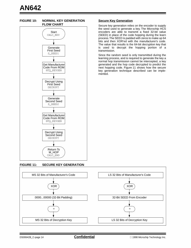
FIGURE 10: NORMAL KEY GENERATION FLOW CHART
StartCALC_KEY
GenerateFirst SeedS_SEED1
Decrypt UsingFirst SeedDECRYPT
Get ManufacturerCode From ROM
NTQ_KEYGEN
GenerateSecond Seed
S_SEED2
Decrypt UsingSecond Seed
DECRYPT
Get ManufacturerCode From ROM
NTQ_KEYGEN
Return ToM_HOP
CALC_END
FIGURE 11: SECURE KEY GENERATION
DS00642B_C-page 14 Confidential
Secure Key Generation
Secure key generation relies on the encoder to supplythe seed used to generate a key. The Microchip HCSencoders are able to transmit a fixed 32-bit value(SEED) in place of the code hopping during the learnprocess. The SEED is padded with zeros to make up 64bits and then XOR’ed with the manufacturer’s code.The value that results is the 64-bit decryption key thatis used to decrypt the hopping portion of atransmission.
Since the random seed is only transmitted during thelearning process, and is required to generate the key anormal hop transmission cannot be intercepted, a keygenerated and the hop code decrypted to predict thenext hopping code. Figure 11 shows how the securekey generation technique described can be imple-mented.
MS 32 Bits of Manufacturer’s Code
XOR
0000...00000 (32-Bit Padding)
=
MS 32 Bits of Decryption Key
LS 32 Bits of Manufacturer’s Code
XOR
32-Bit SEED From Encoder
=
LS 32 Bits of Decryption Key
1998 Microchip Technology Inc.

AN642
Decryption
After receiving a valid transmission the decoderdecrypts the code hopping portion of the transmittedcode. This is done with the help of the KEELOQ decryp-tion algorithm. Each encoder has its own encryptionkey which is related to the serial number of the encoderand is calculated when the encoder is programmed. Inorder to decrypt the transmission a decryption key iscalculated by the decoder during the learn cycle andstored in the EEPROM. The decryption routine is calledDECRYPT.
The KEELOQ decryption algorithm is used to decryptthe 32-bit code hopping portion of KEELOQ transmis-sions. A 32-bit Code Shift Register (CSR) contains thereceived code, and a 64-bit register contains thedecryption key
The 64-bit decryption key is retrieved from EEPROMinto RAM for every decryption operation. Several 64-bitkeys are stored in memory, one for each validtransmitter. The key particular to a given encoder isretrieved to decrypt the code hopping portion of aparticular encoder. The key to be retrieved is identifiedby the serial number of the encoder that is transmitted.
FIGURE 12: THE KEELOQ DECRYPTION ALG
1998 Microchip Technology Inc.
The block diagram (Figure 12) explains the operationduring each iteration of the decryption algorithm. Anon-linear function (NLF) is used to produce a single bitfrom five bits in the CSR. This output is combined, viaan exclusive-OR function, with two CSR bits and a sin-gle-bit from the key register to form an output. At theend of each cycle, the key register is rotated left, andthe CSR is rotated left. The MSB (bit 3,7) of the CSR isdiscarded, and the output from the exclusive-ORfunction is inserted into the LSB (bit 0,0) of the CSR.
The decryption operation requires 528 iterations. Inother words, the operation in the block diagram shouldbe executed 528 times before the decrypted data willappear in the CSR.
The non-linear function (NLF, Table 11) is intended toobscure any linear relationships that might otherwiseexist in the encrypted output. The NLF is listed in theform of a 5-bit lookup table, in which the five input bitsare I4 = CSR3,6, I3 = CSR3,1, I2 = CSR2,3, I1 = CSR1,0,and I0 = CSR0,0.
ITHM
ORTABLE 11: NON-LINEAR FUNCTION OUTPUTI4 I3 I2 I1 I0 NLF I4 I3 I2 I1 I0 NLF
0 0 0 0 0 0 1 0 0 0 0 00 0 0 0 1 1 1 0 0 0 1 00 0 0 1 0 1 1 0 0 1 0 10 0 0 1 1 1 1 0 0 1 1 10 0 1 0 0 0 1 0 1 0 0 10 0 1 0 1 1 1 0 1 0 1 00 0 1 1 0 0 1 0 1 1 0 10 0 1 1 1 0 1 0 1 1 1 00 1 0 0 0 0 1 1 0 0 0 00 1 0 0 1 0 1 1 0 0 1 10 1 0 1 0 1 1 1 0 1 0 00 1 0 1 1 0 1 1 0 1 1 10 1 1 0 0 1 1 1 1 0 0 10 1 1 0 1 1 1 1 1 0 1 10 1 1 1 0 1 1 1 1 1 0 00 1 1 1 1 0 1 1 1 1 1 0
NLF
1,7MSB Code Shift Register LSB
3,73
3,6 3,1 2,3 1,0 0,0
1,7
MSB Key Register LSB
2 01
7 6 45 3 2 01
XOR
DS00642B_C-page 15

AN642
Learn
A learn indicator is used by the Microchip decoder tokeep track of the next position a learn is to take place.The encoder positions in EEPROM form a rotatingbuffer where the next transmitter to be written over isthe transmitter at the tail of the buffer. The LEARN INITinput is active low and the LEARN IND output activehigh. Learn is initiated by momentarily pressing the
DS00642B_C-page 16 Confidential
LEARN button. The decoder uses the current learnposition as a scratch pad area. This means that anunsuccessful learn deletes the information stored atthat learn position. The learn indicator is not incre-mented if the learn was unsuccessful. The followingflow diagram shows the learning operation.
FIGURE 13: LEARN OPERATION
LEARN MODE
No
Press Learn But
But StillYes
Pressed?
Learn NewTransmitter
LED On Solid
First CodeReceived?
No
LED Off
Second CodeReceived?
No
Yes
CodeValidated?
Yes
No
Exit LearnTurn LED Off
END
No
Time GreaterYes
Than 33.6 Sec.
No
Time GreaterYes
Than 33.6 Sec.
LED On SolidFor 1 Second
Erase Memory
NoTime Greater
Yes
Than 8.4 Sec.
Yes
Blink LED
1998 Microchip Technology Inc.

AN642
Learn (cont’d)
The following checks are performed on the receivedcodes to determine if the transmitter is valid:
1. The first code that is received is checked for bitintegrity (RECEIVE).
2. The stored serial numbers are then searched tocheck if a transmitter being is re-learned. If are-learn is taking place that position is used orelse the position pointed to by the learn indicatoris used (M_SERIAL).
3. The serial number is stored in EEPROM andused to generate a decryption key(CALC_KEY).
4. The hop code is decrypted (M_HOP) and theresult stored temporarily (M_SL_UPDATE). Thecounter and serial number are stored(M_UPDATE).
5. The serial number of the second code that isreceived is compared to the first received serialnumber (M_SERIAL).
6. The second hop code is decrypted (M_HOP)and the discrimination values compared(M_DIS).
7. The synchronization counters of the decryptedcodes are compared to check that they aresequential codes (M_UPDATE).
8. If all the checks pass the learn was successfuland the learn indicator is incremented else theposition is erased.
Operation of Learn
1. Press and release the LEARN button. IndicatorLED will turn on to indicate learn mode.
2. Press transmitter button. The LED will turn off.3. Press transmitter a second time. The LED will
blink to indicate that the transmitter was learnedsuccessfully.
4. Repeat steps 1-3 to learn up to six transmitters.The seventh transmitter will overwrite the firsttransmitter that was learned.
5. Learn will be terminated if two non-sequentialcodes were received or if two acceptable codeswere not decrypted within 33.6 seconds. Aninvalid learn will be indicated by the LED turningon solid for one second.
6. Erasing all the transmitters is accomplished bypressing and holding the LEARN button for 8.4seconds. The LED will turn off at the end of the8.4 seconds to indicate that all the transmitterswere erased. The learn indicator is reset to thefirst position.
1998 Microchip Technology Inc. Confidential
TIMER0 (RTCC) Multiplexing
A time keeping scheme is needed to ensure that thesystem timing is not abandoned while receiving anincoming signal, during learn cycles, key generationand decryption. The system timing is used to allow peri-odic monitoring of sensors and pulsing outputs with aspecific period.
TIMER0 is used to keep track of system time. TIMER0is an 8-bit timer on the PIC16C56. On the Microchipdecoder described, TIMER0 is prescaled to incrementevery 256 instruction cycles. This makes TIMER0 veryuseful for keeping track of real time. While variousroutines are being run, including receive routines anddecryption, TIMER0 is periodically checked for atime-out value calculated at the beginning of a certainperiod (i.e., switch off time of a LED).
The routine checking TIMER0 is called TST_RTCC.The most significant bit (MSB) of TIMER0 changesevery 32 ms. In order to extend the range of TIMER0 2additional 8-bit counters are used, CNT_LW andCNT_HI, which extends the range TIMER0 to 134 sec-onds. The MSB of TIMER0 is mirrored in the MSB ofthe STATUS register during startup. During TST_RTCCthe 2 bits are compared. If the bits differ, the MSB ofTIMER0 has changed indicating that 32 ms haspassed. The MSB of STATUS is changed to match theMSB of TIMER0 and the extended counter(CNT_LWand CNT_HI) incremented.
The second portion of the TST_RTCC routine checksappropriate time-out values based on the systemstatus bits in SREG (i.e. To check for the 30s time-outin the learn routine TST_RTCC checks to see if bitthree of CNT_HI is set).
DS00642B_C-page 17

AN642
ROM MEMORY MAP(8-BIT BYTES)
TABLE 12: ROM MEMORY MAP (8-BIT BYTES)
Word Address
Mnemonic Description
40 MKEY_064-bit41 MKEY_1
42 MKEY_243 MKEY_3
Manufacturer’s Code(Used to generatedecryption keys)
44 MKEY_445 MKEY_546 MKEY_647 MKEY_748 Unused49 Unused4A EKEY_0 64-bit
EEPROM Key4B EKEY_14C EKEY_24D EKEY_34E EKEY_4
(Used to encrypt EEPROM data)
4F EKEY_550 EKEY_651 EKEY_7
DS00642B_C-page 18 Confidential
EEPROM MEMORY MAP(16-BIT WORDS)
TABLE 13: EEPROM MEMORY MAP(16-BIT WORDS)
Address Mnemonic Address Mnemonic
00 USER0 20 CNT20
01 Learn Ind. 21 CNT21
02 DIS0 22 SER20
03 DIS1 23 SER21
04 USER2 24 KEY20
05 USER3 25 KEY21
06 USER4 26 KEY22
07 USER5 27 KEY23
08 DIS2 28 CNT30
09 DIS3 29 CNT31
0A DIS4 2A SER30
0B DIS5 2B SER31
0C USER6 2C KEY30
0D USER7 2D KEY31
0E USER8 2E KEY32
0F USER9 2F KEY33
10 CNT00 30 CNT40
11 CNT01 31 CNT41
12 SER00 32 SER40
13 SER01 33 SER41
14 KEY00 34 KEY40
15 KEY01 35 KEY41
16 KEY02 36 KEY42
17 KEY03 37 KEY43
18 CNT10 38 CNT50
19 CNT11 39 CNT51
1A SER10 3A SER50
1B SER11 3B SER51
1C KEY10 3C KEY50
1D KEY11 3D KEY51
1E KEY12 3E KEY52
1F KEY13 3F KEY53
USER These words are reserved for user storage.
SER The encoder serial number storage
KEY These words contain the decryption key for each encoder.
DIS Discrimination values and function code storage.
CNT Two copies of the synchronization counter are stored for each encoder to prevent loss of synchronization information due to EEPROM write failure.
1998 Microchip Technology Inc.

AN642
RAM MEMORY MAP (8 BIT BYTES)
TABLE 14: RAM MEMORY MAP (8 BIT BYTES)
Address Mnemonic Description
07 FLAGS Decoder flags
08 ADDRESS Address register - points to address in EEPROM
09 TXNUM Current transmitter
0A OUTBYT General data register, mask register used in decryption
0B CNT0
Loop counters0C CNT1
OD CNT2
OE CNT_HI16-bit clock counter
OF CNT_LO
10 TMP1
Temporary registers11 TMP2
12 TMP3
13 TMP4
14 CSR4
64-bit shift registerUsed in reception, decryption and key generation
15 CSR5
16 CSR6
17 CSR7
18 CSR0
19 CSR1
1A CSR2
1B CSR3
1C OLD_BUT Store previous button code
1D RAM_HI16-bit RAM counter (used in resynchronization)
1E RAM_LW
1F SREG Program state register
1998 Microchip Technology Inc. Confidential DS00642B_C-page 19

AN642
ALTERNATE NAMES AND FUNCTIONS
Many of the memory locations in RAM are used by multiple routines. A list of alternate names and functions are givenin the table below.
TABLE 15: ALTERNATE NAMES AND FUNCTIONS
Address Mnemonic Also known as Description
11 KEY0 TMP2
64-bit shift register holds decryption key
10 KEY1 TMP1
12 KEY2 TMP3
13 KEY3 TMP4
14 KEY4 CSR4
15 KEY5 CSR5
16 KEY6 CSR6
17 KEY7 CSR7
18 HOP1 CSR0
32-bit hop code register19 HOP2 CSR1
1A HOP3 CSR2
1B HOP4 CSR3
1B DAT1 CSR3
32-bit data register1A DAT2 CSR2
19 DAT3 CSR1
18 DAT4 CSR0
OD ETMP1 CNT2
Extended 32-bit buffer used during key generationas a 32-bit buffer
1C ETMP2 OLD_BUT
1D ETMP3 RAM_HI
1E ETMP4 RAM_LW
17 SER_0 CSR7
24/28-bit serial number, stores received transmissionopen 32-bits
16 SER_1 CSR6
15 SER_2 CSR5
14 SER_3 CSR4
1B FUNC CSR3 Button code and user nibble of discrimination value
1A DISC CSR2 Discrimination value
19 CNTR_HI CSR116-bit received counter
18 CNTR_LW CSR0
DS00642B_C-page 20 Confidential 1998 Microchip Technology Inc.

AN642
DEVICE PINOUTS
The device used in the application note is a PIC16C56 PDIP.
TABLE 16: DEVICE PINOUTS
TIMING PARAMETERS
TABLE 17: TIMING PARAMETERS
PINPIC16C56 function
Decoder function PINPIC16C56 function
Decoder function
1 PORTA Bit2 LEARN Input Active Low 18 PORTA Bit1 RF Input2 PORTA Bit3 LRN IND Output Active
High17 PORTA Bit0 Not used
3 TIME Connect to VDD 16 Osc In RC osc (4 MHz)4 /MCLR Brown out detect 15 Osc Out5 GND Ground 14 VDD +5V supply6 PORTB Bit0 S0 13 PORTB Bit7 FUNC OK7 PORTB Bit1 S1 12 PORTB Bit6 EEPROM CS (1)8 PORTB Bit2 S2 11 PORTB Bit5 EEPROM CLK (2)9 PORTB Bit3 S3 10 PORTB Bit4 EEPROM DIO (3+4)
Parameter Typical Unit
Output activation duration 524 ms
Output pause if new function code received 131 msErase all duration 8.4 sLearn mode time-out 33.6 sLearn successful LED flash duration 4.2 sLearn successful LED flash rate 3.8 HzLearn failure LED on duration 1 s
1998 Microchip Technology Inc. Confidential DS00642B_C-page 21

AN642
SOURCE CODE LISTING
A diskette is supplied containing source code for theMicrochip decoder in the file mcdec12.asm. The codehas been compiled using MPASM v01.30.01. Certainfunctions are dependent on the oscillator speed for cor-rect functioning. Examples of time dependent functionsinclude RECEIVE and TST_RTCC. The PIC16C56Microcontroller should run at 4 MHz.
LIST OF IMPORTANT FUNCTIONS
DS00642B_C-page 22 Confidential
Function Name Description Function length
CALC_KEY Key generation routine. 62
DECRYPT Decryption routine for Code Hop. 61EEREAD The data in the EEPROM at ADDRESS is read and decrypted to TMP1
and TMP2. Note that TMP1, TMP2 and ADDRESS are user defined reg-isters.
31
EEWRITE The data in TMP1 and TMP2 is encrypted and written to the EEPROM at ADDRESS. Note that TMP1, TMP2 and ADDRESS are user defined reg-isters.
48
M_DIS Check discrimination value. 19M_CNT Check synchronization (counter) values. 69RECEIVE Start of the RF receive routine. 121TST_LEARN1 Check for learn mode and entry to learn. 21TST_RTCC Check TIMER0 and do whatever real time tasks are required. 38
1998 Microchip Technology Inc.
AN642
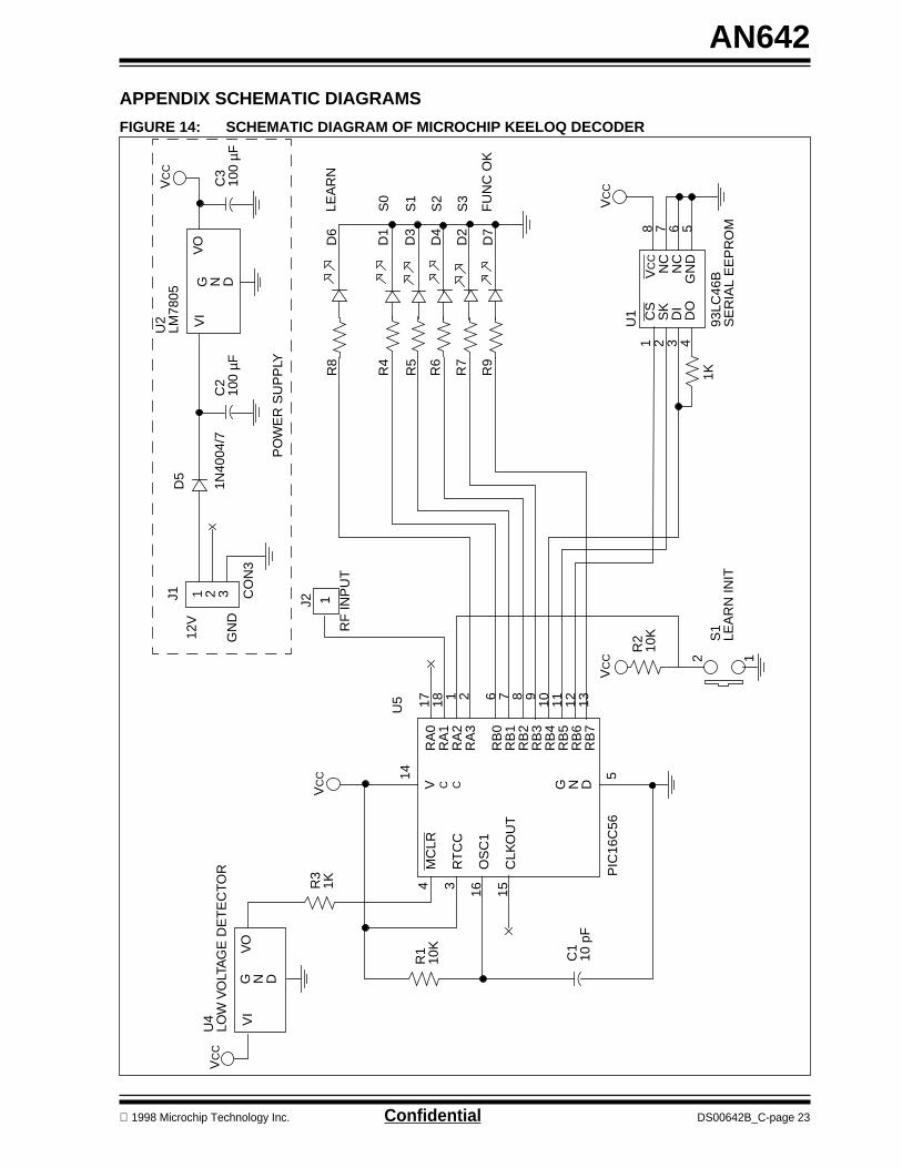
APPENDIX SCHEMATIC DIAGRAMS
FIGURE 14: SCHEMATIC DIAGRAM OF MICROCHIP KEELOQ DECODER
17 18 1 2 6 7 8 9 10 11 12 13
RA
0R
A1
RA
2R
A3
RB
0R
B1
RB
2R
B3
RB
4R
B5
RB
6R
B7
MC
LR
RT
CC
OS
C1
CLK
OU
T
D6
D1
S1
S2
S3
FU
NC
OK
LEA
RN
D3
D4
D2
D7
R8
R4
R5
R6
R7
R9
S0
V C C G N D
G N D
VC
CU
4LO
W V
OLT
AG
E D
ET
EC
TOR
VI
VO
R3
1KV
CC
R1
10K
C1
10 p
F
PIC
16C
56
14U
5
5V
CC
R2
10K
2 1
S1
LEA
RN
INIT
4 3 16 15
1J2
RF
INP
UT
CS
SK
DI
DO
VC
CN
CN
CG
ND
93LC
46B
VC
C
U1
1 2 3 4
8 7 6 5
SE
RIA
L E
EP
RO
M
1 2 3
12V
GN
D
D5
CO
N3
J1
1N40
04/7
C2
100
µF
PO
WE
R S
UP
PLY
G N D
U2
LM78
05
VI
VO
VC
C
C3
100
µF
1K
1998 Microchip Technology Inc. Confidential DS00642B_C-page 23

AN642
FIGURE 15: TYPICAL GARAGE DOOR OPENER SCHEMATIC
17 18 1 2 6 7 8 9 10 11 12 13
RA
0R
A1
RA
2R
A3
RB
0R
B1
RB
2R
B3
RB
4R
B5
RB
6
MC
LR
RT
CC
OS
C1
CLK
OU
T
D10
RE
LAY
SP
ST
S1
S0
LEA
RN
J2 CO
N1
D8
1N40
04/7
Q1
S0
V C C G N D
G N D
VC
CU
4LO
W V
OLT
AG
E D
ET
EC
TOR
VI
VO
R3
1K
VC
C
R1
10K
C1
10 p
F
PIC
16C
56
14U
5
5V
CC R
210
K
2 1
S1
LEA
RN
INIT
4 3 16
J3
RF
RE
CE
IVE
R M
OD
ULE
CS
SK
DI
DO
VC
CN
CN
CG
ND
93LC
46B
VC
C
U1
8 7 6 5
SE
RIA
L E
EP
RO
M
1 2 3
12V
GN
D
D5
CO
N3
J1
1N40
04/7
C2
100
µF
PO
WE
R S
UP
PLY
G N D
U2
LM78
05
VI
VO
VC
C
C3
100
µF
R4
1K
1 2 3 4 5 6 7 8 9 1 0 1 1
VC
C
12V
NP
N
1K
2
MO
TOR
CO
NT
RO
L O
UT
DO
OR
MO
TOR
12V
AN
TE
NN
A
RF
INP
UT
V1
110V
AC
L1G
AR
AG
E L
IGH
T
12V
K1
RE
LAY
SP
ST
D9
1N40
04/7
Q2
NP
N
Gar
age
light
S1
D6
1N40
04/7
R6
100R
R7
1M C5
10µF
1 2 3 4 1K
DS00642B_C-page 24 Confidential 1998 Microchip Technology Inc.
AN642
NOTES:
1998 Microchip Technology Inc. Confidential DS00642B_C-page 25

AN642
NOTES:
DS00642B_C-page 26 Confidential
1998 Microchip Technology Inc.
AN642
NOTES:
1998 Microchip Technology Inc. Confidential
DS00642B_C-page 27
Information contained in this publication regarding device applications and the like is intended for suggestion only and may be superseded by updates. No representation or warranty is given and noliability is assumed by Microchip Technology Incorporated with respect to the accuracy or use of such information, or infringement of patents or other intellectual property rights arising from such useor otherwise. Use of Microchip’s products as critical components in life support systems is not authorized except with express written approval by Microchip. No licenses are conveyed, implicitly orotherwise, under any intellectual property rights. The Microchip logo and name are registered trademarks of Microchip Technology Inc. in the U.S.A. and other countries. All rights reserved. All othertrademarks mentioned herein are the property of their respective companies.
DS00652C_C-page 16 1998 Microchip Technology Inc.
All rights reserved. © 1998 Microchip Technology Incorporated. Printed in the USA. 10/98 Printed on recycled paper.
MAMERICASCorporate OfficeMicrochip Technology Inc.2355 West Chandler Blvd.Chandler, AZ 85224-6199Tel: 602-786-7200 Fax: 602-786-7277Technical Support: 602 786-7627Web: http://www.microchip.com
AtlantaMicrochip Technology Inc.500 Sugar Mill Road, Suite 200BAtlanta, GA 30350Tel: 770-640-0034 Fax: 770-640-0307
BostonMicrochip Technology Inc.5 Mount Royal AvenueMarlborough, MA 01752Tel: 508-480-9990 Fax: 508-480-8575
ChicagoMicrochip Technology Inc.333 Pierce Road, Suite 180Itasca, IL 60143Tel: 630-285-0071 Fax: 630-285-0075
DallasMicrochip Technology Inc.14651 Dallas Parkway, Suite 816Dallas, TX 75240-8809Tel: 972-991-7177 Fax: 972-991-8588
DaytonMicrochip Technology Inc.Two Prestige Place, Suite 150Miamisburg, OH 45342Tel: 937-291-1654 Fax: 937-291-9175
DetroitMicrochip Technology Inc.42705 Grand River, Suite 201Novi, MI 48375-1727Tel: 248-374-1888 Fax: 248-374-2874
Los AngelesMicrochip Technology Inc.18201 Von Karman, Suite 1090Irvine, CA 92612Tel: 714-263-1888 Fax: 714-263-1338
New YorkMicrochip Technology Inc.150 Motor Parkway, Suite 202Hauppauge, NY 11788Tel: 516-273-5305 Fax: 516-273-5335
San JoseMicrochip Technology Inc.2107 North First Street, Suite 590San Jose, CA 95131Tel: 408-436-7950 Fax: 408-436-7955
AMERICAS (continued)
TorontoMicrochip Technology Inc.5925 Airport Road, Suite 200Mississauga, Ontario L4V 1W1, Canada Tel: 905-405-6279 Fax: 905-405-6253
ASIA/PACIFICHong KongMicrochip Asia PacificRM 3801B, Tower TwoMetroplaza223 Hing Fong RoadKwai Fong, N.T., Hong KongTel: 852-2-401-1200 Fax: 852-2-401-3431
IndiaMicrochip Technology Inc.India Liaison OfficeNo. 6, Legacy, Convent RoadBangalore 560 025, IndiaTel: 91-80-229-0061 Fax: 91-80-229-0062
JapanMicrochip Technology Intl. Inc.Benex S-1 6F3-18-20, ShinyokohamaKohoku-Ku, Yokohama-shiKanagawa 222-0033 JapanTel: 81-45-471- 6166 Fax: 81-45-471-6122
KoreaMicrochip Technology Korea168-1, Youngbo Bldg. 3 FloorSamsung-Dong, Kangnam-KuSeoul, KoreaTel: 82-2-554-7200 Fax: 82-2-558-5934
ShanghaiMicrochip Technology RM 406 Shanghai Golden Bridge Bldg.2077 Yan’an Road West, Hong Qiao DistrictShanghai, PRC 200335Tel: 86-21-6275-5700 Fax: 86 21-6275-5060
ASIA/PACIFIC (continued)
SingaporeMicrochip Technology Singapore Pte Ltd.200 Middle Road#07-02 Prime CentreSingapore 188980Tel: 65-334-8870 Fax: 65-334-8850
Taiwan, R.O.CMicrochip Technology Taiwan10F-1C 207Tung Hua North RoadTaipei, Taiwan, ROCTel: 886-2-2717-7175 Fax: 886-2-2545-0139
EUROPEUnited KingdomArizona Microchip Technology Ltd.505 Eskdale RoadWinnersh TriangleWokingham Berkshire, England RG41 5TUTel: 44-1189-21-5858 Fax: 44-1189-21-5835
FranceArizona Microchip Technology SARLZone Industrielle de la Bonde2 Rue du Buisson aux Fraises91300 Massy, FranceTel: 33-1-69-53-63-20 Fax: 33-1-69-30-90-79
GermanyArizona Microchip Technology GmbHGustav-Heinemann-Ring 125D-81739 München, GermanyTel: 49-89-627-144 0 Fax: 49-89-627-144-44
ItalyArizona Microchip Technology SRLCentro Direzionale Colleoni Palazzo Taurus 1 V. Le Colleoni 120041 Agrate BrianzaMilan, Italy Tel: 39-39-6899939 Fax: 39-39-6899883
9/29/98
WORLDWIDE SALES AND SERVICE
Microchip received ISO 9001 Quality System certification for its worldwide headquarters, design, and wafer fabrication facilities in January, 1997. Our field-programmable PICmicro®
8-bit MCUs, KEELOQ® code hopping devices, Serial EEPROMs, related specialty memory products and development systems conform to the stringent quality standards of the International Standard Organization (ISO).