Embed Size (px)
Citation preview


CMP Annual Report 2011
46, avenue Félix Viallet 38031 GRENOBLE CEDEX
FRANCE http://cmp.imag.fr

CMP Annual Report 2011 page 2

CMP Annual Report 2011 page 3
46 avenue Félix Viallet 38031 Grenoble Cedex
France
Tel.: +33 4 76 57 46 17 Fax: +33 4 76 47 38 14 E.mail: [email protected]
http://cmp.imag.fr
2011 ANNUAL REPORT ABSTRACT
This is the CMP 2011 Annual Report. CMP was launched in 1981, and since then it expanded
to serve Universities, Research Laboratories and Companies for the manufacturing of
integrated circuits, microsystems (MEMS) and for CAD support. The report details the various
services offered for manufacturing, CAD procurement and assistance for IPs exploitation, as
well as the details of the ICs and MEMS manufactured in 2011. Major introductions in 2011
have been the introduction of a 3D process in cooperation with CMC in Canada and MOSIS in
the USA and the introduction of a 20 nm FDSOI process. The report is augmented with a
section on Biomedical applications that can be addressed with processes available from CMP
as well as with a section on electronics for energy management. CMP will organize again
DTIP of MEMS and MOEMS in 2012, as well as the European Workshop on Microelectronics
Education in 2012. The Workshop will be the opportunity to celebrate the 30 years of CMP.
CMP will also contribute to the organization of DATE in Grenoble in 2013. Conclusions are
addressing mid-term issues for the future.

CMP Annual Report 2011 page 4

CMP Annual Report 2011 page 5
CCOONNTTEENNTTSS I – INTRODUCTION 7
A – GENERALITIES 7 B – SETTING UP A MULTIPROJECT CHIP 7 C – LOW VOLUME PRODUCTION 8 D – OPERATIONS PERFORMED FOR ALL PROJECTS 8 E – OPERATIONS PERFORMED FOR EACH PROJECT 9 F – SURVEY OF FRENCH CMP PROJECTS FROM 1981 TO 2011 10 G – SURVEY OF MAJOR FOREIGN NATIONAL MPC SERVICES 14 H – COOPERATION WITH OTHER SERVICES 20
II – INTEGRATED CIRCUITS MANUFACTURING 21 A – MAIN DATA 21 B – CIRCUITS' LIST AND PROCESSING FOR EACH RUN 21 B.1 – Run tables in 2011 B.2 – Turnaround time C – PACKAGING SERVICE 38 C.1 – Packaging process flow for MPW runs C.2 – Packages C.3 – Specific packaging C.4 – Analysis and Quality C.5 – Additional services C.6 - Customers inputs D – ANALYSIS OF THE PARTICIPATION 41 D.1 – Distribution of circuits per technology and evolution D.2 – Distribution of circuits per foundry D.3 – Distribution of circuits per country and geographical area D.4 - Distribution of circuits per utilization E – DESIGN KITS MANAGEMENT 44 F – RUNS SCHEDULED IN 2011 45
III – MEMS MANUFACTURING 46 A – INTRODUCTION 46 B – CIRCUITS’ LIST AND PROCESSING FOR EACH RUN 46 C – MEMS Process features 46 D – MEMS Design Kits 46
IV – CMP CAD SERVICE 47 A – CAD TOOLS FOR INTEGRATED CIRCUITS 47 A.1 – Products offered to Academia A.2 – Products for Academia and Industry A.3 – Products from Universities B – CAD TOOLS FOR MEMS 59 B.1 – CAD tools from SoftMEMS B.2 – Design kits from SoftMEMS
V – INFORMATION AND PARTICIPATION TO CONFERENCES AND EXHIBITIONS 60 A – ANNUAL USERS’ MEETING IN PARIS 60 B – PARTICIPATION TO CONFERENCES 61 C – PARTICIPATION TO EXHIBITIONS 62 D – INFORMATION ON THE WEB 62 E – ANNOUNCEMENTS AND PRESS ARTICLES 64
VI – QUALITY MANAGEMENT 65 A – INTRODUCTION 65

CMP Annual Report 2011 page 6
B – APPLICATION OF THE QUALTIY SYSTEM 65
VII – DEVELOPMENTS IN 2011 65 A – DEVELOPMENT OF THE COLLABORATION CMC – CMP – MOSIS 65 B – COOPERATION WITH STMICROELECTRONICS 65 C – IP EXPLOITATION 66 D – MEMS PROCESSES 66 E – 3D 66 F – GAAS 66
VIII – INTERNATIONAL ACTIVITIES 66
IX – PUBLICATIONS 74
X – TECHNOLOGY TRANSFER ACTIVITIES 82 A – CREATION OF SPIN OFF COMPANIES 82 B – CIRCUITS MANUFACTURED FOR START-UPS 84 C – TECHNICAL ADVISORY BOARD MEMBERSHIP 84
XI – BIOGRAPHIES OF STAFF MEMBERS 85
XII – SOCIAL LIFE 88
XIII – CONCLUSIONS 89 A – MORE MOORE 89 B – MORE THAN MOORE 93 C – GOING GLOBAL 93 D – BEING EXCELLENT 93
APPENDICES
1) Overview of the different technologies 2) Participation per Institution in 2011 3) New participants in 2011 4) Institutions having submitted circuits for Industry in 2011 5) Low volume production in 2011 6) Educational circuits, France, 2011 7) Institutions having submitted circuits 1981 – 2011 8) History of CMP projects 1981 – 2011 9) Design kits at CMP
10) Turnaround time of the 2011 projects 11) Annual users’ meeting participants 12) Announcements 13) Press Release: CMC, CMP and MOSIS to increase cooperation for delivery of better technology 14) Communiqué 15) Press Articles 2010-2011 16) Grenoble’s environment 17) Protocol issued form the 2-3 October 1986 meeting 18) Quality Assurance 19) Examples of ICs and MEMS for BioMed applications 20) Electronics for energy management 21) Contact persons

CMP Annual Report 2011 page 7 I - INTRODUCTION A - Generalities A large number of complex technological operations are required for integrated circuit fabrication, but circuits are cheap, due to the fact that most of those operations are repetitive. Each processed wafer of silicon is cut into hundreds of dice. For some of the slowest and costliest operations, “ boats ” of hundreds of wafers are processed together. That means that tens of thousands of circuits are fabricated simultaneously. By this high number, industry can tolerate relatively low yields. For non collective operations, such as test and packaging, operations are highly automated, using mass production techniques. These very expensive techniques, aimed primarily at mass production, seem out of reach for research and educational centers for integrated circuit design. However the design of a circuit by students must be pursued to its conclusions, which means fabrication, but a student will only require a few chips and mass production is not necessary. The basic idea of a multiproject chip is to collectively process circuits that are different and dissimilar. High fabrication costs can then be shared. To do so, a great number of elementary circuits are put side by side, to be reproduced on the wafer. The fabrication yield must be excellent at least constant since circuits cannot be tested before being sent back to the designer. This good yield is obtained through industrial production processes. Using such industrial processes, CMP could open the service to industry as early as 1990, for prototyping as well as for low volume production. Low volume production is aimed at helping Small and Medium size Enterprises (SMEs) to get relatively small numbers of circuits (say a few hundreds or a few thousands), that they would not obtain directly from manufacturers. A center like CMP is then interfacing the IC manufacturers and the SMEs. Finally two basic choices have to be underlined: circuits are always manufactured through industrial lines and very advanced processes, among the most advanced in the world, have been regularly offered to the designers. B - Setting up a multiproject chip Setting up a multiproject chip requires a lot of documents and files to be distributed to the users, mainly: • the design rules, • the cell libraries, • the assembly rules, • the procedure to submit a circuit for fabrication Design rules The design rules distributed to the designer are the whole set of rules provided by the manufacturer. In the past CMP also distributed simplified design rules (portable “ lambda ” rules) for digital CMOS circuits but they were not supported for processes below 2 µ gate's length. Cell libraries This concerns the availability and the use of the design kits: cell libraries interfaced with various CAD tools. These design kits are distributed and supported by CMP, as detailed in the Appendix 9. Assembly rules They include all the recommendations and specifications for packaging. They are on the CMP Web site: http://cmp.imag.fr. A paper version can be provided on request. Procedure to submit a design In the CMP Web site are presented all the rules for submitting a design: design submission forms, how to transmit the circuit, etc... .

CMP Annual Report 2011 page 8 C – Low volume production Besides the manufacturing of prototypes CMP has offered facilities for low volume production since 1990. Low volume production is often not commercially attractive for most of the silicon vendors, leading to high prices for the customer. Indeed the equipment of a foundry are provided for minimum quantities which can be beyond the needs of customers. Thus low volume production can be defined as intermediate requirements between prototyping, typically 5 to 20 samples, and the minima acceptable by the foundry, maybe some thousands or much more more. Such quantities correspond to real needs in many cases. For example:
the circuit is part of a system which requires several samples, the circuit is very specific and must be produced in small quantities only, a Company wants a pre-production before high volume, SMEs do not have large production quantities in general, a Research Laboratory wants to make a demonstrator of its prototype, ...etc.
This trend is exacerbated because of the flourishing microelectronics business today: silicon vendors are more and more reluctant to take orders for small quantities. CMP has extended its infrastructure, already in place and widely experimented for prototyping, to low volume requirements. In this way, any request, not directly manageable by the manufacturer, is studied and a proposal is issued. How are handled these low volume requests? The first step is to help the customer to determine the right number of samples to be produced taking into account the yield of the process which depends on the size and on the complexity of the circuit. If the final volume required is sufficiently low, the circuit will simply be included in a normal prototyping run, sharing silicon, and hence cost, with other customers; this will be the cheapest solution. If the required volume is sufficiently high to fill a single chip run, such a dedicated run will be launched, for a number of wafers in accordance to the volume required. If the required volume is intermediate, other solutions will be checked like:
spreading the production over several multi chip runs, sharing the wafer with another small production circuit, ...etc.
Once the wafers are fabricated CMP manages sawing and packaging. If the customer wants tested chips, CMP looks for the best testing facilities which can fit the specifications of the customer in order to make a complete proposal to him. Good relationships with test houses are mandatory. CMP maintains relationships with several such test houses. In any case, the price is calculated for the exact user's requirements i.e. customized to each case. Due to the increasing number of chips per wafer (the size of wafers is becoming bigger and bigger, 6 inches, 8 inches, 12 inches...while the chips, for the same complexity, become smaller and smaller because of downscaling, 0.8 µ, 0.5 µ, 0.35 µ, 0.18 µ, 0.12 µ, 90 nm...) low volume production is becoming cheaper and cheaper, and responds to an increasing demand corresponding to the spreading of electronics in general. D - Operations performed for all projects - Selection of processes Processes made available have to be selected by anticipating the needs of Industry. Furthermore maintaining a portfolio of advanced technologies requires a continual adaptation. New advanced technologies are regularly introduced every year. After the selection of a new process all the procedures, interfaces and conditions have to be examined, in

CMP Annual Report 2011 page 9 particular:
what design rules could be used, and distributed, what standard cells are available, for what CAD tools ; in some cases CMP will adapt a cell library to an existing CAD tool,
what electrical measurements (PCM) will be done by the manufacturer and available to the users, how the circuits could be merged, scribed and packaged, what regulations apply for this technology to send off the circuits.
Finally a contract is signed between CMP and the manufacturer. - Development of CAD design kits to link CAD and MPW To make it easier for designers to design circuits, especially standard cell based circuits, it is necessary to provide them with facilities on CAD software. When the design kit to address one process with a specific CAD suite is not provided by the CAD vendor or the process manufacturer, then the MPW Service should be keen to manufacture the design kit. CMP for example designed several design kits to address processes from austriamicrosystems, ATMEL ES2, VSC from CAD tools like those of CADENCE, COMPASS, TANNER, etc... . Since 2004 CMP developed a full custom and standard cell design kit for 0.35 μ CMOS austriamicrosystems and Tanner L-Edit, for digital and mixed signal circuits. In the Appendix 9 are the design kits available for processes offered by CMP for the different suite of CAD tools. - Distribution and support of the design kits and design rules Most of the design kits are delivered by CMP free of charge and on condition that the designed circuits are fabricated through CMP runs. To get a design kit the user fills in the appropriate form in the Web site. After acceptance, he signs the specific confidentiality agreements according to his request, and receives the design kit (normally within one month, depending on delays for export regulations). Transmission is done through network as much as possible. The detailed list of the available libraries and kits is maintained on the CMP Web site. - Development of software tools for checking and merging the circuits E - Operations performed for each project - Reception of circuits Circuits layout are transmitted by network (mainly) or by magnetic support. Descriptions are written in GDS2 format. They are first checked against syntax errors. - Design rule checking All the circuits are checked for layout rules and electrical rules errors (DRC and ERC from CADENCE, Mentor graphics or DRACULA softwares). Errors detected are sent to the users, then corrected ; next the circuit is included in the run, or postponed. - Merging circuits in dice When all the circuits are checked, the wafer mapping is performed : circuits are surrounded by a scribe line and by appropriate identifications, then the tapes are generated for the manufacturer. - Wafer processing CMP receives PCM tested wafers (wafers guaranteed by the manufacturer as complying with its industrial specifications). The functional test of the circuits will be done by the user. - Circuit slicing - Sorting of circuits - Post processing This is required for compatible bulk micromachining MEMS. It consists in anisotropic etching made by

CMP Annual Report 2011 page 10 specialized houses. - Packaging of circuits At least 5 samples of each circuit are encapsulated, all passivated; more can be done on user's request. - Delivery to the end user Packaged chips are sent to the end user. Color plots of the circuit (A0 format) are provided on request. - Invoicing
From layout to packaged chips F - Survey of French CMP projects from 1981 to 2011 The decision to undertake a Multi Project Chip in France has been taken in the GCIS (Group for Silicon Integrated Circuits). This group included CNET, CNRS and LETI. The project was started in 1981 under the responsibility of the Computer Architecture Group of IMAG laboratory. All the CMP projects are listed in the Appendix 8. 1981: The first chip, named CMP81 and containing three circuits was processed in June 1981 in cooperation with UCL (Université Catholique de Louvain), at Louvain La Neuve in Belgium. A second one, containing 5 circuits, was processed later. Masks were then made with a photocomposer. 1982: In March 1982, CMP82 had 27 projects coming from 11 Laboratories or Universities. The masks were made this time with an Electron Beam Generator, by Micromask, California, USA. Fabrication was made at the CNET, with a NS technology. Circuits were back to the designers in October 1982. 1983: In April 1983, the CMP 83 concentrated 48 circuits (25 from students and 23 from researchers). Mask making was made by Nanomask (France) and processing by CNET with the new NMOS L3 technology they had just developed. Circuits were distributed in November 1983. 1984: Three CMP projects have been processed in 1984: 2 projects in NMOS (February 15th and October 15th) and one in CMOS (March 2nd). The two NMOS 1984 projects have been realized at "Centre Norbert Segard" (CNET) of Grenoble, in the same conditions as the preceeding NMOS 83 project. The technology used was the same (NMOS L3 Technology). The two NMOS projects have collected 70 circuits on the whole (24 Educational circuits and 46 Research circuits). Each of them lasted a little more than 4 months. As for the preceeding project, half of the wafer was used by CNET circuits and half by CMP circuits. The 84 CMOS project has been the first project processed with CMOS technology. As CNET had not yet an available CMOS technology, the silicon foundry MATRA HARRIS SEMICONDUCTORS was chosen. The choice's reasons were mainly that MHS is a French company, it had an experienced "CMOS single aluminum" technology available (prior to 1980) and, at last, it agreed to use it for a Multi Project Chip. 9
layout 1 week
Customer
8 to 10 weeks
Dicing & Packaging
2 weeks Manufacturing

CMP Annual Report 2011 page 11 circuits on the whole have participated to this project; 6 research circuits and 3 education circuits. 1985: In 1985, two CMP projects have been launched; one in NMOS technology (15 March-15 June), and the other in CMOS technology (June1985-February 1986). The 85-NMOS CMP project has been carried out, for the first time, at Thomson EFCIS company, because the NMOS technology of CNET (the preceding circuit manufacturer) was not still available, and the EFCIS technology (HMOS1) was very similar to the CNET NMOS technology, thus the design rules were not changed. This project was accomplished in 14 weeks, and 40 circuits were collected (half Research, half Education). The 85 CMOS CMP project was carried out at Matra Harris Semi-conducteurs, with a new technology: Saji5, gate of 2 microns, 2 metal levels. This project was the first project manufactured in CMOS 2 microns, 2 metal levels technology. 32 circuits have been designed (14 research circuits and 18 education circuits). One of the objectives of the project was to offer the users an advanced technology. Two sets of design rules have been elaborated: one set of "tiny" rules, very close to the technology rules, and one set of "large" rules which allowed to accept the 1984 CMOS circuits with a minimum of transformations. In an other way a new facility has been introduced in CMP: the possibility to use for circuit description the industrial standard Calma GDS2 in addition to the LUCIE format previously used. So 10 circuits out of 32 have been submitted in Calma GDS2 format. The delay of this project was about 9 months, essentially for two reasons: the first reason was the increase of the data volume in comparison to the NMOS projects (the total number of rectangles has been multiplied by 4 with regard to the 2 last NMOS CMPs), and the second reason was dealing with planning problems during the fabrication. 1986: two CMP projects were carried out in 1986, similarly to the 1985 projects: one in NMOS technology at Thomson EFCIS and the second in CMOS at MHS. 52 circuits were part of the NMOS project, launched at the end of February. The turnaround time was 17 weeks and the circuits could have been tested at the end of June 1986. 73 circuits were part of the CMOS project, grouped in 26 macro-circuits of 7x7 mm. The turn around time was 5,5 months, (the only informatic operations, made by the CMP, taking 5 weeks i.e. 145 CPU hours on a Vax 780). The importance of the participation showed the necessity to increase the frequency of CMOS projects. A protocol concerning educational aspects of integrated circuit design in Europe has been signed in Grenoble, 2-3 October 1986 (see Appendix 17) 1987: four CMP projects were launched, regrouping an amount of 87 circuits. The first run was manufactured at Matra-Harris-Semi-Conducteurs, the other ones at European Silicon Structure. The turn around time varied from 4 to 5 months. From the C87-3 CMP run, a Design Rule Checker was systematically run on each circuit by the CMP before manufacturing. A new set of CMP design rules was set up in November 1986 and used for the ES2 design rules. 1988: five CMP projects were launched, regrouping an amount of 92 circuits and a total area of 617 mm2. The five runs were carried out at European Silicon Structure. The turnaround time varied from 3,5 to 4,5 months from the data tape to the packaged parts. 1989: also five CMP projects were launched, regrouping an amount of 92 circuits ; the five runs were processed at ES2 (2µ DLM). The turn around time was decreased by 1 week with regard to 1988. 1990: nine projects in 3 different technologies were launched to fabricate a total of 129 circuits. Technologies used were CMOS 2 µ DLM and CMOS 1.5 µ DLM at ES2 and Gate Array (Polyuse L) at Thomson Composants Militaires et Spatiaux. The total silicon area (1253 mm2) has doubled with regard to 1990 (617 mm2). 1991: 14 projects in 5 different technologies were launched to fabricate a total of 137 circuits. In addition to the three technologies used in 1990, two new technologies were offered: CMOS 1.2 µ DLM at European Silicon Structures (ES2) and CMOS 2 µ DLM DLP at Austria Mikro System International GmbH (AMS). The total silicon area (1695 mm2) was increased by 35 % with regard to 1990. 1992: 22 projects in 5 different technologies were launched to fabricate a total of 114 circuits, coming from 36 Institutions. The 1.2 µ CMOS DLP/DLM from AMS has been introduced, and the 0.8 µ GaAs from TCS (VITESSE process) is launched. The total silicon area (1841 mm2) was increased by 9 % with regard to

CMP Annual Report 2011 page 12 1991. CMP also introduced a Multi-Chip Modules service, using the DASSAULT ELECTRONIQUE capabilities. 1993: 25 runs have been organized. A BiCMOS 1.2 µ process has been started with AMS. This process is fully compatible with the CMOS DLP/DLM 1.2 µ process. The .5 µ CMOS TLM from SGS-Thomson / France Telecom has been introduced as well as the digital GaAs 0.8 µ from Thomson Composants Spécifiques. Nearly 200 circuits coming from 55 Institutions were fabricated, making up a total area of 2,393 mm2, compared to 1,841 mm2 in 1992 and 1,695 mm2 in 1991. 24 circuits were prototyped for Companies. 1994: the 0.7 µ CMOS from ES2 is introduced. The first 0.5 µ CMOS run on the JESSI process gathered 350 mm2 of circuits from Research and Industry, a 0.2 µ HEMT GaAs process for MMICs is introduced (OMMIC Microwave Limeil). The digital GaAs 0.8 µ (H-GaAs II) is moving to 0.6 µ (H-GaAs III) (VITESSE Semiconductor Corporation). In total 32 runs gathered 251 circuits, from 75 Institutions, totalizing 3,626 mm2 (50 % up on 1993), and including 81 industrial prototypes were fabricated. 1995: 95 Institutions (Universities, Research Laboratories and Industrial Companies) submitted 298 circuits for education, research and industrial purposes. First runs took place in HEMT GaAs 0.2 µ (PML) and 0.8 µ BiCMOS (AMS). A total of 11 technologies were proposed. 34 industrial prototypes (11 % of the circuits) were fabricated whose 24 were fabricated in small volume quantities. In total 34 runs totalizing 3817 mm2 took place. 1996: a total of 107 Institutions (Universities, Research Laboratories and Industrial Companies) submitted 354 circuits for education, research and industrial purposes. Technologies used were CMOS DLM 1.2 µ, 1.0 µ, 0.7 µ of ATMEL ES2, CMOS DLP DLM 1.2 µ, 0.8 µ of AMS, BiCMOS DLP DLM 1.2 µ, 0.8 µ of AMS, Bipolar Gate Array of TCS, GaAs 0.6 µ of VSC and GaAs HEMT 0.2 µ of PML. From the 354 circuits, 65 were fabricated for industrial purposes. Moreover 3 MPW runs grouping 16 Microsystems projects were launched on the 1.0 CMOS compatible front side bulk micromachining technology on the ATMEL ES2 production lines. 1997: 112 Institutions submitted 333 circuits. Technologies used were those of 1996 plus 0.6 µ CMOS DLP/DLM from AMS. 25% of the circuits, i.e. 84 circuits, were submitted for industrial purposes by 36 companies or Public Research Laboratories, 47 circuits (14 %) were fabricated in low volume. 1998: In 1998 a total of 90 Institutions (Universities, Research Laboratories and Industrial Companies) submitted 259 circuits for education, research and industrial purposes. Technologies used were CMOS (0.7μ from ATMEL ES2, 1.2 µ, 0.8 μ, 0.6 µ from AMS and 0.25 µ from STMicroelectronics), BiCMOS (1.2 µ, 0.8 μ from AMS), digital GaAS (0.5 μ from VSC) and HEMT GaAs (0.2 µ from PML). Also micromachining devices were realized in compatible front side bulk micromachining (AMS 0.8μ and 0.6μ CMOS) and in surface micromachining (MUMPs from MCNC, US). 1999: In 1999 one hundred Institutions (Universities, Research Laboratories and Industrial Companies) submitted 348 circuits for education, research and industrial purposes. Technologies used for ICs were: CMOS (1.2µ, 0.8μ, 0.6µ, 0.35μ from AMS and 0.25µ CMOS from STMicroelectronics), BiCMOS (1.2µ, 0.8μ), HBT CMOS (SiGe, 0.8μ from AMS) and HEMT GaAs (0.2µ from PML). Technologies used for MEMS were compatible front-side bulk micromachining (0.8µ and 0.6µ CMOS from AMS), and surface micromachining (MUMPs from CRONOS, USA). 2000: In 2000 more than one hundred Institutions (Universities, Research Laboratories and Industrial Companies) from France and 23 foreign countries submitted 305 circuits. Technologies used for ICs were: CMOS (0.8µ, 0.6µ, 0.35μ from AMS, 0.25µ, 0.18µ from STMicroelectronics), BiCMOS (1.2µ, 0.8μ from AMS), SiGe HBT CMOS ( 0.8µ from AMS) and HEMT GaAs (0.2µ from OMMIC). Technologies offered for MEMS were compatible front-side bulk micromachining (0.8µ CMOS and BiCMOS; 0.6µ CMOS from AMS, 0.2µ HEMT GaAS from OMMIC), and surface micromachining (MUMPs from CRONOS, USA). A new advanced technology was introduced : 0.5µ SOI/SOS CMOS from Peregrine Semiconductor, USA, specially dedicated to low power low voltage circuits, RF components and space and harsh environment applications. 2001: Participation was globally stable (277 circuits and 97 centres), with an increase of the demand for industrial prototypes and low volume fabrication. Technologies offered for ICs were: CMOS ( 0.8µ, 0.6µ, 0.35μ from AMS, 0.25µ, 0.18µ, 0.12µ CMOS from STMicroelectronics), BiCMOS (0.8μ from austriamicrosystems), SiGe HBT CMOS (0.8µ from austriamicrosystems, .35µ from STMicroelectronics), 0.5µ SOI/SOS CMOS from Peregrine Semiconductor and HEMT GaAs (0.2µ from OMMIC). Technologies offered for MEMS were compatible front-side bulk micromachining (0.8µ CMOS and BiCMOS; 0.6µ CMOS

CMP Annual Report 2011 page 13 from austriamicrosystems, 0.2µ HEMT GaAS from OMMIC), and surface micromachining (MUMPs from CRONOS, USA). Two very advanced processes were started: 0.35µ SiGe BiCMOS and 0.12µ CMOS from STMicroelectronics. 2002: Despite the lowering general tendency, the number of circuits fabricated was a little higher than in 2001. A total of 282 circuits for 89 Institutions were manufactured. The technologies were CMOS (0.8 µ, 0.6 µ, 0.35 μ from austriamicrosystems, 0.18 µ, 0.12 µ CMOS from STMicroelectronics), BiCMOS (0.8 μ from austriamicrosystems), SiGe HBT CMOS (0.8 µ from austriamicrosystems, 0.35 µ from STMicroelectronics), 0.5 µ SOI/SOS CMOS from Peregrine Semiconductor and HEMT GaAs (0.2 µ from OMMIC). Technologies offered for MEMS were compatible front-side bulk micromachining (0.8 µ CMOS and BiCMOS; 0.6 µ CMOS from austriamicrosystems, 0.2 µ HEMT GaAS from OMMIC), and surface micromachining (MUMPs from CRONOS, USA). 2003: A total of 283 circuits were fabricated for 85 organizations (Universities, Research Laboratories and Industrial Companies) from France and 18 foreign countries. This is very comparable to 2002 (282 circuits for 89 organizations). The technologies were CMOS (.8µ, .6µ, .35μ from austriamicrosystems, .18µ, .12µ CMOS from STMicroelectronics), BiCMOS (.8μ from austriamicrosystems), SiGe BiCMOS (.8µ, .35μ from austriamicrosystems, .35µ from STMicroelectronics), .5µ SOI/SOS CMOS from Peregrine Semiconductor and P-HEMT GaAs (.2µ from OMMIC). Technologies offered for MEMS were compatible front-side bulk micromachining (.8µ CMOS and BiCMOS, .6µ CMOS from austriamicrosystems, .2µ P-HEMT GaAS from OMMIC), and Multi-User MEMS Processes (MUMPs) from MEMSCAP, surface micromachining. A total of 16 MEMS circuits were fabricated in 2003. 2004: a total of 260 circuits were fabricated for 86 organizations (Universities, Research Laboratories and Industrial Companies) all over the world (24 countries). The foundries used were austriamicrosystems (0.8 μ, 0.6 µ, 0.35 μ CMOS, 0.8 μ BiCMOS, 0.35 μ SiGe BiCMOS), STMicroelectronics (0.18 µ, 0.12 µ CMOS, 0.35 µ SiGe BiCMOS) and OMMIC (0.2 µ GaAs P-HEMT). For Micro Electro Mechanical Systems the foundries were austriamicrosystems (0.8 µ CMOS, compatible front-side bulk micromachining) and MEMSCAP (Multi-User MEMS Processes PolyMUMPS). 2005: a total of 262 circuits were fabricated for 94 organizations (Universities, Research Laboratories and Industrial Companies) all over the world (23 countries). Compared to 2004 the number of circuits is the same but the number of participating organizations is increasing (plus 10%) and many organizations (30%) participated for the first time (new CMP customers). The foundries used were austriamicrosystems (0.6 µ, 0.35 μ CMOS, 0.8 μ BiCMOS, 0.35 μ SiGe BiCMOS), STMicroelectronics (0.18 µ, 0.12 µ CMOS, 90 nm CMOS, 0.35 µ SiGe BiCMOS) and OMMIC (0.2 µ GaAs P-HEMT). For Micro Electro Mechanical Systems : MEMSCAP (PolyMUMPS process). 2006: a total of 329 circuits were fabricated for 93 organizations (Universities, Research Laboratories and Industrial Companies) all over the world (22 countries). Compared to 2005 the number of circuits increased by 25%. The foundries used were austriamicrosystems (0.6 µ, 0.35 μ CMOS, 0.35 μ CMOS-Opto, 0.35 μ CMOS Thick Metal, 0.35 μ CMOS High Volatge, 0.35 μ SiGe BiCMOS), STMicroelectronics (0.12 µ CMOS, 90 nm CMOS, 65 nm CMOS, 0.35 µ SiGe BiCMOS, 0.25 µ SiGe:C BiCMOS) and OMMIC (0.2 µ GaAs P-HEMT). For Micro Electro Mechanical Systems : MEMSCAP (PolyMUMPS and MetalMUMPS processes). 2007: a total of 401 circuits were fabricated for 105 organizations (Universities, Research Laboratories and Industrial Companies) all over the world (23 countries). Compared to 2006 the number of circuits increased by 22% and the number of participants increased by 13%. 2008: a total of 375 circuits were fabricated for 89 organizations (Universities, Research Laboratories and Industrial Companies) all over the world (23 countries). 2009: a total of 391 circuits were fabricated for 104 organizations (Universities, Research Laboratories and Industrial Companies) all over the world (25 countries). 2010: a total of 354 circuits were fabricated for 122 Universities, Research Laboratories and Companies from 23 countries. 2011: a total of 273 circuits were fabricated for 96 Universities, Research Laboratories and Companies from 19 countries. Hereafter are the technologies used in 2011:

CMP Annual Report 2011 page 14 For Integrated Circuits: • 0.35 µ C35B4C3 CMOS DLP/4LM austriamicrosystems • 0.35 µ C35B4O1 CMOS-Opto DLP/4LM austriamicrosystems • 0.35 µ H35B4D3 CMOS DLP/4LM High Voltage austriamicrosystems • 0.35 µ C35B4M3 CMOS RF DLP/4LM ThickM4 & MIM • 0.35 µ S35D4M5 SiGe BiCMOS DLP/4LM austriamicrosystems • 0.6 µ CMOS CUP austriamicrosystems • 130 nm HCMOS9GP CMOS 6LM STMicroelectronics • 130 nm HCMOS9-SOI SOI 6LM STMicroelectronics • 130 nm BiCMOS9MW SiGe BiCMOS 6LM STMicroelectronics • 65 nm CMOS065 CMOS 7LM STMicroelectronics • 65 nm CMOS065-SOI SOI 6LM STMicroelectronics • 40 nm CMOS040LP CMOS 7LM STMicroelectronics • 28 nm CMOS028LP CMOS 7LM STMicroelectronics
For Micro Electro Mechanical Systems: • 0.35 µ CMOS bulk micromachining CMP/austriamicrosystems
For 3D Integrated Circuits (3D-IC) • 130 nm CMOS FaStack 130 nm 2 Tiers 3D-IC from Tezzaron/GlobalFoundries
G - Survey of major foreign national MPC services The following reflects the most recent available information. More information on most of these services can be found in the following paper: COURTOIS B, “Infrastructures for education and research: from national initiatives to worldwide development”, invited paper at Festkolloquium Zukunfstrendsin der Mikroelektronik Anlass: von 60. Geburtstag Professor Manfred Glesner, Darmstadt, Germany, August 29, 2003.
Canada CMC Microsystems enables and supports the creation and application of micro- and nano-system knowledge by providing a national infrastructure for research excellence and a path to commercialization of related devices, components and integrated microsystems. CMC manages two major projects valued at over $170 million (2010-2015) enabling delivery of tools and technologies to Canada’s National Design Network. This Network involves multi-disciplinary research often leading to complex prototype microsystems and is dependent on the interactions between many individuals and organizations. For almost 30 years CMC has delivered innovative and cost-effective services to a growing community of microsystems researchers that presently connects 850 faculty members and their 2,000 post-graduate students in 47 post-secondary institutes and indirectly more than 400 companies.
In 2011, the Embedded Systems Canada project started to take shape. Preliminary deliveries were of CAD tools for which there are plans for significant growth. A real-time embedded software lab was constructed. In general, the infrastructure will consist of research labs in more than 35 universities connected by secure links to a management hub, with operations based at CMC. Researchers will use a range of multi-technology design environments, development systems, microsystem rapid prototyping and characterization labs, as well as support and training services.
An overview of CMC-supported products and services for R&D is available at http://www.cmc.ca/WhatWeOffer/Documents/ProductCatalog.aspx; including: • Providing access to and supporting environments for the design of digital, analog, RF and mixed-signal
integrated circuits; MEMS, microfluidic and photonic/optoelectronic devices; embedded systems. Environments include industry-relevant CAD tools, design kits, IP and methodology.
• Coordinating microsystem fabrication services including design-rule check and packaging services (over 360 designs managed in 2011) targeting a portfolio of technologies.
– TSMC 65nm CMOS through MOSIS – TSMC 90nm CMOS through MOSIS – TSMC 0.18µm CMOS through MOSIS – TSMC 0.35µm CMOS through MOSIS – IBM 0.13µm CMOS through MOSIS

CMP Annual Report 2011 page 15
– AMS 0.35µm CMOS through CMP – 0.8-micron GaN, CPFC, Ottawa – 0.5-micron GaN, CPFC, Ottawa – LTCC (Low Temperature Co-fired Ceramics), IMST GmbH, Germany – Tezzaron 3D-IC on 0.13 µm CMOS, CMC Microsystems in collaboration with CMP and MOSIS – 2.5 GHz Bipolar Linear Array training technology, by special arrangement – 0.8µm CMOS, high/medium/standard voltages, Teledyne Dalsa Semiconductor – MEMSCAP PolyMUMPs – MEMSCAP MetalMUMPs – MEMSCAP SOIMUMPs – Tronics MEMSOI – UW-MEMS, CIRFE Lab, University of Waterloo – Sensonit (glass-based microfluidic process with metallization), Micronit – OFEX, (silicon nitride planar optical waveguides with microfluidic channels), LioniX – III-V Epitaxy on InP and GaAs substrates, CPFC, Ottawa – III-V Epitaxy on GaAs, Landmark Optoelectronics Corporation – III-V InP process, CRN2, Université de Sherbrooke – III-V InP, GaAs and SOI processes, CPFC, Ottawa – ePIXfab Silicon-on-Insulator through IMEC – NanoSOI, CMC Microsystems in cooperation with INO and Applied Nanotools
• Maintaining a Micro-Nano Technologies web portal that provides detailed information about fabrication facilities, equipment and processes based at university labs in Canada; and providing financial assistance for laboratory use by Canadian researchers.
• Enabling clients to measure the characteristics of their implemented designs. – Providing package services including models and fixturing solutions. – Providing short-term loans of test equipment, including unique customized items, such as a portable
“Photonics Chip-on-Carrier Test Stage” for microfluidics research in the field. – Managing the National Microelectronics and Photonics Testing Collaboratory’s four laboratories
(digital, RF, analog mixed-signal microelectronic test labs and a photonics test lab). • Supporting prototyping environments that enable interconnection of electronic, photonic, mechanical and
fluidic technologies, embedded software, and wireless interfaces: – Carrier platform for microfluidics – Compact wireless development platform – MEMS-FPGA development platform – BEE3 FPGA development system – Embedded software development flows supported on all platforms – Offering special packaging and assembly services to assist development of integrated
microsystems. Examples include: stacked-die, die-in-package, multi-die-in-package, die-on-board, or multi-die-on-board assembly or 3-D stacking using wire bonding or flip-chip; hermetic packaging and encapsulation; laser-assisted cleaving; parylene coating.
• Providing instruction (training, tutorials) for supported CAD tools and related fabrication technologies; workshops on GaN, wafer post-processing, and microfluidics/nanofluidics research; a webinar series about design-for-testability in 3D-IC design.
• Helping researchers benefit from shared experiences by soliciting and distributing Microsystem Integration Application Notes (25-35 published yearly through CMC) with topics such as:
– Simulating Air-Bridges of CPFC GaN MMIC in Momentum – Adding Package Libraries to a Cadence Allegro PCB Design XL Project – Force Transducer Design for Measuring Neck Muscular Efforts in Paediatrics – CMC Compact Wireless Platform for Animat Applications – Embedded Software Development and Power Monitoring for the CMC Compact Wireless Platform
CMC organizes a national symposium on microsystems research and development and other supporting workshops annually. The theme of the 2011 symposium was “Energy Matters”. Topical notices on technological development are issued electronically via monthly bulletins. These bulletins and detailed information on CMC’s operations and plans are at: http://www.cmc.ca. China Founded in 2000 by Science and Technology Commission of Shanghai Municipality, Shanghai IC Technology& Industry Promotion Center (ICC) is dedicated in promoting Shanghai and all China IC Design

CMP Annual Report 2011 page 16 industry to realize durative rapid development. ICC established the public service platform open to all IC design enterprises, universities and research institutes, providing full services to improve design quality and lower the cost. The services ICC provides include Multi-Project Wafer service, SoC design platform, testing service, training and evaluation, information service, etc. In addition, ICC is a vice council director of China Semiconductor Industry Association IC Design Branch, a vice council director of Shanghai IC Industry Association, and the director of Shanghai IC Industry Association IC Design Branch, a vice council director of Shanghai IC Industry Association. From 1996 to 2000, Shanghai MPW Service (SMS), operated by Fudan University, was mainly open to academic users, with totally 116 designs fabricated. From 2001, ICC began to operate SMS, expanded the service to industrial sectors and became the China National MPW Center. Totally 2422 designs from more than 310 design houses, universities and research institutes were prototyped on MPW runs and low volume production since 2001. The following technologies were available in SMS in 2011:
- TSMC 65nm CMOS - TSMC 90nm CMOS - TSMC 0.13um CMOS - TSMC 0.18um CMOS - TSMC 0.25um CMOS - TSMC 0.35um CMOS - TSMC 0.35um SiGe - SMIC 65nm CMOS - SMIC 90nm CMOS - SMIC 0.13um CMOS - SMIC 0.18um CMOS - SMIC 0.35um EEPROM - GLOBALFOUNDRIES 65nm CMOS - GLOBALFOUNDRIES 0.13um CMOS - GLOBALFOUNDRIES 0.18um CMOS - GLOBALFOUNDRIES 0.25um CMOS - GLOBALFOUNDRIES 0.35um CMOS - HJTC 0.18um CMOS - HJTC 0.25um CMOS - GRACE 0.18um CMOS - GRACE 0.18um eFlash - GRACE 0.13um CMOS
There are totally 52 runs in the year of 2011. 520 chips from 102 customers were successfully fabricated. Among those, 229 were industrial projects, the remaining 291 were educational and research projects. Prototype and low volume assembly and test service are also offered. To address the requests of testing, ICC has set up the most advanced testing center in China mainland which can provide testing service, products verification / validation service to IC companies with ultra low costs. ICC cooperates with its partners to provide an SoC design total solution, which covers from system design / verification, IP sourcing, SoC EDA tools, RTL-to-GDSII Services, Testing service, and system / software integration. The SoC platform is to help IC design companies to enter into SoC design era with low risk and low cost. All the functions or services ICC provides are aiming to strengthen the design capability of the design house and academics in China. More information can be found at ICC's web site: http://www.icc.sh.cn/ Japan VLSI Design and Education Center (VDEC), which is located in the University of Tokyo, has been utilized by academic users in Japan since its foundation in May, 1996. As an MPC service center, VDEC aims at improvements of education on VLSI design and supports on VLSI chip fabrication for national universities, public universities, private universities and colleges in Japan. VDEC receives a lot of supports from Japan government, as well as semiconductor industries through STARC (Semiconductor Technology Academic Research Center). Presently the following technologies are available for chip fabrication service.
1-poly 8-metal CMOS 40nm process from Renesas Electronics Corporation 1-poly 12-metal CMOS 65nm process from e-Shuttle, Inc.

CMP Annual Report 2011 page 17
2-poly 2-metal CMOS 1.2µm process from SCG Japan Ltd. (OnSemiconductor Ltd.) 1-poly 5-metal CMOS 0.18µm process from Rohm Co. Ltd. 1-poly 4-metal SiGe SOI BiCMOS 0.25µm process from Hitachi Ltd. 2-poly 3-metal BiCMOS 0.35µm process from NTT Advanced Technology Corporation. VDEC-MOSIS Si-Ge BiCMOS 130nm process from IBM VDEC-MOSIS CMOS 130nm processes from IBM VDEC-MOSIS CMOS 500nm process from OnSemiconductor Ltd.
From the last year, there are two new processes which were added to our chip fabrication service. One is CMOS 40nm process from Renesas Electronics Corporation. We expect that this process will be actively utilized in the filed of very advanced circuit designs in Japanese academia. The other is BiCMOS 0.35µm process provided from NTT Advanced Technology Corporation. This process was introduced to provide the chance to fabricate their circuit idea as LSI chips for opt-electronics and MEMS researchers in Japan. At the same time, we continue the service of CMOS 0.18µm, 1.2µm, and 65nm processes so that VDEC users can choose their suitable process to meet their research purposes. In the last VDEC fiscal year (2010.4 – 2011.3), we have provided totally 14 chip fabrication runs to our users. 241 professors (i.e. research groups) from 84 universities and colleges participated chip design and fabrication through VDEC. Totally 241 chips on 2180 mm2 silicon area were designed and fabricated utilizing VDEC service, and delivered to the usres. VDEC makes contracts with mainstream CAD vendors and provides 500 to 1000 CAD licenses for each CAD tool to end-users. In the last year, totally about 13,000 CAD software licenses were issued to 300 lab or group users. To provide high-speed access to CAD tool users at different districts, VDEC set up branches in 9 universities in the whole country. In addition, VDEC holds a super clean room and various facilities including EB writer and FIB writer for researchers in universities. Logic testers, EB prober and FIB modification system are also provided for chip verification service. Besides, since 2003, some MOSIS chip fabrication technologies, such as IBM CMOS and IBM Si-Ge BiCMOS, have been provided to VDEC users at a lower cost based on a close VDEC-MOSIS cooperative relationship. The VDEC Designers Forum 2011, which was the 15th of a series of the forum, was held at Tokyo in June, 2011. This forum provided a good chance for VDEC users to exchange their experience on chip designs and tests. Besides, a set of self-teaching material for IC design with popular CAD tools, including text and exercising data, was also developed for users. It can be freely downloaded from VDEC web site. Korea IDEC(Integrated Circuit Design Education Center) has taken initiatives to improve the quality of VLSI design education as well as the research environments in Korean universities, since its establishment in 1995. Throughout the last 17 years IDEC intends to (a) build-up and strengthen the infrastructure of VLSI design education; (b) train highly-qualified VLSI system designers; and (c) contribute to Korean semiconductor industries by promoting collaborations between universities and industries. To accomplish these objectives, IDEC emphasizes
① active operation of education systems that keep pace with current demands. ② experience-oriented education based on practical training and projects. ③ enlargement of education opportunity by sharing networks and high-cost equipment. ④ continuous nationwide improvement of university-level education and research environment by means of Working Group activities. ⑤ building IC technology information networks. ⑥ promoting systemization, standardization, specialization, and upgrade of educational materials. ⑦ building systematic and versatile networks for prompt acquisition of information.
Some of the projects that IDEC has supported include providing opportunities to fabricate chips through MPW (Multi-Project Wafer), providing EDA tools for free or at low cost, and holding open lectures. The designers educated by IDEC, who are highly experienced in EDA tool usage and making real chips, will play a significant role in reinforcing the competitiveness of Korean semiconductors and system industries. The aforementioned the projects will make it possible to secure superior designers equipped with new technology and the ability to apply it, lighten the burden of investment by corporations in human resource development,

CMP Annual Report 2011 page 18 accumulate a variety of IPs, and even accelerate technology innovation as a basis of reinforcing national competitiveness in the twenty-first century as a consequence. IDEC provides MPW services for 68 Working Groups (WGs) in Korea. As of March 2012, a total of 3,135 IC chips have been successfully fabricated through the IDEC MPW program (328 chips during 2011). The technologies provided in 2012 are listed below:
• CMOS 65nm, 1-poly 8-metal, Samsung Electronics • CMOS 0.13 µ, 1-poly 6-metal, Samsung Electronics • CMOS 0.35 µ, 2-poly 4-metal, Magnachip/Hynix • CMOS 0.18 µ, 1-poly 6-metal, Magnachip/Hynix • CMOS 0.11 µ, 1-poly 6-metal, Dongbu HiTek • BCDMOS 0.18 µ, 2-poly 4-metal, Dongbu HiTek • BCDMOS 0.35 µ, 2-poly 4-metal, Dongbu HiTek • CMOS Image Sensor 0.18 µ, 1-poly 4-metal, TowerJazz • RFCMOS 0.18 µ, 1-poly 6-metal, TowerJazz • SiGe BiCMOS 0.18 µ, 1-poly 6-metal, TowerJazz • BCDMOS 0.18 µ, 1-poly 3-metal(MT), TowerJazz
- Coordinating chip fabrication services • CMOS through CMP: 90-, 65-, 45-nanometre CMOS (STMicroelectronics) • CMOS through Europractice : 90-nanometre CMOS(TSMC) • CMOS through MOSIS: 90-, 65-, 45-nanometre 0.13-micron (IBM)
In 2011, IDEC started new chip fabrication services of Samsung 65nm and Dongbu 110nm CMOS process. IDEC is also going to provide a new fabrication process of Bongbu 0.18um BCDMOS in 2012. Students who fabricate chips using IDEC MPW service are required to give posters/demo presentations in the IDEC Chip Design Contest. The contest is structured to promote excellence in the design of IPs and SoCs by guiding competition between students from universities and colleges. IDEC has also hosted the annual IP Design Contest supported by Dongbu HiTek since 2007, marking this year (2012) as the fifth year of the contest. These are good opportunities for students to introduce new IPs and design activities undertaken in their laboratories. IDEC supports registration for patents and IPs and intends to link industries and universities for IP based design technology development. Along with these activities, about 4,000 copies of CAD Tools are supported to Working Groups every year by IDEC. Also CAD & Design Methology Award was held to exchange new ideas, discuss problems and learn the usages of CAD Tools. IDEC has offered more than 3,062 lectures, seminars, and CAD tool training sessions. More than 79,888 people have registered overall in IDEC’s educational programs. “2nd International Workshop on IT and Future Society” was held on November 16th at Jeju island in Korea by IDEC. There were the diagnostics of IT and suggestions on how to prepare for the future society as unfolded by 6 invited experts. Moreover, IDEC published the first annual report including fabricated chips through IDEC and monthly newsletter, distributed to about 2,300 subscribers, to provide information about the IC design field. As of 2012, participants of IDEC included 335 professors in 68 working groups (WGs) from 66 participating universities. Seven regional centers located in Chonbuk National University, Chonnam National University, Chungbuk National University, Hanyang University, Kwangwoon University, Kyungpook National University, and Pusan National University are cooperating with IDEC for realizing better performance. Two IPCs (IDEC Platform Centers) were established at Kwangwoon University and Hanyang University last year (2011). They are to maximize the synergy effect with chip design, embedded software, and system design by building professional platforms on specified subjects. The third IPC is going to be established this year (2012). Since 2009, we have annually been publishing and distributing “Technology Map of chip design platform” which shows WG professors’ field of research. This map is contributing to research competitiveness by promoting joint researches between universities and communities. Taiwan National Chip Implementation Center (CIC) has been serving the academia in Taiwan since 1992. CIC has been providing chip design and implementation services as well as technology promotion to meet its mission of advancing IC/system design technology and developing high-caliber IC/system designers. For the past two decades, CIC has endeavored to provide academia in Taiwan services in the following three major areas: IC/system design environments; chip fabrication, heterogeneous packaging and measurement services; promotion of technology for IC/system design and international collaboration.

CMP Annual Report 2011 page 19 With the vision of being a world-class research and service center for IC/system design, CIC focuses on the following:
1. Train highcaliber IC/system design engineers 2. Develop advanced IC/system design technology
In 2011, the process technologies provided by CIC are listed below
- TSMC 90nm 1P9M RF Low Power CMOS - TSMC 40nm 1P9M CMOS - TSMC 90nm 1P9M MS General Purpose - TSMC 0.18μm 1P6M CMOS - TSMC 0.35μm 2P4M CMOS - CMOS MEMS post-process based on TSMC 0.35 μm 2P4M CMOS process - CMOS BioMEMS post-process with a new gold layer added based on TSMC 0.35 μm 2P4M CMOS process - CMOS MEMS post-process based on TSMC 0.18 μm 1P6M CMOS process - TSMC 0.18μm SiGe BiCMOS - WIN 0.15μm PHEMT/MHEMT - TSMC 0.25μm 60V High Voltage - tMt GIPD
Currently, CIC offers process environment that inlcudes design kits, design rules, and model files, etc. Furthermore, in order to confirm the feasibility of utilizing the technical data in EDA environment, CIC verifies the compatibility of EDA environment through real circuit. For easy application of using the environment, all the verified environment and data about processes can be downloaded from the website of CIC. In addition, CIC also provided relevant training courses to facilitate circuit design by designers using the aforementioned environments. In 2011, the advanced and educational chips taped out by the academia via CIC has reached a total amount of 1718. To assist domestic academic circles in researching chip and system, CIC has introduced various popular design tools to teachers and students. Recently, together with demand for improvements in process technique and SoC design, individual EDA companies have continually updated their software and enhanced functions. CIC has also made arrangements with well-known EDA companies in integrating various design flows. Besides, CIC offers measurement and verification services including general equipment, communication chip measurement, analog measurement and MEMS measurement services. Others like laser cutter, wire bonder, power supplier, LCR meters can all be linked by an automatic control system. As for MEMS chip measurement, besides keeping existing measurement service, new measurement instruments and technologies are developed as well. Furthermore, CIC has set up the Agilent 93000 SoC test system with 320 digital channels and 660 Mbit/s for each channel. Totally, CIC measurement and verification service has provided testing services to 1,339 projects in 2011. Lastly, CIC also provides IC design related training courses and e-Learning courses. In 2011, CIC offered 175 training courses and most of courses were lectured by CIC staff members. 8,620 participants attented CIC’s training courses in 2011. USA Introduction MOSIS is a low-cost prototyping and small volume production service for VLSI circuit development with a worldwide customer base. Since 1981, the service has fabricated more than 50,000 integrated circuit designs for use by commercial firms, government agencies and universities and has served as the model for similar operations throughout the world. It is a not-for-profit organization started in 1980 by DARPA (Defense Advanced Research Projects Agency of the U.S. Department of Defense) at the University of Southern California’s Information Sciences Institute to provide their research community with access to advanced IC fabrication lines in a cost effective manner. The cost reductions were the result of the use of the Multi-Project-Wafer (MPW) concept in a single fabrication run, where the fabrication cost is shared among all the users. In 1986, the service was further expanded to include U.S. commercial firms and in 1995 to include both commercial firms and educational institutions outside the U.S. Since 1994, MOSIS has been entirely self-supported, deriving all of its revenue from commercial operations. Industrial Program

CMP Annual Report 2011 page 20 As described in the introduction, MOSIS derives all of its current revenues from commercial sources. A listing of the fabrication run schedules (regularly scheduled MPW runs; dedicated runs at customer’s discretion), available technologies (CMOS 0.7μ to 32nm, SiGe BiCMOS 0.5 to 0.13μ; CMOS HV), design kits and other requirements can be accessed through our web site. The MOSIS customer profile ranges from small companies with less than 50 employees (approximately 45% of industrial firms), to large industrial firms with more than 500 employees (approximately 40%) as well as various research laboratories worldwide. Educational Program In addition to the commercial work that supports the service, MOSIS operates an educational program open to universities worldwide. The program is divided into two major parts: (1) Projects designed by students enrolled in VLSI design classes at accredited universities and (2) Research projects from universities which are not funded by other sponsors. In the ten-year period from 2000 to 2009, MOSIS processed a total of nearly 7000 student IC designs from universities in the US at no cost to the participating universities. These designs came from VLSI classes totaling more than 38,000 students in beginning and advanced VLSI design classes. A MOSIS Advisory Panel for Education consisting of professors from U.S. universities and members of contributing industrial concerns provide guidance and direction to the educational program as well as identifying and securing sources of funding. The fabrication of the educational projects is done at no cost to the participating universities. Funding for the Educational program is provided through contributions from the Semiconductor Research Corporation (SRC) and industrial firms (IBM, ON Semi). The administrative expenses of the program as well as a portion of the operating expenses are provided by the MOSIS Service. Available Technologies Fast-turnaround prototype and low-volume fabrication of integrated circuits is available through a number of major commercial IC fabrication vendors such as GlobalFoundries (0.35µ, 0.18µ, 65nm CMOS), ON Semiconductor – was AMIS (0.35µ, 0.5µ, 0.7µ CMOS), IBM (32nm, 45nm SOI; 65nm, 90nm, 0.13µ, 0.18µ and 0.25µ CMOS; 0.13µ, 0.18µ, 0.25µ, 0.35µ and 0.5µ SiGe BiCMOS) and TSMC (40nm, 65nm, 90nm, 0.13µ, 0.18µ, 0.25µ, 0.35µ CMOS). CMOS-compatible MEMS technologies are also available. Other technologies such as austriamicrosystems (0.35µ CMOS, 0.35µ HV CMOS, 0.35µ SiGe BiCMOS) are available through a partnership with CMP in France. The operation of the MOSIS Service is highly automated. Designs are received electronically, both from universities and from commercial sources. The designs are automatically placed in a queue for the requested technology by the system’s front end, and the transaction records as well as the fabrication parameters are automatically validated (The system checks for valid account and other administrative details). The fabrication runs are conducted on a regular schedule, which is published and distributed for a minimum of a six-month period. Low volume production runs are processed whenever the customer is ready. The MOSIS service handles all the details of merging of the projects and generates all the necessary information to produce the required phototooling. For additional details please consult the MOSIS web site at http://www.mosis.com/ H – Cooperation with other services Cooperative agreements CMP has signed cooperative agreements with the following Institutions over the time:
- CIC, Taiwan - FAPESP, Brazil - Royal Institute of Technology, Sweden - ICC, China - IDEC, Korea
CMP Distributors • Meds - Singapore • Sevya Multimedia Technologies Pvt. Ltd.– India • Waken – Japan • SiliConsortium Ltd. - Japan
Collaboration CMC – CMP – MOSIS From 2001 the three main ICs manufacturing services from USA (MOSIS), Canada (CMC) and France (CMP) started a partnership in order to exchange some of their services and to enlarge the portfolio of

CMP Annual Report 2011 page 21 technologies proposed by each partner. In this way technologies from austriamicrosystems and OMMIC were offered to MOSIS customers and technologies from Peregrine, IBM and Vitesse were offered to CMP customers. This program was still developed in 2007 (see Appendix 14), in particular for MEMS: many circuits were fabricated through CMP for CMC (Canada) Institutions. Such program is necessary to support escalating costs of very deep sub-micron processes or the low demand of very specialized processes. II - INTEGRATED CIRCUITS MANUFACTURING A - Main data Main data concerning the circuits fabricated in 2011 are the following:
273 circuits for Research (181), Education (26) and Industry (66) 15 technologies in CMOS, BiCMOS, SiGe BiCMOS, and 3D-IC 95 participating Institutions from 19 countries (see Appendix 2) 66 circuits fabricated for industrial purposes for 20 Institutions in prototyping or low volume (see Appendix 4)
B - Circuits’ list and processing for each run B.1 - Run tables in 2011 austriamicrosystems 0.35 µm CMOS A35C11_1 Technology: austriamicrosystems 0.35 µm CMOS C35B4C3 / C35B4O1 Starting date: 14 February 2011 Delivery of chips: 05 May 2011
Institution Town Country Top Cell E R I Function
UAE University Al Ain AE AVSH R Low voltage always valid sample and hold.
Ecole Polytechnique de Montreal Montreal CA AMSPROTOF R
This project aims at the design, fabrication and test of a 1/4 VGA active pixel sensor array. This prototype focuses mainly on the analog aspect of the pixel circuit and the column amplifier, however, digital circuits will be use in the periphery of the array of pixels in order to perfor sequential pixel reset and read.
Université Blaise Pascal Aubiere FR calice_1012 R
Very front end electronic channel dedicated to high granularity Si-W electromagnetic calorimeter composed of a preamplifier, a bi-gain shaping, an auto-trigger and a 12 bits ADC.
Université Blaise Pascal Aubiere FR eurebu1102 R Low power transconductance operationnal amplifier.
ENSI-LPC Caen FR pac_final R R&D on charge sensitive amplifier with different programmable gains.
Université de Bourgogne Dijon FR Retinr_Min_Max R
This circuits is a 64x64 pixels retina wich includes linear and non linear functions for low level image processing. Linear functions consist in 2x2 programmable convolutions and non linear functions correspond to minimum and maximum calculations for 2x2 pixels. Target applications of this retina concern image filtering and morphologic operations.
TIMA Grenoble FR topcellfin R Prototype of 64x64 pixels CMOS image sensor including smart readout systems and temperature compensation scheme.
LETI/CEA Grenoble FR topcell_AGNES_reprise R
AGNES is a 64 channels chip dedicated to in-vivo measurement of neurons electrical activity. It includes, for each channel, a low noise, 57 dB gain, 1HZ-3Khz bandwidth measurement path with

CMP Annual Report 2011 page 22
snapshot style sample & hold circuitry which allows to have \"images\" of the 64 channels at a minimum sampling frequency of 10kHz and a stimulation path with 8 to 1 multiplexer so that focal current stimulation (400µA peak max.) is possible with up to 8 different signals at a time for the whole asic.
LAL/Université Paris Sud Orsay FR PACS_FPA_Macropixels_v2 R
Thhis circuit features an electronic retina prototype for low analog image processing within a left-behind video surveillance system. Several test circuits for some of the elements have also been included.
Laboratoire Hubert Curien Saint Etienne FR ASIC_final R Jitter measurement in ring oscillators.
Laboratoire de Physique des Plasmas Vélizy FR ampli_HF_FV R
LPP has a well known ability to design and build instrumentation for space plasmas investigations. Since a few decades we have been developping AC magnetometers and particle detectors which have been flown onboard many international spacecraft (ESA/CLUSTER 2000, NASA/THEMIS 2007). We have worked on the detectors of our instruments to lighten them. Thanks to this ASIC development, we aim at crossing a new technological step in the field of the electronical devices which amplify and shape our signals.
INP Lyon/IN2P3 Villeurbanne FR T2k_V5 R Eight charge sensitive amplifiers + one test channel.
Hong Kong University of Science & Technology Kowloon HK hyst_buck ER Switch Mode Power Converter for
academic use.
Politecnico di Milano Milano IT 8canali Array of amplifiers for in-vivo neuronal signal.
NARA Inst.Sc. & Techno Nara JP CA35C111AN E Image sensor for bioimaging. NARA Inst.Sc. & Techno Nara JP CA35C82AT_4w E Image sensor for bioimaging.
Tokyo University of Science Tokyo JP kawachip R Image sensor with processing circuits for motion detection.
Nanyang Technolo. Univ. Singapore SG MEMSReadout R A readout circuit for a capacitive MEMS accelerometer.
National University of Singapore Singapore SG A0_NEUROMARS1102 E
National University of Singapore Singapore SG MEMESreadout E High performance MEMS readout circuit.
MOSIS Marina del Rey US V12GAA R Image sensor. 18 Institutions 21 Circuits
A35C11_2 Technology: austriamicrosystems 0.35 µm CMOS C35B4C3 / C35B4O1 Starting date: 30 May 2011 Delivery of chips: 12 September 2011
Institution Town Country Top Cell E R I Function CMP Grenoble FR top_PV_no_ESD_run4
TIMA Grenoble FR CICA R CMOS vision sensor (256x256 pixels) with an embedded light adaptive system.
LETI/CEA Grenoble FR TOP_WIRELESS_V1 R Sensor interface for pressure measurement.
Faculté des Sciences de Limoges Limoges FR XRAD_XLIM_V2 R
L2MP POLYTECH Marseille Marseille FR TOP_CMCU_IM2NP R
This work was financial supported by the integrated action of the franco-tinician ministry of foreign and european affairs and the ministry of higher education, scientific research and technology of Tunisia (project 09G1126). This circuit is concerning a front end MEMS sensor to reduce 1/f noise by a chopper technique. Anather part of the circuit is a RF UHF

CMP Annual Report 2011 page 23
front end dedicated for wireless sensors networks.
IneSS Strasbourg FR CAPTEX1 R The circuit is intended for gaz detection. It features the signal conditionning circuit for the sensor.
IneSS Strasbourg FR CFPSOC R
The circuit is intended for magnetic field measurement. It features a Hall effect device with its biasing and signal conditionning circuit. The circuit features also a sigma-delta modulator for signal digital conversion.
IneSS Strasbourg FR IRMXYZ04 R
The circuit is intended for magnetic field measurement in MRI environment. It features Hall effect devices with biasing and signal conditionning circuits.
Université Paris 13 Villetaneuse FR Circuit2011 R
INSA Lyon Villeurbanne FR topcell R
Digital control strategy for DC/DC low-power converters, using a top management Finite-State-Machine and dedicated control algorithms depending on the converter state.
Hong Kong University of Science & Technology Kowloon HK gmc_s_fun ER Digital control power loop.
INFN-Roma Roma IT FESTOV2 R
CMOS Front-End for silicon photomultiplier aimed to \"Time of Flight\" applications in particle detection for high energy physics research.
NARA Inst.Sc. & Techno Nara JP CA35C112HK E Image sensor for bioimaging with a capability of on-chip current injection and potential sensing.
NARA Inst.Sc. & Techno Nara JP CA35C112MH E Hexiagonal image sensor for in-vivo bioimaging.
NARA Inst.Sc. & Techno Nara JP CA35C112NW E Miniature image sensor for bioimaging. Chalmers University of Technology Gothenborg SE ASIC_20110517S R
Linköping University - ISY Linköping SE Chip1_Top E 4 projects for education: 2DLLs and 2 delta-sigma ADCs.
Linköping University - ISY Linköping SE Chip2_Top E 4 projects for education : 2 SAR ADCs, 1 delta-sigma ADC and 1 current steering DAC.
Linköping University - ISY Linköping SE Chip3_Top E 2 projects for education : 2RF receivers. Resistors for flicker noise measurement.
National University of Singapore Singapore SG finally R ECG acquisition system.
Obsidian Technology Dana Point US top I Demo chip for USB power control standard. May be used in small quantity for early adopters of the standard.
MOSIS Marina del Rey US V15VAA R
The die contains floating gate sensor transistors. Each transistor is isolated (with the exception of VDD and GND bus) from one another.
University of Texas at Dallas Richardson US song03212008 E Amplifiers and comparators for education purposes.
17 Institutions 23 Circuits
A35C11_3 Technology: austriamicrosystems 0.35 µm CMOS C35B4C3 / C35B4O1 Starting date: 18 July 2011 Delivery of chips: 18 October 2011
Institution Town Country Top Cell E R I Function
University of Adelaide Adelaide AU SUSSEX_TOP R
It is a CMOS IC containing experimental circuits to support subthreshold and ultra low power logic. It includes low power oscillators, level shifters, and FIFOs for robust data exchange between different clock and voltage domains.
GANIL/IN2P3 Caen FR FPCSA_TOP R This chip is a double gain charge sensitive amplifier for the project S3.
L2MP POLYTECH Marseille Marseille FR CAP_CQFP64_TOP The ASIC is a readout electronics for

CMP Annual Report 2011 page 24
electromechanical sensors. INVIA Meyreuil FR top_acl01 Active contactless device.
IMS Talence FR Oslo
The ASIC \"OSLO\" is dedicated to the on-line detection of neural action potential (spikes) that convey information for in vitro excitable cells. OSLO computes in analog mode a detection threshold of the spikes ; this threshold is served to the standard deviation of the input signal (neural signal). OSLO output stage encodes spike events in asynchronous binary mode. OSLO is a test device : further prototypes should be embedded in microsystems or implants.
Hong Kong University of Science & Technology Kowloon HK HYS_TOT_TP_RC_ST_V1 ER Hys RC converter.
NARA Inst.Sc. & Techno Nara JP CA35C113_KS_fl E Image sensor for bioimaging. 7 Institutions 7 Circuits
A35C11_4 Technology: austriamicrosystems 0.35 µm CMOS C35B4C3 / C35B4O1 Starting date: 05 September 2011 Delivery of chips: 25 November 2011
Institution Town Country Top Cell E R I Function Universidade Politecnica de Valencia Valencia ES TOPAMIC2GR R Analog front-end for photomultiplier based
gamma-ray detectors.
IPHC/Université Louis Pasteur Strasbourg FR IMOTEPAD_V4 R frontend prototype chip dedicated to energy measurement and time stamping of photomultiplier signals.
IPHC/Université Louis Pasteur Strasbourg FR mimosa30 R Monolithic active pixel sensor with different pixel size.
IPHC/Université Louis Pasteur Strasbourg FR mimosa31 R Monolithic active pixel sensor with integrated ADCs.
INP Lyon/IN2P3 Villeurbanne FR ENVISION_ASIC R Chinese U. of Hong Kong Shatin HK CH11091 E DC-DC converter.
NARA Inst.Sc. & Techno Nara JP CA35C114NT E Test circuits for on-chip electrochemical sensing functionality.
NARA Inst.Sc. & Techno Nara JP CA35C114TM E Image sensor for bioimaging with a capability of on-chip current injection and potential sensing.
NARA Inst.Sc. & Techno Nara JP CA35C114YHYH E Image sensor for artificial retina.
NARA Inst.Sc. & Techno Nara JP chip_od_kitsu_yoko E Image sensor and test circuits for wireless powering.
MOSIS Marina del Rey US V18gaa R Photo signal detection (image sensor). 6 Institutions 11 Circuits
A35C11_5 Technology: austriamicrosystems 0.35 µm CMOS C35B4C3 / C35B4O1 Starting date: 04 November 2011 Delivery of chips: 09 January 2012
Institution Town Country Top Cell E R I Function
CMC/Queen's University Kingston CA ICMSFMA4 R
The purpose of designing this IC is building a capacitive motion-tracking sensor system which will have low power consumption, and low cost. This circuit convertscapacitive change to DC voltage.
CMC/Queen's University Kingston CA ICMWTAF4 R The design includes a low-noise amplifier and further gain circuitry for recording microvolt level neural signals.
Ecole de Mines de Nantes Nantes FR LONAMOS R Low noise amplifier, 10 Khz-200MHz, for active dipole antennas.
LAL/Université Paris Sud Orsay FR scats R
UPMC Paris 6 Paris FR detech16ch_AMINE R A very low power 16 channel charge amplifier and discriminator for particle detection.
Université Paris 13 Villetaneuse FR Circuit2012 R

CMP Annual Report 2011 page 25 Chinese U. of Hong Kong Shatin HK FYP11111 E
Fondazione Bruno Kessler Povo IT TopView R Sensors test structures and relative readout circuit.
Università Mediterranea di Reggio Calabria Reggio Calabria IT Chip R Solar cell controller.
NARA Inst.Sc. & Techno Nara JP CA35C115_ATADC E Image sensor for bioimaging.
Nanyang Technolo. Univ. Singapore SG MEMSReadout2 R A chopper-stabilized readout circuit for a vertically integrated MEMS accelerometer.
University College London London UK CORE E
MOSIS Marina del Rey US V1AJAA R On-demand generation of a temporal profile for dopamine release in vivo via smart electronical stimulation.
12 Institutions 13 Circuits
A35C11_6 Technology: austriamicrosystems 0.35 µm CMOS C35B4C3 / C35B4O1 Starting date: 12 December 2011 Delivery of chips: 26 February 2012
Institution Town Country Top Cell E R I Function
Ecole Polytechnique de Montreal Montreal CA AMSPROTOG R
This project includes photodetector test cells for sensitivity optimization. Different sizes and geometries are designed in small arrays of photodetectors to improve uniformity; Some arrays are used for cross-talk and noise measurements.
ENSI-LPC Caen FR FEAST_V1 R
LETI/CEA Grenoble FR VHDR_FE2 R
VHDR-FE2 is a RFID tag circuit for high data rates (up to 5.1 Mb/s) communications at 13.56MHz carrier. The circuit is also a high power supply provider.
LIRMM Montpellier FR ASIC LIRMM Montpellier FR Run2
Ecole Polytechnique Saint Maur des Fossés FR ASIC_5-diallo R
LPP has a well known ability to design and build instrumentation for space plasmas investigations. Since a few decades we have been developping AC magnetometers and particule detectors which have been flown onboard many international spacecraft. This SIC is a new technological step of the electronical devices which we designed 4 chanels of charge amplifier, discriminator and DAC for Micro Chanel Plate.
IneSS Strasbourg FR IRMXYZ05 R
The circuit is intended for magnetic field measurement in MRI environment. It features hall effect devices with biasing and signal conditionning circuits.
INP Lyon/IN2P3 Villeurbanne FR Top_add_2_pin
Read-out system of detection and measure of charges in the range of [2pC-10pC]. A tset of low quiescent current buffer is also present in the circuit.
NARA Inst.Sc. & Techno Nara JP CA35C116KSSY_VCO E VCO and image sensor TEG for bioimaging and communication.
Koszalin Univ. of Technology koszalin PL br_uklad R
Circuit contains simple circuits running in current mode, like comparators, registers and current analog gates and digital voltages gates.
National University of Singapore Singapore SG NUS_DIFDIG1
National University of Singapore Singapore SG NUS_DIFDIG2
University of Southampton Southampton UK d2_top_level_1112 E Multiple site design ASIC for microelectronics Teaching.
11 Institutions 13 Circuits
SA35C11_1 Technology: austriamicrosystems 0.35 µm CMOS C35B4O1

CMP Annual Report 2011 page 26 Starting date: 17 January 2011 Delivery of chips: 02 March 2011
Institution Town Country Top Cell E R I Function
IPHC/Université Louis Pasteur Strasbourg FR UltimateFILL R Particle detection circuit for physics experiment.
1 Institution 1 Circuit
SA35C11_2 Technology: austriamicrosystems 0.35 µm CMOS C35B4C3 Starting date: 31 March 2011 Delivery of chips: 11 May 2011
Institution Town Country Top Cell E R I Function
LETI/CEA Grenoble FR aladix_v1b I Eight fast spectrometric channels for X-ray detection.
1 Institution 1 Circuit
SA35C11_3 Technology: austriamicrosystems 0.35 µm CMOS C35B4O1 Starting date: 26 June 2011 Delivery of chips: 16 September 2011
Institution Town Country Top Cell E R I Function CEA-Saclay Gif sur Yvette FR DREAM1 CEA-Saclay Gif sur Yvette FR IdefX_HD CEA-Saclay Gif sur Yvette FR IdefX_HD_LXE CEA-Saclay Gif sur Yvette FR SAMLONGB2 CEA-Saclay Gif sur Yvette FR SAMLONGC LPSC Grenoble FR ROADIC IPHC/Université Louis Pasteur Strasbourg FR Mimosa29_FILL
3 Institutions 7 Circuits
austriamicrosystems 0.35 µm CMOS RF A35R11_1 Technology: austriamicrosystems 0.35 µm CMOS RF C35B4M3 Starting date: 25 February 2011 Delivery of chips: 17 March 2011
Institution Town Country Top Cell E R I Function National University of Singapore Singapore SG TxRx_Jan_top_chip R Low power datalink.
1 Institution 1 Circuit
A35R11_3 Technology: austriamicrosystems 0.35 µm CMOS RF C35B4M3 Starting date: 02 September 2011 Delivery of chips: 10 November 2011
Institution Town Country Top Cell E R I Function ENSERG Grenoble FR 2011_sep_mask_PS R Millimeter wave phase shifter.
ENSIEG Saint Martin d'Hères FR puce_equilibrage_v1 R
NARA Inst.Sc. & Techno Nara JP CA35R113_SY_VCO E Image sensor for bioimaging with voltage controlled oscillator.
3 Institutions 3 Circuits

CMP Annual Report 2011 page 27 austriamicrosystems 0.35 µm SiGe A35S11_1 Technology: austriamicrosystems 0.35 µm SiGe S35D4M5 Starting date: 25 February 2011 Delivery of chips: 20 May 2011
Institution Town Country Top Cell E R I Function
University of Oulu Oulu FI PULSERECEIVER4 R A front-end receiver channel for a laser pulse timing detection.
LAPP/ IN2P3/CNRS Annecy le Vieux FR MAPRA64 R Complete readout chip for spatial experiment POLAR. 64 channels Multi-Anode PMT readout.
INP Lyon/IN2P3 Villeurbanne FR DSM_Top R
Read-out system of detection an measure of charges in the range of [2pC-10pC]. A test of a low quiescent current buffer is also present in the circuit.
3 Institutions 3 Circuits
A35S11_2 Technology: austriamicrosystems 0.35 µm SiGe S35D4M5 Starting date: 03 June 2011 Delivery of chips: 18 October 2011
Institution Town Country Top Cell E R I Function University of Adelaide Adelaide AU afir64_chip_full R Analog discrete-time filter. Thales SA Elancourt FR TOP_ARAMIS_AB I
LAL/Université Paris Sud Orsay FR building_block_juin_2011 R Improved preamp architecture for SiPM readout in order to equip future SPIROC chip.
LAL/Université Paris Sud Orsay FR SMI_june11 R
Test structures for combined time and charge measurement with silicon PM. Different architectures of amplifier are tested to validate which one is the most accurate for time and charge measurement.
3 Institutions 4 Circuits
A35S11_3 Technology: austriamicrosystems 0.35 µm SiGe S35D4 M5 Starting date: 02 September 2011 Delivery of chips: 05 December 2011
Institution Town Country Top Cell E R I Function LPCE/CNRS Orléans FR HIIAV5 R
LAL/Université Paris Sud Orsay FR easiroc1a R 32-channel readout chip Upgrade of a previous chip already submitted (SPIROC 0 or SPIROC \"Little\").
2 Institutions 2 Circuits
A35S11_4 Technology: austriamicrosystems 0.35 µm SiGe S35D4M5 Starting date: 18 November 2011 Delivery of chips: 03 February 2012
Institution Town Country Top Cell E R I Function University of Oulu Oulu FI PULSERECEIVER3 R LAPP/ IN2P3/CNRS Annecy le Vieux FR microroc LAPP/ IN2P3/CNRS Annecy le Vieux FR SPARK_CHIP R LAL/Université Paris Sud Orsay FR spaciroc2 R APC- Université Paris 7 Paris FR SQMUX128 R Politecnico di Bari Bari IT ETLCLABSHA2011 R MOSIS Marina del Rey US V1BCAA R
6 Institutions 7 Circuits

CMP Annual Report 2011 page 28 austriamicrosystems 0.35 µm High Voltage A35V11_1 Technology: austriamicrosystems 0.35 µm High Voltage CMOS H35B4D3 Starting date: 11 February 2011 Delivery of chips: 17 May 2011
Institution Town Country Top Cell E R I Function
University of Macau Macau SAR CN DMF_flatten_top R A microfluidics control chip which consists of analog voltage actuators and capacitance sensor arrays.
ENSIEG Saint Martin d'Hères FR puce_cde_v4 R integrated driver for power devices.
Application in power conversion.
ENSEEIHT Toulouse FR Si_CdTe_035HV_2011 R
The circuit is dedicated to the study oh the elementary and isotropic composition of the universe by time of flight mass spectroscopie. The circuit contains instrumentation chains of detectors, composed of charge preamplifier, shaper, peak detector and 9 bit SAR ADC.
MOSIS Marina del Rey US V11FAA R Multiplexer. MOSIS Marina del Rey US V11FAB R High voltage pulse circuit.
4 Institutions 5 Circuits
A35V11_2 Technology: austriamicrosystems 0.35 µm High Voltage CMOS H35B4D3 Starting date: 22 April 2011 Delivery of chips: 21 July 2011
Institution Town Country Top Cell E R I Function LETI/CEA Grenoble Grenoble FR TESTCHIP R Voltage buffer.
NEURELEC Vallauris FR Ring_CAFE24 I It\'s a neural stimulator for cochlear implants or others applications in neurostimulation.
2 Institutions 2 Circuits
A35V11_3 Technology: austriamicrosystems 0.35 µm High Voltage CMOS H35B4D3 Starting date: 05 August 2011 Delivery of chips: 06 October 2011
Institution Town Country Top Cell E R I Function UC Lawrence Berkekey National Lab. Berkeley US SSPMIC Readout circuit for solid state silicon
photmultipliers. MOSIS Marina del Rey US V17PAA Neural amplifiers, PZT Driver, ion detector.
2 Institution( 2 Circuits
A35V11_4 Technology: austriamicrosystems 0.35 µm High Voltage CMOS H35B4D3 Starting date: 04 November 2011 Delivery of chips: 16 February 2012
Institution Town Country Top Cell E R I Function LPNHE/IN2P3 Paris FR TEST R
ENSEEIHT Toulouse FR taranisv2 R
The circuit is dedicated to the study oh the elementary and isotropic composition of the universe by time of flight mass spectroscopie. The circuit contains instrumentation chains of detectors, composed of charge preamplifier, shaper, peak detector and 9 bit SAR ADC.
NEURELEC Vallauris FR Ring_CAFE24 I It\'s a neural stimulator. MOSIS Marina del Rey US V1BJAA R
4 Institutions 4 Circuits

CMP Annual Report 2011 page 29 austriamicrosystems 0.6 µm CMOS SA60C11_1 Technology: austriamicrosystems 0.6 µm CMOS CUP Starting date: 02 August 2011 Delivery of chips: 03 October 2011
Institution Town Country Top Cell E R I Function NEURELEC Vallauris FR TRANSMETA3 I
1 Institution 1 Circuit
STMicroelectronics 130 nm CMOS S13C11_1 Technology: STMicroelectronics 130 nm CMOS HCMOS9GP Starting date: 12 January 2011 Delivery of chips: 05 June 2011
Institution Town Country Top Cell E R I Function University of Seville - Escuela Superior de Ingenieros Sevilla ES Chip_tesis_v2 R VGA and filter for ULP Bluetooth baseband
applications.
L2MP POLYTECH Marseille Marseille FR CMP11A R Ultra Low Power Clock Data Recovery Circuits for 54MBs-1 and 1 MBs-1 bit rate.
2 Institutions 2 Circuits
S13C11_2 Technology: STMicroelectronics 130 nm CMOS HCMOS9GP Starting date: 19 April 2011 Delivery of chips: 03 August 2011
Institution Town Country Top Cell E R I Function Instituto Microelectronica Sevilla (IMSE) Sevilla ES BTLE_TRX R A bluetooth Low Energy transceiver working
at 2.4 GHz for biomedical applications. r3 Logic France Grenoble FR chardonnay_1 I Test chip for testing basic power functions.
LETI/CEA Grenoble FR NEMO I
It is a Mixed (analog/digital) circuit to interface Cross Beam MEMs to an electronic structure. It also allows to extract the average oscillation period over a determined measurement window. The external communication is managed thanks to a digital interface using SPI protocole.
LETI/CEA Grenoble FR UWBRXLO I This chip is a UWB receiver based on a double I/Q architecture.
L2MP POLYTECH Marseille Marseille FR CMPRFID R Enhanced retifier and automatic matching circuits for UHF RFID tags.
L2MP POLYTECH Marseille Marseille FR ERWAN1_1 R Ultra Low Power Clock Data Recovery Circuits for 54MBs-1 and 1Mbs-1 bit rate.
L2MP POLYTECH Marseille Marseille FR ERWAN1_2 R Ultra Low Power Clock Data Recovery Circuits for 54 MBs-1 and 1Mbs-1 bit rate.
University of Modena & Reggio Emilia Modena IT Harvester_final R Front-end circuit for RF energy harvesting.
Columbia University New York US marylin R
This design violates DRC rule R1-H1 : minimum pad opening window >= 59x80. The pad opening window has been shrunk to 59x59, in order to save area (money). This is well within our bonding ability.
6 Institutions 9 Circuits
S13C11_3 Technology: STMicroelectronics 130 nm CMOS HCMOS9GP Starting date: 13 July 2011 Delivery of chips: 23 November 2011
Institution Town Country Top Cell E R I Function
LETI/CEA Grenoble FR PINPTRV1 I UWB receiver based on a double I/Q architecture.

CMP Annual Report 2011 page 30 LETI/CEA Grenoble FR PINPTSV1 I UWB receiver based on a double I/Q
architecture.
UPMC Paris 6 Paris FR SDLC_DRB_433MHz R 4th order bandpass sigma/delta ADC centered at 433MHz.
Halmstad University Halmstad SE WU1 R CMOS radio circuit and test structures used for measurement of noise immunity.
3 Institutions 4 Circuits
S13C11_4 Technology: STMicroelectronics 130 nm CMOS HCMOS9GP Starting date: 12 October 2011 Delivery of chips: 27 February 2012
Institution Town Country Top Cell E R I Function ETH-Zentrum IIS Zurich CH ETH_SF R Folding and interpolating A/D converter
Instituto Microelectronica Sevilla (IMSE) Sevilla ES BTLE_RX R
Bluetooth low energy transceiver working at 2.4GHz for biomedical applications with RF energy harvesting capability.
LETI/CEA Grenoble FR DCDC_TOP I Buck power-converter.
LETI/CEA Grenoble FR FREEGATE I High data rate communication interface for wireless NV-memory application.
LETI/CEA Grenoble FR UMETAG49 I High data rate communication interface for wireless NV-Memory application.
LETI/CEA Grenoble FR UWBPPLO I Ultra-wide-band receiver based on double I/Q architecture.
Telecom-Paritech (ENST) Paris FR G4TRIPHASEDEM R 0.6 to 3.6GHz three-phase demodulator dedicated to 4GHz applications.
University of Modena & Reggio Emilia Modena IT frog R Front-end circuit for energy harvesting.
Iowa State University Ames US DAC_ZENG R High-resolution high-speed current steering DAC.
6 Institutions 9 Circuits
STMicroelectronics 130 nm SOI S13I11_4 Technology: STMicroelectronics 130 nm SOI HCMOS9-SOI Starting date: 12 October 2011 Delivery of chips: 31 January 2012
Institution Town Country Top Cell E R I Function
LETI/CEA Grenoble FR EUREKA I RF tunable matching circuit for PA efficiency improvement
LETI/CEA Grenoble FR RENTON I RF tunable matching circuit for PA efficiency improvement
LETI/CEA Grenoble FR TESTSW I RF tunable matching circuit for PA efficiency improvement
1 Institutions 3 Circuits
STMicroelectronics 130 nm SiGe S13S11_2 Technology: STMicroelectronics 130 nm SiGe BiCMOS9MW Starting date: 19 April 2011 Delivery of chips: 16 September 2011
Institution Town Country Top Cell E R I Function
University of Toronto Toronto CA brk_suc R Breakouts of the circuits used in the 122 GHz success sensor.
University of Toronto Toronto CA pd_suc R
Phase-frequency detector and charge pump breakout. This chip will be used to provide PLL locking for the success 122 GHz sensor and for the BST 244 GHz transceiver.
University of Toronto Toronto CA sens_suc R 120 Ghz sensor for distance measurement applications. Part of the EU SUCCESS

CMP Annual Report 2011 page 31
project.
University of Toronto Toronto CA TXRX244G R This chip is a 244 GHz second harmonic transceiver with on die antenna resonator. This will be used for active imaging.
University of Toronto Toronto CA UTB5A112 R
These are transistor test structure for model verification and circuit brakouts of 120-GHz, 160 GHz oscillators with integrated divider chains tow 244 GHz amplifiers, and 260 GHz oscillator and 320 Ghz push-push VCO.
University of Toronto Toronto CA UTB5AP11 R
This chip includes breakouts of : 1- 244 GHz receiver 2- 160 GHz transmitter 3- 160 GHz VCO + doubler 4- 260 GHz VCO + doubler 5-D-Band detector 6- Static divider chain 7- 270 GHz DRO 8- 160 GHz VCO + buffer+doubler
University of Wuppertal Wuppertal DE UWUP1of3 R Circuits for 3-years EU project Dotfive. This request is for part 1 of 3.
University of Wuppertal Wuppertal DE UWUP2of3 R Circuits for 3-year EU project Dotfive. This request is for part 2 of 3.
University of Wuppertal Wuppertal DE UWUP3of3 R Circuits for 3-year EU project Dotfive. This request is for part 3 of 3.
Thales SA Elancourt FR EB1_AB I Sample and hold. Thales SA Elancourt FR EBDMUX_AB I Sample and hold and demultiplexor. Thales SA Elancourt FR MT1B9_AA I Novel amplifier for sample and hold.
IMS Talence FR B4_KARAC R Ring oscillators and transistors for technology caracterisation and thermal model enhancement.
IMS Talence FR B4TR3EC2 R This die contents mmW circuits (A push-push VCO and characterization circuits)of Dotfive project, realized in the B4T ST technology.
IMS Talence FR B5_KARAC R Ring oscilllators and transistors for technology caracterisation and thermal model enhancement.
IMS Talence FR B5TR3EC2 R
This die contents mmW circuits (A push-push VCO, an LC VCO, a mmW Frequency Divider and characterization circuits) of Dotfive project, realized in the B5T St technology.
BWRC Berkeley US TUSI_BB R
Circuit consists of an ADC for a 94 GHz transciever. The goal of the transceiver is for medical imaging or very high speed UWB communications. The cricuits include an integrator, comparator, sampling network, and timing circuitry. This work is in collaboration with Daniel Gloria\'s group at STMicroelectronics.
5 Institutions 17 Circuits
S13S11_3 Technology: STMicroelectronics 130 nm SiGe BiCMOS9MW Starting date: 13 July 2011 Delivery of chips: 23 November 2011
Institution Town Country Top Cell E R I Function
Ghent University Gent BE TIARA R 4-channel receiver array for high-speed optical communications
Thales SA Elancourt FR MT2B9_AA I Wide band amplifier and phase shifter. 2 Institutions 2 Circuits
S13S11_4 Technology: STMicroelectronics 130 nm SiGe BiCMOS9MW Starting date: 12 October 2011 Delivery of chips: 27 February 2012
Institution Town Country Top Cell E R I Function University of Toronto Toronto CA ISL_BIC_OPTO2 R Optical receiver chain.
University of Toronto Toronto CA UT_CDR R
Full-rate 100Gb/s Clock and Data Recovery (CDR) circuit including input equalizer and Pseudo-Random Binary Sequence (PRBS) generator.
IMS Talence FR nadezhd R 100GHz clock and data recovery with an

CMP Annual Report 2011 page 32
injection-locked oscillatior.
Chalmers University of Technology Gothenburg SE AD2011_top R
8-channels high-speed low-power comparator with D flip-flop sampling and clock return path.
California Institute of Technology Pasadena US CITST2 R
Low noise amplifiers and transistors for use in radio-astronomy receivers and physics research.
4 Institutions 5 Circuits
STMicroelectronics 65 nm CMOS S65C11_1 Technology: STMicroelectronics 65 nm CMOS CMOS065 Starting date: 28 March 2011 Delivery of chips: 09 September 2011
Institution Town Country Top Cell E R I Function
UCL, Lab. Microelectronique Louvain la Neuve BE UCL1210 R
University of Macau Macau SAR CN PPTX2 R
A polyphase transmitter front-end for cognitive radio applications. It consists of two lowpass filters, a set of polyphase mixers, a multi-phase signal generator and a driver amplifier.
University of Wuppertal Wuppertal DE y_imager R
Circuit are part of an interaction (PHD program of Hani Sherry) with STMicroelectronics (contact:andreia cathlin, [email protected]). Circuit is used for research on THz imaging using CMOS 65nm technology.
Universitat Politechnica de Catalunya Barcelona ES Thermal LNA R
The circuit comprises a low area inductorless LNA with built in test capability for self-healing purposes. Additionally two types of thermal sensors are included for testing.
Universidad Autonoma de Barcelona Barcelona ES NEMSTRANSM2011 R Prove the feasibility to obtain NEMS
embedded in CMOS technology.
LETI/CEA Grenoble FR DIGBEE_V2 R
DIGBEE is a digitizing and sampling circuit that will be used in an ultra low power radio receiver. Goals are to digitize the RF signal at the very first stages of the reception chain and to under-sample the signal at high IF. A bi-standard Zigbee bluetooth transceiver will be one of its applications.
UPMC Paris 6 Paris FR ASSEMBLY R
IMS Talence FR ULPSOM R
A self-oscillating mixer (SOM) dedicated for 2.4GHz ISM band. This work is in the frame of the MIRANDELA project that aims at achieving an ultra-low power self-oscillating mixer. The SOM is based on current-reuse technique in order to reduce the power consumption. The SOM targets a voltage conversion gain and noise figure of 16dB and 15dB respectively with a power consumption of 500µW.
IMS Talence FR VCO_LCFD_ROFD R
A 60GHz voltage controlled oscillator (VCO) and two blocks of division chain : 60GHz injection locking LC frequency divider and 30 Ghz injection locking ring oscillator frequency divider. The blocks are part of a 60GHz PLL for WPAN applications.
LAAS Toulouse FR LAAS_DDS R The submitted GDS contains two main blocks of a DDS-based UWb transmitter: -ROM -SCL counters.
LAAS Toulouse FR TRANSMITTERV02 Voltage controlled oscillator at high power efficiency at 60GHz. Homodine transmitter low power dissipation at 60GHz.
LAAS Toulouse FR VARGAINAMP R Variable gain amplifier DC-2.5Ghz. Variable gain amplifier with attenuator DC-

CMP Annual Report 2011 page 33
2.5GHz. 60 GHz Balun. Test structures. LAAS Toulouse FR WIDEMACV1 R
University of Twente Enschede NL UT_SFINX R Two high-linearty receivers, of which the outputs can be crosscorrelated to obtain low noise and high harmonic rejection.
University of Twente Enschede NL UTACCEPT R
All-passive charge coupling enabled phased-array transceiver. A switched capacitor beamformer with integrated downconversion.
University of Twente Enschede NL UTFILVHF R It\'s a wideband analog basebande filter for \"serial links for optical communications drivers\" application.
University of Twente Enschede NL UTGESTUR R It\'s a gm switched capacitor 4th order wide tunable band pass filter with goog linearty.
University of Twente Enschede NL UTNotch R It is a differential and a single-ended tunable notch filter.
University of Twente Enschede NL UTPOWER R Active feedback front-end receiver for improving 1-Db compression point and wide-band IIP3
Linköping University - ISY Linköping SE Filtertop R Channel selection filter for multi-standard receivers.
Nanyang Technolo. Univ. Singapore SG Top_module R The design is a high speed 64-bit pipeline adder.
BWRC Berkeley US BWRC_ARFID R
The active RFID chip is designed to be an autonomous wireless platform for sensing applications. The design revision includes energy harvesting and regulation circuitry, a full transceiver, and a digital baseband control circuit. The design uses duty cycling and careful energy management to achievean average power consumption of less than 5uW, which will allow the chip to operate indefinitely using scavenged energy from a small, postage-stamp size solar panel.
BWRC Berkeley US BWRC_ECO R
The chip implements a \"two-way\" on-chip switched cap power converter for heavily duty cycled ultra-low power wireless nodes. In addition to normal power conversion in active mode, the \"two-way\" converter charges the battery when switching from active to sleep mode by pumping the residual energy stored in the caps within the regulator (MIMs) and the decaps (MOScaps).
BWRC Berkeley US nlos30_top R Baseband digital equalizer, channel estimator, and ADC for 60 GHz line-of Sight and non-line-of sight radios.
BWRC Berkeley US ucbradio R
The primary goal of this work is to create a radio design that operates at both 915 MHz and 2.4GHz ISM bands, and have reasonable sensitivity and wideband linearty. Goals include a rapid development cycle for a low power device. In our design, the transmitter and receiver are built entirely with standard cells. The radio includes a fractional-N All-Digital PLL. The PLL removes the divier seen in mixed-signal frational-N PLLs and directly computes the ratio between the output and reference frequency through a TDC.
Columbia University New York US CUUWBRX2 R
We are developing a novel transceiver architecture as a first step towards moving ultra-wideband radion towards phase shift keying. The design implements non-coherent BPSK ration for UWB communication in the unlicensed band 3-5 GHz. Without using any area/poer hungry components in the receiver, we try to achieve an energy consumption of about 150 pJ/bit achieving a sensitivity better than -61 dBm for a bitrate of 1e-3. The design includes a transmitter and a

CMP Annual Report 2011 page 34
receiver on the same chip and is expected to occupy an are of 1.1mmx1mm (1mm^2).
15 Institutions 26 Circuits
S65C11_2 Technology: STMicroelectronics 65 nm CMOS CMOS065 Starting date: 10 June 2011 Delivery of chips: 29 September 2011
Institution Town Country Top Cell E R I Function University of Macau Macau SAR CN DC20110610Cl R High speed low power ADC. University of Macau Macau SAR CN DC20110610Iv R High speed low power ADC. University of Macau Macau SAR CN DC20110610Ja R High speed low power ADC.
University of Macau Macau SAR CN WIFITX R
A 2.4 GHz transmitter with digital predistortion and caliberation for WiFi applications. It consists to two lowpass filters, 4 upcconversion mixers, a driver amplifier in the transmitter path, and two lowpass filters and downconversion mixers for caliberation.
University of Wuppertal Wuppertal DE h_imager R
Circuit are part of an University Interaction (PhD program) with STMicroelectronics (contact : Andreia Cathlelin, [email protected]). The circuit is the detection of THz radiation based on CMOS 65nm.
Universitat Politechnica de Catalunya Barcelona ES TOP_UPC_VCO_ILFD R
This circuit is a 60 GHz VCO with its divide by two injection locked frequency divider (ILFD) for a 60 GHz direct-conversion transceiver for WHDMI applications.
ENSERG Grenoble FR LOL R Millimeter waves front end. INVIA Meyreuil FR chip_top_fortress I Secure demonstrator in 65nm technology.
IMS Talence FR PLL_60G_15G R
A 60 GHz voltage controlled oscillator (VCO) and two blocks of division chain : 60 GHz injection locking LC frequency divider and 30 GHz injection locking ring oscillator frequency divider. The blocks are part of a 60 GHz PLL for WPAN applications. This work is in the frame of the NanoCom Project.
LAAS Toulouse FR LAAS_FULL_DDS R The submitted GDS contains UWB transmitter core based on a DDS operation.
LAAS Toulouse FR IQ_REC R Homodine receiver low power dissipation at 60 GHz with base band VGA with DC-2.7 Ghz bandwidth.
Lund University Lund SE eitjun11 R -60 GHz transmitter -60 GHz oscillator -2.5GHz receiver.
Nanyang Technolo. Univ. Singapore SG NTU_BOON1 R Millimetre wave passive devices modeling. Millimetre wave PLL/divider/VCO circuits design.
Nanyang Technolo. Univ. Singapore SG NTUYUHAO1 R 100 GHz RF oscillator and testing structures.
Nanyang Technolo. Univ. Singapore SG NTUYUHAO2 R 60 GHz RF oscillator and testing structures.
Nanyang Technolo. Univ. Singapore SG SRAM R The design is low power SRAM.
BWRC Berkeley US bwrc_tisar_2 R
Time-interleaved successive approximation analog-to-digital converter (SAR ADC) with mixed-mode calibration of channel mismatches and static nonlinearities. The circuit consists of 30 analog SAR ADC channels (including dummy and reference channels), digital calibration and control logic, and memory buffer for testing purposes. Expected sampling frequency, effective resolution, and power are 3 GS/s, 8 bits, and 20mw, respectively.
Columbia University New York US pad_frame_chip R Zero-crossing base pipeline ADCs offer a low power alternative to traditional op-amp

CMP Annual Report 2011 page 35
based ADCs but their reference-buffer design is exacerbed as the reference pre-charge technique, the need for power-hungry accurate reference buffers is eliminated in Zero-crossing based pipelined ADC, leading to significant power and area savings. The targered performance is 12-bit at 50 MS/s.
12 Institutions 18 Circuits
S65C11_3 Technology: STMicroelectronics 65 nm CMOS CMOS065 Starting date: 17 October 2011 Delivery of chips: 20 January 2012
Institution Town Country Top Cell E R I Function
UCL, Lab. Microelectronique Louvain la Neuve BE UCL1011_MIX R Ulta low power ADC.
University of Macau Macau SAR CN VCORX R
Two circuits are inside : 1) a 5GHz quadrature voltage control oscillator for WiFi application, 2) a low-power receiver for 2.4 GHz zigBee application. The reciver consistsof a low-noise amplifier, two mixers, two baseband amplifiers and a 2.4 Ghz voltage control oscillator.
Balearics Islands University Palma de Mallorca ES radina R
Circuit contains five different SRAM blocks designed to characterize their behavior under radiation.
Aalto University Espoo FI CREST R Digital frequency synthesizer. Aalto University Espoo FI TAFECO_TOP R RF circuit. Centre Microélectronique de Provence Gardanne FR TOP_COCAS_CORE_PAD R ECC based cryptoprocessor.
Laboratoire d’ Astrophysique de Bordeaux Floirac FR Scrambler R
The digital circuit contains several functionalities (two line feed shift register circuits and one additive scrambler circuit). The goal of these circuits is to analyse high speed communication links at 4Gb/s between a future 3-bit ADC and FPGA component. This ASIC is designed for ALMA R&D program. ALMA is an instrument dedicated to research in Astronomy.
ENSERG Grenoble FR LOLBIS R
LETI/CEA Grenoble FR REPTILE R
The REPTILE circuit is a mixel-signal testchip for a Spiking Neural Network (SNN) based accelerator. It embeds 32 spikes generators, a programmable crossbar, 32 Leaky Integrate-and-Fire neurons, and 32 delay blocks. Each neuron has 2 programmable synapses stored as digital data, and its own Digital-to-Analog converter. It will allow to validate and characterize the performances of basic signal processing operators on such a SNN architecture.
LETI/CEA Grenoble FR UARmk3 R
UARmk3 is an IR-UWB receiver in the 3-5GHz band. It includes a continuous time ADC followed by a continuous time FIR filter that allows rejection of out of band interferers; The filter delivers to a pulse energy detector.
University of Wuppertal Wuppertal DE h_imager R
Circuit are part of a University Collaboration project (PhD program of Hani Sherry) with STMicroelectronics (contact: [email protected]); Circuit is used for research purposes on THz imaging using CMOS 65nm technology.
ISEN Lille FR PACO R Digital envelope modulator for RF transmitters.
INVIA Meyreuil FR chip_top_fortress I Secure demonstrator in 65 nm technology.

CMP Annual Report 2011 page 36
Telecom-Paritech (ENST) Paris FR asic_fpga R
This chip is a custom FPGA based on a tree topology. Compared to classical mesh FPGAs, this structure allows the user to get faster and more deterministic timing. Thus it is well adapted to fast computational architectures, or robust cryptographic implementation based on dual rail logic to protect against side channel attacks.
Telecom-Paritech (ENST) Paris FR CRIOS R
The circuit is a continuous-time sigma delta ADC with 40 MHz signal bandwidth and 12-bit ENOB for a software defined radio platform.
Secure-IC Rennes FR neon I A processor with some standard peripherals and some cryptographic co-processors.
IMS Talence FR ADRIAN R Power amplifier with power cell switching (PCS) techniques.
IMS Talence FR MARMoTS R
In this floor plan, these are 4 different circuits: -LNA at 12 GHz, -Mixer from 12 Ghz to 1 GHz, -LNA+Mixer, -2 (LNA+Mixer).
Università di Padova Padova IT SKURAD2 R Microwave imaging for medical applications.
Linköping University - ISY Linköping SE saradc10bv0 R An ultra-low power successive approximation ADC.
Linköping University - ISY Linköping SE sigdeldac12bv0 R Research project chip : high speed sigma delta to analog converter.
Linköping University - ISY Linköping SE xstuckChipTop R Flash ADC and VCO based ADC.
Lund university Lund SE eitoct11a R RF receiver front End; Cellular power amplifier.
Lund university Lund SE eitoct11b R Aytrial fibrillation detector. Cellular power amplifier.
Lund university Lund SE eitoct11c R Pulse generator. Radio Front-End. LNA and mixer for radio receiver.
Lund university Lund SE eitoct11d R Channel estimator.
Nanyang Technolo. Univ. Singapore SG NTU_BOON3 R Millimetre wave passive devices modeling. Millimetre wave PLL/divider/VCO circuits design.
BWRC Berkeley US BWRC_BPDA
This chip is a band-pass distributed amplifier for millimeter-wave applications. It achieves low power consumption with no off-chip components by biasing the amplifier through many spiral inductors which together act as a distributed RF choke.
BWRC Berkeley US BWRC_DIGPA_TX R
The circuit is an efficient power amplifier transmitter for wireless communications. Low-cost, high output power, and high efficiency are necessary for battery-operated handheld devices. This project involves the design of fully-integrated, digitally-modulated polar power transmitter in ST 65nm CMOS technology.
UCLA Los Angeles US ALL_COMBINED_2ADCS R
Ultra low power analog front-end circuits with multi-channel mixing. The circuit amplifies 2 channels and passes the signal band up to 10 kHz. The amplifier is shared among the 2 channels, thereby reducing the power consumption per channel. The chip also features VCO-based quantizer as a replacement for traditional amplification and A/D blocks for use in biomedical sensing (EEG, ECG, EMG signals).
UCLA Los Angeles US Flash_VW R
Variation tolerant Flash ADC for proof-of-concept with offline redundancy selectiondecided by simplex optimization algorithm implemented on an FPGA.
UCLA Los Angeles US TxRFDAC R The circuit uses sigma-delta modulation to compress the number of bits at the

CMP Annual Report 2011 page 37
output of the DFE chain. 19 Institutions 32 Circuits
STMicroelectronics 65 nm SOI SS65I11_1 Technology: STMicroelectronics 65 nm SOI CMOS065 Starting date: 12 September 2011 Delivery of chips: 09 March 2012
Institution Town Country Top Cell E R I Function IMS Talence FR ANTSOI60 R 60 GHz antenna for WPAN application.
IMS Talence FR CODESIG R 60 GHz PA/antenna co-integration for WPAN application.
IMS Talence FR COINTEG R 60 GHz PA/antenna co-integration for WPAN application.
IMS Talence FR PASOI60 R 60 GHz PA and component characterization for WPAN application.
1 Institution 4 Circuits
STMicroelectronics 40 nm CMOS S40C11_4 Technology: STMicroelectronics 40 nm CMOS CMOS040LP Starting date: 10 October 2011 Delivery of chips: 23 March 2012
Institution Town Country Top Cell E R I Function
Universitat Politechnica de Catalunya Barcelona ES UPC_BB_VCDL R
This circuit uses a VCDL to evaluate process variations by comparing implementations of non regular layout vs a completely regular fabric called VCTA. It can be tuned with Body Bias. The better printability of VCTA is expected to reduce jitter.
Universitat Politechnica de Catalunya Barcelona ES UPC_VCTA_VCDL R
This circuit uses a VCDL to evaluate process variations by comparing implementations of non regular layout vs a completely regular fabric called VCTA. It can be tuned with Body Bias. The better printability of VCTA is expected to reduce jitter.
1 Institution 2 Circuit
STMicroelectronics 28 nm CMOS S28C11_1 Technology: STMicroelectronics 28 nm CMOS CMOS28LP Starting date: 01 July 2011
Institution Town Country Top Cell E R I Function University of Michigan Ann Arbor US MICH_TOP R
1 Institution 1 Circuit
Tezzaron 130 nm CMOS T13C11_1 Technology: Tezzaron 130 nm CMOS 3D-IC Starting date: 10 October 2011
Institution Town Country Top Cell E R I Function Deutches Elektronen Synchrotron (DESY) Hamburg DE T3DFGIPD R ASIC readout chip for photon detector.
LAL/Université Paris Sud Orsay FR top_digital_top_analog R Pixel front-end readout chip for ATLAS

CMP Annual Report 2011 page 38
experiment.
ISEA Toulouse FR R3DB-R3DT R Image sensor for test in the frame of PhD. Test will be done to have electro-optics performances.
3 Institutions 3 Circuits
B.2 - Turnaround time In 2011 the average turnaround time, from the closing date of the run to the delivery of packaged chips was:
Foundry Technology Nb of weeks
austriamicrosystems 0.35µ CMOS 11 austriamicrosystems 0.35µ SiGe BiCMOS 13 austriamicrosystems 0.35µ CMOS-RF 5 austriamicrosystems 0.35µ HV-CMOS 11 austriamicrosystems 0.6µ CMOS 9 austriamicrosystems 0.35 µ CMOS bulk micromachining 11 STMicroelectronics 130 nm CMOS 19 STMicroelectronics 130 nm SOI 37 STMicroelectronics 130 nm SiGe 20 STMicroelectronics 65 nm CMOS 19 STMicroelectronics 65 nm SOI 26 STMicroelectronics 40nm CMOS 24
The Appendix 10 lists the turnaround time for each run. C – Packaging service CMP offers a complete assembly service based on a wide range of ceramic and plastic packages for prototyping and low volume production (see also http://cmp.imag.fr/products/packaging) C.1 - Packaging process flow for MPW runs

CMP Annual Report 2011 page 39
The turnaround time of these overall operations is 1 to 2 weeks C.2 – Packages
• Ceramic packages DIL (Dual in Line) CQFP (CerQuad Flat Pack) CLCC - JLCC (C Leaded Chip Carrier) (J Leaded Chip Carrier)
PGA (Pin Grid Array) SOIC (Small Outline)
• Plastic Packages
1. Standard
PLCC (Plastic Leaded Chip Carrier) QFP / TQFP (Quad Flat Package)
SOIC (Small Outline) SSOP / TSSOP (Small Shrink Outline Package)
2. Leadless
Naked Dies on Sticking film
Sawing8’ or 12’ Wafer
PackagingLoading
in Waffle
Plastic Ceramic Packaging
Visual Inspection
EExxttrraacctteedd cciirrccuuiittss

CMP Annual Report 2011 page 40
QFN (Quad Flat No leads)
3. Ball Grid Array (BGA)
PBGA (Plastic Ball Grid Array)
fpBGA (fine pitch Ball Grid Array)
• Plastic Packages: open cavity
QFP , QFN , PLCC SOIC , TSSOP . . .
C.3 – Specific packaging • Optical resin • Hybrid • Chip On Board (COB) • Flip-Chip: available at die level, up to 32 IO • Thermal solutions • Metallic package • Chip Scale Package (CSP) • Microsystems packaging
C.4 – Analysis and Quality • Naked dies are visually inspected (before the packaging) in accordance with MIL-STD 883 (Method 2010
Cond. A or B) • Visual inspection for ceramic bonding checking • X-ray test on few samples for plastic bonding checking
C.5 – Additional services • Additional packaging from previous runs • A conditioning service is available for wafers and naked dies Storage is done in vacuum or nitrogen
atmosphere and may be useful in case of production to be spread out over a period of time. • Wafer and die back lapping
C.6 - Customer inputs From CMP web site, the designer will find:
1. Blank package cavity diagram (plastic on request) allowing to draw bonding diagram. 2. Package data sheet : mechanical map
Package choice:
- The designer specifies the package type with the cavity, body size … - Otherwise the designer specifies the package type and CMP will choose the most suitable package
with the most appropriate cavity size according to the size of the circuit. Bonding Diagram:
- The designer can draw the bonding diagram with CAD tools and include it with his design in Cadence, Mentor… database (GDSII file) or on PC tools such as PowerPoint.
or - CMP can make the most suitable bonding diagram which will be communicated to the designer for
approval.

CMP Annual Report 2011 page 41 General assembly rules and common errors are available on the web site. D – Analysis of the participation In 2011 a total of 273 circuits were fabricated for 95 organizations (Universities, Research Laboratories and Industrial Companies) all over the world (19 countries). See the list of participants in Appendix 2. Hereafter are the technologies used in 2011: For Integrated Circuits: • 0.35 µ C35B4C3 CMOS DLP/4LM austriamicrosystems • 0.35 µ C35B4O1 CMOS-Opto DLP/4LM austriamicrosystems • 0.35 µ H35B4D3 CMOS DLP/4LM High Voltage austriamicrosystems • 0.35 µ C35B4M3 CMOS RF DLP/4LM ThickM4 & MIM • 0.35 µ S35D4M5 SiGe BiCMOS DLP/4LM austriamicrosystems • 0.6 µ CMOS CUP austriamicrosystems • 130 nm HCMOS9GP CMOS 6LM STMicroelectronics • 130 nm HCMOS9-SOI SOI 6LM STMicroelectronics • 130 nm BiCMOS9MW SiGe BiCMOS 6LM STMicroelectronics • 65 nm CMOS065 CMOS 7LM STMicroelectronics • 65 nm CMOS065-SOI SOI 6LM STMicroelectronics • 40 nm CMOS040LP CMOS 7LM STMicroelectronics • 28 nm CMOS028LP CMOS 7LM STMicroelectronics
For Micro Electro Mechanical Systems: • 0.35 µ CMOS bulk micromachining CMP/austriamicrosystems
For 3D Integrated Circuits (3D-IC) • 130 nm CMOS FaStack 130 nm 2 Tiers 3D-IC from Tezzaron/GlobalFoundries
D.1 - Distribution of circuits per technology and evolution
Distribution of circuits per technology in 2011
In 2011 the part of CMOS (with SOI and High Voltage) is 84.2% of the total. CMOS plus BiCMOS represent 98.9% of the total and 3D-IC 1.1%.

CMP Annual Report 2011 page 42
Evolution of circuits per technology from 2008 to 2011 For the last three years the part of CMOS was stable. It represents more than 84% of the circuits in 2011. The remaining part is shared between BiCMOS and 3D-IC. D.2 - Distribution of circuits per foundry
STMicroelectronics48%51%
1%
STMicroelectronics48%51%
1%
STMicroelectronicsSTMicroelectronics48%51%
1%
Distribution of circuits per foundry in 2011
D.3 - Distribution of circuits per country and geographical area
2008CMOS
SiGe BiCMOS & BiCMOS
GaAsMEMS
2009 CMOSSiGe
SOI
HV CMOSMEMS
2010CMOS
SiGe
SOI
HV CMOS MEMS
2011
CMOS
SiGe
SOI
HV CMOS 3D-IC

CMP Annual Report 2011 page 43
0
20
40
60
80
100
120
140
160
AU
STR
ALI
AB
ELG
IUM
BR
AZI
LC
AN
AD
AC
HIN
AE
GY
PT
DE
NM
AR
KFI
NLA
ND
FRA
NC
EG
ER
MA
NY
GR
EE
CE
HO
NG
KO
NG
IND
IAIR
ELA
ND
ITA
LYJA
PA
NM
ALT
AK
OR
EA
NE
THE
RLA
ND
SN
OR
WA
YP
AK
ISTA
NP
HIL
IPP
INE
SP
OLA
ND
PO
RTU
GA
LS
OU
TH A
FRIC
AS
ING
AP
OR
ES
PA
INS
WE
DE
NS
WIT
ZER
LAN
DTU
RK
EY
UA
EU
KU
SA
20072008200920102011
Distribution of circuits per country in 2007, 2008, 2009, 2010 and 2011
Distribution of circuits per geographical area and evolution from 2004 to 2011 D.4 - Distribution of circuits per utilization
0
50
100
150
200
250
300
1996
1997
1998
1999
2000
2001
2002
2003
2004
2005
2006
2007
2008
2009
2010
2011
Edu.Res.Ind.
Distribution of circuits per utilization from 1996 to 2011

CMP Annual Report 2011 page 44 Circuits for education, France No circuits have been submitted in 2011. The Appendix 6 shows the evolution since 1991. Circuits for research Circuits for research represent 181 circuits (66%) coming from 17 countries. Circuits for industry In 2011, 66 industrial circuits, 61 from France and 5 from foreign countries, were fabricated for 20 industrial companies or national research laboratories (see the list in Appendix 4). This level of industrial participation represents 24% of the total number of circuits. They were manufactured for prototyping or low volume production: 64 low volume circuits for 29 Institutions, from thirty pieces to thousands of pieces. See in Appendix 5 the list of low volume circuits. New Institutions In 2011, 14 Institutions (out of 95 all in all) participated for the first time as listed in the Appendix 3. All the Institution having submitted circuits from 1981 are listed in Appendix 7. E – Design kits management CMP distributes the design rules for each technology and the standard cell libraries for each specific software tool (design kits). CMP handles about 33 different design kits (corresponding to different technologies and different CAD tools), which are sent to customers upon signature of a Confidentiality and License Agreement. Almost all of them are sent free of charge. About 1060 customers, (academic centres and industrial companies) from 66 countries have already signed agreements and received design kits. The Appendix 9 presents the list of the design kits. The following figures present the procedure to get design kits.
Procedure to get design kit
The figures below show the distribution of design kits per foundry and zone, in total number of Institutions.
Austriamicrosystems (1991 – 2011) STMicroelectronics (2006 – 2011)
Web form
CMP AgreementsTo user
CMP
Export licence
CMPD. RulesD. Kits
shippedFoundry
agreement
020406080
100120140160180
EUR A SIA N A m S A m Others0
20406080
100120140160180200220240260
EUR A SIA N A m S A m Others

CMP Annual Report 2011 page 45
0
5
10
15
20
25
30
EUR ASIA N. AM. S. AM Others
Tezzaron (2010-2011)
Globally the number of Institutions which received design kits are: - 397 Institutions for austriamicrosystems. - 36 new Institutions for STMicroelectronics with a total of 516 institutions since 2002.
AMSST
Others 9
Europe 268
Asia 24
S. America 12
N. America 61
MEMS
TEZZARONTriQuint LETI-CEA
Design kits distribution in 2011
- Globally in 2011, 13.64% of the Institutions applied for austriamicrosystems, 75.13% for ST. - CMP customers mainly come from Europe (71.65%), North America (16.30%) and Asia (6.42%). Other customers come from South America, Arabic countries and Australia. F – Runs scheduled in 2012:
austriamicrosystems Jan Feb Mar Apr May Jun Jul Aug Sep Oct Nov Dec C18A6 0.18 µm CMOS 10 6 1 26
H18A6 0.18 µm HV-CMOS 3 31 1 26
C35B4C2 0.35 µm CMOS 3.3V 13 29 16 3 29 10
C35B4C3 0.35 µm CMOS 3.3V / 5.0V 13 16 29
C35B4O1 0.35 µm CMOS Opto 13 29 16 3 29 10
C35B4M3 0.35 µm CMOS Thick M4 27 4 3 19

CMP Annual Report 2011 page 46 H35B4D3 0.35 µm HV-CMOS 13 24 13 5
S35D4M5 0.35 µm SiGe 27 4 3 19
STMicroelectronics Jan Feb Mar Apr May Jun Jul Aug Sep Oct Nov Dec CMOS28LP 28 nm CMOS 13 14 8 13 12
CMOS040LP 40 nm CMOS 19
CMOS065 65 nm CMOS 26 11 15
HCMOS9GP 130 nm CMOS 11 18 4 10
BiCMOS9MW 130 nm SiGe 11 18 4 10
HCMOS9-SOI 130 nm SOI 11 18 4 10
MEMSCAP Jan Feb Mar Apr May Jun Jul Aug Sep Oct Nov Dec MUMPS 2.0 µm polyMUMPS 10 3 27 2
MUMPS 3.0 µm SOIMUMPS 3 27 19 11
MUMPS 8.0 µm metalMUMPS 5 10
Tezzaron Jan Feb Mar Apr May Jun Jul Aug Sep Oct Nov Dec CMOS 3D-IC 130 nm CMOS 30
TriQuint Jan Feb Mar Apr May Jun Jul Aug Sep Oct Nov Dec TQP15 0.15 µm GaAs 23 19 31 III – MEMS MANUFACTURING A – Introduction For the 16th year since its inception, the CMP MEMS Program was developed. Microelectronics compatible processes based on silicon and gallium arsenide have been provided as well as MEMS specific manufacturing technologies. Up to 2008 microelectronics compatible technologies were the front side bulk micromachining CMOS and BiCMOS from austriamicrosystems and P-HEMT GaAs from OMMIC. In 2007 0.6 CMOS Bulkmicromachining from CSMC was offered as well as the three MUMPs processes from MEMSCAP: PolyMUMPs, SOIMUMPs and MetalMUMPs. In 2008, CMP developed and introduced a 0.35µ CMOS Bulkmicromachining based on the 0.35µ processes from austriamicrosystems with test runs. In 2009, CMP officially offered the 0.35µ Bulkmicromachining process to all customers. CMP distributes the design rules and design kits relative to all these processes. In 2011, 2 MEMS 0.35µ Bulkmicromachining circuits were fabricated. One includes several test sensor structures coupled with its electronics and the second is a thermal inertial sensor with condinnioning electronics. B – Circuits’ list and processing for each run See in II-B-1 the list of the manufactured circuits. C – MEMS Process features See Appendix 1. D – MEMS Design Kits See Appendix 9.

CMP Annual Report 2011 page 47 IV – CMP CAD SERVICE CMP has signed agreements with several CAD tools vendors in order to distribute the tools to Universities, Research Laboratories or Industry. The licensing terms include the support provided by CMP. These CAD tools are linked by the technologies available through CMP, and by the different design kits that CMP distributes to the designers. A – CAD Tools for integrated circuits A.1 – Products offered for Academia. ARM: CMP and ARM signed in February 1999 an agreement, which enables CMP to provide Universities and Research Laboratories with ARM products with specific academic prices. In 2009, ARM and CMP strengthen their collaboration by adding Keil tools to the university program. The complete portfolio is available in the CMP’s web site at: http://cmp.imag.fr/products/cad/?p=arm. CMP provides a full set of tools including: The RealView Development Tools: The ARM® RVDS™ 4.1 toolchain is the legacy solution for software development supporting all ARM processors and ARM CoreSight™ debug technology. This product enables developers to begin software development, optimization, and test ahead of silicon availability, significantly reducing application time-to-market and ensuring the highest degree of software quality. It provides the full set of software components required to build C and C++ application targeting the 32-bit ARM and 16-bit Thumb instruction sets. It has replaced the ADS (stand for ARM Development Suite) suite of tools. ARM releases a RealView Development Suite 4.1 Standard and Professional Edition. The Professional Edition supports a NEON Compiler, a Profiler with automatic (or manual) optimization and the ARM Cortex A9 and new architecture support. Regularly, ARM provides updates free of charge to improve the support of new cores.
Feature Standard Professional Standard Processor Support
ARM7 - 9 - 10 - 11 Family ARM11MPC SecurCore Cortex-M0, M1 and M3 Series Cortex-R Family Cortex-A8
Yes Yes
Advanced Processor Support Cortex-A9 - Cortex-A5 - Cortex-M4
No Yes
RealView Debugger Yes Yes ARM Compiler Yes Yes ARM Workbench IDE Yes Yes Flash programmer Yes Yes Instruction Set Models Yes Yes NEON Compiler No Yes ARM Profiler No Yes Real-Time System Model, created with ARM Fast Models
ARM926EJ-S ARM1136JF-S ARM1176JZF-S Cortex-R4F Cortex-A8 Cortex-A9 (Single and Dual Core) Cortex-A5 Cortex-M3
No Yes

CMP Annual Report 2011 page 48 The Development Studio 5: ARM DS-5™ is the toolkit of choice for software developers who want to realize the benefits of the ARM Architecture. Comprising features such as the best-in-class ARM Compiler, powerful OS-aware debugger, system-wide performance analyzer, and real-time system simulator, DS-5 is an integrated development environment that assists engineers in delivering optimized and robust software for ARM processors.
DS-5 offers a complete solution, professionally supported and maintained. It is an End-to-end development tool, from SoC bring-up to application debug. The ARM Compiler is available on DS-5 Professional Edition. It is the reference compiler for the ARM Architecture.
• Early support for new processor features. o Instruction sets, DSP extensions and co-processors. o Optimization for processor pipelines.
• Highly compatible with GNU Compiler. • DS-5 integrates all its tools in Eclipse (IDE)
o Eclipse increases the efficiency for development teams by integrating a diversity of tools into a single framework.
Android Development Kit RTOS debuggers and profilers
• DS-5 integrates Streamline o Sample-based analysis of Linux kernel and applications
Profiling, call chain, call graph, timeline, stack views Analyse how your software runs on ARM physical target Spot bottlenecks and code inefficiencies
o Real-Time System Models: Processor simulated at 250MHz or more. Models of LCD, Keyboard, mouse, Ethernet and more. Example Linux distribution that work out of the box.
• DS-5 introduces DSTREAM High-Speed Debug and Trace Unit o USB 2.0 and Ethernet 10/100 base-T interfaces.

CMP Annual Report 2011 page 49
o JTAG/SWD run-control debug and trace capture o Trace capture via DSTREAM
4GB trace buffer for ETM and PTM Trace streaming for ITM and STM
o Supports the latest CoreSight IP PTM instruction trace views STM events on timeline view Capture data with ETB and TMC.
Debugging Tools: A JTAG-based or SWD-based, (stand for Serial Wire Debug) debugging system (the RealView ICE or DSTREAM) that interfaces between a source level symbolic debugger and an ARM microprocessor embedded in an ASIC. RealView Trace (or DSTREAM) enables to capture the compressed trace data from the trace port; the Trace Debug Tools via a high-speed Ethernet upload connection retrieve the information from the unit. CMP provides different JTAG probe for debugging:
ITM and DWT collectively known as SWV on Cortex-M. These are output SWO ETM (1-bit) is available via ETM at reduced clock frequency. Development Boards: These platforms enable the integration of software and hardware. They reduce the development time and increase the level of confidence in the final silicon by allowing early prototyping of an environment similar to

CMP Annual Report 2011 page 50 the final system. ARM offers versatile boards thanks to a broad choice of integrated cores and many options of configuration and customization. The ARM7 to the ARM11 families are available on Core Tile. Finally, the new ARM Cortex-A9 and ARM Cortex-A5 are available and an Emulation board is available to allow you to customize your system following your needs. The following table shows the full list of hardware development boards distributed by CMP.
Hardware Platform Solutions Versatile
Versatile Express V2F-1XV5-0302A Logic Tile Express 3MG V2M-P1-0303A Motherboard Express uATX V2P-CA9-0301A Core Tile Express Cortex-A9x4 V2P-CA5-0305A Core Tile Express Cortex-A5x2 V2F-2XV6-0304A Logic Tile Express 13MG Baseboard PB926-BD-0190BLF Platform Baseboard for ARM926EJ-S PBB76-BD-0232A Platform Baseboard for ARM1176JZF-S PBMPC-BD-0238A Platform Baseboard for ARM11 MPCore PBCA8-BD-0240A Platform Baseboard for Cortex A8 AB926-BD-0221ALF Application Baseboard for ARM926EJ-S VEREB-BD-0228ALF Emulation Baseboard MPCM3-BD-0242A Cortex M-Class Prototyping System Core tiles CTB36-BD-0219ALF Core Tile for ARM1136JF-S (CT1136JF-S) CT7TD-BD-0220ALF Core Tile for ARM7TDMI (CT7TDMI) CT926-BD-0218ALF Core Tile for ARM926EJ-S (CT926EJ-S) CTMPC-BD-0229ALF Core Tile for ARM11 MPCore (CT11MPCore) CTB56-BD-0230A Core Tile for ARM1156T2F-S (CT1156T2F-S) CTB76-BD-0237A Core Tile for ARM1176JZF-S (CT1176JZF-S) Logic Tiles LT330-BD-0239A Logic Tile for XC5VLX330 INLT8-BD-0196BLF LT-XC2V8000 (Xilinx VirtexII) PCI Kit for versatile Platform Baseboard VPCIB-BD-0191ALF 66MHz 64-bit 3 slot PCI backplane and PSU
University Bundle Kit: CMP distributes ARM tools in bundle for Universities and Research laboratories. The bundle ADS v1.2 plus Multi-ICE v2.2 is no longer available. Realview Development Suite and Development Studio 5 have replaced it. The bundle RealView Development Suite plus RealView ICE plus RealView Trace offers the requirement for developers. Development Studio 5 (DS-5) Professional Edition intends to replace the previous RealView Development Suite. CMP provides specific bundles of DS-5 plus DSTREAM at attractive prices. As an example, INSA (Institut National des Sciences Appliquées of Lyon, France) introduced ARM development system tools based on Cortex-M3 boards to several computer science courses in 2009. The following diagram shows the evolution in number of institutions and number of ADS/RVDS/DS-5 Licenses distributed since 2000.

CMP Annual Report 2011 page 51
0
50
100
150
200
250
20002001
20022003
20042005
20062007
20082009
20102011
InstitutionsLicenses
Fabrication of SoC including ARM cores: In addition to the ARM software tools, CMP gives the possibility to get ARM cores fabricated in CMOS STMicroelectronics prototyping circuits. This service is offered to Universities and Research Laboratories with no additional cost. Three projects have been realized since 2004. In particular, a project from CEA-LETI was very successful. FAUST is an asynchronous Network-on-Chip based architecture for Telecom Application. See the presentation in the 2005 CMP Activity Report, Appendix 1. Presently, all ARM cores are available on 65nm CMOS from STMicroelectronics, and the ARM 946 on 130nm CMOS. KEIL: In 2009, CMP extend its agreement with ARM to distribute Keil Tools, a subdivision of ARM Holding. We provide academic institutions and research laboratories with KEIL products with specific academic prices. Keil is dedicated to microcontrollers based on ARM cores. It allows very low cost platforms for evaluation and development. The complete portfolio is available in the CMP’s web site at: http://cmp.imag.fr/products/cad/?p=keil. CMP provides a full set of tools including:
Hardware Platform Solutions Cx51 Keil 8051 Development Tools
8051 Board only MCBx51-ED 8051/251 Evaluation Board
LPC Development Kits - for Philips 89LPC9xx Devices
MCB900-ED Evaluation Board for Philips LPC90x/91x/92x/93x (includes LPC900 Studio with 4K limited Compiler/Assembler/Debugger/Simulator)
MCB950-ED Evaluation Board for Philips LPC95x (includes LPC900 Studio with 4K limited Compiler/Assembler/Debugger/Simulator)
ARM Keil Development Tools for ARM7, ARM9, Cortex-M3 & Cortex-M0 & Cortex R4 MCB1114-ED Evaluation Board for NXP LPC1114 (Cortex-M0) MCB1C114-ED Evaluation Board for NXP LPC11C14 (Cortex-M0) MCB1343-ED Evaluation Board for NXP LPC1343 (Cortex-M0) MCB1750-ED Evaluation Board for NXP LPC1750 (Cortex-M3) MCB1760-ED Evaluation Board for NXP PC1760 (Cortex-M3) MCB2100-ED Evaluation Board for NXP LPC211x/LPC212x series (ARM7TDMI) MCB1850-ED Evaluation Board for NXP LPC1850 (Cortex-M3) MCB4300-ED Evaluation Board for NXP LPC4300 (Cortex-M4 + Cortex-M0)

CMP Annual Report 2011 page 52
MCB2140-ED Evaluation Board for NXP LPC214x series (ARM7TDMI) MCB1200-ED Evaluation Board for NXP LPC1200 (Cortex-M0) MCB2370-ED Evaluation Board for NXP LPC237x series (ARM7TDMI) MCB11U10-ED Evaluation Board for NXP LPC11U10 (Cortex-M0) MCB2388-ED Evaluation Board for NXP LPC2388 series (ARM7TDMI) MCB2460-ED Evaluation Board for NXP LPC246x series (ARM7TDMI) MCB2470-ED Evaluation Board for NXP LPC247x series (ARM7TDMI) MCB2929-ED Evaluation Board for NXP LPC2929 series (ARM968E-S) MCB9B500-ED Evaluation Board for Fujitsu 9BF506 series (Cortex-M3) MCBSTR9-ED Evaluation Board for STM STR91x series (ARM966E-S) MCBSTM32-ED Evaluation Board for STM STM32x series (Cortex-M3) MCBSTM32F200-ED Evaluation Board for STM STM32F207IG series (Cortex-M4) MCBSTM32F400-ED Evaluation Board for STM STM32F400 series (Cortex-M4) MCBSTM32C-ED Evaluation Board for STM STM32C series (QVGA display) (Cortex-M3) MCBSTM32EXL-ED Evaluation Board for STM STM32F103ZE/ZG (Cortex-M3) MCBTMPM330-ED Evaluation Board for Toshiba TMPM330 series (Cortex-M3) MCBTMPM362-ED Evaluation Board for Toshiba TMPM362 device (Cortex-M3) MCBTMPM364-ED Evaluation Board for Toshiba TMPM364 device (Cortex-M3) MCBNUC1XX-ED Evaluation Board for Nuvoton Cortex-M0 device family (Cortex-M0) MCBTMS570JLL Evaluation Board for Texas InstrumentsTMS70 (Cortex-R4)
C166 Keil C166 Development tools
MCBXC-NET-ED Evaluation Board for Infineon XC167 with 10/100Mbit Ethernet Interface 2 x CAN, OCDS, 2MB Flash Memory, 512kB high-speed RAM
Ulink USB-Jtag Adapter ULINK2-ED USB/JTAG Adapter for Flash Programming and Debugging ULINKPro-ED High-Speed Debug and Trace Unit Requires MDK 4,02 or higher
Software Development Tools
Cx51 Keil 8051 Development Tools
PK51-ED
C51 Professional Developer's Kit (CA51 + uVision Simulator and target Debugger, LX51 Code Packing Linker Extended Device Support, In-System Debugging with ISD51 + Flash Monitor, RtxTiny2 Real-time OS, ULINK driver for ST uPSD and Infineon XC800, Driver for ADuC83x/84x)
CA51-ED C51 Compiler/Assembler Kit (A51 Assembler + C51 Compiler) C251 Keil 251 Development Tools
DK251-ED C251 Developer's Kit (CA251 + uVision simulator and target debugger) CA251-ED C251 Compiler Kit (A251 + C251 Compiler)
ARM Keil Development Tools for ARM7, ARM9, Cortex-M3 & Cortex-M1
MDK-PRO-ED MDK-ARM Microcontroller Development Kit – Professional Edition (C/C++ Compiler + UVision IDE/Debugger + RTX RTOS source code + Middleware libraries : File System, TCP/IP Networking, CAN and USB driver)
MDK-ARM-ED MDK-ARM Microcontroller Development Kit - Standard Edition (C/C++ Compiler + Assembler + uVision IDE/Debugger/Simulator + RTX Kernel
MDK-ARM-B-ED MDK-ARM Microcontroller Development Kit - Basic Edition (256K C/C++ Compiler + Assembler + uVision IDE/Debugger/Simulator
MDK-TOSHIBA-ED
MDK-ARM for Toshiba devices (Support Toshiba devices, 1 year term license only)
C166 Keil C166 Development Tools
PK166-ED C166 Professional Developer's Kit (CA166 + uVision Simulator and Target Debugger)
CA166-ED C166 Compiler/Assembler Kit (A166 + C166 Compiler, EC++ Compiler, Run-Time Libraries, RTX166 Tiny Real-Time Operating System)
AR166-ED Advanced RTX166 Real Time Operating System for C16x, XC16x and ST10 including Flash File System and TCP/IP Networking support
As an example, INSA (Institut National des Sciences Appliquées of Lyon, France) introduced ARM development system tools to several computer science courses. This concerns several classrooms in 2009 with the platforms STM32 and MDK-ARM Classroom Edition.

CMP Annual Report 2011 page 53 Recommendations: There is a broad choice of development platforms based on several ARM cores, here following a very short recommendation depending on your requirements. 1 - Student Project:
A recommended platform which perfectly fits Student's projects: Mbed is a tool for Rapid Prototyping with Microcontrollers based on the ARM Cortex M3. Microcontrollers are getting cheaper, more powerful, and more flexible, but there remains a barrier to a host of new applications; someone has to build the first prototype! With Mbed, we have focused on getting you there as quickly as possible.
2 - Development project:
The first development platform for the ARM Cortex-M4: The Keil MCBSTM32F400 Development Kit introduces the STMicroelectronics STM32F400 ARM Cortex-M4 processor-based device, allowing you to create and test working programs for this advanced architecture. The MCBSTM32F400 has a wide range of interfaces making it a great starting point for your next ARM project.
3 – Protyping project:
For performance purpose, the ARM Cortex-A9 quad core or the ARM Cortex-A5 dual core are available for development and prototyping: The Versatile Express family development platform provides an excellent environment for prototyping the next generation of system-on-chip designs. Featuring : * Quad Cortex-A9 processor each with Neon (r0p1) at 400MHz * L1 Cache 32kInst and 32kData * L2 Cache 512K (PL310) * Debug via ETM and CoreSight
Comparison between the different ARM software:

CMP Annual Report 2011 page 54 Evatronix: CMP and Evatronix announced in January 2010 a partnership that enables CMP to provide Universities and Research Laboratories with Evatronix products with specific academic prices. Evatronix is a silicon Intellectual Property (IP) provider based in Poland. This partnership allows CMP to expand its service by including Evatronix IP in the MPW catalogue. Our service provides a full set of IP corresponding to a large scope of projects: Microcontrollers / Processors:
R80251XC A fast, configurable single-chip microcontroller IP core with internal 32-bit architecture compatible with the MCS 251 and MCS 51 instruction sets. This highly efficient design runs an average of 3.18 times faster than the Intel 80C251 at the same clock frequency.
R8051XC2
The world's fastest, user configurable 8-bit microcontroller that is instruction set compatible to Intel 8051 microcontrollers. The controller achieves up to 12.1 times higher performance rates than the original chip when working at the same clock frequency. The peripheral set is fully configurable and easily adjustable. Intel 8051 and Siemens 80C515/80C517 compatible blocks are included together with the powerful peripherals -I2C, SPI, DMA, and RTC.
T8051 Derived from the successful R8051XC architecture, the T8051 is the world's smallest 8051 ISA-compliant IP core. Its CPU with less than 3.000 gates easily serves as a replacement for hard-coded control.
C80186XL
The C80186XL is a single-chip, high performance 16-bit microcontroller IP core designed to be a pin replacement of the Intel™ 80c186xl chip. This successful architecture can be implemented in all Systems-on-Chips (SoCs) that require higher performance than the one offered by 8-bit designs.
C80186EC The C80186EC is the most complex member of Evatronix 80186 product family. It is a single-chip, high performance 16-bit microcontroller IP core designed to be a pin replacement of the Intel 80c186ec chip.
C68000 The C68000 is a powerful 16-/32-bit microprocessor IP core which executes the instruction list compatible with the Motorola™ MC68000 microprocessor. The C68000 can be used as a pin equivalent of the MC68000.
C68000-AHB 32-bit version of C68000 core with removed limitations of the 16-bit memory interface and AMBA™ 32-bit AHB host interface implemented is also available.
C6502 The C6502 is an IP core of fast 8-bit microprocessor that implements the same instruction set as the MOS Technology 6502. The C6502 provides software and hardware interrupts for interfacing external devices.
CZ80CPU The CZ80CPU is a core of fast, fully functional 8-bit processor that has the same instruction set as the Zilog™ Z80 architecture. The CZ80CPU processor implements a 16-bit address bus capable of direct access to a 64KB memory space.
USB Controllers: USB Controllers play more and more important role in interfacing different electronic devices and subsystems to each other. Numerous standards in different application areas are used and new ones are in development.
USBSS-DEV
The USB Implementers Forum certified SuperSpeed USB 3.0 Device Controller. The core supports both USB 3.0 and USB 2.0 paths for significant savings in integration effort, silicon area and power consumption. Still, it may even operate at speeds above 430MB/s with OS overhead.
USBFS-DEV USB 2.0 Full speed Device Controller. The controller supports serial interface for USB PHY, as well as, generic or AMBA interface for communication with CPU.
USBHS-DEV USB 2.0 High Speed Device Controller. It supports UTMI and ULPI interfaces for USB PHY. The core contains FIFO interface and DMA controller that improves the overall system performance.
USBHS-OTG USB 2.0 On-the-Go Dual Role Device controller, which adds On-The-Go Host functionality to the CUSB2 controller and supports all operation speed rates.
USBHS-HUB A feature-rich, configurable USB 2.0 High Speed hub controller that provides an interface between a USB host and multiple USB Devices, each of which can operate with different signaling frequencies - High, full or low Speed.

CMP Annual Report 2011 page 55 Memory Controllers: Memory & Storage Controllers product line enjoy great popularity and have been successfully implemented in numerous designs. Software drivers facilitate application development and thus reduce costs and time-to-market.
SDIO-HOST The SDIO-HOST is an SD/SDIO/MMC host controller compatible with the SD Host Specification version 2.00. It supports SD Memory Card 3.0, SDIO Card 2.00 and MMC/eMMC 4.4 specification.
NANDFLASH-CRTL
The state-of-the-art version of the NAND FLASH Controller, which supports large SLC & MLC memories and features, advanced 32-bit BCH error correction mechanism as well as full ONFi 2.2 support. The controller is available with the OCP socket and wrappers for other bus interfaces.
ATAIF
Dedicated Parallel ATA Host Controller designed for embedded systems. It provides a simple interface to hard-disk drives, DVD & CDROM player/writers, and CompactFlash and PC-Card devices. The ATAIF supports all PIO modes, Multi-Word DMA mode, and Ultra ATA (up to UMDA133).
Ethernet MAC Controllers: The ability to exchange data over Ethernet network has become a crucial factor for contemporary Systems-on-Chips. In order to meet this requirement in various design environments we are offering the following IP cores.
MAC-1G
The most feature-rich controller in the family. It operates at 10/100/1000 Mbps speed modes and contains the integrated descriptor based DMA. The controller is also available in a size-optimized Light version with a direct FIFO interface instead of the DMA engine.
MAC The basic controller in the family. It operates at 10/100 Mbps speed and features the scatter gather DMA engine. Light version of this IP is also available.
MAC-1G-PCS The MAC-1G PCS is an IP core of 1 Gigabit Physical Coding Sub layer (PCS) that meets all IEEE 802.3-2002 Standard requirements.
MAC-PCI MAC 10-100 IP integrated with a third party PCI Host Interface IP for simplified Ethernet application development in PCI-based systems.
Display Controllers:
JPEG2000 Encoder
An entirely hardware implementation of JPEG 2000 compression codec that is based on the ISO/IEC 15444-1 standard. The encoder features an excellent performance to size ratio. Full hardware implementation of TIER-1 and TIER-2 EBCOT encoder allows setting up to 32 different arithmetic entropy-coding styles, which give user ability to precisely set size and quality of output bit stream.
DISPLAY-CTRL
A high Resolution Display Controller IP core that supports all common display formats, from QVGA to WUXGA and Full HD resolutions. The straightforward video/image streaming is available through Display Port, HDMI, DVI and VGA interfaces. The controller is available with the AMBA AHB bus interface.
TVOUT-CTRL
A TV display controller compatible with the ITU-R BT.601/BT.656 recommendation. Its Video DAC interface is compatible with Analogue Devices ADV7174/79 video encoder chip or a similar PAL or NTSC video encoder device. The generated control signals include horizontal synchronization (HSYNC), vertical synchronization (VSYNC) and video blanking (BLANCK). The controller features the AMBA AHB bus interface.
Data Communication:
SDLC A controller handling the SDLC protocol that is a subset of HDLC protocol. It interfaces with the host using generic bus and several interrupt lines. The core is also available with AMBA APB interface.
HDLC Hardware implementation of the two full-duplex HDLC channels It integrates SDLC with the hardware support for LAPB/LAPD protocols.
HDLC-51_AP HDLC Connectivity Application Platform designed to ease the development of an 8051-based HDLC controller and to offer ready to use reference design as a base for complete HDLC protocol and derivates-based solutions.

CMP Annual Report 2011 page 56 Audio transmission:
SPDIF Audio transmission controller that meets the IEC 60958 International Standard. It may operate as receiver or transmitter, supporting transmission rates from 3kHz to 192kHz. The controller supports AMBA APB or AHB bus interfaces.
I2S-SC A single channel controller of the Philips I2S stereo audio transmission standard. Thanks to the native OCP interface the IP core can be easily integrated into a variety of system buses, i.e. AMBA AHB, AMBA APB or Core Connect PLB.
Serial Bus Interfaces: Serial bus interfaces play more and more important role in interfacing different electronic devices and subsystems to each other. Numerous standards in different application areas are used and new ones are in development.
I²C
I²C bus controller that meets the Philips I²C bus interface specification. It may also operate as receiver or transmitter in a master or slave mode. It supports transmission rate of up to 400kHz and the core is available with a generic as well as AMBA AHB interface.
SPI Serial Peripheral Interface that supports slave as well as master capability with its own baud rate generator. It has a programmable serial clock and a dedicated set of slave selection signals which facilitates integration in a multi slave system.
DSP & Numeric Coprocessors: Effective implementation of floating point operations can be achieved with numeric coprocessor. Our wide range of available coprocessors facilitates application development in various design environments.
C32025 16-bit fixed point Digital Signal Processor. The C32025 has the same instruction set as the TMS320C25 and provides the same interrupts, serial interface, and timer.
C32025TX The improved version of C32025 that implements the same instruction set as C32025 and provides the same interrupts, serial interface, while executing most of instructions in a single clock cycle, some of them four times faster.
C387L It is a high performance match coprocessor derived from the Intel® i387SX. The C387L is an upward object-code compatible from the 8087 and executes all codes written for the Intel® i387DX and i387SX coprocessors.
Program terms: The complete portfolio is available in the CMP’s web site at: http://cmp.imag.fr/products/cad/?p=evatronix. IP for Designs are available as firm core synthesized on CMP’s supported technologies:
STMicroelectronics Austriamicrosystems HCMOS9GP 130nm CMOS C35B4C3 0.35um CMOS
CMOS065 65nm CMOS - CMOS040LP 40nm CMOS -
Universities and Research laboratories are eligible to specific academic price and different business models are available as unique project, multiple projects… Finally, a commercial usage is possible with different quantities. Standard Deliverables:
• Post-synthesis netlist targeted at ASIC technology of choice (firm core license) • Compiled simulation model (optional for netlist versions) • Complete VHDL or Verilog test bench (contains examples of instantiation of the core and a set of
test bench elements -stimulators, comparators, monitors, etc.) • Test Suite, a set of test cases that run within the test environment. It covers all the core's
functions which are listed in the Test Plan • User Documentation • A set of simulation support scripts and macros

CMP Annual Report 2011 page 57 Business models & Support:
• Our IPs are licensed as technology dependent netlist • Single project license: License for a single design without volume limitation. • Multi project License: License for an unlimited number of designs without volume limitation. • Prototyping / limited volume license: License for a single design with limited volume of final
devices/chips, dedicated mainly for ASIC prototyping. • Support: A license fee covers 30 days of support. Extended Support is available at extra cost.
Obsidian Technology: CMP and Obsidian Technology announced in September 2011 a partnership, which enables CMP to provide Academic institutions, Research laboratories, and Companies with Obsidian Technology IP for Designs with specific academic prices. This partnership allows CMP to expand its service by including Obsidian Technology IP for Designs in the MPW catalogue. CMP provides a full set of IP for Design corresponding to a large scope of projects relating a process technology:
AMSC35 C35B4C3 Technology low dropout regulator The OT1102bh is a 150mA CMOS low dropout regulator designed for use in a wide
variety of mixed signal device applications.
Potentiometer Compact digitally controlled potentiometers for general-purpose applications such as audio volume control, power control, and bias voltage control. Modular design enables fast custom configuration.
high speed pipelined ADC The OT4101bh is a general purpose high speed pipelined ADC, designed in 350n CMOS, and highly portable to a wide variety of CMOS technologies.
Oscillator The OT0210bh is a flexible crystal oscillator for the Austriamicrosystems AMSC35 0.35µ CMOS process. This cell does not include primary ESD protection. Current adjustment is provided to optimize power and oscillation characteristics over the frequency range.
Temperature Sensor The OT2120 is a programmable very low overhead temperature cell which can measure temperature, and/or be used as a fixed temperature range sensor.
200MHz PLL
The OT3120bh is a flexible clock multiplier PLL function with a wide range of input and output frequencies designed for Austriamicrosystems 0.35µ CMOS process family, and highly portable to any CMOS process. The design features an advanced 5 stages balanced VCO for which couples exceptional cycle-to-cycle jitter performance with low power and area requirements.
300MHz PLL The OT3123bh is a flexible clock multiplier PLL function with a wide range of input and output frequencies and is designed for the Austriamicrosystems AMSC35 0.35µ digital or high voltage CMOS processes. The design features an advanced multi-stage balanced VCO for exceptional cycle-to-cycle jitter performance.
LVDS Transceivers OT3911bh is a set of cells designed for implementing the transmitter, receiver, and associated bias function for LVDS point-to-point communication on Austriamicrosystems C35 0.35u processes. Compatible power pads are provided.
AMS 0.18 AMSX18, AMSH18, AMSC18 Technology
Crystal Oscillator The OT0210bj is a flexible crystal oscillator for the Austriamicrosystems 0.18µ CMOS processes. It is designed to operate with standard AT cut crystals. This cell does not include ESD protection. Current adjustment is provided to optimize power and accommodate crystal characteristics over the frequency range.
Digital Potentiometer Compact digitally controlled potentiometers for general-purpose applications such as audio volume control, power control, and bias voltage control. Modular design enables fast custom configuration.
20MS/S ADC The OT4102bj is a general purpose high speed pipelined ADC, designed in Austriamicrosystems AMSC18 0.18µ CMOS, and highly portable to a wide variety of CMOS technologies.
LDO
The OT1103bj is a 150mA CMOS low dropout regulator designed for use in a wide variety of mixed signal device applications. The base design is implemented with lambda-based sizing and portable layout constructs for maximum ease of process porting. This version is designed for Austriamicrosystems high voltage AMSH18 0.18µ process. Available customizations include specific output voltage, or digitally trimmed output

CMP Annual Report 2011 page 58
voltage.
Temperature sensor The OT2120 is a programmable very low overhead temperature cell that can measure temperature, and/or be used as a fixed temperature range sensor.
1.0GHz PLL
The OT3124bj is a flexible clock multiplier PLL function with a wide range of input and output frequencies. High range M divider allows this PLL to be driven by low power non-overtone crystal oscillator circuits if required. This IP is designed for the Austriamicrosystems AMSC18 and AMSH18 0.18µ digital or high voltage CMOS processes.
600MHz PLL The OT3122bj is a flexible clock multiplier PLL function with a wide range of input and output frequencies and is designed for the Austriamicrosystems AMSC18 and AMSH18 0.18µ digital or high voltage CMOS processes. The design features an advanced multi-stage balanced VCO for exceptional cycle-to-cycle jitter performance.
LVDS Transceivers OT3910bjc is a set of cells designed for implementing the transmitter, receiver, and associated bias function for LVDS point-to-point communication on the Austriamicrosystems AMSC18 digital process. Compatible power pads are provided.
The complete portfolio is available in the CMP’s web site at: http://cmp.imag.fr/products/cad/?p=obsidian. IP for Designs are available as firm core synthesized on supported technologies. Program terms:
• IP for Design are licensed for a single multi-project wafer through CMP. • A mutual Non Disclosure Agreement is required to access the IPs. • Specific IP must be ordered 7 weeks prior to the MPW release date. • Licensee agrees to provide available feedback on the sample silicon performance. • Liability is strictly limited to replacement of IP deliverables. • 4 hours telephone or email integration support is included.
Deliverables and average delivery time: First Early Delivery: Average delivery time: 1 to 2 weeks:
• Functional Verilog model • Basic Timing Model • Integration notes • GDS2 metal layout outline.
2sd Delivery: Average delivery time: 4 to 8 weeks:
• Flat GDS2 layout • Spice netlist • Test notes • Supporting C or Matlab code if appropriate
A.2 – Products offered for Academia and Industry. Tanner EDA Tools: CMP developed a full custom and standard cell design kit for 0.35 CMOS Austriamicrosystems and 65nm CMOS STMicroelectronics for digital and mixed signal circuits. CMP delivers Design kits free of charge, if the designed circuits are fabricated through CMP runs, as stipulated in the Confidentiality and Licence Agreement to be signed first. L-Edit base: The L-Edit base package includes the layout editor, GDS/CIF read/write interface, Boolean layer generator, X-Sectional viewer, User Programmable Interface, and device generators for R and C components. L-Edit Pro: The L-Edit base package plus DRC, Extract to Spice, LVS and Place and Route. Tanner Tools Pro: The most complete set contains the both T-Spice Pro package and L-Edit Pro package. Furthermore, the package includes X-tools, a selection of advanced macros, Device Generators for MOS, R, C, and L components. HiPer Silicon: It includes The Tanner Tools Pro package plus HiPer Verify plus Verilog-A and SDL router.

CMP Annual Report 2011 page 59 A.3 – Products from Universities. These products have links in the CMP web site. Alliance from LIP6 laboratory ALLIANCE is a complete set of free CAD tools and portable libraries for VLSI design. It includes a VHDL compiler and simulator, logic synthesis tools, and automatic place and route tools. A complete set of portable CMOS libraries is provided. Alliance is the result of a twelve-year effort spent at ASIM department of LIP6 laboratory of the Pierre et Marie Curie University (Paris VI, France). Alliance has been used for research projects such as the 875 000 transistors StaCS superscalar microprocessor and 400 000 transistors IEEE Gigabit HSL Router. For more information see: http://www-asim.lip6.fr/recherche/alliance/ MicroWind and DSCH from INSA Toulouse Microwind3 is a friendly PC Windows tool (95, 98, NT, XP) for designing and simulating microelectronic circuits at layout level. The tool features full editing facilities (Cut, paste, duplicate, move, stretch), attractive views (MOS characteristics, 2D cross-section, 3D cross-section), atomic views and an on-line analog simulator. DSCH3 is the companion software for logic design. Based on primitives, a hierarchical circuit is built and simulated. Interactive symbols are used to friendly simulation, which includes delay and power consumption evaluation. A commercial and complete version of the tool is promoted by the company ni2designs (www.microwind.net). The light version of the tool is free for download. Several books have been published on the Microwind tool, more information may be found on www.microwind.org. Magic from University of California at Berkeley Magic covers all the back-end tools including layout editor, Place & Route, Design rule checking, Netlist extraction and Layout versus Schematic. For more information see: http://www.research.compaq.com/wrl/projects/magic/magic.html Package Leonardo Spectrum, ModelSim, HDLDesigner : Leonardo Spectrum: this tool from Mentor Graphics is a logic synthesis, optimisation, retargeting and analysis tool developed to allow the use of technology-independent design methods for FPGA, cPLD and CMOS ASIC design. ModelSim: this tool from Mentor Graphics is a complete VHDL, Verilog interactive simulator, waveform viewer, source code debugger, design hierarchy viewer and includes a C language interface. HDL Designer: it provides comprehensive documentation and communication features in a common design environment. HDL Designer seamlessly integrates with ModelSim simulator for advanced simulation and debugging. B – CAD tools for MEMS B.1 – CAD Tools from SoftMEMS CMP distributes the SoftMEMS suite of tools for MEMS design to Universities, Research Laboratories and Industrial Companies. The suite includes PC based software tools (MEMS PRO VS, MEMS PRO CS and MemsMaster Series Bundle) and UNIX based software (MEMS Xplorer DS and MEMS Xplorer CS). B.2 – Design kits from SoftMEMS CMP has an agreement with SoftMEMS to distribute the design kits for PolyMUMPS, SOIMUMPS and MetalMUMPS for Tanner and Cadence to educational institutions and research laboratories in Europe and some other countries. They provide a complete design flow from schematic capture to layout generation and verification. V – INFORMATION AND PARTICIPATION TO CONFERENCES AND EXHIBITIONS

CMP Annual Report 2011 page 60 A – Annual users’ meeting The annual users' meeting, open to every person from academia or industry, using or interested in the CMP services, took place on 25 January 2012 at ASIEM – Paris (see in the Appendix 11 the list of participants).
CMP users’ meeting took place at “ASIEM” in Paris 102 people attended the meeting coming from 67 Institutions: Academia: 72 (69 French, 3 Foreign), Industry: 30 (28 French, 2 Foreign). The following topics were presented and discussed:
Agenda
Introduction General data on 2011 runs and evolution Austriamicrosystems
- technologies - high voltage CMOS, HV flash EEPROM, CMOS Opto, 0.18µ HV CMOS - realizations in 2011
STMicroelectronics - technologies: 28nm, 40nm, 65nm and 130nm - realizations in 2011
TRIQUINT - technologies - runs in 2012
TEZZARON - 3D-IC 130nm CMOS - realizations in 2011
Microsystems - technologies - MEMSCAP - 0.35µ CMOS Bulk Micromachining
- realizations in 2011 Technology Fully Depleted SOI from CEA-LETI, Carlo REITA, CEA-LETI ICs and MEMS self powering with Photovoltaics & Storage Capacitors Packaging Design kits, libraries and IPs Design kits and CAD tools distribution ARM, Eric LALARDIE, ARM Evatronix, Carsten ELGERT, Evatronix Obsidian Technology Developments in 2012
- CMOS-magnetic - Open 3D, David HENRY, CEA-LETI - EUROBROKER
Distributors and cooperation with other services Budget Miscellaneous
New
New
New

CMP Annual Report 2011 page 61 B – Participation to conferences In 2011, CMP has organized a Seminar at DATE (14-18 March 2011 in Grenoble, France). The Seminar has reviewed available processes as well as recently introduced processes like 3DIC from Tezzaron, 20nm FDSOI from LETI, pHEMT GaAs from TRIQUINT. New processes will also be introduced like a magnetic-CMOS process, see agenda hereafter.
CMP Seminar @ DATE 2011
17 March 2011 – Room Berlioz
Agenda
09H00
Introduction, presentation of the Seminar, B. COURTOIS – CMP
09H10
IC processes, K. TORKI - CMP
1) From austriamicrosystems
2) From STMicroelectronics
09H40
MEMS processes, G. DI PENDINA – CMP
1) From MEMSCAP
2) From SANDIA
3) From Bulk-micromachining
09H55
Design Kits and Libraries, S. DUMONT – CMP
10H05
Packaging, G. DI PENDINA – CMP
10H15
Distribution of Design Kits, S. EYRAUD - CMP
10H25
Checking before manufacturing, G. DI PENDINA – CMP
10H35
10H35
10H40
10H50
IPs
1) Overview, R. VERLY – CMP
2) ARM tools and cores, E. LALARDIE – ARM
3) EVATRONIX IPs, C. ELGERT – EVATRONIX
11H00 Coffee break
11H20
11H20
11H40
11H50
12H00 12H10
New processes in 2011
1) 3D 130nm 3D-IC process from TEZZARON, K. TORKI – CMP 3D tools, P. DOS SANTOS, J.F. LEPERE – CADENCE
2) 20nm FDSOI from CEA-LETI, C. REITA – CEA-LETI
3) 150nm GaAs from TRIQUINT, S. DUMAY – TRIQUINT
4) Magnetic-CMOS circuits, K. TORKI – CMP 5) Powering ICs and MEMS with PV/OPV, G. DI PENDINA – CMP, C. LANDROCK – I/D/ME
12H20
Conclusions, other developments to be announced in 2011, discussion, B. COURTOIS – CMP
C – Participation to exhibitions CMP presented its activities on a booth at the following conferences/exhibitions in 2011:
► VLSI Design 4-5-6 January 2011 Chennai, India ► DESIGNCON 2 - 3 February 2011 Santa Clara - USA ► DATE 14-18 March 2011 Grenoble - France ► DTIP 11-13 May 2011 Aix-en-Provence - France ► DAC 6-8 June 2011 San Diego – USA
CMP will present its activities on a booth at the following conferences/exhibitions in 2012: ► DESIGNCON 31 January-01 February 2012 Santa Clara - USA ► DATE 12-16 March 2012 Grenoble - France ► DTIP 25-27 April 2012 Cannes - France ► EWME 9-11 May 2012 Grenoble - France ► DAC 3-7 June 2012 San Francisco - USA

CMP Annual Report 2011 page 62
DATE 2011 DAC 2011
DESIGNCON 2012 VLSI Design 2011
D – Information on the WEB The CMP Web site (http://cmp.imag.fr) includes all the basic information about the service.

CMP Annual Report 2011 page 63

CMP Annual Report 2011 page 64 It includes in particular: ► Home: general information and a quick references section is available to help you to access to different
sections (ex.: MPW runs schedule, prices, etc.) ► About Us: lot of information like flyer, press articles, exhibitions, annual report, slides presented to the
annual users meeting and ICs examples (examples of manufactured circuits) ► News: last CMP news information written in the Web site ► Products: this part describes the different services (manufacturing, packaging, design kits, CAD Tools,
etc.) with all the necessary information to participate. An overview of the different technologies is in the Appendix 1
► Submission: procedure to submit a circuit to a CMP run ► Documents: order forms, packaging including price list and leadframe diagrams ► Media coverage: interviews (videos) and press articles ► Contacts: email address, phone number and biographies of staff members ► Conferences: a list of upcoming or past conferences organised or co-organised by CMP from 1995 Through a personalized interface, each user has its own account at CMP to receive transfer procedure, information on his circuits, files to upload or download, etc.
E – Announcements and Press articles See in the Appendix 12 the following announcements:
CMP chooses I|D|ME Organic Solar Cell Technology for Integration with CMOS STMicroelectronics makes 28nm CMOS process available through CMP CMP selects TowerJazz’sadvanced power management and CMOS image sensor processes and PDKs
to meet growing customer demand CMP chooses TriQuint as its Gallium Arsenide Foundry Services Partner TriQuint TQP15 process available from CMP
and in Appendix 15 the CMP Press articles 2010-2011.

CMP Annual Report 2011 page 65 VI – QUALITY MANAGEMENT By the end of 1997, in order to increase and to promote the quality of the service, CMP decided to implement the Quality Assurance System. The following presents the approach and the resulting benefits. A – Introduction In December 1997 CMP took the decision to implement the Quality Standards ISO9002. The objectives were:
- to evaluate if the service could be conformed with such general quality standards - to control and to improve the quality by complying with these standards - to be recognized by an accreditation after the system had operated during a significant period.
B – Application of the Quality System From January 1998 to June 1998 the whole Documentary System was set up. It consists in:
- The Quality Assurance Manual which describes the whole service with respect to the different paragraphs of the ISO9002 standards (Commitment of the Direction, Quality System implementation, Contract Review, etc.).
- The Procedures which describe in detail all the activities - The management of all the Quality Records which are the traces of all the actions related to Quality.
After June 1998 the system was operating. That implied in particular:
- The permanent updating of the Documentary System - The regular setting of Management Reviews to analyze the system - The definition of Quality Objectives which have to be regularly implemented, followed up and assessed - The management of non conformities, customer complaints, corrective and preventive actions.
All the documents were installed on an Intranet Web site, allowing an easy access and control. In June 2000 CMP was certified ISO9002 and in September 2001 and July 2002 the certificate was renewed (see the certificate in the Appendix 18). Since then CMP continued to apply these ISO 9002/1997 standards. After ten years of experience in this quality assurance system, and besides the improvements in the quality for external customers, additional benefits may also be exhibited such as:
- having regular management reviews make the objectives and orientation be well defined and accepted, - to follow up the quality at all levels leads to have a good and efficient communication internally,to identify
and collect all the complaints and dysfunctions leads to focus on the most important improvements and preventive actions.
VII – DEVELOPMENTS IN 2012 A – Development of the collaboration CMC – CMP – MOSIS This collaboration will continue to be intensified. It is specially required for very deep sub-micron processes, because of the high costs, and for specialized processes because of the low demand. Presently shared processes are IBM CMOS and SiGe BiCMOS .25μ and .50 μ (MOSIS), austriamicrosystems .35 μ SiGe BiCMOS, CMOS-Opto (CMP), MEMSCAP MUMPS (CMP), Post processing CMOS (CMC). CMP has also started a cooperation with IDEC in 2008. It is hoped that the cooperation can be extended to other services like CIC, and VDEC. These services met on July 28, 2006 in San Francisco to discuss how to increase R&D capacity, how to stimulate new academic and industrial opportunities, and how to gain competitive advantage in the global economy. A “communiqué” has been published, see Appendix 13. These services met in Taipei in 2009 and will meet again in Villard de Lans (France) in May 2012. B – Cooperation with STMicroelectronics In 2006 the first fabrications in the advanced technology 65nm CMOS took place. Such advanced processes from STMicroelectronics will continue to be introduced as early as possible. Several processes have been

CMP Annual Report 2011 page 66 introduced late 2007/early 2008: 45 nm CMOS, 65 nm SOI CMOS, 130 nm SOI CMOS. The 40 nm CMOS has been introduced in 2009. In 2011, the 28 nm CMOS has been introduced. C – IP exploitation - RAMs and DP-RAMs are available for the processes offered at austriamicrosystems and
STMicroelectronics. - Risc processor: in 2003 CMP signed an agreement with STMicroelectronics and ARM to make available
the integration of ARM cores in 0.12 CMOS, for circuit prototypes of Universities and Research Laboratories. Several projects took place. The agreement has been extended to 65nm CMOS.
- Access to other IPs blocks will be developed in 2012. D – MEMS processes CMP will extend in 2012 its MEMS portfolio to new technologies and foundries to take the most of the new capabilities in MEMS fabrication. E – 3D CMP has participated to a 3D process run in 2009. Such a process has been introduced to all CMP customers in 2010. It is expected that another 3D process will be introduced in 2012. F – GaAs It is expected that another GaAs process will be introduced in 2012. VIII – INTERNATIONAL ACTIVITIES This section gives an overview of international activities to which participated recently the members of CMP. Participation to Committees for Conferences and Workshops - Asia Symposium on Quality Electronic Design (ASQED):
2010 (Penang, Malaysia), 2011 (Kuala Lumpur, Malaysia), 2012 (Penang, Malaysia) - Asian Test Symposium (ATS): 1992 (Hiroshima), 1993 (Beijing), 1994 (Osaka), 1995 (Bangalore) 1996 (Taipei)
- Asia Pacific Symposium on Microelectronics and MEMS (MICRO/MEMS): 2001 (Adelaïde) - Baltic Electronics Conference (BEC): 2012 (Tallinn) - Built-in Self-Test Workshop (BIST): 1984-1993 (Charleston), 1994-1996 with DFT
- COMPEURO: 1991 (Bologna), 1992 (The Hague)
- Design and Diagnostics of Electronic Circuits and Systems Workshop (DDECS): 1997 (Bratislava), 1998 (Szczyrk), 1999 (Bratislava), 2001 (Györ)
- Design Automation and Test in Europe Conference (DATE): 1998 (Paris), 1999 (Munich), 2000 (Paris), 2001 (Munich), 2002 (Paris), 2003 (Munich), 2004 (Paris), 2005
(Munich), 2006 (Munich), 2007 (Nice), 2008 (Munich), 2009 (Nice), 2010 (Dresden), 2011 (Grenoble), 2012 (Dresden)
- Design for Testability Workshop (DFT): 1991-1992 (Vail), 1994-1996 with BIST

CMP Annual Report 2011 page 67
- Design and Test of Defect and Fault Tolerant Nanoscale Architectures Workshop (DTDFTNA): 2005 (Palm Springs)
- Electron and Optical Beam Testing of Integrated Circuits (EOBT): 1987 (Grenoble), 1989 (Duisburg), 1991 (Como), 1993 (Zurich), 1995 (Wuppertal)
- Electronics Packaging Technology Conference (EPTC): 2003-2010 (Singapore) - EUROMICRO: 1991 (Vienna), 1992 (Paris) - European Conference on Design Automation (EDAC): 1990 (Glasgow), 1991 (Amsterdam), 1992 (Brussels)
- European Conference on Design Automation/EUROASIC (EDAC-EUROASIC): 1993 (Paris), 1994 (Paris)
- European Design and Test Conference (ED&TC): 1995-1997 (Paris)
- European Design for Testability Workshop (E-DFT): 1990 (Segovia), 1992 (Brugge), 1996 (Montpellier), 1998 (Sitges)
- European Solid-State Circuits Conference (ESSCIRC): 1986 (Delft), 1990 (Grenoble), 1995 (Lille), 1997 (Southampton), 2002 (Florence), 2003 (Lisbon)
- European Test Conference (ETC): 1989 (Paris), 1991 (Muenchen), 1993 (Rotterdam)
- European Workshop on Dependable Computing (EWDC): 1989 (Toulouse) - European Workshop on Microelectronics Education (EWME): 1996 (Grenoble), 1998 (Noordwijkerhout), 2000 (Aix en Provence), 2002 (Barcelona), 2004 (Lausanne),
2006 (Stockholm), 2008 (Budapest), 2010 (Darmstadt), 2012 (Grenoble)
- Fault-Tolerant Computing Symposium (FTCS): 1983 (Milano), 1988 (Tokyo), 1989 (Chicago), 1990 (Newcastle upon Tyne), 1991 (Montreal), 1992
(Boston), 1993 (Toulouse), 1994 (Austin), 1995 (Los Angeles), 1999 (Madison)
- High Level Design Validation and Test Workshop (HLDVT): 1996-2000 (Oakland), 2001 (San Diego), 2002 (Cannes), 2003 (San Francisco), 2004 (Sonoma), 2005 (Napa Valley), 2006 (Monterey), 2007 (Irvine), 2008 (Lake Tahoe), 2009 (San Francisco), 2010 (Anaheim), 2011 (Napa), 2012 (Huntington Beach)
- IC/Package Design Integration (IPDI): 1998-1999 (Santa Cruz)
- IEEE Conference on Nanotechnology (NANO): 2001 (Maui), 2002 (Washington), 2004 (Munich) - IEEE Great Lakes Symposium on VLSI (GLSVLSI): 1999 (Ann Arbor), 2000 (Chicago)
- IEEE International Conference on Electronics, Circuits and Systems (ICECS): 1998 (Lisbon), 2000 (Kaslik), 2001 (Malta), 2003 (Bratislava), 2006 (Nice), 2007 (Marrakech) - IEEE International Design and Test Workshop (IDT): 2010 (Abu Dhabi)

CMP Annual Report 2011 page 68 - IEEE International Workshop on Design, Test and Applications: 1998-1999 (Dubrovnik)
- IEEE International Workshop on IDDQ Testing: 1995-1997 (Washington)
- IEEE International Workshop on Testing Embedded Core-based Systems (TECS): 1997 (Washington), 1999 (Dana Point)
- IEEE Symposium on Quality of Electronic Design (ISQED): 2000-2011 (San Jose), 2012 (Santa Clara) - IEEE Multi-Chip Module Conference (MCMC): 1995-1997 (Santa Cruz) - IEEE Mixed-Signal Testing Workshop (IMS3TW): 1996 (Quebec), 1997 (Seattle), 1998 (Twente), 2000 (Montpellier), 2001 (Atlanta), 2002 (Montreux), 2003
(Séville), 2004 (Portland), 2005 (Cannes), 2006 (Edinburgh), 2007 (Porto), 2008 (Vancouver), 2009 (Scottsdale), 2010 (Montpellier), 2011 (Santa Barbara), 2012 (Taipei)
- IEEE VLSI Test Symposium (VTS): 1991-1993 (Atlantic City), 1994 (Cherry Hill), 1995-1996 (Atlantic City), 1997-1998 (Monterey), 1999 (Dana
Point), 2000 (Montreal), 2001 (Los Angeles), 2002 (Napa Valley), 2003 (Napa Valley), 2004 (Napa Valley), 2005 (Palm Springs), 2006 (Oakland), 2007 (Berkeley), 2008 (San Diego), 2009 (Santa Cruz), 2010 (Santa Cruz), 2011 (Dana Point), 2012 (Kauai, Hawaii)
- IEEE Northeast Workshop on Circuits and Systems (NEWCAS): 2005 (Quebec City), 2006 (Gatineau) - IEEE-CPMT Conference on Electronics System Integration and Technology (ESTC): 2006 (Dresden), 2008 (London) - IFIP TC10 Conference « Design Methodologies for VLSI and Computer Architecture »: 1988 (Pisa) - IFIP International Conference on Very Large Scale Integration (VLSI-SOC) : 2003 (Darmstadt), 2005 (Perth), 2006 (Nice) - International Conference on ASIC (ASICON): 1996 (Shanghai), 1998 (Beijing), 2001 (Shanghai) - International Conference on Biomedical Electronics and Devices (BIODEVICES): 2011 (Rome) - International Conference on Computer-Aided Design (ICCAD): 1991-1993 (Santa Clara), 1994 (San Jose), 1995 (Santa Clara), 1996-1998 (San Jose), 2002 (San Jose),
2003 (San Jose), 2004 (San Jose) - International Conference on Engineering Education (ICEE): 2012 (Turku) - International Conference On Computers and Information Technology (ICCIT): 1998, 2001 (Dhaka) - International Conference on Computer Design (ICCD): 1987 (New-York), 2008 (Lake Tahoe) - International Conference on Microelectronics (ICM): 1991 (Cairo), 1992 (Monastir), 1993 (Dahran) - International Conference on Microelectronic Systems Education (MSE): 1997 (Arlington), 1999 (Arlington), 2001 (Las Vegas), 2005 (Anaheim), 2007 (San Diego), 2009 (San
Francisco), 2011 (Anaheim)

CMP Annual Report 2011 page 69 - International Conference on Modeling and Simulation of Microsystems, Semiconductors, Sensors
and Actuators (MSM): 1998 (Santa Clara), 1999 (Puerto Rico), 2000 (San Diego), 2001 (Savannah), 2002 (Puerto Rico), 2003
(San Francisco), 2004 (Boston) - International Conference on MEMS and Nanotechnology (ICMN): 2006 (Kuala Lumpur), 2008 (Kuala Lumpur) - International Workshop on Field Programmable Logic and Applications (FPL): 1997 (London), 1998 (Tallinn), 1999 (Glasgow), 2000 (Villach) - International Workshop on FPGAs and Applications: 1992 (Vienna), 1994 (Prague), 1996 (Darmstadt) - INTERPACK Conference: 1997 (Mauna Lani), 1999 (Maui), 2001 (Kauai), 2003 (Maui) - Intersociety Conference on Thermal and Thermomechanical Phenomena in Electronic Systems
(ITHERM): 2000 (Las Vegas), 2002 (San Diego), 2004 (Las Vegas), 2006 (San Diego), 2008 (Lake Buena Vista),
2010 (Las Vegas), 2012 (San Diego) - Low Dimensional Structures and Devices (LDSD): 1995 (Singapore), 1997 (Lisbon) - MCM Test: 1995-2000 (Napa Valley) - Memory Testing (MTDT): 1993-1995 (San Jose), 1996 (Singapore), 1997-2001 (San Jose), 2002 (Bandol) - Microelectronics: Design, Technology & Packaging: 2003 (Perth) - MICRO SYSTEM Technologies: 1998 (Postdam), 2003 (Munich) - Optical Microsystems Conference (OµS): 2005 (Capri) - Pan Pacific Microelectronics Symposium (SMTA): 2011 (Big Island of Hawaii), 2012 (Kauai, Hawaii) - Rapid System Prototyping Workshop (RSP): 1990 - 1993 (Raleigh), 1994 (Grenoble) - Reconfigurable Architectures Workshop (RAW): 1997 (Geneva), 1998 (Orlando), 1999 (Puerto Rico) - Sciences of Electronic, Technologies of Information and Telecommunications (SETIT): 2005 (Susa) - Signal Propagation on Interconnects (SPI): 1997-1998 (Travemünde) - Smart Electronics & MEMS Conference: 2000 (Melbourne) - Smart Systems Integration: 2009 (Brussels), 2010 (Como), 2011 (Dresden)
- SPIE Conference on Micromachining and Microfabrication: 1996-1997 (Austin)
- SPIE Conference on Smart Structures, Devices, and Systems: 2002 (Melbourne), 2004 (Sydney), 2006 (Adelaide)

CMP Annual Report 2011 page 70 - Southwest Symposium on Mixed-Signal Design (SSMSD): 1999 (Tucson), 2000 (San Diego), 2003 (Las Vegas) - Symposium on Integrated Circuits and Systems Design (SBCCI): 2001 (Brasilia), 2002 (Porto Alegre) 2004 (Porto de Galinhas), 2005 (Florianopolis), 2006 (Ouro Preto),
2008 (Gramado) - VLSI Design (VLSI): 1991 (New Dehli), 1992 (Bangalore), 1993 (Bombay), 1994 (Calcutta), 1995 (New Delhi), 1996
(Bangalore), 1997 (Hyderabad), 1998 (Madras), 1999 (Goa), 2000 (Calcutta), 2001 (Bangalore), 2003 (New Delhi), 2004 (Mumbai), 2008 (Hyderabad), 2009 (New Delhi)
- Workshop France-Brazil: 1992 (Paris), 1996 (Rio de Janeiro) - Workshop on Modelling and Simulation of Electron Devices (MSED): 2005 (Pisa) - International MEMS Conference (iMEMS): 2006 (Singapore) European representation (or liaison) to Conferences and Workshops
Built-In-Self-Test Workshop (several issues) Asian Test Symposium (several issues) High-Level Design Validation and Test Workshop (several issues) VLSI Design (several issues) MCM Conference (several issues) IC/Design Package Integration (1998) INTERPACK (1999, 2001, 2003) Memory Technology, Design and Testing (several issues) International Workshop on System Test and Diagnosis (1998) ICCAD (1996-1997) DAC (1998-2001, 2002-2004) ITHERM (2000, 2002, 2004, 2008, 2010, 2012) Steering Committee Member of the SASIMI Workshops (Japan) IEEE-NANO (2002) Steering Committee Member of the HLDVT Workshops (USA) Chairman of the European Workshop on Microelectronics Education (EWME) Steering Committee Member of ISQED, 2000-2012 Advisory Board Member of EPTC (2005, 2006)
Participation to Editorial Boards of Journals
IEEE Design and Test of Computers Magazine Computational Mechanics Publications Microelectronics Journal (Editor-in-Chief) ASME Journal of Electronic Packaging (Associate Editor) IEEE Transactions on Components and Packaging Technologies (Associate Editor) IEEE Transactions on VLSI (Associate Editor) International Review on computers and Software (IRECOS) VLSI Design (Editor-in-Chief) JETTA - Journal of Electronic Testing : Theory and Applications CDTA Journal of Microelectronic Systems Integration Journal of The Brazilian Microelectronics Society IEEE Press Book Series Studia Informatica Journal Micromachines Journal
Organisation of Conferences
Asia Pacific Symposium on Microelectronics and MEMS (MICRO/MEMS):

CMP Annual Report 2011 page 71
1999 (Gold Coast, Characterisation and Test Conference co-Chair) Colloque CAO de circuits intégrés et systèmes:
1996 (Grenoble – Villard de Lans, Organizer); 1999 (Aix en Provence, Organizer) Design, Test and Microfabrication of MEMS/MOEMS (DTM):
1999 (Paris, General Chair) Design, Test, Integration and Packaging of MEMS/MOEMS (DTIP):
2000 (Paris, General Chair); 2001 (Cannes, General Chair); 2002 (Cannes, General Chair); 2003 (Cannes, General Chair); 2004 (Montreux, General Chair); 2005 (Montreux, General Chair), 2006 (Stresa, Lago Maggiore, General Chair), 2007 (Stresa, Lago Maggiore, General Chair), 2008 (Nice, General Chair), 2009 (Rome, General Chair), 2010 (Sevilla, General Chair), 2011 (Aix en Provence, General Chair), 2012 (Cannes, General Chair)
Electron and Optical Beam Testing of Integrated Circuits (EOBT):
1987 (Grenoble, General Chair); 1989 (Duisburg, Program Chair); 1991 (Como, Program Chair); 1993 (Zurich, Program Chair); 1995 (Wuppertaal, Program Chair)
Electronics Packaging Technology Conference (EPTC): 2012 (Singapore, Co-Chair for Thermal characterization & cooling techniques)
EUROCHIP Workshop on VLSI Design Training (General Chair) (EUROCHIP):
1991-1992 (Grenoble); 1993 (Toledo); 1994 (Dresden) European Conference on Design Automation / EUROASIC (EDAC-EUROASIC):
1993 (Paris, General Chair)
European Conference on Design Automation / European Test Conference / EUROASIC (ED&TC): 1994 (Paris, Program Co-Chair)
European Micro and Nano System (EMN):
2004 (Paris, Scientific Committee Chair)
European Nano System (ENS): 2005 (Paris, Chair); 2006 (Paris, Chair); 2007 (Paris, Chair); 2008 (Paris, Chair)
European Workshop on Microelectronics Education (EWME):
1996 (Grenoble, Co-Program Chair); 2000 (Aix en Provence, Co-Organizer); 2008 (Chair of the Steering Committee); 2008 (Chair of the Steering Committee); 2010 (Chair of the Steering Committee); 2012 (Grenoble, General Chair)
IEEE Mixed-Signal Testing Workshop (IMS3TW):
1995 (Grenoble, General Chair), 2009 (Scottsdale, General Co-Chair)
International Conference on Compilers Asian Green Electronics – Design for Manufacturability and Reliability (AGEC):
2005 (Pudong, China, General Chair)
International Conference on Polymers and Adhesives in Microelectronics and Photonics (POLYTRONIC):
2003 (Montreux, General Chair)
International Symposium on Microelectronics and Assembly (ISMA): 2000 (Singapore, Program Chair)
Memory Technology; Design and Testing (MTDT):
2001 (San José, Co-General Chair); 2002 (Isle of Bendor, General Chair)
Modeling and Simulation of Microsystems; Semiconductors; Sensors and Actuators (MSM): 1999 (Puerto Rico, Co-Chair)
Rapid System Prototyping Workshop (RSP):
1994 (Grenoble, General Chair)

CMP Annual Report 2011 page 72
Thermal Challenges in Next Generation Electronic Systems (THERMES): 2002 (Santa Fe, Program Co-Chair); 2007 (Santa Fe, Conference Co-Chair)
Thermal Issues in Emerging Technologies – Theory and Applications (THETA):
2007 (Cairo), 2008 (Cairo)
Thermo-mechanical issues in Packaging and Assembly of MEMS and MOEMS; part of Photonics Fabrication Europe:
2002 (Brugges, Conference Chair)
Workshop on Thermal Investigations in ICs and Systems (THERMINIC): 1995 (Grenoble, General Chair); 1996 (Budapest, General Chair); 1997-1998 (Cannes, General
Chair); 1999 (Rome, General Chair); 2000 (Budapest, General Chair); 2001 (Paris, General Chair); 2002 (Madrid, General Chair); 2003 (Aix-en-Provence, General Chair); 2004 (Sofia-Antipolis, Côte d’Azur, France, General Chair) ; 2005 (Montreux, General Chair); 2006 (Nice, General Chair); 2007 (Budapest, General Chair), 2008 (Rome, General Chair), 2009 (Leuven, General Chair), 2010 (Barcelona, General Chair); 2011 (Paris, General Chair), 2012 (Budapest, Co-Chair)
Participation to Societies and Working Groups
Member of IEEE/CS, IEEE/CPMT, ACM, IMAPS Member of IEEE European Test Technology Technical Committee Chairman of the European Design and Automation Association (1994-1995, 2006-2007, 2008-2009) Chair of Thermal Testing Activities of the IEEE Test Technology Technical Committee Member of the IEEE/TTTC Awards Committee - for lifetime contribution
Others activities
Review of papers for numerous Journals and Conferences Review of research proposals for CEC, NSF, NATO, SERC, NRF Member of the STMicroelectronics Technology Council Evaluation for nomination of Professors in USA, Canada, Germany Evaluation of Canada Research Chairs Advisory Board Member of SUNRISE Cie, Sunnyvale, USA EUROPACE Course on VLSI Technology Vice-President for Analog and Mixed Testing Activities of IEEE TTTC President for Thermal Testing Activities of IEEE TTTC Member of MEMSCAP Technology Advisory Board Participation to the founding of MEMSCAP, AREXSYS, iROC Technologies, NanoSprint DATE representative at the IEEE Council of EDA Board of Governors
Awards and distinctions
IEEE Meritorious service awards (1993) Doctor Honoris Causa of the Technical University of Budapest (1994) IEEE certificate of appreciation (1995, 1996, 2000) IEEE Computer Society's Golden Core member (1996) CMP Design Contest Award – Integrated Circuits – at DATE (2001) Best Paper in Session SEMICON WEST (2004) ISQED Prestigious Honorary Fellow Award (2007) NSTI Fellow Award (2007) DATE Fellow 2010 for Outstanding Performance Servicing DATE

CMP Annual Report 2011 page 73
Bernard COURTOIS is conducting the sake barrel break of Kagamiwari; a sake ceremony after an address
at the SASIMI Workshop (Tohoku: 1998)
Bernard COURTOIS is being awarded Doctor Honoris Causa of the Technical University of Budapest
Later, the President of INPG, Maurice RENAUD, congratulates him by
remitting a sash, made to the colors of the city of Budapest R. BIANCHI congratulated at the end of his thesis defense by Mr. E. DONZIER from Schlumberger, R. BIANCHI has been awarded by Schlumberger for his results on the design of high temperature
circuits systems
Bernard COURTOIS is being awarded by NSTI, Bart Romanowicz, for his contributions towards the advancement of the International NSTI
Nanotechnology, Microtechnology and Biotechnology Community Bernard Courtois organized a panel Microelectronics
“Infrastructures for Education and Research (Industry): what is still missing?” at DTIS'08 in Tozeur.

CMP Annual Report 2011 page 74
After a panel on “Microelectronics Infrastructures for Education and Research (Industry): what is still missing?” chaired by Bernard
COURTOIS at DTIS in Tozeur in 2008, the discussions continued in the desert.
Bernard COURTOIS at Bahrain Embassy (Paris)
Bernard COURTOIS presents a Best Paper Award at ISQED 2010
Bernard COURTOIS and Gregory DI PENDINA invited to the 2nd ST WW Energy Harvesting Council
IX - PUBLICATIONS Books and magazines are authorized by the members of CMP. Books and magazines 2012 DI PENDINA G., PRENAT G., DIENY B., and TORKI K. A Hybrid Magnetic/CMOS Process Design Kit for the Design of Low-power Non-volatile Logic Circuits, Journal of Applied Physics, accepted – to be published.

CMP Annual Report 2011 page 75 COURTOIS B., DI PENDINA G., TORKI K. Chapter in the book “Advances in Mechanical Engineering Research”, Volume 3 Published in 2012 by NOVA Science Publishers, Inc., David E. Malach Editor, ISBN 978-1-61209-243-0 ATTIA B., ZITOUNI A., TORKI K., TOURKI R. A Low Latency and Power ASIC Design of Modular Network Interfaces for Network on Chip, International Journal of Computer Sciences and Engineering Systems, Accepted to be published in Vol. 6, No. 1, 2012 of the IJCSES 2011 COURTOIS B. Paper in the book “Grenoble, cité intérnationale, cité d’innovations”, by Daniel BLOCH COURTOIS B. Chapter in the book “CMOS Biomicrosystems: Where Electronics Meet Biology”, by Krysztof Iniewski. Published in 2011 by John Wiley & Sons, ISBN 978-0-470-64190-3 COURTOIS B., RENCZ M.*, Editors Proceedings of 16thInternational Workshop on THERmal Investigations of ICs and Systems (THERMINIC’11), ISBN 978-2-35500-018-8, Paris, France, 27-29 September 2011 * Budapest University of Technology and Economics, Hungary COURTOIS B. et al, Editors Proceedings of Symposium on Design, Test, Integration and Packaging of MEMS/MOEMS (DTIP 2011), ISBN 978-2-35500-013-3, Aix-en-Provence, France, 11-13 May 2011 KADDACHI M.L, SOUDANI A., LECUIRE V., TORKI K., MAKKAOUI L., MOUREAUX J.M Low power hardware-based image compression solution for wireless camera sensor networks, Journal Computer Standards & Interfaces, Elsevier, 2011 2010 COURTOIS B., RENCZ M.*, Editors Proceedings of 16thInternational Workshop on THERmal Investigations of ICs and Systems (THERMINIC’10), ISBN 978-2-35500-012-6, Barcelona, Spain, 6-8 October 2010 * Budapest University of Technology and Economics, Hungary COURTOIS B. et al, Editors Proceedings of Symposium on Design, Test, Integration and Packaging of MEMS/MOEMS (DTIP 2010), ISBN 978-2-35500-011-9, Seville, Spain, 5-7 May 2010 BEN-TEKAYA R., BAGANNE A., TORKI K., TOURKI R. Performance evaluation of MIC@R NoC for real-time Applications, International Journal of Computer Aided Engineering and Technology 2010 - Vol. 2, No.2/3, pp. 274 – 293 MACHHOUT M., GUITOUNI Z., TORKI K., KHRIJI L., TOURKI R. Coupled FPGA/ASIC implementation of elliptic curve cryptoprocessor, International Journal of Network Security & Its Applications (IJNSA), Volume 2, Number 2, April 2010 2009 DHAHRI S., ZITOUNI A., TORKI K, TOURKI R. A stoppable clk based design of a 4SS Motion Estimator for low power H.264AVC Proceedings of World Academy of Science, Engineering and Technology, Volume 60, December 2009, ISSN: 2070-3724 COURTOIS B., RENCZ M.*, Editors Proceedings of 15thInternational Workshop on THERmal Investigations of ICs and Systems (THERMINIC’09), ISBN 978-2-35500-010-2, Leuven, Belgium, 7-9 October 2009 * Budapest University of Technology and Economics, Hungary

CMP Annual Report 2011 page 76 COURTOIS B., Guest Editor Special issue on European Micro and Nano Systems (ENS 2007) held in Paris, 3-4 December 2007, Microelectronics Journal, Vol. 40, No. 4-5, Pages 655-710, April-May 2009 COURTOIS B., DE VENUTO D.* Guest Editors Special issue on 2nd IEEE International Workshop on Advances in Sensors and Interfaces (IWASI 2007) held in Bari, 26-27 June 2007, Microelectronics Journal, Vol. 40, No. 9, September 2009 * Politecnico di Bari, Italy COURTOIS B. et al, Editors Proceedings of Symposium on Design, Test, Integration and Packaging of MEMS/MOEMS (DTIP 2009), ISBN 978-2-35500-009-6, Rome, Italy, 1-3 April 2009 MALEK J., SEBRI A., MABROUK S., TORKI K., TOURKI R. Automated Breast Cancer Diagnosis Based on GVF-Snake Segmentation, Wavelet Features Extraction and Fuzzy Classification, Journal of Signal Processing Systems, Springer New York, Volume 55, Numbers 1-3 / April 2009 ZAIDI M., OUNI R., TORKI K., TOURKI R. Low Power ASIC Designs For Fast Handoff In IEEE802.11, International Journal of Computers, Systems and Signals, Vol. 10, No.1, 2009 2008 COURTOIS B. et al, Editors Proceedings of Symposium on Design, Test, Integration and Packaging of MEMS/MOEMS (DTIP 2008), Nice, French Riviera, France, April 9-11, 2008 COURTOIS B., RENCZ M.*, LASANCE C.**, SZEKELY V.***, Editors Proceedings of 14thInternational Workshop on THERmal Investigations of ICs and Systems (THERMINIC’08), Rome, Italy, September 24-26, 2008 * MicRed Microelectronics Res & Dev Ltd., Hungary; ** Philips, The Netherlands; *** Budapest University of Technology and Economics, Hungary COURTOIS B., Guest Editor Special Issue ENS 2006, Microelectronics Journal 39 (2008) 2007 COURTOIS B., KARAM J.M.*, Editors Proceedings of Symposium on Design, Test, Integration and Packaging of MEMS/MOEMS (DTIP 2007), Stresa, Italy, 25--27 April 2007 * MEMSCAP, Crolles, France GALY N., CHARLOT B., COURTOIS B. A full fingerprint verification system for a single-line sweep sensor IEEE Sensors, vol.7, n°7, July 2007 SZEKELY V.*, RENCZ M.**, COURTOIS B. Die attach quality testing structure function evaluation Book chapter 23 in Micro- and opto-electronic materials and structures: Physics, mechanics, design, reliability, packaging, by E. Suhir, Y.C Lee, C.P. Wong (Editors), Springer, Vol. I, pp.629-650, 2007 * Budapest University of Technology and Economics, Hungary; ** MicRed Microelectronics Res & Dev Ltd.,Hungary COURTOIS B., RENCZ M.*, LASANCE C.**, SZEKELY V.***, Editors Proceedings of 13thInternational Workshop on THERmal Investigations of ICs and Systems (THERMINIC’07), Budapest, Hungary, September 17-19, 2007 * MicRed Microelectronics Res & Dev Ltd., Hungary; ** Philips, The Netherlands; *** Budapest University of Technology and Economics, Hungary COURTOIS B. Proceedings of ENS 2007, Paris, 3-4 December 2007

CMP Annual Report 2011 page 77 COURTOIS B., Michel B.*, Editorial Special Issue on the Symposium on Design, Test, Integration of MEMS/MOEMS (DTIP’06) Research Journal on Microsystem Technologies, Springer Publishers, October 2007 * IZM, Berlin, Germany COURTOIS B., Guest Editor Special Issue on selected papers on Symposium on Design, Test, Integration and Packaging of MEMS/MOEMS (DTIP 2006) An International Journal on Analogue Integrated Circuits and Signal Processing 2006 COURTOIS B., MARKUS K.* et al., Editors Proceedings of Symposium on Design, Test, Integration and Packaging of MEMS/MOEMS (DTIP 2006), Stresa, Italy, 26-28 April 2006 COURTOIS B., RENCZ M.*, LASANCE C.**, SZEKELY V.***, Editors Proceedings of 12thInternational Workshop on THERmal Investigations of ICs and Systems (THERMINIC’06), Nice, Côte d'Azur, France, September 27-29, 2006 * MicRed Microelectronics Res & Dev Ltd., Hungary; ** Philips, The Netherlands; *** Budapest University of Technology and Economics, Hungary SHAKOURI A.*, KANG S.M.*, BAR-COHEN A.**, COURTOIS B., Guest Editors Scanning the Special Issue on On-Chip thermal engineering Proceedings of the IEEE, Vol.94, No.8, pp. 1-3, August 2006 * University of California Santa Cruz, USA; ** University of Maryland, College Park, USA COURTOIS B., Michel B.*, Editorial Special Issue on the Symposium on Design, Test, Integration of MEMS/MOEMS (DTIP’05) Research Journal on Microsystem Technologies, Springer Publishers, Vol. 12, Nos 10-11, September 2006 - * IZM, Berlin, Germany COURTOIS B., Guest Editor Special Issue on selected papers on Symposium on Design, Test, Integration and Packaging of MEMS/MOEMS (DTIP 2005) An International Journal on Analogue Integrated Circuits and Signal Processing 2005 COURTOIS B., MARKUS K.* et al., Editors Proceedings of Symposium on Design, Test, Integration and Packaging of MEMS/MOEMS (DTIP 2005), Montreux, Switzerland, June 1-3, 2005 COURTOIS B., RENCZ M.*, LASANCE C.**, SZEKELY V.***, Editors Proceedings of 11thInternational Workshop on THERmal Investigations of ICs and Systems (THERMINIC’05), Belgirate, Lake Maggiore, Italy, September 27– 30, 2005 * MicRed Microelectronics Res & Dev Ltd., Hungary; ** Philips, The Netherlands; *** Budapest University of Technology and Economics, Hungary COURTOIS B., Guest Editor Special issue on European Micro and Nano Systems (EMN04) held in Paris, 20–21 October, 2004 Microelectronics Journal, Vol. 36, No. 7, Pages 613-686, July 2005 COURTOIS B., Guest Editor Special Issue on selected papers on Symposium on Design, Test, Integration and Packaging of MEMS/MOEMS (DTIP 2004) An International Journal on Analogue Integrated Circuits and Signal Processing, Vol.44, No.2, August 2005 DE VENUTO D.*, COURTOIS B., Editors Proceedings of 1st International Workshop on Advances in Sensors and Interfaces (IWASI’05), Bari, Italy, April 19-20, 2005 (ISBN 88-8231-323-9) * Politecnino di Bari, Italy
ROMAN C., CIONTU F., COURTOIS B. Nanoscopic modeling of a carbon nanotube force-measuring biosensors

CMP Annual Report 2011 page 78 Molecular Simulations Journal, Taylor & Francis Publisher, Vol.31, No.2-3, 123 - 133, 15 February – 15 March 2005 Conferences and Workshops 2012 LANDROCK C.K, DI PENDINA G., OMRANE B., ARISTIZABAL J., KAMINSKA B., COURTOIS B. Integrated Circuit and MEMS self powering Applications based on Organic Polymer Solar Cells and Hybrid Polymer Super-Capacitors Invited paper at MRS Spring Meeting, 9-13 April 2012, San Francisco, USA 2011 ATTIA B., CHOUCHENE W., ABID N., ZITOUNI A., TORKI K., TOURKI R. A New Pipelined Network Interface for Network on Chip with latency and jitter optimization, 23rd International Conference on Microelectronics, Hammamet, Tunisia, 19-22 Dec. 2011 COURTOIS B. Electronics vs. Energy: general considerations and opportunities from CMP Keynote at ICECS/IDT 2011, 11-14 December 2011, Beirut, Lebanon PRENAT G., DIENY B., NOZIERES J.P., DI PENDINA G., and TORKI K. Hybrid CMOS/Magnetic Process Design Kit and application to the design of high-performances non-volatile logic circuits, International Conference on Computer-Aided Design (ICCAD), November 2011: 240-245 Di PENDINA G., PRENAT G., DIENY B., TORKI K. A Hybrid Magnetic/CMOS Process Design Kit for the Design of Low-power Non-volatile Logic Circuits, 56th Magnetism and Magnetic Materials Conference, Scottsdale, Arizona, USA, 30 October - 3 November 2011. DI PENDINA G., TORKI K., PRENAT G., GUILLEMENET Y., and TORRES L. Ultra Compact Non-volatile Flip-Flop for Low Power Digital Circuits based on Hybrid CMOS/Magnetic Technology, In Proceedings of Power And Timing Modeling, Optimisation and Simulation (PATMOS), September 2011. COURTOIS B. Electronics for Energy Management Keynote at ASQED 2011, July 19-20 2011, Kuala Lumpur, Malaysia TORKI K. CMC-CMP-MOSIS collaboration for a 3D-IC prototyping service Invited to the 8th International Meeting on Front-End Electronics, Bergamo, Italy, 24-27 May 2011. 2010 COURTOIS B. Electronics for energy management Keynote at 5th International Design & Test Workshop (IDT), December 14-16, 2010, Abu Dhabi, UAE KADDACHI M. L., SOUDANI A., NOUIRA I., LECUIRE V., TORKI K. Efficient Hardware Solution For Low Power And Adaptive Image-Compression In WSN 17th IEEE International Conference on Electronics, Circuits, and Systems, Athens, Greece 12-15 December 2010 COURTOIS B. Electronics and sensors for biomed applications IEEE SENSORS 2010 Conference, November 1 - 4, 2010, Waikoloa, USA TORKI K. CMP service for 3D-IC: Design Methodologies & Manufacturing Invited paper at TWEPP-10, Topical Workshop Electronics for Particle Physics, 20-24 September 2010, Aachen, Germany

CMP Annual Report 2011 page 79 COURTOIS B. Infrastructure for ICs and MEMS manufacturing IEEE/ASME International Conference on Mechatronic and Embedded Systems and Applications (MESA) July 15-17, 2010, Qingdao, ShanDong, China COURTOIS B. And now, where do we go? Keynote at 8th European Workshop on Microelectronics Education (EWME), May 10-12, 2010, Darmstadt, Germany COURTOIS B. Energy management: how electronics can help? International Multi-Conference on Complexity, Informatics and Cybernetics (IMCIC), April 6-9 2010, Orlando, USA COURTOIS B. ICs and MEMS for energy management Keynote at 11th IEEE Latin-American Test Workshop (LATW), March 28-31 2010, Punta del Este, Uruguay
COURTOIS B. Gestion de l'énergie par les composants Invited speaker at Journée d’étude « Les SEC se mettent au vert » March 4 2010 – Université Paul Sabatier, Toulouse, France 2009 COURTOIS B. CMP Service: BioMed applications 12th International Symposium on Integrated Circuits (ISIC), December 14-16 2009, Singapore COURTOIS B. SOC/SIP for energy management Invited paper, International SoC Design Conference (ISOCC), November 22-24 2009, Busan, Korea DHAHRI S., KABBAI L., ZITOUNI A., TORKI K., TOURKI R. A low power ASIC design of a FSS motion estimator for H.264AVC Humboldt Kolleg, Advancements in Nanotechnology and Microelectronics (ANM’09), November 13-14, 2009, Tunisia COURTOIS B., TORKI K., DUMONT S., EYRAUD S., PAILLOTIN J-F, DI PENDINA G. Infrastructures for Education and Research: from National Initiatives to global operations The 13th World Multi-Conference on Systemics, Cybernetics and Informatics (WMSCI), July 10-13 2009, Orlando, USA COURTOIS B. Prototyping custom circuits and systems: 20 years back, X years forward. Keynote in 20th IEEE/IFIP International Symposium on Rapid System Prototyping (RSP’09), June 22-26 2009, Paris, France COURTOIS B. Infrastructures for Education and Research: from National initiatives to global operations and from EE&CS communities to other communities and key applications Keynote in 4th IEEE International Conference on Design & Technology of Integrated Systems in Nanoscale Era (DTIS), April 6-7 2009, Cairo, Egypt BEN-TEKAYA R., BAGANNE A., TORKI K., TOURKI R. Performance Evaluation of MIC@R NoC for Real-Time applications 4th IEEE International Conference on Design & Technology of Integrated Systems in Nanoscale Era (DTIS), April 6-7 2009, Cairo, Egypt NICOLAIDIS M., TORKI K., NATALI F., BELHADDAD K., ALEXANDRESCU D. Implementation and Validation of a Low-Cost Single-Event Latchup Mitigation Scheme SELSE 5, IEEE Workshop on Silicon Errors in Logic–System Effects, Stanford Univ., March 24-25, 2009

CMP Annual Report 2011 page 80 COURTOIS B. CMP Service: past, present, future Invited paper in 15th Workshop on Synthesis and System Integration of Mixed Information technologies (SASIMI), March 9-10 2009, Okinawa, Japan COURTOIS B. Infrastructures services like CMP: where should they be heading? Invited talk in CMOS Emerging Technologies Workshop, February 18-20 2009, Banff, Canada COURTOIS B., TORKI K., DUMONT S., EYRAUD S., PAILLOTIN J-F, DI PENDINA G. Infrastructures for Education, Research and Industry in Microelectronics - a look worldwide and a look at India 22nd International Conference on VLSI Design, 5-9 January 2009, New-Delhi, India 2008 COURTOIS B. Integrated Circuit Brokers: Where do they come from? Where are they heading? Keynote in IEEE International Conference on Microelectronics (ICM’08), December 14-17, 2008 in Sharjah, UAE BEN-TEKAYA R., BAGANNE A., TORKI K., TOURKI R. Performance Evaluation of MIC@R Router for On-Chip Networks IDT'08, December 20-22 2008, Monastir, Tunisia GUESMI H., DJEMAL R., TORKI K., TOURKI R. Design of a High Active Queue management 9e Colloque Africain sur la Recherche en Informatique et en Mathématiques Appliquées 27-30 Octobre 2008, Rabat, Morocco COURTOIS B., CHARLOT B.*, DI PENDINA G., RUFER L.** Electronics Manufacturing Infrastructures for Education and Commercialization 30th Annual International IEEE EMBS Conference, August 20-24, 2008, Vancouver, British Columbia, Canada *IES/MITEA, Montpellier – France, **TIMA, Grenoble – France COURTOIS B., CHARLOT B.*, DI PENDINA G., RUFER L.** Infrastructures for Education, Research and Industry: CMOS and MEMS for BioMed Invited paper at the 12th World Multi-Conference or Systemics, Cybernetics and Informatics (WMSCI 2008), Orlando USA, 29 June – 2 July 2008 *IES/MITEA, Montpellier - France, **TIMA, Grenoble – France COURTOIS B., CHARLOT B.*, DI PENDINA G., RUFER L.** Infrastructures for mixed signalS in biology and medicine 14th IEEE International Mixed-Signals, sensors, and systems Test Workshop (IMS3TW 2008), Vancouver,Canada, 18-20 June 2008 *IES/MITEA, Montpellier - France **TIMA, Grenoble - France COURTOIS B., EYRAUD S., PAILLOTIN J-F, DI PENDINA G., TORKI K. Infrastructures for Education, Research and Industry in Microelectronics 7th European Workshop on Microelectronics Education (EWME 2008), Budapest (Hungary) 28-30 May 2008 COURTOIS B. Infrastructures for Education, Research and Industry in ICs and MEMS Invited paper at the International Conference on MEMS and Nanotechnology (ICMN 2008), Kuala Lumpur (Malaysia), 13-15 May 2008. COURTOIS B, TORKI K., DUMONT S., EYRAUD S., PAILLOTIN J-F., DI PENDINA G. Infrastructures for Education, Research and Industry in Microelectronics 14th IEEE Mediterranean Electrotechnical Conference (MELECON 2008), Ajaccio (France), 5-7 May 2008.

CMP Annual Report 2011 page 81 2007 TORKI K. CMP, Infrastructures for Microelectronics & MEMS 3D Integrated Technology Perspectives - First workshop on LHC-ILC prospects, Palaiseau, France, 29-30 Nov. 2007. COURTOIS B., TORKI K., COLIN S., DELORI H., EYRAUD S., PAILLOTIN J.-F., DI PENDINA G., DUMONT S. Infrastructures for Education, Research and Industry in Microelectronics – Recent Developments. International Symposium on Integrated Circuits (ISIC’2007), Singapore, 26-28 September 2007. BHAR J., OUNI R. , TORKI K., NASRI S. Handover Strategies Challenges in Wireless ATM Networks World Academy of Science, Engineering and Technology, April 2007, ISSN 1307-6884 2006 SZABO P.*, POPPE A. *,**, FARKAS G.*, SZEKELY V.**, RENCZ M. **, COURTOIS B. Thermal characterization and compact modeling of stacked die packages International Conference on Thermal and Thermomechanical Phenomena in Electronic Systems (ITherm’06), San Diego, California, USA, May 30 – June 2, 2006 * MicRed Microelectronics Res & Dev Ltd., Hungary; ** Budapest University of Technology and Economics, Hungary; SZABO P.*,**, NEMETH B.*, RENCZ M. *,**, COURTOIS B. Characterization of the etching quality in micro-electro-mechanical systems by thermal transient methodology Symposium on Design, Test, Integration and Packaging of MEMS/MOEMS (DTIP’06), Stresa, Italy, April 26-28, 2006 * Budapest University of Technology and Economics, Hungary; ** MicRed Microelectronics Res & Dev Ltd., Hungary RENCZ M. *,**, SZABO P.*,**, POPPE A. *,**, COURTOIS B. Thermal testing and dynamic modeling of multiple die packages International Conference on Thermal and Thermomechanical Phenomena in Electronic Systems (ITherm’06), San Diego, California, USA, May 30 – June 2, 2006 * Budapest University of Technology and Economics, Hungary; ** MicRed Microelectronics Res & Dev Ltd., Hungary RENCZ M. *,**, NEMETH B.*, SZABO P.*,**, POPPE A. *,**, COURTOIS B. Characterization of the etching quaality in micro-electro-mechanical systems by thermal transient methodology Symposium on Design, Test, Integration and Packaging of MEMS/MOEMS (DTIP’06), Stresa, Italy, 26-28 April 2006 * Budapest University of Technology and Economics, Hungary; ** MicRed Microelectronics Res & Dev Ltd., Hungary 2005 TORKI K., COURTOIS B. CMP service for prototyping and low volume production CEPA 2 Workshop – Digital Platforms for Defence, Brussels, Belgique, March 15-16, 2005 SZABO P.*, RENCZ M.*, SZEKELY V.**, POPPE A.*, FARKAS G.*, COURTOIS B. Thermal modeling of multiple die packages 7th Electronics Packaging Technology Conference (EPTC’05), Singapore, December 7-9, 2005 * MicRed Microelectronics Res & Dev Ltd., Hungary; **Budapest University of Technology and Economics, Hungary SZABO P.*,**, SZEKELY V.*, POPPE A. *,**, FARKAS G.**, COURTOIS B., RENCZ M. *,** Thermal characterization and modeling of stacked die packages Technical Conference and Exhibition on Integration and Packaging of Micro, Nano and Electronic Systems (InterPACK 2005), San Francisco, Ca., USA, July 17-22, 2005 * Budapest University of Technology and Economics, Hungary; ** MicRed Microelectronics Res & Dev Ltd., Hungary SZABO P.*, PERLAKY G.**, BOGNAR GY.**, HORVATH GY.**, RESS S.**, POPPE A.**, SZEKELY V.*, RENCZ M.**, COURTOIS B. Thermo-mechanical characterization and integrity checking of packages and movable-structures Nanotechnology Conference and Trade Show (NANOTECH’05), Anaheim, California, USA, May 8-12, 2005

CMP Annual Report 2011 page 82 * Budapest University of Technology and Economics, Hungary; ** MicRed Microelectronics Res & Dev Ltd., Hungary ROMAN C., CIONTU F., COURTOIS B. A framework for computing transport properties of carbon nanotube-based conductance biochemical sensors European Nano Systems (ENS’05), Paris, Rance, 14-16 December 2005 ROMAN C., CIONTU F., COURTOIS B. Electronic properties of graphitic surfaces with absorbed aromatic amine acids Nanotechnology Conference and TradeShow (NanoTech’05), Anaheim, California, U.S.A., March 8-12, 2005 COURTOIS B., RENCZ M.* Thermal modeling of multiple die packages 7th Electronics Packaging Technology Conference (EPTC’05), Singapore, December 7-9, 2005 * MicRed Microelectronics Res & Dev Ltd., Hungary X – TECHNOLOGY TRANSFER ACTIVITIES Besides the manufacturing of circuits for industry, members of CMP are promoting technology transfer by the creation of start-ups and by participating to the board of companies. Thus CMP contribute to the development of High Tech Activities in Grenoble’s region. The Appendix 16 gives an overview of Grenoble’s environment. A – Creation of spin-off companies Recently, the members of CMP have contributed to the creation of several start-up companies. The Press Releases issued at the time of the launching are reproduced below. MEMSCAP
MEMSCAP® : a CMP spin-off specialized in MEMS
Grenoble, France - December 1997. The challenges in Telecommunication, Automotive, Aerospace and Biomedical system design using Micro Electro Mechanical Systems (MEMS) have been clearly identified. To address this increasing demand, MEMSCAP®, a commercial spin-off from TIMA Laboratory research, provides Intellectual Properties (IP) enabling system designers to get access to the MEMS technology without excessive complexity and design time and cost. Very wide range temperature sensors, IR detectors, inertial sensors and other MEMS devices can be directly purchased in both software or hardware forms. The company is starting with 7 engineers, mainly composed from researchers getting out from the Microsystems Group of TIMA Laboratory. This group will keep a staff of 15 researchers addressing joint long and medium term research activities on CAD of MEMS, fault modeling, MEMS testing methodologies, microelectronics compatible manufacturing techniques and new MEMS device generations (e.g. Active Pixel Sensors, etc.). In addition, the CMP service will be the preferred source for prototyping and low-volume production of Integrated Circuits, MEMS and Multi-Chip-Modules for MEMSCAP®. MEMSCAP® design solution enables system designers to fully leverage MEMS component behavioral models in HDL-A1 (soon into VHDL-AMS and Verilog-A standards) for system-level verification and manufacturability analysis, by providing technology specific MEMS Engineering Kits, Model Generation Tools and Services and MEMS Intellectual Properties. MEMSCAP® is predicting 10 million dollars of turn-over in 2001. The company has already received the support of the Centre National d’Etudes Spatiales (CNES) in France, for the qualification of space technologies for MEMS and has established a partnership with Mentor Graphics Corporation in the area of CAD of MEMS. AREXSYS
Start-up forms in Grenoble, France to deliver system design software for embedded systems
San-Fransisco, CA (Design Automation Conference) - June 15, 1998 - The founders of the Syntyx Technology project in Grenoble, France, today announced the formation of Arexsys, Inc. to deliver an innovative hardware/software co-design solution for embedded system and system-on-chip (SOC) designs.
1 HDL-A is a registered trademark of Mentor Graphics Corporation.

CMP Annual Report 2011 page 83 François Constant, formerly regional manager of Southern Europe for Synopsys Inc., was named president and chief executive officer. In addition to Constant, Arexsys founders include Ahmed Jerraya, research director at the TIMA laboratory, and Jean-Pierre Moreau, director of research partnerships at STMicroelectronics. Arexsys' solutions are used as a high level front-end to industry standards EDA tools such as register-transfer level (RTL) synthesis and digital signal processing (DSP) design tools. The technology supports a full top-down system design methodology, reading and writing multi-languages description and perfoming co-simulation at any level. In contrast to other system-level design products that use proprietary languages, the Arexsys tools use SDL, the industry standard design language used by more that 25,000 system designers worldwide. Currently, system-level designers write SDL description to map out the major functional blocks in the system and then have to painstakingly hand-code a behavioral or RTL description, deciding piece by piece what gets implemented in hardware vs. software. Arexsys automates this process: the tools read in an SDL description, designers interactively partition the design into hardware and software, and the tools then compile the design into RTL hardware and low-level C software. Designers then send the RTL hardware portion to a hardware description language (HDL) synthesis tool to create gates. Arexsys automatically generates the interfaces required for communication between the hardware and the software at the RT level. Designers can explore different combinations of hardware and software along the way until the optimum solution is reached. The company expects to have its products into beta sites this summer, and to have production software ready by end of 1998. iRoC Technologies
A new start-up takes on soft errors challenge
Grenoble, France – March 13, 2000 - iRoC Technologies is providing unique and global design solutions for integrating Robustness on Chip, and is taking on one of the biggest challenges in the semiconductor industry: the “transient errors” issue. Soft Errors, coming from cosmic rays or alpha particles, and timing faults, coming from crosstalk, may stop the very deep submicron scaling progress. A commercial spin-off from TIMA laboratory research in Grenoble, France, iRoC Technologies offers a new design methodology to provide a breakthrough, by using fault tolerance concepts. Michael NICOLAIDIS, leader of the Reliable Integrated Systems group at TIMA Laboratory warns that technological progress in the semiconductor industry will be stunted abruptly if no specific actions are taken to cope with increasingly high soft-error rates and undetected timing faults, at reasonable costs. iRoC's products will consist in design tools for automatic fault tolerance insertion. iRoC combines a group of optimized circuits in a global technology named " Transient Fault Tolerant Architecture" (TFTArchitecture™).
"This TFTArchitectureTM is the result of a 5 years technology development by Michael NICOLAIDIS and his group" said Bernard COURTOIS, TIMA Director. "We trust TFTArchitectureTM technology, which is based on a portfolio of international patents, to be the most effective technology to protect ICs against soft-errors" he added.
Reduced power supply levels and the size of device, as well as increased operating speeds are known to dramatically affect the sensitivity of very deep submicron scaling technologies, to noise and in particular to alpha particles and cosmic rays. In the VLSI era, drastic reliability improvements reserved the costly technology “fault tolerance” in a narrow domain of high-end products. In the near future, increased sensitivity to perturbations will block the very deep submicron scaling. It is making fault tolerance mandatory, even for commodity products.
"Timing defects are a currently key problem in the semiconductor industry and soft errors are a major challenge for next generation of ICs. I strongly believe that ICs – at least 10% for the 180nm and 50% for the 130nm- will have to be fault tolerant. iRoC Technologies is providing the unique low-cost full solution for ICs and IPs, facing these challenges" said Eric DUPONT, President and CEO of iRoC Technologies.
In addition, iRoC Technologies provides professional services to characterize and simulate TFTArchitectureTM performance and cost on commercial deep submicron ICs. The founders of iRoC Technologies include Dr Michael NICOLAIDIS, leader of the Reliable Integrated Systems group at TIMA, Dr Jean-Michel KARAM, President and CEO of MEMScAP, Dr Bernard COURTOIS, Director of TIMA, Joel RODRIGUEZ-ALANIS, CEO of Mentor/Anacad and Eric DUPONT, President and CEO. NanoSPRINT
Grenoble, France - June 21, 2005 - NanoSPRINT, an innovative provider of virtual representation solutions for science and technology, is undertaking the challenge of developing a new generation of foresight and decision making tools for emerging technologies. The new generation of tools will help both major corporations scouting the innovation space or start-ups interested in strategic positioning. As

CMP Annual Report 2011 page 84 nanotechnology finds applications in traditional industries, the main challenge of both established companies and new comers is making the right bets on innovation trends. Today, the complexity of foresight becomes overwhelming due to the broader impact of nanoscale scientific and technological innovation. NanoSPRINT spun off recently from TIMA Labs with the mission of developing a new methodology for foresight and decision-making for nanotechnology. The new approach is centered on a Nanotechnology Knowledge Repository that stores facts and meta-knowledge on nanotechnology and performs automated reasoning to provide custom reports based on multiple information sources. The methodology will be transposed into a suite of software tools finding applications from patent analytics to decision-making for national innovation policies.
Florin Ciontu, NanoSPRINT’s Chief Executive Officer said: “Behind the excitement brought up by developing technologies with applications in many industries, both Global 5000 companies and small start-ups face the challenge of monitoring the evolution of the field in real-time. We find this an exciting opportunity to be able to leverage the current rather empirical approaches on foresight using our knowledge management expertise.” While still developing its IP portfolio, the company already generates revenue with its Virtual Communication Suite recently introduced at the NSTI’s Nanotech 2005 Conference and Tradeshow. As nanotechnology companies are starting to take advantage of Virtual Presentations for intuitive explanations of technical concepts and Virtual Demonstrators for realistic emulation of equipment using virtual reality techniques, NanoSPRINT is enriching its offer with content based products like its multimedia “KnowletTM on Carbon Nanotubes”.
The founders of NanoSPRINT include Florin Ciontu and Cosmin Roman of TIMA Labs, Grenoble, France, Bernard Courtois, Director of TIMA Labs, Joel Monnier of Innnovation Consulting and ex-Vice President of Research and Development for STMicroelectronics. For more information, please contact Florin Ciontu at +1 800 754 1547 or [email protected] or Nathalie Eloisse at +33 4 76 57 48 34 or [email protected]. B – Circuits manufactured for start-ups CMP has also manufactured circuits for start-up companies. A few of them are: - MEMSCAP (Grenoble, France) start-up of CMP, Grenoble, France - iROC Technologies (Grenoble, France) start-up of CMP-TIMA, Grenoble, France - TIEMPO (Montbonnot, France) start-up of TIMA, Grenoble, France - STANTEC (Grenoble, France) start-up of IMEP, Grenoble France - New Imaging Technologies SAS (Evry, France), start-up of l'INT (Evry) - Novelda AS (Oslo, Norvège), start-up of University of Oslo (Norway) - ACP (Zurich, Suisse), start-up of ETH (Zurich, Switzerland) - Lime Microsystems Ltd. (Haslemere, UK), start-up of Middlesex University (London, UK) - SiBEAM (Fremont, USA), start-up of BWRC, (Berkeley, USA) - Achronix Semiconductor Llc, (Ithaca, USA), start-up of Cornell University (Ithaca, NY, USA) - NANGATE A/S (Denmark) - Forza Silicon Co (Pasadena, USA) - INVIA (Meyreuil, France) - CORTUS (Montpellier, France) - Si-WARE systems (Cairo, Egypt) - NewLANS (Massachusetts, USA) - SP Devices AB (Linköping, Sweden) - WEEROC SAS (Orsay, France) - SECURE-IC (Rennes, France) C – Technical Advisory Board membership Members of the Laboratory are presently or have been recently on the Technical Advisory Boards of the following companies:
- STMicroelectronics - MEMSCAP - iROC - NanoSprint
In the past, a member of the Laboratory has been on the Technical Advisory Board of SUNRISE.

CMP Annual Report 2011 page 85 XI – BIOGRAPHIES OF STAFF MEMBERS
ABBINANTE Virginie Born on June 20th 1985, 1 children, French
Position: Responsible for CMP shipments
Education: Baccalaureat degree
AMIELH Isabelle Born on September 10th 1959, 2 children, French
Position: CMP Executive Secretary
Education: 1981: “licence” degree in Law at the University of Grenoble 1978: Baccalaureat degree
BENIS-MOREL Chantal Born on January 29th, 1961, Married, French.
Position: From 1991 organize or co-organize various national or international conferences and workshops, including, EUROCHIP (1991-1994), Rapid System Prototyping, POLYTRONIC, IOLTW , Mixed-Signal Testing, European Nano Systems (EMN 04, ENS 2005, 2006, 2007), THERMINIC (1995-2011), Design and Test and Microfabrication of MEMS/MOEMS (DTIP) (2000-2012), European Workshop on Microelectronics Education (EWME) (2012).
CHASSAT Patricia
Born on November 20th 1969, Married, 2 children, French Position: Secretariat
Education: BEP Secrétariat, Grenoble
COURTOIS Bernard Born April 17th 1948, Married, 2 children, French Position : Directeur de Recherches CNRS (Centre National de la Recherche Scientifique)
Education : 1981 - Docteur d'Etat degree 1976 - Doctor-Engineer degree

CMP Annual Report 2011 page 86 1973 - Engineer degree 1970 - 1973 National School for Informatics and Applied Mathematics in Grenoble 1967 - 1970 Mathematics in Paris 1968 - Baccalaureat degree – Philosophy 1967 - Baccalaureat degree – Mathematics
Current responsibilities Director of CMP Service
Miscellaneous Has authored or co-authored many scientific papers Has served in many Committees of Conferences & Workshops Has served as a reviewer of research proposals to CEC, NATO, NSF, SERC Doctor Honoris Causa of the Technical University of BUDAPEST IEEE Golden Core
DÉSAILLOUD Julien Born on September 27th 1985, Single, French
Position: Administrator of systems and networks, Webmaster. With CMP since September 2006
Education: 2006 : Licence Professionnelle Systèmes Informatiques et Logiciels (option Ingénierie, Intégration, Interopérabilité des Systèmes d’Information), IUT2, Grenoble 2005 : BTS Informatique de Gestion (option Développeur d’Applications), Lycée Gabriel Fauré, Annecy 2003 : Bac STT Informatique de Gestion, Lycée Gabriel Fauré, Annecy
DI PENDINA Grégory
Born on August 11th 1979, Married, 1 child, French
Position: Engineer at CNRS (Centre National de la Recherche Scientifique). With CMP since November 1999
Education 2009: Ph D. student , University of Grenoble 2005: Master 2 Pro CSINA (Design of Digital and Analog Integrated Circuit), UJF of Grenoble 2003: Maitrise in Electronics (DEST électronique) 2001: Licence Ingénierie Electrique, UJF of Grenoble 1999: IUT degree (Electrical Engineering and Digital Technology) option: Electrotechnics, UJF of Grenoble 1997: TI Baccalauréat diploma, in Electrotechnics
DUMONT Sophie Born on March 7th 1978, Single, French
Position : Engineer, with CMP since 1st April 2005
Education
2003: Master degree in Analog and Digital Integrated Sytem Design (DESS CSINA) at the University of Grenoble

CMP Annual Report 2011 page 87
EYRAUD Sylvaine
Born on March 23rd 1970, Married, 2 children, French Position : Technician with CMP since February 1993 Education 1994: "Diplôme d'Etudes Supérieures Techniques d'informatique d'entreprises" (informatics for companies) 1991: DUT in Computer Sciences 1989: Baccalaureat degree in Mathematics and Natural Sciences Current responsibilities: Manufacturing run's data management
MANAA Azedine
Born on December 19th 1988, Single, French
Position: G. Di Pendina's Assistant. With CMP since September 2008
Education 2009-…: engineering school in electronic (sandwich courses) 2009: IUT degree (Electrical Engineering and Digital Technology) option: Electronic, UJF of Grenoble, IUT1 2006: S Baccalauréat diploma, in Physics
NEBON Clothilde Born on July 23th 1987, single, french Position: S. DUMONT's Assistant. With CMP since October 2008 Education: 2009-...: engineering school in electronic (sandwich courses) 2009: "Licence professionnelle, spécialité métiers de la microélectronique et des microsystèmes" (sandwich courses), UJF of Grenoble, IUT 1 2008: IUT degree (Electrical Engineering and Digital Technology) option: Electronic, UJF of Grenoble, IUT1 2005: STI Baccalauréat diploma, in Electronic
PAILLOTIN Jean-François
Born on October 6th 1955, Single, French Position: « Ingénieur de Recherche" National Education Education: 1984: Doctorate Computer Sciences - INP Grenoble. 1981: DEA Computer Sciences - INP Grenoble
Past activities LCS researcher, INP Grenoble, Assistant Teacher at IUT of Computer Sciences, Grenoble, Assistant Teacher at UJF. Current responsabilities Technical responsible since 1985 for the CMP (Circuits Multi Projets) : national Service for Universities, Research Laboratories and Industry, ST runs responsible

CMP Annual Report 2011 page 88
PARRAU Joëlle Born on December 20h 1957, Married, 3 children, French
Position: CMP Accountant
Education: 1979: BTS Secrétariat de Direction – 1981 : Cambridge Proficiency
TORKI Kholdoun Born on February 21th 1961, Married, 2 children, Tunisian Position : Engineer at CNRS (Centre National de la Recherche Scientifique) since 1994 Education 1990 : Ph.D. degree, INPG, Grenoble 1986 : DEA microelectronics, INPG, Grenoble Current responsibilities Technical Director of CMP Project Coordinator for PhD students exchange with the University of Monastir (Tunisia)
VERLY Romain Born on May 30th 1985, married, French Position: Distributor of ARM tools and Tanner Cad Tools Education: 2006-2007 Licence professionnelle en microélectronique et microsystèmes at IUT1 Joseph Fourrier, Grenoble 2005-2006 Licence 2 Génie Electronique at DSU, Grenoble See Appendix 21 for contact details of staff members. XII – SOCIAL LIFE The CMP had the pleasure to congratulate 2 of its members for their retirements, Hubert DELORI and Françoise RENZETTI.
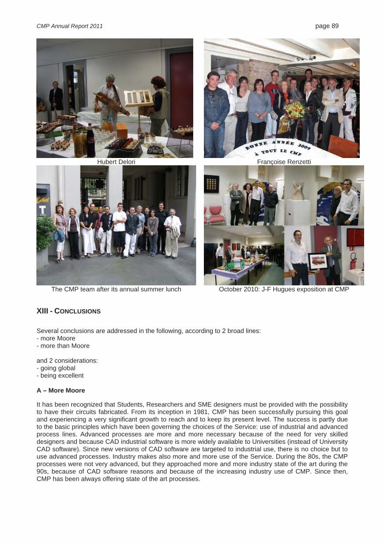
CMP Annual Report 2011 page 89
Hubert Delori Françoise Renzetti
The CMP team after its annual summer lunch October 2010: J-F Hugues exposition at CMP
XIII - CONCLUSIONS Several conclusions are addressed in the following, according to 2 broad lines: - more Moore - more than Moore and 2 considerations: - going global - being excellent A – More Moore It has been recognized that Students, Researchers and SME designers must be provided with the possibility to have their circuits fabricated. From its inception in 1981, CMP has been successfully pursuing this goal and experiencing a very significant growth to reach and to keep its present level. The success is partly due to the basic principles which have been governing the choices of the Service: use of industrial and advanced process lines. Advanced processes are more and more necessary because of the need for very skilled designers and because CAD industrial software is more widely available to Universities (instead of University CAD software). Since new versions of CAD software are targeted to industrial use, there is no choice but to use advanced processes. Industry makes also more and more use of the Service. During the 80s, the CMP processes were not very advanced, but they approached more and more industry state of the art during the 90s, because of CAD software reasons and because of the increasing industry use of CMP. Since then, CMP has been always offering state of the art processes.

CMP Annual Report 2011 page 90 More specifically the following table summarizes the evolution in silicon fabrication and participation during the nineteen last years.
YEAR NB OF CIRCUITS NB OF INSTITUTIONS TECHNOLOGIES
1992
114
38
ES2 1.5 µ, 1.2 µ CMOS TCS Bip AMS 2 µ 2M2P, 1.2 2M2P more integration
1993
197
55
ES2 1.5 µ, 1.2 µ, 1.0 µ CMOS TCS Bip AMS 2 µ 2M2P, 1.2 2M2P, 1.2 µ 2M 2P BiCMOS TCS 0.8 µ Dig. GaAs
more integration
1994
251
75 ES2 1.5 µ, 1.2 µ, 1.0 µ, 0.7 µ CMOS TCS Bip AMS 1.2 µ 2M2P, 1.2 µ 2M 2P BiCMOS 0.8 µ 2M1P VSC 0.6 µ Dig. GaAs STM 0.5 µ TLM
more integration
1995
298
94 ES2 1.2 µ, 1.0 µ, 0.7 µ CMOS TCS Bip AMS 1.2 µ 2M2P, 1.2 µ 2M 2P BiCMOS 0.8 µ 2M2P, 0.8 µ 2M2P BiCMOS VSC 0.6 µ Dig. GaAs PML 0.2 µ HEMT GaAs
more integration
1996
354
107 ES2 1.2 µ, 1.0 µ, 0.7 µ CMOS TCS Bip AMS 1.2 µ 2M2P, 1.2 µ 2M 2P BiCMOS 0.8 µ 2M2P, 0.8 µ 2M2P BiCMOS VSC 0.6 µ Dig. GaAs PML 0.2 µ HEMT GaAs
more integration
1997
333
112 ES2 1.0 µ, 0.7 µ CMOS AMS 1.2 µ 2M2P, 1.2 µ 2M 2P BiCMOS 0.8 µ 2M2P, 0.8 µ 2M2P BiCMOS 0.6 µ 2M 2P VSC 0.6 µ Dig. GaAs PML 0.2 µ HEMT GaAs
more integration
1998
259
94 ES2 0.7 µ CMOS AMS 1.2 µ 2M2P, 1.2 µ 2M 2P BiCMOS 0.8 µ 2M2P, 0.8 µ 2M2P BiCMOS 0.6 µ 2M 2P ST 0.25 µ 6M CMOS VSC 0.5 µ Dig. GaAs PML 0.2 µ HEMT GaAs MCNC MUMPs surface micromachining
more integration
1999
348
100 AMS 1.2 µ , .8 μ, 0.6 μ , 0.35μ CMOS 1.2 µ , 0.8 µ BiCMOS 0.8 µ HBT CMOS (SiGe) ST 0.25 µ CMOS PML 0.2 µ HEMT GaAs CRONOS MUMPs surface micromachining
more integration
2000
305
103
AMS 1.2 µ , 0.8 μ, 0.6 μ , 0.35μ CMOS 0.8 µ BiCMOS 0.8 µ HBT CMOS (SiGe) ST 0.25 µ, 0.18μ CMOS OMMIC 0.2 µ HEMT GaAs CRONOS MUMPs surface micromachining
more integration
2001 277 97 austriamicrosystems 0.8 μ, 0.6 μ , 0.35μ CMOS 0.8 µ BiCMOS 0.8 µ HBT CMOS (SiGe) STMic. 0.25 µ, 0.18μ CMOS Peregrine 0.5µ SOI/SOS CMOS OMMIC 0.2 µ HEMT GaAs CRONOS MUMPs surface micromachining
more integration

CMP Annual Report 2011 page 91
2002 282 89 austriamicrosystems 0.8 μ, 0.6 μ , 0.35μ CMOS 0.8 µ, 0.35µ BiCMOS 0.8 µ HBT CMOS (SiGe) ST. 0.18 µ, 0.12μ CMOS 0.35 µ HBT CMOS (SiGe) Peregrine 0.5µ SOI/SOS CMOS OMMIC 0.2 µ HEMT GaAs CRONOS MUMPs surface micromachining
more integration
2003 283 85 austriamicrosystems 0.8 μ, 0.6 μ , 0.35μ CMOS 0.8 µ, 0.35µ BiCMOS 0.8 µ HBT CMOS (SiGe) ST 0.18 µ, 0.12μ CMOS 0.35 µ SiGe BiCMOS Peregrine 0.5µ SOI/SOS CMOS OMMIC 0.2 µ HEMT GaAs MEMSCAP PolyMUMPs, SOIMUMPs
more integration
2004 260 86 austriamicrosystems 0.8 μ, 0.6 μ , 0.35μ CMOS 0.35μ CMOS-opto, 0.35μ CMOS-RF 0.8 µ BiCMOS 0.35µ SiGe BiCMOS ST 0.18 µ, 0.12μ CMOS 0.35 µ SiGe BiCMOS OMMIC 0.2 µ HEMT GaAs MEMSCAP PolyMUMPs
more integration
2005 262 94 austriamicrosystems 0.6 μ , 0.35μ CMOS 0.35μ CMOS-opto, 0.8 µ BiCMOS 0.35µ SiGe BiCMOS ST 0.18 µ, 0.12μ, 90 nmCMOS 0.35 µ SiGe BiCMOS 0.25 µ SiGe:C BiCMOS OMMIC 0.2 µ HEMT GaAs MEMSCAP PolyMUMPs
more integration
2006 329 93 austriamicrosystems 0.6 μ , 0.35μ CMOS 0.35μ CMOS-opto, CMOS HV, CMOS RF 0.35µ SiGe BiCMOS ST 0.12μCMOS, 90 nmCMOS, 65 nm CMOS 0.35 µ SiGe BiCMOS 0.25 µ SiGe:C BiCMOS CSMC 0.6 μ CMOS OMMIC 0.2 µ HEMT GaAs MEMSCAP PolyMUMPs, SOIMUMPS, MetalMUMPS
more integration
2007 401 105 austriamicrosystems 0.35μ CMOS 0.35μ CMOS-opto, CMOS HV, CMOS RF 0.35µ SiGe , 0.35µ HV EEPROM ST 0.12μCMOS, 90 nmCMOS, 65 nm CMOS 0.35 µ SiGe BiCMOS 0.25 µ SiGe:C BiCMOS
CSMC 0.6 μ CMOS OMMIC 0.2 µ HEMT GaAs MEMSCAP PolyMUMPs, SOIMUMPS, MetalMUMPS CSMC 0.6 μ CMOS Bulkmicromachining
more integration

CMP Annual Report 2011 page 92
2008 375 89 austriamicrosystems 0.35μ CMOS 0.35μ CMOS-opto, CMOS HV, CMOS HV EEPROM, CMOS RF 0.35µ SiGe BiCMOS 0.35µ CMOS bulk micromachining ST CMOS: 130 nm, 90 nm, 65 nm, 45 nm SOI: 130 nm, 65 nm 0.25 µ SiGe:C BiCMOS OMMIC 0.2 µ HEMT GaAs 0.2µ HEMT Bulk micromachining MEMSCAP PolyMUMPs, SOIMUMPS, MetalMUMPS SANDIA SUMMiT V
more integration
2009 391 104 austriamicrosystems 0.35μ CMOS 0.35μ CMOS-opto, CMOS HV, CMOS HV EEPROM, CMOS RF 0.35µ SiGe BiCMOS 0.35µ CMOS bulk micromachining ST CMOS: 130 nm, 90 nm, 65 nm, 40 nm SOI: 130 nm, 65 nm MEMSCAP PolyMUMPs, SOIMUMPS, MetalMUMPS SANDIA SUMMiT V
more integration
2010 354 122 austriamicrosystems 0.35μ CMOS/CMOS-opto, CMOS HV, CMOS HV EEPROM 0.35µ SiGe BiCMOS 0.35µ CMOS bulk micromachining ST CMOS: 130 nm, 65 nm, 40 nm SOI: 130 nm, 65 nm SiGe BiCMOS: 130nm TEZZARON/GLOBALFOUNDRIES 2 Tiers 3D-IC/130nm CMOS CEA-LETI 20 nm FDSOI MEMSCAP PolyMUMPs, SOIMUMPS, MetalMUMPS SANDIA SUMMiT V
more integration
2011
213 96 austriamicrosystems 0.35 µ CMOS /CMOS-Opto 0.35 µ CMOS High Voltage 0.35 µ CMOS RF ThickM4 & MIM 0.35 µ SiGe BiCMOS 0.35 µ CMOS bulk micromachining ST CMOS : 130 nm, 65 nm, 40 nm, 28 nm SOI: 130 nm, 65 nm SiGe BiCMOS: 130 nm TEZZARON/GLOBALFOUNDRIES 2 Tiers 3D-IC/130nm CMOS CEA-LETI 20 nm FDSOI TriQuint Semiconductor 0.15 µ GaAs Dmode p-HEMT MEMSCAP PolyMUMPs, SOIMUMPS, MetalMUMPS
Key issues in 2011 are:
large portfolio of technologies down to 20nm
introduction of a 3D process in cooperation with CMC in Canada and MOSIS in the USA
But cost and acceptance are slowering down the use of ever advanced processes. Practical difficulties are poping up like power density, temperature, variability, leakage power, analog design, etc. The costs are rising high if circuits are not manufactured in very large volumes. A way to overcome the cost issue while keeping costs reasonable is to go for larger die sizes on current-generation geometrics. But anyway fundamental limits coming from thermodynamics, quantum mechanics, electromagnetics, … will set show stoppers sooner or later.

CMP Annual Report 2011 page 93 fundamental limits coming from thermodynamics, quantum mechanics, electromagnetics, … will set show stoppers sooner or later. B - More than Moore The quest for always larger densities may also be satisfied with 3D integration, possibly not including very advanced process dies for cost reasons. System in package integration (SiP) allows heterogeneous integration, like sensors, electronics, etc. opposed to systems on chip (SoC) in which all parts are manufactured on the same process, which is not always optimal. 3D processes using TSVs (Through Silicon Vias) allow to go one step further: interconnections are shorter, hence leading to power savings and better performance, there are less I/Os so less power is consumed. Heterogeneous integration is also possible as for SiP. There are still concerns to be addressed like thermal issues (increased density may lead to hot spots, electromigration,….), power (no power savings if current-generation geometrics are used), CAD software. CMP has introduceda 3D processe using TSVs in 2010. A step further may be required for some applications where the substrate is required to be flexible, like for many BioMed applications. Organic electronics allow 3D integration as well, for a cheap cost, for large areas, for heterogeneous integration. Biocompatibility is also a plus for BioMed applications. B. KAMINSKA et al. have introduced a good example of such systems. A multilayer polymer microsensor system allows skin tissue conformity since the substrate can bend up to 30°. It includes various sensors, signal conditioning, processing, RF communication, powering from disposable or rechargeable batteries. The prototype includes electrodes for ECG and a MEMS accelerometer for body positioning calculation. It is also recognized that complementary developments must be addressed, in order to address more diversified needs. With this respect, CMP has been a pioneer in being the first service in the world to offer MEMS processes as early as 1995. Going further, more than mechanics-electronics is to be addressed like photonics, optics, fluidics, etc. CMP will be actively promoting these developments in the future (see Appendices 18 and 19). C - Going global The cooperation between service organizations has already been mentioned. On the side of the users of CMP and of other similar services, the design way is also going more and more global in the sense that more and more IP blocks may come from various sources. This is due to the ever increasing complexity of designs, including parts coming from various teams, countries, companies, etc. An initiative is being developed to go this way: the Global Education for Microelectronic Systems (GEMS). D - Being excellent Globalization also requires to be excellent in order to stay ahead of others. This is important at the time of global markets, when every country or continent is a high cost country or continent to another one. Some countries or continents that were said to be “low-cost” countries or continents a few years ago already experience that other countries or continents are coming to the picture with lower costs, forcing them to outsource their own outsourcing. The way to combat that is to stay ahead of the others. The way to stay ahead is to educate and research using top level electronic processes available from top level services like CMP. BIBLIOGRAPHY KAMINSKA B., CHUO Y. “Multiparameter Single Locus Integrated Multilayer Polymer Microsensor System”, to appear in IEEE Trans. on BIOCaS. RUCINSKI A. “Global Education for Microelectronic Systems, www.ieee-gems.edu” India outsources its own outsourcing – Pioneer nation fends off new rivals, International Herald Tribune – 25 September 2007


APPENDICES
1) Overview of the different technologies
2) Participation per Institution in 2011
3) New participants in 2011
4) Institutions having submitted circuits for Industry in 2011
5) Low volume production in 2011
6) Educational circuits, France, 2011
7) Institutions having submitted circuits 1981 - 2011
8) History of CMP projects 1981 - 2011
9) Design kits at CMP
10) Turnaround time of the 2011 projects
11) Annual users’ meeting participants
12) Announcements
13) Press Release: CMC, CMP and MOSIS to increase cooperation for delivery of better technology
14) Communiqué
15) Press Articles 2010-2011
16) Grenoble’s environment
17) Protocol issued from the 2-3 October 1986 meeting
18) Quality Assurance
19) Examples of MEMS for BioMed applications
20) Electronics for energy management
21) Contact persons


APPENDIX 1: Overview of the different technologies
The following technologies are available for prototyping and low volume production. Integrated Circuits 0.18 µ C18 CMOS 6LM austriamicrosystems 0.18 µ H18 High Voltage CMOS 6LM austriamicrosystems 0.35 µ C35B4C2 CMOS DLP/4LM 3.3V austriamicrosystems 0.35 µ C35B4C3 CMOS DLP/4LM 3.3V/5.0V austriamicrosystems 0.35 µ C35B4O1 CMOS-Opto DLP/4LM austriamicrosystems 0.35 µ C35B4M3 CMOS DLP/4LM ThickM4 & MIM austriamicrosystems 0.35 µ H35B4D3 CMOS DLP/4LM High Voltage austriamicrosystems 0.35 µ C35B4E3 CMOS DLP/4LM EEPROM / Flash austriamicrosystems 0.35 µ S35D4M5 SiGe BiCMOS DLP/4LM austriamicrosystems 28 nm CMOS28LP CMOS 7LM STMicroelectronics 40 nm CMOS040 CMOS 7LM STMicroelectronics 65 nm CMOS065 CMOS 7LM STMicroelectronics 65 nm CMOS065-SOI SOI 6LM STMicroelectronics 130 nm HCMOS9GP CMOS 6LM STMicroelectronics 130 nm BiCMOS9MW SiGe BiCMOS 6LM STMicroelectronics 130 nm HCMOS9-SOI SOI 6LM STMicroelectronics 0.15 µ TQP15 GaAs Dmode p-HEMT 2LM TriQuint semiconductor 20 nm FDSOI FDSOI 4LM LETI-CEA
Micro Electro Mechanical Systems (MEMS) PolyMUMPs PolyMUMPs MEMSCAP SOIMUMPs SOIMUMPs MEMSCAP MetalMUMPs MetalMUMPs MEMSCAP Bulk Micromachining CMOS DLP/4LM + Post Process austriamicrosystems + Post Process
3D Integrated Circuits (3D-IC) 130nm CMOS FaStack 130nm 2 Tiers 3D-IC Tezzaron/GlobalFoundries

TECHNOLOGY: CMOS 0.18 µ C18 Met. layer(s): 6 metal layers / Thick Metal6 Capacitors: Single MiM / Dual MiM / High density MiM Maximum die size: 2cm x 2cm
Standard cells: digital standard cells and IO pads analog standard cells and IO pads
Available I/O: I/O cell library with available for 1.8V/5V. Temp. range: -40° C. / +180° C. Supply voltage: 1.8V, 5.0V SPECIAL FEATURES: High performance mixed analog/digital applications APPLICATION AREA: Mixed signal analog digital, system on chip LIBRARIES: Digital cells: Standard digital cells and IO pads. Megacells: RAM, ROM, FIFO can be generated by the foundry on request with additional fees. RAM/DP-RAM: Available on request DESIGN KITS: Workstation based: CADENCE, SYNOPSYS, MENTOR PC based: None PACKAGING: All standard packages (DIL, LCC, PGA,...). TEST: Contact CMP INTERFACE FORMAT: GDSII SPICE parameters: SPECTRE, HSPICE DRC, ERC rule set: Assura, Calibre DESIGN SUPPORT: Only DRC checking (free for submitted designs) PRICES: Cell libraries: Available for free Design kits: Available for free Prototyping: See the general CMP price list for prototyping Low volume production: Depends on each specific case; contact CMP TURNAROUND TIME: Typical: 13 weeks (from GDS2 tape to packaged parts). TECHNOLOGY: CMOS 0.18 µ H18 Met. layer(s): 6 metal layers / Thick Metal6 Capacitors: Single MiM / Dual MiM / High density MiM Maximum die size: 2cm x 2cm
Standard cells: digital standard cells and IO pads analog standard cells and IO pads
Available I/O: I/O cell library with available for 1.8V/5V. High Voltage IO pads for 20V or 50V
Temp. range: -40° C. / +180° C. Supply voltage: 1.8V, 5.0V, 20V, 50V (max gate voltage 20V) SPECIAL FEATURES: High performance analog/digital/High-Voltage applications APPLICATION AREA: Mixed signal analog digital, HV designs, system on chip LIBRARIES: Digital cells: Standard digital cells with the same in floating cells version. Megacells: RAM, ROM, FIFO can be generated by the foundry on request with additional fees. RAM/DP-RAM: Available on request DESIGN KITS: Workstation based: CADENCE, SYNOPSYS, MENTOR PC based: None PACKAGING: All standard packages (DIL, LCC, PGA,...). TEST: Contact CMP INTERFACE FORMAT: GDSII SPICE parameters: SPECTRE, HSPICE DRC, ERC rule set: Assura, Calibre DESIGN SUPPORT: Only DRC checking (free for submitted designs) PRICES: Cell libraries: Available for free Design kits: Available for free Prototyping: See the general CMP price list for prototyping Low volume production: Depends on each specific case; contact CMP TURNAROUND TIME: Typical: 13 weeks (from GDS2 tape to packaged parts).

TECHNOLOGY: CMOS 0.35 µ C35B4C2 Met. layer(s): 4 Poly layer(s): 2, high resistive poly Maximum die size: 2cm x 2cm Usable cells: about 300 digital cells Available I/O: I/O cell library with digital pads is available 3.3V Temp. range: -40° C. / +125° C. Supply voltage: 3.3V SPECIAL FEATURES: High performance analog/digital process APPLICATION AREA: Mixed signal analog digital, large digital designs, system on chip LIBRARIES: Digital cells: All the standard digital cells plus composed cells (complex gates, shift registers,...). Megacells: RAM, ROM, FIFO can be generated by the foundry on request with additional fees. RAM/DP-RAM: Predefined RAM/DP-RAM, free of charge for Education and Research. See Configurations. DESIGN KITS: Workstation based: CADENCE, SYNOPSYS, MENTOR PC based: TANNER PACKAGING: All standard packages (DIL, LCC, PGA,...). TEST: Contact CMP INTERFACE FORMAT: GDSII, CIF, CADENCE SPICE parameters: SPECTRE, HSPICE, ELDO, SABER, SMASH, PSPICE DRC, ERC rule set: Diva, Assura, Calibre, Tanner DESIGN SUPPORT: Only DRC checking (free for submitted designs), extended ERC on request PRICES: Cell libraries: Distributed for free by CMP for dig. cells Design kits: Distributed for free by CMP for dig. cells Prototyping: See the general CMP price list for prototyping Low volume production: Depends on each specific case; contact CMP TURNAROUND TIME: Typical: 11 weeks (from GDS2 tape to packaged parts)
TECHNOLOGY: 0.35 µ CMOS C35B4C3 Met. layer(s): 4 Poly layer(s): 2, high resistive poly Maximum die size: 2cm x 2cm Usable cells: about 300 digital cells Available I/O: I/O cell library with digital pads is available 3V, 3V/5V, 5V with internal level shifters Temp. range: -40° C. / +125° C. Supply voltage: 5V or 3.3V SPECIAL FEATURES: High performance analog/digital process APPLICATION AREA: Mixed signal analog digital, large digital designs, system on chip LIBRARIES: Digital cells: All the standard digital cells plus composed cells (complex gates, shift registers,...). Megacells: RAM, ROM, FIFO can be generated by the foundry on request with additional fees. RAM/DP-RAM: Predefined RAM/DP-RAM, free of charge for Education and Research. See Configurations. DESIGN KITS: Workstation based: CADENCE, SYNOPSYS, MENTOR PC based: TANNER PACKAGING: All standard packages (DIL, LCC, PGA,...). TEST: Contact CMP INTERFACE FORMAT: GDSII, CADENCE SPICE parameters: SPECTRE, HSPICE, ELDO, SABER, SMASH, PSPICE DRC, ERC rule set: Diva, Assura, Calibre, Tanner DESIGN SUPPORT: Only DRC checking (free for submitted designs), extended ERC on request PRICES: Cell libraries: Distributed for free by CMP for dig. cells Design kits: Distributed for free by CMP for dig. cells Prototyping: See the general CMP price list for prototyping Low volume production: Depends on each specific case; contact CMP TURNAROUND TIME: Typical: 11 weeks (from GDS2 tape to packaged parts).
TECHNOLOGY: 0.35 µ CMOS-Opto C35B4O1 This 0.35 CMOS-Opto process is offered in each 0.35 CMOS run (C35B4C3). The C35B4O1 is with 4 layers metal available for prototyping and low volume production.
Met. layer(s): 4 Poly layer(s): 2 Maximum die size: 2cm x 2cm Usable cells: about 300 digital cells Available I/O: I/O cell library with digital pads is available 3V, 3V/5V, 5V with internal level shifters Temp. range: -40° C. / +125° C. Supply voltage: 5V or 3.3V SPECIAL FEATURES: See the Process Datasheet. APPLICATION AREA: Provides enhanced optical sensitivity for embedded photodiodes and high density CMOS camera products. LIBRARIES: Digital cells: All the standard digital cells plus composed cells (complex gates, shift registers,...). Megacells: RAM, ROM, FIFO can be generated by the foundry on request with additional fees.
RAM/DP-RAM: Predefined RAM/DP-RAM, free of charge for Education and Research. See Configurations.
DESIGN KITS: Workstation based: CADENCE, SYNOPSYS, MENTOR PC based: TANNER PACKAGING: All standard packages (DIL, LCC, PGA,...). TEST: Contact CMP. INTERFACE FORMAT: GDSII, CADENCE. SPICE parameters: SPECTRE, HSPICE, ELDO, SABER, SMASH, PSPICE. DRC, ERC rule set: Diva, Assura, Calibre, Tanner DESIGN SUPPORT: Only DRC checking (free for submitted designs), extended ERC on request. PRICES: Cell libraries: Distributed for free by CMP for dig. cells. Design kits: Distributed for free by CMP for dig. cells. Prototyping: See the general CMP price list for prototyping. Low volume production: Depends on each specific case; contact CMP. TURNAROUND TIME: Typical: 11 weeks (from GDS2 tape to packaged parts).
TECHNOLOGY: 0.35 µ CMOS C35B4M3 Same as C35B4C3 with Thick Metal module instead of Metal 4 module and with MIM capacitor module
Poly layer(s): 2, high resistive poly Maximum die size: 2cm x 2cm Usable cells: about 300 digital cells Available I/O: I/O cell library with digital pads is available 3V, 3V/5V, 5V with internal level shifters Temp. range: -40° C. / +125° C. Supply voltage: 5V or 3.3V SPECIAL FEATURES: High performance analog/digital/RF process APPLICATION AREA: Mixed signal analog digital, large digital designs, system on chip, RF. LIBRARIES: Digital cells: All the standard digital cells plus composed cells (complex gates, shift registers,...). Megacells: RAM, ROM, FIFO can be generated by the foundry on request with additional fees. RAM/DP-RAM: Predefined RAM/DP-RAM, free of charge for Education and Research. See Configurations. DESIGN KITS: Workstation based: CADENCE, SYNOPSYS, MENTOR PC based: - PACKAGING: All standard packages (DIL, LCC, PGA,...). TEST: Contact CMP INTERFACE FORMAT: GDSII, CADENCE SPICE parameters: SPECTRE, HSPICE, ELDO, SABER, SMASH, PSPICE DRC, ERC rule set: Diva, Assura, Calibre DESIGN SUPPORT: Only DRC checking (free for submitted designs), extended ERC on request PRICES: Cell libraries: Distributed for free by CMP for dig. cells Design kits: Distributed for free by CMP for dig. cells Prototyping: See the general CMP price list for prototyping Low volume production: Depends on each specific case; contact CMP TURNAROUND TIME: Typical: 13 weeks (from GDS2 tape to packaged parts).

TECHNOLOGY: 0.35 µ CMOS H35B4D3 Met. layer(s): 4, Thick Metal4 Poly layer(s): 2, high resistive poly Maximum die size: 2cm x 2cm Usable cells: about 300 digital cells
Available I/O: I/O cell library with digital pads is available 3V, 3V/5V, 5V with internal level shifters. Floating digital pads available with 3.3V
Temp. range: -40° C. / +125° C. Supply voltage: 5V, 3.3V, 20V, Max operating voltage 50V (max gate voltage 5V, 20V)
SPECIAL FEATURES: High performance analog/digital/HV process
APPLICATION AREA: Mixed signal analog digital, HV designs, system on chip LIBRARIES:
Digital cells: All the standard digital cells plus composed cells (complex gates, shift registers,...), with the same in floating cells version.
Megacells: RAM, ROM, FIFO can be generated by the foundry on request with additional fees. RAM/DP-RAM: Predefined RAM/DP-RAM, free of charge for Education and Research. See Configurations. DESIGN KITS: Workstation based: CADENCE, SYNOPSYS, MENTOR PC based: PACKAGING: All standard packages (DIL, LCC, PGA,...). TEST: Contact CMP INTERFACE FORMAT: GDSII, CADENCE SPICE parameters: SPECTRE, HSPICE, ELDO DRC, ERC rule set: Assura, Calibre DESIGN SUPPORT: Only DRC checking (free for submitted designs), extended ERC on request PRICES: Cell libraries: Distributed for free by CMP for dig. cells Design kits: Distributed for free by CMP for dig. cells Prototyping: See the general CMP price list for prototyping Low volume production: Depends on each specific case; contact CMP TURNAROUND TIME: Typical: 13 weeks (from GDS2 tape to packaged parts).
TECHNOLOGY: 0.35 µ CMOS C35B4E3 Embedded Flash Met. layer(s): 4 Poly layer(s): 2 Maximum die size: 2cm x 2cm Usable cells: about 300 digital cells Available I/O: I/O cell library with digital pads is available 3V, 3V/5V, 5V with internal level shifters Temp. range: -40° C. / +125° C. Supply voltage: 5V or 3.3V SPECIAL FEATURES: High performance analog/digital process embedding Flash/EEPROM The process is fully compatible with C35B4C3 APPLICATION AREA: Mixed signal analog digital, large digital designs, system on chip LIBRARIES: Digital cells: All the standard digital cells plus composed cells (complex gates, shift registers,...). Megacells: RAM, ROM, FIFO can be generated by the foundry on request with additional fees. RAM/DP-RAM: Predefined RAM/DP-RAM, free of charge for Education and Research. See Configurations. Flash/EEPROM 4K x 16 Synchronous EEPROM block (32K x 8 available Q2-2006) DESIGN KITS: Workstation based: CADENCE, SYNOPSYS, MENTOR PC based: TANNER PACKAGING: All standard packages (DIL, LCC, PGA,...). TEST: Contact CMP INTERFACE FORMAT: GDSII, CADENCE SPICE parameters: SPECTRE, HSPICE, ELDO, SABER, SMASH, PSPICE DRC, ERC rule set: Diva, Assura, Calibre, Tanner DESIGN SUPPORT: Only DRC checking (free for submitted designs), extended ERC on request PRICES: Cell libraries: Distributed for free by CMP for dig. cells Design kits: Distributed for free by CMP for dig. cells Flash/EEPROM Available with additional fees Prototyping: See the general CMP price list for prototyping Low volume production: Depends on each specific case; contact CMP TURNAROUND TIME: 11 weeks (from GDS2 tape to packaged parts).

TECHNOLOGY: 0.35 µ SiGe BiCMOS S35D4M5 from austriamicrosystems Met. layer(s): 4, thick metal, MIM capacitor Poly layer(s): 2, high resistive poly. Maximum die size: 2cm x 2cm Usable cells: about 300 digital cells Available I/O: I/O cell library with digital pads is available 3V, 3V/5V, 5V with internal level shifters Temp. range: -40° C. / +125° C. Supply voltage: 5V or 3.3V SPECIAL FEATURES: High performance analog/RF/digital process APPLICATION AREA: Mixed signal analog/RF/digital, large digital designs, system on chip LIBRARIES: Digital cells: All the standard digital cells plus composed cells (complex gates, shift registers,...). Megacells: RAM, ROM, FIFO can be generated by the foundry on request with additional fees. RAM/DP-RAM: Predefined RAM/DP-RAM, free of charge for Education and Research. See Configurations. DESIGN KITS: Workstation based: CADENCE, SYNOPSYS PC based: - PACKAGING: All standard packages (DIL, LCC, PGA,...). TEST: Contact CMP INTERFACE FORMAT: GDSII, CADENCE SPICE parameters: SPECTRE, HSPICE, ELDO, SABER, SMASH, PSPICE DRC, ERC rule set: DIVA, ASSURA, CALIBRE DESIGN SUPPORT: Only DRC checking (free for submitted designs), extended ERC on request PRICES: Cell libraries: Distributed for free by CMP for dig. cells Design kits: Distributed for free by CMP for dig. cells Prototyping: See the general CMP price list for prototyping Low volume production: Depends on each specific case; contact CMP TURNAROUND TIME: Typical: 13 weeks (from GDS2 tape to packaged parts).
TECHNOLOGY: CMOS 28nm (CMOS28LP) from STMicroelectronics
Spec. process char.:
Gate length : 28nm drawn poly length Dual or triple Vt MOS transistors Dual or triple gate oxide Dual-damascene copper for interconnect. 8 metal layers for interconnect. 0.1um metallization pitch. Various power supplies supported : 1.8V, 1.0V Embedded memory (Single port RAM / ROM / Double Port RAM )
CAD TOOLS:
Workstation based: The design kits are supported under Cadence for full-custom analog / RF: Virtuoso, Eldo, Spectre, Hspice & Layout-XL & ICC. DRC/LVS are supported under Mentor / Calibre.
LIBRARIES: Standard-cells design flows are supported under Cadence's SOC Encounter or Synopsys Design-Compiler / Physical Compiler.
PACKAGING: All standard packages (DIL, LCC, PGA,...) TEST: Contact CMP INTERFACE FORMAT: GDSII, CADENCE SPICE parameters: SPECTRE, ELDO, HSPICE DESIGN SUPPORT: DRC checking (free for submitted designs) PRICES: Cell libraries: Distributed for free by CMP Design kits: Distributed for free by CMP Prototyping: See the general CMP price list for prototyping TURNAROUND TIME: Typical: 16 weeks (from GDS2 tape to packaged parts)

TECHNOLOGY: CMOS 40nm (CMOS040) from STMicroelectronics
Spec. process char.:
Gate length : 45nm drawn poly length Dual or triple Vt MOS transistors Dual or triple gate oxide Dedicated process flavors for high performance or low power Dual-damascene copper for interconnect. 7 metal layers for interconnect. 0.14um metallization pitch. Various power supplies supported : 1.8V, 1.1V, 0.9V Triple standard cell libraries (more than 1.6 Mgates/mm2). Embedded memory (Single port RAM / ROM / Double Port RAM
CAD TOOLS:
Workstation based: The design kits are supported under Cadence for full-custom analog / RF: Analog-Artist, Composer, Eldo, Spectre, NCSim, Virtuoso & Layout-XL & ICC. DRC/LVS are supported under Mentor / Calibre.
LIBRARIES: Standard-cells design flows are supported under Cadence's SOC Encounter or Synopsys Design-Compiler / Physical Compiler.
PACKAGING: All standard packages (DIL, LCC, PGA,...) TEST: Contact CMP INTERFACE FORMAT: GDSII, CADENCE SPICE parameters: SPECTRE, ELDO, HSPICE DESIGN SUPPORT: DRC checking (free for submitted designs), and extended ERC on digital/mixed A/D designs PRICES: Cell libraries: Distributed for free by CMP Design kits: Distributed for free by CMP Prototyping: See the general CMP price list for prototyping TURNAROUND TIME: Typical: 16 weeks (from GDS2 tape to packaged parts) TECHNOLOGY: CMOS 65nm (CMOS065) from STMicroelectronics
Spec. process char.:
Gate length : 65nm drawn poly length Dual or triple Vt MOS transistors Dual or triple gate oxide Dedicated process flavors for high performance or low power Dual-damascene copper for interconnect. Low-k (k = 2.9) dielectric. 6 or 7 metal layers dor interconnect. 0.20um metallization pitch. Analog / RF capabilities. Various power supplies supported : 2.5V, 1.8V, 1.2V, 1V Triple standard cell libraries (more than 800kgates/mm2). Embedded memory (Single port RAM / ROM / Double Port RAM
CAD TOOLS:
Workstation based: The design kits are supported under Cadence for full-custom analog / RF: Analog-Artist, Composer, Eldo, Spectre, NCSim, Virtuoso & Layout-XL & ICC. DRC/LVS are supported under Mentor / Calibre.
LIBRARIES: Standard-cells design flows are supported under Cadence's SOC Encounter or Synopsys Design-Compiler / Physical Compiler.
PACKAGING: All standard packages (DIL, LCC, PGA,...) TEST: Contact CMP INTERFACE FORMAT: GDSII, CADENCE SPICE parameters: SPECTRE, ELDO, HSPICE DESIGN SUPPORT: DRC checking (free for submitted designs), and extended ERC on digital/mixed A/D designs PRICES: Cell libraries: Distributed for free by CMP Design kits: Distributed for free by CMP Prototyping: See the general CMP price list for prototyping TURNAROUND TIME: Typical: 16 weeks (from GDS2 tape to packaged parts) TECHNOLOGY: SOI CMOS 65nm (CMOS065-SOI) from STMicroelectronics
Spec. process char.:
Gate length : 65nm drawn poly length Triple-VT 1.2V transistors, with both floating body and Body-contacted versions Partially Depleted SOI on High Resistivity Substrate 6 layers metal Cu, (last metal is thick). Thick top metal 0.20um metallization pitch. Analog / RF capabilities. RF-MOS, RF-PADS, varactors, inductors.
CAD TOOLS:
Workstation based: The design kits are supported under Cadence for full-custom analog / RF: Analog-Artist, Composer, Eldo, Spectre, NCSim, Virtuoso & Layout-XL & ICC. DRC/LVS are supported under Mentor / Calibre.
LIBRARIES: Standard-cells design flows are supported under Cadence's SOC Encounter or Synopsys Design-Compiler / Physical Compiler.
PACKAGING: All standard packages (DIL, LCC, PGA,...)

TEST: Contact CMP INTERFACE FORMAT: GDSII, CADENCE SPICE parameters: SPECTRE, ELDO, HSPICE DESIGN SUPPORT: DRC checking (free for submitted designs), and extended ERC on digital/mixed A/D designs PRICES: Cell libraries: Distributed for free by CMP Design kits: Distributed for free by CMP Prototyping: See the general CMP price list for prototyping TURNAROUND TIME: Typical: 16 weeks (from GDS2 tape to packaged parts)
TECHNOLOGY: CMOS 130 nm (HCMOS9GP) from STMicroelectronics
Spec. process char.:
Gate length : .13mic (drawn), 130 nm (effective) Triple well Power supply 1.2 V Multiple Vt transistor offering (low leakage, standard, High speed) Threshold voltages (for 3 families above) : VTN = 570/500/380 mV, VTP = 590/480/390 mV Isat (for 3 families above) : TN @ 1.2 V : 410/535/680 uA/mic; TP @ 1.2 V : 170/240/320 uA/mic 6 metal layers in standard. Up to 8 metal layers in option Low k inter-level dielectric MIM capacitances 2.5V power supply option is also available WARNING: the 3.3V-transistors option and the ULL option are no longer be available since January 2007
CAD TOOLS:
Workstation based: CADENCE, SYNOPSYS Full custom designs are supported using Virtuoso layout. The layout verifications (DRC, ERC, extraction, LVS) are fully supported for Calibre. Transistor-level simulations are supported under Spectre and Eldo
LIBRARIES: Standard-cell designs are supported using Verilog/VHDL descriptions for synthesis and simulation. Synthesis is supported under Synopsys. Simulation is supported under Verilog-XL, Leapfrog NCSIM and ModelSim. The automatic place&route is supported under Cadence and Synopsys
PACKAGING: All standard packages (DIL, LCC, PGA,...) TEST: Contact CMP INTERFACE FORMAT: GDSII, CADENCE SPICE parameters: SPECTRE, ELDO DESIGN SUPPORT: DRC checking (free for submitted designs), and extended ERC on digital/mixed A/D designs PRICES: Cell libraries: Distributed for free by CMP Design kits: Distributed for free by CMP Prototyping: See the general CMP price list for prototyping TURNAROUND TIME: Typical: 16 weeks (from GDS2 tape to packaged parts) TECHNOLOGY: BiCMOS SiGe 130 nm (BiCMOS9MW) from STMicroelectronics
Spec. process char.:
CMOS Gate length: 130nm (drawn), 130nm (effective) Triple well Power supply 1.2V Multiple Vt transistor offering (Low Leakage , High Speed) Threshold voltages (for 2 families above): VTN = 450/340mV, VTP = 395/300mV Isat (for 2 families above): TN @ 1.2V: 535/670uA/mic; TP @ 1.2V: 240/310uA/mic Bipolar SiGe transistors: High Speed NPN, Medium Voltage NPN Typical beta (for 2 families above): 1000/1000 Typical Ft (for 2 families above): 230/150GHz 6 metal layers in standard Low k inter-level dielectric MIM capacitances 2.5V-transistors option is also available
CAD TOOLS:
Workstation based: CADENCE, SYNOPSYS Full custom designs are supported using Virtuoso layout. The layout verifications (DRC, ERC, extraction, LVS) are fully supported for Calibre. Transistor-level simulations are supported under Spectre and Eldo
LIBRARIES: Standard-cell designs are supported using Verilog/VHDL descriptions for synthesis and simulation. Synthesis is supported under Synopsys. Simulation is supported under Verilog-XL, Leapfrog NCSIM and ModelSim. The automatic place&route is supported under Cadence and Synopsys.
PACKAGING: All standard packages (DIL, LCC, PGA,...) TEST: Contact CMP INTERFACE FORMAT: GDSII, CADENCE SPICE parameters: SPECTRE, ELDO DESIGN SUPPORT: DRC checking (free for submitted designs), and extended ERC on digital/mixed A/D designs PRICES: Cell libraries: Distributed for free by CMP Design kits: Distributed for free by CMP Prototyping: See the general CMP price list for prototyping

TURNAROUND TIME: Typical: 18 weeks (from GDS2 tape to packaged parts) TECHNOLOGY: SOI CMOS 130 nm (HCMOS9-SOI) from STMicroelectronics
Spec. process char.:
Gate length : 130 nm (drawn), 110 nm (effective) 200 mm SOI wafers with high resistive substrate Power supply : 2.5 V 6 layers metal Cu MIM capacitors Thick top metal CORE and IO libraries
CAD TOOLS:
Workstation based: CADENCE, SYNOPSYS Full custom designs are supported using Virtuoso layout. The layout verifications (DRC, ERC, extraction, LVS) are fully supported for Calibre. Transistor-level simulations are supported under Spectre and Eldo
LIBRARIES: Standard-cells design flows are supported under Cadence's SOC Encounter or Synopsys Design-Compiler / Physical Compiler.
PACKAGING: All standard packages (DIL, LCC, PGA,...) TEST: Contact CMP INTERFACE FORMAT: GDSII, CADENCE SPICE parameters: SPECTRE, ELDO DESIGN SUPPORT: DRC checking (free for submitted designs), and extended ERC on digital/mixed A/D designs PRICES: Cell libraries: Distributed for free by CMP Design kits: Distributed for free by CMP Prototyping: See the general CMP price list for prototyping TURNAROUND TIME: Typical: 12 weeks (from GDS2 tape to packaged parts) TECHNOLOGY: TQP15 GaAs 150nm (D-mode pHEMT) from TriQuint Semiconductor
Spec. process char.:
pHEMT gate length: 150nm power supply 3.0V Pinchoff voltage -1.00V Breakdown Vdg 14V Ft (peak) 80GHz Imax 580mA/mm Gm @ Idss 550 mS/mm Schottky diodes 2 metal layers for interconnects (4µm thick for global, less than 1µm for local) High-Q passives High value MIM capacitors (620pF/mm²) Inductors Thin film resistors Backside vias Die thickness 100µm (4mils) Fixed size for dies with fixed orientation for transistor gates
CAD TOOLS: Workstation based: CADENCE, ADS PC based: ADS, AWR, ICED LIBRARIES: Standard components : pHEMTs, diodes, capacitors, resistors, inductors, backside vias, pads PACKAGING: All standard packages (QFN, LCC, CQFP,...) TEST: Contact CMP INTERFACE FORMAT: GDSII Simulation: TOM3 model for HEMTs, linear and nonlinear models and simulators DESIGN SUPPORT: DRC checking (free for submitted designs) PRICES: Cell libraries: Distributed for free by TriQuint Design kits: Distributed for free by Triquint Prototyping: See the general CMP price list for prototyping TURNAROUND TIME: Typical: 9 weeks (from GDS2 tape to packaged parts)

CEA-LETI R&D 20nm Fully Depleted SOI Multi-Project Wafers – 1st run For years, LETI has pioneered the development of Fully-depleted Silicon on Insulator (FDSOI) technology, demonstrating the advantages of this technology over bulk conventional technology for future nodes. In particular, excellent electrostatic integrity of the transistors is ensured by the thinness of the body, without the need of extra litho steps or channel doping. This leads to a planar device technology that exhibits excellent short channel behavior and record variability results, as shown in a number of recent papers. With this Multi-Project Wafers (MPW) initiative, LETI offers through CMP to the R&D design community the opportunity to implement innovative designs on this technology.
Specific acceptance rules • No commercial products • No military or medical application circuits
Main technology features
• High-k / metal gate stack • Transistor gate lengths down to 25nm • 4 levels of metallization with 65nm ground rules • Single threshold voltage n- and p-MOSFETs with balanced Vth of ±0.4V
Schedule of the first MPW run
• Mid-January 2011: Delivery of the PDK by CMP. The associated documentation is listed below. • End of February 2011: Release of the PDK, including parasitics extraction and place & route flow. • End of Q3 2011: GDS to be delivered to CMP. Setup of the reticle. • First silicon is expected end of Q1 2012.
PDK content and associated documentation
• FDSOI compact model with typical and corners model cards (Compact Model User Manual), • Parameterized cells and pads for the physical implementation • Physical verification files for DRC/LVS (Design Rules Manual), • Characterized Digital Standard cells library (40 cells) • PDK Reference Manual • Design Rules Manual

Technology
PolyMUMPs from MEMSCAP.
Fixed die size:
1cm x 1cm
Special Features
Polysilicon Surface Micomachining. One poly ground layer, two structural poly layers, one gold metal layer, two oxide release layers. Further information : PolyMUMPs overview PolyMUMPs datasheet
Application Area
MEMS, micromechanics, MOEMS.
Libraries
CaMEL (Consolidated Micromechanical Element Library). CaMEL contains a non-parameterized cell database and a parameterized MEMS element library, for use by both the novice and advanced MEMS designers. Both libraries are intended to assist users in the design and layout of MEMS devices by providing an initial layout for components of a MEMS system.
Design Kits
Workstation based: CADENCE, MENTOR GRAPHICS PC based: TANNER
Packaging
Ceramic standard packages (DIL, LCC, PGA,...). No plastic package. Special prices (upon request). Hybrid packaging possible (IC and MEMS in the same package).
Test
Contact CMP
Interface format
GDSII
DRC
CADENCE
Design Support
Only DRC checking (free for submitted designs).
Prices
Cell libraries: Distributed for free by CMP Design kits: Distributed for free by CMP Prototyping: See the general CMP price list for prototyping Low volume production: Depends on each specific case; contact CMP
Turnaround Time
Typical: 10 weeks (from GDS2 tape to naked dies).

Technology
SOIMUMPs from MEMSCAP.
Fixed die size:
0,9cm x 0,9cm
Special Features
DRIE (Deep Reactive Ion Etching) on Silicon-On-Insulator wafer. Further information : SOIMUMPs overview SOIMUMPs datasheet
Application Area
MEMS, micromechanics, MOEMS
Design Kits Workstation based: CADENCE, MENTOR GRAPHICS PC based: TANNER CMP provides a CAD Tool for MEMS design : SoftMEMS
Packaging
Ceramic standard packages (DIL, LCC, PGA,...). No plastic package. Special prices (upon request). Hybrid packaging possible (IC and MEMS in the same package).
Test
Contact CMP
Interface format
GDSII
DRC
CADENCE
Design Support
Only DRC checking (free for submitted designs)
Prices
Cell libraries: Distributed for free by CMP Design kits: Distributed for free by CMP Prototyping: See the general CMP price list for prototyping Low volume production: Depends on each specific case; contact CMP
Turnaround Time
Typical: 10 weeks (from GDS2 tape to naked dies).

Technology
MetalMUMPs from MEMSCAP.
Fixed die size:
1cm x 1cm
Special Features
Electroplated nickel surface micromachining process, thick layers. Further information : MetalMUMPs overview MetalMUMPs datasheet
Application Area
MEMS, micromechanics, MOEMS
Design Kits Workstation based: CADENCE, MENTOR GRAPHICS PC based: TANNER CMP provides a CAD Tool for MEMS design: SoftMEMS
Packaging
Ceramic standard packages (DIL, LCC, PGA,...). No plastic package. Special prices (upon request). Hybrid packaging possible (IC and MEMS in the same package).
Test
Contact CMP
Interface format
GDSII
DRC
CADENCE
Design Support
Only DRC checking (free for submitted designs)
Prices
Cell libraries: Distributed for free by CMP Design kits: Distributed for free by CMP Prototyping: See the general CMP price list for prototyping Low volume production: Depends on each specific case; contact CMP
Turnaround Time
Typical: 10 weeks (from GDS2 tape to naked dies).

Technology
0.35 µm Bulk Micromachining.
Die size:
Minimum charge of 3 mm²
Special Features
0.35 µm CMOS process from austriamicrosystems + TMAH post process etching No additional mask for the MEMS post process Bulk Micromachining announcement
Application Area
MEMS, micromechanics, MOEMS.
Design Kits
Workstation based: CADENCE, MENTOR GRAPHICS, SYNOPSYS PC based: TANNER CMP provides a CAD Tool for MEMS design : SoftMEMS
Packaging
Ceramic standard packages (DIL, LCC, PGA,...). No plastic package. Special prices (upon request).
Test
Contact CMP
Interface format
GDSII
DRC
CADENCE
Design Support
Only DRC checking (free for submitted designs).
Prices
Design kits: Distributed for free by CMP Prototyping: See the general CMP price list for prototyping Low volume production: Depends on each specific case; contact CMP
Turnaround Time
Typical: 14 weeks (from GDS2 tape to naked dies).

TECHNOLOGY: CMOS 130nm FaStack (3D-IC Integration) Met. layer(s): 6 per Tier (Metal 6 is used as bond interface) + TSV (Through Silicon Via) Poly layer(s): 1 Maximum die size: 2cm x 2cm Usable cells: 535 digital cells in both Low Power Low VT and Low Power Std VT Available I/O: I/O cell library with digital pads is available for 1.2V/1.5V core 3.3V I/O, 5.0V Tolerant Temp. range: -40° C. / +125° C. Supply voltage: 1.2V/1.5V core 3.3V I/O, 5.0V Tolerant SPECIAL FEATURES: High performance mixed analog/digital process. Two Tiers bonded face-to-face APPLICATION AREA: Mixed Signals analog/digital, Pixels Arrays, Large Digital Designs, System on Chip LIBRARIES: Digital cells: All the standard digital cells plus composed cells (complex gates, arithmetic cells, register files,...). Megacells: Single Port RAM, Double Port RAM, ROM. RAM/DP-RAM/ROM: Memory Compilers. DESIGN KITS: Unix based: CADENCE, SYNOPSYS, MENTOR, MicroMagic Windows based: none PACKAGING: All standard packages (DIL, LCC, PGA,...). TEST: Contact CMP INTERFACE FORMAT: GDSII, CADENCE SPICE parameters: SPECTRE, HSPICE, ELDO DRC, ERC rule set: Calibre DRC/LVS/3DLVS/PEX, Assura LVS/QRC, Hercules DESIGN SUPPORT: DRC checking (free for submitted designs) PRICES: Cell libraries: Distributed under NDA Design kits: Distributed under NDA Prototyping: See the general CMP price list for prototyping Low volume production: Depends on each specific case; contact CMP TURNAROUND TIME: Typical: TBD


AAPPPPEENNDDIIXX 22:: PPaarrttiicciippaattiioonn ppeerr IInnssttiittuuttiioonn iinn 22001111
NUMBER OF CIRCUITS
E R I TOTALThe University of Adelaide Adelaide AUSTRALIA 0 2 0 2 Ghent University Gent BELGIUM 0 1 0 1 Univ. Catholique de Louvain Louvain-la-Neuve BELGIUM 0 2 0 2 Ecole Polytechnique de Montreal Montreal CANADA 0 2 0 2 Queen's University Kingston CANADA 0 4 0 4 University of Toronto Toronto CANADA 0 8 0 8 University of Macau Macau SAR CHINA 0 7 0 7 Aalto University Espoo FINLAND 0 2 0 2 University of Oulu Oulu FINLAND 0 2 0 2 APC- Astroparticule et Cosmologie Paris FRANCE 0 1 0 1 CEA-Saclay Gif sur Yvette FRANCE 0 0 5 5 Centre Microél. de Provence-Georges Charpak Gardanne FRANCE 0 1 0 1 CMP Grenoble FRANCE 0 1 0 1 CNRS/LPCE-Orleans Orléans FRANCE 0 1 0 1 Ecole de Mines de Nantes Nantes FRANCE 0 1 0 1 Ecole Polytechnique Saint-Maur-des-Fossés FRANCE 0 1 0 1 ENSEEIHT Toulouse FRANCE 0 2 0 2 ENSERG Grenoble FRANCE 0 3 0 3 ENSICAEN - LPC Caen FRANCE 0 2 0 2 ENSIEG Saint Martin d'Hères FRANCE 0 2 0 2 Faculté des Sciences de Limoges Limoges FRANCE 0 1 0 1 GANIL-CNRS / IN2P3 Caen FRANCE 0 0 1 1 IM2NP/L2MP POLYTECH Marseille Marseille FRANCE 0 6 0 6 IMS Talence FRANCE 0 15 0 15 INSA Lyon Villeurbanne FRANCE 0 1 0 1 Inst. d'Electronique du Solide et des Systèmes Strasbourg FRANCE 0 4 0 4 Institut de Physique Nucléaire Villeurbanne FRANCE 0 0 4 4 ISEN Lille FRANCE 0 2 0 2 INVIA Meyreuil FRANCE 0 0 3 3 IPHC - CNRS/ Univ. Louis Pasteur Strasbourg FRANCE 0 0 5 5 ISEA Toulouse FRANCE 0 1 0 1 LAAS - CNRS Toulouse FRANCE 0 6 0 6 Lab. d'Astrophysique de Bordeaux Floirac FRANCE 0 1 0 1 Laboratoire de Physique des Plasmas Velizy FRANCE 0 1 0 1 Laboratoire Hubert Curien Saint Etienne FRANCE 0 1 0 1 LAL / OMEGA / IN2P3 Orsay FRANCE 0 0 5 5 LAPP/ IN2P3/CNRS Annecy le Vieux FRANCE 0 0 3 3 LETI/CEA Grenoble Grenoble FRANCE 0 0 22 22 LIRMM Montpellier FRANCE 0 2 0 2 LPNHE Paris VI & VII Paris FRANCE 0 0 1 1 LPSC Grenoble FRANCE 0 0 1 1 NEURELEC Vallauris FRANCE 0 0 3 3 R3 Logic Grenoble FRANCE 0 0 1 1 Secure-IC Rennes FRANCE 0 0 1 1 Telecom-Paritech (ENST) Paris FRANCE 0 3 0 3

THALES Elancourt FRANCE 0 0 5 5 TIMA Grenoble FRANCE 0 2 0 2 Universite Blaise Pascal Aubiere FRANCE 0 2 0 2 Université de Bourgogne Dijon FRANCE 0 1 0 1 Université Paris 13 Villetaneuse FRANCE 0 2 0 2 Université Paris Sud Orsay FRANCE 0 1 0 1 Université Pierre & Marie Curie - LIP6 Paris FRANCE 0 3 0 3 WEEROC sas Orsay FRANCE 0 0 1 1 Deutsches Elektronen Synchrotron (DESY) Hamburg GERMANY 0 0 1 1 university of Wuppertal Wuppertal GERMANY 0 5 0 5 Chinese University of Hong Kong Shatin N.T HONG KONG 2 0 0 2 Hong Kong University of Science & Technology Kowloon HONG KONG 3 0 0 3 Fondazione Bruno Kessler Povo ITALY 0 1 0 1 INFN sezione Roma tor Vergata Roma ITALY 0 0 1 1 Politecnico di Bari Bari ITALY 0 1 0 1 Politecnico di Milano Milano ITALY 0 1 0 1 Università "Mediterranea" di Reggio Calabria Reggio Calabria ITALY 0 1 0 1 Università di padova Padova ITALY 0 1 0 1 University of Modena and Reggio Emilia Modena ITALY 0 2 0 2 NARA Institute of Science and Technology Nara JAPAN 13 0 0 13 Tokyo University of Science Tokyo JAPAN 0 1 0 1 University of Twente Enschede NETHERLANDS 0 6 0 6 Koszalin University of Technology Koszalin POLAND 0 1 0 1 Nanyang Technological University Singapore SINGAPORE 0 8 0 8 National University of Singapore Singapore SINGAPORE 2 4 0 6 Balearics Islands University Palma de Mallorca SPAIN 0 1 0 1 Instituto Microelectronica Sevilla (IMSE) Sevilla SPAIN 0 2 0 2 Universidad Autonoma de Barcelona Barcelona SPAIN 0 1 0 1 Universidade Politecnica de Valencia Valencia SPAIN 0 1 0 1 Universitat Politècnica de Catalunya Barcelona SPAIN 0 4 0 4 University of Seville Sevilla SPAIN 0 1 0 1 Chalmers University of Technology Göteborg SWEDEN 0 2 0 2 Halmstad University Halmstad SWEDEN 0 1 0 1 Linköping University - ISY Linköping SWEDEN 3 4 0 7 Lund University Lund SWEDEN 0 5 0 5 ETH Zentrum IIS Zurich SWITZERLAND 0 1 0 1 UAE university Al Ain UAE 0 1 0 1 University College London London U.K 1 0 0 1 University of Southampton Southampton U.K 1 0 0 1 California Institute of technology Pasadena USA 0 1 0 1 Columbia University New York USA 0 3 0 3 Iowa State University Ames USA 0 1 0 1 MOSIS Marina del Rey USA 0 8 1 9 Obsidian Technology Dana Point USA 0 0 1 1 UC LBNL Berkeley USA 0 0 1 1 UCLA Los Angeles USA 0 3 0 3 University of California Berkeley Berkeley USA 0 8 0 8 University of Michigan Ann Arbor USA 0 1 0 1 University of Texas at Dallas Richardson USA 1 0 0 1
TOTAL : 95 Institutions 19 Countries 26 181 66 273

APPENDIX 3: New participants in 2011
GANIL Caen FRANCE Laboratoire d'Astrophysique de Bordeaux Floirac FRANCE
R3 Logic france Grenoble FRANCE WEEROC sas Orsay FRANCE
Secure-IC Rennes FRANCE Laboratoire Hubert Curien Saint Etienne FRANCE
ISEA Toulouse FRANCE
DEUTSCHES ELEKTRONEN-SYNCHROTRON (DESY) Hamburg GERMANY Fondazione Bruno Kessler Povo ITALY
FOM – Dept of Physics & Astronomy Utrecht NETHERLANDS NIKHEF Amsterdam NETHERLANDS
University of Twente Enschede NETHERLANDS Halmstad university Halmstad SWEDEN
UAE university Al Ain UAE


APPENDIX 4: Institutions having submitted circuits for
Industry in 2011
LAPP/ IN2P3/CNRS Annecy le Vieux FRANCE GANIL-CNRS/IN2P3 Caen FRANCE THALES SA Elancourt FRANCE CEA-Saclay Gif sur Yvette FRANCE LETI/CEA Grenoble Grenoble FRANCE LPSC/IN2P3 Grenoble FRANCE R3 Logic France Grenoble FRANCE INVIA Meyreuil FRANCE LAL / OMEGA / IN2P3 Orsay FRANCE WEEROC sas Orsay FRANCE LPNHE Paris VI & VII Paris FRANCE Secure-IC Rennes FRANCE IPHC-CNRS/Université Louis Pasteur Strasbourg FRANCE NEURELEC Vallauris FRANCE Institut de Physique Nucléaire Villeurbanne FRANCE Deutsches Elektronen-Synchrotron (DESY) Hamburg GERMANY INFN sezione Roma tor Vergata Roma ITALY UC Lawrence Berkeley National Laboratory Berkeley USA Obsidian Technology Dana Point USA MOSIS Marina del Rey USA


APPENDIX 5: Low volume production in 2011
LETI/CEA Grenoble 20 LAAS-CNRS 50 University of Adelaide 30 Thalès SA 50 IM2NP/L2MP POLYTECH Marseille 30 NARA Institute of Science and Technology 55 InESS - Strasbourg 30 NARA Institute of Science and Technology 55 NATIONAL UNIVERSITY OF SINGAPORE 35 NARA Institute of Science and Technology 55 UPMC PARIS 6 35 NARA Institute of Science and Technology 55 Telecom-Paritech (ENST) 35 NARA Institute of Science and Technology 55 MOSIS 40 University of Oulu 60 MOSIS 40 ENSIEG 60 MOSIS 40 NARA Institute of Science and Technology 70 MOSIS 40 NARA Institute of Science and Technology 70 MOSIS 40 LAPP/ IN2P3/CNRS 75 UC LBNL - Berkeley 40 LETI/CEA Grenoble 75 MOSIS 40 MOSIS 80 LETI/CEA Grenoble 40 MOSIS 80 LETI/CEA Grenoble 40 CNRS/LPCE-Orleans 100 NARA Institute of Science and Technology 45 University of Michigan 100 LETI/CEA Grenoble 45 University of Oulu 100 Balearics Islands University 45 Chalmers University of Technology 105 Laboratoire de Physique des Plasmas 50 MOSIS 120 InESS - Strasbourg 50 NARA Institute of Science and Technology 200 INVIA 50 LAPP/ IN2P3/CNRS 800 NARA Institute of Science and Technology 50 IPHC / IN2P3 wafers NANYANG TECHNOLOGICAL UNIVERSITY 50 LETI/CEA Grenoble wafers LETI/CEA Grenoble 50 CEA-Saclay wafers ENSERG 50 CEA-Saclay wafers ENSIEG 50 CEA-Saclay wafers ENSEEIHT 50 CEA-Saclay wafers LETI/CEA Grenoble 50 CEA-Saclay wafers Thalès SA 50 LPSC / IN2P3 wafers LAAS-CNRS 50 IPHC / IN2P3 wafers LAAS-CNRS 50 Neurelec wafers
DEDICATED PRODUCTION RUNS:
IPHC - STRASBOURG 6 WAFERS 8" (0.35UM CMOS) IPHC - STRASBOURG 12 WAFERS 8" (0.35UM CMOS) LETI-CEA GRENOBLE 6 WAFERS 8" (0.35UM CMOS) IPHC / IRFU-CEA 15 WAFERS 8" (0.35UM CMOS) LBNL / IPHC 6 WAFERS 8" (0.35UM CMOS) IPHC - STRASBOURG 6 WAFERS 8" (0.35UM CMOS) NEURELEC 6 WAFERS 8" (0.6UM CMOS) LETI-CEA GRENOBLE 3 WAFERS 8" (0.35UM CMOS) (BACKUP WAFERS) LETI-CEA GRENOBLE 3 WAFERS 8" (0.35UM CMOS) (BACKUP WAFERS)


APPENDIX 6: Educational circuits, France, 2011
0
20
40
60
80
100
120
Circuits
1991
1991
1993
1994
1995
1996
1997
1998
1999
2000
2001
2002
2003
2004
2005
2006
2007
2009
2009
2010
2011
Number of French educational circuits: evolution


APPENDIX 7: Institutions having submitted circuits 1981- 2011
INSTITUTIONS TOWN COUNTRY Commissariat aux Energies Nouvelles Algiers ALGERIA Telstra Research Laboratories Victoria AUSTRALIA University of Adelaïde Adelaïde AUSTRALIA Macquarie University Sydney AUSTRALIA Thomas NEUROTH Vienna AUSTRIA Austrian Mikro Systeme International GmbH (AMS) Unterpremstatten AUSTRIA Ghent University ELIS-CAS Ghent BELGIUM EUROPRACTICE Leuven BELGIUM Interuniversity MicroElectronics Center Leuven BELGIUM Université de Liège Liège BELGIUM Katholieke Universiteit Leuven Leuven BELGIUM Université Catholique de Louvain la Neuve Louvain la Neuve BELGIUM Faculté Polytechnique de Mons Mons BELGIUM Universidade de Brasilia, LPCI, Dept Engen. Eletrica Brasilia BRAZIL CPqD Telebras Campinas BRAZIL UNICAMP - FEE Campinas BRAZIL Universidade Estadual de Campinas, DEE-FEG Campinas BRAZIL Centro de Pesquisas Renato Archer (CenPRA) Campinas BRAZIL Centro de Componentes Semicondutores Campinas BRAZIL Universidade Federal de Santa Catarina LINSE/EEL/CTC Florianopolis BRAZIL Universidade Federal de Santa Catarina LCI Florianopolis BRAZIL FEG UNESP Guaratingueta BRAZIL Federal Univ. of Mato Grosso do Sul Mato Grosso do Sul BRAZIL Universidad Federal do Rio Grande do Sul Porto Alegre BRAZIL Universidade Federal do Rio de Janeiro, Fundaçao COPPETEC Rio de Janeiro BRAZIL Universidade Federal do Rio de Janeiro - PADS Rio de Janeiro BRAZIL Laboratorio de Microelectronica, EPUSP-DEE Sao Paulo BRAZIL Laboratorio de Sistemas Integraveis, EPUSP Sao Paulo BRAZIL University of Calgary Calgary CANADA Dalhousie University Halifax CANADA Canadian Microelectronics Corporation (CMC) Kingston CANADA Ecole Polytechnique Montréal CANADA PERASO Montréal CANADA University of Toronto Toronto CANADA Ryerson University Toronto CANADA Simon Fraser University Vancouver CANADA University of British Columbia Vancouver CANADA University of Waterloo Waterloo CANADA University of Science & Tech. of China Beijing CHINA Southeast University, Institute of RF-&OE-Ics Nanjing CHINA University of Macau Macau CHINA Universidad del Valle Cali COLOMBIA Universidad de Antioquia, Depto de Ingenieria Electronica Medellin COLOMBIA Aalborg Univeristy, RISC group Aalborg DENMARK Technical University of Denmark, Department of Electromagnetics Systems Lyngby DENMARK Technical University of Denmark, Department of Information Technology Lyngby DENMARK Technical University of Denmark, Centre for Integrated Electronics Lyngby DENMARK Jydsk Telefon Tranbjerg DENMARK Ain Shams University, ECE Dept Cairo EGYPT Ain Shams University, Integrated Circuits Cairo EGYPT AOI Electronics, VLSI Design Center Cairo EGYPT MEMSCAP Cairo EGYPT Si-Ware Systems Cairo EGYPT Helsinki Univ. of Technology - ECDL Espoo FINLAND VTT INFORMATION TECHNOLOGY Espoo FINLAND Aalto University Espoo FINLAND Ylinen Electronics Kauniainen FINLAND Lappeenranta U. of Technology Lappeeranta FINLAND

University of Oulu Oulu FINLAND University of Oulu - Electronics Laboratory Oulu FINLAND Tampere University of Technology Tampere FINLAND University of Turku, Microelectronics Lab Turku FINLAND Ecole Supérieure d’Electronique de l’Ouest (ESEO) Angers FRANCE LAPP Annecy FRANCE ISACOM Annemasse FRANCE MIND Archamps FRANCE Centre Technique des Moyens d’Essais (CTME ex. ETCA) Arcueil FRANCE SAGEM SA Argenteuil FRANCE Laboratoire de Physique Corpusculaire Aubière FRANCE Université Blaise Pascal Aubière FRANCE R.E.M.F Radio Communications et Avionique S.A Beauzelle FRANCE NIPSON SAS Belfort FRANCE MEMSCAP S.A Bernin FRANCE Ecole Nationale Supérieure de Micro Mécanique Besançon FRANCE FEMTO-ST Besançon FRANCE ESTIA (Ecole supérieure des technologies industrielles avancées) Bidart FRANCE CIM-PACA Biot FRANCE Ecole Nationale d'Ingénieurs de Brest (ENIB) Brest FRANCE Ecole Nationale des Télécommunications de Bretagne (ENTB) Brest FRANCE Laboratoire d’Electronique et Systèmes de Télécommunications (LEST) Brest FRANCE ENST de Bretagne Brest FRANCE Centre d’Electronique de l’Armement (CELAR) Bruz FRANCE ENSICAEN, Lab. de Physique Corpusculaire Caen FRANCE GANIL CNRS / IN2P3 Caen FRANCE Ecole Nationale Supérieure d'Electronique et ses Applications Cergy Pontoise FRANCE Ecole Supérieure d’Electricité Cesson Sévigné FRANCE Aérospatiale Division Missiles Chatillon FRANCE Université Blaise Pascal, LPC Clermont Ferrand FRANCE SYSOPTIC Clichy FRANCE Lab. d’Electronique, d’Informatique et d’Image (LE2I) Dijon FRANCE BOSCH Drancy FRANCE Ecole Centrale de Lyon Ecully FRANCE THALES Systèmes Aéroportés Elancourt FRANCE Institut National des Télécommunications Evry FRANCE Laboratoire d’Astrophysique de Bordeaux Floirac FRANCE ID3 Semiconductors Fontanil FRANCE Laboratoire de Robotique de Paris (LRP) Fontenay FRANCE Centre Microélectronique de Provence - Georges Charpak Gardanne FRANCE Ecole Supérieure d’Electricité Gif sur Yvette FRANCE SILWAY Gradignan FRANCE ID-MOS Gradignan FRANCE Centre d’Etudes Nucléaires de Bordeaux-Gradignan (CENBG) Gradignan FRANCE Ecole Nat. Sup. d’Electron. et de Radio Electricité Grenoble FRANCE DEA de Microélectronique Grenoble FRANCE Ecole Nat. Sup. d’Ingén. Electriciens Grenoble FRANCE Institut Universitaire de Technologie Grenoble FRANCE Conception de Systèmes Intégrés (CSI) Grenoble FRANCE Techniques de l’Informatique et de la Microélec. pour l'Architecture d'Ordinateurs (TIMA) Grenoble FRANCE Laboratoire des Images et Signaux (LIS ex. LTIRF) Grenoble FRANCE Unité de Génie Matériel (Laboratoire Génie Informatique) Grenoble FRANCE Thomson-CSF Semiconducteurs Spécifiques Grenoble FRANCE Institut des Sciences Nucléaires Grenoble FRANCE Ecole Nat. Sup. d'Inf. et de Mathém. Appliqués de Grenoble (ENSIMAG) Grenoble FRANCE Laboratoire de Physique des Composants à Semiconducteurs (LPCS) Grenoble FRANCE LETI / CEA Grenoble FRANCE Université Joseph Fourier - ISTG Grenoble FRANCE European Synchrotron Radiation Facility (ESRF – SYNCHROTRON) Grenoble FRANCE CNRS – CRG – D2AM Grenoble FRANCE Laboratoire de Physique Subatomique et de cosmologie (LPSC) Grenoble FRANCE Institut de Microélectronique, Electromagnétisme et Photonique (IMEP) Grenoble FRANCE Laboratoire SPINTEC CEA/CNRS Grenoble FRANCE iROC Grenoble FRANCE R3 Logic France Grenoble FRANCE Schneider Electric L’Isle d’Espagnac FRANCE Midi Ingenierie Labège FRANCE Ecole Nationale Supérieure de Sciences Appliquées et Technologie (ENSSAT) Lannion FRANCE Laboratoire Le2i Le Creusot FRANCE Institut Universitaire de Technologie de Sénart Lieusaint FRANCE Institut Supérieur d’Electronique du Nord (ISEN) Lille FRANCE Philips Microwave Limeil (PML) Limeil Brevannes FRANCE SODERN Limeil Brevannes FRANCE

Institut de Recherche en Communications Optiques et Microoondes (IRCOM) Limoges FRANCE Capteur Microélectronique et Microoptique (C2M), Faculté des Sciences de Limoges Limoges FRANCE Université de Limoges, DEA Limoges FRANCE Laboratoire Image, Signal et Acoustique (LISA) Lyon FRANCE Ecole Supérieure de Chimie Physique et Electronique (ESCPE - ICPI) Lyon FRANCE Institut de Physique Nucléaire de Lyon Lyon FRANCE Centre de Physique des Particules de Marseille (CPPM) Marseille FRANCE Ecole Supérieure Ingénieurs de Marseille (ESIM - ISMEA) Marseille FRANCE L2MP Polytech Marseille FRANCE SAPHYMO Massy FRANCE Advanced Electronic Design (AED) Massy FRANCE Université de Metz, UFR Sci. F.A Metz FRANCE Observatoire de Meudon / DESPA Meudon FRANCE INVIA Meyreuil FRANCE TIEMPO Montbonnot FRANCE CORTUS SA Montpellier FRANCE Laboratoire d’Informatique, de Robotique et de Microélectronique de Montpellier Montpellier FRANCE Université de Montpellier II - ISIM Montpellier FRANCE Institut d’Electronique du Sud Montpellier FRANCE MENTA Montpellier FRANCE Station de Radioastronomie de Nancay, CNRS Nançay FRANCE SCHNEIDER Electric Nanterre FRANCE Institut de Rech. Enseign. Sup. Techn. et Electron. Nantes FRANCE SUBATECH Nantes FRANCE Ecole Sup. d’Ing. en Electrotech. et Electronique Noisy le Grand FRANCE Laboratoire de Physique et Chimie de l’Environnement (LPCE) Orléans FRANCE Institut d’Electronique Fondamentale Orsay FRANCE Laboratoire de Recherche en Informatique Orsay FRANCE Laboratoire de l'Accélérateur Linéaire Orsay FRANCE Laboratoire pour l’Utilisation du Rayonnement Electromagnétique (LURE) Orsay FRANCE Thomson LCR Orsay FRANCE Université de Paris Sud – Institut de Physique Nucléaire (IPN) Orsay FRANCE WEEROC SAS Orsay FRANCE Ecole Polytechnique Palaiseau FRANCE Centre de Microélectronique de Paris Ile de France (CEMIP) Paris FRANCE Labo. de Méthodes et Archi. de Syst. Informatiques (LAMSI) Paris FRANCE Institut de Programmation Paris FRANCE Ecole Nat. Sup. des Télécommunications (ENST) Paris FRANCE Ecole Normale Supérieure Paris FRANCE Institut Supérieur d’Electronique de Paris (ISEP) Paris FRANCE Laboratoire de Physique Nucléaire et de Hautes Energies (LPNHE) Paris FRANCE Université Pierre & Marie Curie, Dept d'Electronique Paris FRANCE DEA de Microélectronique (PARIS 7) Paris FRANCE Laboratoire d’Electronique Analogique et Micro-ondes (LEAM) Paris FRANCE Laboratoire des Instruments et Systèmes (LIS) Paris FRANCE Biospace Instruments Paris FRANCE Conservatoire National des Arts et Métiers (CNAM) Paris FRANCE Laboratoire des Instruments et Systèmes d’Ile de France (LISIF) Paris FRANCE Ecole Nationale Supérieure de Technologies Avancées (ENSTA) Paris FRANCE AstroParticule et Cosmologie (APC) Paris FRANCE Institut de Rech. en Informat. et Syst. Aléatoires (IRISA) Rennes FRANCE Institut National Sciences Appliquées (INSA) Rennes FRANCE SECURE-IC Rennes FRANCE CSEE Transport Riom FRANCE Institut Nat. de Recherche en Inform. et Automat. Rocquencourt FRANCE Mixed Silicon Structures (MS2) Roubaix FRANCE ATMEL ES2 Rousset FRANCE Centre d’Etudes Atomique (CEA) Saclay FRANCE Lab. d'Electronique de Grenoble ENSIEG Saint Martin d'Hères FRANCE Université de la Réunion St Denis – Réunion FRANCE PHS MEMS St Egrève FRANCE Faculté des Sciences, Laboratoire Traitement du Signal et Instrumentation St Etienne FRANCE Laboratoire Hubert Curien St Etienne FRANCE Institut Franco-Allemand de Recherches de St-Louis (ISL) St Louis FRANCE Ecole Polytechnique St Maur des Fosssés FRANCE Leroy Automatique Industrielle St Orens FRANCE Université Louis Pasteur Strasbourg FRANCE Institut Pluridisciplinaire Hubert Curien (IPHC) Strasbourg FRANCE Institut d’Electronique du Solide et des Systèmes Strasbourg FRANCE Ec. Nat. Sup. d'Electronique, Infor. et de Radiocommunications de Bordeaux (ENSIERB) Talence FRANCE Université de Bordeaux I - Laboratoire de Microélectronique (IMS) Talence FRANCE Université de Bordeaux I - DESS Talence FRANCE Centre Commun d’Enseignement Sup. de Microélectr. Avancée – Aquitaine (CCESMAA) Talence FRANCE

Centre de Recherche de l’ISEM (ISEN – Toulon) Toulon FRANCE Laboratoire de Matériaux et Microelectronique de Provence (L2MP) Toulon FRANCE Ec. Nat. Sup. d'Electronique d'Electrotechnique d'Inf. et d'Hydraulique (ENSEEIHT) Toulouse FRANCE Laboratoires d’Autom. et d’Analyse des Systèmes (LAAS) Toulouse FRANCE Institut National Sciences Appliquées (INSA) Toulouse FRANCE Institut Universitaire de Technologie, Dept GEII Toulouse FRANCE Ecole Nationale d'Aviation Civile (ENAC) Toulouse FRANCE SIEMENS Automotive Toulouse FRANCE Atelier Interuniversitaire de MicroElectronique (AIME) Toulouse FRANCE Ecole Supérieure de l’Aéronautique (Sup’Aéro) Toulouse FRANCE Institut National Sciences Appliquées (INSA) Dept Génie Electrique (DGE) Toulouse FRANCE Université Paul Sabatier, DESS Toulouse FRANCE Centre d’Etude Spatiale des Rayonnements (CESR) Toulouse FRANCE Centre National d’Etudes Spatiales (CNES) Toulouse FRANCE ALCATEL SPACE Toulouse FRANCE ISEA Toulouse FRANCE MXM Vallauris FRANCE NEURELEC Vallauris FRANCE Université Henri Poincaré, DEA Instrumentation et Micro-électonique Vandoeuvre FRANCE Ecole Nat. Sup. d’Electricite et de Mécanique Vandoeuvre les Nancy FRANCE Laboratoire d’Instrumentation Electronique de Nancy (LIEN) Vandoeuvre les Nancy FRANCE MATRA Défense Vélizy Villacoublay FRANCE Laboratoire de Physique des Plasmas (LPP) Velizy Villacoublay FRANCE SOFRADIR Veurey Voroize FRANCE Institut d’Electronique et de Microélectronique du Nord (IEMN) Villeneuve d’Ascq FRANCE Université des Sciences et Techniques de Lille Villeneuve d'Ascq FRANCE Laboratoire d'Informatique Fondamentale de Lille Villeneuve d'Ascq FRANCE Laboratoire de Physique des Lasers, Institut Galilée Villetaneuse FRANCE Institut de Physique Nucléaire Villeurbanne FRANCE Institut National Sciences Appliquées (INSA) Villeurbanne FRANCE Laboratoire Image, Signal et Acoustique (LISA) Villeurbanne FRANCE CEGELY Villeurbanne FRANCE Laboratoire d’Electronique de Nanotechnologies et Capteurs ( LENAC) Villeurbanne FRANCE Rheinisch Westfalische Technische Hochschule (RWTH) Aachen GERMANY Fachhochschule Augsburg Augsburg GERMANY Ruhr Universitat Bochum Bochum GERMANY EUROCHIP Bonn GERMANY Darmstadt Univ. of Techno., Inst. of Microelectronic Systems Darmstadt GERMANY Instit. für Matem. Maschin.& Datenverarbei. Erlangen GERMANY Deutsches Elektronen – Synchrotron (DESY) Hamburg GERMANY Universität Heidelberg, IHEP Heidelberg GERMANY Universitaet Heidelberg, Gesell. Schwerion. mbH Heidelberg GERMANY NAOMI TECHNOLOGIES AG Mainz GERMANY Paderborn University, Dept of Electrical Eng. & Inf. Techno Paderborn GERMANY University of Saarland, Institute of Microelectronics Saarbrücken GERMANY SCANDITRONIX WELLHOFER Scwarzenbruck GERMANY University of Stuttgart, Institute of Electrical & Optical Comm. Eng. Stuttgart GERMANY University of Stuttgart - INT Stuttgart GERMANY Hahn-Schickard-Gessellschaft - IMIT Villingen-Schwenningen GERMANY University of Wuppertal Wuppertal GERMANY National Technical University of Athens Athens GREECE AMBIT Ltd Athens GREECE NCSR “Demokritos”, Institute of Microelectronics Athens GREECE Aristotle University of Thessaloniki Thessaloniki GREECE City University of Hong Kong Hong Kong HONG KONG Hong Kong Polytechnic University - EI Dept. Kowloon HONG KONG Hong Kong Univ. of Sc. & Technology - ECE Dept. Kowloon HONG KONG Hong Kong Univ. of Sc. & Technology - EEE Dept. Kowloon HONG KONG Hong Kong Univ. of Sc. & Technology - IPEL Kowloon HONG KONG The Chinese University of Hong Kong - Dept El. Eng. Shatin HONG KONG The Chinese Univ.of Hong Kong - CSE Shatin HONG KONG Vocational training Council - EDT Training Center Wanchai HONG KONG Technical University of Budapest Budapest HUNGARY Micred Ltd Budapest HUNGARY Centre for Development of Advanced Computing (C-DAC) Kerala INDIA Laboratorium Elecktronika Bandung INDONESIA Sharif University of Technology - Electronic Center Tehran IRAN Sharif University of Technology - Elect. Eng. Dept Tehran IRAN Queen’s University of Belfast Belfast IRELAND TYNDALL National Institute Cork IRELAND Technion Israel Institute of Technology Haïfa ISRAEL ECI Telecom Tirat Hacarmel ISRAEL Universita del Piemonte Orientale Alessandria ITALY

Universita degli Studi di Ancona Dipto di El. ed Automatica Ancona ITALY Instituto Nazional di Fisica Nucleare (INFN) Bari ITALY Politecnico di Bari, Dipto de Elettrotecnica & Elettronica Bari ITALY Università di Bergamo Dalmine ITALY University of Firenza, Dept Elect. & Telec. Firenze ITALY Universita degli Studi di Firenza, Dipto d’Elettronica & Telocomunicazioni Firenze ITALY Université di Firenze, Dip. Ing. Elettronica Microelectronica Firenze ITALY Osservatorio Astrofisico di Arcetri Firenze ITALY Université Dell'Aquila, Dip. di Ing. Elettrica L'Aquila ITALY Politecnico di Milano, Dipto Chimica, Materiali Ing. Chimica “Giulio Natta” Milano ITALY Univ. of Modena & Reggio Emilia, Dip. Ing. Informazione Modena ITALY University of Naples - Dept of Electronics Napoli ITALY Instituto Nazional di Fisica Nucleare (INFN), Dipto di Scienze Fisiche Napoli ITALY Universita di Padova Padova ITALY IMEM-CNR, Dipto di Inegegneria dell’Informazione Parma ITALY Istituto Nazionale di Fisica Nucleare Pavia ITALY Univ. degli studi di Pavia Pavia ITALY Università degli Studi di perugia Perugia ITALY Aurelia Microelettronica S.p.a. Pisa ITALY Universita di Pisa, Dipto di Fisica Pisa ITALY Universita di Pisa, Dipto di Ingegneria dell’Informazione Pisa ITALY Istituto Nazionale di Fisica Nucleare Pisa ITALY Fondazione Bruno Kessler Povo ITALY Istituto Trentino di Cultura Povo (Trento) ITALY Universita Mediterranea di Reggio Calabria Reggio Calabria ITALY University of Calabria, Microelectronic Design Lab. Rende ITALY Universita di Roma Tor Vergata, Dip. de Ing. Elettronica Roma ITALY Universita La Sapienza, Dipto di Ing. Elettronica Roma ITALY Istituto nazionale di Fisica Nucleare (INFN), sezione di Roma Roma ITALY INTERLAB S.r.l. Roma ITALY Optoellettronica Italia S.r.l. Tergalo ITALY Politecnico di Torino Torino ITALY Instituto Nazional di Fisica Nucleare (INFN) Torino ITALY Microprocessor Laboratory, ICTP/INFN Trieste ITALY Costruzion Apparecchiature Elettroniche Nucleari (C.A.E.N) Viareggio ITALY Toyota R&D Labs Aichi JAPAN Technology Research Laboratory of Clarion Co Ltd Fukusima JAPAN Shizuoka University, Research Institute of Electronics Hamamatsu JAPAN Hiroshima University Hiroshima JAPAN Matsushita Electric Industrial Co. Ltd Kawasaki JAPAN Kyoto University, Dept of Elec. and Comm. Kyoto JAPAN ASTEM RI Kyoto JAPAN Micro Signal Co. Lte Kyoto JAPAN WAKEN Co, Ltd Kyoto JAPAN Nara Institute of Science and Technology (NAIST) Nara JAPAN Shibaura Institute of Technology Omiya JAPAN Hokkaido University, Department of Electronic Engineering Sapporo JAPAN Tohoku University, Graduate School of Inf. Sciences Sendai JAPAN Tohoku University, Research Institute of Electrical Comm. Sendai JAPAN Tohoku University, Kameyama Laboratory Sendai JAPAN Tohoku University, DCMS Sendai JAPAN Tohoku University - Koyanagi Lab Sendai JAPAN University of Tokyo, Dept of Electrical Engineering, Hatori-Aizawa Lab. Tokyo JAPAN University of Tokyo, Dept of Math. Eng. & Informatic Physics Tokyo JAPAN OKI Electric Industry Co, Ltd Tokyo JAPAN Tokyo University of Science, DEE Tokyo JAPAN University of Tokyo, Ishikawa-Hashimoto Lab. Tokyo JAPAN Tokyo University of Agriculture & Technology, ISHII Laboratory Tokyo JAPAN Tokyo University of Science, Dept of Electrical Engineering Tokyo JAPAN Maruwa Sokki Co LTd Tokyo JAPAN Tokyo Institute of Technology, Masu Laboratory Yokohama JAPAN Electronics and Telecommunication Research Institute (ETRI) Gwangju KOREA Korea Telecom Seoul KOREA Chungnam National University – Dept of Electronics Engineering Taejon KOREA Korea Advanced Institute of Science and Technology (KAIST) Taejon KOREA University of Macao Taipa MACAO TM Research & Development Sdn Bhd Serlangor MALAYSIA University of Malta, Department of Microelectronics Msida MALTA Instituto Nacional de Astrofisica, Optica y Electronica (INAOE) Puebla MEXICO NIKHEF Amsterdam NETHERLANDS ISSIS b.v. Budelshoot NETHERLANDS Technical University of Delft Delft NETHERLANDS Delft University of Technology, ITS/OED Delft NETHERLANDS

Catena Holding B.V. Delft NETHERLANDS Philips Research Eindhoven NETHERLANDS Hogeschool Enschede Enschede NETHERLANDS ALMA Electronic System Design Enschede NETHERLANDS AEMICS Enschede NETHERLANDS University of Twente Enschede NETHERLANDS Buro Van der Valk (XIC) Rotterdam NETHERLANDS TNO - Physics and Electronics Laboratory The Hague NETHERLANDS FOM – Dept of Physics & Astronomy Utrecht NETHERLANDS Industrial Research Ltd Lower Hutt NEW ZEALAND Nordic VLSI Flatasen NORWAY Novelda AS Kviteseid NORWAY University of Oslo, Dept of Informatics Oslo NORWAY University of Trondheim, Dept of Physical Electronics Trondheim NORWAY SINTEF DELAB Trondheim NORWAY Norwegian University of Science and Technology, Dept of Electronics & Telecomm. Trondheim NORWAY Ghulam Ishaq Khan Institute of Engineering Sciences & Technology Topi PAKISTAN University of the Philippines Diliman Quezon City PHILIPPINES Technical University of Koszalin Koszalin POLAND University of Mining and Metallurgy (AGH), Inst. of Electronics Krakow POLAND Technical University of Lodz Lodz POLAND Poznan University of Technology Poznan POLAND Institute of Electron Technology Warsaw POLAND Warsaw Univ. of Techn. (Inst. Mikroelek. Optoelek.) Warsaw POLAND Warsaw Univ. of Techn. (Inst. of Electronic Systems) Warsaw POLAND University of Aveiro, GCO-DET Aveiro PORTUGAL Instituto de Telecomunicaçoes Aveiro PORTUGAL Inst. de Engenharia de Sistemas e Computad. Lisbon PORTUGAL LIP Lisbon PORTUGAL TECMIC Oeiras PORTUGAL Qatar University - Electrical Engineering Dept Doha QATAR IMT Bucharest ROMANIA IRIMEL Moscou RUSSIA Samsung Electronics Moscou RUSSIA SIBELL Research Center Novosibirsk RUSSIA Granch Ltd Novosibirsk RUSSIA University of Petroleum and Minerals Dhahran SAUDI ARABIA Nanyang Technological University EEE Singapore SINGAPORE Agilis Communication Technologies Pte Ltd Singapore SINGAPORE Centre Wireless Communication Singapore SINGAPORE DSO Nationals Labs. Singapore SINGAPORE National University of Singapore, DEE Singapore SINGAPORE National University of Singapore, DECI Singapore SINGAPORE National University of Singapore, ECE Singapore SINGAPORE National University of Singapore, DME Singapore SINGAPORE Insitute for Infocomms Research Singapore SINGAPORE Singapore Polytechnic, School of Electrical & Electronic Engineering Singapore SINGAPORE Temasek Laboratories at Nanyang Technological University Singapore SINGAPORE MEDs Technologies Pte Ltd Singapore SINGAPORE University of Pretoria Pretoria SOUTH AFRICA Universidad Autonoma de Barcelona Barcelona SPAIN Universidad Politecnica de Catalunya Barcelona SPAIN Universitat of Barcelona, Dept Electronica Barcelona SPAIN Universitat de Barcelona, Dept d’Estructura i Constituents de la Matéria (ECM) Barcelona SPAIN Universidad Las Palmas de Gran Canaria Las Palmas de Gran Canaria SPAIN ETSI Telecomunicacion Las Palmas de Gran Canaria SPAIN Universidad Carlos III de Madrid, Dpto Tecnologia Electronica Leganes (Madrid) SPAIN Universidad Politecnica de Madrid Madrid SPAIN Universidad de las Islas Baleares Palma SPAIN Balearics Islands University Palma de Mallorca SPAIN CEIT ( Centro de Estudios e Investigaciones Técnicas ) San Sebastien SPAIN Universidad de Cantabria, Dpto Ingenieria de Comunicaciones Santander SPAIN University of Santiago de Compostela Santiago de Compostela SPAIN Universidad de Sevilla Sevilla SPAIN Instituto de Microelectronica de Sevilla (IMSE) Sevilla SPAIN Universidade Politecnica de Valencia Valencia SPAIN Chalmers University, Microwave Eletronics Lab. Goteborg SWEDEN Chalmers University, Kungl Tekniska Hogskotan Goteborg SWEDEN Chalmers University - Computer Engineering Goteborg SWEDEN Chalmers University - VLSI Research Group Goteborg SWEDEN Halmstad University Halmstad SWEDEN St Jude Medical AB Jarfalla SWEDEN Defence Research Establ. Linkoping SWEDEN

Linköping University, Department of Electrical Engineering Linköping SWEDEN Linköping University, ISY Linköping SWEDEN SP Devices AB Linköping SWEDEN University of Lund, Dept of Applied Electronics Lund SWEDEN ACREO AB Norkoping SWEDEN Swedish Institute of Microelectronics Stockholm-Kista SWEDEN Ericsson AB Stockholm SWEDEN IBA Scandronix Medical AB Uppsala SWEDEN Berne University of Applied Sciences Biel SWITZERLAND CERN Geneva SWITZERLAND Ecole d’Ingénieurs de Genève Geneva SWITZERLAND D.i.a.c.v. SA Grand-Lancy SWITZERLAND Ecole Polytechnique Fédérale de Lausanne / LEG Lausanne SWITZERLAND Ecole Polytechnique Fédérale de Lausanne / MANTRA Lausanne SWITZERLAND Ecole Polytechnique Fédérale de Lausanne / DMT-IMT Lausanne SWITZERLAND Smart Silicon Systems Lausanne SWITZERLAND Centre Suisse d'Electronique et de Microtechnique S.A Neuchatel SWITZERLAND Université de Neuchatel, Institut de Microtechnology Neuchatel SWITZERLAND Technikum Winterthur Ingenieurschule (TWI) Winterthur SWITZERLAND Eidgenoessische Technische Hochschule (ETH) - IFH Zurich SWITZERLAND Eidgenoessische Technische Hochschule (ETH) - IIS Zurich SWITZERLAND Eidgenoessische Technische Hochschule (ETH) - SIPL Zurich SWITZERLAND Eidgenoessische Technische Hochschule (ETH) - IQE Zurich SWITZERLAND Eidgenoessische Technische Hochschule (ETH) - ISL Zurich SWITZERLAND Eidgenoessische Technische Hochschule (ETH) - IFQ Zurich SWITZERLAND Wireless Comm. Laboratory, National Chang-Chen University Chiayi TAIWAN National Central University, NCU-SS Laboratory Chung-Li TAIWAN National Science Council – Precision Instrument Development Center Hsinchu TAIWAN National Chiao-Tung Univ., Institute of Electronics Hsinchu TAIWAN Inst. Phys. Academia Sinica Hsinchu TAIWAN Airwave Technology Inc. Hsinchu TAIWAN National Taiwan Univ., Institute of Electrical Engineering Taipei TAIWAN National Taiwan Univ., MBE Laboratory Taipei TAIWAN National Taiwan Univ., MEMS Laboratory Taipei TAIWAN National Taiwan Univ. National Graduate Inst. of Communication Engineering Taipei TAIWAN Tatung Institute of Technology, Dept of Electrical Engineering Taipei TAIWAN NECTEC Bangkok THAILAND Ecole Nat. des Sciences de l’Informatique Tunis TUNISIA Tubitak Bilten Ankara TURKEY Middle East Tech. University Ankara TURKEY Bogazici University, BETA Laboratory Ankara TURKEY Mikroelektronik ArGe Tas ve Tic Ltd Sti Ankara TURKEY Istanbul Technical University - ETA Design Center Istanbul TURKEY Mikroelektronik Arastirma Gelistirme Tasarim Istanbul TURKEY Dogus University Istanbul TURKEY University of Bath, Dept of Electronic and Electrical Engineering Bath UNITED KINGDOM Bournemouth Polytechnic Bournemouth UNITED KINGDOM Cambridge University, Engineering Department Cambridge UNITED KINGDOM Midas Green Ltd Cambridge UNITED KINGDOM Microcosm Communications Ltd Chichester UNITED KINGDOM University of Warwick Coventry UNITED KINGDOM The University of Birmingham, Electrical & Electronic Eng. School Edgbaston UNITED KINGDOM EDA Solutions Ltd Fareham UNITED KINGDOM British Telecom Labs. Ipswich UNITED KINGDOM University of Leeds, School of Electronic & Electrical Engineering Leeds UNITED KINGDOM Middlesex University London UNITED KINGDOM University of London VLSI Consortium London UNITED KINGDOM University College London London UNITED KINGDOM King’s College London, Dept of Electronic & Electrical Engineering London UNITED KINGDOM KJ Analogue Consulting Malmesbury UNITED KINGDOM University of Manchester Manchester UNITED KINGDOM University of Nottingham Nottingham UNITED KINGDOM Zetex plc. Oldham UNITED KINGDOM ACAPELLA Southampton UNITED KINGDOM University of Southampton, Dept of Electronics & Computer Science Southampton UNITED KINGDOM Staffordshire University, School of Engineering and Advanced Technology Stafford UNITED KINGDOM Facultad de Ingenieria, Instituto de Ingenieria Electrica Montevideo URUGUAY Univ. De la Republica Uruguay, Inst. De Ingeniera Electrica Montevideo URUGUAY Al Rezwan Electronics Trading Est. Dubai UAE UAE University Al Ain UAE Newlans Incs. Acton USA Iowa State University Ames USA University of Massachusetts Amherst USA

University of Michigan, Dept EECS Ann Arbor USA Georgia Institute of Technology Atlanta USA John Hopkins University Baltimore USA Fermi National Accelerator Lab. (FERMILAB) Batavia USA Berkeley Wireless Research Center Berkeley USA University of California Berkeley USA UC Lawrence Berkeley National Laboratory Berkeley USA Boston University, ECE Department Boston USA National Institute of Standards & Technology (NIST) Boulder USA Massachusetts Institute of Technology Cambridge USA University of Virginia - DECE Charlottesville USA Clemson University Clemson USA The Ohio State University Columbus USA University of California, Dept of Electrical & Computer Engineering Davis USA Obsidian Technology Dana Point USA Cedars Semiconductor Corp. Dublin USA Georgia Electronic Design Center Georgia USA NASA’s Goddard Space Flight Center (GSFC) Greenbelt USA Columbia University, NEVIS Lab. Irvington USA Achronix Semiconductor LLC Ithaca USA University of California, Los Angeles - El. Eng. Dept. Los Angeles USA Systemchip Los Gatos USA MOSIS Marina del Rey USA Stanford Linear Accelerator Center (SLAC) Menlo Park USA SUN Microsystems Menlo Park USA Honeywell Inc. Minneapolis USA University of Minnesota Minneapolis USA Columbia University, CISL New York USA California Institute of Technology Pasadena USA University of Pennsylvania Philadelphia USA Carnegie Mellon University, ECE Dept Pittsburgh USA The University of Texas at Dallas - ECSN Richardson USA The University of Texas at Dallas - EE Dept. Richardson USA University of Rochester Rochester USA University of Washington, Dept of Electrical Engineering Seattle USA Stanford University Stanford USA SiBEAM, Inc Sunnyvale USA Arizona State University Tempe USA Radiation Monitoring devices Watertown USA Mihajlo Pupin Institute Beograd YUGOSLAVIA University of Nis, Electronski Fakultet Nis YUGOSLAVIA

APPENDIX 8: History of CMP projects 1981-2011
The following tables summarize the history of CMP projects since 1981
Year Foundry Technology NAME Technology TYPE Gate (µ) Nb of runs 1981 UCL UCL NMOS 8 1 1982 CNET NMOS/NC NMOS 4.5 1 1983 CNET NMOS/L3 NMOS 3.15 1 1984 CNET NMOS/L3 NMOS 3.15 2 1984 MHS CMOS/Saj4 CMOS 3.5 1 1985 MHS CMOS/Saj5 CMOS 2 1 1985 THOMS NMOS/hm1 NMOS 3.5 1 1986 MHS CMOS/Saj5 CMOS 2 1 1986 THOMS NMOS/hm1 NMOS 3.5 1 1987 ES2 ECDM20 CMOS 2 3 1987 MHS CMOS/Saj5 CMOS 2 1 1988 ES2 ECDM20 CMOS 2 4 1989 ES2 ECDM20 CMOS 2 5 1990 ES2 ECDM20 CMOS 2 5 1990 ES2 ECPD15 CMOS 1.5 3 1990 TCMS Polyuse L12 Bipolar - 1 1991 AMS CBE CMOS 2 3 1991 ES2 ECDM20 CMOS 2 2 1991 ES2 ECPD12 CMOS 1.2 3 1991 ES2 ECPD15 CMOS 1.5 4 1991 TCMS Polyuse L12 Bipolar - 2 1992 AMS CAE CMOS 1.2 4 1992 AMS CBE CMOS 2 5 1992 ES2 ECPD12 CMOS 1.2 5 1992 ES2 ECPD15 CMOS 1.5 6 1992 TCMS Polyuse L12 Bipolar - 3 1993 AMS BAB/CAE BiCMOS 1.2 1 1993 AMS CAE CMOS 1.2 6 1993 AMS CBE CMOS 2 1 1993 ES2 ECPD10 CMOS 1.0 2 1993 ES2 ECPD12 CMOS 1.2 5 1993 ES2 ECPD15 CMOS 1.5 4 1993 TCS HgaAsII Dig. GaAs 0.8 3 1993 TCS Polyuse L12 Bipolar - 3 1994 AMS BAE BiCMOS 1.2 3 1994 AMS CAE CMOS 1.2 6 1994 AMS CYB CMOS 0.8 3 1994 ES2 ECPD07 CMOS 0.7 1 1994 ES2 ECPD10 CMOS 1.0 5 1994 ES2 ECPD12 CMOS 1.2 4 1994 ES2 ECPD15 CMOS 1.5 3 1994 STM HCMOS5 CMOS 0.5 1 1994 TCS Polyuse L12 Bipolar - 4 1994 VSC HgaAs-II Dig. GaAs 0.8 1 1994 VSC HgaAs-3 Dig. GaAs 0.6 1 1995 AMS BAE BiCMOS 1.2 4 1995 AMS BYE BiCMOS 0.8 2 1995 AMS CAE CMOS 1.2 5 1995 AMS CYE CMOS 0.8 4 1995 ATMEL ES2 ECPD07 CMOS 0.7 4 1995 ATMEL ES2 ECPD10 CMOS 1.0 6 1995 ATMEL ES2 ECPD12 CMOS 1.2 2 1995 PML D02AH HEMT GaAs 0.2 2 1995 TCS Polyuse L12 Bipolar - 2 1995 VSC HgaAs-3 Dig. GaAs 0.6 3 1996 AMS BAE BiCMOS 1.2 5 1996 AMS BYE BiCMOS 0.8 4 1996 AMS CAE CMOS 1.2 6 1996 AMS CYE CMOS 0.8 4 1996 ATMEL ES2 ECPD07 CMOS 0.7 8 1996 ATMEL ES2 ECPD10 CMOS 1.0 9 1996 ATMEL ES2 ECPD12 CMOS 1.2 1 1996 PML D02AH HEMT GaAs 0.2 2 1996 TCS Polyuse L12 Bipolar - 1 1996 VSC HGaAs-3 Dig. GaAs 0.6 3 1997 ATMEL ES2 ECPD07 CMOS 0.7 11

1997 AMS BAE BiCMOS 1.2 3 1997 AMS BYE BiCMOS 0.8 8 1997 AMS CAE CMOS 1.2 6 1997 AMS CYE CMOS 0.8 9 1997 AMS CUE CMOS 0.6 2 1997 VSC HGaAs-3 Dig. GaAs 0.6 3 1997 PML D02AH HEMT GaAs 0.2 2 1998 ATMEL ES2 ECPD07 CMOS 0.7 3 1998 AMS CAE CMOS 1.2 5 1998 AMS CYE CMOS 0.8 4 1998 AMS CUE/CX06AA CMOS 0.6 5 1998 AMS BAE BiCMOS 1.2 3 1998 AMS BYE/BYQ BiCMOS 0.8 6 1998 VSC HGaAs-IV Dig. GaAs 0.5 1 1998 PML D02AH HEMT GaAs 0.2 2 1998 STM HCMOS7 CMOS 0.25 2 1998 CRONOS MUMPs Surf. Micromach. 2 3 1999 AMS CAE CMOS 1.2 3 1999 AMS CYE CMOS 0.8 7 1999 AMS CUP CMOS 0.6 7 1999 AMS CSD CMOS 0.35 2 1999 AMS BYE BiCMOS 0.8 4 1999 AMS BYQ HBT CMOS 0.8 2 1999 PML HCMOS7 CMOS 0.25 3 1999 PML ED02AH HEMT GaAs 0.2 3 1999 CRONOS MUMPs Surf. Micromach. 0.2 3 2000 AMS CYE CMOS 0.8 4 2000 AMS CXQ CMOS 0.8 1 2000 AMS CUP CMOS 0.6 5 2000 AMS CSI CMOS 0.35 4 2000 AMS BAE BiCMOS 1.2 1 2000 AMS BYE/BYQ BiCMOS 0.8 7 2000 AMS BYR SiGe BiCMOS 0.8 6 2000 STMicroelectronics HCMOS7 CMOS 0.25 8 2000 STMicroelectronics HCMOS8 CMOS 0.18 1 2000 OMMIC ED02AH HEMT GaAs 0.2 2 2000 CRONOS MUMPs Surf. Micromac. 2 3 2000 OMMIC ED02AH HEMT GaAs 0.2 2 2000 CRONOS MUMPs Surf. Micromac. 2 3 2001 austriamicrosystems CSI CMOS 0.35 5 2001 austriamicrosystems CUP CMOS 0.6 8 2001 austriamicrosystems BYE/BYQ BiCMOS 0.8 7 2001 austriamicrosystems CYE CMOS 0.8 5 2001 austriamicrosystems BYR SiGe BiCMOS 0.8 6 2001 CRONOS MUMPs Surf. Micromac. 2 2 2001 PEREGRINE FC SOS CMOS 0.5 2 2001 OMMIC ED02AH HEMT GaAs 0.2 2 2001 STMicroelectronics HCMOS8 CMOS 0.18 5 2001 STMicroelectronics HCMOS7 CMOS 0.25 4 2002 austriamicrosystems CBK CMOS High Volt. 2 1 2002 austriamicrosystems CYE CMOS 0.8 5 2002 austriamicrosystems CUP CMOS 0.6 8 2002 austriamicrosystems CSI CMOS 0.35 6 2002 austriamicrosystems BYE/BYQ BiCMOS 0.8 7 2002 austriamicrosystems BYR SiGe BiCMOS 0.8 6 2002 STMicroelectronics HCMOS8 CMOS 0.18 7 2002 STMicroelectronics BiCMOS6G SiGe BiCMOS 0.35 3 2002 OMMIC ED02AH HEMT GaAs 0.2 1 2002 PEREGRINE FC SOS CMOS 0.5 1 2003 austriamicrosystems CBK CMOS High Volt. 2 1 2003 austriamicrosystems CYE CMOS 0.8 4 2003 austriamicrosystems BYE/BYQ BiCMOS 0.8 7 2003 austriamicrosystems BYR SiGe BiCMOS 0.8 1 2003 austriamicrosystems CUP CMOS 0.6 6 2003 austriamicrosystems CSI CMOS 0.35 6 2003 austriamicrosystems B35D4 BiCMOS 0.35 1 2003 austriamicrosystems S35D4 SiGe BiCMOS 0.35 1 2003 STMicroelectronics HCMOS8 CMOS 0.18 5 2003 STMicroelectronics HCMOS9 CMOS 0.12 1 2003 STMicroelectronics BiCMOS6G SiGe BiCMOS 0.35 2 2003 OMMIC ED02AH HEMT GaAs 0.2 2 2003 PEREGRINE FC SOS CMOS 0.5 1 2003 MEMSCAP PolyMUMPS MEMS NA 2 2003 MEMSCAP SOIMUMPS MEMS NA 1 2004 austriamicrosystems CYE CMOS 0.8 5 2004 austriamicrosystems BYE/BYQ BiCMOS 0.8 3 2004 austriamicrosystems CUP CMOS 0.6 5

2004 austriamicrosystems C35B4C3 / C35B3O1 CMOS 0.35 5 2004 austriamicrosystems C35B4M3 CMOS RF 0.35 1 2004 austriamicrosystems S35D4 SiGe BiCMOS 0.35 4 2004 STMicroelectronics HCMOS8 CMOS 0.18 2 2004 STMicroelectronics HCMOS9 CMOS 0.12 5 2004 STMicroelectronics BiCMOS6G SiGe BiCMOS 0.35 2 2004 OMMIC ED02AH HEMT GaAs 0.2 2 2004 MEMSCAP PolyMUMPS MEMS NA 3 2005 austriamicrosystems BYE/BYQ BiCMOS 0.8 1 2005 austriamicrosystems CUP CMOS 0.6 3 2005 austriamicrosystems C35B4C3 / C35B3O1 CMOS 0.35 9 2005 austriamicrosystems C35B4M3 CMOS RF 0.35 2 2005 austriamicrosystems S35D4 SiGe BiCMOS 0.35 5 2005 STMicroelectronics HCMOS8 CMOS 0.18 1 2005 STMicroelectronics HCMOS9 CMOS 0.12 7 2005 STMicroelectronics CMOS090 CMOS 90 nm 6 2005 STMicroelectronics BiCMOS6G SiGe BiCMOS 0.35 1 2005 STMicroelectronics BiCMOS7RF SiGe:C BiCMOS 0.25 1 2005 OMMIC ED02AH HEMT GaAs 0.2 2 2005 MEMSCAP PolyMUMPS MEMS NA 2 2006 austriamicrosystems C35B4C3 / C35B3O1 CMOS 0.35 10 2006 austriamicrosystems C35B4M3 CMOS RF 0.35 3 2006 austriamicrosystems H35B4D3 CMOS High Volt. 0.35 3 2006 austriamicrosystems S35D4 SiGe BiCMOS 0.35 4 2006 austriamicrosystems CUP CMOS 0.6 1 2006 STMicroelectronics HCMOS9 CMOS 0.12 5 2006 STMicroelectronics CMOS090 CMOS 90 nm 5 2006 STMicroelectronics BiCMOS7RF SiGe:C BiCMOS 0.25 2 2006 STMicroelectronics CMOS065 CMOS 65 nm 1 2006 OMMIC ED02AH HEMT GaAs 0.2 1 2006 MOSIS/IBM 6RF CMOS 0.25 1 2006 CSMC CSMC 0.6 CMOS CMOS 0.6 1 2006 MEMSCAP MetalMUMPS MEMS NA 2 2006 MEMSCAP PolyMUMPS MEMS NA 2 2006 MEMSCAP SOIMUMPS MEMS NA 1 2007 austriamicrosystems BYE/BYQ BiCMOS 0.8 3 2007 austriamicrosystems C35B4C3 / C35B3O1 CMOS 0.35 8 2007 austriamicrosystems C35B4M3 CMOS RF 0.35 1 2007 austriamicrosystems S35D4 SiGe BiCMOS 0.35 4 2007 austriamicrosystems H35B4D3 CMOS High Volt. 0.35 4 2007 STMicroelectronics HCMOS9 CMOS 0.12 9 2007 STMicroelectronics CMOS090 CMOS 90 nm 4 2007 STMicroelectronics CMOS065 CMOS 65 nm 5 2007 STMicroelectronics BiCMOS7RF SiGe:C BiCMOS 0.25 3 2007 OMMIC ED02AH HEMT GaAs 0.2 2 2007 CSMC CSMC 0.6 CMOS CMOS 0.6 1 2007 MEMSCAP MetalMUMPS MEMS NA 2 2007 MEMSCAP PolyMUMPS MEMS NA 4 2008 austriamicrosystems C35B4C3 / C35B4O1 CMOS 0.35 12 2008 austriamicrosystems C35B4M3 CMOS RF 0.35 3 2008 austriamicrosystems S35D4M5 SiGe BiCMOS 0.35 4 2008 austriamicrosystems H35B4D3 CMOS High Volt. 0.35 3 2008 STMicroelectronics CMOS090 CMOS 90nm 5 2008 STMicroelectronics CMOS130 CMOS 130nm 4 2008 STMicroelectronics BiCMOS7RF SiGe:C BiCMOS 0.25 3 2008 STMicroelectronics CMOS45 CMOS 45nm 2 2008 STMicroelectronics CMOS65 CMOS 65nm 6 2008 MEMSCAP PolyMUMPS MEMS NA 3 2008 MEMSCAP SOIMUMPS MEMS NA 3 2008 MEMSCAP MetalMUMPS MEMS NA 2 2008 OMMIC ED02AH HEMT GaAs 0.2 1 2009 austriamicrosystems C35B4C3 / C35B4O1 CMOS 0.35 7 2009 austriamicrosystems C35B4M3 CMOS RF 0.35 1 2009 austriamicrosystems S35B4M3 SiGe CMOS 0.35 4 2009 austriamicrosystems H35B4D3 CMOS High Volt. 0.35 4 2009 STMicroelectronics CMOS130 CMOS 130nm 4 2009 STMicroelectronics BiCMOS9MW SiGe BiCMOS 130nm 4 2009 STMicroelectronics CMOS065 CMOS 65nm 6 2009 STMicroelectronics CMOS065-SOI CMOS SOI 65nm 1 2009 STMicroelectronics CMOS090 CMOS N/A 2 2009 MEMSCAP PolyMUMPS MEMS N/A 4 2009 MEMSCAP SOIMUMPS MEMS N/A 3 2009 MEMSCAP MetalMUMPS MEMS N/A 1 2010 austriamicrosystems C35B4C3/C35B4O1 CMOS 0.35 7 2010 austriamicrosystems C35B4M3 CMOS RF 0.35 4 2010 austriamicrosystems S35B4M3 SiGe BiCMOS 0.35 5 2010 austriamicrosystems H35B4D3 High Voltage 0.35 4

2010 STMicroelectronics CMOS130 CMOS130 130 nm 5 2010 STMicroelectronics BiCMOS9MW BiCMOS9MW 130 nm 6 2010 STMicroelectronics CMOS065 CMOS065 65 nm 3 2010 STMicroelectronics CMOS065-SOI CMOS065-SOI 65 nm 1 2010 MEMSCAP PolyMUMPS MEMS N/A 3 2010 MEMSCAP SOIMUMPS MEMS N/A 3 2010 MEMSCAP MetalMUMPS MEMS N/A 2
30 years 17 foundries 60 technologies 13 types 798 runs
Table 1 – History of CMP runs from 1981 to 2010
Foundry Technology Run Inst. Edu Res Ind Total cir austriamicrosystems 0.35 CMOS C35B4C3-C35B4O1 A35C11_1 18 5 14 2 21 austriamicrosystems 0.35 CMOS C35B4C3-C35B4O2 A35C11_2 17 8 12 3 23 austriamicrosystems 0.35 CMOS C35B4C3-C35B4O3 A35C11_3 7 2 3 2 7 austriamicrosystems 0.35 CMOS C35B4C3-C35B4O4 A35C11_4 6 5 2 4 11 austriamicrosystems 0.35 CMOS C35B4C3-C35B4O5 A35C11_5 12 3 9 1 13 austriamicrosystems 0.35 CMOS C35B4C3-C35B4O6 A35C11_6 11 2 9 2 13 austriamicrosystems 0.35 CMOS C35B4C3-C35B4O1 SA35C11_1 1 0 0 1 1 austriamicrosystems 0.35 CMOS C35B4C3-C35B4O1 SA35C11_2 1 0 0 1 1 austriamicrosystems 0.35 CMOS C35B4C3-C35B4O1 SA35C11_3 3 0 0 7 7 austriamicrosystems 0.35 CMOS RF C35B4M3 A35R11_1 1 0 1 0 1 austriamicrosystems 0.35 CMOS RF C35B4M3 A35R11_3 3 1 2 0 3 austriamicrosystems 0.35 SiGe BiCMOS S35B4M3 A35S11_1 3 0 1 2 3 austriamicrosystems 0.35 SiGe BiCMOS S35B4M3 A35S11_2 4 0 1 3 4 austriamicrosystems 0.35 SiGe BiCMOS S35B4M3 A35S11_3 2 0 1 1 2 austriamicrosystems 0.35 SiGe BiCMOS S35B4M3 A35S11_4 6 0 4 3 7 austriamicrosystems 0.35 High Voltage H35B4D3 A35V11_1 4 0 5 0 5 austriamicrosystems 0.35 High Voltage H35B4D3 A35V11_2 2 0 0 2 2 austriamicrosystems 0.35 High Voltage H35B4D3 A35V11_3 2 0 0 2 2 austriamicrosystems 0.35 High Voltage H35B4D3 A35V11_4 4 0 2 2 4 austriamicrosystems 0.6 CUP CMOS SA60C11_1 1 0 0 1 1 STMicroelectronics 130 nm CMOS CMOS130 S13C11_1 2 0 2 0 2 STMicroelectronics 130 nm CMOS CMOS130 S13C11_2 6 0 6 3 9 STMicroelectronics 130 nm CMOS CMOS130 S13C11_3 3 0 2 2 4 STMicroelectronics 130 nm CMOS CMOS130 S13C11_4 6 0 5 4 9 STMicroelectronics 130nm CMOS CMOS065-SOI S13I11_3 1 0 0 3 3 STMicroelectronics 130nm CMOS CMOS065-SOI S13I11_4 1 0 0 3 3 STMicroelectronics 130nm SiGe BiCMOS9MW S13S11_2 5 0 14 3 17 STMicroelectronics 130nm SiGe BiCMOS9MW S13S11_3 2 0 1 1 2 STMicroelectronics 130nm SiGe BiCMOS9MW S13S11_4 4 0 5 0 5 STMicroelectronics 28nm CMOS CMOS028LP S28C11_1 2 0 3 0 3 STMicroelectronics 40nm CMOS CMOS040LP S40C11_4 1 0 2 0 2 STMicroelectronics 65nm CMOS CMOS065 S65C11_1 16 0 25 1 26 STMicroelectronics 65nm CMOS CMOS065 S65C11_2 11 0 17 1 18 STMicroelectronics 65nm CMOS CMOS065 S65C11_3 21 0 28 4 32 STMicroelectronics 65nm CMOS CMOS065-SOI SS65I11_1 1 0 4 0 4 TEZZARON 130 nm CMOS 3D-IC T13C11_1 3 0 1 2 3 TOTAL 36 runs 26 181 66 273
Table 2 – History of CMP runs in 2011
CMP runs total since 1981: 834 runs / 63 technologies
Nb total of circuits: 6,569 3,769 Research circuits / 1,600 Educational circuits / 1,200 Industrial circuits

APPENDIX 9: Design kits at CMP
DESIGN KITS FOR ICS DEVICES
FOUNDRY PROCESS CAD TOOL VERSION Cadence IC 5.1.41_USR6 3.70 Cadence IC 6.1.3_ISR10 4.00 Mentor Graphics 2005 3.70
CMOS 0.35 C35B4C3
Tanner/L-Edit Version 15 7.4 Cadence 5.1.41_USR6 3.70 Cadence 6.1.3_ISR10 4.00 SiGe BiCMOS 0.35 S35D4 Mentor Graphics 2005 3.70 Cadence IC 5.1.41_USR6 3.72 Cadence IC 6.1.3_ISR10 4.00 HV CMOS 0.35 H35B4D3 Mentor Graphics 2005 3.71 Cadence IC 5.1.41.500.6.138 3.78 CMOS 0.18 C18 Cadence IC 6.1.3_ISR7 4.01 Cadence IC 5.1.41.500.6.138 3.78
austriamicrosystems
HV CMOS 0.18 H18 Cadence IC 6.1.4_ISR7 4.01
130nm CMOS HCMOS9GP Cadence IC 5.1.41_USR6 9.2 130nm CMOS HCMOS9GP-SOI Cadence IC 5.1.41_USR6 9.7 130nm CMOS BiCMOS9-MW Cadence IC 5.1.41_USR6 2.2
Cadence IC 5.1.41_USR6 5.3.6 65nm CMOS CMOS065 Cadence IC 6.1.5_USR6 5.3.6
65nm CMOS CMOS065-SOI Cadence IC 5.1.41_USR6 4.2 40nm CMOS CMOS040-LP Cadence IC 6.1.5_ISR1 2.3
STMicroelectronics
28nm CMOS CMOS028-LP Cadence IC 6.1.4_ISR20110211 1100 Cadence IC 5.1.41_USR6 2011q2v3 Tezzaron 3D-IC FaStack 130nm Cadence IC 6.1.3 2011q2v3 Agilent ADS v008 AWR MicroWave Office v1_0_5_1 Triquint GaAs Dmode p-HEMT Cadence Virtuoso techfile v024
LETI-CEA 20nm FDSOI 4LM Cadence IC 6.1.3_ISR10 2011.2_1 DESIGN KITS FOR MEMS DEVICES
FOUNDRY PROCESS CAD TOOL Cadence Tanner PolyMUMPS Mentor Graphics Cadence Tanner SOIMUMPS Mentor Graphics Cadence Tanner
MEMSCAP
MetalMUMPS Mentor Graphics Cadence Bulk Micromachining austriamicrosystems + Post process Tanner


APPENDIX 10: Turnaround time of the 2011 CMP projects
Foundry Technology Run Nb of weeksaustriamicrosystems 0.35 CMOS C35B4C3-C35B4O1 A35C11-1 11austriamicrosystems 0.35 CMOS C35B4C3-C35B4O2 A35C11-2 16austriamicrosystems 0.35 CMOS C35B4C3-C35B4O3 A35C11-3 13austriamicrosystems 0.35 CMOS C35B4C3-C35B4O4 A35C11-4 12austriamicrosystems 0.35 CMOS C35B4C3-C35B4O5 A35C11-5 10austriamicrosystems 0.35 CMOS C35B4C3-C35B4O6 A35C11-6 11austriamicrosystems 0.35 CMOS C35B4C3-C35B4O7 SA35C11-1 6austriamicrosystems 0.35 CMOS C35B4C3-C35B4O8 SA35C11-2 6austriamicrosystems 0.35 CMOS C35B4C3-C35B4O9 SA35C11-3 12austriamicrosystems 0.35 CMOS RF C35B4M3 A35R11-1 4austriamicrosystems 0.35 CMOS RF C35B4M4 A35R11-3 6austriamicrosystems 0.35 SiGe BiCMOS S35B4M3 A35S11-1 9austriamicrosystems 0.35 SiGe BiCMOS S35B4M4 A35S11-2 20austriamicrosystems 0.35 SiGe BiCMOS S35B4M5 A35S11-3 14austriamicrosystems 0.35 SiGe BiCMOS S35B4M6 A35S11-4 9austriamicrosystems 0.35 High Voltage H35B4D3 A35V11-4 14austriamicrosystems 0.35 High Voltage H35B4D4 A35V11-2 13austriamicrosystems 0.35 High Voltage H35B4D5 A35V11-3 9austriamicrosystems 0.35 High Voltage H35B4D6 A35V11-4 12austriamicrosystems 0.6 µm CMOS CUP SA60C11-1 9STMicroelectronics 130nm CMOS CMOS130 S13C11-1 21STMicroelectronics 130nm CMOS CMOS131 S13C11-2 15STMicroelectronics 130nm CMOS CMOS132 S13C11-3 19STMicroelectronics 130nm CMOS CMOS133 S13C11-4 20STMicroelectronics 130nm SOI HCMOS9-SOI S13I11-4 37STMicroelectronics 130nm SiGe BiCMOS9MW S13S11-2 22STMicroelectronics 130nm SiGe BiCMOS9MW S13S11-3 19STMicroelectronics 130nm SiGe BiCMOS9MW S13S11-4 20STMicroelectronics 65nm CMOS CMOS065 S65C11-1 25STMicroelectronics 65nm CMOS CMOS066 S65C11-2 17STMicroelectronics 65nm CMOS CMOS067 S65C11-3 14STMicroelectronics 65nm CMOS CMOS065-SOI SS65I11-1 26STMicroelectronics 40 nm CMOS CMOS040LP S40C11-4 24


APPENDIX 11: Annual users’ meeting participants 25 January 2012 – Paris, France
Rahma ABDAOUI ESIEE Paris Noisy-Le-Grand François ANCEAU LIP6/CIAN Plaisir Costin ANGHEL ISEP Paris Bertrand ARNOUX ON Semiconductor Velizy Edouard BECHETOILLE IN2P3 IPNL CNRS Villeurbanne Grégory BERTOLONE IPHC Strasbourg Yves BLANCHARD ESIEE Paris Noisy-Le-Grand Nadine BUARD EADS IW Suresnes Antoine CANU SUPELEC, Dept SSE Gif s/Yvette Gilles CASANOVA STMicroelectronics Paris Sophie CHAGUE THALES Comm. & Security Colombes Didier CHARRIER SUBATECH - CNRS Nantes Jean-Claude CLEMENS CPPM/IN2P3 Marseille Remi CORBIERE THALES SYSTEMES AEROPORTES Elancourt Benjamin CROUILLERE SERMA Technologies Fontenay Aux Roses Eric DELAGNES CEA/IRFU/SDI Gif sur Yvette Antonio DI GIACOMO STMicroelectronics Rousset Philippe DIEHL ADICSYS Arcueil Yann DOUZE UPMC Paris Sébastien DROUET LPC Caen/IN2P3 Caen Yves DURAND ONERA Châtillon Philippe DUTRON Z2 innovation Paris Hussein FAKHOURY Telecom Paristech Paris Victor FERNANDES Geotest MTS Ergal Sylvain FERUGLIO LIP6 UPMC Paris Julien FLEURY IN2P3/CNRS Orsay Philippe FOLLENFANT MEDDTL La Défense Marc GAILLARDIN CEA Arpajon Jean-Marc GALLIERE CNFM Montpellier Stéphane GAUFFRE Laboratoire d'Astrophysique de Bordeaux Floirac Fabien GAYS CEA/LETI Grenoble Jean-Francois GENAT CNRS/IN2P3/LPNHE Paris Olivier GEVIN CEA/IRFU Gif sur Yvette Yves GILOT STMicroelectronics Grenoble Karl GRANGE CEA/DAM Arpajon Francesco GREGORETTI Politecnico di Torino Torino - ITALY Abderrahmane HABET Laboratoire d'Astrophysique de Bordeaux Floirac Omar HAMMAMI ENSTA PARISTECH Paris Luc HEBRARD Université de Strasbourg - InESS Strasbourg David HENRY CEA-LETI Grenoble Tet-Hien HUYNH Austriamicrosystems Vincennes Farakh JAVID UPMC-LIP6 Paris Michal JEDRAK EVATRONIX Bielsko - POLAND Khalil JRADI LE2I Dijon Laurent JULLIARD MINALOGIC Grenoble Eric LALARDIE ARM Montigny-le-Bretonneux Alexis LANDRAULT Institut Pascal Aubière Jean-Baptiste LERAT MXM Vallauris Jean-Luc LERAY CEA - Saclay Gif s/Yvette Laurent LETERRIER CNRS/IN2P3/LPC Caen Caen Marie-Minerve LOUERAT UPMC LIP6 Paris Bruno LOUIS THALES SYSTEMES AEROPORTES Elancourt Pierre MAGNAN ISAE Toulouse

Gisele MARTIN-CHASSARD OMEGA/LAL/IN2P3 Orsay Hervé MATHEZ IN2P3 IPNL MICRHAU Villeurbanne Habib MEHREZ LIP6 Paris Frédéric MOREL IPHC Strasbourg Abir M'ZAH ENSTA Paristech Paris Bruno NAPOLITANO SYSTREL Les Ulis Ludovic NOURY ESIEE Paris Noisy-le-Grand Frédéric OUDART HCM Perigny Suresh PAJANIRADJA CEA Saclay Nano-INNOV Gif s/Yvette Patrick PANGAUD CPPM Marseille Denis PELLION LE2I Dijon Philippe PERDU CNES Toulouse Jacques PERROCHEAU PRESTO Engineering Europe Grenoble Alain POMET INVIA Meyreuil Guillaume PRENAT SPINTEC Grenoble Philippe QUEMERAIS ENSSAT Lannion Lannion Emmanuel RAULY IN2P3/IPN Orsay Fernando RAYMUNDO ISAE Toulouse Frédéric REBLEWSKI TEKNAO Paris Carlo REITA CEA/LETI Grenoble Marta RENCZ BUTE - Dept of Electron Devices Budapest - HUNGARY Jean-Pierre RICHER LPSC/CNRS/IN2P3 Grenoble Stéphane ROGER Centre Francilien de l'Innovation Paris Olivier ROMAIN ENSEA/ETIS Cergy Pontoise Marc ROSALES Univ. of Philippines Manila - PHILIPPINES Guillaume ROSANIS MXM Vallauris Laurent ROYER IPNL Pôle MicRhAu Aubière Jean RUSSAT CEA/DAM Bruyères-le-Châtel Rémi SEGLIE THALES Comm. & Security Colombes Gérard SOU UPMC - L2E Paris Marc SOUYRI EADS Astrium Elancourt André TISSOT CEA DIF Arpajon Jean TOMAS Laboratoire IMS Talence Francis TRELIN SUPELEC Gif-Sur-Yvette Jean-Luc TRIOULEYRE Dolphin Integration Meylan Philippe VALLERAND GANIL CNRS Caen Laurent VANCAILLIE ON Semiconductor Oudenaarde - BELGIUM Corinne VERSINI Genes'Ink Meyreuil Nicolas VIALLE ANSYS Montigny le Bretonneux Fabrice VOISIN APC CNRS IN2P3 Paris Eric WANLIN IN2P3/IPN Orsay Zhen ZHANG LIP6 UPMC Paris Weisheng ZHAO IEF Orsay
Equipe CMP
Isabelle AMIELH CMP Grenoble Bernard COURTOIS CMP Grenoble Grégory DI PENDINA CMP Grenoble Sylvaine EYRAUD CMP Grenoble Jean-François PAILLOTIN CMP Grenoble Romain VERLY CMP Grenoble Kholdoun TORKI CMP Grenoble
102 participants coming from 67 Institutions: Academia: 72 (69 French, 3 Foreign) Industry: 30 (28 French, 2 Foreign)

APPENDIX 12: Announcements
CMP chooses I|D|ME Organic Solar Cell Technology for Integration with CMOS
STMicroelectronics makes 28nm CMOS process available through CMP
CMP selects TowerJazz’s advanced power management and CMOS image sensor processes and PDKs to meet growing customer demand
CMP chooses TriQuint as its Gallium Arsenide Foundry Services Partner
TriQuint TQP15 process available from CMP

N E W S R E L E A S E
CMP Chooses I |D|ME Organic Solar Cell Technology for Integration with CMOS
Agreement Gives CMP’s Customers Access to Cutting Edge OPV Technology from I/D/ME VANCOUVER, BC (CANADA) – June 3rd, 2011 – I|D|ME Development Corp., an emerging leader in polymer based electronic design and fabrication has partnered with Circuits Multi-Projects (CMP) to announce CMP has chosen I|D|ME’s proprietary ultra-stable Organic Photovoltaic Cells (OPVs) for universities, research labs and industry customers. Since 1981, CMP, an independent non-profit organization, has helped more than 1000 organizations from 70 countries access affordable commercial foundries by consolidating their designs onto a single prototype mini-tile. CMP works with several foundry vendors supporting a range of technologies and has chosen I|D|ME for its stable organic solar cell technology. CMP customers will have access to I|D|ME’s latest flexible powering solutions, for building cost-effective integrated self-powered systems. CMP offers its customers experience with the entire design, layout, verification, and tapeout process, as well as the expert guidance. “We are very excited about this partnership with CMP. Customers will have access to the most cutting edge advance polymer-electronics and powering systems along with incredible experience and support from CMP. This will mark the first wide-spread commercial application of organic solar and capacitive technology in the market place, and its only the beginning,” says Clint Landrock, CTO, I|D|ME Development Corp. “CMP is proud to bring a unique new feature to the CMP portfolio. Designers will be able to power and store energy using very advanced devices from I|D|ME. Integrated circuits, MEMS, sensor networks, etc. can take advantage,” said Bernard Courtois, Director of CMP. Designed and manufactured at I|D|ME’s facilities in Vancouver, BC CANADA, the most stable polymer solar cells, and high density polymer hybrid super-capacitors, offer one of a kind customization and flexibility in self-powered wireless systems. I|D|ME’s polymer electronics may be customized to nearly any size and shape required by the customer, providing unprecedented flexibility for designers and applications. I|D|ME’s OPVs have recently been shown as the most stable high efficiency organic solar cells in the world at an exceptionally low cost for materials and manufacture. Their ionic-based hybrid capacitors offer compact, robust and entirely bendable power storage at a low cost. Individual polymer solar cells produce a customizable open circuit voltage between 300 and 800mV and thus a series connection of four solar cells will provide a reasonably stable voltage for powering a 0.35µ technology ASIC, as long as the design can tolerate small variations on source voltage. This means the nominal value of both the short-circuit current and open-circuit voltage of the array is configurable and will therefore attain the power supply necessary in terms of I-V characteristics. For advanced processes such as 40nm that only one or two OPV cells are required for the 0.9V power supply. In addition to the use of series-connected cells for elevating the voltage to the required potential, dedicated power management circuitry may be used integrated to adjust voltage levels to the requirements of the customer. The integration I|D|MEs polymer electronics with CMOS circuits can be done according to 3 scenarios. Scenario #1 consists in replacing the standard package lid by the self powering substrate. Connections to the package can be done easily with wire bonding techniques when custom OPV has metallic bonding pads, as it is done to connect the IC to the package. This scenario maximizes light collection area and uses a resin covering for the outside wire bonding protection. Scenario #2 integrates within the package the OPV substrate which is made as large as the cavity size to optimize performance. The ASIC is placed on top of the custom substrate. This scenario is adapted to low power and small circuit applications since the light collection is a bit

reduced because of the shaded PV area. Finally scenario #3 is the most advanced offer, since the OPV substrate is placed on top of the IC connected to the package with flip-chip. The ASIC has the backside up, ready to sustain the OPV - hybrid capacitor substrate. This scenario needs a dedicated package for flip-chip and is adapted to large circuits. Both scenarios #2 and #3 need necessarily a transparent lid on top of the package. CMP will exhibit at DAC 2011 in San Diego June 6 – 8 and its expert staff will be on hand to answer questions about its choice of I|D|ME for polymer powering solutions. FACTS ABOUT I|D|ME I|D|ME Development Corp. was founded in October 2009 by Professor Bozena Kaminska and her Graduate student Clint Landrock to spin off technology developed at Simon Fraser University. The core technology centers on extremely thin and flexible power storage devices and nano-scale optics. Their original developments continue to expand into many areas including green energy generation and medical devices with their talented team of scientists and engineerings. They recently announced the licensing of their proprietary nano-optics to publicly traded company NanoTech Security Corp (NTS on TSX-V). For more information visit: www.id-me.ca FACTS ABOUT CMP CMP is a broker in ICs and MEMS for prototyping and low volume production. Circuits are fabricated for Universities, Research Laboratories and Industrial Companies. Advanced industrial technologies are available in CMOS, BiCMOS, SiGe BiCMOS, High Voltage, FDSOI down to 20nm, pHEMT GaAs, and MEMS etc. CMP distributes and supports several CAD software tools for both Industrial Companies and Universities. Since 1981, more than 1000 institutions from 70 countries have been served, more than 6000 projects have been prototyped through 700 runs, and 60 different technologies have been interfaced. For more information, visit: http://cmp.imag.fr MEDIA CONTACTS:
Clint LANDROCK Chief Technical Officer I|D|ME Development Corp. Tel: +1 778-881-3210 E-mail: [email protected]
Bernard COURTOIS Director CMP CMP Tel: +33 476574615 E-mail: [email protected]


NEWS RELEASE
CMP Chooses TriQuint as its Gallium Arsenide Foundry Services Partner
Agreement Gives CMP’s University Customers Access to TriQuint’s Cutting Edge GaAs Foundry Process Technologies
HILLSBORO, OREGON (USA) – January 27, 2011 – TriQuint Semiconductor, Inc (NASDAQ: TQNT), a leading RF front-end product manufacturer and foundry services provider, and Circuits Multi-Projects (CMP) announce CMP has chosen TriQuint’s TQP15 for its Gallium Arsenide foundry process technology offering for universities and small company customers.
Since 1981, CMP, an independent non-profit organization, has helped more than 1000 organizations from 70 countries access affordable commercial foundries by consolidating their designs onto a single prototype mini-tile. CMP works with several foundry vendors supporting a range of technologies and has chosen TriQuint for its GaAs processes. CMP customers will have access to TriQuint’s latest commercial foundry process, TQP15, for cost-effectively building millimeter wave applications. CMP offers its customers experience with the entire design, layout, verification, and tapeout process, as well as the export guidance.
“We are pleased to be partnering with CMP on this endeavor. CMP’s customers will have access to TriQuint’s new mmWave foundry process, TQP15, along with the design kits and other foundry support services. This enables a large number of university students to cost-effectively evaluate their designs in actual GaAs chips and helps TriQuint reach a new generation of RF designers,” says Glen Riley, Vice President, TriQuint Semiconductor Commercial Foundry Services.
“CMP is pleased to be working with the industry’s leading Gallium Arsenide foundry and introduce GaAs design and fabrication to the next generation of electrical engineers. TriQuint offers comprehensive support services and cutting edge technology. This program will bring GaAs technology to a whole new audience experimenting with futuristic design,” said Bernard Courtois, Director of CMP.
Manufactured in TriQuint’s high volume GaAs fabrication facility in Hillsboro, Oregon, TQP15 is the latest offering in TriQuint’s well-established Pseudomorphic High Electron Mobility Transistor (pHEMT) process portfolio. TQP15 combines high power density with low noise and supports designs operating up to 80GHz. Additionally, TQP15 utilizes optical lithography to reduce cost when compared to traditional E-beam based solutions.
CMP will exhibit at DesignCon 2011 in Santa Clara January 31 – February 3 and its expert staff will be on hand to answer questions about its choice of TriQuint for GaAs foundry services.
FORWARD LOOKING STATEMENTS
This TriQuint Semiconductor, Inc. (NASDAQ: TQNT) press release contains forward-looking statements made pursuant to the Safe Harbor provisions of the Private Securities Litigation Reform Act of 1995. Readers are cautioned that forward-looking statements involve risks and uncertainties. The cautionary statements made in this press release should be read as being applicable to all related statements wherever they appear. Statements containing such words as ‘cost-effectively’, ‘cutting edge’ or similar terms are considered to contain uncertainty and are forward-looking statements. A number of factors affect TriQuint’s operating results and could cause its actual future results to differ materially from any results indicated in this press release or in any other forward-looking statements made by, or on behalf of, TriQuint including, but not limited to: those associated with the unpredictability and volatility of customer acceptance of and demand for our products and technologies, the ability of our production facilities and those of our vendors to meet demand, the ability of our production facilities and those of our vendors to produce products with yields sufficient to maintain profitability, as well as the other “Risk Factors” set forth in TriQuint’s most recent 10-Q report filed with the Securities and Exchange Commission. This and other reports can be found on the SEC web site, www.sec.gov. A reader of this release should understand that these and other risks could cause actual results to differ materially from expectations expressed / implied in forward-looking statements.

FACTS ABOUT TRIQUINT Founded in 1985, TriQuint Semiconductor (NASDAQ: TQNT) is a leading global provider of innovative RF solutions and foundry services for the world’s top communications, defense and aerospace companies. People and organizations around the world need real-time, all-the-time connections; TriQuint products help reduce the cost and increase the performance of connected mobile devices and the networks that deliver critical voice, data and video communications. With the industry’s broadest technology portfolio, recognized R&D leadership, and expertise in high-volume manufacturing, TriQuint creates standard and custom products using gallium arsenide (GaAs), gallium nitride (GaN), surface acoustic wave (SAW) and bulk acoustic wave (BAW) technologies. The company has ISO9001-certified manufacturing facilities in the U.S., production in Costa Rica, and design centers in North America and Germany. For more information, visit www.triquint.com. TriQuint: Connecting the Digital World to the Global Network® FACTS ABOUT CMP CMP is a broker in ICs and MEMS for prototyping and low volume production. Circuits are fabricated for Universities, Research Laboratories and Industrial Companies. Advanced industrial technologies are available in CMOS, BiCMOS, SiGe BiCMOS, FDSOI down to 20nm, pHEMT GaAs, and MEMS etc. CMP distributes and supports several CAD software tools for both Industrial Companies and Universities. Since 1981, more than 1000 institutions from 70 countries have been served, more than 6000 projects have been prototyped through 700 runs, and 56 different technologies have been interfaced. For more information, visit: http://cmp.imag.fr
Media Contacts:
Shannon Rudd Strategic MarCom Manager TriQuint Semiconductor, Inc Tel: +1.503.615.9407 E-mail: [email protected]
Fred Santamaria Tel: +33607836042 E-mail: [email protected]

TriQuint TQP15 process available from CMP
The TriQuint TQP15 process is available from CMP. Universities, Research Labs, Companies may take advantage of the offer.
Manufactured in TriQuint’s high volume GaAs fabrication facility in Hillsboro, Oregon, TQP15 is the latest offering in TriQuint’s well-established Pseudomorphic High Electron Mobility Transistor (pHEMT) process portfolio. TQP15 combines high power density with low noise and supports designs operating up to 80GHz. Additionally, TQP15 utilizes optical lithography to reduce cost when compared to traditional E-beam based solutions. The cost is 2,000 €/mm2. CMP is a non-profit service for Ics and MEMS manufacturing, for prototyping and low volume production.Circuits are fabricated for Universities, Research Laboratories and Industrial Companies. Advanced industrial technologies are available in CMOS, BiCMOS, SiGe BiCMOS, FDSOI, down to 20nm, pHEMT GaAs, and MEMS etc. CMP distributes and supports several CAD software tools for both Industrial Companies and Universities. Since 1981, more than 1,000 institutions from 70 countries have been served, more than 6,000 projects have been prototyped through 700 runs, and 60 different technologies have been interfaced. For more information, visit: http://cmp.imag.fr


APPENDIX 13: Press Release: CMC, CMP and MOSIS to increase for delivery of better technology
FOR IMMEDIATE RELEASE
CMC, CMP and MOSIS to increase cooperation for delivery of better technology
NEW ORLEANS, DESIGN AUTOMATION CONFERENCE, 11 JUNE 2002 – CMC, CMP and MOSIS today
announced they would increase cooperation to deliver advanced technology in a
cost-effective manner for their customers. This comprehensive cooperation will aim at
sharing their experience in the fields of integrated circuit manufacturing, CAD software
and IP management, and collaborating on the development of new services.
The three service providers have worked together for several years, and have engaged
in cooperative arrangements in the past. Today, however, a stronger cooperation
among the organizations is needed to address the challenges of escalating
manufacturing costs of very deep submicron processes and the increasing
sophistication of specialized processes. The movement towards 90 nm processes and
beyond requires the pooling together of a significant number of customers to
effectively manage increasing tooling and manufacturing costs. The introduction of
advanced processes like SiGe BiCMOS, and highly specialized processes like SOI,
provide a strong motivation to set-up one service center as the interface to a
manufacturer, with services being offered to all customers of CMC, CMP and MOSIS.
The opportunity to share manufacturing services will increase the range and quality of
products and services offered to clients of all three organizations. Customers will benefit
from the sharing of new technology design kits, more effective IP management, an
increasing library of virtual components of measurable quality, and an extended basis
of IP providers and users.
As a first priority, the three service centers have identified several areas requiring
strengthening and/or development like MEMS, optoelectronics, and IP/SOC
management.
- MORE -
Further information is available from:
CMC Dan GALE tel: +1 613 530 4660 e-mail: [email protected]
CMP Bernard COURTOIS tel: +33 476 57 46 15 e-mail: [email protected]
MOSIS Cesar PINA tel: +1 310 448 9195 e-mail : [email protected]
About CMC CMC (Canadian Microelectronics Corporation) is a unique model of collaboration that enables research and high-quality training in Canadian universities. Established in 1984, it is a not-for-profit corporation financed principally by government (NSERC) with matching resources most often of a technology kind contributed by industry. Membership includes 44 universities and 25 industrial organizations. The program provides access to design, fabrication and testing in microelectronics and related technologies with emphasis on advanced methods including system-on-chip interests. CMC is based in Kingston, Ontario, Canada. More information is available at: http://www.cmc.ca. About CMP CMP is broker for a number of technologies (prototyping and low volume production) including integrated circuits, MEMS and MCMs. Since 1981, more than 500 Institutions from 60 countries have been served. Integrated circuits are available down to .12 µ CMOS 6LM, .8 µ SiGe HBT–CMOS DLP/DLM, .35,µ SiGe BiCMOS 5LM, .5 µ SOI/SOS CMOS, .2 µ GaAs HEMT MMIC from STMicroelectronics, austriamicrosystems, Philips and Peregrine. Design Kits are provided for most CAD tools. CMP is ISO 9002 certified. CMP is based in Grenoble, France. More information is available at http://cmp.imag.fr. About MOSIS MOSIS offers designers worldwide IC prototyping, medium-quantity, and low-volume production (e.g. dedicated run) fabrication services. Packaging, including flip-chip, and functional testing are available. Foundries accessed by MOSIS include AMIS 0.5, 1.5 CMOS, IBM 0.25, 0.5 SiGe BiCMOS and TSMC 0.18, 0.25, 0.35 CMOS. MOSIS is based in Marina del Rey, CA , USA. More information is available at http://www.mosis.org.
- END -

APPENDIX 14: Communiqué


APPENDIX 15: Press Articles 2010-2011
Internet press coverage:
Releases from CMP appeared in internet press, hereafter the lists per release:
STMicroelectronics makes 28nm CMOS process available through CMP (June 2011): - DailyFinance - Design & Reuse - Digital Producer Magazine - DigiTimes - EDACafé - EDS - EETimes - EETimes News & Analysis - EEWire.com - EFYTimes.com - Electronics Feed - ElectronicsWeekly.com - ElectroniqueS - ELPort.News - EYEWITNESS NEWS - FinanzenNachrichten.de - Fuse.tv - Indiainfoline.com - Indiatimes - Investors.com - iStockAnalyst - IT News Online - KAIT8.com - KCBD.com - KMPH26 - KOTA NEWS - Maynetronics Ltd - msn.money - MyFoxAL.com - nanoINDIAN - NBC29.COM - News Blaze - NEWS WKRN-TV - NewsOn6.com - PC's Semiconductors - Power Electronics Technology - PR Newswire - REUTERS

- RoadRunner - Semiconductor packaging news - Semiconductorrelease.com - Sensors & Transducers - SmartMoney - statesman.com - Stockwatch - StreetInsider - Technology Today - Techwhack.com - The Wall Street Journal - topix - Traders huddle.com - TreeHugger - VIPress.net - WAFB.COM - WAFF48NEWS - wbtv.com - WECT - WELT ONLINE - wiizeels.com - XYDO - Yacht Vacations & Charters - Yahoo Finance
CMP selects TowerJazz’s advanced power management and CMOS image sensor processes and PDKs to meet growing customer demand (March 2011): - 4-traders - AD HOC NEWS - ADVFN - AEC Newsroom - Bols@mania - BusinessWire - canada.com - ChipEstimate.com - CNBC - First in Business worldwide - CNS - Dentistry IQ - DIGITAL Post Production - EETimes - ElectroIQ - Electronic Engineering Journal - Embedded Technology Journal - ENN Ireland's IT news source - Film Imaging - finanzen.net - Fuse.tv - GlobalSpec - IsraelGateway - iStockAnalyst - ITBusinessnet - LIVE-PR - Markets News & Commentary

- MoneyCentral - MRO Magazine - msn.money - NewsWire.co.il - OSIX news - PC's Semiconductors - pr-inside.com - Quicken - Quote.com - ReportLinker - Semiconductor packaging news - SOCcentral.com - Stockwatch - StreetInsider - TD Ameritrade - The Street - The Times of India - Tradershuddle - WELT ONLINE - Yahoo Finance
CMP Chooses TriQuint as its Gallium Arsenide Foundry Services Partner (January 2011): - 4-traders - A Generation of New Technology - ADVFN br.advfn.com - AEC Newsroom - AjaxWorld Magazine - alphatrade-finance - Business Wire - Canada.com - CNBC - First in Business worldwide - Compound Semiconductor - Daily Finance - EDACafé - EETimes Europe - ElectroniqueS - Embedded Computing Design - Finanzennet - FinanzNachrichten.de - frenchnews - iStockAnalyst - live_pr - mfrtech-com - Microwave engineering europe - morningstar - mro - msn.money - Nano Science and Technology Institute - News Blaze - Noodls - Northwest Innovation - PC's Semiconductors Blog - PennyPayday
- pr-inside - REUTERS - semiconductor packaging news - semiconductor today (compounds & advanced silicon) - The Free Library by FARLEX - The Street - The Wall Street Journal - TMCnet.com - Topix - Trading Markets.com - VerticalNews - VIPress.net - Yahoo_finance - ycharts
CEA-Leti makes a R&D 20nm Fully Depleted SOI process available
through CMP (October 2010): - EETimes Europe - EETimes News & Analysis - Nanowerk - BIOVALLEY BASEL - The Life Sciences Network - Nanotechnology Now - ELECTROIQ - Business Wire - TMCnet.com - iStockAnalyst - EarthTimes - REUTERS - PC's Semiconductors Blog - Daily Finance - News Blaze - Boursorama - CNBC - First in Business worldwide - FinanzNachrichten.de - GNT - A Generation of New Technology - JPubb - Sympatico.ca Finance - Marketwire - ADVFN br.advfn.com - Azonanotechnology - nanotechwire.com - CEN - Consumer Electronics Net - Digital CAD - DESIGN & REUSE - benzinga - The trading idea network - Penn Nanotech Society - frenchtribune.com - The Free Library by FARLEX - AjaxWorld Magazine - ELECTRONIQUES - EDACafé

MOSIS, CMP and CMC Partner to Introduce a 3D-IC Process (June 2010): - EETimes Europe - EETimes Analog - MST News - Hubpages - InCites - Techfocus Media - China SIA (in Chinese) - Inv.21IC (in Chinese) - ChipEstimate (in Chinese) - HC360.com (in Chinese) - weeqoo (in Chinese) - EETimes China (in Chinese) - Semiconductor packaging news (28 June) - EETimes - Marketwire - MEMS Express - PR-inside - TMC net - MEMS net - EarthTimes - EDACafé - Indiatimes - OptoIQ - Nanowerk - MSNBC - Thailand IC Design and Innovation - ELECTROIQ - SQUIDOO MEMS foundry - Andhra (India) - El Paso Times - News Blaze - Azonano - Semiconductor packaging news - Electronicsnewssite.com
Evatronix and CMP collaborate to provide Universities and Research laboratories with advanced IPs (February 2010): - Techonline India, February 4, 2010 - INDUSTRIAL EMBEDDED SYSTEMS, February 4, 2010 - EETIMES EUROPE, February 2, 2010 - SOCcentral.com, February 01, 2010 - Gabe on EDA, Feb
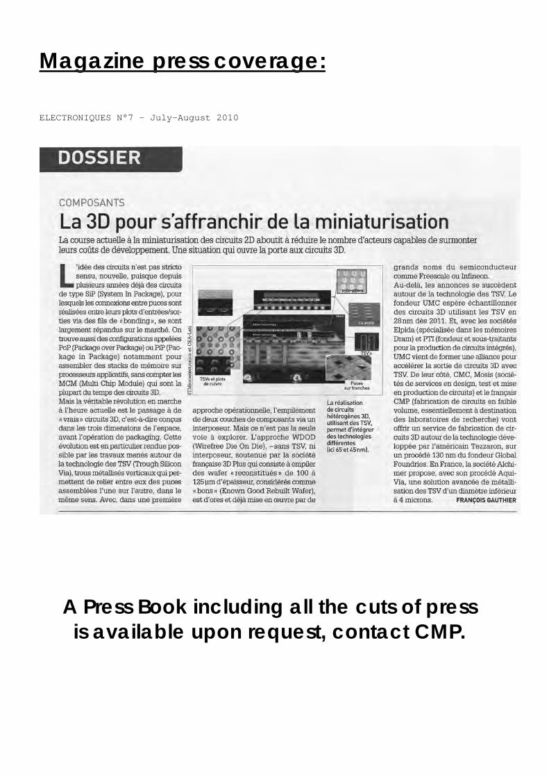
Magazine press coverage: ELECTRONIQUES N°7 – July-August 2010
A Press Book including all the cuts of press is available upon request, contact CMP.

APPENDIX 16: Grenoble’s environment
Grenoble offers a very good environment in terms of Education, Research, High Tech Activities, Industry.
Higher Education Grenoble was awarded the title of "European University and Scientific Pole" in 1990, allowing the universities to stand on the international scene along with Oxford, Bologna or Tubingen. 62 000 students 10 000 foreign students 12,7% higher education 40,2% high school graduates
Research Grenoble is the first French research center in Engineering Sciences, the second in Physics, the third in Mathematics. 1st in France and 5th in Europe for participation by its laboratories in the EU Research and Development Framework Programme.
21 000 researchers (the largest concentration of CNRS researchers in Engineering Sciences after Paris) 1 500 foreign researchers 250 laboratories 11,000 jobs in public research 4,000 jobs in private research 3,500 doctorate students and interns in local laboratories 30% foreigners in doctorate schools
5 European research centers:
ESRF, European Synchrotron Radiation Facility ILL, Laüe Langevin Institute IRAM, Millimetric Radio Astronomy Institute SNCI, National Service for Intense Magnetic Fields EMBL, European Molecular Biology Laboratory
5 National research centers:
CNRS, National Center for Scientific Research Grenoble CEA, Atomic Energy Commission France Telecom R&D CRSSA, Research Centre for the Army Health Services INRIA, National Institute for Research in Computer Science and Control
1 research center of international proportions acquired every 10 years since 1946
High tech Activities Microelectronics : 27% of jobs in France are located in Grenoble Electronics : 470 industrial companies, 16,600 jobs Biomedical technologies : 104 industrial companies, 2,600 jobs Imaging technologies: 50 industrial companies, 800 jobs
1 Technopole as part of Grenoble's regional economic development, the "Zone for Innovation and Scientific and Technological Creation" (ZIRST) has become one of the foremost French technology parks, covering about 280 acres with over 275 companies employing 8500 people, mainly in the sectors of new technologies. MINATEC: joint facility for research in micro and nano technologies.
Industry 3,500 companies created and 1000 buyouts per year in Isère 145 foreign-owned capital companies, employing 28,000 people 1 Business District to welcome company headquarter and professional services (EUROPOLE)

Electronics Education:
Engineering schools of Grenoble INP and UJF ENSE3 ENSIMAG ESISAR GENIE INDUSTRIEL PAGORA PHELMA POLYTECH
Research Laboratories of CNRS, Grenoble INP, UJF
3S-R G-SCOP G2E-Lab GIPSA-lab IMEP-LAHC LEGI LEPMI LGP2 LIG LJK LMGP LPSC LTHE LTM RHEO SIMAP SPINTEC TIMA TIMC VERIMAG
Infrastructures for research and education CIME CMP
Applied research LETI, a division of the French Atomic Energy Commission (CEA) France Telecom R&D, Grenoble Center
Industry STMicroelectronics, ATMEL,Thomson Electronic Tubes, Thomson Consumer Electronics, Thomson
LCD, Schneider Electric, Mentor Graphics, AURIS, Dolphin Integration, SOFRADIR, RADIALL, MEMSCAP, iROC, SOITEC, NanoSprint
A few key dates in local history 43 BC 1st mention of CULARO, a small town modestly built by the Celts to get across the Isère river, by Lucius Munatius Plancus in his correspondence to Ciceron.
339 The town became known as Gratianopolis in honour of the Emperor GRATIEN.
1012 The Saint-Laurent quarter (right bank) is given to the benedictine monks of Saint Chaffre en Velay : founding of the Saint-Laurent priory and then, development of a suburb. 1084 Foundation of the Monastery of the Grande Chartreuse.
1228 Construction of the Collegiate Church Saint André : the "Dauphins" set up their administration in Grenoble.

1339 Creation of a University in Grenoble, including four sections : medicine, liberal arts (sciences and literature), canon law and civic law.
1391 - 1418 Construction of the Island Tower, first Town Hall.
1453 The setting up of the parliament of Grenoble : the town is officially recognised as a regional capital.
1593 - 1606 Construction of the wall of Lesdiguières.
1709 Birth of Jacques DE VAUCANSON, biomechanist. His automata (Le Joueur de Flûte, 1738) were aimed at "reproducing means in view to obtain the experimental intelligence of a biological mechanism".
1712 Birth of Joseph FOURIER, mathematician and prefect of Isère department. In 1811 Joseph FOURIER sets up the Faculty of Sciences. In 1987, the Scientific, Technologic and Medical University of Grenoble will take the name "Université Joseph FOURIER". 1783 Birth of Henri BEYLE, so-called STENDHAL, novelist.
1790 Birth of J.F. CHAMPOLLION, who was the first to decipher Egyptian hieroglyphics in 1824.
1869 Invention of the hydro-electric power, the "White Coal", by Aristide BERGES.

ARISTIDE BERGES PORTRAIT PAINTING BY ALFONS MUCHA, 1902
1907 Start of Rossignol
1920 Start of Merlin Gerin.
1929 ADR is created in Grenoble to help the development of University-Industry cooperation.
1935 First ski-lift manufactured by Pomagalski.
1946 Creation of the National Council for Scientific Research (CNRS).
1950 Thomas WATSON, founder of IBM, is awarded Doctor Honoris Causa on 10 July 1950, the day of the 50th birthday of the Institut Polytechnique de Grenoble (IPG). At this time, Louis BOLLIET is a student at IPG under the supervision of Jean KUNTZMANN. The students are trained on office computers. Two such office computers are depicted below. They can be seen at the ACONIT Museum in Grenoble (Museum of informatics). The third office computer is dating from the same time (donation by Louis COURTOIS to ACONIT).
Mechanical office computer BRUNSVIGA
Electro-mechanical office computer MONROE
Electro-mechanical office computer MONROE

1951 Foundation by J. KUNTZMANN of the Laboratoire de Calcul of IPG.
1960 Creation of ENSIMAG, the IPG school for engineers in informatics and applied mathematics.
1955 Grenoble Atomic Energy Commision (CEA Grenoble).
1963 First laboratory integrated circuit at LETI.
1965 First industrial integrated circuit at SESCOSEM. First computer LAG/INPG-MORS.
1966 Laüe Langevin Institute (ILL).
1968 Creation of the Grenoble IBM Scientific Center twined with the US Cambridge Scientific Center. The Grenoble Center had been visited by T.J. WATSON Junior, Chairman of IBM, son of T.J. WATSON the Founder. Grenoble hosts Winter Olympics.
1970 Louis NEEL is Nobel Prize in Physics. First official services are set up at ADR. Louis NEEL is #0, Louis WEIL is #1, Michel SOUTIF is #2, Jean KUNTZMANN is #5. Louis NEEL has been President of Institut National Polytechnique de Grenoble (formerly Institut Polytechnique de Grenoble), from 1954 to 1976 ; he is now Honorary President of INPG.
1971 Start of Hewlett-Packard. 1973 Start of EFCIS (SGS-Thiomson, STMicroelectronics).
1976 National Centre for Telecommunications Research (CNET).
1985 Nobel Prize awarded to Klaus von KLITZING.
1986 European Synchrotron Radiation Facility (ESRF).
1988 Research Centre for the Army Health Services (CRSSA).
1994 The European Synchrotron Radiation Facility is available to research scientists from virtually all countries.


APPENDIX 17: Protocol issued from the 2-3 October 1986 meeting


APPENDIX 18: Quality Assurance


APPENDIX 19: Examples of ICs and MEMS for BioMed applications
This Appendix is exhibiting examples of ICs and MEMS designed for BioMed applications. These ICs and MEMS are designed on processes available from CMP. BioMed applications of electronics and MEMS in general range from implant devices to biosensors, DNA-based systems analytical protein arrays and cell based systems [1]. Two basic technological prerequisites are micro-fluidic platforms and separation based tools on chips. The goal of this section is not to present an exhaustive panorama of all kinds of BioMed applications that can be reached with some types of electronics and MEMS, but only to address a few examples of what can be achieved with standard processes, available for example from CMP. The users do not need to call for specific custom process developments, they only need to design, they do not need to care about the manufacturing. A. CMOS for Neurosciences CMOS ICs can be used for interfacing with cells and biological objects. Both ICs and neurons (and more generally electroactive cells) work electrically. Electrons and holes in semiconductors and ions in cells are the information carriers. Neurons transmit information along nerves through the action potential that is the depolarisation of their membrane. Due to differences in ion concentration between sides of the cell membrane, neurons present a negative potential inside the membrane. When membrane proteins open ions channels, a depolarisation occurs and propagates along the nerve, it is the propagation of the action potential. By placing a metallic or insulator/semiconductor structure in the vicinity of a neuron membrane, it is possible to measure the depolarisation and thus to access the electrical activity of cells. The idea of trying to build an electrical connection between a living cell and an electronic circuit has started in the 70’s. This idea is based on the measurement of the extracellular potential instead of the intracellular potential thus being a non-invasive method for accessing the electrical activity of cells. Micro Electrode Arrays (MEAs) have then been developed and succeeded in not only measuring the electrical activity of neurons and tissues (the spikes) but also to interfere and initiate action potentials in neurons. Needle shaped microelectrodes have also been developed in order to be implanted in vivo in cerebral tissue and then to record its electrical activity. Despite these remarkable results, MEAs were suffering form limitations in terms of signal / noise ratio and integration possibilities. In 1991, Peter Fromherz [2] has been working on silicon/neuron junction and then developed the first real connection between a neuron and an integrated circuit. These works have been pursued toward a greater integration and soon a real communication between an IC and a neuron [3-4] has been shown. By communication we mean initiation of an action potential in a neuron, propagation to other neurons and then reading of the signals in these other neurons through other microelectrodes in the IC. The integration of real neuron networks with integrated circuits is a very promising technique for neuroscience. However some specific care must be taken for the coupling. For biocompatibility reasons, it is not possible to directly connect a culture medium to the surface of an integrated circuit. The aluminum as an example of metal present in ICs connection pads is not compatible with neurons. Several techniques have been develop to overcome this problem including the use of capacitive electrodes (silicon dioxyde is biocompatible) or the covering of metal electrodes with noble metals such as Platinum. It is shown as an example in the fig. 1 where a square platinum plate covers the top metal opening.

Fig. 1: SEM picture of the grid electrode of an ISFET covered with a platinum layer. This electrode is a part
of an ISFET sensor matrix implemented on CMOS. Apart from an electrical interface with electrically active cells, ICs have been used in several other bio applications such as the measure of ion concentration in the vicinity of cells. This has been done in the purpose to study ionic activity of cells (through membrane proteins) regarding the presence of drugs in the culture medium. In this case, several studies report the use of Ion Sensitive Field Effect Transistors to measure ionic concentration. Another application in cell biology has been to use an IC for localisation and immobilisation of cells. In reference [5], authors have created an array of photodiodes / electrodes included in a microfluidic system. Once a cell is detected through the array of photodetectors it is kept trapped by means of a vertical dielectrophoretic well. This system allows the control of cells population on top of an integrated circuit. All previously described applications have been developed to establish a measure of electrical or ionic activity of living neurons. On another hand, there is an intense research activity on the field of mimicking the behaviour of neurons and synapses in the goal of building artificial analog neuron networks. Neuron networks have been intensively studied and modelled using computers. In the case of neuromorphic ICs [6], a physical implementation of a neuron is made on silicon. It has the advantage of being real time and could be used both for the study of computing techniques and also in the goal of hybridation with a real neuron network. The Fig. 2 is an example of such an analog neuron network, it has been made by researchers in University of Bordeaux [6]. This chip emulates neurons electrical activity using a biophysical model (Hodgkin-Huxley formalism). Five neurons have been integrated and are fully tunable. Their model cards are stored in an analog memory cell array. Such ASICs, as shown in Fig. 2, form the computation core of a complete simulation system dedicated to the investigation of the dynamics of biomimetic neural networks.
Fig. 9: A neuromimetic and modular ASIC: integration of biomimetic neurons
B. Bulk Micromachining for BioMed Bulk micromachining allows the fabrication of various types of sensors for BioMed applications. In the following, an acoustic sensor for ORL surgery is briefly described. Acoustic sensor for ORL surgery

This project is under development jointly at the TIMA Laboratory in Grenoble and at the Hopital Nord in Grenoble. In Oto-Rhino-Laryngology (ORL), the middle ear surgery aims at correcting certain types of hearing loss or in treating certain diseases. Among different kinds of techniques, the ossiculoplasty attempts to re-establish a connection between the tympanic membrane and the oval window. This surgery involves ossicular chain reparation or reconstruction with appropriate replacement prosthesis. Three elements of the ossicular chain (stapes, incus, and malleus), the smallest bones of the human body, provide the sound energy transfer between the tympanic membrane and the inner ear. Successful surgery can lead to the correction of hearing loss due to tympanic membrane anomalies or to a discontinuity or fractures of ear bones. There exists a number of different techniques leading to the ossicular chain reconstruction using either biomaterials or various other materials such as titanium, gold or ceramics. In spite of all this progress, the surgical act in the middle ear remains difficult because of a large number of factors influencing its success. Moreover, there is no available means enabling per-operatory monitoring and thus giving necessary feedback to the surgeon. The project is aimed at the development of a micromachined vibration sensor working in the audible frequency range from 1 to 5 kHz is required by ORL surgeons. Such a sensor, used during a surgery, will make easier to a surgeon to take a decision whether the realized ossiculoplasty is providing an optimal transfer of the acoustic signal from the tympanic membrane to the inner ear. The simplified picture showing the human ear main parts as well as the procedure using the vibration sensor is in Fig. 3. A sound source located in front of the patient’s outer ear generates a test signal that propagates through the external ear to the tympanic membrane. The movement of the tympanic membrane is transferred via the ossicular chain to the input of the inner ear represented by the oval window. The vibration sensor put in contact with any part of the ossicular chain will thus provide real-time information about its degree of mobility and about the quality of the propagated sound signal.
Fig. 3: Illustration of the basic parts of the human ear and of the use of the sensor.
The MEMS-based approach to the sensor design is motivated by the small size and low mechanical impedance of the ossicular chain. A micro-machined sensor tip will provide a possibility of the vibration measurement by a physical contact with no side effects to the ear function. A careful design of the sensor is required in order to overcome the ultra-low level of vibrations (see Fig. 11). The curve in Fig. 4 shows middle-ear displacement values generated by the sound pressure level of 80 dB on the tympanic membrane as obtained from the behavioral model of the ear.
f(Hz)10
210
310
40
2
4
6
8
10
12
14
y(nm
)
f(Hz)10
210
310
40
2
4
6
8
10
12
14
y(nm
)

Fig. 4: Middle-ear bones displacements as a result of the behavioral model of the ear (sound level 80dB). Different possible arrangements of the sensor are investigated. The sensor with a contact tip placed perpendicularly to the sensitive element composed of four arms equipped with piezoresistive gauges is shown in Fig. 5.
Fig. 5: Principle of the sensor structure.
The sensitive element of the sensor is made from the silicon-on-insulator (SoI) wafer. This kind of substrate facilitates the fabrication of arms with uniform thickness. The silicon arms are made by the front side micromachining. The whole sensitive structure is suspended on the cavity obtained with the deep reactive ion etch (DRIE) from the back side of the wafer. The contact tip is formed by a glass fiber attached with a central stem obtained after the patterning and the etching of the bulk silicon layer. Attention must be paid to the resulting characteristics of the mechanical structure. Especially, the mechanical impedance at the end of the tip must match that of the middle ear ossicular chain. Too high value of the mechanical impedance may result in affecting the function or even in damaging the structure of the ear; too low impedance value would not ensure the optimal transfer of the tip movement towards the piezoresistive gauges. One of the results of the sensor structure FE modeling is shown in Fig. 6. The zones of maximal stress on the arms as a result of force load at the end of the tip can be identified here.
Fig. 6: Piezoresistive sensor structure FE modeling.
Another important issue consists in piezoresistive gauges optimization. Extremely low displacement values require high signal-to-noise ratio achieved by optimal geometry and placement of the gauges, by proper doping of the silicon layer and by low-noise electronics applied at the front-end. C. MUMPS for BioMed MUMPS allow the manufacturing of devices in view of various BioMed applications. In the following are addressed successively research applications and commercial applications. 1) Research applications The following examples are coming from Canadian Universities. The projects have been collected by CMC. CMC is the Canadian Microelectronics Corporation, a Service similar to CMP, servicing the

Canadian Universities. The first example is coming from the University of Calgary, Electrical & Computer Eng. (Karan Kaler, Martin P. Mintchev, Electronic Mosquito: A Semi-Invasive MEMS for Blood Sampling and Analysis”). The device would extract blood like a mosquito would, electronically analyze the sample and then transmit it to a wireless device to monitor and control the insulin infusion pump so that the glucose balance in the body of a diabetic patient is maintained throughout the day. The Fig. 7 depicts more in detail the device. The following is taken from the designers.
Fig. 7: The e-Mosquito™ cell: device building blocks include microneedle, microactuator, microsensor,
microelectronics, and microbattery [courtesy from the University of Calgary] The very small volume of blood (<1ml) delivered by the sampling process is stored in a miniature blood compartment, where the microsensor converts the blood element of interest (for example, the glucose level) into an electrical signal. This automated and self-calibrated procedure is performed by a microsensor integrated inside the blood compartment. The major building blocks consist of: (1) a microneedle; (2) a microactuator integrated with the microneedle; (3) a microsensor implemented inside a blood-collecting compartment; (4) a microelectronic stage including analog signal conditioning, analog-to-digital converter, controlling electronic circuitry, and digital radio-frequency transceiver; (5) a microbattery providing the energy to operate the MEMS device; (6) an associated packaging to protect the delicate microsystem inside; (7) an adhesive and antiseptic layer placed between the skin surface and the device; and (8) an enclosing band-aid to attach the e-MosquitoTM patch safely onto the skin. An array of single-use and individually actuated e-MosquitoTM cells form the disposable patch and a matrix of 180 e-MosquitoTM cells can provide periodic blood sampling for up to one week, assuming that blood monitoring is required every hour. An other example comes from Dalhousie University, Mechanical Engineering Department. Ted Hubbard et al. developed a microgripper in view of mechanical testing of cells and bacteria, cell manipulation, medical screening. Initial designs were made on MUMPS, they next moved to Micragem, a SOI MEMS technology from Micralyne, that is available from CMC. The following is taken from [7]. An electrothermal microgripper is used. Typical displacements for chevron actuators are in the range of a few micrometres, so mechanical amplifiers are needed to increase the motion. Fig. 8 shows a chevron actuator with a set of two closed-toggle-style amplifiers, one for each jaw of the gripper. A small displacement downward (along the y- axis) at the centre of the chevron actuator (3) draws in the gripper jaws (6) significantly. The amplifiers (5) are mechanically connected to the actuators (3), and therefore current also flows through them. This means that they will also heat up and thermally expand. To take advantage of his current, the amplifiers are designed to act as hot/cold-arm-type thermal actuators, where the thin-finned hot arm of the actuator is on the outside, contributing to the inward, closing motion of the jaws (6).

Fig. 8: Design of an off-chip gripper: (1) breakable tether; (2) bonding pad;
(3) chevron actuator; (4) cavity; (5) amplifiers; (6) jaws [7] The gripper is able to grasp 5 µm spheres. 2) Commercial applications The following examples are coming from MEMSCAP. The products did not come directly from MUMPS, but MUMPS have served as test vehicles to test various components. The first example is a pressure sensor MEMSCAP is manufacturing for CardioMEMS. The wireless pressure sensor is inserted during the minimally invasive repair of abdominal aortic aneurysms (AAA) or thoracic aortic aneurysms (TAA), via a catheter into a patient’s aneurysm sac. The small size, durability, and lack of wires and batteries enable system to last for, and transmit data over, the lifetime of the patient without requiring repeated procedures (Fig. 9).
Fig. 9: Wireless AAA pressure sensor from CARDIOMEMS
The second example is a wireless imaging system made for Given Imaging in view of endoscopy. The tiny camera contained in a capsule captures images of the gastrointestinal tract as it travels through the body and transmits the images to a computer so a physician can view them and make a diagnosis (Fig. 10).
Fig. 10: PillCam Capsule from Given Imaging
D. ASIMPS for BioMed ASIMPS from Carnegie-Mellon University allow the design of BioMed applications. Here is an example: a bone implantable stress sensor. The following is taken from [8]. The clinical management of skeletal trauma and disease relies on radiographic imaging to infer bone quality. However, bone strength does

not necessarily correlate well with image intensity. There is a need for a safe and convenient way to measure bone strength in situ. The goal is to present a new technique to directly measure bone strength in situ at a micro-level scale through a MEMS sensor. The proposed MEMS stress imager comprises an array of piezoresistive sensor “pixels” to detect stress across the interfacial area between the MEMS chip and bone with resolution to 100 Pa, in 1 sec averaging. The sensors are integrated within a textured surface to accommodate sensor integration into bone. From initial research, surface topography with 30-60 µm features was found to be conducive to guiding new cell growth. Finite Element Analysis (FEA) has led to a sensor design for normal and shear stress detection. The Fig. 11 pictures the MEMS device that includes the piezoresistive sensor array, and a coil antenna for RF power and telemetry. The interest for clinicians is that if they had a practical means to directly measure and quantify biomechanical properties of healing or diseased bone in situ, within bone, this capability could provide improved and timely information for treatment management options, including drugs, fixation adjustments, rehabilitation regiments, or pre-emptive surgical intervention. In contrast to the local nature of the validation in single sensor experiments, an array of piezoresistive elements offers the possibility of global data over an entire surface on the order of 1-4 mm2.
Fig. 11: Bone Implantable Stress Sensor [10]
E. A system view: BioMed science and beauty This last section gives a detailed example of a whole system including various kinds of sensors, ASICs for signal processing, data acquisition, expert systems, etc. It is coming from IntuiSkin, a wholly owned subsidiary of the MEMSCAP Group. IntuiSkin is focused on innovative, technology based skin care solutions. These solutions provide an answer to the new and strong consumer demand for technology based cosmetology. They allow to characterize the skin in general, in order to recommend suitable cosmetic treatments. The general concept of IntuiSkin is depicted in Fig. 12 [9]. The various MEMS sensors are grouped into 2 probes measuring many basic parameters of the skin.

Fig. 12: IntuiSkin general concept [9]
The Visio probe uses its sensors to capture with an extreme precision the skin images. The system enables many measurements including wrinkles, sebum, hairiness, dark spots and clogged pores/bacterial infection. The Physio probe contains sensors and extracts in vivo the key characteristics of the skin. This probe measures, among other parameters, the hydration, the trans-epidermal water loss (TEWL), and the skin temperature. The 2 probes and a few examples of the measured parameters are depicted in Fig. 13.
Fig. 13: The probes and examples of measured parameters [9]
Several equipments and products have been derived by IntuiSkin to address various needs. The Skin Evidence is addressing the medical market. It is an answer to the practician needs in cure and detection as well as in specific treatments (peeling, injection, fillers,…) as well as to the clinician in pre and post surgical support. It is expected that the system will be used by skin specialists, dermatologists, dermato-cosmeticians, plastic surgeons in their clinics or in their office. The other market addressed by the general concept of intuiSkin is the beauty market. The IOMA Beauty Diag™ is measuring the 7 main dysfunctions of the skin: hydration and UV damage, fine lines, wrinkles and elasticity, redness, bacterial infection, sebum, dark spots. It is expected that aestheticians will use the equipment to recommend the best treatments. The last exemplified systems are portable systems for consumer use: the Sensicards™. Sensicards enable to optimize the use of cosmetic products, to watch and check the skin evolution, so as to enjoy the sun benefits with no constraints. SensiCards are systems equipped with sensors, micro-electronics, data displays, batteries, communications interface and data analysis and management. They are custom made and integrated in a light and resistant packaging the size of a credit card. The UV-SensiCard is expected to be used for skin protection against the sun. Once the sun protection factor (SPF) of the available sun cream is selected, this card enables to measure and display the intensity of the ambient UV,

and to recommend for each skin type the time to reapplication of this sun cream. Other SensiCards have been developed along the same general concept. F. What is important for the BioMed community? Many kinds of BioMed applications have been addressed in this paper, ranging from neurosciences to surgery aid, to endoscopy, to skin treatment. Many other kinds of applications might be devised in the future. Going further from dermatology for example, hardware devices might be designed in view of the coming market dealing with dermonutrition or nutricosmetics, depending on the way companies are coming from. Danone is offering yoghurts “nourishing the skin from inside”, and L’Oreal is offering with Nestle nutritional food fighting the skin aging:nutraceuticals with cosmetic benefits(the so-called beauty pills). In both cases, the efficiency can be scientifically measured by specific devices. What is important for the BioMed community is that Education and Research should take advantage of these infrastructures, in the same way as Education and Research in microelectronics have taken advantage of these infrastructures in the 80s. At that time, these infrastructures offered the possibility to EE and CS students, teachers, researchers, to focus on the design of complex circuits hence to focus on the applications, because these infrastructures gave them the opportunity not to be burden by the manufacturing processes, nor by the cost of their projects. Today, various CMOS and MEMS processes can allow students, teachers, researchers to focus on BioMed applications. Not all possible applications can be reached by standard processes offered by service organizations like CMP, but these service organizations are continuously expanding their portfolios. CMC from Canada recently introduced, for example, access to a microfluidics platform. In addition to fixtures for custom fluidic microchips, it gains advantage from multiple technologies--photonics, electronics and embedded software, and pushes further the set of BioMed applications targeted by teachers, researchers and students. References [1] “BioMEMS”, Edited by G. URBAN, Springer, 2006. [2] "A Neuron Silicon Jonction : A Retzius Cell of the Leech on an Insulated Gate Field Effect Transistor", P.
Fromherz et al., Science n° 1952, pp. 1290-1293, 1991. [3] "Silicon-Neuron Junction: Capacitive Stimulation of an Individual Neuron on a Silicon Chip", P.
Fromherz, A. Stett, Physical Revue Letter, n° 75, pp. 1670à 1673, 1995. [4] "A 128x128 Bio-sensor array for extracellular recording of neural activity", P. Fromherz et al. International
Solid State Circuits Conference (ISSCC), 2003. [5] “A CMOS Chip for Individual Cell Manipulation and Detection”, N. Manaresi et al. IEEE Journal of Solid-
State Circuits, Vol.38, n°12, 2003. [6] "Neuromimetic ICs with analog cores: an alternative for simulating spiking neural networks ", S. Renaud
et al. in Proceedings of the IEEE 2007 InternationaI Symposium on Circuits And Systems, (ISCAS'07), New-Orleans, USA, 2007, pp. 3355-3358.
[7] “Theoretical and experimental analysis of an off-chip microgripper”, J. Fraser, T. Hubbard, M. Kujath, Can. J. Elect. Comput. Eng., Vol.31, No.2, Spring 2006.
[8] “BioImplantable Bone Stress Sensor”, F. Alfaro et al, Proc. of the Int’ Conf. of IEEE Engineering in Medicine and Biology Society (EMBS), Shanghai, China, Sept. 1-4, 2005.
[9] “Panel on success stories in MEMS-based systems”, J.M Karam, Design, Test, Integration and Packaging of MEMS and MOEMS Conference, Nice, France, 9-11 April 2008.


APPENDIX 20: Electronics for energy management
This section is taken from the paper given as a companion to an invited talk given at International SoC Design Conference (ISOCC), November 22-24 2009, Busan, Korea. Abstract - This paper deals with how ICs and MEMS can address energy issues like the generation, the conversion, the use, the storage, of energy. Energy management is indeed a major issue for the world. Several domains are reviewed like equipment, buildings, lighting, transport, industry. Such a topic complements another important topic addressed for ICs and MEMS themselves, namely the design of low-power devices. A way for future ultra low power devices is also addressed. ICs and MEMS for energy management can be obtained from CMP that is briefly reviewed. Keywords: energy, power, CO2, photovoltaics
I - INTRODUCTION For a long time the IC power issue has been focusing on the design of low-power ICs and MEMS in order to look for the longest possible battery lifetime of mobile devices, like telephones. This is a very useful goal, but the role of ICs and MEMS in energy management is likely to be even more important. This paper has 4 external sources: the IEA to G8 policy recommendations, in terms of total energy, the keynote by R.P. de VRIES at ISSCC 2009 [1], the keynote by Ch. BELADY at ICCD 2008 [2], and course notes by A. SHAKOURI [3]. The recommendation of IEA to G8 is to save 20% of total energy by 2030. This will reduce by 20% per year the global CO2 emissions by 2030.These savings could come from various domains like Buildings, equipment, Lighting, Transport, Industry, for a total of 92 EJ. Examples of savings are given for several domains in the following.
II - ELECTRONIC EQUIPMENT The standby modes and the operational modes can be considered. It is considered that the standby mode is responsible for 5% to 10% of the total home power consumption. Great savings may be achieved. An example of potential savings in the operational mode can be given with TV displays. The figure 1 displays the power as a function of the size of the screen. When 36M decide to move to home cinema, it means that an additional power plant is necessary…. The worst comes from the fact that plasma TV consumes much more than LCD while plasma TV is recommended for very large screens. These power consumption values are much more higher than the power consumption of the old cathodic displays: around 100 W. Huge savings could be obtained here. MEMS are also offering a hope if TMOS could
replace LCD, plasma and OLED devices [1].
Figure 1: TV power vs. screen size
Data centers were responsible for 1.2% of the total consumption in USA in 2005. Here the design of low-power servers is crucial since every W saved in the die translates into $3 to $4 in support cost. This is important when data centers contain 100.000 or 200.000 servers.
III - AUTOMOTIVE Automotive is a major source of oil consumption: 60% of the world oil is consumed in transport, road vehicles are responsible for 80% of the total transport energy consumption. Much has already been done since 35% decrease in oil consumption per car has been achieved over the last 30 years. But more is recommended to come: 50% more reduction by 2030 and 50% more for light-duty vehicles. Of course, electronics has been and will even be more responsible for these savings.
Electric cars will help on oil consumption on the roads, but they need an electrical source …. (if all cars in France would go electrical, this would lead to +25% to +50% electrical consumption…). So the total process may be not very efficient. Presently, the $ value of batteries is about 30% in an electrical car. Various types of hybrid cars can save oil consumption with stop-start, with the use of electrical power for acceleration, with regenerative braking, with electrical transmission…. Many DC-DC converters are needed, DC-AC are needed, etc.
IV - LIGHTING Lighting is responsible for 20% of total electricity produced. The replacement of incandescent lamps by fluorescent or tube lights can save 80% (EU: by 2012).

The move from discrete power components to integrated solutions for the drive electronics will help. Occupancy detection can also help in savings.
V - BUILDINGS Energy is consumed here for the ventilation, heating, air conditioning, lighting. Metering allows the shaving of peaks (hence of the total capacity), by powering off some devices. Many sensors are required. Concrete examples exist like a zero energy building in France (where 1,600 sensors and 550 sqm of PV are used) and a rotating solar building in Germany.
VI - THE DEVELOPMENT OF SOLAR ENERGY Here is another example of the use of electronics. The power output of a PV cell is maximized when the cell is operated at an optimal voltage, depending on the temperature and on the irradiance. This is illustrated by the figures 2, 3 and 4. Electronics is necessary to optimize the power generation. The installed PV capacity is expected to grow by 20% to 40% per annum, and to increase rapidly when the parity cost will be achieved (between 2012 and 2018 depending on the countries).
Figure 2: Optimum Load for Single Photovoltaic Cell (National Semiconductor)
Figure 3: Temperature Dependence of a PV Module (National
Semiconductor)
Figure 4: Irradiance Dependence of a PV Module (National
Semiconductor)
VII - ICS AND MEMS AVAILABLE FROM CMP CMP is a non profit Service, reporting to CNRS (the French National Council for Research) and to Universities in Grenoble. CMP aims to serve Universities, Research Labs and Companies in ICs and MEMS fabrication. CMP give access to a number of technologies, for prototyping and low volume production. Since 1981, CMP has served more than 1,000 institutions from 70 countries in various processes. Support to Industry started in 1990. Development at CMP Several periods may be distinguished. 1981–1982 : launching CMP with NMOS 1983–1984 : development of NMOS, launching CMOS 1984–1986 : development of CMOS 1987–1989 : abandon NMOS, increase the frequency of CMOS runs 1990–1994 : launching Bipolar, BiCMOS, GaAs MESFET, GaAs HEMT, advanced CMOS (.5 µ TLM) 1995–1997 : launching CMOS and GaAs compatible MEMS, DOEs, deep-submicron CMOS (.25µ 6LM) 1998 : launching silicon surface micromachining, abandon MESFET GaAs 1999 : launching SiGe, deep submicron CMOS (.18µ 6LM), SOI/SOS CMOS (.5µ) 2000 : launching SiGe BiCMOS (.35µ 5LM) 2001 : launching very deep submicron CMOS (.12µ 6LM) 2002 : launching Inp HBT process 2003 : launching 0.35µ CMOS-Opto 2004 : launching very deep submicron CMOS (90nm, 7LM), HBT Sige:C BiCMOS 0.25µ 2006 : launching CMOS 65nm (7LM) 2008 : launching CMOS 45nm
Processes available Presently the processes available for ICs manufacturing are depicted in Table 1.
Austriamicrosystems 0.35µ CMOS C35B4C3

0.35µ CMOS C35B4M3 0.35µ CMOS-Opto C35B4O10.35µ CMOS Flash C35B4E3 0.35µ SiGe BiCMOS S35D4M5
0.35µ HV-CMOS H35B4D3 45nm CMOS CMOS045 65nm SOI 65nm CMOS CMOS065 90nm CMOS CMOS090
STMicroelectronics
130nm CMOS HCMOS9GP 130nm SOI 0.25µ SiGe:C BiCMOS7RF OMMIC 0.2µ HEMT GaAs ED02AH
Table 1: IC processes available
ICs design kits and CAD software Design kits and libraries are distributed by CMP for most of the processes and most commonly used CAD tools. CMP sometimes develop design kits, in cooperation with the manufacturers and the CAD vendors. CMP also offers special CAD software conditions from a few CAD vendors. As a focal point, CMP also distributes information on configuration files, converters, etc. About 40 design kits are available for each process and the main CAD tools. Test and packaging Packaging and testing services are also offered. Various types of packages are supported, including DIL, SOIC, CQFP, JLCC, PGA, etc. Test of prototypes is usually done by the final user. On request, especially for low volume production, CMP may take over testing together with manufacturing. MEMS CMP offers several processes for MEMS manufacturing based on bulk micromachining, as well as specific MEMS processes. These are depicted in Table 2.
Base Austriamicrosystems .35µ Base STMicroelectronics .25µ BiCMOS
Integrated micromachining
post-process ASIMPS from CMU PolyMUMPS from MEMSCAP MetalMUMPS from MEMSCAP SOIMUMPS from MEMSCAP
Specific MEMS
SUMMiT V from SANDIA
Table 2: MEMS processes available
VIII - CONCLUSIONS Energy management is a formidable challenge to the world. Electronics will greatly help in coping with that challenge. CMP can help by providing an infrastructure
for Students, Researchers, SMEs to prototype and obtain small volume production. Other than energy management key application areas are healthcare, environment and security. CMP provided a help in many BioMed applications [4]. To cope with all these challenges, CMP will develop along several lines. A. More Moore It has been recognized that Students, Researchers and SME designers must be provided with the possibility to have their circuits fabricated. From its inception in 1981, CMP has been successfully pursuing this goal and experiencing a very significant growth to reach and to keep its present level. The success is partly due to the basic principles which have been governing the choices of the Service: use of industrial and advanced process lines. Advanced processes are more and more necessary because of the need for very skilled designers and because CAD industrial software is more widely available to Universities (instead of University CAD software). Since new versions of CAD software are targeted to industrial use, there is no choice but to use advanced processes. Industry makes also more and more use of the Service. During the 80s, the CMP processes were not very advanced, but they approached more and more industry state of the art during the 90s, because of CAD software reasons and because of the increasing industry use of CMP. Since then, CMP is always offering state of the art processes. CMP introduced 130nm CMOS as early as 2001. A total of 250 circuits were fabricated. CMP introduced 90nm CMOS in 2004 and 242 circuits have been fabricated up to now. 65nm CMOS was launched in 2006 and 57 circuits have been fabricated so far. This means a total of more than 500 circuits coming from about 50 Research Laboratories and Industrial Companies. These processes have been very well received. CMP next introduced 45nm CMOS in 2008. First runs are scheduled in 2009. CMP will proceed with further downsized processes. But it should be clear that the downsizing will…. go down, to get to an end for several reasons, like cost, acceptance, power density, temperature, variability, leakage power, lengthening of money-making time for a generation. And fundamental limits will be reached coming from thermodynamics, quantum mechanisms, electromagnetics, etc. B.- More than Moore But the never ending quest for more complex systems may be satisfied by other technology developments, like the move to 3D processes, possibly not including very advanced process dies. 3D processes lead to easier to manage interconnections and to reasonable cost. CMP will introduce soon 3D processes using TSVs (through silicon vias). It is also recognized that complementary developments

must be addressed, in order to address more diversified needs. With this respect, CMP has been a pioneer in being the first service in the world to offer MEMS processes as early as 1995. Going further, more than mechanics-electronics is to be addressed like photonics, optics, fluidics, etc. CMP will be actively promoting these developments in the future.
REFERENCES [1] Leaner and Greener: Adapting to a Changing Climate of
Innovation, R.P. de VRIES, International Solid-State Circuits Conference (ISSCC), San Francisco, 8-12 February 2009
[2] Lean IT: Lead or Die, Ch. BELADY, keynote at International Conference on Computer Design (ICCD), Lake Tahoe, 12-15 October 2008
[3] A. SHAKOURI, course notes, University of California Santa Cruz [4] Infrastructures for Education, Research and Industry: CMOS and
MEMS for BioMed B. COURTOIS, B. CHARLOT*, G. DI PENDINA, L. RUFER** Invited paper at the 12th World Multi-Conference or Systemics,
Cybernetics and Informatics (WMSCI 2008), Orlando USA, 29 June – 2 July 2008
*IES/MITEA, Montpellier - France,

APPENDIX 21: Contact persons
- CMP STAFF -
Virginie ABBINANTE
Shipments Phone: +33 4 76 57 49 46
Isabelle AMIELH
Executive Secretariat, finance Phone: +33 4 76 57 46 17
Chantal BÉNIS-MOREL Conference Management Phone: +33 4 76 57 46 22
Patricia CHASSAT Secretariat Phone: +33 4 76 57 47 47
Bernard COURTOIS
Director Phone: +33 4 76 57 46 17
Julien DÉSAILLOUD
Administrator of systems and networks, Webmaster Phone: +33 4 76 57 49 87
Grégory DI PENDINA
Data preparation ICs, Micromachining (MEMS), PV Foundries: austriamicrosystems, MEMSCAP Phone: +33 4 76 57 46 21
Sophie DUMONT CAD & Design-kit Technical support Foundries: STMicroelectronics: 65 nm
Phone: +33 4 76 57 48 34
Sylvaine EYRAUD I/O data management of the manufacturing runs
Phone: +33 4 76 57 47 97

Azedine MANAA
Data preparation ICs (with G. DI PENDINA) Phone: +33 4 76 57 46 21
Clothilde NEBON Data preparation ICs (with S. DUMONT) Phone: +33 4 76 57 46 19
Jean-François PAILLOTIN
Foundries: STMicroelectronics: 130 nm Phone: +33 4 76 57 47 97
Joëlle PARRAU Accountant
Phone: +33 4 76 57 46 14
Kholdoun TORKI Technical Director
Phone: +33 4 76 57 47 63
Romain VERLY Support of ARM and Tanner CAD tools
Phone: +33 4 76 57 48 65
- CMP INFORMATION -
CMP 46, avenue Félix Viallet 38031 GRENOBLE Cedex FRANCE
E-Mail [email protected]
PHONE +33 4 76 57 46 17
FAX +33 4 76 47 38 14 +33 4 76 50 95 33
wwwwww http://cmp.imag.fr


Fig. 1: SEM picture of the grid electrode of an ISFET covered with a platinum layer. This electrode is a part
of an ISFET sensor matrix implemented on CMOS. Apart from an electrical interface with electrically active cells, ICs have been used in several other bio applications such as the measure of ion concentration in the vicinity of cells. This has been done in the purpose to study ionic activity of cells (through membrane proteins) regarding the presence of drugs in the culture medium. In this case, several studies report the use of Ion Sensitive Field Effect Transistors to measure ionic concentration. Another application in cell biology has been to use an IC for localisation and immobilisation of cells. In reference [5], authors have created an array of photodiodes / electrodes included in a microfluidic system. Once a cell is detected through the array of photodetectors it is kept trapped by means of a vertical dielectrophoretic well. This system allows the control of cells population on top of an integrated circuit. All previously described applications have been developed to establish a measure of electrical or ionic activity of living neurons. On another hand, there is an intense research activity on the field of mimicking the behaviour of neurons and synapses in the goal of building artificial analog neuron networks. Neuron networks have been intensively studied and modelled using computers. In the case of neuromorphic ICs [6], a physical implementation of a neuron is made on silicon. It has the advantage of being real time and could be used both for the study of computing techniques and also in the goal of hybridation with a real neuron network. The Fig. 2 is an example of such an analog neuron network, it has been made by researchers in University of Bordeaux [6]. This chip emulates neurons electrical activity using a biophysical model (Hodgkin-Huxley formalism). Five neurons have been integrated and are fully tunable. Their model cards are stored in an analog memory cell array. Such ASICs, as shown in Fig. 2, form the computation core of a complete simulation system dedicated to the investigation of the dynamics of biomimetic neural networks.
Fig. 9: A neuromimetic and modular ASIC: integration of biomimetic neurons
B. Bulk Micromachining for BioMed Bulk micromachining allows the fabrication of various types of sensors for BioMed applications. In the following, an acoustic sensor for ORL surgery is briefly described. Acoustic sensor for ORL surgery

This project is under development jointly at the TIMA Laboratory in Grenoble and at the Hopital Nord in Grenoble. In Oto-Rhino-Laryngology (ORL), the middle ear surgery aims at correcting certain types of hearing loss or in treating certain diseases. Among different kinds of techniques, the ossiculoplasty attempts to re-establish a connection between the tympanic membrane and the oval window. This surgery involves ossicular chain reparation or reconstruction with appropriate replacement prosthesis. Three elements of the ossicular chain (stapes, incus, and malleus), the smallest bones of the human body, provide the sound energy transfer between the tympanic membrane and the inner ear. Successful surgery can lead to the correction of hearing loss due to tympanic membrane anomalies or to a discontinuity or fractures of ear bones. There exists a number of different techniques leading to the ossicular chain reconstruction using either biomaterials or various other materials such as titanium, gold or ceramics. In spite of all this progress, the surgical act in the middle ear remains difficult because of a large number of factors influencing its success. Moreover, there is no available means enabling per-operatory monitoring and thus giving necessary feedback to the surgeon. The project is aimed at the development of a micromachined vibration sensor working in the audible frequency range from 1 to 5 kHz is required by ORL surgeons. Such a sensor, used during a surgery, will make easier to a surgeon to take a decision whether the realized ossiculoplasty is providing an optimal transfer of the acoustic signal from the tympanic membrane to the inner ear. The simplified picture showing the human ear main parts as well as the procedure using the vibration sensor is in Fig. 3. A sound source located in front of the patient’s outer ear generates a test signal that propagates through the external ear to the tympanic membrane. The movement of the tympanic membrane is transferred via the ossicular chain to the input of the inner ear represented by the oval window. The vibration sensor put in contact with any part of the ossicular chain will thus provide real-time information about its degree of mobility and about the quality of the propagated sound signal.
Fig. 3: Illustration of the basic parts of the human ear and of the use of the sensor.
The MEMS-based approach to the sensor design is motivated by the small size and low mechanical impedance of the ossicular chain. A micro-machined sensor tip will provide a possibility of the vibration measurement by a physical contact with no side effects to the ear function. A careful design of the sensor is required in order to overcome the ultra-low level of vibrations (see Fig. 11). The curve in Fig. 4 shows middle-ear displacement values generated by the sound pressure level of 80 dB on the tympanic membrane as obtained from the behavioral model of the ear.
f(Hz)10
210
310
40
2
4
6
8
10
12
14
y(nm
)
f(Hz)10
210
310
40
2
4
6
8
10
12
14
y(nm
)

Fig. 4: Middle-ear bones displacements as a result of the behavioral model of the ear (sound level 80dB). Different possible arrangements of the sensor are investigated. The sensor with a contact tip placed perpendicularly to the sensitive element composed of four arms equipped with piezoresistive gauges is shown in Fig. 5.
Fig. 5: Principle of the sensor structure.
The sensitive element of the sensor is made from the silicon-on-insulator (SoI) wafer. This kind of substrate facilitates the fabrication of arms with uniform thickness. The silicon arms are made by the front side micromachining. The whole sensitive structure is suspended on the cavity obtained with the deep reactive ion etch (DRIE) from the back side of the wafer. The contact tip is formed by a glass fiber attached with a central stem obtained after the patterning and the etching of the bulk silicon layer. Attention must be paid to the resulting characteristics of the mechanical structure. Especially, the mechanical impedance at the end of the tip must match that of the middle ear ossicular chain. Too high value of the mechanical impedance may result in affecting the function or even in damaging the structure of the ear; too low impedance value would not ensure the optimal transfer of the tip movement towards the piezoresistive gauges. One of the results of the sensor structure FE modeling is shown in Fig. 6. The zones of maximal stress on the arms as a result of force load at the end of the tip can be identified here.
Fig. 6: Piezoresistive sensor structure FE modeling.
Another important issue consists in piezoresistive gauges optimization. Extremely low displacement values require high signal-to-noise ratio achieved by optimal geometry and placement of the gauges, by proper doping of the silicon layer and by low-noise electronics applied at the front-end. C. MUMPS for BioMed MUMPS allow the manufacturing of devices in view of various BioMed applications. In the following are addressed successively research applications and commercial applications. 1) Research applications The following examples are coming from Canadian Universities. The projects have been collected by CMC. CMC is the Canadian Microelectronics Corporation, a Service similar to CMP, servicing the

Canadian Universities. The first example is coming from the University of Calgary, Electrical & Computer Eng. (Karan Kaler, Martin P. Mintchev, Electronic Mosquito: A Semi-Invasive MEMS for Blood Sampling and Analysis”). The device would extract blood like a mosquito would, electronically analyze the sample and then transmit it to a wireless device to monitor and control the insulin infusion pump so that the glucose balance in the body of a diabetic patient is maintained throughout the day. The Fig. 7 depicts more in detail the device. The following is taken from the designers.
Fig. 7: The e-Mosquito™ cell: device building blocks include microneedle, microactuator, microsensor,
microelectronics, and microbattery [courtesy from the University of Calgary] The very small volume of blood (<1ml) delivered by the sampling process is stored in a miniature blood compartment, where the microsensor converts the blood element of interest (for example, the glucose level) into an electrical signal. This automated and self-calibrated procedure is performed by a microsensor integrated inside the blood compartment. The major building blocks consist of: (1) a microneedle; (2) a microactuator integrated with the microneedle; (3) a microsensor implemented inside a blood-collecting compartment; (4) a microelectronic stage including analog signal conditioning, analog-to-digital converter, controlling electronic circuitry, and digital radio-frequency transceiver; (5) a microbattery providing the energy to operate the MEMS device; (6) an associated packaging to protect the delicate microsystem inside; (7) an adhesive and antiseptic layer placed between the skin surface and the device; and (8) an enclosing band-aid to attach the e-MosquitoTM patch safely onto the skin. An array of single-use and individually actuated e-MosquitoTM cells form the disposable patch and a matrix of 180 e-MosquitoTM cells can provide periodic blood sampling for up to one week, assuming that blood monitoring is required every hour. An other example comes from Dalhousie University, Mechanical Engineering Department. Ted Hubbard et al. developed a microgripper in view of mechanical testing of cells and bacteria, cell manipulation, medical screening. Initial designs were made on MUMPS, they next moved to Micragem, a SOI MEMS technology from Micralyne, that is available from CMC. The following is taken from [7]. An electrothermal microgripper is used. Typical displacements for chevron actuators are in the range of a few micrometres, so mechanical amplifiers are needed to increase the motion. Fig. 8 shows a chevron actuator with a set of two closed-toggle-style amplifiers, one for each jaw of the gripper. A small displacement downward (along the y- axis) at the centre of the chevron actuator (3) draws in the gripper jaws (6) significantly. The amplifiers (5) are mechanically connected to the actuators (3), and therefore current also flows through them. This means that they will also heat up and thermally expand. To take advantage of his current, the amplifiers are designed to act as hot/cold-arm-type thermal actuators, where the thin-finned hot arm of the actuator is on the outside, contributing to the inward, closing motion of the jaws (6).

Fig. 8: Design of an off-chip gripper: (1) breakable tether; (2) bonding pad;
(3) chevron actuator; (4) cavity; (5) amplifiers; (6) jaws [7] The gripper is able to grasp 5 µm spheres. 2) Commercial applications The following examples are coming from MEMSCAP. The products did not come directly from MUMPS, but MUMPS have served as test vehicles to test various components. The first example is a pressure sensor MEMSCAP is manufacturing for CardioMEMS. The wireless pressure sensor is inserted during the minimally invasive repair of abdominal aortic aneurysms (AAA) or thoracic aortic aneurysms (TAA), via a catheter into a patient’s aneurysm sac. The small size, durability, and lack of wires and batteries enable system to last for, and transmit data over, the lifetime of the patient without requiring repeated procedures (Fig. 9).
Fig. 9: Wireless AAA pressure sensor from CARDIOMEMS
The second example is a wireless imaging system made for Given Imaging in view of endoscopy. The tiny camera contained in a capsule captures images of the gastrointestinal tract as it travels through the body and transmits the images to a computer so a physician can view them and make a diagnosis (Fig. 10).
Fig. 10: PillCam Capsule from Given Imaging
D. ASIMPS for BioMed ASIMPS from Carnegie-Mellon University allow the design of BioMed applications. Here is an example: a bone implantable stress sensor. The following is taken from [8]. The clinical management of skeletal trauma and disease relies on radiographic imaging to infer bone quality. However, bone strength does

not necessarily correlate well with image intensity. There is a need for a safe and convenient way to measure bone strength in situ. The goal is to present a new technique to directly measure bone strength in situ at a micro-level scale through a MEMS sensor. The proposed MEMS stress imager comprises an array of piezoresistive sensor “pixels” to detect stress across the interfacial area between the MEMS chip and bone with resolution to 100 Pa, in 1 sec averaging. The sensors are integrated within a textured surface to accommodate sensor integration into bone. From initial research, surface topography with 30-60 µm features was found to be conducive to guiding new cell growth. Finite Element Analysis (FEA) has led to a sensor design for normal and shear stress detection. The Fig. 11 pictures the MEMS device that includes the piezoresistive sensor array, and a coil antenna for RF power and telemetry. The interest for clinicians is that if they had a practical means to directly measure and quantify biomechanical properties of healing or diseased bone in situ, within bone, this capability could provide improved and timely information for treatment management options, including drugs, fixation adjustments, rehabilitation regiments, or pre-emptive surgical intervention. In contrast to the local nature of the validation in single sensor experiments, an array of piezoresistive elements offers the possibility of global data over an entire surface on the order of 1-4 mm2.
Fig. 11: Bone Implantable Stress Sensor [10]
E. A system view: BioMed science and beauty This last section gives a detailed example of a whole system including various kinds of sensors, ASICs for signal processing, data acquisition, expert systems, etc. It is coming from IntuiSkin, a wholly owned subsidiary of the MEMSCAP Group. IntuiSkin is focused on innovative, technology based skin care solutions. These solutions provide an answer to the new and strong consumer demand for technology based cosmetology. They allow to characterize the skin in general, in order to recommend suitable cosmetic treatments. The general concept of IntuiSkin is depicted in Fig. 12 [9]. The various MEMS sensors are grouped into 2 probes measuring many basic parameters of the skin.

Fig. 12: IntuiSkin general concept [9]
The Visio probe uses its sensors to capture with an extreme precision the skin images. The system enables many measurements including wrinkles, sebum, hairiness, dark spots and clogged pores/bacterial infection. The Physio probe contains sensors and extracts in vivo the key characteristics of the skin. This probe measures, among other parameters, the hydration, the trans-epidermal water loss (TEWL), and the skin temperature. The 2 probes and a few examples of the measured parameters are depicted in Fig. 13.
Fig. 13: The probes and examples of measured parameters [9]
Several equipments and products have been derived by IntuiSkin to address various needs. The Skin Evidence is addressing the medical market. It is an answer to the practician needs in cure and detection as well as in specific treatments (peeling, injection, fillers,…) as well as to the clinician in pre and post surgical support. It is expected that the system will be used by skin specialists, dermatologists, dermato-cosmeticians, plastic surgeons in their clinics or in their office. The other market addressed by the general concept of intuiSkin is the beauty market. The IOMA Beauty Diag™ is measuring the 7 main dysfunctions of the skin: hydration and UV damage, fine lines, wrinkles and elasticity, redness, bacterial infection, sebum, dark spots. It is expected that aestheticians will use the equipment to recommend the best treatments. The last exemplified systems are portable systems for consumer use: the Sensicards™. Sensicards enable to optimize the use of cosmetic products, to watch and check the skin evolution, so as to enjoy the sun benefits with no constraints. SensiCards are systems equipped with sensors, micro-electronics, data displays, batteries, communications interface and data analysis and management. They are custom made and integrated in a light and resistant packaging the size of a credit card. The UV-SensiCard is expected to be used for skin protection against the sun. Once the sun protection factor (SPF) of the available sun cream is selected, this card enables to measure and display the intensity of the ambient UV,

and to recommend for each skin type the time to reapplication of this sun cream. Other SensiCards have been developed along the same general concept. F. What is important for the BioMed community? Many kinds of BioMed applications have been addressed in this paper, ranging from neurosciences to surgery aid, to endoscopy, to skin treatment. Many other kinds of applications might be devised in the future. Going further from dermatology for example, hardware devices might be designed in view of the coming market dealing with dermonutrition or nutricosmetics, depending on the way companies are coming from. Danone is offering yoghurts “nourishing the skin from inside”, and L’Oreal is offering with Nestle nutritional food fighting the skin aging:nutraceuticals with cosmetic benefits(the so-called beauty pills). In both cases, the efficiency can be scientifically measured by specific devices. What is important for the BioMed community is that Education and Research should take advantage of these infrastructures, in the same way as Education and Research in microelectronics have taken advantage of these infrastructures in the 80s. At that time, these infrastructures offered the possibility to EE and CS students, teachers, researchers, to focus on the design of complex circuits hence to focus on the applications, because these infrastructures gave them the opportunity not to be burden by the manufacturing processes, nor by the cost of their projects. Today, various CMOS and MEMS processes can allow students, teachers, researchers to focus on BioMed applications. Not all possible applications can be reached by standard processes offered by service organizations like CMP, but these service organizations are continuously expanding their portfolios. CMC from Canada recently introduced, for example, access to a microfluidics platform. In addition to fixtures for custom fluidic microchips, it gains advantage from multiple technologies--photonics, electronics and embedded software, and pushes further the set of BioMed applications targeted by teachers, researchers and students. References [1] “BioMEMS”, Edited by G. URBAN, Springer, 2006. [2] "A Neuron Silicon Jonction : A Retzius Cell of the Leech on an Insulated Gate Field Effect Transistor", P.
Fromherz et al., Science n° 1952, pp. 1290-1293, 1991. [3] "Silicon-Neuron Junction: Capacitive Stimulation of an Individual Neuron on a Silicon Chip", P.
Fromherz, A. Stett, Physical Revue Letter, n° 75, pp. 1670à 1673, 1995. [4] "A 128x128 Bio-sensor array for extracellular recording of neural activity", P. Fromherz et al. International
Solid State Circuits Conference (ISSCC), 2003. [5] “A CMOS Chip for Individual Cell Manipulation and Detection”, N. Manaresi et al. IEEE Journal of Solid-
State Circuits, Vol.38, n°12, 2003. [6] "Neuromimetic ICs with analog cores: an alternative for simulating spiking neural networks ", S. Renaud
et al. in Proceedings of the IEEE 2007 InternationaI Symposium on Circuits And Systems, (ISCAS'07), New-Orleans, USA, 2007, pp. 3355-3358.
[7] “Theoretical and experimental analysis of an off-chip microgripper”, J. Fraser, T. Hubbard, M. Kujath, Can. J. Elect. Comput. Eng., Vol.31, No.2, Spring 2006.
[8] “BioImplantable Bone Stress Sensor”, F. Alfaro et al, Proc. of the Int’ Conf. of IEEE Engineering in Medicine and Biology Society (EMBS), Shanghai, China, Sept. 1-4, 2005.
[9] “Panel on success stories in MEMS-based systems”, J.M Karam, Design, Test, Integration and Packaging of MEMS and MOEMS Conference, Nice, France, 9-11 April 2008.