Embed Size (px)
Citation preview

CMOS Reliability Characterization Techniques and
Spintronics-Based Mixed-Signal Circuits
A DISSERTATION
SUBMITTED TO THE FACULTY OF THE GRADUATE SCHOOL
OF THE UNIVERSITY OF MINNESOTA
BY
Won Ho Choi
IN PARTIAL FULFILLMENT OF THE REQUIREMENTS
FOR THE DEGREE OF
DOCTOR OF PHILOSOPHY
Chris H. Kim, Advisor
September 2015

© Won Ho Choi 2015

i
Acknowledgements
First of all, I would like to express my deepest gratitude to my advisor, Prof. Chris
H. Kim. As a PhD student, it was my great honor to meet Prof. Kim as a research
adviser and work with him. I am so grateful to Prof. Kim for his endless patience,
encouragement and support for the last four years. I learned a lot from him including
all the technical things such as circuit designs, how to build solid ideas, how to write
good papers, how to present the ideas intuitively and so on. In addition to all these
things, he also has taught me how to lead the research project, especially collaboration
project, in both technical and ethical way. Prof. Kim, I really appreciate your advice
and constant support for the past four years.
Next, I would like to thank the members of my final defense committee:
Professors Sachin Sapatnekar, Jian-Ping Wang, Hubert H. Lim. I appreciate you
taking time out of your busy schedules to critique my work. I am also grateful to
Professors Ramesh Harjani and Kia Bazargan for serving on my preliminary oral
defense committee.
I also have learned and experienced many practical mixed-signal circuit researches
from the summer internships at Intel, Broadcom, Qualcomm, and IBM T.J. Watson. I
must really thank many mentors and managers throughout my internships, Mahesh
Chheda from Intel, Roy Carlson from Broadcom, Dr. Baiying Yu from Qualcomm,
and Dr. Pong-Fei Lu from IBM T.J. Watson. I really appreciate for all the helps,
feedbacks, supports while doing the internships. I also would like to thank all other
colleagues that I have met and spent time together during the internships.

ii
I won’t forget all the good memories that I have with all my colleagues that I met
in the VLSI research group at Minnesota. Firstly, I especially have to thank Jongyeon
Kim, Dr. Hoonki Kim, Xiaofei Wang, Saroj Satapathy, Qianying Tang, and Yang Lv
(Prof. Wang’s group) for their devotional collaborations with me. I also would like to
thank Bongjin Kim for his advice on the tape-out projects. All nights we spent
together for the tape-outs are unforgettable. I thank all my senior group members, Ki
Chul Chun, Wei Zhang, Pulkit Jain, Xiaofei Wang, Seung-hwan Song and Ayan Paul
for all the helps and supports. Also, I thank Weichao Xu, Somnath Kundu, Chen Zhou,
Paul Mazanec, Saurabh Kumar, Ibrahim Ahmed, Muqing Liu, Seokkyun Ko, Deepak
Kumar Tagare, Abhishek Deshpande, Dan Liu, Woong Choi, and Gyuseong Kang.
I would like to thank all my friends living in Minnesota especially, Daehan Yoo,
Jongyeon Kim, Albert Wooju Jang, and Sechul Park. I wish all the best luck for them.
I want to also thank Professors Soo-Won Kim, Chulwoo Kim, Jongsun Park at
Korea University, Korea for their all the supports. Also, I would like to thank Dr. Joo-
Sun Choi, Dr, Jung-Hwan Choi, Dr. Indal Song, Kyungtae Kang, Sanghee Kim, Yong
Shim, Taesik Na, Haeyoung Chung, and all other colleagues who were in DRAM
design team at Samsung Electronics in Korea.
I dedicate my thesis to my parents and parents in law. Words fall short in
describing what they have done for me. Also, I would like to express my deepest love
and appreciation to my wife, Ji Young Park. Your patience with me is astounding, and
a great lesson that I will continue to learn from for many years. I love you and thank
you for everything. Finally, I truly love you forever, my son, Eric Yejun Choi.

iii
Abstract
Plasma-Induced Damage (PID) has been an important reliability concern for
equipment vendors and fabs in both traditional SiO2 based and advanced high-k
dielectric based processes. Plasma etching and ashing are extensively used in a typical
CMOS back-end process. During the plasma steps, the metal interconnect, commonly
referred to as an “antenna,” collects plasma charges and if the junction of the driver is
too small to quickly discharge the node voltage, extra traps are generated in the gate
dielectric of the receiver thereby worsening device reliability mechanisms such as Bias
Temperature Instability (BTI) and Time Dependent Dielectric Breakdown (TDDB).
The foremost challenge to an effective PID mitigation strategy is in the collection of
massive TDDB or NBTI data within a short test time. In Chapter 2, we have
developed two array-based on-chip monitoring circuits for characterizing latent PID
including (1) an array-based PID-induced TDDB characterization circuit and (2) a
PID-induced BTI characterization circuit using the 65nm CMOS process.
As the research interest on analog circuit reliability is increasing recently, a few
studies analyzed the impact of short-term Vth shift, not a permanent Vth shift, on a
Successive Approximation Register (SAR) Analog-to-Digital Converter (ADC) and
revealed that even short-term Vth shifts in the order of 1mV by short stress pulse (e.g.,
1μs) on the comparator input transistors may cause to degrade the resolution of the
SAR ADC even for a fresh chip (no experimentally verified). In Chapter 3, we
quantified this effect through test-chip studies and propose two simple circuit
approaches that can be used to mitigate short-term Vth instability issues in SAR ADCs.

iv
The proposed techniques were implemented in 10-bit SAR ADC using the 65nm
CMOS process.
Spintronic circuits and systems have several unique properties including inherent
non-volatility that can be uniquely exploited for achievable functional capabilities not
obtainable in conventional systems. Magnetic Tunnel Junction (MTJ) technology has
matured to the point where commercial spin transfer torque MRAM (STT-MRAM)
chips are currently being developed. This work aims at leveraging and complimenting
on-going development efforts in MTJ technology for non-memory mixed-signal
applications. In Chapter 4, we developed three spintronics-based mixed-signal circuit
designs: (1) an MTJ-based True Random Number Generator (TRNG), (2) an MTJ-
based ADC, and (3) an MTJ-based temperature sensor. The proposed TRNG, ADC,
and temperature sensor have the potential to achieve a compact area, simpler design,
and reliable operation as compared to their CMOS counterparts.
STT-MRAM is one of the promising candidates as a scalable nonvolatile memory
with high density, and CMOS compatibility. Interface Perpendicular Magnetic Tunnel
Junction (I-PMTJ) has been demonstrated with the goal of reducing the switching
current while maintaining sufficient nonvolatility. However, previous studies report
that I-PMTJ suffers from process-dependent dimensional variations, thus it remains
one of the major constrains in achieving high performance STT-MRAM. In Chapter 5,
we present a comprehensive study on process-dependent dimensional variability of
PMTJ, especially focusing on estimating the impact of the free layer thickness (tF)
variation on thermal stability factor (Δ) and switching current (IC) variability.

v
Content
List of Figures .............................................................................................................. viii
Chapter 1 Introduction ................................................................................................ 1
1.1 Latent Plasma-Induced Damage (PID) ................................................................ 2
1.2 Reliability Issues in Successive Approximation Register (SAR) ADC .............. 3
1.3 Magnetic Tunnel Junction (MTJ) ........................................................................ 4
1.4 Summary of Thesis Contributions ....................................................................... 7
Chapter 2 On-chip Monitoring Circuits for Characterizing Latent PID .............. 10
2.1 Introduction ....................................................................................................... 10
2.2 Prior Work on PID Characterization ................................................................. 14
2.3 Proposed PID-induced TDDB Characterization Circuit Design ....................... 19
2.3.1 Test DUT Array Design .......................................................................... 19
2.3.2 On-chip Current-to-Digital Converter and Test Procedure ..................... 21
2.3.3 Antenna Design ....................................................................................... 23
2.3.4 Statistical Breakdown Measurement Results .......................................... 27
2.4 Proposed PID-induced BTI Characterization Circuit Design ........................... 30
2.4.1 Ring Oscillator Cell Design ..................................................................... 31
2.4.2 Beat Frequency Detection System ........................................................... 33
2.4.3 Test Interface and Procedure ................................................................... 34
2.4.4 Antenna Design ....................................................................................... 36
2.4.5 Statistical Frequency Measurement Results ............................................ 39
2.5 Conclusion ......................................................................................................... 43

vi
Chapter 3 Circuit Techniques for Mitigating Short-Term Vth Instability Issues
in SAR ADCs ......................................................................................................... 44
3.1 Introduction ....................................................................................................... 44
3.2 Short-term Vth Instability induced by BTI ....................................................... 46
3.3 Impact of Short-term Vth Instability on SAR ADC operation .......................... 48
3.4 Proposed Stress Equalization and Stress Removal Techniques ........................ 50
3.5 Circuit Implementations in 65nm CMOS .......................................................... 52
3.5.1 Successive Approximation Register ........................................................ 52
3.5.2 Binary-weighted Capacitor Arrays .......................................................... 54
3.5.3 Comparator with the proposed techniques .............................................. 55
3.6 SAR ADC Test-chip Measurement Results ...................................................... 57
3.7 Conclusion ......................................................................................................... 61
Chapter 4 Spintronics-based Mixed-signal Circuits: TRNG, ADC, and
Temperature Sensor .............................................................................................. 62
4.1 Introduction ....................................................................................................... 62
4.2 Magnetic Tunnel Junction (MTJ) ...................................................................... 67
4.3 MTJ-based True Random Number Generator .................................................... 70
4.3.1 Operating Principle, Experiment Setup, and Design Considerations ........ 70
4.3.2 Proposed Conditional Perturb Scheme ...................................................... 71
4.3.3 Proposed Real-Time Output Probability Tracking Scheme ...................... 78
4.4 MTJ-based Analog-to-Digital Converter ........................................................... 81
4.4.1 Operating Principle, Experiment Setup, and Design Considerations ........ 81
4.4.2 Circuit Techniques for Improving Linearity and Input Voltage Range .... 85

vii
4.5 MTJ-based Temperature Sensor ......................................................................... 91
4.5.1 Operating Principle, and Design Considerations ....................................... 91
4.5.2 Temperature Sensing Experiment Results ................................................. 94
4.6 Conclusion .......................................................................................................... 95
Chapter 5 A Comprehensive Study on Interface Perpendicular MTJ (I-PMTJ)
Variability .............................................................................................................. 96
5.1 Introduction ....................................................................................................... 96
5.2 Interface Perpendicular Magnetic Tunnel Junction (I-PMTJ) ........................... 97
5.3 Methodology for I-PMTJ Variability Analysis ............................................... 101
5.4 Variability Analysis on I-PMTJ ...................................................................... 103
5.5 Conclusion ....................................................................................................... 108
Chapter 6 Summary .................................................................................................. 109
References………. ...................................................................................................... 112

viii
List of Figures
Fig. 1.1. PMOS NBTI lifetime and breakdown voltage VBD as a function of gate
leakage current [7]. .................................................................................................... 2
Fig. 1.2. PMOS NBTI lifetime and breakdown voltage VBD dependence on Antenna
Ratio (AR) [7]. .......................................................................................................... 2
Fig. 1.3. (a) Magnetic tunnel junction (MTJ) stack and its equivalent circuit model, a
two-terminal device with variable resistance. (b) Typical R-V hysteresis curve of
an MTJ. ...................................................................................................................... 4
Fig. 1.4. Illustration of Spin Torque Transfer (STT) switching principle in an MTJ. ..... 4
Fig. 1.5. MTJ switching probability as a function of pulse width and pulse amplitude
[42] (APP switching direction). ............................................................................. 4
Fig. 2.1. Charge build-up during (a) plasma etching and (b) plasma ashing steps during
the formation of a metal interconnect in a standard back-end process [1]. Metal
surfaces highlighted in red denote the areas that can collect the plasma charge. .... 11
Fig. 2.2. Plasma-Induced Damage (PID) phenomenon [2]. Plasma charge generated
during the fabrication process may lead to latent damage in the gate dielectric
manifesting as shorter BTI or TDDB lifetimes. The contiguous metal structure is
often referred to as “antenna”. ................................................................................. 11
Fig. 2.3. Fig. 2.3. PID impact on circuit and possible mitigation techniques [3]. PID
needs to be characterized accurately and efficiently in order to avoid excessive
speed, power, and time-to-market overhead............................................................ 12

ix
Fig. 2.4. Characterizing latent PID: BTI vs. TDDB tests. Both mechanisms have to be
considered together in order to fully understand the impact of latent PID on device
and circuit reliability. .............................................................................................. 15
Fig. 2.5. PID-induced BTI lifetime projection involved collecting massive amounts of
data under different Antenna Ratios (ARs), stress voltages, and stress
temperatures. ........................................................................................................... 15
Fig. 2.6. High level comparison between device probing vs. array-based
characterization [10, 23]. ......................................................................................... 16
Fig. 2.7. Comparison with previous PID characterization methods. .............................. 16
Fig. 2.8. Diagram of the proposed array-based PID TDDB characterization circuit [10].
One set of stress cells have three stress cells (i.e. two cells with antennas (plate
and fork type) and one reference stress cell without an antenna). We were limited
to 288 ROSC cells in the array due to silicon area constraints, but this design
could be expanded to include many more stressed ROSCs. ................................... 20
Fig. 2.9. Single stress cell including DUT, antenna, and control circuits. A thick oxide
NMOS is used as a DUT. A blocking circuit was used to protect non DUT devices.
................................................................................................................................. 20
Fig. 2.10. On-chip current-to-digital converter for monitoring soft and hard breakdown
events in the DUT cell. IG of each DUT measured sequentially and converted to a
digital count and read off-chip. ............................................................................... 21
Fig. 2.11. Fig. 2.11. Waveforms illustrating the basic operation of the proposed PID-
Induced TDDB characterization circuit. In this waveforms, the operation of first

x
selected cell is only shown for simplicity. External I/O signals indicated by blue
lines. ........................................................................................................................ 22
Fig. 2.12. Conceptual view of (a) the plate and (b) fork type antenna structures
implemented in the test array. Each antenna consists of 5 metal layers (M2-M6).
Only one metal layer is shown here for simplicity. The fork type antenna consists
of metal fingers and hence occupies a larger silicon area than the plate type
antenna with the same AR. (c) The number of DUTs for each antenna type.......... 24
Fig. 2.13. Layout view of three stress cells (i.e. two cells with antennas and one
reference stress cell without an antenna). (a) M4 layer and (b) M6 layer views
shown. Empty back end areas were filled with antenna structures for a compact
array design. ............................................................................................................ 25
Fig. 2.14. Metal layer usage in the 65nm PID characterization test-chip....................... 26
Fig. 2.15. Antenna area of each metal layer and total Antenna Ratio (AR). Thick oxide
NMOS devices used for the DUT have a dimension of W=0.4µm and L=0.28µm. 26
Fig. 2.16. Cross-sectional view of antenna structure including a small M7 jumper
connection for the common VSTRESS signal (top). Antenna ratio calculation
(bottom). .................................................................................................................. 26
Fig. 2.17. Measured breakdown data in Weibull scale for devices with different
antenna topologies. Results are shown for two stress voltages; 6.5V (left) and
6.7V (right). ............................................................................................................. 28
Fig. 2.18. Normalized MTTF for devices with different antenna topologies stressed at
6.5V and 6.7V. ........................................................................................................ 28
Fig. 2.19. Time-to-breakdown measured from different chips shows a consistent trend.28

xi
Fig. 2.20. Die photo and summary of the array-based PID TDDB characterization chip.
................................................................................................................................. 29
Fig. 2.21. Diagram of proposed array-based PID-induced BTI characterization circuit
[23]. In the array, there are two ROSC types, the PID protected ROSC and the
PID damaged ROSCs. In terms of loading effect, they are all same, but in terms of
PID characteristics, they are different. That’s how PID effect can be measured.
We were limited to 40 ROSC cells in the array due to silicon area constraints, but
this design could be expanded to include many more stressed ROSCs. ................. 31
Fig. 2.22. Schematic of PID protected and damaged ROSCs. Aside from the antenna
connection (Fig. 2.25), the two ROSCs are identical and thus any difference in
measured frequency can be attributed to PID. All transistors are thick oxide I/O
devices (indicated by double lines). ...................................................................... 32
Fig. 2.23. The beat frequency detection system achieves a high frequency shift
precision (>0.01%) and a short (>1μs) stress interrupt time for precise BTI
measurements [16-22]. ............................................................................................ 34
Fig. 2.24. Waveforms illustrating the basic operation of the proposed PID
characterization circuit. In this waveforms, the operation of first two selected cells
with “low” RECOVERY case is only shown for simplicity. External I/O signals
indicated by blue lines.. ........................................................................................... 35
Fig. 2.25. Cross-sectional, schematic and layout view of a single stage of (a, c) PID
protected ROSC and (b, d) PID damaged ROSC. We adopted a jumper technique
in which the position of a small M7 jumper is changed in the two ROSC types. In
this way, PID damage is protected in the load transistors which are connected to
xii
antennas through a jumper structure in PID protected ROSCs. In contrast, PID
damaged ROSCs are indeed affected by PID since a plasma charge can discharge
only through the gate dielectric of the load transistor. ............................................ 37
Fig. 2.26. Simulations showing negligible frequency difference between the two
ROSC types. This confirms that any frequency difference measured from the test-
chip is due to PID rather than process variation. ..................................................... 38
Fig. 2.27. Metal layer usage in the 65nm PID-induced BTI characterization test-chip. 38
Fig. 2.28. Antenna area of each metal layer and total AR. Thick oxide devices used for
the ROSC have a dimension of W=800nm (PMOS), W=400nm (NMOS) and
L=280nm. ................................................................................................................ 38
Fig. 2.29. (a) Measured fresh frequency distributions show a 1.15% degradation in
average frequency as a result of PID. (b) Degradation in the average fresh
frequency measured from different chips shows a consistent trend. ....................... 40
Fig. 2.30. Frequency distribution before and after a 1000 sec, (a) 3.6V and (b) 4.0V
DC stress session for PID protected and PID damaged ROSCs. ............................ 40
Fig. 2.31. Measured (a) mean and (b) standard deviation of BTI induced frequency
shift for the two ROSC types. ................................................................................. 41
Fig. 2.32. Projected PID-induced BTI lifetimes for PID protected and PID damaged
ROSCs based on the measured statistical data. ....................................................... 41
Fig. 2.33. Die photo and summary of the array-based PID-induced BTI
characterization circuit. ........................................................................................... 42
Fig. 3.1. Illustration of short-term Vth degradation and recovery in a CMOS transistor
due to Bias Temperature Instability (BTI). ............................................................. 45

xiii
Fig. 3.2. Mechanism of NBTI due to charge trapping during stress phase and (b)
mechanism of NBTI recovery due to charge detrapping during recovery phase. ... 46
Fig. 3.3. BTI stress and relaxation (recovery) models [36] based on R-D model and
superposition assumption. Here, 𝑛 is the stress time exponent, α is the voltage
acceleration factor, 𝐸𝑎 is the thermal activation energy, 𝑘 is the Boltzmann
constant, and 𝑇 is the absolute temperature. ............................................................ 47
Fig. 3.4. Comparison of 10-bit SAR ADC operation (a) without and (b) with BTI
induced short-term Vth instability. Comparator input voltages and corresponding
Vth shifts for P-type input transistors are shown for each SAR conversion step.
Comparators with N-type input transistors are equally susceptive to short-term
Vth instability issues due to PBTI in high-k (HK) metal gate technologies. .......... 49
Fig. 3.5. Illustration of proposed (b) stress equalization and (c) stress removal
techniques compare to (a) a typical SAR ADC [37]. Comparator input voltages
and corresponding Vth shift are shown for just the first D9 conversion step here
for simplicity. .......................................................................................................... 50
Fig. 3.6. Block diagram of a 10-bit differential charge-redistribution SAR ADC. The
proposed stress mitigation techniques are implemented in the comparator circuit
block. ....................................................................................................................... 52
Fig. 3.7. 10-bit SAR logic circuit [38] ............................................................................ 53
Fig. 3.8. Internal structure of the kth flip-flop [38] ........................................................ 53
Fig. 3.9. The layout floorplan of the capacitor array [39]. ............................................. 54

xiv
Fig. 3.10. (a) Schematic and (b) timing diagrams of comparator circuit consisting of a
pre-amp stage and a latch circuit [31]. Additional switches are used for the
proposed stress equalization and stress removal techniques. .................................. 56
Fig. 3.11. Measured DNL (top) and INL (bottom) using (b, c) the proposed techniques
compared to (a) a typical SAR ADC. Measured data from a 65nm test-chip shows
a DNL improvement of 0.90 and 0.77 LSB using stress equalization and stress
removal, respectively. The impact on INL was negligible. ..................................... 58
Fig. 3.12. Digital outputs that are most vulnerable to Vth instability. Results clearly
indicate errors in the second or third conversion steps. A~F locations are shown in
the upper left plot of Fig. 3.11. ................................................................................ 59
Fig. 3.13. FFT for a 2.205kHz differential sinusoidal input sampled at 80kS/s.
Improvements in SNDR, ENOB, and SFDR using the proposed techniques can be
seen. ......................................................................................................................... 59
Fig. 3.14. Die photo and performance summary table of the 65nm SAR ADC test-chip
with the proposed techniques. ................................................................................. 60
Fig. 4.1. A cryptography system as an application of True Random Number Generator
(TRNG). .................................................................................................................. 63
Fig. 4.2. Operating principle of an Analog-to-Digital Converter (ADC). ...................... 64
Fig. 4.3. (a) Magnetic tunnel junction (MTJ) stack and its equivalent circuit model, a
two-terminal device with variable resistance. (b) Typical R-V hysteresis curve of
an MTJ. .................................................................................................................... 68
Fig. 4.4. Illustration of Spin Torque Transfer (STT) switching principle in an MTJ. ... 69

xv
Fig. 4.5. MTJ switching probability as a function of pulse width and pulse amplitude
[42] (APP switching direction). ........................................................................... 70
Fig. 4.6. Random number generation schemes: (left) unconditional reset scheme [44]
and (right) the proposed conditional perturb scheme [53]. ..................................... 71
Fig. 4.7. TRNG performance comparison between the unconditional reset and the
proposed conditional perturb schemes. ................................................................... 72
Fig. 4.8. (a) Timing diagrams for MTJ Time-to-breakdown (tBD) analysis (b) Lifetime
comparison between the two TRNG schemes based on MTJ measurement data
[45, 46]. ................................................................................................................... 72
Fig. 4.9. (a) MTJ vertical stack structure (b) SEM image (c) key parameters of the
fabricated MTJ device. ............................................................................................ 73
Fig. 4.10. Measured (a) R-I and (b) R-H hysteresis curves of the fabricated MTJ
device. Data was collected while sweeping (a) the MTJ current (b) and external
field. ......................................................................................................................... 74
Fig. 4.11. Random number generator measurement setup with sub-50 picosecond
pulse width resolution. ............................................................................................ 74
Fig. 4.12. Measured output ‘1’ probability of each 10.6 Kbit segment for the
unconditional reset scheme...................................................................................... 75
Fig. 4.13. NIST randomness test result of 636 Kbits from the conventional
unconditional reset scheme...................................................................................... 75
Fig. 4.14. NIST randomness test results for the unconditional reset scheme after
applying the Von Neumann correction (bit efficiency: 25%). ................................ 76
xvi
Fig. 4.15. Measured output ‘1’ probability of each 10.6 Kbit segment for the proposed
conditional perturb scheme...................................................................................... 76
Fig. 4.16. NIST randomness test result of 623 Kbits from the proposed conditional
perturb scheme. ....................................................................................................... 77
Fig. 4.17. NIST randomness test results for the conditional perturb scheme after
applying the Von Neumann correction (bit efficiency: 25%). ................................ 77
Fig. 4.18. Proposed MTJ-based TRNG with conditional perturb and real-time output
probability tracking. The two techniques were implemented in software and
experimentally verified using a real MTJ device. ................................................... 78
Fig. 4.19. Measured output ‘1’ probability and -perturb pulse width for each 1 Kbit
segment with the proposed real-time output probability tracking scheme. ............. 79
Fig. 4.20. NIST randomness test results for the proposed MTJ-based TRNG with
conditional perturb and real-time output probability tracking. Note that output bits
after the initial locking period are used for the randomness test. ............................ 80
Fig. 4.21. (a) Conceptual diagram of a TRNG circuit implemented using an existing
STT-MRAM array (b) “Write” and “Perturb” timing diagrams of STT-MRAM
and TRNG modes. ................................................................................................... 80
Fig. 4.22. Measured MTJ switching probability versus applied voltage for different
pulse widths [43]. .................................................................................................... 81
Fig. 4.23. Block diagram and operating principle of the proposed MTJ-based ADC
[54]. ......................................................................................................................... 82
Fig. 4.24. MTJ-based ADC experiment setup with 1mV voltage resolution and <1°C
temperature accuracy. .............................................................................................. 83

xvii
Fig. 4.25. CoFeB/MgO MTJ used in our experiments. (a) Vertical structure, (b) SEM
image, (c) R-I, and (d) R-H hysteresis curves. ........................................................ 83
Fig. 4.26. Measured switching probability curve for 128 and 2,048 bits averaged per
sample at 30 and 85°C. ............................................................................................ 84
Fig. 4.27. Worst case DNL and INL for a 5-bit ADC resolution (i.e., 1LSB=4mV)
measured under two different temperatures (30, 85°C). ......................................... 85
Fig. 4.28. Compensating for MTJ non-linearity using digital calibration [48, 49]. ....... 86
Fig. 4.29. Measured DNL (top) and INL (bottom) before and after digital calibration
@ 85°C. ................................................................................................................... 86
Fig. 4.30. Measured DNL (top) and INL (bottom) before and after digital calibration
@ 30°C. ................................................................................................................... 87
Fig. 4.31. Illustration of proposed input range enhancement technique. ....................... 87
Fig. 4.32. Block diagram of MTJ-based ADC with input range expanding circuits. A
voltage divider and an analog buffer control the MTJ bottom node voltage. ......... 88
Fig. 4.33. Measured probability and corresponding digital output achieving an 8x
wider input voltage range. ....................................................................................... 89
Fig. 4.34. Measured DNL (top) and INL (bottom) before and after digital calibration
using the proposed input range enhancement technique @ 85°C. .......................... 90
Fig. 4.35. Measured DNL (top) and INL (bottom) before and after digital calibration
using the proposed input range enhancement technique @ 30°C. .......................... 90
Fig. 4.36. ADC performance summary table. ................................................................ 90
Fig. 4.37. Measured switching (perturb) pulse width versus pulse amplitude at 50%
switching probability from 0.5 ns to 0.1 s for AP to P switching [42]. ................... 91

xviii
Fig. 4.38. Measured switching probability with different perturb pulse widths
(tPERTURB = 5ns, 100ns, and 500ns) @ 30, 85°C. ..................................................... 93
Fig. 4.39. Measured switching probability with different temperatures (30 and 85°C)
@ tPERTURB = 500ns. VPERTURB of 300mV was chosen for the following
temperature sensing experiments. ........................................................................... 93
Fig. 4.40. (a) Measured switching probability as a function of temperature @ tPERTURB
= 500ns, VPERTURB = 300mV. (b) Measured temperature error with 2-temperature
point calibration. ...................................................................................................... 94
Fig. 5.1. (a) Stack and magnetization configuration and (b) Dynamic spin motion of I-
PMTJ and [63]. ........................................................................................................ 98
Fig. 5.2. (a) Stack structure of magnetic tunnel junction with double-interface structure
and (b) single-interface structure. (c) Switching probability as a function of pulse
magnetic field amplitude for MTJs with double-interface structure and (d) single-
interface structure [66]. ........................................................................................... 99
Fig. 5.3. The anisotropy field (Hk), thermal stability factor (∆), and switching current
(IC) in interface perpendicular magnetic tunnel junction (I-PMTJ) show a strong
dependency of process-dependent dimensional variations.................................... 100
Fig. 5.4. Variability analysis using a physics-based macrospin SPICE model. ........... 101
Fig. 5.5. Variation factors and realistic PMTJ material parameters used in the
variability analysis. ................................................................................................ 102
Fig. 5.6. (a) IC as a function of tsw and (b) IC variation under free layer W, L variation
of 12% and tF variation of 4% (tsw=5ns). IC roughly follows a Gaussian
distribution. ............................................................................................................ 103

xix
Fig. 5.7. Variation of (a) ∆ and (b) tretention under free layer W, L variation of 12% and
tF variation of 4%. ∆ and log(tretention) roughly follow Gaussian distributions. Over
40% of the MTJs fail to meet the 10 year retention time target. ........................... 104
Fig. 5.8. The ∆ variability has a strong dependency on tF variation. ............................ 105
Fig. 5.9. Correlation maps between tretention and IC variability under different tF
variation conditions (4%, 9%). A slope (∆IC / ∆tretention) difference suggests that
the tretention variability has a stronger dependency on tF variation compare to IC
variability counterpart. .......................................................................................... 105
Fig. 5.10. Increasing ∆ would be considered to make all of random samples meet a
target of 10 years retention [65]. ........................................................................... 106
Fig. 5.11. Re-plotted correlation maps after increasing ∆. ........................................... 106
Fig. 5.12. The 2.3x steeper slope (∆IC / ∆tretention) under 4% tF variation compare to 9%
counterpart offers smaller increase in ∆ (82 rather than 87), requiring a 0.6x
smaller increase in IC to make all of random samples have a longer retention time
than 10 years. ......................................................................................................... 107

1
Chapter 1 Introduction
1.1 Latent Plasma-Induced Damage (PID)
Plasma-Induced Damage (PID) of transistor gate dielectric is a well-known
phenomenon that causes to reduce both transistor and circuit reliability. During the
plasma steps for the formation of a metal interconnect (i.e., antenna), the metal
interconnect collects plasma charges and the extra traps are generated in the gate
dielectric thereby worsening device reliability mechanisms such as Bias Temperature
Instability (BTI) and Time Dependent Dielectric Breakdown (TDDB). PID is usually
characterized by monitoring gate leakage current as a function of Antenna Ratio (AR)
attached to the gate of the transistor. Additional gate dielectric leakage indicates that a
current path has been generated within the gate dielectric, but prior to the formation of
a conductive path within the gate dielectric interface will have accumulated sufficient
damage to lead to transistor reliability degradation. Fig. 1.1 shows Negative BTI
(NBTI) lifetime, which is dominated by interface damage, and gate oxide breakdown
voltage VBD, which is a measure of defect generation in the dielectric, as a function of
gate leakage current for a PMOS device [7]. NBTI lifetime is significantly degraded at
lower gate leakage, while VBD is unaffected until gate leakage reaches much higher
values. It is evident that transistor reliability is considerably degraded before gate
leakage increases. PMOS NBTI lifetime and gate oxide breakdown voltage VBD as a
function of AR are shown in Fig. 1.2 [7]. The NBTI lifetime degrades at significantly
smaller antenna ratio compared to VBD. Obviously, a combination of the efficient

2
TDDB and BTI statistical measurement methods may have to be considered in order
to fully understand the impact of latent PID on device and circuit reliability.
Fig. 1.1. PMOS NBTI lifetime and breakdown voltage VBD as a function of gate
leakage current [7].
Fig. 1.2. PMOS NBTI lifetime and breakdown voltage VBD dependence on Antenna
Ratio (AR) [7].

3
The foremost challenge to an effective PID mitigation strategy is in the collection
of massive TDDB or NBTI data within a short test time. In the thesis, we have
developed two array-based on-chip monitoring circuits for characterizing latent PID
efficiently.
1.2 Reliability Issues in Successive Approximation Register
(SAR) ADC
With the recent of scaling of CMOS process, the negative impacts such as circuit
failures and parametric shifts due to the device aging have become severe. While the
aging impacts on the digital logic or memory circuits with different stress mechanisms
(e.g., TDDB, BTI, and Hot Carrier Injection (HCI)) have been actively researched,
circuit researchers typically have ignored the aging impacts on the analog and mixed-
signal circuits. As the research interest on analog and mixed-signal circuit reliability is
increasing recently, a few studies analyzed the impact of short-term Vth shift, not a
permanent Vth shift, on a Successive Approximation Register (SAR) Analog-to-
Digital Converter (ADC) and revealed that even short-term Vth shifts in the order of
1mV by short stress pulse (e.g., 1μs) on the comparator input transistors may cause to
degrade the resolution of the SAR ADC even for a fresh chip (no experimentally
verified). In the thesis, we quantified this effect through test-chip studies and propose
two simple circuit approaches that can be used to mitigate short-term Vth instability
issues in SAR ADCs. The proposed techniques were implemented in 10-bit SAR ADC
using the 65nm CMOS process.

4
1.3 Magnetic Tunnel Junction (MTJ)
Spin transfer torque MRAM (STT-MRAM) is one of the promising candidates as a
scalable nonvolatile memory with high density, and CMOS compatibility. Magnetic
Tunnel Junction (MTJ) is a storage device which is widely used in STT-MRAMs. As
shown in Fig. 1.3(a), the MTJ consists of two ferromagnetic (FM) layers, a free layer
and a pinned layer, separated by a thin insulating tunneling barrier. The MTJ
resistance is determined by the relative magnetization orientations of two FM layers,
i.e. parallel state (RP, low resistance) and anti-parallel state (RAP, high resistance).
From a circuit perspective, the MTJ can be considered as a voltage controlled variable
resistance, which can be represented by the resistance-voltage (R-V) hysteresis curve
shown in Fig. 1.3(b). Depending on the direction of switching current, spin-polarized
electrons exert spin torque to the free layer and induce the magnetization switching in
the preferred direction as shown in Fig. 1.4.
Fig. 1.3. (a) Magnetic tunnel junction (MTJ) stack and its equivalent circuit model, a
two-terminal device with variable resistance. (b) Typical R-V hysteresis curve of an
MTJ.

5
IC_AP-P
e-
AP-P
switching
IC_P-AP
e-
P-AP
switching
Anti-parallel: High R
Anti-parallel: High R
Parallel: Low R
Parallel: Low R
Free layerTunnel barrierPinned layer
Free layerTunnel barrierPinned layer
Fig. 1.4. Illustration of Spin Torque Transfer (STT) switching principle in an MTJ.
Recent efforts for lowering switching current have resulted in several different
MTJ technologies. Magnetic anisotropy decides the energetic preference of the
magnetization direction often referred to as the easy axis. Depending on the source of
the anisotropy, the MTJs can be classified into the following three categories: shape
anisotropy-based in-plane MTJ (IMTJ), crystal anisotropy-based perpendicular MTJ
(C-PMTJ), and interface anisotropy-based perpendicular MTJ (I-PMTJ). IMTJ
technology is far more mature than their perpendicular counterparts, however there is
growing interest in the perpendicular devices as they are believed to have a low
switching current density.
The Spin Transfer Torque (STT) switching phenomenon in an MTJ is subject to
random thermal fluctuation noise which gives rise to a switching probability contour
map as shown in Fig. 1.5 [42]. This physical switching randomness in an MTJ may

6
offer new ways to design special functional building blocks. True Random Number
Generators (TRNGs), Analog-to-digital converters (ADCs), and on-chip temperature
sensors are specialized building blocks used extensively in hardware-based security,
sensing applications, and thermal management of multi-core microprocessors,
respectively. In the thesis, we have experimentally demonstrated for the first time, new
classes of TRNG, ADC, and temperature sensor based on the random switching
behavior of an MTJ. This work aims at leveraging and complimenting on-going
development efforts in MTJ technology for non-memory mixed-signal applications.
The proposed MTJ based TRNG, ADC, and temperature sensor have the potential to
achieve a compact area, simpler design, and reliable operation as compared to their
CMOS counterparts.
Switching
probability
(%)
(+) Switching speed
( ) Switching energy
( ) MTJ lifetime
(+) MTJ lifetime
(+) Switching energy
( ) Switching speed
10090
8070
60
50403020100
Pulse amplitude (V)
0.4 0.5 0.6 0.7 0.8 0.9 1.0
Pu
lse
wid
th (
ns
)
1
2
3
4
5
6
7
8
9
10
50% contour
Fig. 1.5. MTJ switching probability as a function of pulse width and pulse amplitude
[42] (APP switching direction).
7
Summary of Thesis Contributions
This thesis makes several contributions to develop the array-based on-chip
monitoring circuits for characterizing latent plasma-induced damage. First, an array-
based PID-induced TDDB monitoring circuit with various antenna structures is
presented for efficient collection of massive PID breakdown statistics. Measured
Weibull statistics from a 12x24 array implemented in 65nm show that DUTs with
plate type antennas have a shorter lifetime compared to their fork type counterparts
suggesting greater PID effect during the plasma ashing process. Second, a PID-
induced BTI monitoring circuit based on a ring oscillator array is proposed for
collecting high-quality BTI statistics. Two types of ring oscillators, PID protected and
PID damaged, with built-in antenna structures were designed to separate PID from
other effects. Measured frequency statistics from a 65nm test-chip shows a 1.15% shift
in the average frequency as a result of PID.
The second contribution of this thesis is the proposed stress equalization and stress
removal techniques for mitigating short-term Vth instability issues in SAR ADCs. The
circuit techniques are verified using an 80kS/s 10-bit differential SAR ADC fabricated
in a 65nm LP CMOS process. The proposed techniques are particularly effective in
enhancing the performance of high resolution and low sample rate SAR ADCs which
are known to be more susceptible to short-term Vth degradation and recovery effects
induced by BTI. Experimental data shows that the proposed techniques can reduce the
worst case DNL by 0.90 LSB and 0.77 LSB, respectively, compared to a typical SAR
ADC.

8
The third contribution of this thesis is the demonstration of new classes of TRNG,
ADC, and temperature sensor based on the random switching behavior of an MTJ for
the first time experimentally. A major highlight of TRNG work is the conditional
perturb and real-time output probability tracking scheme which further enhances the
throughput, power consumption and lifetime of the TRNG without compromising bit
efficiency. In the ADC demonstration, two circuit techniques are implemented to
improve the ADC linearity and increase the input voltage range. The proposed ADC
achieves an 8-bit resolution with excellent linearity at 30 and 85°C. For showing the
feasibility of temperature sensor, an MTJ in the thermal activated switching regime is
used to show the temperature dependence of the switching probability. Our
experiment data show that the switching probability with a pulse width of 500ns
exhibits good linearity in temperature range between 30 and 90°C with a slope (i.e.,
temperature coefficient) of 0.51 [%/°C]. The worst-case temperature error with 2-
temperature point calibration is less than +0.60 / -0.91°C.
As the final contribution, we present a comprehensive study on process-dependent
dimensional variability of PMTJ, especially focusing on estimating the impact of the
free layer thickness (tF) variation on thermal stability factor (Δ) and switching current
(IC) variability. The Δ variability shows considerably more tF variation dependency
compared to IC variability counterpart, offering smaller increase of ∆ and IC as tF
variation is improved to make all random MTJ samples meet a retention time
specification.
The organization of this thesis is as follows. Chapter 2 describes the design of on-
chip monitoring circuits for characterizing latent PID. Chapter 3 presents the stress

9
equalization and stress removal techniques for mitigating short-term Vth instability
issues in SAR ADCs. The demonstrations of TRNG, ADC, and temperature sensor
based on the random switching behavior of an MTJ are described in Chapter 4.
Chapter 5 discusses the I-PMTJ variability study. Chapter 6 concludes this thesis.

10
Chapter 2. On-chip Monitoring Circuits for
Characterizing Latent PID
Two array-based on-chip monitoring circuits with various antenna structures for
efficient collection of massive PID-induced TDDB and BTI statistics are demonstrated
in 65nm CMOS process. Each proposed circuit enables accurate PID-induced TDDB
or BTI lifetime prediction with different Antenna Ratios (ARs) in any type of device
with any topology of antenna structure under any fabrication process.
2.1 Introduction
Plasma-Induced Damage (PID) has been an important concern for equipment
vendors and fabs in both traditional SiO2 based and advanced high-k dielectric based
processes [1-12]. Plasma etching and ashing are extensively used in the typical CMOS
back-end process. Fig. 2.1 shows the plasma charge build-up mechanism during the
plasma etching and ashing on the formation of a metal interconnect. During plasma
etching, the edges of the metal can collect the plasma charges, not covered by the
photoresist [1]. On the other hand, during plasma ashing, on top of damage through
the edges of the metal, more damage through the exposed top surface of metal layer is
expected after the photoresist is stripped [1]. Fig. 2.2 illustrates the PID phenomenon
that typically occurs in the gate dielectric when the driver and receiver are separately
by a long metal interconnect commonly referred to as an “antenna”. During the plasma
steps, the metal antenna collects plasma charges and if the junction of the driver is too
small to quickly discharge the node voltage, extra traps are generated in the gate
dielectric of the receiver thereby worsening device reliability mechanisms such as Bias

11
Temperature Instability (BTI) [7-9, 12] and Time Dependent Dielectric Breakdown
(TDDB) [4, 6-10]. For readers who would like to read more about degenerative
mechanisms in modern CMOS transistors, please refer to [19, 22].
Dielectric
Metal Metal
Photoresistor Photoresistor
(a)
Plasma Charge
Dielectric
Metal Metal
(b)
Plasma Charge
Fig. 2.1. Charge build-up during (a) plasma etching and (b) plasma ashing steps during
the formation of a metal interconnect in a standard back-end process [1]. Metal
surfaces highlighted in red denote the areas that can collect the plasma charge.
Receiver Driver
Gate dielectric Junction
M1
M2
M3
M4
Plasma charge
Charge build up during back-end process
Long metal interconnect (Antenna)
Plasma-induced damage
Fig. 2.2. Plasma-Induced Damage (PID) phenomenon [2]. Plasma charge generated
during the fabrication process may lead to latent damage in the gate dielectric
manifesting as shorter BTI or TDDB lifetimes. The contiguous metal structure is often
referred to as “antenna”.

12
(a) PID in Inverter Chain
PID
Driver Receiver
M1
M2
M3
Long metal wire
Receiver
Receiver
Reverse
biased
P-diode
Reverse
biased
N-diode
(b) PID Solution:
Jumper Insertion
(c) PID Solution:
Protection Diode
(1) Initial Vth shift
(2) Increased Vth shift under BTI
>> Delay↑
(3) Aggravated TDDB
>> Lifetime↓
Inserting vias
>> R↑, Delay↑
>> EDA tool support
>> Time to market ↑
Inserting diodes
>> C↑, Delay↑
>> Leakage current↑
>> EDA tool support
>> Time to market ↑
Long
metal wireLong
metal wire
M4
Jumper
*BTI: Bias Temperature Instability, TDDB: Time Dependent Dielectric Breakdown
Fig. 2.3. PID impact on circuit and possible mitigation techniques [3]. PID needs to be
characterized accurately and efficiently in order to avoid excessive speed, power, and
time-to-market overhead.
Fig. 2.3 shows the circuit level impact of PID and possible mitigation techniques.
PID could manifest as an initial threshold voltage shift or even an outright device
failure. Moderate levels of PID may lead to a higher concentration of weak Si-H bonds
at the dielectric interface which affects the long-term threshold voltage degradation
under BTI or TDDB stress [7]. Consequently, it causes to increase the circuit delay
and shorten the circuit lifetime. Circuit designers generally rely on the following
methods to prevent PID from affecting the device lifetime [3, 5, 10]; (1) keep the
Antenna Ratio (AR, defined as the area ratio between the antenna and the gate
dielectric) below a given specification, (2) insert a jumper bridge structure at the end
of the long interconnect as shown in Fig. 2.3, or (3) add dummy junctions to expedite
the dissipation of the plasma charge. These mitigation techniques are effective and
used extensively. However, PID damage is typically undiscovered in fresh devices and

13
only show up after years of chip operation, so design rules associated with AR and
antenna diodes are very pessimistic. This could have severe consequences on the
circuit delay as jumper metals and antenna diodes used to mitigate PID issues increase
the resistance or capacitance of the metal interconnect. Furthermore, these techniques
require extensive EDA tool support and manual debugging which could increase the
time-to-market of products. Therefore, it is important to develop effective test methods
for characterizing latent PID effects and building design rules that are not overly
pessimistic.
To this end, we demonstrate for the first time two characterization vehicles for
latent PID effects; (1) to measure the massive PID breakdown statistics efficiently
from an array of Devices Under Test (DUTs) with various antenna topologies in a
reasonable test time and (2) to measure the remaining BTI lifetime from an array of
ring oscillators with a high frequency measurement precision (>0.01%) and short
measurement time (>1μs).
The remainder of this paper is organized as follows. Section 2.2 provides a brief
introduction to prior work on PID characterization. Section 2.3 and Section 2.4 show
the test-chip implementation details and statistical measurement results of the 65nm
PID-induced TDDB characterization circuit and PID-induced BTI characterization
circuit, respectively. A summary is provided in Section 2.5.

14
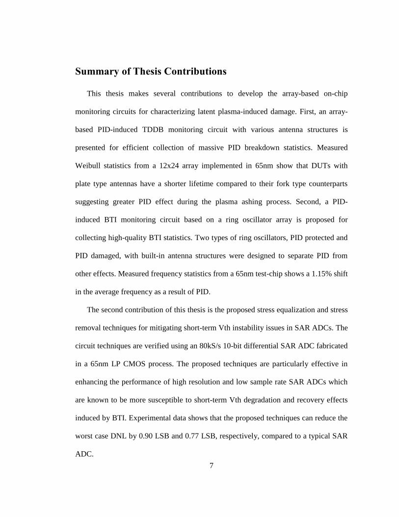
2.2 Prior Work on PID Characterization
In this section, we summarize previous approaches for characterizing PID
effects and point out their pros and cons. The gate-leakage current or threshold voltage
of fresh devices was measured in [1, 4-6, 9, 11] which is a simple and fast method for
characterizing PID, but this method suffers from low sensitivity. Comparing the
TDDB lifetime under constant voltage stress (Fig. 2.4) for PID damaged and PID
protected devices can provide information on the amount of underlying PID. This
method has a simple test structure consisting of just two different device types.
However, the limited sensitivity and long test time of over 1000 seconds per sample
make this method unfit for massive data collection [4, 6-9]. A ramped stress voltage
was used for TDDB lifetime measurements in [4] to reduce the TDDB test time to 2
seconds per sample, but the correlation with the standard TDDB results under a
constant stress voltage has not been fully understood. Finally, the residual BTI lifetime
(Fig. 2.4) can be used as a signature for latent PID effects. Previous studies in [7]
reported that latent PID leads to an increase in long-term threshold voltage shift due to
the BTI mechanism. Despite the higher sensitivity compared to the TDDB approach,
only limited data has been reported so far as fast unwanted BTI recovery has made it
difficult to collect high-quality BTI statistics [7-9, 12]. PID-induced BTI lifetime
projection (Fig. 2.5) involves massive BTI statistics collection for AR, stress voltage,
and stress temperature projections that helps to optimize the plasma process and find
proper operating conditions. In addition, obviously, a combination of the efficient
TDDB and BTI statistical measurement methods may have to be considered in order
to fully understand the impact of latent PID on device and circuit reliability.
15
Pros
Cons
Impact of
latent PID
BTI Test
High sensitivity
Short test time
Difficult to collect high
quality data (fast BTI,
unwanted recovery)
Increased ∆Vth
Mechanism
n+ p+ n+ p+Si
H
+Si
H
Si
H
VDD
*NBTI Stress
+
n+ p+ p+Si
H
Si
H
Si
H
VDD
*NBTI Recovery
+
VDD
VDD
n+
Time 0
Trap
Time 1
Conduction Path
Time 2
ConductiveFilament
p+ n+ p+
Gate dielectric
TDDB Test
Lower sensitivity
Longer test time
Relatively simple test
cell structure
Shorter time-to-breakdown
VDD VDD
*Negative Bias Temperature Instability
Fig. 2.4. Characterizing latent PID: BTI vs. TDDB tests. Both mechanisms have to be
considered together in order to fully understand the impact of latent PID on device and
circuit reliability.
101
102
103
104
105
106
107
108
109
1010
0 3 5
PID
-In
du
ce
d B
TI L
ife
tim
e (
s)
Voltage (V)
AR2 AR1
Operating Lifetime: 10yrs
1 2 4
VNOM VMAX, AR2
VMAX, AR1
(AR1 > AR2)
Fig. 2.5. PID-induced BTI lifetime projection involved collecting massive amounts of
data under different Antenna Ratios (ARs), stress voltages, and stress temperatures.

16
Single device probing
Wafer probe system
Array-based circuit system
Single device probing
Array-based circuit system
Meas.
time
1
Wafer
area
1
*1/n2 *1/n
2
Measurement
Off-chip tester
On-chip current to digital
Scalability
No
Yes
*nxn array, parallel stress
Fig. 2.6. High level comparison between device probing vs. array-based
characterization [10, 23].
2-D array 2-D arraySingle device
Parameter of
interestTDDB
Initial ΔVth
Increased ΔVth
TDDBIncreased Δf
Schematic
Measurement
resolutionLimitedHigh High
Sampling
Time
Short
(Parallel stress)
Long
(Serial stress)
Short
(Parallel stress)
Circuit based systemDevice probing
Measurement
time
Depends on tester speed
(several milliseconds)N/A
Short time interruption
(>1μs*)
An
ten
na
BL
IG
Current-to-digital converter
Counting number
* For a 0.01% frequency shift Resolution and a ROSC period of 10ns, enable to minimize the unwanted BTI recovery
Beat frequency detection
system
Counting number
SmallLarge SmallSilicon area
1-D array
Initial ΔVth
High
-
(No stress purpose)
Depends on I/O BW
(several milliseconds)
Small
An
ten
na
S
GD
An
ten
na
ID
Note: one stress cell is shown
D
G
S
An
ten
na
G
An
ten
na
`
An
ten
na
An
ten
na
An
ten
na
f BL
[5, 11] [10][1, 4, 6, 7-9, 12] [23]
Cell feature
Fig. 2.7. Comparison with previous PID characterization methods.

17
In terms of the test structure design for collecting large device statistics, one
can consider using traditional device probing or on-chip array-based circuit system
(Fig. 2.6). Traditional device probing [1, 4, 6, 7-9, 12] is widely used due to
simplicity, but collecting massive statistical TDDB or BTI data is cumbersome and
time-consuming since only few devices can be stressed at the same time. Array-based
circuit system in [10, 23], on the other hand, can reduce the test time and test silicon
area by a factor proportional to number of devices in the array, since we can stress all
the cells in parallel while cycling through each cell to measure TDDB or BTI
degradation. Furthermore, an array format can be easily scaled up to collect statistical
data from a massive number of devices. With these benefits in mind, a 1-D device
array illustrated in Fig. 2.7 (second row) was demonstrated in [5, 11] to reduce the
silicon area. To overcome the long stress time required for the 1-D array, a 2-D array
in [10] (Third row in Fig. 2.7) is proposed where the gate leakage current was
monitored using an on-chip current-to-digital converter for measuring TDDB lifetime
in this work. DUTs in the 2-D array can be stressed in parallel while taking fast serial
measurements administered through a convenient scan based interface. This feature
reduces the test time and silicon area by a factor proportional to the number of DUTs.
Another focus of this work (fourth row in Fig. 2.7) is on measuring BTI degradation
from an array of ring oscillator circuits that have undergone PID damage. We compare
the results with the BTI degradation measured from another group of ring oscillators
that are insensitive to PID to extract just the PID-induced component. Traditionally,
characterization of PID-induced BTI degradation involved continuously monitoring
the threshold voltage shift for a large population of devices using individual device

18
probing [7-9. 12]. The device probing method shown in Fig. 2.6, however, is time-
consuming and cumbersome due to the serial stress as mentioned earlier. Furthermore,
especially for the BTI measurement case, the test setup has to support fast
measurements (e.g., within a microsecond) to suppress unwanted BTI recovery. This
requires an elaborate setup in which the device is periodically taken out of stress,
measured under a nominal supply, and then switched back to a stress mode. To
overcome these issues, in this work, a 2-D ROSC array [23] was designed capable of
applying parallel stress to all devices in the array while achieving a sub-microsecond
measurement time using the tested-and-proven Beat Frequency (BF) detection scheme
[16-22]. Another benefit of the proposed design over traditional device probing is that
we can directly measure how PID affects circuit frequency and its degradation over
time.

19
2.3 Proposed PID-induced TDDB Characterization Circuit
Design
2.3.1 Test DUT Array Design
The proposed array-based PID TDDB characterization circuit [10] shown in Fig.
2.8 consists of 12x24 stress cells, an on-chip current-to-digital converter, a Finite State
Machine (FSM) control logic, column/row select circuits, and a scan interface.
Although both thin oxide and thick oxide devices can be considered for the DUT, we
chose to use the latter option as experimental data indicate that devices with oxides
thinner than 2nm are more tolerant to PID effects [7]. Each stress cell contains an
NMOS DUT with an oxide thickness of 5.0nm. Each DUT has a dimension of
W=0.4µm, L=0.24µm. No protection diodes are connected to the gate of the NMOS
transistors. The higher stress voltage (typically 3-4 times the IO supply) and lack of an
even thicker oxide device complicate the design of the stress cell implemented with
I/O devices only [24]. A stack of two blocking circuits with dynamic biasing shown in
Fig. 2.9 was employed to protect stress cell circuits from the high stress voltage
(VSTRESS). It was sufficient for the ~6.5V stress voltage that was to keep the
measurement time small. An off-chip VSTRESS voltage was applied through a
dedicated pad. The gate of DUT is connected to various antenna structures. Reference
DUTs with no antennas are also implemented for comparison purposes. Gate current
(IG) of each DUT is measured sequentially through a global BitLine (BL) while the
entire array is being stressed in parallel.

20
24
12
BL
FSM Current-to-digital converter
Logic Analyzer, Labview® interface
One set of
Stress Cells
One set of
Stress Cells
One set of
Stress Cells
One set of
Calib Cells
Column periph.
Ro
w p
eri
ph
.
Count2InitiateADR_CLK
Scanout CLK
FR
ES
H
RE
XT
Fig. 2.8. Diagram of the proposed array-based PID TDDB characterization circuit [10].
One set of stress cells have three stress cells (i.e. two cells with antennas (plate and
fork type) and one reference stress cell without an antenna). We were limited to 288
ROSC cells in the array due to silicon area constraints, but this design could be
expanded to include many more stressed ROSCs.
B
L (
Re
ad
ou
t p
ath
)VSTRESS
VB
DFFDQ
FRESH
ROWCOL
ME
AS
STR
Antenna structureDUT
VB
Blo
ck
ing
cir
cu
it
(Po
st-
bre
ak
do
wn
)
IG
(2~3 times nominal supply)
TOP
Fig. 2.9. Single stress cell including DUT, antenna, and control circuits. A thick oxide
NMOS is used as a DUT. A blocking circuit was used to protect non DUT devices.

21
2.3.2 On-chip Current-to-Digital Converter and Test Procedure
To measure the IG of each DUT, we adopted an on-chip current-to-digital
converter in [24] shown in Fig. 2.10. The BL voltage is first pre-discharged and then
pulled up by IG. Any progressive TDDB behavior in the form of IG is converted to a
digital count by the on-chip current-to-digital converter. An optional IREF is used to set
the minimum count output. The dual reference comparator senses the CEXT charging
time from ‘START’ to ‘END’ times for the counting operation. The count value is
loaded into a shift register and serially read out through a convenient scan interface. A
LabVIEWTM program compares the count with a user defined threshold and asserts a
FRESH signal which prevents further stressing in case the cell is broken. A calibration
cell and an external resistor (REXT) in Fig. 2.8 are used to translate the measured count
to an absolute resistance value.
ADR_CLK
VCO
16b Counter
16b parallel/serial
shift register
16
Count
CLK
CEXT
VREFH
END
VDDH domain
VDDL domain
RST
DISCHARGE
Level
conv .
VREFL
StartIREF
BLIG
IREF+IG
VBL
Fig. 2.10. On-chip current-to-digital converter for monitoring soft and hard
breakdown events in the DUT cell. IG of each DUT measured sequentially and
converted to a digital count and read off-chip.
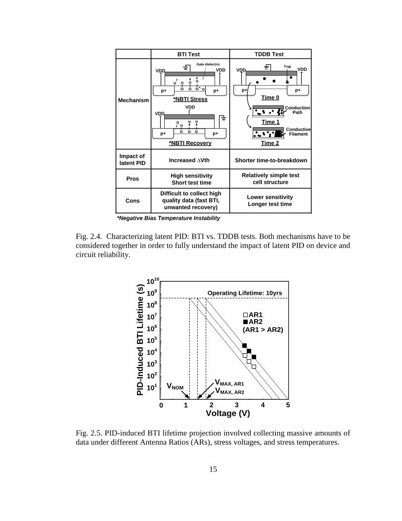
Measurements are automated through a simple digital scan interface as shown in
Fig. 2.11. A RESET signal is asserted by Initiate signal before stress conditions are set
22
which prevents any cells from being selected. During experiments, DUT cells are
cycled through automatically without the need to send or decode cell addresses, in
order to simplify the logic and attain faster measurement times. Each DUT cell is
selected by ADR_CLK for a new charging time measurement, then DISCHAGE signal
is triggered to discharge the CEXT. The row selection signal is incremented with each
measurement, and the column selection shifts after all of the cells in a row have been
tested. This process is repeated through the rows and columns as necessary. The
measured charging time of BL voltage from the rising edge of START signal to the
falling edge of END signal is converted to a digital count number by the on-chip
current-to-digital converter. After the counts are generated, The COUNT is the read
out by the LabVIEWTM program.
Initiate
ADR_CLK
Resetb_FF
DISCHARGE
Internal_
ROW_CLK
VREFLBL
Count
generation
END Count
read out
Scanout_
CLK
COUNT
16
FRESH
VREFH
START
1: Fresh, 0: Broken
Fig. 2.11. Waveforms illustrating the basic operation of the proposed PID-Induced
TDDB characterization circuit. In this waveforms, the operation of first selected cell
is only shown for simplicity. External I/O signals indicated by blue lines.

23
2.3.3 Antenna Design
Plate and fork type antenna structures with AR values of 10k and 20k were
implemented (Fig. 2.12). Among various candidates, we selected these two antenna
topologies to compare the PID effect in an area-extensive antenna (plate type) versus a
perimeter-extensive antenna (fork type). The number of DUTs for each antenna
topology is given in Fig. 2.12 (c). Although we were only able to include 64 or 32
DUTs for each antenna type due to the limited silicon area and the large antenna
footprint, the proposed array design can be easily scaled up to collect. The layout view
of the three stress cells (i.e. plate antenna, fork antenna, no antenna) is shown in Fig.
2.13. M5-M6 layers were dedicated to the antenna structures while portions of M2-M4
were used for antennas due to the areas reserved for the signal and power routing
tracks. For the same AR, the fork antenna requires a larger silicon area than the plate
antenna due to the metal fingers. Rather than increasing the stress cell area which will
result in an unnecessarily large test-chip, we utilize the empty space in the adjacent no
antenna DUT cell for the large fork antenna. Usage of each metal layers in the test-
chip are listed in Fig. 2.14. To maximize the utilization of the metal layers and to
achieve a dense chip implementation, we fill the empty areas of M2-M6 with antenna
structures. Note that M1 to M4 layers were used for the signal and power routing
tracks. The top surface areas for each metal layer along with the total antenna area are
given in Fig. 2.15. Since we want each DUT to be affected by the plasma charge
acting on its own antenna in M2-M6, a small jumper line on M7 was used as the
global VSTRESS node as shown in Fig. 2.16. This well-known method prevents the
global node from connecting to the DUTs prior to the M7 metal formation resulting in

24
a realistic PID damage scenario. The cumulative ARs of the DUTs are given in bottom
of Fig. 2.16. The AR due to the vias and contacts were negligible and therefore were
omitted in the calculation. Note that each DUT has the same number of vias and
contacts. Due to the small metal area of the M7 jumper and the large number of DUTs,
PID due to the M7 layer itself can be ignored.
AR=10k AR=20k
DUT with plate type
antenna64ea
64ea
32ea
32ea
Reference DUT without antenna : 96ea
DUT with fork type
antenna
(a) (b)
(c)
Fig. 2.12. Conceptual view of (a) the plate and (b) fork type antenna structures
implemented in the test array. Each antenna consists of 5 metal layers (M2-M6). Only
one metal layer is shown here for simplicity. The fork type antenna consists of metal
fingers and hence occupies a larger silicon area than the plate type antenna with the
same AR. (c) The number of DUTs for each antenna type.

25
STRESS
TR
1.0
5u
m
M5M7 M4
Plate antenna cell
(1) (4)(3)(2)(1)
(1)DUT
(1)(2)(3)(4)
DUTDUT
Fork antenna cell No antenna cell
Plate antenna region Fork antenna region
Fork antenna extension
Plate antenna :
171.2um2
Fork antenna:
171.2um2
(3) VSS
(4) BL
(1) VSTRESS
(2) VDD
(a)
1.0
5u
m
(1) (4)(3)(2)(1)
(1)
(1)(2)(3)(4)
DUT DUTDUT
M5M7 M6
Plate antenna cell Fork antenna cell No antenna cell
Plate antenna region Fork antenna region
Fork antenna extension
Plate antenna :
316.72um2
Fork antenna:
316.72um2
(3) VSS
(4) BL
(1) VSTRESS
(2) VDD
(b)
Fig. 2.13. Layout view of three stress cells (i.e. two cells with antennas and one
reference stress cell without an antenna). (a) M4 layer and (b) M6 layer views shown.
Empty back end areas were filled with antenna structures for a compact array design.

26
Signal routing AntennaMetal layer
M7
O
O
O
O
Jumper
O
M5 ~ M6
M2 ~ M4
M1
Fig. 2.14. Metal layer usage in the 65nm PID characterization test-chip.
AR=10k AR=20k
M5, M6
M2, M3, M4
Total antenna area
of each DUT
AR (Antenna Ratio)
316.72µm2
171.2µm2
1147.04µm2
10241 23234
607.76µm2
462.24µm2
2602.24µm2
Fig. 2.15. Antenna area of each metal layer and total Antenna Ratio (AR). Thick
oxide NMOS devices used for the DUT have a dimension of W=0.4µm and
L=0.28µm.
M1
M2
M3
M4
M5
M6
M7
(3) DUT w/o
antenna
(1) DUT with
plate antenna
(2) DUT with
fork antenna
VSTRESS
An
ten
na
Ju
mp
er
A small M7 jumper line
connects the antenna
nodes for VSTRESS
Area(M2-M6) Area(M7)AR(1,2)
Area(Gate) Area(Gate) (12 24)
Area(M7)AR(3)
Area(Gate) (12 24)
Fig. 2.16. Cross-sectional view of antenna structure including a small M7 jumper
connection for the common VSTRESS signal (top). Antenna ratio calculation (bottom).

27
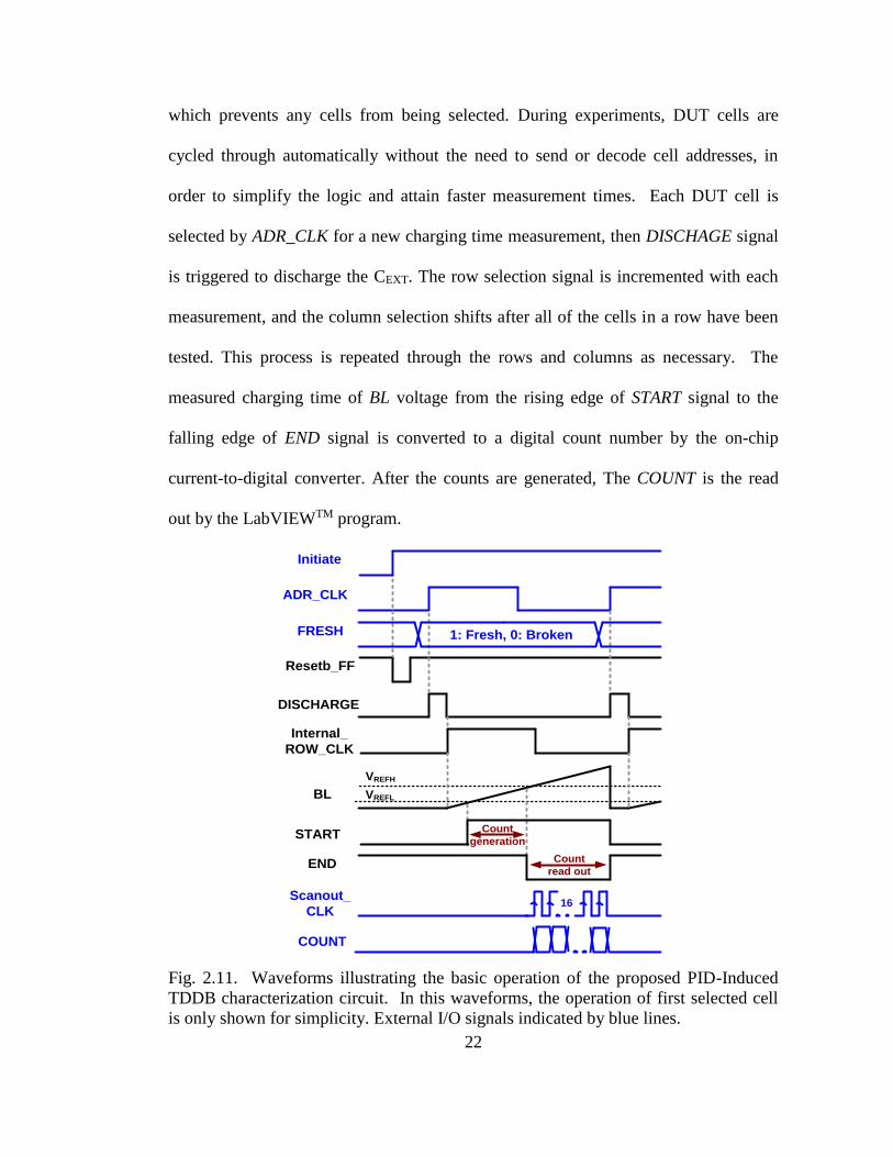
2.3.3 Statistical Breakdown Measurement Results
Fig. 2.17 shows the measured time-to-breakdown data in Weibull scale for DUTs
with different antenna structures stressed at 6.5V and 6.7V. The cumulative time-to-
breakdown curves shift to the left for DUTs with larger antennas indicating an
increased PID for gate dielectrics connected to larger antennas. The normalized Mean
Time to Failure (MTTF, 63 percentile point) data under a 6.5V stress voltage in Fig.
2.18 shows that the fork (or plate) antenna with AR=10k has a 7.7% (or 10.2%)
shorter lifetime compared to a reference device with no antennas attached. Time-to-
breakdown measured from different chips shows a consistent trend as shown in Fig.
2.19. A DUT with a plate type antenna shows a consistently shorter lifetime compared
to its fork type counterpart. Fork antennas have a larger perimeter surface area
compared to plate antennas and hence become more susceptible to plasma damage
during the etching process. However, our measured data shows the opposite trend with
plate antennas having shorter lifetimes. This suggests that PID during the etching
process is relatively small compared to that during the ashing process. Note that the
charge build up during ashing is facilitated when the resistance from the charge
collecting surface to the gate dielectric is smaller as in the case of plate antennas. The
die photograph of the 65nm test-chip is shown in Fig. 2.20.
28
-5
-4
-3
-2
-1
0
1
2
8 9 10
ln(-
ln(1
-cd
f))
Time (ln (a.u))
No antenna
Plate (10k AR)
Fork (10k AR)
Plate (20k AR)
Fork (20k AR)
6.5V, 26°C
-5
-4
-3
-2
-1
0
1
2
6.5 7.5 8.5
Time (ln (a.u))
No antenna
Plate (10k AR)
Fork (10k AR)
Plate (20k AR)
Fork (20k AR)
6.7V, 26°C
ln(-
ln(1
-cd
f))
Fig. 2.17. Measured breakdown data in Weibull scale for devices with different
antenna topologies. Results are shown for two stress voltages; 6.5V (left) and 6.7V
(right).
75
80
85
90
95
100
6.5 6.7
No antenna
Fork (10k AR)
Plate (10k AR)
Fork (20k AR)
Plate (20k AR)
65nm, 26°C
MT
TF
(6
3%
, n
orm
alize
d)
VSTRESS(V)
Fig. 2.18. Normalized MTTF for devices with different antenna topologies stressed at
6.5V and 6.7V.
70
75
80
85
90
95
100
105
#5 #6 #7 #8
No antenna
Fork (10k AR)
Plate (10k AR)
Fork (20k AR)
Plate (20k AR)
MT
TF
(6
3%
, n
orm
alize
d)
6.7V, 26 C
Chip #
75
80
85
90
95
100
105
#1 #2 #3 # 4
No antenna
Fork (10k AR)
Plate (10k AR)
Fork (20k AR)
Plate (20k AR)
6.5 V, 26 C
MT
TF
(6
3%
, n
orm
alize
d)
Chip #
Fig. 2.19. Time-to-breakdown measured from different chips shows a consistent trend.

29
Ro
w p
eri
ph
.
Column periph.
12x24 DUTs with and
without antennas
Current-to-digitalconverter
VDDL decap
VDDH
decap
65nm LP CMOS
VDD (core/IO) 1.2V / 2.5V
Stress Condition
Circuit Area
6.5V, 6.7V @ 26ºC
0.65x0.36mm2
Process
Fig. 2.20. Die photo and summary of the array-based PID TDDB characterization
chip.

30
2.4 Proposed PID-induced BTI Characterization Circuit
Design
The proposed PID-induced BTI characterization circuit [23] shown in Fig. 2.21
consists of ROSC cells, a finite state machine (FSM), a scan based test interface, and
three BF detection systems. Details of each block and the different antenna structures
will be provided in the later sections. The array consists of only 40 ROSC cells due to
the limited silicon area available in the multi-project wafer chip, but the design can be
readily expanded to larger array sizes. Two types of ROSCs, a PID protected ROSC
and a PID damaged ROSC, were designed using different antenna configurations. The
reference ROSCs are identical to the PID protected ROSCs in the test array.
Either the entire array or a section of the array can be selected for applying stress
voltage while a single cell is taken out of stress for measuring the ROSC frequency
shift. During stress mode, the ROSCs are in an open loop configuration so that each
inverter stage can be stressed by a DC VSTRESS voltage. When each oscillator is
selected for a measurement with the MEASSTRESS signal from the controlling
software, its supply is set to the I/O device nominal voltage level of 2.5 V, the loop is
closed, and its frequency shift is measured by three BF detection systems. Three
reference ROSCs are trimmed to the positions within the fresh array distribution so
that we can maximize the measurement resolution of the BF detection circuit [20, 21].
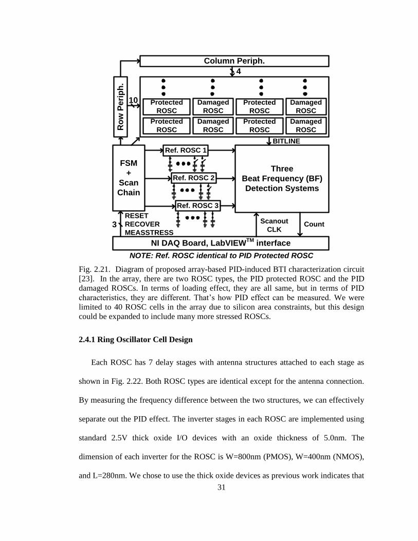
31
Ro
w P
eri
ph
.
Column Periph.
Ref. ROSC 1
Three
Beat Frequency (BF)
Detection Systems
Count
FSM
+
Scan
Chain
Ref. ROSC 2
Ref. ROSC 3
BITLINE
NOTE: Ref. ROSC identical to PID Protected ROSC
NI DAQ Board, LabVIEWTM
interface
4
10
Protected
ROSC
Damaged
ROSC
Protected
ROSC
Damaged
ROSC
Protected
ROSC
Damaged
ROSC
Protected
ROSC
Damaged
ROSC
RESET
RECOVER
MEASSTRESS3 Scanout
CLK
Fig. 2.21. Diagram of proposed array-based PID-induced BTI characterization circuit
[23]. In the array, there are two ROSC types, the PID protected ROSC and the PID
damaged ROSCs. In terms of loading effect, they are all same, but in terms of PID
characteristics, they are different. That’s how PID effect can be measured. We were
limited to 40 ROSC cells in the array due to silicon area constraints, but this design
could be expanded to include many more stressed ROSCs.
2.4.1 Ring Oscillator Cell Design
Each ROSC has 7 delay stages with antenna structures attached to each stage as
shown in Fig. 2.22. Both ROSC types are identical except for the antenna connection.
By measuring the frequency difference between the two structures, we can effectively
separate out the PID effect. The inverter stages in each ROSC are implemented using
standard 2.5V thick oxide I/O devices with an oxide thickness of 5.0nm. The
dimension of each inverter for the ROSC is W=800nm (PMOS), W=400nm (NMOS),
and L=280nm. We chose to use the thick oxide devices as previous work indicates that

32
devices with thicker oxides are more susceptible to PID effects [7]. However, the
proposed characterization method would be equally useful and perhaps more effective
for thin oxide devices if larger arrays (e.g., 1000’s of cells) can be built.
The supply voltage (SUPPLY) of each ROSC can be independently switched
between stressed voltage (VSTRESS), nominal supply (VDD), and 0V using the on-
chip power gates depicted in Fig. 2.22. This allows us to collect both the fresh and
stressed frequency distributions. The ROSC is first disconnected from the BITLINE to
prevent any unwanted stress in other parts of the array. During stress, the ROSC loops
are opened so that VSTRESS can be applied to the ROSC devices. During the
measurement mode, the supply voltage of the selected ROSC is switched to a VDD
using the power gate while the other ROSCs are kept in the stress mode. Subsequently,
the M/S signal is asserted and the selected ROSC generates a frequency output which
is paired with a fresh reference. Note that the reference ROSCs are kept fresh (i.e., 0V
supply) during the long stress periods and are only activated (i.e., VDD) during the
short measurement times.
6 bit trimming caps
Antenna Antenna Antenna Antenna Antenna AntennaAntenna
Output Stages
SUPPLY SUPPLY SUPPLY SUPPLY SUPPLY SUPPLY SUPPLY
SH
AR
ED
BIT
LIN
E
I/O device (tox: 5nm)
1 (measurement)
0 (stress)
SUPPLY
VDDVSTRESS
SUPPLY Switch Block
PBTI stress on NMOS
NBTI stress on PMOS
M/S
M/S
M/SM/S M/S
RECOVER
M/S
P: 800/280nm
N: 400/280nmROSC DUT Dimensions
Fig. 2.22. Schematic of PID protected and damaged ROSCs. Aside from the antenna
connection (Fig. 2.25), the two ROSCs are identical and thus any difference in
measured frequency can be attributed to PID. All transistors are thick oxide I/O
devices (indicated by double lines).

33
2.4.2 Beat Frequency Detection System
The Beat Frequency (BF) detection system shown in Fig. 2.23 is an all-digital
differential system that measures frequency degradations in the stressed (PID
protected or PID damaged) ROSCs with resolution and measurement times
theoretically ranging down to 0.01% and 1μs, respectively. Details of the BF
detection technique can be found in many previous publications [16-22]. A BF
detection system provides high-resolution frequency shift measurements when the
frequencies of two free-running ROSCs are close (e.g., <1%), which can be ensured
using trimming capacitors shown in Fig. 2.22. The basic operating principle is shown
in Fig. 2.23. A 1% shift in stressed frequency (B1→B2) is amplified to a 50% change
in the output count (N1→N2). The high resolution combined with the short
measurement time makes this technique ideal for BTI measurements where unwanted
BTI recovery must be suppressed. Adding trimming capacitors to every single ROSC
in the array and programming them individually would be time and area consuming.
Therefore, we opted to hardwire three of six capacitors “on” in each of those ROSCs,
while individually controlling all six in the three references. The stressed ROSC
frequency is compared with the three reference ROSC frequencies, generating three
count values for each BF measurement [20, 21]. We use the highest count of the three
to calculate the actual % frequency shift. During calibration, the three reference
ROSCs are trimmed to positions within the fresh array distribution such that we
maximize the frequency measurement resolution for the entire array throughout the
entire stress experiment.

34
B
A
C
fref : Constant 1.00GHz
N1=100
N2=50
Stressed ROSC
(PID Protected or
Damaged ROSC)
Reference ROSC
(PID Protected ROSC)
C1
C2
A
B1
B2
fstress1 : 0.99GHz (Before stress)
fstress2 : 0.98GHz (After stress)
Phase
Comp.
PC_OUT (fbeat = fref - fstress)
8-bitCounter
5-bit
Majority Vote
(rejects
bubbles)
Edge
Detector
(find rising
edge of
PC_OUT)
Parallel/Serial Shift Register
Count:
reset8b
Fig. 2.23. The beat frequency detection system achieves a high frequency shift
precision (>0.01%) and a short (>1μs) stress interrupt time for precise BTI
measurements [16-22].
2.4.3 Test Interface and Procedure
Measurements are automated through a simple digital scan interface as shown in
Fig. 2.24. First, we sweep the trimming capacitors in three reference ROSCs and
average the measured frequency values from the 40 ROSCs in the array. The
reference ROSC frequencies are then separated out using trimming capacitors to cover
the distribution of frequencies of the ROSCs to be tested.
A RESET signal is asserted before stress conditions are set which prevents any
cells from being selected, and puts them all into recovery mode as mentioned earlier.
During experiments, ROSC cells are cycled through automatically without the need to
send or decode cell addresses, in order to simplify the logic and attain faster
measurement times. The first cell is selected with an initialization sequence, and
MEASSTRESS is asserted each time the controlling software is ready for a new

35
measurement. The row selection signal is incremented with each measurement, and
the column selection shifts after all of the cells in a row have been tested. This process
is repeated through the rows and columns as necessary. Any cells that have not been
selected for stress are kept in a 0V no-stress state by asserting the RECOVER signal
appropriately. The supply voltage of the selected ROSC is switched to a VDD and
frequency shift of the ROSC are measured through a shared BITLINE. The measured
frequency shift is converted to a digital count number by the three BF detection
systems. After the counts are generated, MEASSTRESS goes low and the selected
ROSC is disconnected from the BITLINE and the supply voltage of the selected
ROSC is switched to VSTRESS putting the ROSC devices back into stress mode. The
COUNT is the read out by the LabVIEWTM program.
RESET
MEASSTRESS
Resetb_FF
Internal
ROW CLK
BITLINE
SCANOUT
StartCount
read out
SCANOUT
CLK
COUNT
24
RECOVER
Row0, Col0 cell
SUPPLYVDD
VSTRESS
Row1, Col0 cell
SUPPLYVDD
VSTRESS
Row0, Col0 cell
selectRow1, Col0 cell
select
Count
read out
24
Count
Generation
by 3 BF detection
systems
Count
Generation
by 3 BF detection
systems
Fig. 2.24. Waveforms illustrating the basic operation of the proposed PID
characterization circuit. In this waveforms, the operation of first two selected cells
with “low” RECOVERY case is only shown for simplicity. External I/O signals
indicated by blue lines.

36
2.4.4 Antenna Design
Several studies show that the degree to which PID affects device reliability is a
function of not only the AR, but also the topology of the antenna structure [4-7, 10-11].
Unfortunately, due to area limitations, we could not implement different antenna
topologies to study any layout dependencies. Plate type antennas shown in Fig. 2.25
were the only ones we could implement as a proof of concept. However, other antenna
topologies (e.g., fort type antenna structure in previous PID-induced TDDB
characterization circuit) can be considered in future designs.
Since we want only the PID damaged ROSC to be affected by the plasma charge,
we adopted a jumper technique in which the position of a small M7 jumper was
interchanged in the two ROSC types. In this way, PID damage is protected in the load
transistors which are connected to antennas through a jumper structure. In contrast,
PID damaged ROSCs are affected by PID since plasma charge is directly applied to
the gate dielectric of the load transistor. Fig. 2.26 shows the simulated frequencies of
both types of ROSCs from post-layout RC extracted netlists indicating a negligible
frequency difference of 0.02MHz or 0.0067%. This confirms that any frequency
difference greater than this amount can be attributed to PID. The metal layer usage and
top surface areas for each metal layer along with the total antenna area are listed in
Figs. 27 and 28. To maximize the antenna metal surface area in our tiny test-chip, the
antenna utilizes a vertical M2-M6 metal stack with numerous VIAs in between the
different layers. Here, M5-M6 layers were dedicated to the antenna structures while

37
portions of M2-M4 were used for antennas due to the areas reserved for the signal and
power routing tracks. The total AR is 4,464 for the metal wires and 721 for the VIAs.
M1
M2
M3
M4
M5
M6
M7
Plate antennas
VIASmall Jumper
Plate antennas
(a) (b)
Driver ReceiverDriver Receiver
Small Jumper
Plate
Antenna
M2-M6
Plate Antenna
M2-M6
GND Shielding
Small
Jumpers
VIA
Plate
Antenna
(c) (d)
Fig. 2.25. Cross-sectional, schematic and layout view of a single stage of (a, c) PID
protected ROSC and (b, d) PID damaged ROSC. We adopted a jumper technique in
which the position of a small M7 jumper is changed in the two ROSC types. In this
way, PID damage is protected in the load transistors which are connected to antennas
through a jumper structure in PID protected ROSCs. In contrast, PID damaged ROSCs
are indeed affected by PID since a plasma charge can discharge only through the gate
dielectric of the load transistor.

38
292
294
296
298
300
302
0 0.05 0.10 0.15 0.20 0.25 0.30
Fre
qu
en
cy
(M
Hz)
Time (μs)
PID Protected ROSCs (Avg.: 297.58MHz)
PID Damaged ROSCs (Avg.: 297.60MHz)
Post Layout, VDD=2.5V, TT, 26ºC
Avg. Frequency Difference w/ No PID:
0.02MHz (0.0067%)
Fig. 2.26. Simulations showing negligible frequency difference between the two
ROSC types. This confirms that any frequency difference measured from the test-chip
is due to PID rather than process variation.
Signal routing AntennaMetal layer
M7
O
O
O
O
Jumper
O
M5 ~ M6
M2 ~ M4
M1
Fig. 2.27. Metal layer usage in the 65nm PID-induced BTI characterization test-chip.
Metal VIA
M5, M6
M2, M3, M4
Total antenna area
of each DUT
AR (Antenna Ratio)
300µm2
300µm2
1500µm2
4464 721
43.15µm2
52.07µm2
242.52µm2
total surface area of antenna structure
gate areaAR =
Fig. 2.28. Antenna area of each metal layer and total AR. Thick oxide devices used
for the ROSC have a dimension of W=800nm (PMOS), W=400nm (NMOS) and
L=280nm.

39
2.4.5 Statistical Frequency Measurement Results
A test-chip was fabricated in a 65nm CMOS process and measurements were fully
automated through a data acquisition board controlled by LabVIEWTM software. Fig.
2.29 shows the measured fresh frequency distributions for both types of ROSCs. The
average fresh frequency of PID damaged ROSCs is 1.15% lower than that of the PID
protected ROSCs. A consistent trend is measured across different chips. Fig. 2.30
shows the measured frequency distributions after a 1000-second DC stress session,
along with the fresh distributions under 3.6V and 4.0V stress voltages. The
degradation of the average frequency for the PID protected ROSCs and PID damaged
ROSCs are 2.5% and 4.4%, respectively, for 3.6V stress voltage. Similar trends are
measured for stress voltage of 4.0V. Our experiment results confirm that circuits
undergo PID-induced BTI degradation even before they are used and suggest that a
higher concentration of weak Si-H bonds at the dielectric interface were generated by
PID in our test devices. Fig. 2.31 shows the measured mean and standard deviation of
the frequency shifts (i.e., Δf) at 3.6V and 4.0V stress voltages. The mean and standard
deviation of the frequency shift for both ROSC types follow power law dependency.
The time slope of the mean is measured to be roughly twice that of the standard
deviation. Fig. 2.32 compares measured PID-induced BTI lifetime for PID protected
and PID damaged ROSCs as a function of the stress voltage. We observe that the
projected VMAX of PID damaged ROSC is smaller than that of PID protected ROSC.
The die photo and chip summary of the 65nm test-chip are shown in Fig. 2.33.

40
0
5
10
15
20
25
30
35
40
236 238 240 242 244 246 248 250
Oc
cu
rre
nc
es
(%
)
ROSC Frequency (MHz)
μ=241.6σ=1.8263
μ=244.4σ=1.6511
PID Protected ROSCs-
PID Damaged ROSCs
Fresh, 26 CO
1.15% Avg.
frequency (μ)
degradation
0
0.4
0.8
1.2
1.6
2
2.4
#1 #2 #3 #4 #5 #6 #7 #8 #9Chip #
Fre
qu
en
cy
Sh
ift
Me
an
(%
)
Max: 1.39%
Min: 0.88%
Freq(protected)– Freq(damaged)
Fresh, 26 CO
(a) (b) Fig. 2.29. (a) Measured fresh frequency distributions show a 1.15% degradation in
average frequency as a result of PID. (b) Degradation in the average fresh frequency
measured from different chips shows a consistent trend.
Oc
cu
rre
nc
es
(%
)
FreshAfter 1000s Stress
3.6V DC Stress, 26 C
ROSC DUT Frequency (MHz)
μ =231.2σ =2.2528
FreshAfter 1000s Stress
μ=241.9σ=1.7921
PID Protected ROSCs
PID Damaged ROSCs
O
Decreased μ (2.5%)
Increased σ
Decreased μ (4.4%)
Increased σ
0
5
10
15
20
25
30
35
40
220 225 230 235 240 245 250
μ =238.5σ =1.9183
μ=244.8σ=1.6218
0
5
10
15
20
25
30
35
40
220 225 230 235 240 245 250
Oc
cu
rre
nc
es
(%
)
μ=230.2σ=2.3682
μ =243.9σ =1.6812
4.0V DC Stress, 26 C
FreshAfter 1000s Stress
PID Protected ROSCs
PID Damaged ROSCs
O
ROSC Frequency (MHz)
μ =219.3σ =2.7251
FreshAfter 1000s Stress
μ =241.1σ =1.8577
Decreased μ (5.6%)
Increased σ
Decreased μ (9.0%)
Increased σ
0
5
10
15
20
25
30
35
40
210 215 220 225 230 235 240 245 250
0
5
10
15
20
25
30
35
40
210 215 220 225 230 235 240 245 250
(a) (b)
Fig. 2.30. Frequency distribution before and after a 1000 sec, (a) 3.6V and (b) 4.0V
DC stress session for PID protected and PID damaged ROSCs.
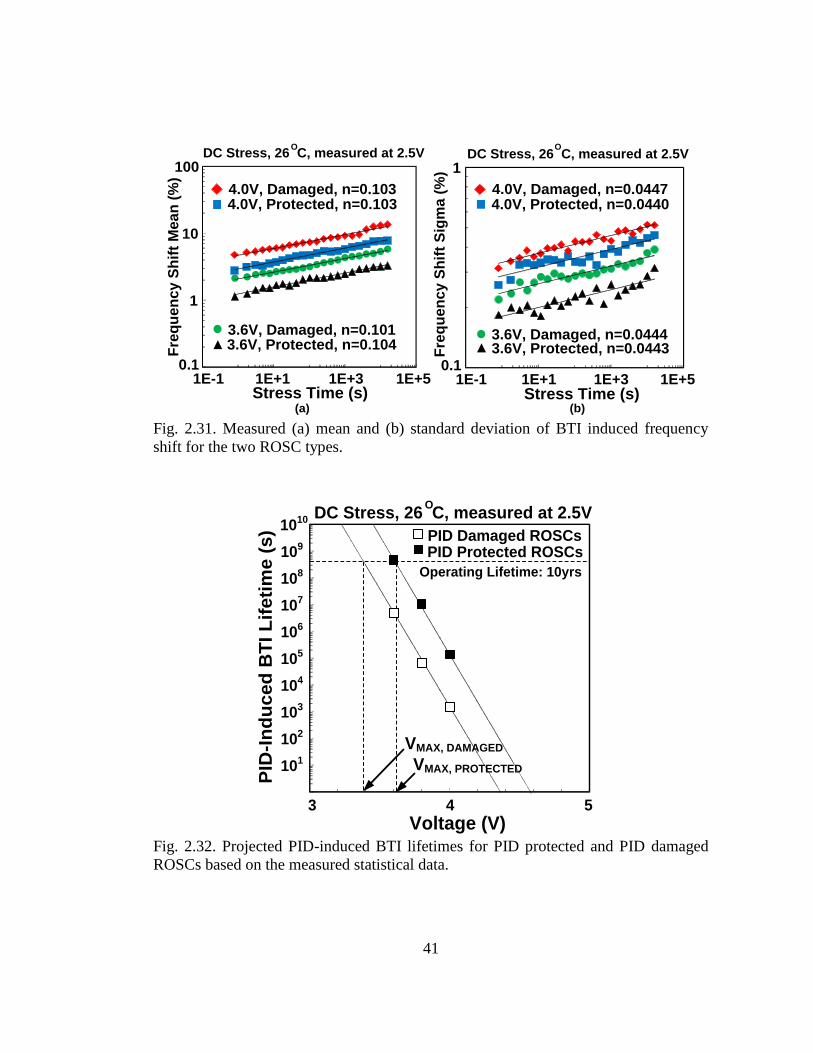
41
0.1
1
1E-1 1E+1 1E+3 1E+5
Fre
qu
en
cy
Sh
ift
Sig
ma
(%
)
Stress Time (s)
4.0V, Protected, n=0.04404.0V, Damaged, n=0.0447
3.6V, Damaged, n=0.04443.6V, Protected, n=0.0443
DC Stress, 26 C, measured at 2.5VO
0.1
1
10
100
1E-1 1E+1 1E+3 1E+5
Fre
qu
en
cy
Sh
ift
Me
an
(%
)
Stress Time (s)
DC Stress, 26 C, measured at 2.5V
4.0V, Protected, n=0.1034.0V, Damaged, n=0.103
3.6V, Damaged, n=0.1013.6V, Protected, n=0.104
O
(b)(a)
Fig. 2.31. Measured (a) mean and (b) standard deviation of BTI induced frequency
shift for the two ROSC types.
101
102
103
104
105
106
107
108
109
1010
3 4 5
PID
-In
du
ce
d B
TI L
ife
tim
e (
s)
Voltage (V)
PID Damaged ROSCsPID Protected ROSCs
Operating Lifetime: 10yrs
VMAX, DAMAGED
DC Stress, 26 C, measured at 2.5VO
VMAX, PROTECTED
Fig. 2.32. Projected PID-induced BTI lifetimes for PID protected and PID damaged
ROSCs based on the measured statistical data.

42
Measure
Interrupt
Process65nm LP
CMOS, 7M
Core / IO
Supplies1.2V / 2.5V
2.5V
Δf
Resolution> 0.01%
> 1μs
Stress
Voltage
Measurement
Voltage
P: 800/280nm
N: 400/280nm
ROSC DUT
dimensions
3.6V, 3.8V, 4.0V
496x767 μm2Total
Area
IO devicesDUT Type
VSTRESS DECAP
Ro
w p
eri
ph
.+ V
DD
H D
EC
AP
10x4 ROSC Array
Column periph.
VDDL
DECAPFSM +3 ref. ROSCs
+ 3 BF Systems
PID Protected ROSC
PID Damaged ROSC
Fig. 2.33. Die photo and summary of the array-based PID-induced BTI
characterization circuit.

43
2.5 Conclusion
Latent Plasma-Induced Damage (PID) affects both device and circuit reliability.
The main challenge in characterizing PID effects using TDDB and BTI lifetime
method is to collect massive PID-induced TDDB and BTI statistics from accelerated
tests in a short measurement time. In this work, we propose two on-chip monitoring
circuits for the efficient statistical characterization of latent PID.
First, we present an array-based PID-induced TDDB monitoring circuit with
various antenna structures for efficient collection of massive PID breakdown statistics.
Measured Weibull statistics from a 12x24 array implemented in 65nm show that
DUTs with plate type antennas have a shorter lifetime compared to their fork type
counterparts suggesting greater PID effect during the plasma ashing process.
Second, we propose a PID-induced BTI monitoring circuit based on a ring
oscillator array for collecting high-quality BTI statistics. Two types of ring oscillators,
PID protected and PID damaged, with built-in antenna structures were designed to
separate PID from other effects. Measured frequency statistics from a 65nm test-chip
shows a 1.15% shift in the average frequency as a result of PID.
Our proposed monitoring circuits are useful in predicting PID-induced TDDB and
BTI lifetimes with various ARs in any type of device with any topology of antenna
structure under any fabrication process.

44
Chapter 3. Circuit Techniques for Mitigating
Short-Term Vth Instability Issues in SAR ADCs
This chapter introduces the stress equalization and stress removal techniques for
mitigating short-term Vth instability issues in SAR ADCs. Proposed techniques have
been experimentally verified using an 80kS/s 10-bit differential SAR ADC fabricated
in a 65nm LP CMOS process. The proposed techniques are particularly effective in
enhancing the performance of high resolution and low sample rate SAR ADCs which
are known to be more susceptible to short-term Vth degradation and recovery effects
induced by Bias Temperature Instability (BTI).
3.1 Introduction
Parametric shifts and circuit failures induced by Bias Temperature Instability (BTI)
has become more severe with technology scaling. The BTI mechanism manifests as
short-term threshold voltage (Vth) instability [21] as shown in Fig. 3.1, and can be
explained using either the trapping-relaxation model [14] or the Reaction-Diffusion
(R-D) model [15]. When the device is in inversion mode with a high Vgs and a low
Vds bias, the Vth degrades [25]. When the device is turned off, it immediately enters
the “recovery” phase causing the Vth to retrieve back to its initial fresh value. Any
permanent degradation in the Vth can cause a reduction in the circuit lifetime. Under
long stress times (e.g., 10 years), the permanent and unrecoverable Vth degradation
has been reported to be as high as 100mV [26]. Previous studies on BTI have mostly
focused on the impact of both short-term and permanent Vth shifts on digital logic and

45
memory circuit performance [27, 28]. Despite the growing interest on analog circuit
reliability, almost no studies have taken place that analyze the impact of Vth
instability on ADCs. Recently, it has been predicted that short-term Vth instabilities
on the order of 1mV induced by a short stress pulse (e.g., 1μs) may cause an incorrect
decision in the comparator of SAR ADCs [29, 30]. This suggests that ADC
performance can degrade within microseconds of stress even for a fresh chip (not
experimentally verified until this work). In this work, we quantify this effect for the
first time through test-chip studies and propose two simple circuit approaches that can
be used to mitigate short-term Vth instability issues in SAR ADCs.
The remainder of this chapter is organized as follows. Section 3.2 provides a brief
introduction to the mechanism of short-term Vth instability induced by BTI. Section
3.3 describes the impact of short-term Vth instability on SAR ADC operation. Section
3.4 presents the concept of the proposed stress equalization and stress removal
techniques for mitigating the short-term Vth instability on SAR ADC. The
implementation details of the 65nm SAR ADC test-chip and test-chip measurement
results are shown in Sections 3.5 and 3.6. Finally, Section 3.7 concludes the chapter.
|ΔV
th|
|VG
S|
Time
Stress Recovery
|VGS|
PMOS
~µsec ~mV
NMOS
Fig. 3.1. Illustration of short-term Vth degradation and recovery in a CMOS transistor
due to Bias Temperature Instability (BTI).
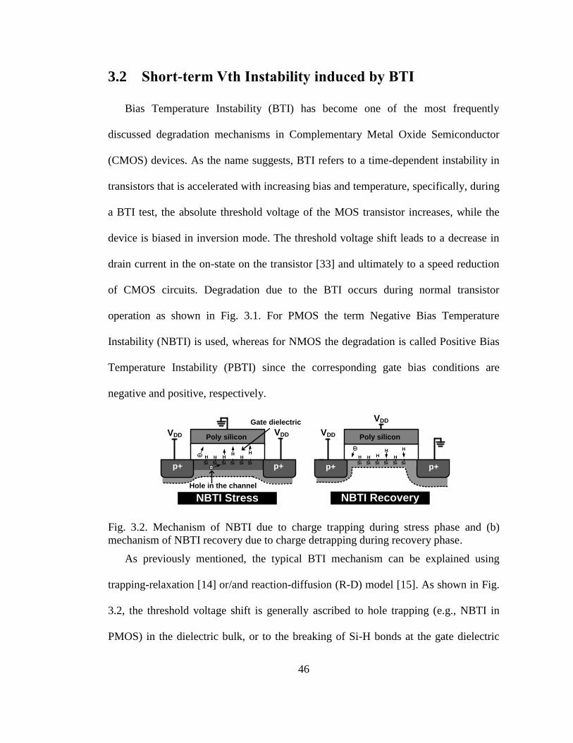
46
3.2 Short-term Vth Instability induced by BTI
Bias Temperature Instability (BTI) has become one of the most frequently
discussed degradation mechanisms in Complementary Metal Oxide Semiconductor
(CMOS) devices. As the name suggests, BTI refers to a time-dependent instability in
transistors that is accelerated with increasing bias and temperature, specifically, during
a BTI test, the absolute threshold voltage of the MOS transistor increases, while the
device is biased in inversion mode. The threshold voltage shift leads to a decrease in
drain current in the on-state on the transistor [33] and ultimately to a speed reduction
of CMOS circuits. Degradation due to the BTI occurs during normal transistor
operation as shown in Fig. 3.1. For PMOS the term Negative Bias Temperature
Instability (NBTI) is used, whereas for NMOS the degradation is called Positive Bias
Temperature Instability (PBTI) since the corresponding gate bias conditions are
negative and positive, respectively.
p+ p+Si
Hole in the channel
H
Si
H
Si
H
Gate dielectric
Si
H
Si Si
H
p+ p+Si
H
Si
H
Si
H
Si
H
Si
H
Si
H
NBTI Stress NBTI Recovery
H
+
+
+
VDD
VDDVDDVDD Poly silicon Poly silicon
Fig. 3.2. Mechanism of NBTI due to charge trapping during stress phase and (b)
mechanism of NBTI recovery due to charge detrapping during recovery phase.
As previously mentioned, the typical BTI mechanism can be explained using
trapping-relaxation [14] or/and reaction-diffusion (R-D) model [15]. As shown in Fig.
3.2, the threshold voltage shift is generally ascribed to hole trapping (e.g., NBTI in
PMOS) in the dielectric bulk, or to the breaking of Si-H bonds at the gate dielectric

47
interface by holes in the inversion layer, which generates positively charged interface
traps (e.g., NBTI in PMOS). When a stressed device is turned off, it enters the
“recovery” phase immediately, where trapped holes are released, or the freed
hydrogen species diffuse back towards the dielectric interface to anneal the broken Si-
H bonds, thereby reducing the threshold voltage shift. For conventional poly-Si
electrodes, BTI is typically only observed in PMOS transistors since the electron
trapping in SiO2 is small, but the introduction of high-k (HK) dielectrics into the
CMOS manufacturing process recently, both PMOS and NMOS transistors are now
exhibiting BTI [34, 35]. This is because that the negative charge trapping in the HK
layer or in the region between the HK layer and the interfacial oxide layer during
PBTI in HK metal gate NMOS transistors has been mainly observed. Both NBTI and
PBTI exhibit the strong voltage and temperature dependences. Based on the traditional
R-D model and superposition assumption, the stress-relaxation (recovery) model [36]
can be expressed as shown in Fig. 3.3. The stress and recovery characteristics of BTI-
induced short-term Vth shifts play an important role during the operation of CMOS
digital and analog circuits in conventional poly-Si and HK metal gate processes.
Fig. 3.3. BTI stress and relaxation (recovery) models [36] based on R-D model and
superposition assumption. Here, 𝑛 is the stress time exponent, α is the voltage
acceleration factor, 𝐸𝑎 is the thermal activation energy, 𝑘 is the Boltzmann constant,
and 𝑇 is the absolute temperature.

48
3.3 Impact of Short-term Vth Instability on SAR ADC
operation
In most analog circuits (e.g., amplifiers, bias generators), the gate-to-source and
drain-to-source voltages are typically lower than the supply voltage, so the absolute
value of Vth degradation and recovery induced by BTI is inherently small compared to
that of digital logic. However, in a comparator used in differential SAR ADCs, the two
input transistors of a comparator may be subject to an asymmetric voltage stress
during the initial SAR conversion steps as shown in Fig. 3.4, giving rise to a relatively
large difference in their short-term Vth shifts. This may lead to an incorrect decision
by the comparator especially during the second or third SAR conversion steps, which
cannot be corrected by the subsequent conversion steps.
The example in Fig. 3.4 shows an incorrect conversion in the second SAR
conversion step D8 when the input voltage difference (C) is smaller than Vth shift
difference (B) caused by the large input voltage difference (A) applied during the
preceding D9 step. In theory, an incorrect decision can occur during any SAR
conversion step, from D8 to D0. However, the likelihood of an error is higher for the
earlier steps since the input transistors are subject to a larger voltage difference in
these steps.
To give a quantitative example, let us consider a 100kS/s 10-bit differential SAR
ADC with a 1.2V supply voltage. Each conversion step takes 1/100k/10bits = 1µs to
complete. Since one LSB corresponds to 1.2V/210 = 1.17mV, any short-term Vth shift
difference greater than this voltage can cause an incorrect comparator decision. Using
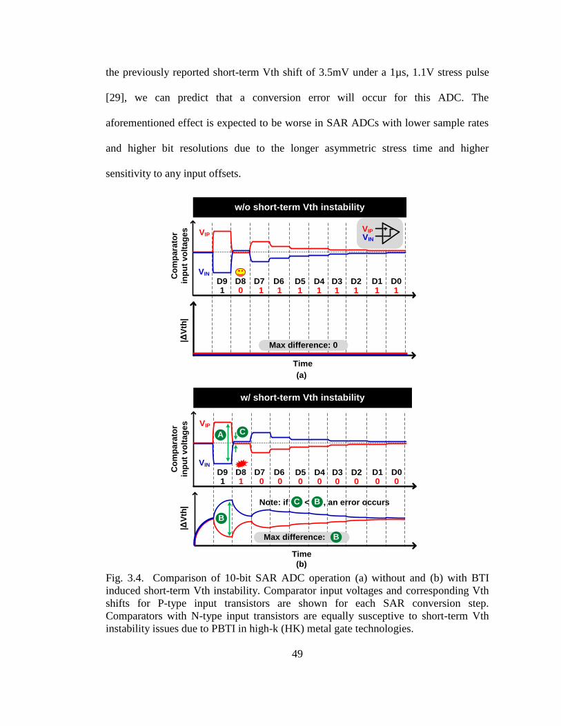
49
the previously reported short-term Vth shift of 3.5mV under a 1µs, 1.1V stress pulse
[29], we can predict that a conversion error will occur for this ADC. The
aforementioned effect is expected to be worse in SAR ADCs with lower sample rates
and higher bit resolutions due to the longer asymmetric stress time and higher
sensitivity to any input offsets.
1 0 1 1 1 1
VIP
VIN
D9 D8 D7 D6 D1 D0
|ΔV
th|
w/o short-term Vth instability
w/ short-term Vth instability
Note: if < , an error occurs
Time
Co
mp
ara
tor
inp
ut
vo
lta
ge
s
C
C B
1 1D3 D2
1 1D5 D4
Max difference: 0
1 1 0 0 0 0
VIP
VIN
D9 D8 D7 D6 D1 D00 0
D3 D20 0
D5 D4
B
Max difference: BBB
VIP
VIN
A
Time
(a)
(b)
|ΔV
th|
Co
mp
ara
tor
inp
ut
vo
lta
ge
s
Fig. 3.4. Comparison of 10-bit SAR ADC operation (a) without and (b) with BTI
induced short-term Vth instability. Comparator input voltages and corresponding Vth
shifts for P-type input transistors are shown for each SAR conversion step.
Comparators with N-type input transistors are equally susceptive to short-term Vth
instability issues due to PBTI in high-k (HK) metal gate technologies.

50
3.4 Proposed Stress Equalization and Stress Removal
Techniques
We propose two techniques [37] for mitigating the aforementioned effect. Fig. 3.5
illustrates the basic idea compared to a typical SAR ADC operation.
Difference: BB
D9
Recovery
(input transistors OFF)
D8
D9
Equalization
D8
lΔV
thl
VIP
D9
t
D8
Typical SAR
Stress removal
Stress equalization
t
t
VIP
VIN
VIP
If < , an error occurs
No error occurs
No error occurs
Co
mp
. in
pu
t v
olt
ag
es
YX
t
t
t
X
Y
VIN
VIN
VDD
0.5
VDD
Stress
Stress
Stress
(a)
(b)
(c)
lΔV
thl
Co
mp
. in
pu
t v
olt
ag
es
VDD
0.5
VDD
lΔV
thl
Co
mp
. in
pu
t v
olt
ag
es
VDD
0.5
VDD
Fig. 3.5. Illustration of proposed (b) stress equalization and (c) stress removal
techniques compare to (a) a typical SAR ADC [37]. Comparator input voltages and
corresponding Vth shift are shown for just the first D9 conversion step here for
simplicity.

51
By equalizing the input voltages to the common mode voltage VDD/2 (namely stress
equalization), or by connecting them to VDD (namely stress removal) right after the
conversion, the comparator input offset Y due to the asymmetric voltage stress can be
recovered (or minimized) prior to the next conversion step. Note that we chose VDD/2
as the equalization voltage since the common mode voltage for a rail-to-rail input
signal is VDD/2. It ensures same setting time for reaching VDD/2 on both comparator
inputs. The proposed techniques are highly effective in enhancing the performance of
low sample rate SAR ADCs since the techniques can provide a long recovery time.

52
3.5 Circuit Implementations in 65nm CMOS
The proposed stress equalization and stress removal techniques are demonstrated
on a 10-bit differential charge-redistribution SAR ADC consisting of the new
comparator, binary-weighted capacitor arrays, and successive approximation registers
as shown in Fig. 3.6. To suppress the substrate and supply noise, and to ensure good
common-mode rejection, a fully differential architecture is employed in the proposed
SAR ADC.
VREF
VIN
VCM
VIP
VREF
Comparator with
proposed techniques
SAR
Controller
D0
~ D
9
10b
CLK
51
2C
25
6C
12
8C
64
C
32
C
16C
8C
4C
2C
1C
1C
C_CLK
51
2C
25
6C
12
8C
64
C
32
C
16C
8C
4C
2C
1C
1C
Fig. 3.6. Block diagram of a 10-bit differential charge-redistribution SAR ADC. The
proposed stress mitigation techniques are implemented in the comparator circuit block.
3.5.1 Successive Approximation Register
The basic structure [38] of the 10-bit SAR is a multiple input shift register, as
shown in Fig. 3.7. The internal structure of each multiple input shift register and the
associated truth table are shown in Fig. 3.8. It consists of a positive-edge triggered D
flip-flop (DFF), a decoder, and a multiplexer. By adding a multiplexer and a decoder
to each DFF, the three different inputs can be selected according to the truth table in
Fig. 3.8. Whenever the DFFs are triggered, the kth DFF will have three different data

53
inputs coming from: (1) the output of the (k+1)th DFF (shift right), (2) the output of
the PC, Comp (data load), and (3) the outputs of the kth DFF itself (memorization).
Details of the operating sequence can be found in [38].
Fig. 3.7. 10-bit SAR logic circuit [38]
Fig. 3.8. Internal structure of the kth flip-flop [38]

54
3.5.2 Binary-weighted Capacitor Arrays
For the binary-weighted capacitor arrays, the Metal-Insulator-Metal (MIM)
capacitors are used. A unit capacitor consists of five metal layers and the capacitance
of a unit capacitor (3 μm x 4 μm) is about 10.8 fF. The binary-weighted capacitor
array of the implemented 10-bit SAR ADC uses 29 unit capacitors. Therefore, the total
sampling capacitance of one capacitor network is 5.53 pF. The two capacitor networks
occupy a total active area of 430 μm x 320 μm, about 62% of the whole ADC. Due to
the small unit capacitance, the routing parasitic capacitance has a considerable
influence on the ratio of capacitances. The capacitors were placed in an intuitive way
to simplify the layout routing [39]. Fig. 3.9 shows the layout floorplan of the capacitor
array.
Fig. 3.9. The layout floorplan of the capacitor array [39].

55
3.5.3 Comparator with the proposed techniques
The comparator with the proposed techniques shown in Fig. 3.10, consists of a
preamp, a latch, and a logic circuit with a feedback loop. The logic circuit controls the
comparator input nodes by connecting them to either the recovery or equalization
voltages VDD or VDD/2, right after the comparator makes a decision, and returning to
the original input voltages VIN and VIP just prior to the next SAR conversion step.
This specific sequence ensures that the comparator input offset due to asymmetric
voltage stress is minimized without interfering with the original SAR operation.
A preamp stage is used in the SAR comparator to suppress the input-referred noise
of the subsequent latch stage. Although both NMOS and PMOS type input transistors
can be considered in the preamp as previously explained in Chapter 3.2, we chose the
latter option as PMOS NBTI is more dominant than NMOS PBTI in the 65nm process
used for this study. An added benefit of using PMOS input transistor is the reduced 1/f
noise [31]. Note that NMOS input transistors will be equally affected by PBTI in high-
k metal gate technologies and hence the short-term Vth shift effect will occur
regardless of the input transistor type in more advance nodes [32].
Fig. 3.10 (bottom) shows the simplified timing diagram of the proposed technique.
When the comparator clock COMP_CLK is low, the two outputs of the latch VON and
VOP are pre-discharged. The comparator evaluates on the rising edge of COMP_CLK
and subsequently one of the two outputs will go high. A NOR gate detects this low-to-
high transition and asserts a decision-complete-indication signal DONEb. A NAND
gate with inputs C_CLK and DONEb generates a gate-control-signal GATE_CTRL to
control the comparator input nodes. To ensure that the proposed techniques do not

56
interfere with the original SAR operation, an additional delay tD is inserted between
the C_CLK and the COMP_CLK.
VIP VIN
GATE_CTRLGATE_CTRL
VDD or
VDD/2
VDD or
VDD/2
COMP
_CLKb
VOPVON
VBp
VBn
COMP_CLK
VON, VOP
DONEb
C_CLK
COMP_CLKb
VOP
VONGATE_CTRL
Stress equalization
or stress removal
DONEb
COMP
_CLKb
GATE_CTRL
Delay (tD)
COMP_CLK
C_CLK
tD tD
(a)
(b)
Fig. 3.10. (a) Schematic and (b) timing diagrams of comparator circuit consisting of a
pre-amp stage and a latch circuit [31]. Additional switches are used for the proposed
stress equalization and stress removal techniques.

57
3.6 SAR ADC Test-chip Measurement Results
A 10-bit differential SAR ADC employing the two proposed techniques was
implemented in a 65nm test-chip. The sampling frequency of 80kS/s was used for the
experiments. Fig. 3.11 shows the measured DNL and INL for the proposed and
conventional SAR ADC design. The DNL is improved by 0.90 LSB and 0.77 LSB for
the stress equalization and stress removal techniques, respectively, while INL data
showed no apparent advantage. The DNL plots also reveal that the actual
improvement in DNL depends on the digital output code and that there are particular
digital outputs, namely points A~F in Fig. 3.11, which show a large improvement in
DNL. A careful inspection of these digital outputs, also summarized in Fig. 3.12,
reveals that these are the output codes wherein an error occurs in the initial conversion
steps. That is, a conversion error occurred in the D8 or D7 conversion steps which
agrees with our hypothesis in Fig. 3.4. The relatively large asymmetric voltage stress
applied during the first couple of steps (i.e. D9 or D8) are primarily responsible for the
errors caused by device instability issues. A 65536-point FFT of a sinusoidal input
with a frequency of 2.205kHz sampled at 80kS/s is shown in Fig. 3.13. Subtle
improvements in SNDR, ENOB, and SFDR can be observed. The die photo and
performance summary of the implemented SAR ADC are shown in Fig. 3.14. The
active circuit area is 450x490μm2 and the ADC employing the proposed stress
mitigation techniques achieves a worst case DNL of -0.46/+1.03 LSB, worst case INL
of -1.21/+1.22 LSB, SNDR of 50.79dB (or ENOB of 8.14), and an SFDR of 65.65dB.

58
Typical SAR
-1
-0.5
0
0.5
1
DN
L (
LS
B) 1.5
2
-1.5
-1
0
-0.5
1
INL
(L
SB
)
0 256 512 768 1024
1.5
0.5
0 256 512 768 1024
0 256 512 768 1024
Stress removal
Stress equalization
DNLMAX = -0.46 / +1.93
DNLMAX = -0.45 / +1.16
INLMAX = -1.24 / +1.23
DNLMAX = -0.46 / +1.03
INLMAX = -1.21 / +1.22
INLMAX = -1.22 / +1.21
0.77
0.90
A B C DE F
Digital Out
Digital Out
Digital Out
-1
-0.5
0
0.5
1
DN
L (
LS
B) 1.5
2
-1.5
-1
0
-0.5
1
INL
(L
SB
)
1.5
0.5
-1
-0.5
0
0.5
1
DN
L (
LS
B) 1.5
2
-1.5
0
-0.5
1
INL
(L
SB
)
1.5
0.5
(a)
(b)
(c)
Fig. 3.11. Measured DNL (top) and INL (bottom) using (b, c) the proposed techniques
compared to (a) a typical SAR ADC. Measured data from a 65nm test-chip shows a
DNL improvement of 0.90 and 0.77 LSB using stress equalization and stress removal,
respectively. The impact on INL was negligible.
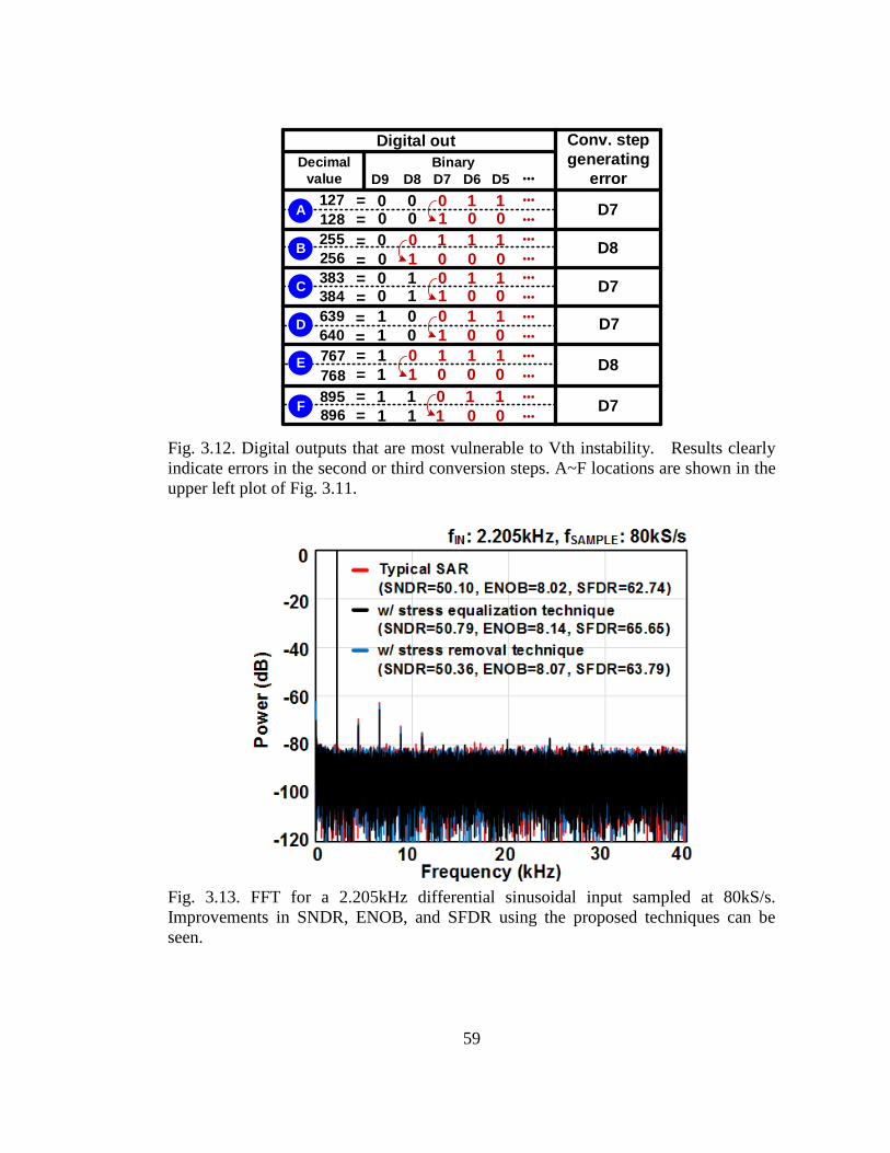
59
895
D9
639
383
255
127
767
Decimal
value
Digital out
D8 D7 D6 D5
1 1 0 1
1 0 1 1
1 0 0 1
0 1 0 1 1
0 0 1 1 1
0 0 0 1 1
1 1 1 0 0
1896
1
1 1 0 00768
640 1 0 1 0 0
1
384 0 1 1 0 0
256 0 1 0 0 0
128 0 0 1 0 0
=
=
=
=
=
=
=
=
=
=
=
=A
B
C
D
E
F
Conv. step
generating
error
D7
D8
D7
D7
D8
D7
Binary
Fig. 3.12. Digital outputs that are most vulnerable to Vth instability. Results clearly
indicate errors in the second or third conversion steps. A~F locations are shown in the
upper left plot of Fig. 3.11.
Fig. 3.13. FFT for a 2.205kHz differential sinusoidal input sampled at 80kS/s.
Improvements in SNDR, ENOB, and SFDR using the proposed techniques can be
seen.
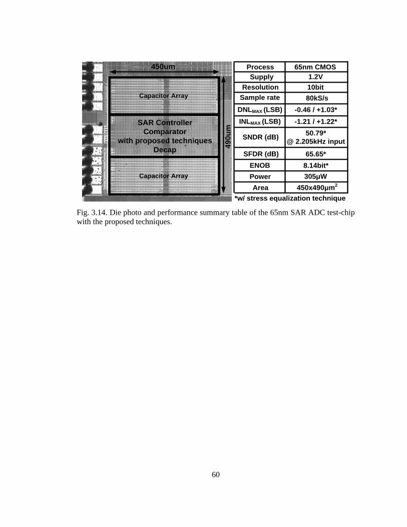
60
Process 65nm CMOS
Supply 1.2V
80kS/s
Power 305μW
Resolution
Sample rate
8.14bit*ENOB
10bit
450x490μm2
Area
50.79*
@ 2.205kHz inputSNDR (dB)
49
0u
m
450um
Capacitor Array
Capacitor Array
SAR Controller
Comparator
with proposed techniques
Decap
-0.46 / +1.03*DNLMAX (LSB)
-1.21 / +1.22*INLMAX (LSB)
*w/ stress equalization technique
65.65*SFDR (dB)
Fig. 3.14. Die photo and performance summary table of the 65nm SAR ADC test-chip
with the proposed techniques.

61
3.7 Conclusion
In this Chapter, we present two circuit techniques for mitigating short-term Vth
instability issues in SAR ADCs. The proposed techniques temporarily connect the
comparator input nodes to the same voltage level right after each conversion is
complete. This either equalizes or eliminates the short-term Vth instability of the input
transistors, thereby preventing incorrect decision from being made by the comparator
circuit. Measured data from a 65nm 10-bit SAR ADC test-chip shows that the
proposed techniques reduce the worst case DNL by 0.90 LSB using stress equalization,
and by 0.77 LSB using stress removal, compared to a conventional SAR ADC.

62
Chapter 4. Spintronics-based Mixed-signal
Circuits: TRNG, ADC, and Temperature Sensor
This chapter proposes new classes of TRNG, ADC, and temperature sensor based
on the random switching behavior of a Magnetic Tunnel Junction (MTJ) which are
experimentally demonstrated for the first time. This work aims at leveraging and
complimenting on-going development efforts in MTJ technology for non-memory
mixed-signal applications. The proposed MTJ based TRNG, ADC, and temperature
sensor have the potential to achieve a compact area, simpler design, and reliable
operation as compared to their CMOS counterparts.
4.1 Introduction
A True Random Number Generators (TRNGs), Analog-to-digital converters
(ADCs), and on-chip temperature sensors are specialized building blocks used
extensively in hardware-based security, sensing applications, and thermal management
of multi-core microprocessors, respectively.
Fig. 4.1 illustrates a cryptography system as an example application where the true
random number generators are used for generating random numbers. In the system, on
the transformation of data in encryption and decryption process, random numbers are
used to generate the secret keys. For generating these random numbers, true random
number generators have been recently investigated and have begun to replace pseudo
random number generators. This is because the true random number generators can
generate independent, unpredictable, nondeterministic, and aperiodic random numbers
so that they ensure a high level of security in the cryptography and security systems.

63
Traditional CMOS based TRNGs utilize physical noise present in CMOS circuits
such as thermal noise, random telegraph noise, and oscillator jitter. However, existing
CMOS based TRNGs require extensive post-processing to ensure a high level of
randomness in the output bits, which incurs a significant performance, power, and area
overhead [40].
Fig. 4.1. A cryptography system as an application of True Random Number Generator
(TRNG).
Analog-to-Digital Converters are universally used in everywhere to interact
between analog world and digital systems as shown in Fig. 4.2. An N-bit ADC
samples a continuous analog signal, quantizes it into 2N discrete levels, and finally,
converts to digital output codes at discrete time intervals. Significant research progress
has been made towards improving the ADC’s energy-efficiency, resolution, and
sampling speed in advanced CMOS technologies [41]. Traditional CMOS based
ADCs can be classified into several different architectures: namely, successive
approximation, flash, sigma-delta, pipelined, and time-interleaved. However, meeting

64
the demand of today’s electronic systems in the face of aggressive transistor scaling
has proven to be a challenge as designers have to grapple with device level issues such
as process variation, threshold voltage instability, noise, and limited voltage headroom.
VIN DOUT
time
An
alo
g
Am
plitu
de
time
Dig
ita
l
Va
lue
Resolution: N bits
(=2N quantization steps)
Analog Digital
Fig. 4.2. Operating principle of an Analog-to-Digital Converter (ADC).
The on-chip temperature sensors are embedded at multiple locations in a
microprocessor and monitor temperatures that are used to manage the operation of the
microprocessor under local and global thermal constraints. While existing sensors
achieve impressive area and accuracy, emerging technology trends such as multi-core
architectures, 3D integration, and low-voltage operation demand even better sensors
with difficult-to-meet requirements. Those requirements are three-fold [56]: 1)
Sensors need to be area efficient. By increasing the number of cores and hot spots,
there are more locations that require thermal monitoring. To reduce the overhead, the
sensor footprint needs to be minimized. 2) Sensors need to have low calibration cost,
while achieving sufficient accuracy. The requirements of <8°C in absolute inaccuracy
and <3°C in relative inaccuracy have been outlined in [55]. 3) Finally, the sensors

65
need better supply voltage (VDD) scalability. Sub- 1V operation for digital systems is
being explored to reduce power. The conventional CMOS based temperature sensors
often cannot operate below 1V, necessitating additional power distribution or
regulation.
The goal of this work is to develop new classes of TRNG, ADC, and temperature
sensor based on the random switching behavior of a Magnetic Tunnel Junction (MTJ)
for compact area, simpler design, and reliable operation. MTJ technology has matured
to the point where commercial STT-MRAM chips are currently being developed. This
work aims at leveraging and complimenting on-going development efforts in MTJ
technology for non-memory mixed-signal applications. For the TRNG demonstration,
we propose a conditional perturb and real-time output probability tracking scheme to
achieve a 100% bit efficiency (or 100% useable bits) while improving the reliability,
speed, and power consumption. For the ADC demonstration, two circuit techniques
were implemented to improve the ADC linearity and increase the input voltage range.
The proposed ADC achieves an 8-bit resolution with excellent linearity at 30 and
85°C. For showing the feasibility of temperature sensor, an MTJ in the thermal
activated switching regime was used to show the temperature dependence of the
switching probability. Our experiment data show that the switching probability with a
pulse width of 500ns exhibits good linearity in temperature range between 30 and
90°C with a slope (i.e., temperature coefficient) of 0.51 [%/°C]. The worst-case
temperature error with 2-temperature point calibration is less than +0.60 / -0.91°C.
The remainder of this chapter is organized as follows. Section 4.2 provides the
introduction of MTJ. Section 4.3 describes the operating principle of the proposed

66
MTJ-based TRNG. In addition, the details of the proposed conditional perturb and
real-time output probability tracking schemes are shown. Section 4.4 proposes the
MTJ-based ADC with circuit techniques for improving linearity and input voltage
range. Section 4.5 shows the feasibility of the MTJ-based temperature sensor with the
promising experiment data, and Section 4.6 concludes the chapter.

67
4.2 Magnetic Tunnel Junction (MTJ)
We first give a brief introduction to MTJ for context. The MTJ is a storage device
which is widely used in Spin-transfer-torque magnetic RAMs (STT-MRAMs). As
shown in Fig. 4.3(a), the MTJ consists of two ferromagnetic (FM) layers, a free layer
and a pinned layer, separated by a thin insulating tunneling barrier. The MTJ
resistance is determined by the relative magnetization orientations of two FM layers,
i.e. parallel state (RP, low resistance) and anti-parallel state (RAP, high resistance).
From a circuit perspective, the MTJ can be considered as a voltage controlled variable
resistance, which can be represented by the resistance-voltage (R-V) hysteresis curve
shown in Fig. 4.3(b). Depending on the direction of switching current, spin-polarized
electrons exert spin torque to the free layer and induce the magnetization switching in
the preferred direction as shown in Fig. 4.4 [50].
Magnetic anisotropy decides the energetic preference of the magnetization
direction often referred to as the easy axis. Depending on the source of the anisotropy,
the MTJs can be classified into the following three categories: shape anisotropy-based
in-plane MTJ (IMTJ), crystal anisotropy-based perpendicular MTJ (C-PMTJ), and
interface anisotropy-based perpendicular MTJ (I-PMTJ). IMTJ technology is far more
mature than their perpendicular counterparts, however there is growing interest in the
perpendicular devices as they are believed to have a low switching current density. In
our demonstrations, a shape anisotropy-based in-plane MTJ device was used but, other
MTJ types can be considered in future demonstrations.

68
We can define the tunneling magnetoresistance (TMR) as the ratio between the
resistances of the two states. A higher TMR is preferred for a reliable read operation
of MTJ state as it will generate a larger signal difference between the two states. The
physics and dependency of TMR on MTJ processing parameters can be found in [51].
Another critical parameter is the thermal stability factor (Δ) which is the energy
barrier between the parallel and anti-parallel states normalized to the thermal
fluctuation energy. The probability of thermally assisted switching depends on the Δ
which determines the level of non-volatility of the free layer. Δ can be expressed as
Δ = Eb / (kB ∙ T) = (Ku ∙ V) / (kB ∙ T) (1)
where Eb is the energy barrier between two states, kB is the Boltzmann constant, T is
the absolute temperature, Ku is the uniaxial magnetic anisotropy energy density, and V
is the volume of the magnet [52].
Fig. 4.3. (a) Magnetic tunnel junction (MTJ) stack and its equivalent circuit model, a
two-terminal device with variable resistance. (b) Typical R-V hysteresis curve of an
MTJ.

69
IC_AP-P
e-
AP-P
switching
IC_P-AP
e-
P-AP
switching
Anti-parallel: High R
Anti-parallel: High R
Parallel: Low R
Parallel: Low R
Free layerTunnel barrierPinned layer
Free layerTunnel barrierPinned layer
Fig. 4.4. Illustration of Spin Transfer Torque (STT) switching principle in an MTJ.

70
4.3 MTJ-based True Random Number Generator
4.3.1 Operating Principle, Experiment Setup, and Design Considerations
The Spin Transfer Torque (STT) switching phenomenon in an MTJ is subject to
random thermal fluctuation noise which gives rise to a switching probability contour
map as shown in Fig. 4.5 [42]. By applying an optimal “perturb” pulse whose width
and amplitude correspond to the 50% switching probability contour, the final resolved
state of the MTJ will depend solely on the random thermal noise, producing an
unbiased random output bit. In this work, we address the two main considerations for
a high quality TRNG design: (1) achieving the optimal trade-off between switching
speed, power, and lifetime, and (2) ensuring a 50% switching probability under
different PVT conditions.
Switching
probability
(%)
(+) Switching speed
( ) Switching energy
( ) MTJ lifetime
(+) MTJ lifetime
(+) Switching energy
( ) Switching speed
10090
8070
60
50403020100
Pulse amplitude (V)
0.4 0.5 0.6 0.7 0.8 0.9 1.0
Pu
lse
wid
th (
ns
)
1
2
3
4
5
6
7
8
9
10
50% contour
Fig. 4.5. MTJ switching probability as a function of pulse width and pulse amplitude
[42] (APP switching direction).

71
4.3.2 Proposed Conditional Perturb Scheme
The working principles of the conventional unconditional reset scheme [44]
(concept only) and the proposed conditional perturb scheme are described in Fig. 4.6.
The conventional technique applies an initial reset voltage (VRESET) large enough to
force the MTJ into a reset state (i.e. AP). Subsequently, a smaller perturbation voltage
VPERTURB+ in the opposite direction (i.e. AP to P) is applied to induce STT
switching with a 50% probability. Finally, the resolved state is read out using a small
read voltage (VREAD). The proposed scheme in [53], on the other hand, perturbs the
cell according to the previously sampled MTJ state, thereby eliminating the reset
phase all together.
V
VPERTURB+
VRESET
0
One cycle
RepeatV
0
Repeat
One cycle
OR
tRESET tREAD
tPERTURBtREAD
VPERTURB+
VPERTURB-
1. Reset 2. Perturb
3. Read resolved state
Time Time
tPERTURB
1. Read resolved state
2. Conditional perturb
Unconditional reset scheme
([44], no measured data)
Proposed conditional
perturb scheme
OR
OR
Fig. 4.6. Random number generation schemes: (left) unconditional reset scheme [44]
and (right) the proposed conditional perturb scheme [53].

72
1X (Slow)
1bit / (tRESET+tPERTURB+tREAD) Bit rate
1.67X (Fast)
1bit / (tREAD+tPERTURB)
Switching
energy1X (High)
ERESET+EPERTURB+EREAD
0.29X (Low)
EREAD+EPERTURB
Design
overheadStrong reset driver
Polarity detection,
symmetric APP and
PAP switching
MTJ
lifetime
Short time-to-
breakdown
Long time-to-
breakdown
Unconditional
reset scheme
([44], no measured data)
Proposed conditional
perturb scheme
Fig. 4.7. TRNG performance comparison between the unconditional reset and the
proposed conditional perturb schemes.
V
0.5V
-0.8V
0
One cycle
RepeatV
0
Repeat
One cycle
OR
Unconditional reset Conditional perturb
3ns 3ns
3ns3ns
0.5V
-0.5V
Time Time
3ns
0.1V 0.1V
(a)
(b)
100
103
106
109
1012
1015
1018
1021
Effective Time to Breakdown (sec)
0.01
0.09
0.67
4.85
30.77
93.40
Fa
ilu
re (
%)
8.3E+24 bits
generated
5.5E+16 bits
generated
Unconditional
reset
Conditional
perturb
Fig. 4.8. (a) Timing diagrams for MTJ Time-to-breakdown (tBD) analysis (b) Lifetime
comparison between the two TRNG schemes based on MTJ measurement data [45,
46].
Fig. 4.7 shows a high level comparison between the two schemes. The advantages
of the proposed technique are threefold. First, the absence of a reset phase enhances
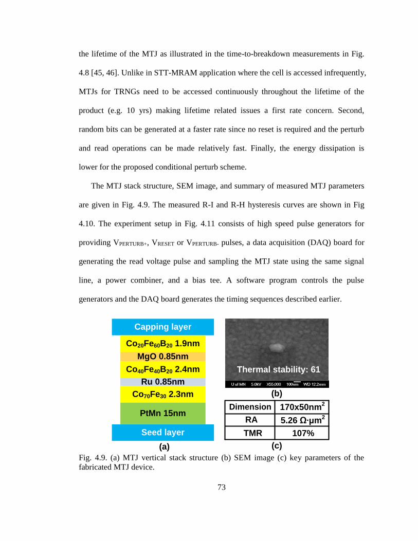
73
the lifetime of the MTJ as illustrated in the time-to-breakdown measurements in Fig.
4.8 [45, 46]. Unlike in STT-MRAM application where the cell is accessed infrequently,
MTJs for TRNGs need to be accessed continuously throughout the lifetime of the
product (e.g. 10 yrs) making lifetime related issues a first rate concern. Second,
random bits can be generated at a faster rate since no reset is required and the perturb
and read operations can be made relatively fast. Finally, the energy dissipation is
lower for the proposed conditional perturb scheme.
The MTJ stack structure, SEM image, and summary of measured MTJ parameters
are given in Fig. 4.9. The measured R-I and R-H hysteresis curves are shown in Fig
4.10. The experiment setup in Fig. 4.11 consists of high speed pulse generators for
providing VPERTURB+, VRESET or VPERTURB- pulses, a data acquisition (DAQ) board for
generating the read voltage pulse and sampling the MTJ state using the same signal
line, a power combiner, and a bias tee. A software program controls the pulse
generators and the DAQ board generates the timing sequences described earlier.
MgO 0.85nm
Capping layer
Co20Fe60B20 1.9nm
Co40Fe40B20 2.4nm
Ru 0.85nm
Co70Fe30 2.3nm
PtMn 15nm
Seed layer
Dimension 170x50nm2
RA
TMR 107%
5.26 Ω∙μm2
(a)
(b)
(c)
Thermal stability: 61
Fig. 4.9. (a) MTJ vertical stack structure (b) SEM image (c) key parameters of the
fabricated MTJ device.

74
400
600
800
1000
1200
1400
-400 0 400H (Oe)
RAP
TMR :
107%
RM
TJ (Ω
)
RP
(a) (b)
400
600
800
1000
1200
1400
-0.4 -0.2 0 0.2 0.4
RM
TJ (Ω
)
IMTJ (mA)
RAP
RP
Fig. 4.10. Measured (a) R-I and (b) R-H hysteresis curves of the fabricated MTJ
device. Data was collected while sweeping (a) the MTJ current (b) and external field.
Pulse Generator 1
(Picosecond 10,070A)
Pulse Generator 2
(*HP 8110A or
**Picosecond 10,060A)
Power
Combiner
(Picosecond
5331-104)
Bias-Tee
(Picosecond
5542-229)
MTJ
DAQ Board
(NI-PCI-6251)
La
bV
iew
TM
Inte
rfa
ce
ADC
Resistance
Random
Number
*For conventional
**For proposed scheme
*Reset or **-Perturb
+Perturb
Read10kOhm
Fig. 4.11. Random number generator measurement setup with sub-50 picosecond
pulse width resolution.
Fig. 4.12 shows the measured probability of each 10.6 Kbit segment for the
conventional conditional reset scheme. Note that the output probability typically needs
to stay within 50±1% to pass the NIST frequency test [47]. A small number of
segments fail to meet this criterion and consequently, the output data fails to pass the
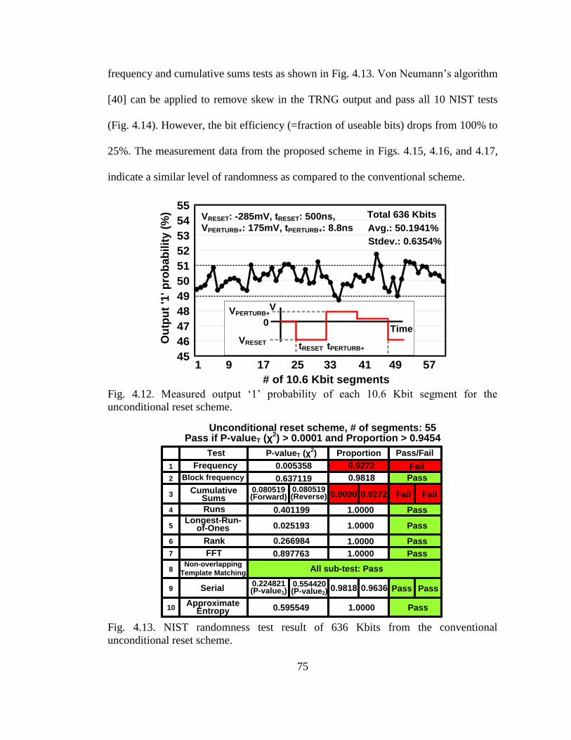
75
frequency and cumulative sums tests as shown in Fig. 4.13. Von Neumann’s algorithm
[40] can be applied to remove skew in the TRNG output and pass all 10 NIST tests
(Fig. 4.14). However, the bit efficiency (=fraction of useable bits) drops from 100% to
25%. The measurement data from the proposed scheme in Figs. 4.15, 4.16, and 4.17,
indicate a similar level of randomness as compared to the conventional scheme.
45
46
47
48
49
50
51
52
53
54
55
1 9 17 25 33 41 49 57
Ou
tpu
t '1
' p
rob
ab
ilit
y (
%)
# of 10.6 Kbit segments
VRESET: -285mV, tRESET: 500ns,
VPERTURB+: 175mV, tPERTURB+: 8.8ns
Total 636 Kbits
Avg.: 50.1941%
Stdev.: 0.6354%
VVPERTURB+
VRESET
0
tRESET
Time
tPERTURB+
Fig. 4.12. Measured output ‘1’ probability of each 10.6 Kbit segment for the
unconditional reset scheme.
Test P-valueT (χ2) Proportion Pass/Fail
1 Frequency 0.005358 0.9272 Fail
2 Block frequency 0.637119 0.9818 Pass
3Cumulative
Sums0.080519 (Forward)
0.080519(Reverse) 0.9090 0.9272 Fail Fail
4 Runs 0.401199 1.0000 Pass
5Longest-Run-
of-Ones 0.025193 1.0000 Pass
6 Rank 0.266984 1.0000 Pass
7 FFT 0.897763 1.0000 Pass
8Non-overlapping
Template MatchingAll sub-test: Pass
9 Serial0.224821 (P-value1)
0.554420 (P-value2)
0.9818 0.9636 Pass Pass
10Approximate
Entropy 0.595549 1.0000 Pass
Pass if P-valueT (χ2) > 0.0001 and Proportion > 0.9454
Unconditional reset scheme, # of segments: 55
Fig. 4.13. NIST randomness test result of 636 Kbits from the conventional
unconditional reset scheme.

76
Test P-valueT (χ2) Proportion Pass/Fail
1 Frequency 0.181557 1.0000 Pass
2 Block frequency 0.062821 1.0000 Pass
3Cumulative
Sums0.554420 (Forward)
0.055361 (Reverse) 1.0000 1.0000 Pass Pass
4 Runs 0.514124 0.9818 Pass
5Longest-Run-
of-Ones 0.145326 1.0000 Pass
6 Rank 0.823537 1.0000 Pass
7 FFT 0.000347 1.0000 Pass
8Non-overlapping
Template MatchingAll sub-test: Pass
9 Serial0.401199 (P-value1)
0.366918 (P-value2)
0.9818 0.9818 Pass Pass
10Approximate
Entropy 0.924076 1.0000 Pass
Pass if P-valueT (χ2) > 0.0001 and Proportion > 0.9454
Unconditional reset scheme, # of segments: 55After Von Neumann Correction
Fig. 4.14. NIST randomness test results for the unconditional reset scheme after
applying the Von Neumann correction (bit efficiency: 25%).
45
46
47
48
49
50
51
52
53
54
55
1 9 17 25 33 41 49 57
# of 10.6 Kbit segments
VPERTURB+: +220mV, tPERTURB+: 9.0ns,
VPERTURB-: -215mV, tPERTURB-: 8.5ns
Total 623 Kbits
Avg.: 50.2037%
Stdev.: 0.6259%
V
0OR
tPERTURB-
VPERTURB+
VPERTURB-Time
tPERTURB+
Ou
tpu
t '1
' p
rob
ab
ilit
y (
%)
Fig. 4.15. Measured output ‘1’ probability of each 10.6 Kbit segment for the proposed
conditional perturb scheme.

77
Test P-valueT (χ2) Proportion Pass/Fail
1 Frequency 0.000831 0.9272 Fail
2 Block frequency 0.266918 0.9464 Pass
3Cumulative
Sums0.037566 (Forward)
0.021999 (Reverse) 0.9272 0.9272 Fail Fail
4 Runs 0.437274 1.0000 Pass
5Longest-Run-
of-Ones 0.474986 0.9818 Pass
6 Rank 0.085953 1.0000 Pass
7 FFT 0.437274 1.0000 Pass
8Non-overlapping
Template MatchingAll sub-test: Pass
9 Serial0.637119 (P-value1)
0.202268(P-value2)
0.9818 0.9818 Pass Pass
10Approximate
Entropy 0.115387 1.0000 Pass
Pass if P-valueT (χ2) > 0.0001 and Proportion > 0.9454
Conditional perturb scheme, # of segments: 55
Fig. 4.16. NIST randomness test result of 623 Kbits from the proposed conditional
perturb scheme.
Test P-valueT (χ2) Proportion Pass/Fail
1 Frequency 0.334538 1.0000 Pass
2 Block frequency 0.637119 1.0000 Pass
3Cumulative
Sums0.249284 (Forward)
0.202268 (Reverse) 1.0000 1.0000 Pass Pass
4 Runs 0.349121 0.9818 Pass
5Longest-Run-
of-Ones 0.200936 1.0000 Pass
6 Rank 0.597670 1.0000 Pass
7 FFT 0.328827 0.9636 Pass
8Non-overlapping
Template MatchingAll sub-test: Pass
9 Serial 0.798139 (P-value1)
0.924076 (P-value2)
1.0000 1.0000 Pass Pass
10Approximate
Entropy 0.080519 0.9636 Pass
Pass if P-valueT (χ2) > 0.0001 and Proportion > 0.9454
Conditional perturb scheme, # of segments: 55After Von Neumann Correction
Fig. 4.17. NIST randomness test results for the conditional perturb scheme after
applying the Von Neumann correction (bit efficiency: 25%).
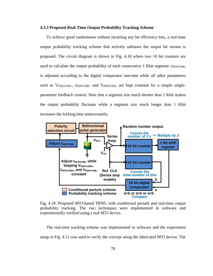
78
4.3.3 Proposed Real-Time Output Probability Tracking Scheme
To achieve good randomness without incurring any bit efficiency loss, a real-time
output probability tracking scheme that actively unbiases the output bit stream is
proposed. The circuit diagram is shown in Fig. 4.18 where two 10 bit counters are
used to calculate the output probability of each consecutive 1 Kbit segment. tPERTURB-
is adjusted according to the digital comparator outcome while all other parameters
such as VPERTURB+, tPERTURB+ and VPERTURB- are kept constant for a simple single-
parameter feedback control. Note that a segment size much shorter than 1 Kbit makes
the output probability fluctuate while a segment size much longer than 1 Kbit
increases the locking time unnecessarily.
Vref
Sense
Amp.
Random number output
10 bit counter
10 bit counter
Adjust tPERTURB-
Ref. CLK
(Sense amp
enable)
1 bit shift
register
10 bit digital
comparatora
a>b or a=b or a<b
Adjust tPERTURB- while
keeping VPERTURB+,
tPERTURB+, and VPERTURB-
constant
Counts the number of 1's Multiply by 2
Compare
Counts the total number of bits
Bidirectional
pulse generator
b
Polarity
selection circuit
Probability tracking schemeConditional perturb scheme
VMTJ
Fig. 4.18. Proposed MTJ-based TRNG with conditional perturb and real-time output
probability tracking. The two techniques were implemented in software and
experimentally verified using a real MTJ device.
The real-time tracking scheme was implemented in software and the experiment
setup in Fig. 4.11 was used to verify the concept using the fabricated MTJ device. The

79
conditional perturb scheme was used for all measurements involving real-time
tracking. Measured probability of each 1 Kbit segment and the corresponding tPERTURB-
are illustrated in Fig. 4.19. The minimum tPERTURB- step was set as 0.05ns. After an
initial locking period of 65 Kbits, the output data passed all NIST randomness tests
while maintaining a 100% bit efficiency (Fig. 4.20). Finally, we show a conceptual
diagram of a TRNG implemented using an existing STT-MRAM array (Fig. 4.21),
which could potentially allow massive generation of random numbers with negligible
circuit overhead.
Pro
ba
bilit
y (
%) VPERTURB+: +220mV, tPERTURB+: 8.0ns,
VPERTURB-: -215mV
-Pe
rtu
rb p
uls
e w
idth
(n
s)
# of 1 Kbit segments1 17 33 49 65 81 97
46474849505152535455
7.57.67.77.87.9
88.18.28.38.48.5
Min. pulse width
step: 0.05ns
Initial locking period
Fig. 4.19. Measured output ‘1’ probability and -perturb pulse width for each 1 Kbit
segment with the proposed real-time output probability tracking scheme.
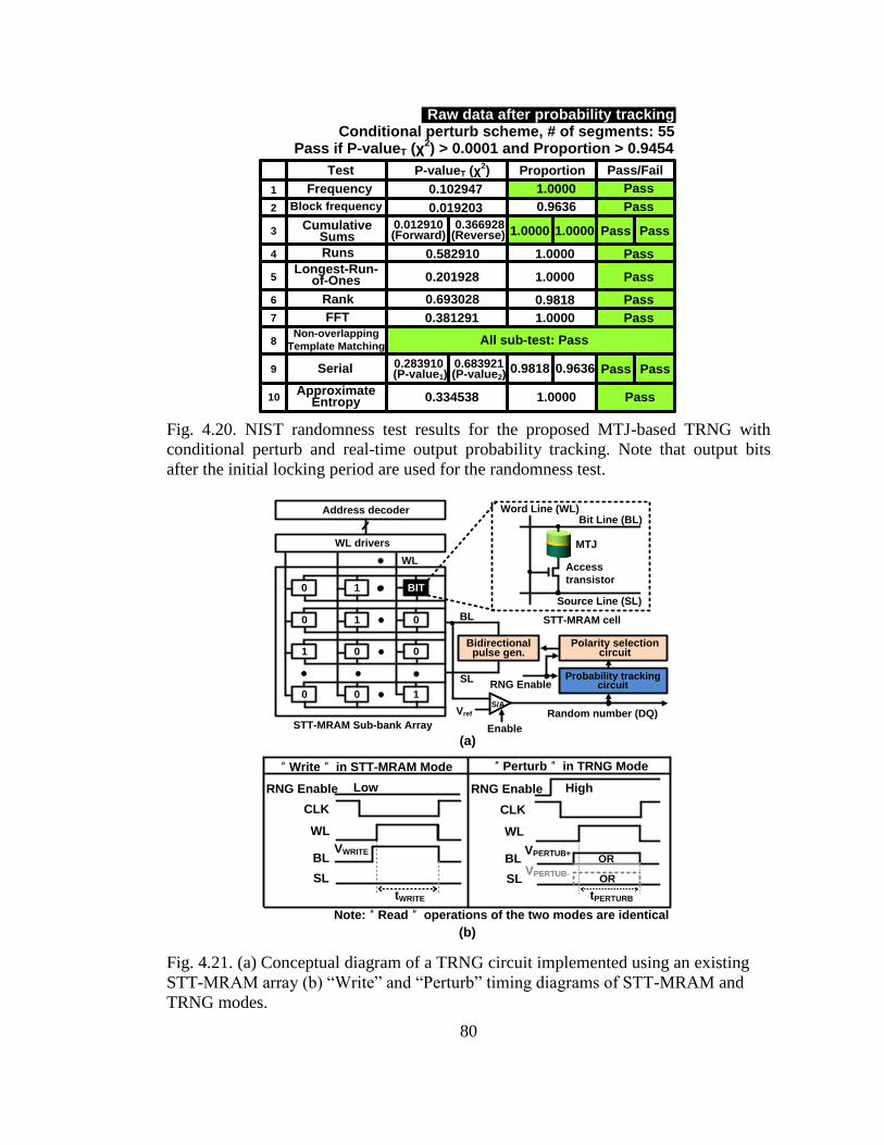
80
Test P-valueT (χ2) Proportion Pass/Fail
1 Frequency 0.102947 1.0000 Pass
2 Block frequency 0.019203 0.9636 Pass
3Cumulative
Sums0.012910 (Forward)
0.366928 (Reverse) 1.0000 1.0000 Pass Pass
4 Runs 0.582910 1.0000 Pass
5Longest-Run-
of-Ones 0.201928 1.0000 Pass
6 Rank 0.693028 0.9818 Pass
7 FFT 0.381291 1.0000 Pass
8Non-overlapping
Template MatchingAll sub-test: Pass
9 Serial 0.283910 (P-value1)
0.683921 (P-value2)
0.9818 0.9636 Pass Pass
10Approximate
Entropy 0.334538 1.0000 Pass
Pass if P-valueT (χ2) > 0.0001 and Proportion > 0.9454
Conditional perturb scheme, # of segments: 55Raw data after probability tracking
Fig. 4.20. NIST randomness test results for the proposed MTJ-based TRNG with
conditional perturb and real-time output probability tracking. Note that output bits
after the initial locking period are used for the randomness test.
Vref
S/A
Random number (DQ)
Polarity selection circuit
Bidirectional pulse gen.
Word Line (WL)
Access
transistor
Source Line (SL)
Bit Line (BL)
WL drivers
Address decoder
BL
SL
Enable
1 BIT
0 1 0
0
1 0 0
0 0 1RNG Enable
STT-MRAM cell
MTJ
Probability tracking circuit
(a)
(b)
WL
RNG Enable
WL
CLK
BL
SL
Low High
tWRITE
VWRITE
RNG Enable
WL
CLK
BL
SL
tPERTURB
VPERTUB+
"Write" in STT-MRAM Mode "Perturb" in TRNG Mode
VPERTUB-
OR
OR
Note:"Read" operations of the two modes are identical
STT-MRAM Sub-bank Array
Fig. 4.21. (a) Conceptual diagram of a TRNG circuit implemented using an existing
STT-MRAM array (b) “Write” and “Perturb” timing diagrams of STT-MRAM and
TRNG modes.
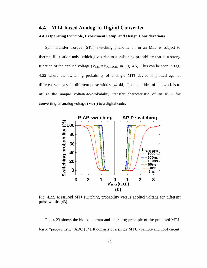
81
4.4 MTJ-based Analog-to-Digital Converter
4.4.1 Operating Principle, Experiment Setup, and Design Considerations
Spin Transfer Torque (STT) switching phenomenon in an MTJ is subject to
thermal fluctuation noise which gives rise to a switching probability that is a strong
function of the applied voltage (VMTJ =VPERTURB in Fig. 4.5). This can be seen in Fig.
4.22 where the switching probability of a single MTJ device is plotted against
different voltages for different pulse widths [42-44]. The main idea of this work is to
utilize the unique voltage-to-probability transfer characteristic of an MTJ for
converting an analog voltage (VMTJ) to a digital code.
VMTJ (a.u.)
(b)
-3 -2 -1 0 1 2 3
Sw
itc
hin
g p
rob
ab
ilit
y (
%)
100
80
60
40
20
0
1000ns500ns100ns50ns10ns5ns
P-AP switching AP-P switching
tPERTURB
Fig. 4.22. Measured MTJ switching probability versus applied voltage for different
pulse widths [43].
Fig. 4.23 shows the block diagram and operating principle of the proposed MTJ-
based “probabilistic” ADC [54]. It consists of a single MTJ, a sample and hold circuit,

82
a bidirectional pulse generator to perturb the MTJ in either anti-parallel or parallel
direction, a sense amplifier to determine the MTJ state (0 or 1), and a counter to
calculate the number of times the MTJ has resolved to a ‘1’ state. The operation
example in Fig. 4.23 (bottom) illustrates the conversion from an analog input voltage,
to a random bit stream, and finally to a digital code. The number of ‘1’s in the bit
stream is tallied for a fixed sampling window to generate the digital output count. A
longer sampling window will produce a smoother and accurate probability curve at the
expense of a longer sampling time.
VREF
Sense
Amp.
Bit stream of 0's and 1's
Counter
Bidirectional
pulse generator
CountRegister
DOUT
VIN
MTJ
Sample / hold
circuit
0001000011000100: P(1) = 25%VIN = 0.4V DOUT = 4
1011010110010010: P(1) = 50%VIN = 0.5V DOUT = 8
1111011111011010: P(1) = 75%VIN = 0.6V DOUT = 12
Note: VIN = VMTJ in Fig. 4.22
Fig. 4.23. Block diagram and operating principle of the proposed MTJ-based ADC
[54].
The experiment setup to verify the basic ADC operation is shown in Fig. 4.24.
Details of the MTJ device fabricated for this experiment is given in Fig. 4.25. Output
signals from two high speed signal generators are combined and provided to the MTJ.
A data acquisition board is used for reading out the MTJ state. To precisely control the

83
temperature of the MTJ, a film resistance heater attached to the back side of the MTJ
is driven by a software-controlled power supply. A thermocouple is used to monitor
the MTJ temperature, enabling a feedback loop with an accuracy less than 1°C. All
equipment are connected to the main computer using GPIB cables for automated
testing.
Pu
lse
Ge
ne
rato
r 1
(Ag
ile
nt
81
16
0A
TM)
Pu
lse
Ge
ne
rato
r 2
(HP
81
10
AT
M)
Power Combiner
(Picosecond
5331-104TM
)
Bias-Tee(Picosecond
5542-229TM
)
MTJ
DAQ Board
(NI USB-6343TM
)
LabViewTM
Interface
ADC
Resistance
DOUT
ResetPerturb
Read10kOhm
Power Supply
(Kepco BOP20-20TM
)
Kapton Heater
K-type
Thermocouple
Cable
Current
Control
VIN
Fig. 4.24. MTJ-based ADC experiment setup with 1mV voltage resolution and <1°C
temperature accuracy.
MgO 0.85nm
Top electrode
Co20Fe60B20 1.9nm
Co40Fe40B20 2.4nm
Ru 0.85nm
Co70Fe30 2.3nm
PtMn 15nm
Bottom electrode
(a)
(b)
150nm
60nm
0.4
0.5
0.6
0.7
0.8
0.9
1
1.1
1.2
1.3
-0.4 -0.2 0 0.2 0.4
0.40.50.60.70.80.9
11.11.21.3
-400 -200 0 200 400H (Oe)(d)
RAP
RP
TMR: 88%
RA: 5.31 Ω∙μm2
IMTJ (mA)
RAP
RP
(c)
RM
TJ (
kΩ
)R
MT
J (
kΩ
)
Thermal stability: 64
Fig. 4.25. CoFeB/MgO MTJ used in our experiments. (a) Vertical structure, (b) SEM
image, (c) R-I, and (d) R-H hysteresis curves.
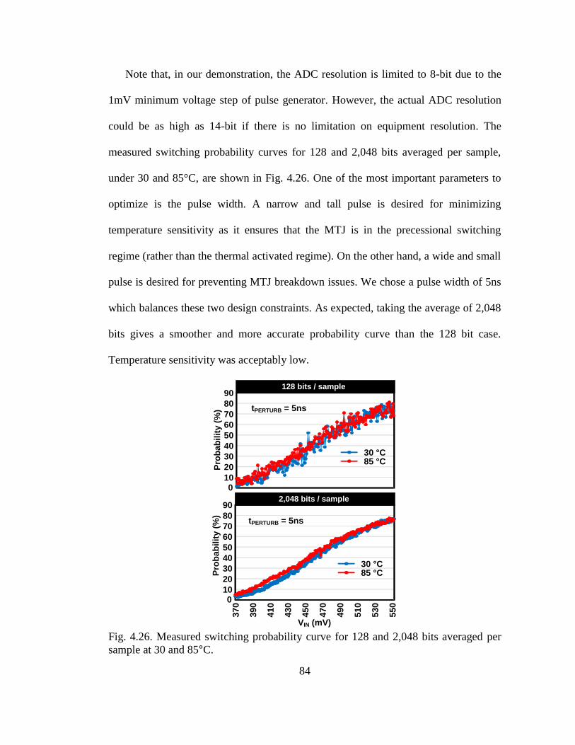
84
Note that, in our demonstration, the ADC resolution is limited to 8-bit due to the
1mV minimum voltage step of pulse generator. However, the actual ADC resolution
could be as high as 14-bit if there is no limitation on equipment resolution. The
measured switching probability curves for 128 and 2,048 bits averaged per sample,
under 30 and 85°C, are shown in Fig. 4.26. One of the most important parameters to
optimize is the pulse width. A narrow and tall pulse is desired for minimizing
temperature sensitivity as it ensures that the MTJ is in the precessional switching
regime (rather than the thermal activated regime). On the other hand, a wide and small
pulse is desired for preventing MTJ breakdown issues. We chose a pulse width of 5ns
which balances these two design constraints. As expected, taking the average of 2,048
bits gives a smoother and more accurate probability curve than the 128 bit case.
Temperature sensitivity was acceptably low.
010
20
30
40
50
60
70
80
90
Pro
ba
bilit
y (
%)
30 °C85 °C
010
20
30
40
50
60
70
80
90
37
0
39
0
41
0
43
0
45
0
47
0
49
0
51
0
53
0
55
0
VIN (mV)
Pro
ba
bilit
y (
%)
128 bits / sample
2,048 bits / sample
30 °C85 °C
tPERTURB = 5ns
tPERTURB = 5ns
Fig. 4.26. Measured switching probability curve for 128 and 2,048 bits averaged per
sample at 30 and 85°C.

85
Linearity is an important figure-of-merit for ADCs. The worst case Differential
Non-Linearity (DNL) and Integral Non-Linearity (INL) versus the number of bits
averaged per sample are shown in Fig. 4.27. Here, we assumed a 5-bit resolution. A
target DNL of 1 LSB can be met by averaging 2,048 or more random bits. However,
the INL cannot be improved just by increasing the number of bits averaged. This is
due to the inherent non-linearity of the MTJ stemming from the S-shape switching
probability curve.
0
0.5
1
1.5
2
2.5
64 512 4096# of bits / sample
30 °C85 °C
0
0.5
1
1.5
2
2.5
64 512 4096# of bits / sample
Wo
rst
ca
se
IN
L (
LS
B)
30 °C85 °C
tPERTURB = 5ns
1LSB = 4mV
tPERTURB = 5ns
1LSB = 4mV
Wo
rst
ca
se
DN
L (
LS
B)
Our target
Fig. 4.27. Worst case DNL and INL for a 5-bit ADC resolution (i.e., 1LSB=4mV)
measured under two different temperatures (30, 85°C).
4.4.2 Circuit Techniques for Improving Linearity and Input Voltage Range
To improve the linearity of the ADC further, we adopted the digital calibration
technique widely used in CMOS ADCs [48, 49]. The technique can calibrate out any
systematic non-linearity in the sensing element (e.g. amplifier, VCO, or MTJ). Fig.
4.28 shows the implementation and basic operation. During calibration mode, the
MTJ’s non-linearity is characterized by applying a slow ramp voltage generated by a

86
digital-to-analog converter to the MTJ. The quantization noise in the sampled data is
then filtered out using a moving average filter, and the results are stored in a Look-Up
Table (LUT). During normal ADC operation, the raw output of the MTJ is corrected
using the LUT mapping table. Fig. 4.29 confirms that the worst case INL at 85°C
conditions is improved from -1.5 / +1.53 LSB ( to -0.71 / +0.72 LSB while the worst
case DNL stays within -1 / +1 LSB spec. Similar improvement in INL is shown for
temperature of 30°C in Fig. 4.30.
VIN
MTJ-based
ADC1bit Accumul-
ator + DAC
Moving
Average Filter
Look Up Table
DOUT
DOUT_CAL
VIN
Pro
ba
bilit
y (
%)
MTJ
Counter
+ Register
DO
UT Linearizer
DOUT_CAL
Fig. 4.28. Compensating for MTJ non-linearity using digital calibration [48, 49].
-2
-1
0
1
2
DN
L (
LS
B)
2,048 bits / sample @ 85ºC
Before digital calibration
DNLMAX = -0.75 / +0.73
-2
-1
0
1
2
INL
(L
SB
)
Digital Out
INLMAX = -1.50 / +1.53
After digital calibration
DNLMAX = -1.00 / +0.82
Digital Out
INLMAX = -0.71 / +0.72
tPERTURB = 5ns tPERTURB = 5ns
2,048 bits / sample @ 85ºC
3 7 11 15 19 23 27 31 35 393 7 11 15 19 23 27 31 35 39
0.81 LSB
Fig. 4.29. Measured DNL (top) and INL (bottom) before and after digital calibration
@ 85°C.

87
-2
-1
0
1
2
DN
L (
LS
B)
2,048 bits / sample @ 30ºC
Before digital calibration
DNLMAX = -0.74 / +0.54
-2
-1
0
1
2
INL
(L
SB
)
Digital Out
INLMAX = -1.31 / +1.32
After digital calibration
DNLMAX = -1.00 / +0.78
Digital Out
INLMAX = -0.75 / +0.76
tPERTURB = 5ns tPERTURB = 5ns
2,048 bits / sample @ 30ºC
3 7 11 15 19 23 27 31 35 393 7 11 15 19 23 27 31 35 39
0.56 LSB
Fig. 4.30. Measured DNL (top) and INL (bottom) before and after digital calibration
@ 30°C.
VIN
Pro
ba
bilit
y (
%)
2X Input range (2∙VIN,DYN)
Proposed
scheme
VIN
Pro
ba
bilit
y (
%)
1X Input range (VIN,DYN)
VMTJ
MTJ
0V
VMTJ
MTJ
VOFFSET
Original
scheme
VOFFSET = 0V
VOFFSET = VIN,DYN
Fig. 4.31. Illustration of proposed input range enhancement technique.
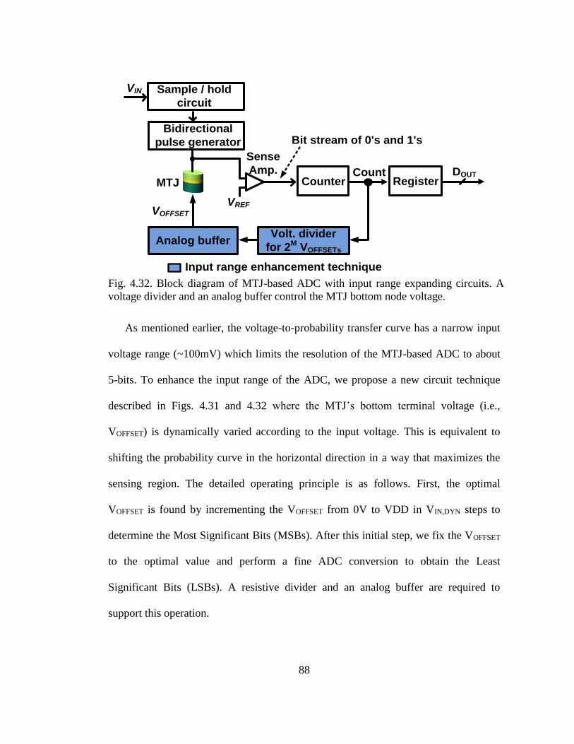
88
Volt. divider
for 2M VOFFSETs
VOFFSET
VREF
Sense
Amp.
Bit stream of 0's and 1's
Counter
Bidirectional
pulse generator
CountRegister
DOUT
VIN
MTJ
Sample / hold
circuit
Analog buffer
Input range enhancement technique
Fig. 4.32. Block diagram of MTJ-based ADC with input range expanding circuits. A
voltage divider and an analog buffer control the MTJ bottom node voltage.
As mentioned earlier, the voltage-to-probability transfer curve has a narrow input
voltage range (~100mV) which limits the resolution of the MTJ-based ADC to about
5-bits. To enhance the input range of the ADC, we propose a new circuit technique
described in Figs. 4.31 and 4.32 where the MTJ’s bottom terminal voltage (i.e.,
VOFFSET) is dynamically varied according to the input voltage. This is equivalent to
shifting the probability curve in the horizontal direction in a way that maximizes the
sensing region. The detailed operating principle is as follows. First, the optimal
VOFFSET is found by incrementing the VOFFSET from 0V to VDD in VIN,DYN steps to
determine the Most Significant Bits (MSBs). After this initial step, we fix the VOFFSET
to the optimal value and perform a fine ADC conversion to obtain the Least
Significant Bits (LSBs). A resistive divider and an analog buffer are required to
support this operation.

89
2,048 bits / sample @ 85ºC
0
10
20
30
40
50
60
70
80
90
-100 0 100 200 300 400 500 600 700 800 900 1000 1100
Pro
ba
bilit
y (
%)
VIN (mV)
0
50
100
150
200
250
300
Dig
ita
l O
utp
ut 000 001 010 011 100 101MSB: 110 111
tPERTURB
= 5ns
Voffset = -384mV -256mV -128mV 0V 128mV 256mV 384mV 512mV
Fig. 4.33. Measured probability and corresponding digital output achieving an 8x wider
input voltage range.
Fig. 4.33 shows that the input range is increased by 8 times, from 128mV (5-bit
resolution) to 1024mV (8-bit resolution). However, as mentioned earlier, actual ADC
resolution could be as high as 14-bit. By combining the digital calibration and the
input range enhancement techniques, the proposed MTJ-based ADC achieves a DNL
within -1 / +1 LSB and an INL within -0.88 / +0.87 LSB as shown in Fig. 4.34.
Similar trends are shown for temperature of 30°C in Fig. 4.35. The ADC performance
before and after applying each technique, is summarized in Fig. 4.36.

90
2,048 bits / sample @ 85ºC
Before digital calibration
INLMAX = -1.52 / +1.55
After digital calibration
-2
-1
0
1
2
DN
L (
LS
B)
DNLMAX = -1.00 / +1.00
tPERTURB = 5ns
Digital Out
-2
-1
0
1
2
INL
(L
SB
)
DNLMAX = -1.00 / +1.00
tPERTURB = 5ns
INLMAX = -0.88 / +0.87
Digital Out
2,048 bits / sample @ 85ºC
0 28 56 84 112 140 168 196 224 252 0 28 56 84 112 140 168 196 224 252
0.68 LSB
Fig. 4.34. Measured DNL (top) and INL (bottom) before and after digital calibration
using the proposed input range enhancement technique @ 85°C.
2,048 bits / sample @ 30ºC
Before digital calibration
INLMAX = -1.47 / +1.47
After digital calibration
-2
-1
0
1
2
DN
L (
LS
B)
DNLMAX = -1.00 / +1.00
tPERTURB = 5ns
Digital Out
-2
-1
0
1
2
INL
(L
SB
)
DNLMAX = -1.00 / +1.00
tPERTURB = 5ns
INLMAX = -0.83 / +0.84
Digital Out
2,048 bits / sample @ 30ºC
0 28 56 84 112 140 168 196 224 252 0 28 56 84 112 140 168 196 224 252
0.63 LSB
Fig. 4.35. Measured DNL (top) and INL (bottom) before and after digital calibration
using the proposed input range enhancement technique @ 30°C.
Original MTJ-based ADC
+ Digital calibration
+ Digital calibration
+ Input range enhancement
DNLMAX
(LSB)
0.74 1.32
1.00 0.76
1.00 0.84
Bits
5
5
8
0.75 1.53
1.00 0.72
1.00 0.88
Bits
5
5
8
30 ºC 85 ºC
2,048 bits / sample
Input
range
128mV
(X1)
128mV
(X1)
1024mV
(X8)
DNLMAX
(LSB)INLMAX
(LSB)
INLMAX
(LSB)
Fig. 4.36. ADC performance summary table.

91
4.5 MTJ-based Temperature Sensor
4.5.1 Operating Principle and Design Considerations
As the multi-core era arrives, on-chip temperature sensors are widely used in VLSI
thermal monitoring and power management circuits to optimize the system
performance. Multi-location hot-spots temperature monitoring in modern multi-core
processors makes it possible to limit leakage and improve computational capabilities
through load balancing [55]. In the meantime, the continuous scale-down of process
technologies and the demand for battery-operation require analog function blocks such
as temperature sensors to operate with low supply voltages. The main idea of this
work is to utilize the unique temperature-to-probability transfer characteristic in the
thermal activated switching regime of an MTJ for converting a temperature to a
probability.
Fig. 4.37. Measured switching (perturb) pulse width versus pulse amplitude at 50%
switching probability from 0.5 ns to 0.1 s for AP to P switching [42].

92
In MTJ switching, two distinct temperature dependence of the switching current
density are apparent due to the two switching modes [42, 57]: a switching current
density decrease with increasing temperature in the wide (>100 ns) and small pulse
regime, a result of thermally activated switching, but no decrease in the narrow (<10
ns) and tall pulse regime, as a result of precessional switching. Fig. 4.37 shows the
measured critical switching pulse amplitude as a function of the pulse width. Each
data point corresponds to the pulse amplitude and pulse width at 50% switching
probability. For short pulses (red points in the figure), the STT induced switching
process is in the precessional switching mode. It is a dynamic reversal process driven
by the spin momentum transfer, almost independent of the thermal agitation. The
switching probability distribution is mainly caused by the initial position dispersion
from thermal fluctuation. While for the long pulse (blue points in the figure), the STT
induced switching is in the thermal activation mode, mainly driven by thermal
agitation. The initial position distribution from thermal fluctuation does not make
much difference on the final switching probability. Dynamic reversal mode is an
intermediate regime between the precessional mode and the thermal activation mode.
The magnetization reversal is contributed by a combination of spin momentum
transfer and thermal agitation and the exact boundaries of the three STT induced
switching modes are difficult to determine.
For the temperature sensor demonstration, a wide and small pulse is desired for
maximizing temperature sensitivity as it ensures that the MTJ is in the thermal
activated switching regime (rather than the precessional regime). Measured data in Fig.
4.38 confirm that the temperature dependence increases as perturb pulse width

93
increases over 100ns. In our demonstration, we chose a pulse width of 500ns to
enhance the temperature sensing resolution. VPERTURB of 300mV was chosen for the
following temperature sensing experiments as shown in Fig. 4.39. To verify the basic
temperature sensor operation, the experiment setup shown in Fig. 4.24 was used.
0
10
20
30
40
50
60
70
80
90
100
240 280 320 360 400 440 480 520 560 600 640 680
Pro
ba
bilit
y (
%)
Perturb amplitude (mV)
10,000 bits / sample
tPERTURB = 500ns @ 30ºC
tPERTURB = 500ns @ 85ºC
tPERTURB = 100ns @ 30ºC
tPERTURB = 100ns @ 85ºC
tPERTURB = 5ns @ 30ºC
tPERTURB = 5ns @ 85ºC
tPERTURB ↑
temperature
dependence ↑
Fig. 4.38. Measured switching probability with different perturb pulse widths
(tPERTURB = 5ns, 100ns, and 500ns) @ 30, 85°C.
260 280 300 320 340 360
Perturb amplitude (mV)
0
10
20
30
40
50
60
70
80
90
100
Pro
ba
bilit
y (
%)
tPERTURB = 500ns @ 30ºC
tPERTURB = 500ns @ 85ºC
10,000 bits / sample
@ VPERTURB = 300mV
Temperature
sensing range
Fig. 4.39. Measured switching probability with different temperatures (30 and 85°C)
@ tPERTURB = 500ns. VPERTURB of 300mV was chosen for the following temperature
sensing experiments.

94
4.5.2 Temperature Sensing Experiment Results
Fig 4.40(a) shows the measured switching probability as a function of temperature.
Our experiment data show that the switching probability with a pulse width of 500ns
exhibits good linearity in temperature range between 30 and 90°C with a slope (i.e.,
temperature coefficient) of 0.51 [%/°C]. Measured data in Fig. 4.40(b) confirm that
the worst-case temperature error with 2-temperature point calibration is less than
+0.60 / -0.91°C.
30
35
40
45
50
55
60
65
70
75
80
20 30 40 50 60 70 80 90 100
Pro
ba
bilit
y (
%)
Temperature (ºC)
(a)
-3
-2
-1
0
1
2
3
20 30 40 50 60 70 80 90 100
Te
mp
era
ture
err
or
(ºC
)
@ tPERTURB = 500ns,
VPERTURB = 300mV
20,000 bits / sample
Temp. sensing range: 30 ~ 90 ºC
Temp. coefficient: 0.51 (%/ºC)
Temperature (ºC)
(b)
2-temperature point
caribration
Worst-case temp. error: +0.60 / -0.91 ºC
20,000 bits / sample
@ tPERTURB = 500ns,
VPERTURB = 300mV
Fig. 4.40. (a) Measured switching probability as a function of temperature @ tPERTURB
= 500ns, VPERTURB = 300mV. (b) Measured temperature error with 2-temperature point
calibration.

95
4.6 Conclusion
Spin Transfer Torque (STT) switching phenomenon in a Magnetic Tunnel
Junction (MTJ) is subject to random thermal fluctuation noise which gives rise to a
switching probability that is a strong function of the applied “perturb” voltage and
pulse width. In this work, we have experimentally demonstrated for the first time, new
classes of TRNG, ADC, and temperature sensor based on the random switching
behavior of an MTJ.
For the TRNG demonstration, we propose a conditional perturb and real-time
output probability tracking scheme to achieve a 100% bit efficiency (or 100% useable
bits) while improving the reliability, speed, and power consumption. For the ADC
demonstration, two circuit techniques were implemented to improve the ADC linearity
and increase the input voltage range. The proposed ADC achieves an 8-bit resolution
with excellent linearity at 30 and 85°C. For showing the feasibility of temperature
sensor, an MTJ in the thermal activated switching regime was used to show the
temperature dependence of the switching probability. Our experiment data show that
the switching probability with a pulse width of 500ns exhibits good linearity in
temperature range between 30 and 90°C with a slope (i.e., temperature coefficient) of
0.51 [%/°C]. The worst-case temperature error with 2-temperature point calibration is
less than +0.60 / -0.91°C.
Our demonstrations with the promising experiment data show the feasibility of
MTJ technology for non-memory mixed-signal applications.
96
Chapter 5. A Comprehensive Study on Interface
Perpendicular MTJ (I-PMTJ) Variability
This chapter introduces a comprehensive study on Interface Perpendicular MTJ (I-
PMTJ) variability [68]. In this work, we quantify the impact of the free layer thickness
(tF) variation on thermal stability factor (Δ) and switching current (IC) variability in I-
PMTJ. The Δ variability shows considerably more tF variation dependency compared
to IC variability counterpart, offering smaller increase of ∆ and IC as tF variation is
improved to make all random MTJ samples meet a retention time specification.
5.1 Introduction
Spin transfer torque MRAM (STT-MRAM) is one of the promising candidates as a
scalable nonvolatile memory with high density, and CMOS compatibility [58, 59]. I-
PMTJ has been demonstrated with the goal of reducing the switching current while
maintaining sufficient nonvolatility [60]. However, previous studies report that I-
PMTJ suffers from process-dependent dimensional variations, thus it remains one of
the major constrains in achieving high performance STT-MRAM [61, 62]. This paper
presents a comprehensive study on process-dependent dimensional variability of I-
PMTJ, especially focusing on estimating the impact of tF variation on Δ and IC
variability. For a practical analysis, our physics-based macrospin SPICE model [63]
captures the key physics of STT switching in PMTJ by incorporating all of the above
mentioned PMTJ dimension-dependent parameters into the Landau-Lifshitz-Gilbert
(LLG) equation.

97
5.2 Interface Perpendicular Magnetic Tunnel Junction (I-
PMTJ)
One of the key challenges on the MTJ technology development is to reduce the
switching current without compromising nonvolatility. As explained in Chapter 4.2,
magnetic anisotropy decides the energetic preference of the magnetization direction
often referred to as the easy axis. Depending on the source of the anisotropy, the MTJs
can be classified into the following three categories: shape anisotropy-based in-plane
MTJ (IMTJ), crystal anisotropy-based perpendicular MTJ (C-PMTJ), and interface
anisotropy-based perpendicular MTJ (I-PMTJ).
For IMTJ, thermal stability is primarily determined by the shape anisotropy. The
physical origin of shape anisotropy is the demagnetizing field (Hd) which is strongest
in the direction of the magnet with the shortest dimension (e.g., z-direction). The Hd
basically acts against the magnetization thereby reducing the total magnetic moment.
The free layer of the IMTJ is in the shape of an elongated thin film, thus, the
magnetization tries to stay in the x-y plane resulting in in-plane magnetization. The in-
plane magnetization has to overcome a large out-of-plane demagnetizing field (Hdz),
which attempts to keep the magnetization within the plane, giving rise to a large
switching current. However, anisotropy behavior of a CoFeB based free layer shifts
from in-plane to perpendicular as its tF becomes thinner than a critical thickness (tc) of
~1.5nm [60]. This so-called interface anisotropy in a CoFeB/MgO based MTJ stack
can be utilized for the free layer. Perpendicular magnetization can provide a lower
switching current since the Hdz assists the STT switching by partially canceling out the

98
perpendicular anisotropy field (HK) as shown in Fig. 5.1(a). Since the CoFeB/MgO
structure is widely used as a standard material system for IMTJ’s, the I-PMTJ
provides high TMR as well as low switching current while taking advantage of the
mature fabrication process of IMTJ.
Free layer
Tunnel barrier
Pinned layer
1.00.5
My-
1.01.0
0.0-
0.5
-
1.0-
0.5 0.00.5
0.0
0.5
1.0
-0.5
-1.0
Mx
Mz
(a)
(b)
Fig. 5.1. (a) Stack and magnetization configuration and (b) Dynamic spin motion of I-
PMTJ and [63].
To achieve the fast STT switching and long retention time in CoFeB/MgO based I-
PMTJ, the junction diameter should be reduced. However, to further reduce the device
diameter, enhancement of Δ is required. In order to increase Δ of CoFeB/MgO based
I-PMTJ, an increase of tF is required. However, the tF should be thinner than tc to

99
maintain the perpendicular magnetic easy axis. To overcome this, a double
CoFeB/MgO interface structure [66] was introduced as shown in Fig 5.2. the
measured data confirms that the double-interface structure achieve a higher Δ than
single-interface structure with the same free layer diameter (D in the figure). In our
case study, the double CoFeB/MgO based I-PMTJ was considered.
Fig. 5.2. (a) Stack structure of magnetic tunnel junction with double-interface structure
and (b) single-interface structure. (c) Switching probability as a function of pulse
magnetic field amplitude for MTJs with double-interface structure and (d) single-
interface structure [66].
Previous studies report that PMTJ suffers from process-dependent dimensional
variations, thus it remains one of the major constrains in achieving high performance
STT-MRAM [61, 62]. As shown in the equations of Fig. 5.3, the anisotropy field (Hk)
and free layer volume (V) are functions of I-PMTJ dimensions, hence their variations
result in variation of STT switching characteristics such as thermal stability factor (Δ)

100
and switching current (IC). The Hk of PMTJ has a strong dependency on relative ratio
between the free layer thickness (tF) and the critical thickness (tc) [60]. The equations
of Fig. 5.3 suggest that the tF variation differently affects the PMTJ dimension-
dependent parameters (gray circles in the figure), resulting in either increasing or
decreasing Δ and/or IC. This paper presents a comprehensive study on process-
dependent dimensional variability of I-PMTJ, especially focusing on estimating the
impact of tF variation on Δ and IC variability. For a practical analysis, our physics-
based macrospin SPICE model [63, 67] captures the key physics of STT switching in
PMTJ by incorporating all of the above mentioned PMTJ dimension-dependent
parameters into the Landau-Lifshitz-Gilbert (LLG) equation.
Fig. 5.3. The anisotropy field (Hk), thermal stability factor (∆), and switching current
(IC) in interface perpendicular magnetic tunnel junction (I-PMTJ) show a strong
dependency of process-dependent dimensional variations.

101
5.3 Methodology for I-PMTJ Variability Analysis
Our variability analysis is based on determining the degree of Δ for a target chip
failure rate as shown in Fig. 5.4. Here, we assume a STT-MRAM L3 cache with
64MB density for server processor as a target memory system. The 7.95x10⁻⁷ chip
failure rate is set by the repair capability and corresponding Δ of 70 for 10 years of
retention is estimated [64].
Magnet dimensions to meet ?
Ic (tsw=5ns)
Quadratic mean initial angle:
Macrospin simulationDimension dependent HKeff
Free layer magnetization:
Fixed layer magnetization:
Spin torque amplitude:
LLG solving:
Δ
STT components (Precessional switching)
,)/(2 2
Tk
VMNtt
B
sdzFc
F
cs
t
tMK
22
sF
sst
Met
JA
2
)](),(),([4
)]()/2(,0,0[)(
tMNtMNtMNM
tMMKtH
zdzydyxdxs
zSeffK
)()(1 2
istKeffKeff MMMAHMMHMdt
Md
],,[ iziyixi MMMM
)](),(),([)( tMtMtMtM zyx
)2/1(sin 1
W, L, tF Ndx, Ndy, Ndz
W L tF
Monte Carlo simulation Random variables extraction with 3σ
Variability analysisEvaluation of IC, Δ, tretention variability
Magnet material
specification
Ms, a, P, tc
System specificationFchip: Chip failure rate, m: Memory size, tretension: Retention time
)exp(exp10
retentionchip
tmF
W L tF 3σ 3σ 3σ
Fig. 5.4. Variability analysis using a physics-based macrospin SPICE model.

102
The variation factors and realistic I-PMTJ material parameters [51], [60], [62] used
in this work are shown in Fig. 5.5. A double MgO interface [62] is considered to scale
the IC down and increase the Δ for meeting the system specification. The tF-dependent
damping factor (α) in CoFeB is also considered for realistic analysis. To estimate the
impact of process-dependent dimensional variations on PMTJ variability, appropriate
values of the variation (3σ/μ) in the free layer width and length are set to 12%
according to the ITRS roadmap. Moreover, the variation (3σ/μ) of tF is varied from 4%
to 9% with 1% step to evaluate its dependency on Δ and IC variability. Each variation
parameter is assumed to have a normal distribution with ±3 standard deviation (σ).
The Monte Carlo simulator extracts the 1000 random variables with ±3σ for all the
above mentioned dimension-dependent parameters, then, our physics-based macrospin
SPICE model [63, 67] estimates each IC, Δ, and tretention variability for a given
switching time (tsw).
64MB L3 cache memory, Δ = 70 for 10yrs retention
Sat. Magnetization, MS (103A/m)
Interface
1077
Polarization factor, P 0.6
Length, width of free layer,
L, W (nm)
µ=22, µ=22
(3σ/µ=12%***)
Gilbert Damping, a tF dependent**
Thickness of free layer, tF (nm)µ=2.78
(3σ/µ=4***~9%)
Effective critical thickness, tC (nm) 3 (1.5 x 2, double MgO interface*)
Quantity PMTJ [51], [60], [62]
* To increase the Δ for 10yrs retention, double MgO interface is used [62]
** tF dependent a is used [60], *** ITRS roadmap
Anisotropy source
Fig. 5.5. Variation factors and realistic PMTJ material parameters used in the
variability analysis.

103
5.4 Variability Analysis on I-PMTJ
Fig. 5.6(a) shows the simulated IC as a function of tsw at 50% switching probability.
Note that our model demonstrates realistic dynamic spin motions based on measured
data [42]. A constant tsw of 5ns was chosen for following variability simulations.
I C (μ
A)
Oc
cu
rren
ce
0
50
100
150
200
250
300
350
400
450
500
0 2 4 6 8 10
0
50
100
150
200
250
300
350
400
450
500
20 40 60 80 100
358K, Δ = 70 for 10yrs retention
358K, Δ = 70 for 10yrs retention
μ=61.22, σ/μ=5.6%
@ tSW =5ns
tSW (ns)
(a)
IC (μA)
(b)
3σ/µ of W, L = 12%, 3σ/µ of tF = 4%
tSW =5ns
Fig. 5.6. (a) IC as a function of tsw and (b) IC variation under free layer W, L variation
of 12% and tF variation of 4% (tsw=5ns). IC roughly follows a Gaussian distribution.

104
Occ
urr
en
ce
? (Thermal Stability Factor)
(a)
Occu
rren
ce
t retention (s)
10yrs
0
50
100
150
200
250
300
350
400
450
500
50 60 70 80 90 100
μ = 70.17, σ/μ = 5.2%
0
50
100
150
200
250
300
101
105
109 10
1310
17
358K, Δ = 70 for 10yrs retention
σ = 2.2e+12
@ tSW =5ns
@ tSW =5ns
3σ/µ of W, L = 12%, 3σ/µ of tF = 4%
358K, Δ = 70 for 10yrs retention3σ/µ of W, L = 12%, 3σ/µ of tF = 4%
(b) Fig. 5.7. Variation of (a) ∆ and (b) tretention under free layer W, L variation of 12% and
tF variation of 4%. ∆ and log(tretention) roughly follow Gaussian distributions. Over 40%
of the MTJs fail to meet the 10 year retention time target.
As shown in Figs. 5.6(b) and 5.7, each IC, Δ, and log(tretention) variability roughly
follow Gaussian distributions under free layer W, L variation of 12% and tF variation
of 4%. 5.7(b). Fig. 5.8 shows the tF variation dependency on ∆ variability. Simulation
result indicates that the ∆ variability has a strong linear dependency on tF variation.
Variability trend of tretention is projected directly from the variability trend of ∆ [62].
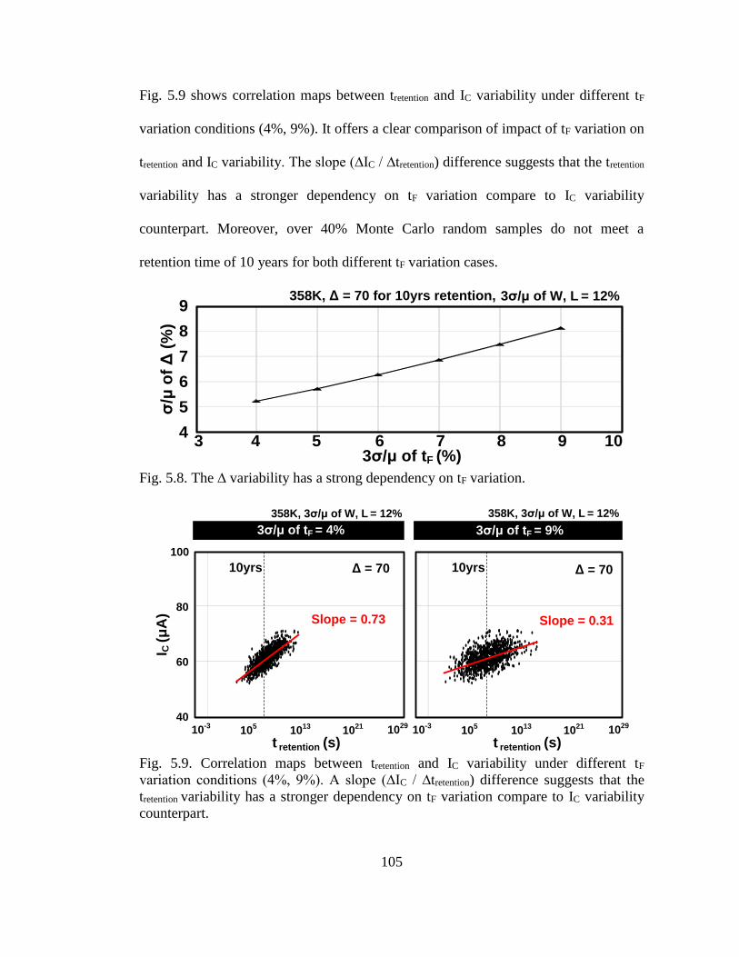
105
Fig. 5.9 shows correlation maps between tretention and IC variability under different tF
variation conditions (4%, 9%). It offers a clear comparison of impact of tF variation on
tretention and IC variability. The slope (∆IC / ∆tretention) difference suggests that the tretention
variability has a stronger dependency on tF variation compare to IC variability
counterpart. Moreover, over 40% Monte Carlo random samples do not meet a
retention time of 10 years for both different tF variation cases.
4
5
6
7
8
9
3 4 5 6 7 8 9 103σ/μ of tF (%)
σ/μ
of Δ
(%
)
358K, Δ = 70 for 10yrs retention, 3σ/μ of W, L = 12%
Fig. 5.8. The ∆ variability has a strong dependency on tF variation.
3σ/μ of tF = 4%
40
60
80
100
10-3
105
1013
1021 10
29
t retention (s)10
-310
510
1310
21 1029
t retention (s)
10yrs 10yrs
3σ/μ of tF = 9%
358K, 3σ/μ of W, L = 12%
I C (µ
A) Slope = 0.73
Δ = 70
358K, 3σ/μ of W, L = 12%
Δ = 70
Slope = 0.31
Fig. 5.9. Correlation maps between tretention and IC variability under different tF
variation conditions (4%, 9%). A slope (∆IC / ∆tretention) difference suggests that the
tretention variability has a stronger dependency on tF variation compare to IC variability
counterpart.

106
Fig. 5.10 Increasing ∆ would be considered to make all of random samples meet a
target of 10 years retention [65].
3σ/μ of tF = 4% 3σ/μ of tF = 9%
358K, 3σ/μ of W, L = 12% 358K, 3σ/μ of W, L = 12%
10-3
105
1013
1021 10
29
t retention (s)
I C (µ
A)
10yrs
10-3
105
1013
1021 10
29
t retention (s)
10yrs
40
60
80
100
∆ = 82
∆ = 70
∆ = 87
∆ = 70
Fig. 5.11. Re-plotted correlation maps after increasing ∆.
Increasing ∆ shown in Fig. 5.10 would be considered to make all of random
samples meet a target of 10 years retention [65]. However, increase of IC is
unavoidable for increasing ∆. After increasing ∆, the correlation maps are re-plotted in
Fig. 5.11 compared to Fig. 5.9 (gray dots). Results shown in Fig. 5.12 indicate that the

107
2.3x steeper slope (∆IC / ∆tretention) under 4% tF variation compare to 9% counterpart
offers smaller ∆ increase (82 rather than 87), requiring a 0.6x smaller IC increase to
make all random MTJ samples have a longer retention time than 10 years.
∆ for 10yrs tretention
IC (μA)
70
∆
Quantity
∆ for tretention,Min> 10yrs
IC (μA)
82
Remark (required IC for increasing ∆)
Typical
∆ design
When ∆ is
increased
3σ/μ of tF = 4% 3σ/μ of tF = 9%
Avg.
61.22
70.17
Avg.
68.11
σ/μ
5.6%
5.2%
σ/μ
5.7%
6.89μA (0.6x)
70
87
Avg.
61.31
70.27
Avg.
72.03
σ/μ
5.7%
8.1%
σ/μ
5.7%
10.72μA (1x)
358K, 3σ/μ of W, L = 12%
∆IC / ∆tretention (μA/s) 0.73 (2.3x) 0.31 (1x)
Fig. 5.12. The 2.3x steeper slope (∆IC / ∆tretention) under 4% tF variation compare to 9%
counterpart offers smaller increase in ∆ (82 rather than 87), requiring a 0.6x smaller
increase in IC to make all of random samples have a longer retention time than 10
years.

108
5.5 Conclusion
A comprehensive study on I-PMTJ variability was performed with realistic
parameters using a physics-based macrospin SPICE model. Our MTJ model
incorporates dimension-dependent effective anisotropy field into LLG equation.
Simulation data show that the IC, ∆ and log(tretention) roughly follow Gaussian
distributions. Variability of ∆ and tretention is more sensitive to tF variation compared to
IC variability. Tighter tF control allows a smaller increase in ∆ and IC to ensure all
MTJ’s meet a 10 year retention time.

109
Chapter 6 Summary
In this thesis, firstly, on-chip circuit design techniques for characterizing latent
Plasma-Induced Damage (PID) and mitigating short-term Vth instability issues in
SAR ADCs were implemented in 65nm CMOS process. Secondly, spintronics-based
mixed-signal circuits (i.e., TRNG, ADC, and temperature Sensor) were experimentally
demonstrated for the first time. At last, a comprehensive study on interface
perpendicular MTJ (I-PMTJ) variability was presented.
In Chapter 2, we have developed two array-based on-chip monitoring circuits for
characterizing latent PID efficiently. First of all, an array-based PID-induced TDDB
monitoring circuit with various antenna structures is presented for efficient collection
of massive PID breakdown statistics. Measured Weibull statistics from a 12x24 array
implemented in 65nm show that DUTs with plate type antennas have a shorter lifetime
compared to their fork type counterparts suggesting greater PID effect during the
plasma ashing process. Secondly, a PID-induced BTI monitoring circuit based on a
ring oscillator array is proposed for collecting high-quality BTI statistics. Two types of
ring oscillators, PID protected and PID damaged, with built-in antenna structures were
designed to separate PID from other effects. Measured frequency statistics from a
65nm test-chip shows a 1.15% shift in the average frequency as a result of PID.
In Chapter 3, we proposed the stress equalization and stress removal techniques for
mitigating short-term Vth instability issues in SAR ADCs. The circuit techniques are
verified using an 80kS/s 10-bit differential SAR ADC fabricated in a 65nm LP CMOS
process. The proposed techniques are particularly effective in enhancing the

110
performance of high resolution and low sample rate SAR ADCs which are known to
be more susceptible to short-term Vth degradation and recovery effects induced by
Bias Temperature Instability (BTI). Experimental data shows that the proposed
techniques can reduce the worst case DNL by 0.90 LSB and 0.77 LSB, respectively,
compared to a typical SAR ADC.
In Chapter 4, we experimentally demonstrated the new classes of TRNG, ADC,
and temperature sensor based on the random switching behavior of an MTJ for the
first time. A major highlight of TRNG work is the conditional perturb and real-time
output probability tracking scheme which further enhances the throughput, power
consumption and lifetime of the MTJ based TRNG without compromising bit
efficiency. In the ADC demonstration, two circuit techniques were implemented to
improve the ADC linearity and increase the input voltage range. The proposed ADC
achieves an 8-bit resolution with excellent linearity at 30 and 85°C. For showing the
feasibility of temperature sensor, an MTJ in the thermal activated switching regime
was used to show the temperature dependence of the switching probability. Our
experiment data show that the switching probability with a pulse width of 500ns
exhibits good linearity in temperature range between 30 and 90°C with a slope (i.e.,
temperature coefficient) of 0.51 [%/°C]. The worst-case temperature error with 2-
temperature point calibration is less than +0.60 / -0.91°C.
In Chapter 5, we conducted a comprehensive study on process-dependent
dimensional variability of I-PMTJ, especially focusing on estimating the impact of the
free layer thickness (tF) variation on thermal stability factor (Δ) and switching current
(IC) variability. The Δ variability shows considerably more tF variation dependency

111
compared to IC variability counterpart, offering smaller increase of ∆ and IC as tF
variation is improved to make all random MTJ samples meet a retention time
specification.

112
References
[1] H. Shin, C. King, C. Hu, "Thin Oxide Damage by Plasma Etching and Ashing
Processes," in Proc. IEEE Int. Reliability Physics Symp., pp. 37-41, 1992.
[2] Z. Wang, J. Ackaert, A. Scarpa, C. Salm, F.G. Kuper, M. Vugts, “Strategies to
cope with plasma charging damage in design and layout phases,” in Proc.
IEEE Int. Conf. Integrated Circuit Design and Technology, pp. 91-98, 2005.
[3] P.H. Chen, "Beat the competition: a knowledge-based design process
addressing the antenna effect and cell placement," IEEE Circuits & Devices
Magazine, vol. 20, no. 3, pp. 18-27, 2004.
[4] T.B. Hook, D. Harmon and C. Lin, “Detection of thin oxide (3.5nm) dielectric
degradation due to charging damage by rapid-ramp breakdown,” in Proc. IEEE
Int. Reliability Physics Symp. (IRPS), pp. 377-388, 2000.
[5] P. Simon, J.M. Luchies, W. Maly, “Identification of plasma-induced damage
conditions in VLSI designs,” IEEE Trans. Semicond. Manuf., vol. 13, no. 2, pp.
136-144, 2000.
[6] W. Lai, D. Harmon, T. Hook, V. Ontalus, J. Gambino, “Ultra-thin Gate
Dielectric Plasma Charging Damage in SOI Technology,” in Proc. IEEE Int.
Reliability Physics Symp. (IRPS), pp. 370-373, 2006.
[7] W.T. Weng, A.S. Oates, T.-Y. Huang, “A Comprehensive Model for Plasma
Damage Enhanced Transistor Reliability Degradation,” in Proc. IEEE Int.
Reliability Physics Symp. (IRPS), pp. 364-369, 2007.
[8] X. Garros, G. Reimbold, O. Louveau, et al., “Process damages in HfO2/TiN
stacks: the key role of H0 and H2 anneals,” in Proc. IEEE Int. Electron
Devices Meeting (IEDM), pp. 191-194, 2005.

113
[9] P.J. Liao, et al., “Physical Origins of Plasma Damage and Its Process/Gate
Area Effects on High-k Metal Gate Technology,” in Proc. IEEE Int. Reliability
Physics Symp. (IRPS), pp. 4C.3.1-4C.3.5, 2013.
[10] W. Choi, P. Jain, C.H. Kim, “An array-based circuit for characterizing latent
Plasma-Induced Damage,” in Proc. IEEE Int. Reliability Physics Symp. (IRPS),
pp. 4A.3.1-4A.3.5, 2013.
[11] P. Simon, W. Maly, J.M. Luchies, R. Antheunis, “Multiplexed antenna
monitoring test structure [plasma charging damage],” in Proc. Int. Symp. on
Plasma Process-Induced Damage, pp. 205-208, 1998.
[12] A. Martin, C. Bukethal, and K.-H. Ryden, “Fast Wafer Level Reliability
Monitoring: Quantification of Plasma-Induced Damage Detected on
Productive Hardware,” IEEE Trans. Device and Materials Reliability, vol. 9,
no. 2, pp. 135-144, 2009.
[13] Robin Degraeve, Guido Groeseneken, Rudi Bellens, Jean Luc Ogier, Michel
Depas, Philippe J. Roussel, and Herman E. Maes, “New Insights in the
Relation Between Electron Trap Generation and the Statistical Properties of
Oxide Breakdown,” IEEE Trans. Electron Devices, vol. 45, no. 4, pp. 904–911,
1998.
[14] D. Ielmini, M. Manigrasso, F. Gattel, and M.G. Valentini, “A new NBTI
model based on hole trapping and structural relaxation in MOS dielectrics,”
IEEE Trans. Electron Devices, vol. 56, no. 9, pp. 1943–1952, 2009.
[15] T. Grasser and B. Kaczer, “Evidence that two tightly coupled mechanisms are
responsible for negative bias temperature instability in oxynitride MOSFETs,”
IEEE Trans. Electron Devices, vol. 56, no. 5, pp.1056–1062, 2009.
114
[16] T.H. Kim, R. Persaud, C.H. Kim, “Silicon Odometer: An On-Chip Reliability
Monitor for Measuring Frequency Degradation of Digital Circuits,” in Proc.
VLSI Circuits Symp., pp. 122-123, 2007.
[17] T.H. Kim, R. Persaud, and C.H. Kim, "Silicon Odometer: An On-Chip
Reliability Monitor for Measuring Frequency Degradation of Digital Circuits,"
IEEE J. Solid-State Circuits, vol. 43, no. 4, pp. 874-880, 2008.
[18] J. Keane, D. Persaud, and C.H. Kim, "An All-in-One Silicon Odometer for
Separately Monitoring HCI, BTI, and TDDB," in Proc. VLSI Circuits Symp.,
pp. 109-109, 2009.
[19] J. Keane, X. Wang, D. Persaud, and C.H. Kim, "An All-in-One Silicon
Odometer for Separately Monitoring HCI, BTI, and TDDB," IEEE J. Solid-
State Circuits, vol. 45, no. 4, pp. 817-829, 2010.
[20] J. Keane, W. Zhang, C.H. Kim, “An On-Chip Monitor for Statistically
Significant Circuit Aging Characterization,” in Proc. IEEE Int. Electron
Devices Meeting (IEDM), pp. 4.2.1-4.2.4, 2010.
[21] J. Keane, W. Zhang, C.H. Kim, "An Array-Based Odometer System for
Statistically Significant Circuit Aging Characterization," IEEE J. Solid-State
Circuits, vol. 46, no. 10, pp. 2374-2385, 2011.
[22] J. Keane and C.H. Kim, "An Odometer for CPUs," IEEE Spectrum, vol. 48, no.
5, pp. 28-33, 2011.
[23] W. Choi, S. Satapathy, J. Keane, and C.H. Kim, “A Test Circuit Based on a
Ring Oscillator Array for Statistical Characterization of Latent Plasma-Induced
Damage,” in Proc. IEEE Custom Integrated Circuits Conference (CICC), pp.
1-4, Sep. 2014.
115
[24] P. Jain, J. Keane, C.H. Kim, “An array-based Chip Lifetime Predictor macro
for gate dielectric failures in core and IO FETs,” in Proc. European Solid-State
Device Research Conf. (ESSDERC), pp. 262-265, 2012.
[25] S. Rangan, et al., “Universal recovery behavior of negative bias temperature
instability [PMOSFETs],” in Proc. IEEE Int. Electron Devices Meeting
(IEDM), pp. 14.3.1-14.3.4, 2003.
[26] H. Reisinger, et al., “Analysis of NBTI Degradation- and Recovery-Behavior
Based on Ultra Fast VT-Measurements,” in Proc. IEEE Int. Reliability Physics
Symp. (IRPS), pp. 448-453, 2006.
[27] S. Drapatz, et al., “Impact of fast-recovering NBTI degradation on stability of
large-scale SRAM arrays,” in Proc. IEEE European Solid-State Device
Research Conf. (ESSDERC), pp. 146-149, 2010.
[28] V. Huard, et al., “NBTI degradation: From transistor to SRAM arrays,” in Proc.
IEEE Int. Reliability Physics Symp. (IRPS), pp. 289-300, 2008.
[29] K. Rott, et al., “Impact and measurement of short term threshold instabilities in
MOSFETs of analog circuits,” in Proc. IEEE Int. Integrated Reliability
Workshop (IRW), pp. 31-34, 2012.
[30] C. Yilmaz, et al., “Modeling of NBTI-recovery effects in analog CMOS
circuits,” in Proceedings of IEEE Int. Reliability Physics Symp. (IRPS), pp.
2A.4.1-2A.4.4, 2013.
[31] W. Liu, et al., “A 12b 22.5/45MS/s 3.0mW 0.059mm2 CMOS SAR ADC
achieving over 90dB SFDR,” in Proc. IEEE Int. Solid-State Circuits Conf.
(ISSCC), pp. 380-381, 2010.
[32] X. Wang, et al., “SRAM Read Performance Degradation under Asymmetric
NBTI and PBTI Stress: Characterization Vehicle and Statistical Aging Data,”

116
in Proc. IEEE Int. Custom Integrated Circuits Conference (CICC), pp. 1-4,
2014.
[33] Anand T. Krishnan, et al., “NBTI Impact on Transistor & Circuit: Models,
Mechanisms & Scaling Effects,” in Proc. IEEE Int. Electron Devices Meeting
(IEDM), pp. 249-352, 2003.
[34] K. Mistry, et al., “A 45nm Logic Technology with High-k + Metal Gate
Transistors, Strained Silicon, 9Cu Interconnect Layers, 193nm Dry Patterning,
and 100% Pb-free Packaging,” in Proc. IEEE Int. Electron Devices Meeting
(IEDM), pp. 247-250, 2007.
[35] M. Chudzik, et al., “High-performance high-k/metal gates for 45nm CMOS
and beyond with gate-fist processing,” in Proc. VLSI Technology Symposium,
pp. 194-195, 2007.
[36] C. Zhou, X. Wang, Y. Zhu, V. Janapa Reddi, and C.H. Kim, "Estimation of
Instantaneous Frequency Fluctuation in a Fast DVFS Environment Using an
Empirical BTI Stress-Relaxation Model", in Proc. IEEE Int. Reliability
Physics Symp. (IRPS), 2D.2.1-2D.2.6, Jun. 2014
[37] W. Choi, H. Kim, and C.H. Kim, "Circuit Techniques for Mitigating Short-
Term Vth Instability Issues in Successive Approximation Register (SAR)
ADCs", in Proc. IEEE Custom Integrated Circuits Conference (CICC), Sep.
2015.
[38] G. Dehng, et al, “Clock-Deskew Buffer Using a SAR-Controlled Delay-
Locked Loop,” IEEE Journal Of Solid-State Circuits, vol. 35, no. 8, pp. 1128-
1136, Aug. 2000.
[39] C. Liu, et al., “A 10-bit 50-MS/s SAR ADC With a Monotonic Capacitor
Switching Procedure,” IEEE Journal Of Solid-State Circuits, vol. 45, no. 4, pp.
731-740, Aug. 2010.

117
[40] K. Yang, et al., “A 23Mb/s 23pJ/b Fully Synthesized True-Random-Number
Generator in 28nm and 65nm CMOS,” in Proc. IEEE Int. Solid-State Circuits
Conf. (ISSCC), pp. 280-281, 2014.
[41] B. Murmann, "ADC Performance Survey 1997-2015".
[42] H. Zhao, et al., “Low writing energy and sub nanosecond spin torque transfer
switching of in-plane magnetic tunnel junction for spin torque transfer random
access memory,” J. Appl. Phys., vol. 109, pp. 07C720, Mar. 2011.
[43] H. Zhao, Y. Zhang, P. K. Amiri, J. A. Katine, J. Langer, H. Jiang, I. N.
Krivorotov, K. L. Wang, and J.-P. Wang, “Spin-Torque Driven Switching
Probability Density Function Asymmetry,” IEEE Transactions on Magnetics,
vol. 48, no. 11, pp. 3818–3820, Nov. 2012.
[44] S. Yuasa, et al., “Future Prospects of MRAM Technologies,” in Proc. IEEE Int.
Electron Devices Meeting (IEDM), pp. 3.1.1-3.1.4, 2013.
[45] C. Yoshida, et al., “A Study of Dielectric Breakdown Mechanism in
CoFeB/MgO/CoFeB Magnetic Tunnel Junction,” in Proc. IEEE Int. Reliability
Physics Symp. (IRPS), pp. 139-142, 2009.
[46] W. R. Hunter, “The Statistical Dependence of Oxide Failure Rates on Vdd
and ,tox Variations, With Applications to Process Design, Circuit Design, and
End Use,” in Proc. IEEE Int. Reliability Physics Symp. (IRPS), pp. 72, 1999.
[47] National Institute of Standards and Technology, “A Statistical Test Suite for
the Validation of Random Number Generators and Pseudo Random Number
Generators for Cryptographic Applications,” Pub 800-22, 2010.
[48] J. Kim, et al., “Analysis and Design of Voltage-Controlled Oscillator Based
Analog-to-Digital Converter,” IEEE Transaction Circuits and Systems-I
(TCAS-I), vol. 57, no.1, pp. 18-30, 2010.
118
[49] J. Daniels, A. Wiesbauer, “A 0.02mm2 65nm CMOS 30MHz BW All-Digital
Differential VCO-based ADC with 64dB SNDR,” in Proc. VLSI Circuits
Symp., pp. 155-156, 2010.
[50] F. Ren, and D. Markovic, “True energy-performance analysis of the MTJ-
based logic-in-memory architecture (1-bit full adder),” IEEE Trans. Electron
Devices, vol. 57, no. 5, pp. 1023-1028, May. 2010.
[51] J. Hayakawa, S. Ikeda, F. Matsukura, H. Takahashi, and H. Ohno,
“Dependence of giant tunnel magnetoresistance of sputtered
CoFeB/MgO/CoFeBMagnetic tunnel junctions on MgO barrier thickness and
annealing temperature,” Jpn. J. Appl. Phys., vol. 44, pp. L587–L589, 2005.
[52] D. Weller, A. Moser, L. Folks, M. E. Best, W. Lee, M. F. Toney, M.
Schwickert, J. Thiele, and Mary F. Doerner, “High Ku materials approach to
100 Gbits/in2,” IEEE Trans. Magn., vol. 36, no. 1, pp. 10-15, Jan. 2000.
[53] W. Choi, Y. Lv, J. Kim, A. Deshpande, G. Kang, J.-P. Wang, C.H. Kim, “A
Magnetic Tunnel Junction Based True Random Number Generator with
Conditional Perturb and Real-Time Output Probability Tracking,” in Proc.
IEEE International Electron Devices Meeting (IEDM), pp. 12.5.1 - 12.5.4, Dec.
2014.
[54] W. Choi, Y. Lv, H. Kim, J.-P. Wang, C.H. Kim, “An 8-bit Analog-to-Digital
Converter based on the Voltage-Dependent Switching Probability of a
Magnetic Tunnel Junction,” in Proc. VLSI Technology Symposium, June 2015.
[55] H. Lakdawala, Y. W. Li, A. Raychowdhury, G. Taylor, and K. Soumyanath,
“A 1.05 V 1.6 mW, 0.45°C resolution Σ∆-based temperature sensor with
parasitic resistance compensation in 32 nm digital CMOS process,” IEEE J.
Solid-State Circuits, vol. 44, no. 12, pp. 3621-3630, Dec. 2009.

119
[56] T. Yang, et al., “0.6-to-1.0V 279μm2, 0.92μW Temperature Sensor with Less
Than +3.2/-3.4°C Error for On-Chip Dense Thermal Monitoring,” in Proc.
IEEE Int. Solid-State Circuits Conf. (ISSCC), pp. 282-283, 2014.
[57] Y. Huai, “Spin-transfer torque MRAM (STT-MRAM): Challenges and
prospects,” AAPPS Bulletin, vol. 18, no. 6, pp. 33-40, 2008.
[58] S. Wolf, J. Lu, M. Stan, E. Chen, and D. Treger, “The promise of
nanomagnetics and spintronics for future logic and universal memory,” IEEE
Proc., vol. 98, no. 12, pp. 2155-2168, Dec. 2010.
[59] K. Lee and S. H. Kang, “Development of Embedded STT-MRAM for Mobile
System-on-Chips,” IEEE Trans. Magn., vol. 47, no. 1, pp. 131-136, Jan. 2011.
[60] S. Ikeda, K. Miura, H. Yamamoto, K. Mizunuma, H. D. Gan, M. Endo, S.
Kanai, J. Hayakawa, F. Matsukura, and H. Ohno, “A perpendicular-anisotropy
CoFeB–MgO magnetic tunnel junction,” Nature mater., vol. 9, pp. 721-724,
Sep. 2010.
[61] H. Sato, M. Yamanouchi, K. Miura, S. Ikeda, H. D. Gan, K. Mizunuma, R.
Koizumi, F. Matsukura and H. Ohno, “Junction size effect on switching
current and thermal stability in CoFeB/MgO perpendicular magnetic tunnel
junctions,” Appl. Phys. Lett. (APL), vol. 99, pp. 042501, 2011.
[62] K. Tsunoda, et al., “Area dependence of thermal stability factor in
perpendicular STT-MRAM analyzed by bi-directional data flipping model,” in
Proc. IEEE International Electron Devices Meeting (IEDM), pp. 19.3.1-19.3.4,
2014.
[63] J. Kim, et al., “Scaling analysis of in-plane and perpendicular anisotropy
magnetic tunnel junctions using a physics-based model,” in Proc. IEEE Device
Research Conference (DRC), pp. 155-156, 2014.
120
[64] K. C. Chun, H. Zhao, J. D. Harms, T. H. Kim, J. P. Wang, and C. H. Kim, “A
scaling roadmap and performance evaluation of in-plane and perpendicular
MTJ based STT-MRAMs for high-density cache memory,” IEEE J. Solid-State
Circuits, vol. 48, no. 2, pp. 598-610, Feb. 2013.
[65] K. Hofmann, et al., “Comprehensive Statistical Investigation of STT-MRAM
Thermal Stability,” in Proc. VLSI Technology Symposium, pp. 1-2, 2014.
[66] H. Sato, et al., “MgO/CoFeB/Ta/CoFeB/Mgo recording structure with low
intrinsic critical current and high thermal stability,” J. Magn. Society of Japan,
vol 38, no2-2, pp. 56-60, 2014.
[67] J. Kim, A. Chen, B. Behin-Aein, S. Kumar, J.P. Wang, and C.H. Kim, "A
Technology-Agnostic MTJ SPICE Model with User-Defined Dimensions for
STT-MRAM Scalability Studies", in Proc. IEEE Custom Integrated Circuits
Conference (CICC), Sep. 2015.
[68] W. Choi, J. Kim, I. Ahmed, and C.H. Kim, "A Comprehensive Study on
Interface Perpendicular MTJ Variability", in Proc. IEEE Device Research
Conference (DRC), Jun. 2015.