Embed Size (px)
Citation preview

Ryerson UniversityDigital Commons @ Ryerson
Theses and dissertations
1-1-2013
CMOS Low Noise Amplifiers for Wireless BodyArea Networks Applications: Techniques andDesignsMohammad RezvaniRyerson University
Follow this and additional works at: http://digitalcommons.ryerson.ca/dissertationsPart of the Electrical and Computer Engineering Commons
This Thesis is brought to you for free and open access by Digital Commons @ Ryerson. It has been accepted for inclusion in Theses and dissertations byan authorized administrator of Digital Commons @ Ryerson. For more information, please contact [email protected].
Recommended CitationRezvani, Mohammad, "CMOS Low Noise Amplifiers for Wireless Body Area Networks Applications: Techniques and Designs"(2013). Theses and dissertations. Paper 1965.
i
CMOS Low Noise Amplifiers for Wireless
Body Area Networks Applications:
Techniques and Designs
by
Mohammad Rezvani
(B.A.Sc, Qazvin Islamic Azad University, 2007)
A thesis presented to the Ryerson University
in partial fulfillment of the
requirement for the degree of
Master of Applied Science
In the program of
Electrical and Computer Engineering
Toronto, Ontario, Canada, 2013
©Mohammad Rezvani 2013

ii
AUTHOR'S DECLARATION
I hereby declare that I am the sole author of this thesis. This is a true copy of the thesis, including
any required final revisions, as accepted by my examiners.
I authorize Ryerson University to lend this thesis to other institutions or individuals for the
purpose of scholarly and humanitarian research
I further authorize Ryerson University to reproduce this thesis by photocopying or by other
means, in total or in part, at the request of other institutions or individuals for the purpose of
scholarly and humanitarian research.
I understand that my thesis may be made electronically available to the public

iii
Abstract
CMOS Low Noise Amplifiers for Wireless Body Area Networks Applications;
Techniques and Designs.
Master of Applied Science, 2013
Mohammad Rezvani
Electrical and Computer Engineering, Ryerson University
Recently, the growing advances in communication systems has led to urgent demand for
low power, low cost, and highly integrated circuit topologies for transceiver designs, as key
components of nearly every wireless application. Regarding to the usually weak input signal of
such systems, the primary purpose of the wireless transceivers is consequently amplifying the
signal without adding additional noise as much as possible. As a result, the performance of the
low noise amplifier (LNA), measured in terms of features like gain, noise figure, dynamic range,
return loss and stability, can highly determine the system’s achievement.
Along with the evolution in wireless technologies, people get closer to the global
seamless communication, which means people can unlimitedly communicates with each other
under any circumstances. This achievement, as a result, paves the way for realizing wireless
body area network (WBAN), the required applications for wireless sensor network, healthcare
technology, and continuous health monitoring.
This thesis suggests a number of LNA designs that can meet a wide range of
requirements viz gain, noise figure, impedance matching, and power dissipation at 2.4Ghz
frequency based on 0.13µm and 65nm CMOS technologies.
This dissertation focused on the low power, high gain, CMOS reused current (CICR)
LNA with noise optimization for on-body wireless body area networks (WBAN). A new design

iv
methodology is introduced for optimization of the LNA to attain gain and noise match
concurrently.
The designed LNA achieves a 28.5 dB gain, 2.4 dB noise figure, -18 dB impedance
matching, while dissipating 1mW from a 1.2V power supply at 2.4 GHz frequency which is
intended for WBAN applications. The tests and simulations of LNA are utilized in Cadence
IC6.15 with IBM 130nm CMRF-8-SF library. The provided CICR LNA results inclusively prove
the advantages of our design over other recorded structures.
In the second step, a new linearization method is proposed based on Cascade LNA
structure (CC-LNA). The proposed negative feedback intermodulation sink (NF-IMS) method
benefits from the feedback to improve the linearity of CC-LNA. It proves that the additional
negative feedback enhances the linearity of LNA despite the previous research. Furthermore, the
heavily mathematical calculations of NF-IMS technique are carried on with the proposed
modified Volterra series method.
The NF-IMS method demonstrates more than 9.5dBm improvement in IIP3. Comparing
to the previous techniques like: MDS and IMS, the improvement in the linearity aspect of the
CC-LNA with is significant while it achieves a sufficient gain and noise performance of 16.7dB
and 1.26db, respectively. Besides, the NF-IMS method presents a noise cancellation behavior as
well. To increase the practical reliability of simulation, the real element model from TSMC
65nm CRN65GP library is applied. The CC-LNA that employed NF-IMS method is an excellent
match with the market demands in WBAN’s gateway applications.

v
Acknowledgements
Returning to the university and re-staring research as a master student was one of the
brilliant steps in my life which could not be possible without help and support of many others.
The generous people who share their time and resources with me to make this research available
for others, I would like to thank all of them in front.
First of all, I would like to gratefully and sincerely thank my supervisors,
Dr. Kaamran Raahemifar and Dr. Shahab Ardalan, for all of their helps, kindness, and inspiration
which gave me during the difficult times in ryerson. The thesis is written under the guidance of
Dr. Raahemifar whose valuable advice and extended knowledge helped me along. His
mentorship was paramount in providing a comprehensive research supports and encouraging me
to fostering new skills. He gave me lots of suggestions on how to come up with the best solution
for research obstacles and providing proper facilities. He has also helped me during one of the
important and sensitive part of my life. For that, I am forever indebted to him. I also appreciate
the grate support of Dr. Ardalan for shearing his vision in field of mix-mode designs and helping
me to develop my future career goals. I especially grateful his friendship during my graduate
studies as well as his valuable advises and constant support of the research progress.
I would also like to thank Dr. Fei Yuan for his insightful lecturing. These technical ideas
have aroused my interest in the low noise amplifier designs.
I would like to thank my parents for their faith in me, patients, and continuous supports.
Allowing me to be as ambitious as I wanted, they motivated me to tackle challenges head on. I
am thoroughly indebted to their generous helps. All the support they have provided me over the
years was the greatest gift anyone has ever given me. My love and gratitude for them is beyond
words and will last forever.
I would also wish to thank my wife for standing beside me throughout my research and
for being my inspiration and motivation for continuing to improve my knowledge. Since the
beginning of the project, her helpful companionship assisted me in overcoming all challenges
and difficulties.

vi
I would like to thank my amazing mother and father-in-law, for their constant
encouragements I have gotten over the years, and for their support at rough times.
I would like to thank all of my grate friends and colleagues in ENG 313, Alaa, Masoud,
and Yushi. Especially, I am grateful to Dr. Mohammadreza Balouchestani for his great
friendship and all the good time that we had in ENG 313. Not only did I gain a lot of
professional academic advises from him, but he also opened the doors of wireless body area
network to me.
Finally, I thank the Allah for all the blessing, mercy, and grants.

vii
Dedication
To Montazer, who is praying for us days and nights.

viii
Table of Contents
AUTHOR'S DECLARATION ....................................................................................................... ii
Abstract .......................................................................................................................................... iii
Acknowledgements ......................................................................................................................... v
Dedication ..................................................................................................................................... vii
Table of Contents ......................................................................................................................... viii
List of Tables ................................................................................................................................. xi
List of Figures ............................................................................................................................... xii
List of Appendices ........................................................................................................................ xv
List of Symbols and Abbreviations.............................................................................................. xvi
Chapter 1 Introduction .................................................................................................................... 1
1.1 Motivation ............................................................................................................................. 2
1.2 Applications .......................................................................................................................... 3
1.3 Organization of Thesis .......................................................................................................... 4
Chapter 2 Back Ground Concepts................................................................................................... 6
2.1 Wireless Revisers .................................................................................................................. 6
2.1.1 Classical Heterodyne and Super Heterodyne Architectures ........................................... 9
2.1.2 Homodyne Architectures .............................................................................................. 15
2.1.3 Ultra Low IF Architectures ........................................................................................... 20
2.2 IEEE 802.15 WBAN and MBAN ....................................................................................... 20
2.2.1 WBAN Applications..................................................................................................... 23
2.2.2 Network Architecture ................................................................................................... 23
2.2.3 Frequency Allocation ................................................................................................... 23
2.3 Low Noise Amplifier (LNA)............................................................................................... 25
2.3.1 LNA Gain ..................................................................................................................... 26
2.3.2 Noise Sources ............................................................................................................... 26
2.3.3 Noise Factor (F) and Noise Figure (NF) ...................................................................... 29
2.3.4 S-Parameter .................................................................................................................. 32
2.3.5 Nonlinearity and large signal behavior ......................................................................... 35

ix
2.4 Optimization Techniques .................................................................................................... 38
2.4.1 Classical Noise Matching (CNM) ................................................................................ 39
2.4.2 Simultaneous Noise and Input Matching (SNIM) ........................................................ 42
2.4.3 Power-Constrained Noise Optimization (PCNO)......................................................... 44
2.4.4 Power-Constrained Simultaneous Noise and Input Matching (PCSNIM) ................... 46
2.5 Noise Cancelation Techniques ............................................................................................ 49
2.5.1 Active noise cancellation .............................................................................................. 49
2.5.2 Passive Noise Cancelation ............................................................................................ 53
2.6 Non-linearity Neutralization ............................................................................................... 54
2.6.1 Feedback ....................................................................................................................... 56
2.6.2 Derivative Supersession (DS) ....................................................................................... 57
2.6.3 Noise and distortion cancelation ................................................................................... 66
2.7 Summery ............................................................................................................................. 67
Chapter 3 High Gain, Low Power, CMOS Current Reused LNA with Noise Optimization ....... 69
3.1 Analytical Approach ........................................................................................................... 71
3.2 Simulation and Discussion .................................................................................................. 82
3.2.1 Noise Figure and Transistor’s Size ............................................................................... 82
3.3 Summery ............................................................................................................................. 85
Chapter 4 Feedback and Nonlinearity ........................................................................................... 87
4.1 Introduction ......................................................................................................................... 87
4.2 Nonlinear Analyses of Feedback......................................................................................... 87
4.2.1 Volterra kernels ............................................................................................................ 89
4.2.2 IIP3 ............................................................................................................................... 94
4.3 Power series vs. Volterra Series .......................................................................................... 95
Chapter 5 A Novel CMOS 65 nm Low Noise Amplifier for WBAN application with
Nonlinearity Neutralization .......................................................................................................... 97
5.1 Introduction ......................................................................................................................... 97
5.2 LNA Core Design................................................................................................................ 99
5.3 Feedback and Nonlinearity Neutralization .......................................................................... 99

x
5.3.1 CC-LNA Close Loop Gain ........................................................................................... 99
5.3.2 IIP3 Enhancement ....................................................................................................... 101
5.3.3 Noise Cancelation ....................................................................................................... 115
5.4 Simulation and Results ...................................................................................................... 118
5.5 Conclusion ......................................................................................................................... 122
Chapter 6 Conclusion and Future work ...................................................................................... 123
6.1 Conclusion ......................................................................................................................... 123
6.2 Future work ....................................................................................................................... 123
Appendix A Volterra Series Tutorial .......................................................................................... 125
Bibliography ............................................................................................................................... 132

xi
List of Tables
Table 2.1: Frequency allocation for NB-WBAN .......................................................................... 24
Table 3.1: Technology dependent variables’ value. ..................................................................... 73
Table 3.2: PVT Test Result at 2.4 GHz ........................................................................................ 85
.

xii
List of Figures
Figure 2.1: Block diagram of baseband tuned RF architecture. ..................................................... 6
Figure 2.2: BPF and image rejection. ............................................................................................. 7
Figure 2.3: Block diagram of Armstrong’s original heterodyne receiver. ...................................... 8
Figure 2.4: Block diagram of the super-heterodyne receiver. ........................................................ 9
Figure 2.5: The frequency scheme of a super-heterodyne receiver with; (a) high IF, (b) low IF
high IF. .......................................................................................................................................... 10
Figure 2.6: Block diagram of a single conversion super-heterodyne receiver. ............................ 11
Figure 2.7: Block diagram of a single conversion super-heterodyne receiver with preselect
tracking. ........................................................................................................................................ 12
Figure 2.8: Block diagram of a multiple conversion super-heterodyne receiver. ......................... 12
Figure 2.9: Block diagram of; (a) and (b) Hartley’s, (c) Weaver’s image reject receivers. ......... 13
Figure 2.10: Mixing operation of image rejects recovers. ............................................................ 14
Figure 2.11: Block diagram of a homodyne receiver. .................................................................. 15
Figure 2.12: DC offset due to; (a) LO leakage, (b) strong interfere, (c) time-varying offset, (d)
even order distortion in LNA ........................................................................................................ 16
Figure 2.13: I/Q mismatch problem in a direct conversion receiver. ........................................... 18
Figure 2.14: Block diagram of an ultra-low IF receiver. .............................................................. 20
Figure 2.15: WBAN applications [31]. ......................................................................................... 21
Figure 2.16: (a) Patient vital signs monitoring’s sensors in WBAN [33], (b) A three-tier
architecture based on a BAN communications system [34]. ........................................................ 22
Figure 2.17: Frequency bands for WBAN [31]. ........................................................................... 24
Figure 2.18: Power Gain. .............................................................................................................. 25
Figure 2.19: Equivalent model of a resistor thermal noise. .......................................................... 27
Figure 2.20: Equivalent model of a substrate resistance. .............................................................. 28
Figure 2.21: Induced gate noise and channel fluctuation. ............................................................ 28
Figure 2.22: Noise sources in typical CS LNA............................................................................. 30
Figure 2.23: Two-port noiseless network representation; (a) Z- parameters, (b) Y- parameters. 30

xiii
Figure 2.24: Equivalent noise model for noise factor calculation. ............................................... 31
Figure 2.25: S-parameter representation of Two-port noiseless network. ................................... 32
Figure 2.26: Second and third intercept point. .............................................................................. 35
Figure 2.27: Fundamental and higher order products of a nonlinear system. ............................... 36
Figure 2.28: The Spurious Free Dynamic Range (SFDR) demonstration. ................................... 37
Figure 2.29: Equivalent input referred noise model for 2 pole network. ...................................... 38
Figure 2.30: SNIM optimization technique [3, 49]....................................................................... 42
Figure 2.31: PCSNIM optimization technique [6, 49]. ................................................................. 45
Figure 2.32: Feedback and thermal noise cancellation. ................................................................ 48
Figure 2.33: Simple implementation of thermal noise canceller with feedback. .......................... 49
Figure 2.34: Typical common-gate (CG) amplifier. ..................................................................... 50
Figure 2.35: Typical forward noise cancelation; (a) block diagram, (b) simple implementation. 51
Figure 2.36: Typical capacitor cross coupled (CCC) common-gate (CG) amplifier. ................... 53
Figure 2.37: Typical passive noise canceler amplifier[72]. .......................................................... 54
Figure 2.38: Nonlinear block. ....................................................................................................... 55
Figure 2.39: Block diagram of linear feedback with nonlinear forward block. ............................ 56
Figure 2.40: NMOS current and transconductances curves.......................................................... 59
Figure 2.41: Block diagram of feedforward linearization technique. ........................................... 61
Figure 2.42: Schematic demonstration of DS method. ................................................................. 62
Figure 2.43: The third derivative of main and auxiliary currents. ................................................ 63
Figure 2.44: Different realizations of MDS method. .................................................................... 64
Figure 2.45: The distortion components (a) DS (b) MDS ............................................................ 64
Figure 2.46: The IM3 neutralization presented by noise cancelation feedback method. ............. 66
Figure 3.1: Flowchart of CICR Optimization. .............................................................................. 70
Figure 3.2: (a) Schematic of a CICR LNA, (b) Small signal equivalent circuit with noise sources.
....................................................................................................................................................... 71
Figure 3.3: The CICR’s forward gain in low frequency versus the ratio of inverter. ................... 74
Figure 3.4: Variation of vA and NF as function of: (a) transistor width, (b) number of fingers, (c)
DC biasing. ................................................................................................................................... 83

xiv
Figure 3.5: Variation of vA and NF as function of: (a) degeneration inductors, (b) compensation
capacitors. ..................................................................................................................................... 84
Figure 3.6: CICR LNA with L matching at input results: (a) Forward gain, Noise Figure, and
input reflection, (b) third-order intercept point (IIP3). ................................................................. 85
Figure 3.7: PVT test results, (a) voltage gain, (b) noise figure, (c) input matching (S11). ............ 86
Figure 4.1: Typical CMOS LNA with negative feedback: (a) schematics’ presentation, (b)
equivalent block diagram. ............................................................................................................. 88
Figure 5.1: Proposed NF-IMS method over optimized CC-LNA: (a) main circuit and additional
blocks, (b) full schematic’s presentation. ..................................................................................... 98
Figure 5.2: Equivalent block diagram of CC-LNA with NF-IMS method. ................................ 101
Figure 5.3: The S-parameters and NF result of CC-LNA with and without nonlinearity
enhancement. .............................................................................................................................. 117
Figure 5.4: IIP3 result of CC-LNA with and without nonlinearity enhancement. ..................... 118
Figure 5.5: IIP3 as function of PMOS’s width for auxiliary biasing equals to 0V..................... 119
Figure 5.6: IIP3 as function of PMOS’s width for auxiliary biasing equals to 0V..................... 119
Figure 5.7: IIP3 and dissipation power as function of the auxiliary transistor; (a) and (b) width
and biasing, (c) and (d) number of fingers and biasing .............................................................. 121

xv
List of Appendices
Appendix A: Volterra Series Tutorial ......................................................................................... 125
.

xvi
List of Symbols and Abbreviations
AGC Automatic Gain Control
AM Amplitude Modulation
vA Voltage Gain
BAW Bulk Acoustic Filter
BNL Background Noise Level
BPF Band Pass Filter
BW Band Width
CCC Capacitor Cross Coupled
CE Consumer Electronics
CFDR Compression-Free Dynamic Range
CG Common-Gate
gbC Gate-Body Capacitor
CICR CMOS inverter current reused
CNM Classical Noise Matching
oxC Gate Oxide capacitance per unit area
CS Common Source
DSM Deep Submicron
DSP Digital Signal Processing
DUT Device Under Test
ECG Electrocardiogram
EEG Electroencephalography

xvii
EFC Electric Field Communication
EMG Electromyography
f Frequency
FM Frequency Modulation
FM-UWB Wideband Frequency Modulation
FSK Frequency Shift Keying
AG Available Gain
CG Conversion Gain
0dg Drain-Source Conductance @ 0DSV
mbg Back Gate Transconductance
pG Operating Gain
TG Transducer Gain
HBC Human Body Communication
HPF High Pass Filter
IIP2 Second-Order Intermodulation Intercept Point
IIP3 Third-Order Intermodulation Intercept Point
IM Image Signal
IM3 Third-Order Inter-Modulation
IM2 Second-Order Inter-Modulation
IMD Intermodulation Distortion
ISM Industrial, Scientific, and Medical

xviii
2
ni Current Noise Source
2
ndi Drain Current Noise
IP2 Second Order Intercept Point
IP3 Third Order Intercept Point
I/Q In-phase/Quadrature
IRF Image Rejection Filter
IRR Image Rejection Ratio
IR-UWB Impulse Radio UWB
k Boltzmann’s Constantan
LNA Low Noise Amplifier
LO Local Oscillation
MAC Medium Access Control
MICS Medical Implant Communications Service
NB Narrow Band
NF Noise Figure
OIP2 Output Second-Order Intercept Point
OIP3 Output Third-Order Intercept Point
O.S Open Circuit test
1 dBP 1-dB Compression Point
AvnP Available Power from Network
AvsP Power Available from Source
PCNO Power-Constrained Noise Optimization

xix
PCSNIM Power-Constrained Simultaneous Noise and Input
Matching
PHY Physical
inP Delivered Power to the Input
LP Delivered Power to the Load
PS Personal Server
R Resistance
RF Radio Frequency
subR Substrate Resistance
SAW Surface Acoustic Filter
S.C Short Circuit test
SFDR Spurious Free Dynamic Range
niS Noise Density as Current
SNIM Simultaneous Noise and Input Matching
SNR Signal-to-Noise Ratio
nvS Noise Density as Voltage
T Absolute Temperature
TDMA Time Division Multiple Access
UWB Ultra Wideband
DSV Drain-Source Voltage
inV Input Signal Voltage

xx
2
nv Voltage Noise Source
outV Output Signal Voltage
WBAN Wireless Body Area Networks
WMTS Wireless Medical Telemetry Services
Angular Frequency
oZ Transmission line characteristic

1
Chapter 1
Introduction
The increasing number of wireless application products necessitates and integrable
transceivers realization. Recent achievements in microelectronics, CMOS technology and
wireless communications systems pave the way for system-on-chip (SOC) applications, due to
the technology scaling, low-cost, and high level of integration [1].
In every radio receivers, the low noise amplifiers (LNA) are one of the most important
stages, due to their dominating role in the transceiver’s sensitivity. There are several tradeoffs
involved in LNA design including noise figure (NF), forward gain, power dissipation, impedance
matching, and linearity.
Considering the critical importance of LNA design, various techniques have been
reported to satisfy the gain, noise figure, and other requirements simultaneously. Namely,
classical noise matching (CNM) [2], simultaneously noise and input matching (SNIM) [3],
power-constrained noise optimization (PCNO) [4], and power-constrained simultaneously noise
and input matching (PCSNIM) [5, 6] techniques are the practical strategies. However, these
techniques mainly suffered from several issues that prevent their application for highly integrated
requirement. For example, these methods are only investigated for common source and cascade
topologies and single-transistor LNA circuits. In addition, the complicated optimization of the
CMOS inverter current reused (CICR), which generally provide higher gain without sacrificing
other features, are missed. These methods are merely accounting the transistor noise source and
neglecting the significant effect of other ones, the obtained NF is not the optimum value.
Facing with these challenges demands new techniques to come up with a practical
solution for designing optimum LNAs. With the objective to design an LNA of higher
performance and finding a solution for the above issues, a new optimization method is derived.
This method is based on the noise parameter equations and clear understanding of the principal
and concepts. The provided CICR LNA demonstrated a 28.5 dB gain, 2.4 dB noise figures, -18
dB impedance matching and dissipating 1mW at the 2.4 GHz frequency.

2
Moreover, in this thesis a novel linearization method for gateway applications is
discussed using Cascaded-LNA (CC-LNA) design. Acceptable gain, linearity improvement,
adding no more elements to the former structures, and having no side effect on NF and gain set
this technique apart from previous ones. As a result, based on the proposed method we design a
practical LNA for gateway applications with more than 15dB gain and 2dBm IIP3.
1.1 Motivation
With recent advances in wireless communication, CMOS integrated circuits, radio
frequency CMOS technology and system-on-chip design, the envisioned goal of wireless
systems to achieve the unlimited connection for everyone at any time is going to be realized.
These achievements allow the implementation of the wireless body area networks (WBAN) as a
collection of sensor nodes for human body monitoring and the surrounding environment control.
According to the elderly population growth and the increasing rate of healthcare
expenditure, non-intrusive ambulatory WBAN is become necessary to remotely monitor the
body status and vital signs.
Due to the fact that these applications demand for lightweight compact package, there is
an urgent need for highly integrable ICs for transceivers and system-on-chip technologies. The
performance of such transceivers is consequently depended on that of each individual stage,
especially the low noise amplifier (LNA) block as a critical block of the radio receiver due to its
dominating noise characteristics in determining the total noise figure of the device.
This thesis focused on designing and optimizing a low power, low-cost, and highly
integrated LNA topology that can meet IEEE 802.15.6 protocol, as WBAN application’s
standard. Having high voltage gain, minimum noise figure, and low power dissipation as well as
being highly integrable are targeted as the design’s achievements.
Our significant incentive for developing the presented LNA optimization technique was
the ubiquitous demand for an economical low-power high-gain wireless device that could
operate effectively beyond 10-meter distances. We choose the CMOS inverter structures from
the current reused families owing to their high gain amplification that provide long distance

3
transmissions. However, in contrary to the similar topologies such as common-source noise
optimizations that have been fully discussed in the recent decades, there was no attempt for
CICR investigation due to its analytical complexities.
The other goal that we were seeking for was attaining gateway design with acceptable
gain, greater than 15dB, and high linearity. With this aim in mind, we establish a novel
linearization technique employing Cascaded-LNA (CC-LNA). Compared to the previous
methods, this technique provides a 1.5dB linearity improvement without any side effect, such as
NF degradation or gain reduction. The importance of the suggested method will be more evident
when one considers that all these advantages are obtained with no additive element, either
transistor or capacitor/inductor.
1.2 Applications
The demand for RF wireless transceiver that can meet the WBAN requirements has been
in the center of attention, due to the impending health crisis regarding growing elderly
population and health financial problems. It is predicted that the world elderly population will be
doubled by the year 2025 while their healthcare expenses will be tripled [7]. This new challenge
urges researchers, industrialists, and governments toward prompt and operational health
solutions.
One promising and economical solution for this problem is remote health monitoring of
patient’s vital signs and real-time updating of the records through wireless systems. The
advances of this continuous body functions’ monitoring over traditional method is providing a
complete picture of the patient’s medical condition without being affected by disturbing factors
like abrupt anxiety or elevated pressure.
The most appealing application area of the suggested LNA optimization is wireless
sensor and gateway designs. In fact, one of the marketable advantages of this design is cost-
efficiency and low power consumption. To illustrate, on-body wireless sensors are portable and
must operate properly with limited power batteries. In addition, they should be economical
enough for the patient to easily afford alternative ones in case of their lost, which often occurs
due to their portability. These requirements could be well-implemented using the presented ultra-

4
low power inexpensive devices. In the case of gateway applications, however, there is no need to
a low-power performance since they are directly connected to the power line. Instead, the high
interference of numerous systems operating in the same frequency range as WPAN, such as
WBAN, Bluetooth, and ZigBee applications are a serious challenge that necessitate high level of
linearity.
To implement these applications, the compact, low-power, and lightweight system-on-
chip tend to be unavoidable. As the key component of every RF wireless transceiver is LNA, the
demand for highly integrated, low power, optimal designs is of great importance.
To achieve these required characteristics, this dissertation explores different receiver and
LNA topologies and suggests a proper solution to minimize power dissipation, lower the size,
and enhance gain and noise figure parameters.
1.3 Organization of Thesis
The first part of this dissertation explores different receiver topologies and describes
IEEE 802.15.6, the WBAN standard. The LNA characteristics such as gain, noise figure, are
briefly introduced. In addition, noise optimization, noise cancelation, and nonlinearity
neutralization techniques are investigated.
Chapter 3 of the dissertation focused on the CMOS inverter LNAs. For the first time, a
new method of optimization method for this family of LNA is introduced. Furthermore, the
designed CMOS inverter current reused (CICR) LNA based on this optimization presents for the
WBAN on-body wireless sensors. The introduced design optimization methodology attains gain
and noise match concurrently.
In Chapter 4, a comprehensive nonlinearity calculation methodology is introduced based
on the Volterra series. Based on this method, the nonlinearity behavior of a circuit that suffers
from the nonlinear amplifier and memory effects is investigated. Besides, a comprehensive
compression is conducted between the results of this method and previous published ones in
order to demonstrate the precision and performance of the Volterra series.
Chapter 5 mainly discusses about a novel linearization method. The negative feedback
intermodulation sink (NF-IMS) nonlinearity neutralization technique is a new method that

5
benefits from the derivation superposition and intermodulation sink method simultaneously by
employing a negative feedback. Based on this method, a cascade LNA is designed for the
WBAN gateway applications.
Chapter 6 reflects the conclusion and future works of this research.

6
Chapter 2
Back Ground Concepts
2.1 Wireless Revisers
At the latest of 19th
century the first wireless architecture was introduced by H. Hertz [8].
The aim of Hertz’s research was to justify the Maxwell’s equation radio wave. Later on, the first
radio receiver was established by G. Marconi. Simultaneously to Marconi, Sir O. J. Lodge
developed the theory of the tunable radio receivers. Later in 1898 and 1899, Lodge and Marconi
patented their receivers that are identified as begging of commercial wireless communication age
[9, 10]. The band selectivity and signal detection for all of these receivers were processed at the
transmitting frequency which was few Mega Hertz. These types of receivers are identified under
the baseband tuned RF architecture (Figure 2.1).
Figure 2.1: Block diagram of baseband tuned RF architecture.
The proposed receivers with the principal of the baseband RF tuned architecture were
suffered from different issues; like high order band pass filter, high level of complexity, and
production cost. However, along with all of these issues, the most sophisticated problem was
sharing the spectrum with other transmission’s stations. Due to the growing in the number of the
transmitters, the limitations of using the baseband architecture were rapidly raised up.
To solve channel problem, the new architectures like classical Heterodyne were
introduced in [11]. These new classes have been able to modulate and demodulate the signal’s
spectrum to and from the higher frequency, respectively. In other words, they made a bridge to
the higher channel by translating the signal’s spectrum. However, before intending to discuss

7
about the different architectures, it is necessary to study the two major issues that all the
transceivers are suffering from; the image rejection ratio and dynamic range of receiver.
The selectivity in receiver is defined as ability to pick up the desirable signal among other
signals which lay in at spectrum. To achieve this goal at the theory of architectures, a very sharp
band pass filter is employed. However, because of the limitations are faced in implementation of
such high order filter with small fraction of bandwidth, designers are migrated to use other filters
technology, like; Bulk Acoustic Filter (BAW), Surface Acoustic Filter (SAW), and other
piezoelectric filters. Based on the topology of the filter, the tuning option would be available. To
avoid reaching the image signal (IM) to the signal detector, this band pass filter should have a
center frequency of RF signal and bandwidth smaller than 4 times of intermediated frequency
(IF) (Figure 2.2). After demodulation, the IF signals includes both of the desirable and neighbor
channels. To remove these intruder channels, the IF band pass filter is implemented with
bandwidth that includes 0-IF interval.
Figure 2.2: BPF and image rejection.
The value of intermediate frequency should be chosen by designer base on the trade of
between the area and power. If a high value is assigned to the IF, the order of both filters would
be dropped. At the same time, the signal detector, which usually is an analog to digital converter
(ADC), consume more power in order to operate at the higher frequency. In the case of the
lower IF, the power consumption of ADC decreased. On the other hand, the design of the band
pass filter is an extremely tuff task. As a result of the smaller bandwidth, the order and
complexity of the filters are dramatically increasing which is impossible to meet the on-chip
design’s requirement.
RFωLoω
IMω
IFω

8
The dynamic range of a RF receiver is essentially defined as the range of the signal levels
over which it can operate. This characteristic is considered when the ability of handling a strong
signals as well as picking up a weak ones is studied. These two features are limited by the noise
figures and the nonlinearity of low noise amplifier (LNA) and mixers. The bottoms and tops of
this range are governed by the sensitivity to the weak signals and conductibility towards the
strong signals and overloads. The value of dynamic range shows up when the receiver tries to
hear a weak signal that is surrounded by strong neighbors. Under this circumstances, the
capability of the pre-selection band pass filter, which stands before front-end blocks (LNA and
mixer), could not make action against the strong interferes. At this point, the two new problems
will stand out, the intermodulation distortions’ productions of the interferes due to nonlinearity
of the front end blocks, and its direct translation to the IF domain. Thus, the unwanted translated
signal will add at the top of the IF signal and can led to the saturation in IF blocks and losing the
data.
In the summary, a receiver with poor dynamic range which suffers from problems like
intermodulation distortion, filtering and blocking may mask out the weak signal, regardless of
the high level of sensitivity that receiver may have. On the other hand, the receivers with wide
dynamic range but poor selectivity may lose the signal as well.
Figure 2.3: Block diagram of Armstrong’s original heterodyne receiver.

9
2.1.1 Classical Heterodyne and Super Heterodyne Architectures
Converting an RF signal to a lower frequency by heterodyning was investigated in 1918
by Armstrong [11]. The Armstrong’s receivers block diagram is depicted in Figure 2.3. The high
sensitivity and selectivity made this architecture the best one for receivers that characterized by:
Input signal amplification at low frequency, which is easier to attain high gain.
Lower regenerate feedback and instability, owing to amplification at two different
frequencies.
Easier high order and narrow band filtering, due to the low frequency operation rather
than RF.
Ease of adjustment of low frequency IF pass band filter by tuning heterodyne oscillator
frequency.
In super-heterodyne receivers, the signal is down converted from RF frequency to IF and
then to pass band. As shown in Figure 2.4, the amplified RF signal is converted to a lower IF
frequency and amplified again by a tuned IF stage including demodulating band pass filters. An
inductor load is mostly used in low noise amplifiers to resonate with tank capacitor.
Due to the fact that RF filter’s fractional bandwidth is not precise, the RF signal must be
Figure 2.4: Block diagram of the super-heterodyne receiver.

10
converted down to IF by variable frequency local oscillators. The image rejection filters remove
the image signal and then, the desired channel is selected by fixed IF center frequency filters. In
the heterodyne receivers, the frequency bands adjacent to local frequency are converted to the IF
(a)
(b)
Figure 2.5: The frequency scheme of a super-heterodyne receiver with; (a) high IF, (b) low
IF high IF.
RFω
IMω
intω
IFω
IF2ω
RFω
IMω
intω
IFω
IF2ω

11
frequency. As a result, if the signal with RF LO IF is also converted to that same
frequency, which must be suppressed before conversion. The high selective super heterodyne
receiver’s limitation emerged in low power wireless receivers which must usually select weak
channels in the band including interferer channels side by side the desire ones. As a result, there
is trade-off between image rejection (sensitivity) and interferer channel suppression (selectivity)
[1].
Figure 2.5 depicts the two possible heterodyning. As depicted in Figure 2.5.a, high IF
frequency selection results in great attenuation in the image signal without interferer signal
suppression. In contrast, in low IF frequency heterodyning, the adjacent channel suppression is
obtained while the mixed down signal is corrupted by the image, depicted in Figure 2.5.b. Thus,
the IF stage must have a wide dynamic range in order to be not only sensitive to weak signals,
but also selective in handling desired signal among interfering ones [12].
The high amplification and filtering, which used in analog cellular phones and television,
leads to higher power dissipation and high Q filtering demanded for removing interferers. It also
increases the number of passive components and as a result the receiver cost [13].
2.1.1.1 Single and Multiple Conversion Technology
In a single conversion super-heterodyne receiver, a preselect filter is used for image
rejecting and undesired band filtering [14]. Figure 2.6 depicts the block diagram of this structure.
As the BPF is the first stage of the architecture, it needs to have a low noise figure and insertion
Figure 2.6: Block diagram of a single conversion super-heterodyne receiver.
12
loss. Then, the selected signal is amplified by an LNA to guarantee the desired noise figure in the
following stages including passive elements. The designed LNA must be such that no input
dynamic range degradation occurs. In the next step, the amplified RF signal is converted to the
IF by the mixer. Next, the out band IF signal suppression and further image rejection are
provided by an image rejection filter (IRF). Following this step, an automatic gain controller
(AGC) can be utilized to provide the demodulator’s required gain [14].
A single conversion architecture with low order IF filter can only handle the narrowband
RF input signals. Thus, a wideband RF input signal requires either a multiple conversion
technique or a tracking filter design [15]. Figure 2.7 shows a single conversion topology using
tracking preselect filter with a smaller bandwidth compared to the service band. However, the
implementation of this topology is difficult due to its requirement such as preselected filter
which is related with local oscillator, and narrowband tunable RF filter.
Figure 2.7: Block diagram of a single conversion super-heterodyne receiver with preselect
tracking.
Figure 2.8: Block diagram of a multiple conversion super-heterodyne receiver.

13
Figure 2.8 depicts a multiple conversion receiver as another approach, in which the input
RF signal is down converted in two stages: first to a higher IF and then to the desire IF
(a)
(b)
(c)
Figure 2.9: Block diagram of; (a) and (b) Hartley’s, (c) Weaver’s image reject receivers.

14
frequency. By adopting technique the requirement of high Q filter is eliminate at the price of
extra mixer, local oscillator, and filter [15].
2.1.1.2 Image Reject Receiver
A receiver with image rejection mixer can somewhat relax the IF filter requirements.
Figure 2.9 shows the block diagram of Hartley [16] and Weaver [17] receivers, respectively.
Using image rejection mixer, the outputs at point A and B of both structures are in phase for the
desired signal, while they are out of phase for the image one. As a result, by summing them the
image is removed [1]. The mixing operation of this receiver is illustrated in Figure 2.10.
In practice, the precision 90º phase is hard to achieve due to the mixers, mismatching,
thus the rejection will be around 30-40 dB [15, 18]. The image rejection ratio is (IRR) is defined
as Eq. 2.1:
2
2
1 1 1 cos
1 1 1 cos
aIRR
a
2.1
where a is the LO amplitude, is the relative voltage gain mismatch, and is imbalance in
radiation.
Figure 2.10: Mixing operation of image rejects recovers.
( )RF RFA Cos t
( )IM IMA Cos t
( )LO LOA Sin t
190
2LO IM LO IMA A Sin t
1
902
LO RF LO RFA A Sin t

15
2.1.2 Homodyne Architectures
The Homodyne receiver, also called direct conversion or zero-IF receiver, is architecture
that directly convert RF signal to base band ones [19, 20]. Figure 2.11 shows the block diagram
of a homodyne receiver. In this receiver, first a pass band filter is employed to reject interferes
and then, the RF signal is amplified by an LNA. As the conversion is in a single step, the carrier
frequency is equal to LO frequency in mixing down process. In direct conversion there is no
need to image rejection circuit as there is no image production. The remained interferers
remained above and below the signal are eliminated by a low pass filter. As a result, this receiver
is more promising for integrated circuits. Furthermore, it has lower power consumption as it has
fewer blocks compared with heterodyne receivers.
However, there are some issues that limit the direct conversion applications. In fact,
heterodyne receivers, despite their off-chip passive components, are more practical than
homodyne receivers. Today, a lot of improvement in on-chip implementation of basic elements
like spiral inductors with acceptable quality factor, symmetrical transformer and balun with high
mutual inductance, and large MIM capacitance, make it possible to implementing the RF blocks
in on-chip with smaller sizes. This significant improvement lead the RF signal receivers to be
implemented based on heterodyne architecture. The main limitation factors of direct conversion
receivers can be summarized as 1 f noise, DC offsets, I/Q mismatch, and even order distortion
[21, 22].
Figure 2.11: Block diagram of a homodyne receiver.
( ) ( )RF RFA t Cos t
2 2x y
1
( )2
LO RFA A t Cos
1
( )2
LO RFA A t Sin
1( )
2LO RFA A t

16
(a)
(b)
(c)
(d)
Figure 2.12: DC offset due to; (a) LO leakage, (b) strong interfere, (c) time-varying
offset, (d) even order distortion in LNA
ωLO
1
( )2
offset LO RFDC A A Cos t
ωLO
1
( )2
offset LO RFDC A A Cos t
ωLO
1
( )2
offset LO RFDC A A Cos t
1
2 ( )2
LF LO RFIMD A A Cos t
2IMD

17
2.1.2.1 1 f Noise
1 f noise, also known as pink noise or flicker noise, initiate from random charge carriers
in low frequency devices that are intrinsically presents in all devices. In homodyne receivers,
1 f noise of mixer is presented in the same spectra of the base band signal making the issue
more sever. The gain of down converted signal is low after passing through the mixer, therefore,
the flicker noise can significantly affect the signal to noise ratio (SNR). To suppress the effect of
1 f noise in homodyne receivers usually large devices are used.
2.1.2.2 DC offsets
DC offsets have the most destructive effects on direct conversion [23-26]. Zero frequency
converted signal is very vulnerable to the large DC offsets which can be added to the desired
signal due to LO leakage, strong interferers, time-varying offsets, and even order distortions in
LNA. This amount if DC offsets can easily saturate some blocks which need an IF amplifier to
provide the necessary input gain.
The finite isolation between the input and output of LNA, mixer, and LO can cause the
leakage of signals to input of the LNA of mixer. DC offsets due to the LO leakage occurs when
parasitic coupling of LO signal and LNA (or mixer) input signal is safe mixed with the LO
signal, as illustrated in Figure 2.12.a. Also, a strong interferer can leak from the RF input to the
LO and cause self-mixing, as shown in Figure 2.12.b. Moreover, the LO signal can be coupled to
the antenna and radiate in the air, reflect back to the RF input and mix with LO signal.
Figure 2.12.c depicts this phenomenon which is hard to be reduced as it has time-varying
nature. A non-50% duty cycle local oscillators also have DC offsets in their outputs. The last
issue that causes DC offset is LNA’s even order distortion, as shown in Figure 2.12.d. Even
order distortion, characterized by IIP2, appears when two interferers exiting side by side at the
input. As a result the different frequency will be at the LNA output, which can be directly fed
through the mixer and cause signal corruption. To avoid such a problem, the LNA’s IIP2 must be
high as well as IIP3. Differential circuits also can reducer this phenomenon.

18
A possible solution to reducing DC offsets is AC coupling through a high pass filter. The
required coupling capacitor for the filter is huge with very slow setting time and its
implementation needs a large chip area. Another way of reducing DC offset is offset cancelation,
usually employed in time division multiple access (TDMA) systems, as they have idle mode for
the receiver. While the receiver is idle, the output DC voltage on the capacitor is accumulated,
measured, and subtracted from the mixer output voltage. Two sets of mixers can alternatively
result in offset cancellation. While one is receiving the signal, the other’s offset is having
cancelled.
2.1.2.3 I/Q mismatch
As depicted in Figure 2.11 in double side band reception, in-phase (I) and quadrature (Q)
phase channel conversion is needed. To avoid I/Q mismatch, the LO output in RF frequency
must be in a 0º (I) and 90º (Q), as well as matching gain. If the quadrature phase difference is not
satisfied, a portion of I (Q) signal will be presented in the Q (I) channel, which results in SNR
Figure 2.13: I/Q mismatch problem in a direct conversion receiver.

19
reduction. Thus, the phase mismatching is more challenging than gain mismatch. However, it
can be compensated in a calibrating process with a known data. Figure 2.13 shows the I/Q
mismatch problem. Furthermore, by utilizing variable IF gain amplifier for I/Q channels, the gain
mismatch can be removed.
2.1.2.4 Even Order Distortion
In all real devices, non-linear behavior of the receivers causes intermodulation distortions
of input signals of different tones. The high frequency terms of the output signal can be removed
by an appropriate filter. However, if the input signals have frequencies close to each other, the
intermodulation of their difference will be in the designed band. In a direct conversion having
zero frequency center output, the DC components of the distortion result in DC offset in
receivers output. Also, when the second harmonic of the RF signal is mixed with that of LO, an
undesired distortion will be generated. Odd symmetry system can be a possible way to reduce
even order harmonics. However, it comes with the cost of differential system implementation in
RF frequencies. As an alternative way, digital signal processing (DSP) can be used to
compensate this issue.
2.1.2.5 Homodyne Receiver Requirements
According to the previous subsections, a homodyne receiver needs the following
requirements to work properly:
Linear LNA (low second and third-order intercept point (IIP2 and IIP3))
Linear mixer to reduce DC offset
50% duty cycle in LO
Ultra low DC offsets
Low flicker noise
High isolation between input and output ports

20
2.1.3 Ultra Low IF Architectures
In systems that the adjacent channel signals are idle or sufficient guard bands are
considered, we can chose LO and RF frequencies such that the image frequency coincide with
unused spectrum. In low IF receivers the RF signal is mixed down to a low IF frequency, as
depict in Figure 2.14. As a result the channel selection can be applied by a low pass filter. In this
architecture DC offset, 1 f noise, and LO leakage problem are eliminated as the frequency
difference between LO and RF frequencies is small. However, image rejection issue limits this
receiver’s application [1, 27-29]. Hartley and Weaver image rejection circuits can be employed
to attain image rejection about 35dB, which meets WBAN standards like IEEE 802.15.4 [29,
30]. Today, low power wireless receivers use the low IF topology to have low cost and efficient
products.
2.2 IEEE 802.15 WBAN and MBAN
As a result of the growing of the elderly population and health care expenditure that is
predicated to become triple by 2025, the healthcare systems are facing crisis which needs quick
solutions [7]. One economical remedy is the remote health monitoring of the patient’s vital signs
and updating of the records at the real time via the internet. This process must be non-intrusive as
well as ambulatory. This product, as a result, will be considered as a perfect alternative for the
traditional monitoring in which body function records are separated by a significant time period
Figure 2.14: Block diagram of an ultra-low IF receiver.

21
and can also lead to inaccurate diagnosis when they are monitored in a time that the vital signs
are elevated from the normal condition, for example due to the instantaneous anxiety. This
system also is important for emergency members and athletes. In order to monitoring body
functions and movement, the required sensors and remote system must be lightweight and
integrable into the clothing without restriction [31]. Wireless body area networks (WBAN), as a
promising healthcare technology, can provide remote health monitoring with the above required
features and support both medical and consumer electronics (CE) functions. Furthermore, a
standard model for addressing these applications is established in the task group of IEEE
802.15.6 [31, 32].
Figure 2.15: WBAN applications [31].

22
(a)
(b)
Figure 2.16: (a) Patient vital signs monitoring’s sensors in WBAN [33], (b) A three-tier
architecture based on a BAN communications system [34].

23
2.2.1 WBAN Applications
Long term health monitoring through WBAN which is smart, low power and
miniaturized sensing in, on, and around the body, can be an affordable system for all diagnostic
process, chronic condition control, surgical recovery procedure, and emergency event handling
[7]. IEEE 802.15.6 standard for WBAN applications support medical and non-medical systems
as depicted in Figure 2.15. In the medical applications, a continues records of the patient’s vital
signs are collected and sent to a monitoring station to be analyzed. These comprehensive
information, then is applied to minimized of the myocardial infraction events and provide
various disease treatment. Moreover, people with disabilities are helped using WBAN. On the
other side, non-medical applications involve social networking, data file transferring, gaming,
and forgotten things monitoring. For example, one can exchange business card or digital profile
simple by shaking hand [31].
2.2.2 Network Architecture
WBAN applications include in-body and on-body area networks.
Invasive/implanteddevice and the base station connections are supported by in-body area
network, while, the non-invasive/wearable device and base station connections are included in
on-body area network [7]. The WBAN health monitoring architecture is given in Figure 2.16.a,
in which electroencephalography (EEG), electromyography (EMG), electrocardiogram (ECG),
and motion and blood pressure sensors send the records to the adjacent personal server (PS)
systems. These information then are sent to the medical station using a Bluetooth/WLAN
connection for real time diagnosis, record keeping, or emergency alert. There are three
components in a WBAN topology, as depicted in Figure 2.16.b [34]. Tire-1-Comm, Tier-2-
Comm, and Tire-3-Comm designs support intra-WBAN, inter-WBAN, and beyond-WBAN
communications.
2.2.3 Frequency Allocation
The physical (PHY) and medium access control (MAC) layers of WBAN standardization
is defined in the IEEE 802.15.6 [31]. The frequency band selection (PHY) is based on available
frequencies for the WBANs and is depended on the communication authority of each country, as

24
shown in Figure 2.17. In most of the countries, medical implant communications service
(MICS), the implant communication licensed band, is in the identical frequency range of 402-
405MHz. The licensed band for medical telemetry system is wireless medical telemetry services
(WMTS), which like MICS bandwidth do not established for high rate applications. In the case
of high data rate requirement, the industrial, scientific, and medical (ISM) band is defined,
although, it’s interference problem with IEEE 802.1and IEEE 802.15.4 may become challenging.
On body wearable nodes as well as in-body implementation ones are licensed by narrow
band (NB) PHY that operates through three aspects: radio transceiver activation/deactivation,
clear channel assessment (CCA) in the current channel, and transmission/reception of data [35].
Table 2.1 shows 230 physical channels operating in seven standard bands. The
transmission/reception of any WBAN device must be in one of the frequency bands mentioned in
Table 2.1.
Table 2.1: Frequency allocation for NB-WBAN
Frequency
Band (MHz) 402~405 420~450 863~570 902~928 950~958 2360~2400
Number of
channels 10 12 14 60 16 79
Ultra wideband (UWB) PHY is designed to be more robust than WBAN and providing
higher performance, lower complexity and lower power consumption. Impulse radio UWB (IR-
Figure 2.17: Frequency bands for WBAN [31].

25
UWB) and wideband frequency modulation (FM-UWB) are two technologies of UWB [35]. 11
channels with numbers from 0 to 10 each having 499.2MHz bandwidth are defined for UWB.
The channels are considered of two band group of low band and high band. Three channels of
numbers 0~2 with center frequencies 3494.4MHz, 4492.8MHz are included in low band
channels. The channel 1 is obligatory, while, the other are not. On the other hand, the eight
channels of 3~10 with center frequencies of 6489.6MHz, 6988.8MHz, 7488.0MHz, 7987.2MHz,
8486.4MHz, 8985.6MHz, 9484.8 MHz, and 9984.0MHz are reserved for high band channels.
Human body communication (HBC), also named electric field communication (EFC),
employs only digital circuits for its transmitter and uses only one electrode rather than an
antenna [35]. Furthermore, as there is no RF module in implementation of the receiver, the
devices are lightweight and have low power consumption.
2.3 Low Noise Amplifier (LNA)
Low noise amplifier (LNA), the first stage of most radio receivers system, mainly is used to
minimize noise figure (NF) and amplifies the output signal of antenna. It must fulfill system,
requirements, such as input matching, noise figure, linearity, and gain. Low DC power supply,
low power dissipation, small area size, and costly efficience are other parameters of interest
[36, 37]. The requirements are expressed in more detail in following sections.
Figure 2.18: Power Gain.
AVSP
SZ
LZinP LPAVNP
TG
PG
AG
26
2.3.1 LNA Gain
The ratio between the output and input signals is often defined as voltage gain, power gain, and
conversion gain. The voltage gain, usually measured in logarithmic scale (dB), can be expressed
as:
20log outv
in
VA
V
2.2
where inV and outV represent the amplitude of input and output signals, respectively. Power gain,
as illustrated in Figure 2.18, is defined by three definitions, using in RF application [1]:
Transducer gain LT
in
GP
P 2.3
Operating gain Lp
Avs
P
PG 2.4
Available gain AvnA
Avs
PG
P 2.5
where, AvsP , inP , AvnP , and LP present the power available from source, delivered power to the
input, available power from network, and delivered power to the load, respectively. Also, the
ratio between the IF power at the mixer output and the RF receiver input is known as conversion
gain:
,
,
Conversion gainout mix
C
in mix
GP
P 2.6
2.3.2 Noise Sources
All interference signals rather than desired signal can be a source of noise. Among the
numerous type of noise, one known as fundamental noise, is the most challenging issue and hard
to be suppressed. Despite the random nature of these noises, they still follow statistical rules.
Thermal noise and quantum noise are the most important fundamental noises.

27
2.3.2.1 Thermal Noise
The conductor’s temperature and electrical resistance are the main factor in determining
the noise properties [38, 39]. The thermal noise of a resistor can be modeled as shown in
Figure 2.19. 2
nv and 2
ni are defined through thermal equilibriums as bellow:
2 4nn vv S f kT f R 2.7
2 4
nn i
kT fi S f
R
2.8
where k , T , f , and R are representing Boltzmann’s constantan, absolute temperature, noise
band width, and conductor’s resistance, respectively. Keeping the temperature low, the thermal
noise can be reduced in the resistance.
2.3.2.2 Drain Current Noise
Drain current noise can be contributed to the substrate resistance of FETs, as they are in
the triode region. It can be expressed as [40]:
2
04nd di kT g f 2.9
where , which is process dependence variable, is one at zero drain-source voltage ( DSV )
and equals to 2 3 at saturation region for a long-channel transistor. 0dg represents the drain-
source conductance at zero DSV . The other important thermal noise source is presented by
Figure 2.19: Equivalent model of a resistor thermal noise.
R
R
2
nv
2
ni

28
substrate resistance (subR ). Figure 2.20 shows the manner in which substrate resistance noise
emerges at the device terminals. However, this noise source is not effective at RF frequency.
Beyond the pole frequency of gate-body capacitor ( gbC ) and substrate resistance ( subR ), the drain
current noise due to substrate resistance ( 2
,nd subi ) could be ignored, as can be inferred from noise
frequency dependent expression [41]:
22
, 2
4
1
sub mbnd sub
sub gb
kT R gi f
R C
2.10
where mbg is the back gate transconductance due to the body effects.
2.3.2.3 Induced Gate Current Noise
The high capacitive coupling between the channel and gate at high frequency causes
noise flow to the gate. Also, a thermal noise is generated as result of resistive material between
Figure 2.20: Equivalent model of a substrate resistance.
Figure 2.21: Induced gate noise and channel fluctuation.

29
the gate and channel. This phenomena is known as channel fluctuation noise as well [41-43]. The
induced gate noise is shown in Figure 2.21. The spectral density of this noise described as:
2 4ng gi kT g f 2.11
2 2
05
gs
g
d
Cg
g
2.12
where is the process dependence variable and equals to 4 3 for long channel devises, which is
twist the value of . To extend and apply this expression for the short channel devices, it is
reasonable to keep this ration. Therefore, as typically is between 1 and 2 for the short channel,
would be between 2 to 4 [44-46]. The gate induced noise is categorized as a blue noise rather
than white noise as it increase with . Furthermore, according to the above expression, this
noise is negligible at low frequencies; while at radio frequencies become dominate.
2.3.3 Noise Factor (F) and Noise Figure (NF)
The noise performance if a circuit can be expressed by its noise factor or noise figure. By
defining the signal to noise ratio (SNR) as:
Power of Signal
SNRPower of Nosie
2.13
The noise factor and noise figure cam be attained by Eq. 2.14 and Eq. 2.15, respectively.
in
out
SNRF
SNR 2.14
10logNF F 2.15
The total noise factor of a multi series cascaded stage circuit can be described by Friis’ formula
as [1]:

30
321 1 1
11 1 2
1
1 11...
ni
total ii
i
j
F FFF F F
G G GG
2.16
where iG is the power gain (linear, not in dB) of the i-th stage. Since, LNA is usually the first
stage in a communication system, for a receiver this expression can be written as:
Figure 2.22: Noise sources in typical CS LNA.
(a)
(b)
Figure 2.23: Two-port noiseless network representation; (a) Z- parameters, (b) Y-
parameters.
sR
2
Rsnv2
ndigsC m gsg v LZ
1nV 2nV1I
1V 2V
2I
1nI 2nI1V 2V
1I 2I
31
1rest
receiver LNA
LNA
FF F
G
2.17
The Eq. 2.17 indicates the key role of the LNA, as its noise factor directly contributed to the total
noise and the rest stages’ noise factor are reduced by its gain. Figure 2.22 depicts a typical
common source (CS) LNA noise source, in which, 2
Rsnv is contributed by the real part of signal
source impedance while 2
ndi represent the thermal noise of the transistor.
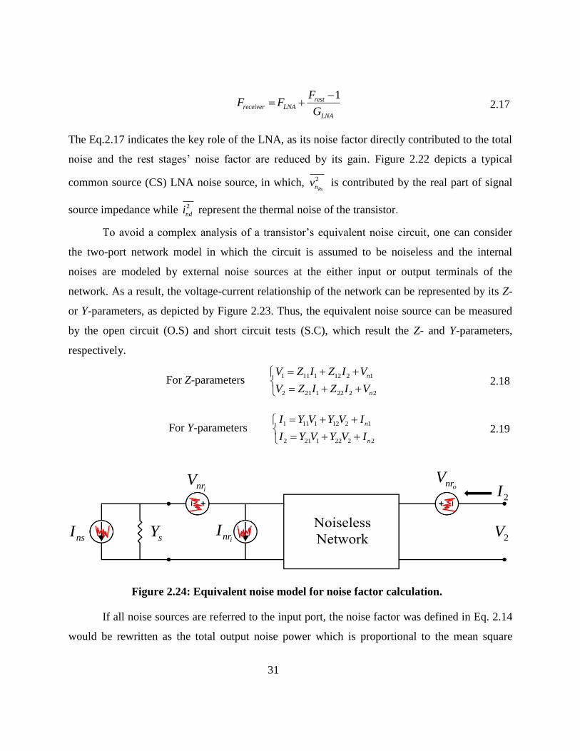
To avoid a complex analysis of a transistor’s equivalent noise circuit, one can consider
the two-port network model in which the circuit is assumed to be noiseless and the internal
noises are modeled by external noise sources at the either input or output terminals of the
network. As a result, the voltage-current relationship of the network can be represented by its Z-
or Y-parameters, as depicted by Figure 2.23. Thus, the equivalent noise source can be measured
by the open circuit (O.S) and short circuit tests (S.C), which result the Z- and Y-parameters,
respectively.
For Z-parameters 1 11 1 12 2 1
2 21 1 22 2 2
n
n
V Z I Z I V
V Z I Z I V
2.18
For Y-parameters 1 11 1 12 2 1
2 21 1 22 2 2
n
n
I Y V Y V I
I Y V Y V I
2.19
If all noise sources are referred to the input port, the noise factor was defined in Eq. 2.14
would be rewritten as the total output noise power which is proportional to the mean square
Figure 2.24: Equivalent noise model for noise factor calculation.
inrIsY 2V
2IinrVonrV
nsI

32
value of the short circuit current and the output noise power due to the input noise source
(Figure 2.24).
2.3.4 S-Parameter
As mentioned before, it is common to model LNA circuits with two-port network to
determine feature such as gain, noise, and linearity. The LNA can be characterized by its S-
parameters, which can describe the impedance matching of the circuit. Traveling waves on
transmission lines of the terminals are related to each other through the scattering (S) matrix. In
this method, the input and output signal waves will be as depicted in Figure 2.25 and can be
expressed as:
1 11 1 12 2
2 21 1 22 2
b S a S a
b S a S a
2.20
where 1a and 2a are the powers incident at the input and reflected from the load, respectively.
The 1b and 2b represent the powers which are reflected from the input port of two pole network
to the source and the output port to the load, respectively. The relation between incident and
reflection waves and voltage-current at the ports of network can be expressed as [47]:
1 11
2
o
o
V I Za
Z
2.21
Figure 2.25: S-parameter representation of Two-port noiseless network.
1V
SZ LZ
1b1a
2b2a
2V

33
2 22
2
s
s
V I Za
Z
2.22
1 11
2
o
o
V I Zb
Z
2.23
2 22
2
s
s
V I Zb
Z
2.24
The 11S and 21S are determined at the output port when it is terminated to matching load,
i.e. L oZ Z , where oZ represents the characteristic impedance. As a result, there will be no
reflection ( 2 0a ) and we have:
2
2
111
1 0
221
1 0
a
a
bS
a
bS
a
2.25
In a same manner, the 12S and 22S can be measure at the input terminal when the source
impedance is matched, S oZ Z , and we obtain:
1
1
112
2 0
221
2 0
a
a
bS
a
bS
a
2.26
In the LNA design, the input impedance must be matched with antenna impedance that usually
equals to 50 . The forward and revers voltage gain is represented by 21S and 12S , respectively,
11S and 22S are input and output voltage reflection coefficient, respectively.

34
2.3.4.1 Matching
Based on the circuit theories, to achieve the maximum power, voltage, or current
transferred in multi stage circuits, the load impedance must be appropriately designed. If the
source or load impedance are not matched with the transmission line characteristic impedance,
they will cause discontinuities in the propagation that result in reflection of a portion of the
incident signal wave. The ratio of the reflected wave to the incident wave known as reflection
coefficient and for the input and output can be expressed in terms of S-parameters as follow:
1 12 2111
1 221
Lin
L
b S SS
a S
2.27
12 21222
2 111
Sout
S
S SbS
a S
2.28
where
S oL
S o
Z Z
Z Z
2.29
L oS
L o
Z Z
Z Z
2.30
2.3.4.2 LNA gain in terms of S-parameters
The amplifier maximum power transferred is attained when input and output are complex
conjugate matched, which means *
L S and *
out in . The voltage gain, the ratio of the
output voltage to the input voltage, can be written as [48]:
212
1 22
1
1 1
L
v
L in
SVA
V S
2.31
Furthermore, the transducer gain, the ratio of the load delivered power to the source available
power, will be:

35
LT
Avs
PG
P 2.32
where
2 2
2 1L LP b 2.33
2.3.5 Nonlinearity and large signal behavior
Active elements distortion causes nonlinearities in a RF system. Therefore, in an LNA, large
input signals can change the dynamic operation point. Even in the case of small signal,
interferers may appear in the LNA input and increase the level of the operation point. According
to the Tailors’ expansion, a nonlinear system output can be expressed by:
1 2
0 1 2
1
...n
i
i
i
y a a x a x a x
2.34
where n represents the nonlinearity degree of a system. In the real world, the number of term in
Eq. 2.34 is infinity, however due to limitation of calculation; the polynomial is limited to the first
Figure 2.26: Second and third intercept point.

36
three ones. For a sinusoidal input signal of amplitude A and frequency tf , this polynomial results
in harmonic distortion of the input [36]:
32
31 20 sin 2 sin 2 sin 3
2 4 8t t t
a Aa A a Ay a f f f 2.35
Figure 2.26 depicts these harmonicas as a function of the input and output power. The slope
ration of fundamental frequency, second and third order harmonics equal to one, two, and three,
respectively. Due to nonlinearity and loss, these slopes are saturated, however, the intersections
of the extra plotted slopes between fundamental and second or third harmonic determine as
intercept point two (IP2) or three (IP3), respectively. Another challenging issue in LNA design is
the intermodulation distortion (IMD) accurse when two signals with same amplitude and small
frequency separation is presented at the input of nonlinear system, as shown in Figure 2.27. By
1f and 2f representing the input signal frequencies, second order harmonics at 12 f and 22 f and
third order harmonics at 13 f and 23 f will be produced. Furthermore, second order
intermodulation (IM2) at 1 2f f and 1 2f f as well as third order intermodulation (IM3) at
1 22 f f and 2 12 f f are generated. Considering these intermodulation terms that falls in desired
band, it’s hard to reduce them by filtering.
Figure 2.27: Fundamental and higher order products of a nonlinear system.

37
To measure the effects of intermodulation, 1-dB compression point ( 1 dBP ) is defined as
the point where there is 1dB reduction in fundamental signal at a certain frequency. As a result, it
can be approximated in terms of Taylor expression as [1]:
11
3
0.145dB
aP
a 2.36
Moreover, the input- referred IP3 (IIP3) and output-referred IP3 (OIP3) is calculated by:
1
3
43
3
aIIP
a 2.37
3 3 ( )OIP IIP Gain dB 2.38
Having OIP3 and gain value (G) of each stage of a cascade system, the total OIP3 can be
calculated as:
1 2 3 2 3 4 1
1
11
1
1 1 1 1 1...
3 3 ... 3 ... 3 3
1 1
33
tot n n n n n
n
nin
i j
j i
OIP OIP G G G OIP G G G OIP G OIP
OIPOIP G
2.39
The total IIP3 is resulted by applying above results and total gain of system to the Eq. 2.38. The
maximum to minimum input levels ratio that circuit still operates reasonable determines dynamic
Figure 2.28: The Spurious Free Dynamic Range (SFDR) demonstration.

38
range. With spurious free dynamic range (SFDR) definition, as depicted in Figure 2.28, we
obtain:
min
23 10log
3SFDR IIP NF BNL BW SNR 2.40
where BW, minSNR , and BNL represent the band width of system, the minimum SNR for a
desired signal quality, and background noise level, respectively. The BNL at the input equals to
174dBm Hz . The other expression for dynamic range is compression-free dynamic range
(CFDR) that is defined as the difference between the inputs referred 1-db compression point and
noise floor ( floorN ), in dB.
1 dB floorCFDR P N 2.41
where floorN is expressed as:
10logfloorN NF BNL BW 2.42
2.4 Optimization Techniques
In designing LNA, there are many tradeoffs between gain, NF, linearity, impedance
matching, and power consumption. To attain simultaneous noise and input matching (SNIM),
several techniques are investigated such as: classical noise matching (CNM) [2], SNIM [3],
power constrained noise optimization (PCNO) [4], and power-constrained simultaneous noise
and input matching (PCSNIM) [5, 6, 49] techniques. In the following discussion, we will report
these four LNA design optimization techniques in more details.
Figure 2.29: Equivalent input referred noise model for 2 pole network.
nisY
ne
nsi

39
2.4.1 Classical Noise Matching (CNM)
First, to simplify analysis of noise in two port network introduced in section 2.3.3, we put
all of the noise sources in the input of the noiseless network, as shown in Figure 2.29. However,
there is a problem in combining noise sources correlated with each other with varying degrees. In
the case of zero correlation between the noise powers of the source and that of the ports, the
noise figure will be as:
22
2
ns n s n
ns
i i Y vF
i
2.43
However, there are some limitations in the classical theory. First, power consumption is not
optimized in this method. Besides, the devise size for a minimum noise figure is not considered.
According to the MOSFET noise model, the mean square drain and gate current noise were
written in Eq. 2.9 and Eq. 2.11, respectively. The gate noise is correlated with the drain noise by
correlation coefficient:
*
2 2
ng nd
ng nd
i ic
i i
2.44
which its long-channel value is theoretically –j0.395 [44, 45]. To simplify the analysis, the
thermal noise due to the resistive gate is nonelected. The output noise at short-circuit noise input
port represents the equivalent input noise voltage by reflecting the drain current noise back to the
input. By neglecting channel-length modulation and assuming the ratio between the drain current
noise and its reflected value to the input as voltage noise to be mg , we will attain:
2
2 0
2 2
4nd dn
m m
i kT g fv
g g
2.45
Under open circuit condition, the value of the equivalent input current noise will be:
2 22
02
1 2 2
4nd gs d gs
n
m m
i j C kT g f j Ci
g g
2.46

40
and substituting Eq. 2.45 in Eq. 2.46:
2
2 2
1n n gsi v j C 2.47
Thus, the sum of the reflected drain noise and the induced gate current noise built the total input
current noise. In Eq. 2.47, the two ports can be correlated with each other, therefore, we can
assume ni to be the sum of two components,
ci that is correlated with nv , and
ui that is
uncorrelated with nv .
n c ui i i 2.48
ci correlation with nv will be through the admittance cY as:
c c ni Y v 2.49
Appling Eq. 2.48 and Eq. 2.49 in Eq. 2.43 results in:
2 22 2 2
2 21
ns u c s n u c s n
ns ns
i i Y Y v i Y Y vF
i i
2.50
The equivalent noise resistance/conductance of above three independent noise sources are:
2
4
nn
vR
kT f
2.51
2
4
uu
iG
kT f
2.52
2
4
nsu
iG
kT f
2.53
therefore the noise factor can be written as:
2 2
1 1u c s u u c s c s u
s s
G Y Y R G G G j B B RF
G G
2.54

41
By taking derivative of Eq. 2.54 with respects to the source admittance and setting it equals to
zero, the general condition for optimizing the noise factor is obtained as [41]:
opt s cB B B 2.55
2uopt s c
u
GG G G
R 2.56
2
min 1 2 1 2 uu opt c u c c
u
GF R G G R G G
R
2.57
Assuming the induced gate noise current to have correlated, cngi , and uncorrelated,
ungi ,
components with the drain current noise, the correlation admittance will be obtained as:
1
15
cn ng
c gs
n
i iY j C c
v
2.58
where:
0
m
d
g
g 2.59
The optimal condition for minimum noise figure will be as:
15
opt s gsB B j C c
2.60
22 15
uopt c gs
u
GG G C c
R
2.61
And finally, the minimum noise figure is approximated as:
2
min
21 2 1 1
5u opt c
T
F R G G c
2.62

42
The above approximation is exact in the case of regarding T as ratio of mg to gsC .
2.4.2 Simultaneous Noise and Input Matching (SNIM)
Shifting the optimum noise impedance optZ to desired value can be achieved through
feedback techniques [50-53]. Figure 2.30 depicts the cascade LNA including inductive source
degeneration and its small-signal equivalent circuit. A series inductor gL is applied as matching
(a)
(b)
Figure 2.30: SNIM optimization technique [3, 49].
sZ
2
nsv
2
ndigsC m gsg v
LZ
gg2
ngi
gL
sZ inZ
SL
1bV 2bV
gsv
ddV
2M

43
network and s sZ R . Adopting a similar procedure leads to the noise factor and noise
parameters as [54, 55]:
n
m
Rg
2.63
2
22
2
1 15 5
1 15 5
opt s
gs
c j c
Z sL
C c c
2.64
2
min
21 1
5 T
F c
2.65
As can be seen from the above equations, nR and minF are not changed while there is a shift in
optZ . Furthermore, the input impedance of inZ can be written as:
in
1 m ss
gs gs
g LZ sL
sC C 2.66
As a result, although inZ without degeneration does not have any real part, the source
degeneration adds real part into the input impedance. In addition, its imaginary part is shifted by
ssL . Eq. 2.66 also can be written in the form of:
2
22
2
15 1
1 15 5
opt s
gs
gs
c
Z sL msC
C c c
2.67
For a long-channel MOSFET, m is near 0.6, while with technology scaling it must be closer to 1.
To apply SNIM, following condition must be satisfied:
*
opt inZ Z 2.68
which leads to:

44
in sZ Z 2.69
opt sZ Z 2.70
in sZ Z 2.71
opt sZ Z 2.72
As Eq. 2.71 and Eq. 2.72 are the same, we can drop Eq. 2.72. In fact, the input mismatching
slightly affects the LNA operation, however, optZ directly changes the noise figure. For a given
value of sZ , the transistor size ( gsC ) can be determined by following Eq. 2.64, 2.66, and 2.70.
The value of degeneration inductor sL can be found through Eq. 2.72. finally, having gsC and
sL , the value of gsV is obtained by Eq. 2.69.
The SNIM technique allows any value of sZ by changing sL value. However, there is a
limitation in optimization for small size transistor where cause a confliction between the low
power dissiption and operation frequancy of LNA. According to Eq. 2.64, these conditions
eventutes in high optZ , and thus large sL , in which Eq. 2.65 is unvalid due to neglection of
gdC . Large sL causes the common-source gate transconductance to be degreded. In this regim,
the feedback through gdC can not be ignored any more.
2.4.3 Power-Constrained Noise Optimization (PCNO)
As mentioned previously, proper value of sL allows the satisfactions of Eq. 2.69 and 2.71 under
only conditions of power dissipation. The matching circuit of Figure 2.30 helps to reach desire
optimization with employing a series inductance gL . In power constrained technique, the
transistor size is set to the value in which the NF will be minimum, calculated as [41]:
,
1
3opt
ox s in opt
WC R Q
2.73
where:

45
, 2
5 31 1 1
5in optQ c
c
2.74
oxC accounts for gate-oxide capacitance per unit area. As a result, the minimum NF will be as
[41, 49]:
(a)
(b)
Figure 2.31: PCSNIM optimization technique [6, 49].
sZ
2
nsv
2
ndigsC m gsg v
LZ
gg2
ngi
gL
sZ inZ
SL
1bV 2bV
gsv
ddV
2M
exC

46
, 1 2.4min P
T
F
2.75
In this case, ,min PF is higher than minF of the common-source transistor, as either there is
mismatch between sZ and optZ or
sL is too large.
2.4.4 Power-Constrained Simultaneous Noise and Input Matching (PCSNIM)
Low power implementation, as an inevitable design requirement, can be attained by
inserting capacitor exC , as depicted in Figure 2.31. Adopting a similar analysis and modifying
gate induced noise current by:
2 2
2
0
45
tng eff
d
Ci kT f
g
2.76
where:
2
2
gs
eff
t
C
C 2.77
t gs exC C C 2.78
The noise parameter obtained as [49, 54, 55]:
in
1 m ss
t t
g LZ sL
sC C 2.79
n
m
Rg
2.80
2
22
2
15 5
15 5
t
gs
opt s
tgs
gs
Cc j c
CZ sL
CC c c
C
2.81

47
2
min
21 1
5 T
F c
2.82
As it is clear, inserting exC has no influence on nR and minF . These set of parameters, like SNIM
parameters, are valid for small sL . To fulfill
*
opt inZ Z , as was explained in Eq. 2.69, 2.70, 2.71,
and 2.72, we must have:
m sin s
t
g LZ Z
C 2.83
2
22
2
15
15 5
opt s
tgs
gs
c
Z Z
CC c c
C
2.84
1
s in s
t
sL Z ZsC
2.85
22
2
5
15 5
t
gs
s opt s
tgs
gs
Cj c
CsL Z Z
CC c c
C
2.86
Eq. 2.85 can be neglected since it is approximately equal to Eq. 2.86, as previously mentioned.
Therefore, we will have three equation and four unknowns: gate biasing voltage ( GSV ), transistor
size ( gsC ), addition capacitor ( exC ), and degeneration inductor ( sL ). Thus, arbitrary value of sZ
can be adopted, that leads to SNIM with any low power dissipation. Eq. 2.87, derived from
Eq. 2.83 and 2.84, verifies the fact that sL is small:
21
5s
T t
c
LC
2.87
In contrast, in SNIM technique, this value can be achieved as:

48
21
5s
T gs
c
LC
2.88
As can be inferred from Eq. 2.87 and 2.88, in PCSNIM sL is reduced by addition of exC . The
common-source LNA with an external gate-source capacitor is discussed in [6] with more
details.
(a)
(b)
Figure 2.32: Feedback and thermal noise cancellation.
fZ
SZ
SV ni
X YoV
fZ
SZ
SV ni
X Y
- vA
oV

49
2.5 Noise Cancelation Techniques
The noise signals of the circuit elements cannot be removed once they are generated.
However, they can be cancelled out each other through noise cancellation techniques. In the case
of having two nodes in which the signal is in phase and the noise is out of phase, the noise
cancellation is possible [56]. In this section, the noise cancellation techniques will be examined.
2.5.1 Active noise cancellation
By considering a noiseless two-port circuit, as depicted in Figure 2.32.a, and assuming all
the noise to be modeled as a current source, the noise cancelling method with common-source
(CS) input stage can be applied as follow [37, 56, 57]. The current merely can flows either
through fR or the source through ground. Therefore, at the point X and Y, there will be two
noise voltage having same phase but different amplification. However, the signal voltage of
these points is out of phase, as a result of an inverting amplifier between two points, and
different amplitude. To fulfill the noise cancellation condition, an inverting amplifier must be
inserted from point X. Besides, an adder will be needed as depicted in Figure 2.32.b. The
inverting amplifier’s gain can be calculated by considering the fact that the noise output voltage
must be zero that results in:
Figure 2.33: Simple implementation of thermal noise canceller with feedback.
fZ
SZ
SV
X
YoV
MainM
AuxM
BuffM
ddV

50
, 1
f
v noise
s
RA
R 2.89
Figure 2.33 shows the simple implementation of this technique with a source follower
(CS) as the negative amplifier [58-61]. Thus, the inverting amplifiers’ gain and the signal total
gain at the output will be as:
,
,
,
1f m CS
v noise
s m Buffer
R gA
R g 2.90
,
, ,
,
1m CS
v signal m Main f
m Buffer
gA g R
g 2.91
The thermal noise cancellation technique also could be applied with common-gate (CG)
input stage. This technique is well known as active balun [62]. As depicted in Figure 2.34, the
small signal current ( ini ) is equal to drain current ( dsi ) since there is no way to ground current but
through the input signal path. Therefore, the gain and input impedance can be written as:
Figure 2.34: Typical common-gate (CG) amplifier.
,L CGZ
SR
SV
oV
MainM
ddV
dcC
bVndi
ini
dsi
dcI

51
,
1in
m Main
Zg
2.92
, , ,v CG m Main L CGA g Z 2.93
On the other hand, to have high input matching:
in sZ R 2.94
Substitute Eq. 2.93 in Eq. 2.94 leads to:
(a)
(b)
Figure 2.35: Typical forward noise cancelation; (a) block diagram, (b) simple
implementation.
,L CGR
SR
SV
oV
MainM
ddV
dcC
bV,nd CGi
dcI
AuxM
oV
ddV
,L CSR

52
,
,
L CG
v CG
s
ZA
R 2.95
Considering the fact that the input and output noise voltage of CG is fully correlated with anti-
phase with each other makes this case an ideal case of main amplifier for forward thermal noise
cancelation technique which is depicted in Figure 2.35.a. Basically, the negative gain booster is
presented by a CS stage. As Figure 2.35.b depicts, the channel thermal noise current of CG stage
( ,nd CGi ) generated the following two voltages at input and output of CG stage, respectively [62].
, ,n in nd CG sv i R 2.96
, , ,n o nd CG L CGv i R 2.97
where
in
in s
Z
Z R
2.98
The Eq. 2.98 shows that is the voltage dividing ratio between the input impedance ( inZ ) and
the source ones ( sR ). The would be 1 2 in case of impedance matching at input. To make
sure that the noise of both side of balun will cancel out each other, the CS gain ( ,v CSA ) should be
equals with posit sign to the CG ones ( ,v CGA ).
,
, ,
L CG
v CS v CG
s
RA A
R 2.99
The above equivalency could be achieved by adjusting the size and load of the CS stage.
Although, this technique is improving the noise feature by cancelling the CG noise, it is still
suffering from the noise that introduced to circuit by CS amplifier. One possible solution for this
problem is the capacitor cross coupled (CCC) common gate technique which provides a
simultaneous doula way the noise cancellation for both stage [63-67]. In this configuration,
respect to the positive input, 1M works as CG amplifier. At same time, 2M plays the CS stage
role and transfers the 1M ’s reversed channel noise as well as positive input signal to the negative

53
output (Figure 2.36). The same scenario is applied to the negative input and 2M . Finally, the
differential outputs of CCC would be clear from the channel noise of both transistors.
2.5.2 Passive Noise Cancelation
The passive noise cancelation is almost following the same principal of the active ones
that was introduced in section 2.5.1. The differences between these two techniques come from
applying either passive or active balun [68, 69]. Moreover, recent publication shows that the
combination of the passive and active techniques can be count as an alternative to rich even
better noise performance [70, 71]. Figure 2.37 shows schematically the method that can be
adopted for low power and low noise figure configuration. The transformer is employed to
cancel the noise voltage created by the CG transistor drain current. As a result, there is no need
to additional negative amplifier that consumes power. Considering the noise source in
Figure 2.37, it will be found that the noise voltages ,n inv and ,n outv are generated by current
flowing, one through the sL and LR , and the other through pL and sR . The transformer
produces ,n xv having apposite phase and correlated with ,n outv , so, it can partly cancel ,n inv .
However, the high frequency power will be reduced.
Figure 2.36: Typical capacitor cross coupled (CCC) common-gate (CG) amplifier.
1LR
SR
SV
oV
1M
ddV
dcC
ndi
dcI
oV
ddV
2LR
dcC
dcC dcC
SR
SVdcI
2M

54
2.6 Non-linearity Neutralization
RF-system linearity is highly constrained by occupied narrow frequency bands and
wireless communication standards. Besides, LNA, as a first stage of a RF receiver, must be
adequately linear to avoid interferences as it deeply studied in sections 2.1 and 2.2. In addition,
LNA linearization techniques are more challenging compared with base band circuit, as they
must guarantee low noise figure, input matching, gain, and low power consumption.
Consequently, traditional linearization methods employed in low frequencies cannot be applied
for LNAs. It is worth pointing out that despite the narrowband linearization approaches, the
broadband techniques not only should improve the third- order intercept point (IIP3), but also
they must modified the second-order intercept point (IIP2) and 1dB compression point ( 1dBP ) as
well. As a result, the effect of two-tone frequency and frequency spacing on IIP2/IIP3 should be
discussed.
We can consider an LNA as a weakly nonlinear system due to the fact that the inputs are
usually high frequency and low amplitude. Therefore, its frequency-dependent distortion and the
possible compensation methods can be studied by Volterra-series analysis [73-75].
Figure 2.37: Typical passive noise canceler amplifier[72].
LZ
SZ
SV
oV
MainM
ddV
dcC
bVndi
sL
dL

55
Although CMOS technology is the first choice for on-chip circuit, there are some issues
in implementation of deep-submicron (DSM) systems such as mobility degradation, nonlinear
output conductance, poly-gate depletion, and velocity saturation [44, 46, 76]. Moreover, since
the adequate transconductance and linearity in MOSFETs need high DC current, the DC power
reduction should also be considered in LNA’s linearization techniques.
Figure 2.38 represents a weakly nonlinear amplifier without memory effects. This system
can be approximated by the first three power series term as:
2 3
1 2 3( ) ( ) ( ) ( ) ( ) Y t A X t a X t a X t a X t 2.100
where 1a , 2a , 3a denote the linear gain and second and third order nonlinearities coefficients,
respectively. If we make 2a and 3a so small that can be neglected, the term 1a will be remained
and will have:
1( ) ( )Y t a X t 2.101
The following discussion devoted to the LNA linearization methods. The main LNA
nonlinearity causes are nonlinear transconductance mg and nonlinear output conductance dsg .
The former turns the linear input voltage to nonlinear drain current, known as “input limitation”,
while the latter is swing, called also “output limitation.” Under the saturation condition and for
the frequencies under 10Tf , the CMOS parasitic capacitances, gsC , gdC , sbC , and dbC are
almost linear and bring distortion less than m dsg g . Albeit, the effect of gdC via the feedback
should be observed. The only factor involved in IIP2 is intrinsic second-order distortion,
however, the IIP3 originates from two defects: the intrinsic third-order distortion and the intrinsic
second-order distortion compounded with feedback, kwon as “second-order interaction.”
Figure 2.38: Nonlinear block.
( )A u( )X t ( )Y t

56
2.6.1 Feedback
The negative feedback circuit with a nonlinear amplifier A and linear feedback
without memory effects is schematically shown in Figure 2.39. ( )X t and ( )CLY t are the input
and output signals, respectively, fx is the feedback signal, and ex is the X and fx difference.
The third order closed-loop power series for CLY can be obtained as [77]:
2 3
1 2 3( ) ( ) ( ) ( ) ( )CL CLY t A X t b X t b X t b X t 2.102
We can derive the closed-loop linear gain 1b and second/ third-order nonlinearity 2b and 3b ,
respectively, as:
11
1 OL
ab
A
2.103
22 3
1 OL
ab
A
2.104
2
23 34
1
21
11
OL
OLOL
Aab a
a AA
2.105
Where 1OLA a denotes the linear open-loop gain. Furthermore, the IIP3 of the closed-loop
circuit and amplifier A can be attained as:
Figure 2.39: Block diagram of linear feedback with nonlinear forward block.

57
1
2,
2
IIP Amp
aA
a 2.106
21 1
3,
2 2
1IIP CL OL
b aA A
b a 2.107
1
3,
3
4
3IIP Amp
aA
a 2.108
3
1 1
3, 23 3 2
1 3
14 4
3 3 21
1
OL
IIP CL
OL
OL
Ab aA
b a Aa
a a A
2.109
As can be inferred, 2IIPA is improved by a factor of (1 )OLA in the negative feedback. In
addition, when 2 0a , 3,IIP CLA is also increased by a factor of (1 )OLA . For ordinary biasing in
which 1g and 3g is out of phase, nonzero 2g decrease IIP3. As mentioned previously, this
phenomenon cause second-order interaction [73, 78] which degrades IIP3.
However, based on the literatures, the feedback linearity modification in LNAs cannot
solve the problem since the conditions on gain, noise figure, and power consumption prevent the
open-loop gain, OLA , to be large. Moreover, the second-order non-linearity contribution in IM3
restricts the application of this technique in LNAs rather than baseband circuits. We will
investigate this technique and its issue with more details later.
2.6.2 Derivative Supersession (DS)
The derivative supersession (DS) technique is well known method for nonlinearity
cancelation. This method is widely applied in designing of LNAs and mixer in previous years
studies [79-82]. The DS technique is also known as multi gate transistor (MGT) due to its multi
transistor configurations [79]. This method is basically laid over the nonlinearity behavior of
transistor and directly works with biasing point. To explain this subject more deeply it is

58
necessary to study the effect of biasing point and feedforward effect over the transistor
nonlinearity.
2.6.2.1 Optimum Gate Biasing
As discussed before, the most effective source of nonlinear harmonics in CMOS
technology is the transconductance mg . In very simple format, the drain-source current ( dsI ) can
be expressed as follow:
d ds DS sI I i 2.110
where the first and second terms represent the DC and the AC currents, respectively The AC part
of current is a function of gate-source voltage ( gsv ). By the aim of power series, the AC term
would be:
2 3
d 2 31( )gs gss gs gsfi g g v g vv v 2.111
where 1g , 2g , and 3g are the coefficient of power series and defined as follow:
d d d1
3
2 332
21 1
, ,2! 3!
s s
gs
s
gs gsv
I I Ig g g
v v
2.112
The 1g is the linear part of the transconductance and the other coefficients are present the higher
order of nonlinear harmonics. It is essential to mention here that, although, the power series of
dsI is not finished with these three sentences, the higher order sentences are very week in term of
the power compare to the first 3 ones. By this assumption, only the characterizations of the first
three coefficients are taken into account in continues. To extract their curves as function of gate-
source voltage, first, the drain-source voltage ( DSv ) is fixed at supply voltage ( ddV ) which in this
case is 1.2V . The dsI is extracted for the gsv which is swept between 0 and ddV (Figure 2.40.a).
After all, the coefficients’ curves are available by getting first, second, and third derivation from
current ones (Figure 2.40.b, c, and d).

59
The first important point about all the Figure 2.40 is the linear behavior of these curves
versus the variation of transistor width. These figures depict the fact that the drain-source current
as well as its derivatives are linearly related to the size of transistor. We will back to this result
later.
Another important point is the sign and value of the coefficients. The 1g and 2g are
demonstrating positive sign. However, the 3g illustrates 3 different regions in its curve.
3 0g indicating the region which transistor works in deep triodes.
3 0g indicating a neighborhood which velocity saturation takes place.
3 0g indicating the strong saturation region which square low is applied.
(a) (b)
(c) (d)
Figure 2.40: NMOS current and transconductances curves.
( )dsI A
( )gsv V
1( )g A V
( )gsv V
2
2( )g A V
( )gsv V
3
3( )g A V
( )gsv V

60
Through all of these three regions, the second one is most interesting ones for harmonic
cancelation, which is also known as “moderate inversion” region [83]. One way to terminate a
specific harmonic is to decrease its amplitude in power series. The “optimum sweet spot” of IIP3
is defined as the operation point which is the zero crossing of 3g [83]. The third harmonic
products of 3
3 gsg v would be determined by adjusting the operation point near the sweet spot. This
technique is known as “optimum gate biasing” [84]. While this technique comes with a very
simple criteria, it also requires a lot of challenging conditions which counts as its draw backs.
The high sensitivity to biasing point, operation frequency, and manufacturing process are some
of it as toughest conditions. In spite of all these problems, almost same principal of optimum gate
biasing is developed in the derivative supersession.
2.6.2.2 Feedforward
To perfectly neutralize the nonlinearity of amplifier with minimum effect over the linear
coefficient ( 1g ) is demanding more degree of freedom. Usually, the second nonlinearity
coefficient is assumed to cancel out by differential configurations. Neutralization of the third
order products could be accomplished by subtracting additional nonlinear signal. This technique
is known as feedforward neutralization [85]. As illustrated in Figure 2.41, the output of the
feedforward ( TotY ) is presented by the subtracting of the outputs of main path ( MainY ) from that of
the auxiliary path ( AuxY ). The main and auxiliary paths are basically consisted of two identical
main amplifiers. In addition, the auxiliary past is involving b and 1 ( 1)n
b b scaling amplifiers
at the input and output, respectively. The n could be allocated either as 2 or 3 for canceling out
the IM2 or IM3, respectively. However, as discussed above, the neutralization IM3 is the goal of
feedforward technique. By considering all of these facts, the equation hold the relation between
the input and output will be:
2 3
2 31MainY Xg g X g X 2.113
31 2
1 2 3
2 3
Aux n n nY X
b b b
gg gX X
2.114

61
1 2
2
31 2 3
31 1 11 1 1Tot Main Aux n n n
Y Y g g X gY Xb b
Xb
2.115
Although, the third harmonic can be canceled to obtain high IIP3 by applying 3n , this
technique suffering from several problems. Due to degradation in linear coefficient (Eq. 2.115), a
reduction in linear gain is predictable. Also, as reverse relation between the noise figure ( NF )
and gain of amplifier, it would be increased as well. Furthermore, as a result of the extra active
devices, more noise would be presented to the output.
2.6.2.3 DS method
As it illustrated before, the alternative method that is resulted from combination of the
optimum gate biasing and feedforward method is derivative supersession method (DS). This
method is specific case of feedforward technique and obtained for 1b . This technique presents
a practical solution for problems which were discussed above; the short range of high value IIP3
concerned in optimum gate biasing technique and the gain reduction in feedforward technique.
The combination between feedforward and optimum gate biasing eventuate to a
noticeable expansion in zero crossing of the third order coefficient ( 3,totg ). As discussed before,
the third order coefficient ( 3g ) of drain-source current ( dsI ) is experiencing a sign change around
the optimum sweet spot due to transition between the moderate to strong inversion (Figure 2.41).
Assuming the case that the main amplifiers of the feedforward technique are replaced with two
Figure 2.41: Block diagram of feedforward linearization technique.
X Y
1 nbb
MainY
AuxY

62
MOSFETs are biased at the picks of two sides of the optimum sweet spot (Figure 2.42). When
the currents of both main and auxiliary path are added up together, the third harmonic
components are canceled out each other. Compare to the optimum biasing technique, this method
present a window of cancelation instate of a very tiny interval. The DS method takes advantages
from multiple gate connected transistors structure, it is also known as the “multiple gate
transistor technique” (MGTR) [86, 87]. In Figure 2.42, the main and auxiliary paths are utilized
by transistors AM and BM which are biased at strong inversion and moderate, respectively. The
main and auxiliary transistors represent the negative and positive peaks, respectively. Figure 2.43
depicts the maximum width of window is obtained when the positive peak is equaled to the
negative ones which is usually achieved by scaling up the auxiliary transistor compare to the
main ones.
The DS method comes with its own price. The most important issue with DS method is
its pure frequency robustness. In other words, although it provides a good degree of cancelation,
these results are just valid in low frequency. This issue rises up due to the feedback that is held
by the source degeneration inductance. As discussed previously in feedback section, the
nonlinear systems with feedback are suffered from the 2nd
-order interaction. In the DS method,
this feedback path connects the drain current ( dsI ) to the gate-source voltage ( gsv ) of the BM .
The IIP3 expression for DS method is calculated in [84] for the RF frequency with aid of
Volterra series.
Figure 2.42: Schematic demonstration of DS method.
SZ
SV
oV
MainM
MainbV
AuxMbR
dcC
SL
bR
AuxbV
dcC
oi
AuxiMaini

63
2 2
1, ,43
3
tot gs tot
Con
g LCIIP
2.116
where
2
2
,1,
,
,
3,
2
132 2
2
tot
Con tot
tot
gs tot
gs tot s
g
g j
g
C
jC Z
LL
2.117
The “tot” index in Eq. 2.116 and Eq. 2.117 is representing the total summation of the same term
of main and auxiliary transistors; for example , , ,gs tot gs Main gs AuxC C C . From Eq. 2.117, it is
obvious that the smaller Con will result the better IIP3. The first term of Con , represents the
third order coefficient which is degraded off by the DS method. The second term is product of
the feedback and indicates the 2nd-order interaction effects over IM3. This term is function of
the second order coefficient, 2,totg , and frequency. Therefore, the limitation and range of IIP3
will be determined by this term at the high frequency.
2.6.2.4 Modified Derivative Supersession Technique (MDS)
The modified derivative supersession method (MDS) was founded as on-chip solution for
2nd-order interaction in derivation supersession method (DS) [88-90]. As shown in Figure 2.44,
the MDS method was implemented with two semi-different circuits that follow same concept as
Figure 2.43: The third derivative of main and auxiliary currents.
3
3( )g A V
( )gsv V
3,Maing
3,Auxg

64
explain below. In this method, the vector of 3rd order nonlinearity contributed by the auxiliary
path ( ,3,
3
gAu s xx Aug v ) will be turned in with aid of addition phase from inductor 2L . In other words,
the angle of ,3,
3
gAu s xx Aug v is controlled through the size of this inductor (Figure 2.45). So, the
vector of ,3,
3
gAu s xx Aug v could be spilt out to the two different vectors in the opposite directions of
the 2nd-order interaction ( ,2,
2
gMa s M nin aig v ) as well as the 3rd order nonlinearity of the main path
( ,3,
3
gMa s M nin aig v ). Considering this fact, the residual part of IM3 due to the 2nd
-order interaction in
conventional DS method is eliminated now in the MDS method. The IIP3 expression for MDS
method is derived in [89] and [90]at the RF frequency by the aid of the Volterra series.
(a) (b)
Figure 2.44: Different realizations of MDS method.
(a) (b)
Figure 2.45: The distortion components (a) DS (b) MDS
SZ
SV
oV
MainM
MainbV
AuxMbR
dcC
1L
bR
AuxbV
dcC
oi
AuxiMaini
2L
SZ
SV
oV
MainM
MainbV
AuxM
bR
dcC
1LbR
AuxbV
dcC
oi
Auxi Maini
2L
el
m
3
3, ,Main gs Maing v 3
3, ,Aux gs Auxg v
2
2, ,Main gs Maing v
el
m
3
3, ,Main gs Maing v
3
3, ,Aux gs Auxg v
2
2, ,Main gs Maing v

65
2 2
1 , , 2 ,1,
,1
43
3
gs Main gs Aux gs MaMain
Mo
n
d
iI
g L C C L CIP
2.118
where
2
,1 3, 1, 1,
2,
3,
1
2 2
2
2 ,
1 , , 2 ,
1 2
,
1,
1 1
2 11
131
2
.
gs Main
gs Main gs Aux
Mod Aux Main Main
Main
Main
Main
Au
gs Main
x
g j
g
L g L g
L C g
L C C L C
L
g
Lj g
2.119
1,
2
,21
21
3( )
Main
Mod
gIIP
A j 2.120
where
, 1 2
1
2
2
1, 2 ,
1( )
( ) 1o Main
gs Aux
gs Aux
C L L
L
sA s
s g s LZ Cs
2.121
222,
,1 3, 3,
,
21
2
2
2 ,,
2( ) ( )
3 2 1
Main
Mod Main Aux
Ma
gs Aux
gs Ain ux
g g n j n jg
L Cg
L C
2.122
2
, , 1 2 1 2
2
, ,
2( ) 1 1 1gs Aux gs Aux gs Main gs Aus xo C C L LZ s s Z s s sL C L C 2.123
1,
2
1 ,
, 1 2
( )1
gs MaMa in
gs ux
n
A
iL g j
L L
j
Cn j
C
2.124
The Eq. 2.118 and 2.120 show the IIP3 expression for circuit represented in [89] and [90]
, respectively. Although, the Modified DS solve the 2nd
-order interaction problem, its drawback
should be considered carefully. Most of the difficulties of this method are referred to the
auxiliary transistor which is listed below.
Due to the large gate parasitic capacitance at week inversion and triode region, the
operating frequency should not be chosen arbitrary high.
Due to the auxiliary biasing issue, the input swing cannot be allocated the large values.

66
Due to the sensitivity of auxiliary transistor to the scaling as well as the difficulty of
matching between two transistors under the PVT variations, to catch good results, the
manual biasing adjustment is strongly recommended.
2.6.3 Noise and distortion cancelation
Distortion cancellation can be obtained using the same technique employed for noise
cancelation. The drain current of the matching device based on the Taylor approximation is
derived as [58]:
ds Main X NLI g V I 2.125
where NL depicts the high order nonlinearity terms. According to Figure 2.46, the voltage of
node X and Y can be expressed as:
X S S Main X NLV V R g V I 2.126
Figure 2.46: The IM3 neutralization presented by noise cancelation feedback method.
fZ
SZ
SV
X
Y
- vA
oV
1f 2f
1
2
2f
f
2
1
2f
f
1f 2f
1
2
2f
f
2
1
2f
f
1f 2f1
2
2f
f
2
1
2f
f
1f 2f1M

67
Y S S f Main X NLV V R R g V I 2.127
In fact, the similarity between distortion cancellation and noise cancellation comes from the
same relation between node X and Y in Eq. 2.126 and Eq. 2.127 and in noise cancellation
equations, in which, the voltage amplitude of the node Y is 1 f SR R times greater than that of
node X .
Similarly as the noise cancellation, in the distortion cancellation the feed forward gain of
1v f SA R R can cancel the matching stage’s nonlinearity terms. However, the distortion of
the noise cancellation stage will remain.
The noise and distortion cancellation technique is schematically depicted in Figure 2.46
for a CS stage. At the input, the same amplitude tones of 1f and 2f produce the 3rd
intermodulation distortion factor of 1 22 f f and 2 12 f f . As the distortion products in the node
X and Y are in phase and the fundamental signals are in anti-phase, the distortion cancellation
can be obtained by inserting a feedforward path of gin vA to the output that cancels out the
distortion products at the output. The same scenario and explanation with a little difference could
apply to active balun noise cancellation (Figure 2.35).
2.7 Summery
Just to review what was brought up in this chapter, we started from various wireless
receivers including classical and super heterodyne architectures, homodyne technology, and
ultra-low power design. Then, frequency allocation spectrum, network architecture, and
specifically WBAN application and IEEE 802.15 standardization were discussed to provide a
better context for the necessity and importance of a high gain, low noise, low weight and cost-
efficiently LNA. LNA’s gain, noise sources, noise figure and S-parameter description of its gain
were introduced in order to pave the way for argue on different noise optimization techniques
such as CNM, SNIM, PCNO, and PCSNIM. Active and passive noise cancelation techniques,
non-linearity neutralization including feedback effects and DS method were debated. In the next

68
section, these foundations will be applied to bring forward a novel LNA optimization method
and demonstrate its superiority over the aforementioned techniques.

69
Chapter 3
High Gain, Low Power, CMOS Current Reused LNA with Noise
Optimization
CMOS technology has been widely investigated in wireless communication systems due
to its compactness and low cost manufacturing [1]. The low noise amplifiers (LNA) play a
significant role in the transceiver blocks at the radio frequencies because of its improvement of
the signal to noise ratio characteristics. Upon the noise critical situation at the input transducer
systems, these families of CMOS amplifiers are reserved mainly as the first stage in the most of
the architectures. Furthermore, low cost and compactness, low power consumption, high
linearity in the pass band, and acceptable stability increase its practical importance. In order to
enhance the quality of front-end amplifiers’ operation, they should be considered as a complete
rather than a single block. That is, all of the elements included in the structure must be studied,
designed, and optimized simultaneously. Among the various possible topologies for the LNA
structures, those front end amplifiers which have CMOS inverter current reused (CICR) as their
core are outstanding owing to the wideband, high gain, and low power consumptions
characteristics. However, the complicated optimization of the CICR category has not been
analyzed yet. The published optimization techniques are mostly applied to either common source
(CS) or cascade LNAs [6, 49]. These methods, consequently, are omitting the important effects
of other noise sources, such as stacking an additional transistor; the obtained noise figure (NF) is
not optimum value. In this work, by developing and modifying the previous methods for CICR,
we achieve a more accurate procedure for stacked transistors. This chapter is organized as
follows: in Section 3.1 0 the fundamental optimization analysis technique of CICR is discussed
and Section 3.2 presents the proposed CICR optimized LNA and simulation results.

70
Figure 3.1: Flowchart of CICR Optimization.

71
3.1 Analytical Approach
To provide the essential background of CICR optimization, a theoretical procedure must
be considered preliminarily. For this reason, the optimization procedure is explained as a
flowchart (Figure 3.1). As can be seen, the first step in designing the CICR LNA is calculating
the optimal size for inverter’s transistors. This procedure leads to obtaining input impedance
matching condition. Analysis of minimum noise figure then can provide the other essential
(a)
(b)
Figure 3.2: (a) Schematic of a CICR LNA, (b) Small signal equivalent circuit with noise
sources.

72
criteria for LNA’s optimization. The Figure 3.2 depicts the schematic of a CICR LNA and its
equivalent small circuit model including channel thermal noise sources ( 2
nndi and 2
pndi ), the gate
induced noise sources ( 2
nngi and 2
pngi ), determined by Eqs. 2.9 and 2.10, respectively. The
correlation coefficient (c) of the channel thermal and gate induced noise sources were defined as
Eq. 2.44. In the suggested mathematical approach, the transistors’ size, degeneration inductors
( SL ), and gate source compensator capacitors (NaC and
PaC ) values are estimated.
3.1.1.1 Transistors’ Size and CICR gain
Calculating the size of transistor in CMOS inverter offers an assumption that simplifies
the complicated relationship between noise parameters and circuit elements, therefore, serves as
an essential requirement to establish the final practical formulas. The drain current ( DSI ) and
drain-source saturation voltage (NDsatV ) of NMOS are given in Eqs. 3.1 and 3.2 , respectively
[46].
2
2 1
N
N
N
N oxDS OD
NOD
C N
C WI V
LV
L
3.1
2
1 1N
N N
N
OD
Dsat C N
C N
VV L
L
3.2
where W and L are the channel width and length, respectively. oxC is the gate oxide capacitance
per unit area, and it is related to the oxide thickness oxT by ox ox oxC T . NODV is the overdrive
voltage and equals to OD GS thV V V . After some manipulations one obtains:
2
222 2
N
NN N N N
ODN oxDS
N DsatDsat ot OD Dsat
VC WI
L VV V V V
3.3

73
Table 3.1: Technology dependent variables’ value.
Variable Mean Value
Total = 2.5 = 2.7 = 3
NC NL 0.2654 0.2711 0.2661 0.2589
PC PL 1.3926 1.4035 1.3937 1.3805
2N ox
N
CL
3363.0 3236.1 3351.3 3501.5
2P ox
P
CL
748.45 779.4750 754.2721 717.5927
NDsatV 0.1404 0.1397 0.1403 0.1411
PDsatV 0.2024 0.2024 0.2024 0.2024
NthV 0.4224 0.4242 0.4226 0.4204
PthV 0.4123 0.4122 0.4123 0.4124
N
P
m
m
g
g 1.0362 1.0630 1.0391 1.0065
NgsC fF 48.010 47.997 48.009 48.024
PgsC fF 116.99 106.69 115.56 128.42
NgdC fF 16.481 16.539 16.496 16.409
PgdC fF 42.851 38.404 42.223 47.927
N
N
gs
gd
C
C 2.9145 2.9033 2.9118 2.9285
P
P
gs
gd
C
C 2.7299 2.7791 2.7336 2.6770
P
N
gs
gs
C
C 2.4355 2.2279 2.4056 2.6729

74
Since both transistors operate at saturation region with the same current (N PDS SDI I ), equal
biasing voltage ( 2N Pgs sg DDV V V ), and the drain current ( DSI ) and drain-source of NMOS is
given in Eq. 3.3, the inverter ratio would be defined as in Eq. 3.4.
2 2 2
2 22
2
2
N P P P N N
P PN N N N
Dsat ot OD Dsat Dsat ODP P
N N Dsat ODDsat ot OD Dsat
V V V V V VW
W V VV V V V
3.4
Due to the fact that the calculations of technology dependent constants lead to inaccurate values,
we utilized the simulator’s features to gain more precise values. Table 3.1 provides th details
about the technology dependent variables which are required for the optimization numerical
calculations. As a result, the optimum value of 2.7 for the ratio is attained by extracting the ODV
and DsatV directly from the simulator. In the best ratio NMOS and PMOS transistors operate
almost equally in term of amplification and possess the same transconductance as in Eq. 3.5.
2
12
n n P
p n p
m DS OD
m OD SD
g I V
g V I 3.5
Figure 3.3: The CICR’s forward gain in low frequency versus the ratio of inverter.

75
In determining the channel capacitances, gsC , we should consider that if the thickness of oxide is
assumed to be equaled for both of the PMOS and NMOS ( N Pox oxT T ), the below equation could
be driven:
2
3
2
3
N
P
N
P
gs ox Ngs P
gs Ngs ox P
C C WLC W
C WC C WL
3.6
Based on the assumptions and the equivalent circuit of Figure 3.2.b, the low frequency voltage
gain is obtained as:
n p
ov m o o
in
VA g r r
V 3.7
where mg equals to summation of Nmg and
Pmg . The relevance between the CICR’s forward
gain and the ratio of transistors is illustrated in Figure 3.3. It proves that that the ,maxvA occurs at
calculated ratio from Eq. 3.4. In addition, the gain curves are extracted for a wide range of
transistors’ width. These results demonstrate the independency of optimum to the size of the
transistors. The input impedance of CICR can be expressed as:
||n pin in inZ Z Z 3.8
where ninZ and
pinZ represent the input impedance of NMOS and PMOS transistors,
respectively.
1
n
n
m s
in s
tot tot
g LZ L s
C s C 3.9
1
1 1
p
p
m s
in s
tot tot
g LZ L s
C s C
3.10
totC is the accumulation of the gate–source’s parallel capacitors (n p n ptot gs gs a aC C C C C ).

76
1p ptot gs aC C C 3.11
n ntot gs aC C C 3.12
naC and paC represent the gate-source compensator capacitors for NMOS and PMOS transistors,
respectively. The is the proportion ratio constant and 0< <1 . In order to have better matching
at input and decrease the input reflection ( 11S ), the inZ can be minimized one step before starting
actual optimization which is one of the advantage of this method. To do so, we can adjust .
The size of capacitors and inductors is lifted as freedom for the noise optimization calculations.
Therefore, the optimum inZ is achieved by 1 2 . By substituting this condition and Eq. 3.5
into the Eq. 3.8, we have:
1
2
nm ssin
tot tot
g LL sZ
C s C 3.13
The new condition guarantees the equivalency of input impedance of both transistors.
3.1.1.2 Noise Parameters
From the Eq. 2.43, the noise factor of CICR LNA can be described as:
22
2
n pns rn ng ng s rn
ns
i i i i Y vF
i
3.14
where 2
nri and 2
nrv are the power of input referred noise as current and voltage which obtained
from the open and short circuit analysis, respectively. The 2
nsi is attributed to the thermal noise of
the source resistance sR and sY represent source admittance. The referred noise as voltage
source to the input of a CS amplifier with degeneration inductor is calculated from the short
input test which results:

77
, 1
2 22 2
(1 )n SC
d oo nd
d o S m o
R rv i
R r L s g r
3.15
In case a voltage noise source is available at input, the output would be:
1
2 22 2 2
(1 )n
d oo m n
d o S m o
R rv g v
R r L s g r
3.16
Now, putting the Eq. 3.14 equals to Eq. 3.15 result in the input referred noise as voltage.
, 1 1
2 2 2 2
2
1n SC no o n nd
m
v v v ig
3.17
The procedure of attaining the referred noise as current source is similar to the voltage ones
except the open circuit at input instead of short circuit test.
, 2
22 2
n OCo o S ndv r sL i 3.18
In case of a current noise source is available at input, the output would be:
2 1
2 2
2 2
2 2n
o S m
o n
gs
r sL gv i
C 3.19
Comparing the Eq. 3.18 and Eq. 3.19 results in the input referred noise as current.
1
22 2
2 2
mnd n
gs
gi i
C 3.20
Based on the assumption in previous section, the Eq. 3.17 and Eq. 3.20 can be extended and
applied to CICR LNA. Therefore:
2 2 2
2
1n prn nd nd
m
v i ig
3.21
2 2
2 2 2 2 2 2
2 n p
totrn tot rn nd nd
m
Ci C v i i
g
3.22
By considering the traditional equivalent noise resistance (Eq. 2.51), the rnR is attained as:

78
2 22
2
0 0 0 0
2 2
1
4 4
(4 4 ) ( )
( ) ( )
n p
n p n p
n p n p
nd ndrn
rn
m
d d d d
m m m m
i ivR
kT f kT f g
kT g f kT g f g g
g g g g
3.23
In the week inversion we have:
00 1pn
n p
dd
m m
gg
g g 3.24
where the constant of is defined as 0d mg g , and equals to 1 for long channel devices, and it is
same for both NMOS and PMOS transistors. The channel scaling down directly decreases the
. For any sets of 4 real number which:
a c
b d 3.25
the following equality is given
a c a c
b d b d
3.26
Substituting Eq. 3.24 and Eq. 3.26 in Eq. 3.23 results:
0 0( )
( )
n p
n p
d d
rn
m m m m
g gR
g g g g
3.27
The correlation admittance, TcY , can be expressed as:
n p n p
T
n p
rn ngc ngc ngc ngc
c tot m
rn nd nd
i i i i iY j C g
v i i
3.28
In order to apply more simplification to the TcY , the correlation relation between noise sources
should be considered precisely.
79
1
1
n p n p n p pn
n p n p n n p p
n n p n n p p p
n n p n n p p p
ngc ngc ngc ngc ngc ngc ndnd
nd nd nd nd nd nd nd nd
ngc nd ngc nd ngc nd ngc nd
nd nd nd nd nd nd nd nd
i i i i i i ii
i i i i i i i i
i i i i i i i i
i i i i i i i i
3.29
The correlation between all the possible pairs of CICR’s noise sources is zero except those that
belong to the same transistor (Eq. 20).
, 0 , 0
, 0 , 0
, ,
n p n p
n p p n
n n p p
nd nd ng ng
ng nd ng nd
ng nd ng nd
Corr i i and Corr i i
Corr i i and Corr i i
Corr i i c and Corr i i c
3.30
By applying Eq. 3.30 to Eq. 3.29, we have:
00
10 0
n p p pn n
n p n n p p
ngc ngc ngc ndngc nd
nd nd nd nd nd nd
i i i ii i
i i i i i i
3.31
which can be rewrite as:
2 2
22
2 22 2
1
1
n p p pn n
n p n p
pp pnn n
n pn p
ngc ngc ng ndng nd
nd nd nd nd
ngng ndngng nd
nd ndng ng
i i i ii i
i i i i
ii iii i
i ii i
3.32
More simplification will be done by substituting Eq. 2.44 in Eq. 3.32:
0 0
2 22 2
2 21
5 5
n p pn
d d pn p n
ngc ngc gsgs
nd nd
i i CCc c
g gi i
3.33
where is the constant and equals to 1 2 . Thus, Eq. 3.28 will be:
80
0 15
n p
T
gs gs
c tot
tot
C CY j C c
C
3.34
By considering the basic explanation for the equivalent noise conductance (Eq. 2.52 ), the total
uncorrelated conductance (TuG ) is calculated as follow:
2 22 2 2 2 2 2 2 1n p n p n png ng ng ng ng ng ngi i i i i c i i c 3.35
which the second term represents the un-correlated part of gate noise ( 2
ngui ).
0 0
22 22
2222
1
4 4
15
n p
T
pn
T
d n d p
ng ngngu
u
gsgs
u
i i ciG
kT f kT f
CCG c
g g
3.36
Based on the details that provided in Table 3.1 and the relation between ngsC and
pgsC , it can be
concluded:
2
2 22n p n pgs gs gs gsC C C C for 2 3 3.37
Substituting Eq. 3.37 into Eq. 3.36, we have:
0 0
2
22
15
n p
T
d n d p
gs gs
u
C CG c
g g
3.38
According to the above results one can rewrite Eq. 3.14 as:
2
1 T Tu c s rn
s
G Y Y RF
Y
3.39

81
3.1.1.3 Minimum Noise Figure
Based on the parameters derived in previous sections and Eq. 2.62, the minimum noise
figure of CICR can be attained as:
2
min 1 2 1 1 15
rn opt
T
F R G c
3.40
where:
0.5
25 1
n popt gs gsG c C C
3.41
As a result, optZ is found to be:
2
1*
22
2
15 51
1
15 5
n p
T
n
n p
tot
gs gs
opt opt c
gstot
gs gs
Cc j c
C CZ G Y
CC
c cC C
3.42
Based on the section 2.4.4 discussions, the optimization condition, *
opt inZ Z , require to observe:
Rel Relopt inZ Z 3.43
After some calculation one obtains:
22 1 1
5ngs
s tot
m
C c
L Cg
3.44
As discussed in chapter 2, Eq. 3.44 represents the essential condition for designing optimum
LNA. In the next section, this criteria is applied for the designing the CICR LNA.
82
3.2 Simulation and Discussion
3.2.1 Noise Figure and Transistor’s Size
Considering the fact that no analytical procedure could reasonably approximate the
optimum value for transistor size and number of fingers, in this part we deduce their values
through numerical investigation. Figure 3.4.a demonstrates that NMOS optimum size should be
14.5µm. Despite of common belief, the multi-fingered transistors demonstrate better NF than a
single transistor with the same equal width. Figure 3.4.b indicates that by increasing the number
of fingers per transistor to 4, NF is significantly decreased. Figure 3.4.b depicts the optimum
transistor size and number of fingers for each of NMOS and PMOS can be derived. It is
necessary to remind that number of fingers for PMOS should be extracted from NMOS ones by
applying the ratio factor.
The next point is the value of biasing voltage. As mentioned in Section I, the gate voltage
of transistors should be pulled up to 2ddV , due to the equivalency considered for inverter pair at
the optimum ratio. Figure 3.4.c illustrates both the minNF and ,maxvA can be achieved when bV
equals to 0.6 V for the ratio between 2 to 3.
3.2.1.1 CICR’s Optimized Noise Figure
By utilizing the optimum values obtained in Section 0 3.1, both sL and totC are found by
Eq. 3.44. The operation frequency is 2.4GHz which is intended for WBAN applications.
Figure 3.5.a depicts the NF and forward gain variations with sL , in different totC . It can be
inferred from the plots, minNF occurs at higher sL and lower totC , indicated by dashed line.
However, as the source inductors cannot take arbitrary large values due to the area limitation, we
restrict it to 10nH. Therefore, the size of compensator capacitances will be found by substituting
the sL value in Eq. 3.44. Figure 3.5.b depicts that the optimum totC value is adequately close to
the designed one. This small mismatching is caused by the primary assumption that neglects the
drain-source parasitic capacitances.

83
(a) (b)
(c)
Figure 3.4: Variation of vA and NF as function of: (a) transistor width, (b) number of
fingers, (c) DC biasing.
()
vA
dB
()
NF
dB
( )bV V

84
This set of parameters’ values result in 1.69dB for NF, 27dB for vA , and -9.14dB for 11S .
To improve these values that are extracted without employing any matching network, we suggest
a very small L matching at the LNA input. Therefore, this design will be more compact
compared with the previous ones that utilized the gate inductor ( gL ). Using this approach, 11S
and vA improve to -18.6dB and 28, respectively, although NF increases to 2.46dB (Figure 3.6.a).
Figure 3.6.b represents the third-order intercept point (IIP3) of LNA which is equal to -10.1
dBm.
3.2.1.2 Process, Power Supply, and Temperature Variation Monitoring
To clarify the reliability of our optimization method and guarantee fabrication of
designed CICR LNA, the process, supply voltage, and temperature (PVT) variation monitoring
was applied. The test were done within 45 different states, which include all the five possible
(a) (b)
Figure 3.5: Variation of vA and NF as function of: (a) degeneration inductors, (b)
compensation capacitors.

85
CMOS process variations (ff, fs, sf, ss, and tt), 10 fluctuation in power supply, and
temperature variation between -27 to 100 C (Figure 3.7). The PVT test results are shown in
Table 3.2, reveal that the designed LNA insignificantly affected which indicated robustness of
this design to the PVT variation. Besides, as depicted in Figure 3.7, the proposed LNA based on
the CICR optimization method is always tracking the best possible gain, NF, and input matching.
In other words, the optimization provides a mechanism which the best achievable performance of
design at the desirable frequency.
Table 3.2: PVT Test Result at 2.4 GHz
Av (dB) NF (dB)
Min 25.9 1.93
Max 28.5 3.27
3.3 Summery
To summarize, this chapter sparked off a novel technique of LNA noise optimization by
introducing a CMOC inverter current reused architecture and suggested a powerful mathematical
(a) (b)
Figure 3.6: CICR LNA with L matching at input results: (a) Forward gain, Noise
Figure, and input reflection, (b) third-order intercept point (IIP3).

86
foundation that excelled from all previous ones at precise prediction and achievements. A huge
load of calculation, eight times greater than the precedent methods which all focused on one
transistor optimization, was required to take to account all the noise sources, including the both
transistors at the same time in addition to their sizes’ ratio. This mainly is due to the fact that all
the parameters such as gain, input matching, and power are associated with the transistors width’
ratio. Besides, there are two inductors and two capacitors to be optimized which are twice the
numbers of elements in the preceding techniques. Considering all together, it can be conclude
that the difficulty and the amount of the computations of the presented method will be about
eight times compared to the former ones like PCSNIM. As a result, we could achieve the LNA
design with as high gain as 27dB, as well as a low noise figure of 1.69dB. The analytical
procedure included determining the transistor size, noise parameters, and minimum noise figure
are fully discussed in this chapter and the multifaceted simulation results completely elaborates
the performance.
(a) (b)
(c)
Figure 3.7: PVT test results, (a) voltage gain, (b) noise figure, (c) input matching (S11).
87
Chapter 4
Feedback and Nonlinearity
4.1 Introduction
The input to output transfer function of a circuit with the linear elements and feedbacks
could be simply presented based on the linear feedback theory. This method covers the circuit
with the memory effect. It is also applicable for the circuit with the first degree of nonlinearity
effects. As it discussed in Section 2.6.1, the power series should be employed for this case with
some assumptions. However, in the case of circuits with third and higher nonlinearity effects as
well as the memory ones this method sounds ineffective. Thus, it’s required an alternative means
for this type of calculations: The Volterra nonlinear elements, memory effects, and feedbacks
[73]. Working with multi excitations’ input is the most significant point about the Volterra series.
In other words, the Volterra kernels which is also known as the multi-dimensional Fourier
transfer function give us opportunity to work with multi tones input as well as the produced
intermodulation (IM) terms.
This chapter will mostly discuss around the nonlinear effects over the circuit with
negative feedback and memory effects. While Section 4.2 is assigned to Volterra series
calculation, an extensive comparison between these results and power series’ ones is presented in
Section 0. To keep the simplicity of this chapter and reduce the weight of mathematical
equations, a well-organized tutorial for Volterra series is presented at Appendix A.
4.2 Nonlinear Analyses of Feedback
Based on the proposed steps in Appendix A (Figure A.2), Figure 4.1 depicts the block
diagram of typical CMOS LNA with the negative feedback. The backward block, ( ) ,
represents a feedback with memory effects. It’s usually presented in term of either a band pass
(BPF) or high pass (HPF) filter. The main transistor, MainM , is modeled by forward block, while
( )f u represents the nonlinearity behaviors of its transconductance.

88
2
1 2
1
( ) ...f
f
f
f
Nmn
n m
m
f u g u g u g u g u
4.1
where ig represents the ith-order derivative of drain-source current which widely discussed in
Section 2.6.2. For the CS LNA circuit, ( )x t and ( )y t identify the input voltage and output
current and are defined by Eq. A.3 and A.5, respectively. In this manner, the source voltage and
gate-source one is specified by ( )fx t and ( )ex t , respectively, and are defined as follow:
( ) ( ) ( )fx t y t 4.2
(a)
(b)
Figure 4.1: Typical CMOS LNA with negative feedback: (a) schematics’ presentation,
(b) equivalent block diagram.

89
( ) ( ) ( )e fx t x t x t 4.3
Substituting Eq. 4.2 and 4.3 in Eq. 4.1, we have:
1
( ) ( ) ( ) ( )f
f
f
f
Nm
m
m
y t g x t y t
4.4
Up to this point, the mathematical relation between the input and output has been
formulated from the block diagram of circuit. The Volterra kernels will be calculated in the next
steps.
4.2.1 Volterra kernels
Considering the output formula, the volterra kernels could be extracted from Eq. A.11
and A.12 when the circuit is excited by a single frequency, 1 .
1 1
1
1
1
1
1( ) exp( ) exp( )
2q q
q
x t X j t j t
4.5
Applying Eq. A.5 and 4.5 into Eq. 4.4 and eliminating the higher order terms, we would have:
0
1
2
( ) ( )N
n
n
y t y t
1 1
2
( ) ( ) ( ) ( )N
n
n
g x t y t y t
0
2
( ) ( ) ( )f
f
f
f
Nm
m
m
g x t y t
0
4.6
1 1 1( ) ( ) ( ) ( )y t g x t y t 4.7
Eq. 4.7 represents the linear case of the circuit. Thus, the first kernel is extracted by applying Eq.
A.10 into Eq. 4.7 as:
1 1 1 1 1 1 1
1 1
1 1
1 1 1 1
1 1
1 1( )exp( ) exp( ) ( ) ( )exp( )
2 2q q q q q q q
q q
X H j t g j t X H j t
11 1
1 1
( )1 ( )
gH
g
4.8

90
After calculation of the first order term, the second order kernel calculation could be started by
increasing the number of excitations to two tones ( 1 2, ).
1 1
1
2
1 2
1
1( ) exp( ) exp( ) exp( )
2q q
q
x t X j t j t j t
4.9
Similar to the first order calculations, substituting Eq. A.5 and 4.9 into the circuit input to output
function will result in:
1( )y t
00
2
3
( ) ( )N
n
n
y t y t
1 ( )g x t
0
1( ) ( )y t
0
2
2
( ) ( )N
n
n
y t y t
0
2 1
2
( ) ( ) ( ) ( )N
n
n
g x t y t y t
20
3
( ) ( ) ( )f
f
f
f
Nm
m
m
g x t y t
0 4.10
22
2 1 2 2 1 2 1( ) 1 ( ) ( ) 2 ( ) ( ) ( ) ( ) ( )y t g g x t g x t y t g y t 4.11
The Eq. 4.11 demonstrates only the terms which includes the second order harmonics. However,
it still needs more purification in order to extract the exact terms which are function of just two
different input tones. In the light of this statement, the terms in Eq. 4.11 are rewritten as follow:
1 2 1 2 1 2 1 2
1 2
1 1 2 2
1 2
1 1 2 2 2 2
1 2
1
2 2
1 221 1
2 2
2
1 1
2 2
2 1
1 1
2
11 ( ) ( , ) exp ( )
2
1 1exp( ) exp( )
2 2
1 12 exp( ) ( ) ( ) exp( )
2 2
1(
2
q q q q q q q q
q q
q q q q
q q
q q q q q q
q q
q
X X g H j t
g X j t X j t
g X j t X H j t
g X
1 1 1 2 2 2
1 2
2 2
1 2 1
1 1
1) ( )exp( ) ( ) ( ) exp( )
2q q q q q q q
q q
H j t X H j t
4.12
Applying the summations’ order interchange methodology results in:

91
1 2 1 2 1 2
1 2
1 2 2 2 1 2
1 2 1 2
1 1 2 2 1 2
1 2
2 2
1 2
1 1
2 2 2 2
2 2 1
1 1 1 1
2 2
2 1 1
1 1
1 ( ) ( , ) exp ( )
exp ( ) 2 ( ) ( ) exp ( )
( ) ( ) ( ) ( ) exp ( )
q q q q q q
q q
q q q q q q
q q q q
q q q q q q
q q
g H j t
g j t g H j t
g H H j t
4.13
By extracting the terms which includes 1 and 2 simultaneously we would have:
1 1 2 2 1 2 2 2 1 1 1 2 1 2
2 1 1 1 2 1 2
2 1 ( ) ( , ) 2 2 ( ) ( ) ( ) ( )
2 ( ) ( ) ( ) ( )
g H g g H H
g H H
4.14
2 1 1 1 2 1 2 1 1 1 2 1 2
2 1 2
1 1 2
1 ( ) ( ) ( ) ( ) ( ) ( ) ( ) ( )( , )
1 ( )
g H H H HH
g
4.15
The Eq. 4.15 could be more simplified by substituting Eq. 4.8:
22 1 2
1 1 2 1 1 1 2
( , )1 ( ) 1 ( ) 1 ( )
gH
g g g
4.16
So far, the first and second kernels are calculated. As recursive flowchart (Figure A.2) indicates,
all the essentials for the third order transfer function computation are provided.
1 1
1
3
1 2 3
1
1( ) exp( ) exp( ) exp( ) exp( )
2q q
q
x t X j t j t j t j t
4.17
Hence, exciting circuit by three different tones (Eq. 4.17) and apply it to Eq. A.12 will result in:
3( ) ...y t
0
1 ( )a x t
0
3( ) ( ) ...y t
0
2 1 2( ) ( ) ( ) ( ) ...a x t y t y t
20
3 1( ) ( ) ( ) ...a x t y t
30
...
0
4.18
Simplifying Eq. 4.18 and extracting only the third order terms yields:
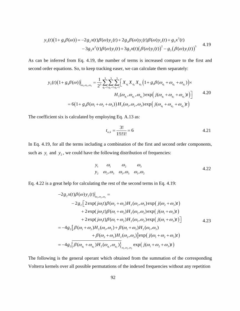
92
3
3 1 2 2 2 1 2 3
2 32
3 1 3 1 3 1
( ) 1 ( ) 2 ( ) ( ) ( ) 2 ( ) ( ) ( ) ( ) ( )
3 ( ) ( ) ( ) 3 ( ) ( ) ( ) ( ) ( )
y t g g x t y t g y t y t g x t
g x t y t g x t y t g y t
4.19
As can be inferred from Eq. 4.19, the number of terms is increased compare to the first and
second order equations. So, to keep tracking easer, we can calculate them separately:
1 2 3 1 2 31 2 3
1 2 3
1 2 3 1 2 3
1 2 3
3 3 3
3 1 13, ,1 1 1
3
1 1 2 3 3 1 2 3
1( ) 1 ( ) 1 ( )
2
( , , ) exp ( )
6 1 ( ) ( , , ) exp ( )
q q q q q q
q q q
q q q q q q
q q q
y t g X X X g
H j t
g H j t
4.20
The coefficient six is calculated by employing Eq. A.13 as:
,
3!6
1!1!1!n kt 4.21
In Eq. 4.19, for all the terms including a combination of the first and second order components,
such as 1y and 2y , we could have the following distribution of frequencies:
1 1 2 3
2 2 3 1 3 1 2, , ,
y
y
4.22
Eq. 4.22 is a great help for calculating the rest of the second terms in Eq. 4.19:
1 2 32 2 , ,
2 1 2 3 2 2 3 2 3
2 1 3 2 1 3 1 3
3 1 2 2 1 2 1 3
2 1 2 2 1 2 1 3 2 1 3
2
2 ( ) ( ) ( )
2 2exp( ) ( ) ( , ) exp ( )
2exp( ) ( ) ( , ) exp ( )
2exp( ) ( ) ( , ) exp ( )
4 ( ) ( , ) ( ) ( , )
(
g x t y t
g j t H j t
j t H j t
j t H j t
g H H
1 2 1 2
1 2 3
3 2 2 3 1 2 3
2 2 1 2 3, ,
) ( , ) exp ( )
4 ( ) ( , ) exp ( )q q q q
H j t
g H j t
4.23
The following is the general operant which obtained from the summation of the corresponding
Volterra kernels over all possible permutations of the indexed frequencies without any repetition

93
of output terms:
1 2 31 2 3
1 2, ,
1 1 2 2 3 1 2 2 1 3 1 3 2 1 2
( ) ( , )
( ) ( , ) ( ) ( , ) ( ) ( , )
q q qX X
X X X X X X
4.24
Applying a same approach to the rest of the terms, we will have:
1 2 32 1 2 , ,
2 1 1 1 1 2 3 2 2 3 2 3
2 1 2 2 1 3 2 1 3 1 3
3 1 3 3 1 2 2 1 2 1 2
2 1 1
2 ( ) ( ) ( ) ( )
2 2 ( ) ( ) exp( ) ( ) ( , ) exp ( )
2 ( ) ( ) exp( ) ( ) ( , ) exp ( )
2 ( ) ( ) exp( ) ( ) ( , ) exp ( )
4 ( )
g y t y t
g H j t H j t
H j t H j t
H j t H j t
g H
1 1 2 3 2 3
1 2 3
1 1 2 2 1 2 2 1 2 1 3 2 1 3
3 1 3 2 3 2 2 3 1 2 3
2 1 2 1 2 3, ,
( ) ( ) ( , ) ( ) ( ) ( ) ( , )
( ) ( ) ( ) ( , ) exp ( )
4 ( ) ( ) ( ) ( , ) exp ( )q q q q q q
H H H
H H j t
g H H j t
4.25
1 2 3
2
3 1 , ,
3 1 2 3 1 3 3
1 3 2 1 2 2
2 3 1 1 1 1
3 1 1 1 2 1 2 3 1 3 1 2 3
3
3 ( ) ( ) ( )
3 2exp ( ) ( ) ( ) exp( )
2exp ( ) ( ) ( ) exp( )
2exp ( ) ( ) ( ) exp( )
6 ( ) ( ) ( ) ( ) ( ) ( ) exp ( )
6 ( q
g x t y t
g j t H j t
j t H j t
j t H j t
g H H H j t
g
1 1
1 2 31 1 2 3
, ,) ( ) exp ( )qH j t
4.26
1 2 3
2
3 1, ,
3 1 2 1 2 3 1 3 2 3
2 1 1 1 3 1 3 1 3
3 1 1 1 2 1 2 1 2
3 1 1 1 2 1 2 1
3 ( ) ( ) ( )
3 2exp( ) ( ) ( ) ( ) ( ) exp ( )
2exp( ) ( ) ( ) ( ) ( ) exp ( )
2exp( ) ( ) ( ) ( ) ( ) exp ( )
6 ( ) ( ) ( ) ( ) ( )
a x t y t
g j t H H j t
j t H H j t
j t H H j t
g H H
1 1 2 2
1 2 3
1 1 3 1 3
2 1 2 3 1 3 1 2 3
3 1 1 1 2 3, ,
( ) ( ) ( )
( ) ( ) ( ) ( ) exp ( )
6 ( ) ( ) ( ) ( ) exp ( )q q q q
H H
H H j t
g H H j t
4.27

94
1 2 3
3
3 3 1 2 3, ,( ) 6 exp ( )g x t g j t
4.28
1 2 3
3
3 1, ,
3 1 2 3 1 1 1 2 1 3 1 2 3
( ) ( )
6 ( ) ( ) ( ) ( ) ( ) ( )exp ( )
g y t
g H H H j t
4.29
Substituting Eq. 4.20, 4.23, and 4.25- 4.29 into Eq. 4.19 results in:
1 2 1 21 2 3
1 1 2 3 2 3 1 11 2 31 2 3
1 1 2 21 2 3
3 1 2 3 2 2, ,
1 1 2 3
1 2 3 1, ,, ,
1 1 1 2 3 1 1, ,
1( , , ) 4 ( ) ( , )
6 1 ( )
( ) ( ) ( ) ( , ) 6 1 ( ) ( )
( ) ( ) ( ) ( ) ( ) ( ) ( ) ( )
q q q q
q q q q q q q q
q q q q
H g Hg
H H g H
H H H
1 2 1 3( ) ( )H H
4.30
By calculating the third Volterra kernel, 3H , the most of the materials required for IIP3
calculation is collected. The final step is reminded is to reconfigure and apply them to IIP3
equation which would be the subject of the next section.
4.2.2 IIP3
As discussed in Appendix A, for IIP3 calculation, we have to prepare the Volterra kernels
to be acceptable by Eq. A.20. Having this attitude, first 3( , , )H should be provided which
in turn requires the calculation of 1( )H , 1( )H , 2 ( , )H , and 2( , )H . Before
continuing these computations, it is helpful to consider an important assumption of:
( ) ( ) 4.31
Applying this assumption, the volterra kernels for those specific pairs of frequencies would be:
11
1
( )1 ( )
gH
g
4.32
11
1
( )1 ( )
gH
g
4.33

95
22 2
1 1
( , )1 (2 ) 1 ( )
gH
g g
4.34
22 2 2
1 1
( , )1 (0) 1 ( )
gH
g g
4.35
2
2 3
3
( )( , , )
( )
( )
f f
f
Ag gH
B
C
4.36
where:
1 1 1( ) ( ) (0( ) 2 2 2 1 2 2 2 1) ( ) ( )f g g gA 4.37
2 2
1 1 1 1( ) 3 1 1 2 1(0) ( ) (2 3) ( )1fB g g g g 4.38
1 1 1 1
3( )( ) 3 1 1 1 1( 2) (0) ( )f g gC g g 4.39
Substituting 1( )H and 3( , , )H in Eq. A.20 yields:
1
2
1 2 3
( )43
3 1) ( ) ( )(
f
f f
CIIP
A g B
g
g g
4.40
Eq. 4.40 shows the IIP3 of the circuit with nonlinear forward gain and feedback with memory
effects. We will elaborate to this point later.
4.3 Power series vs. Volterra Series
In Section 2.6.1, the close loop gain of nonlinear amplifier with negative feedback had
been discussed. However, as it was mentioned, the equation does not take care of the memory
effects. The aim of this section is investigating the Volterra series results versus the power series’
ones for the same circuit. This comparison will prove the accuracy of this method. Furthermore,
it would shows the comprehensiveness of this series when we have to deal with a nonlinear
circuit with the memory and feedback effects. Therefore, to start, the memory effects will be
removed from Figure 4.1.b which will transform it to the Figure 2.39. To apply this change to the
Volterra kernels and IIP3, the memory effects have to be removed from the equations as follow:
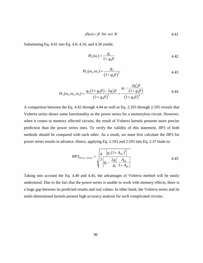
96
( ) for 4.41
Substituting Eq. 4.41 into Eq. 4.8, 4.16, and 4.30 yields:
11 1
1
( )1
gH
g
4.42
22 1 2 3
1
( , )1
gH
g
4.43
2
232
3 1 2 1
3 1 2 3 5 4
1 1
2
1 2 1( , , )
1 1
gg
g g g gH
g g
4.44
A comparison between the Eq. 4.42 through 4.44 as well as Eq. 2.103 through 2.105 reveals that
Volterra series shows same functionality as the power series for a memoryless circuit. However,
when it comes to memory affected circuits, the result of Volterra kernels presents more precise
prediction than the power series ones. To verify the validity of this statement, IIP3 of both
methods should be compared with each other. As a result, we must first calculate the IIP3 for
power series results in advance. Hence, applying Eq. 2.103 and 2.105 into Eq. 2.37 leads to:
3
1
2
23
1
143
3 2
1
OL
Power Series
OL
OL
g AIIP
Agg
g A
4.45
Taking into account the Eq. 4.40 and 4.45, the advantages of Volterra method will be easily
understood. Due to the fact that the power series is unable to work with memory effects, there is
a huge gap between its predicted results and real values. In other hand, the Volterra series and its
multi-dimensional kernels present high accuracy analysis for such complicated circuits.

97
Chapter 5
A Novel CMOS 65 nm Low Noise Amplifier for WBAN application with
Nonlinearity Neutralization
5.1 Introduction
Advances in CMOS technology in wireless communication systems and innovation of
wireless body area networks (WBAN) and wireless personal area networks (WPAN) has
addressed for the development of low-power wireless sensors [32]. These sensors can be used to
monitor human bodily functions. Recently, highly integrated low-power wireless receivers have
incited strong concern to meet IEEE 802.15.6 application’s requirements of being lightweight
and unobtrusively portable. The low-noise amplifiers (LNAs), as a result, are of critical
importance, due to the determining situation of the front-end stage in transceiver architectures.
While CMOS LNAs provide significant advantages in terms of low-cost, high gain, low noise,
and low power consumption, the linearity of output signal has remained an issue, demanding
efficient linearization techniques. Among various linearity enhancement methods, derivative
superposition (DS) method and its modified version (MDS), also known as multi gate transistor
(MGTR), can partly address the issue by utilizing an auxiliary transistor to nullify the third-order
harmonics of the core transistor [77]. However, this improvement comes at the cost of limitations
in the gain performance and quality factor of the input matching circuit. Employing a common-
gate topology with positive feedback is the other method, which seems to be as beneficial only to
the extent that it enhances linearity. However, utilizing positive feedback requires multiple
conditions for stability which limits its applicability [91]. These problems, however, can be
solved by employing intermodulation distortion sink method (IMS) [77, 92]. Although, this
sounds appealing in the gain and stability characteristics, this method still suffers from the local
feedback that is caused by source degeneration inductor. In this paper, a new approach based on
negative feedback IMD sinker (NF-IMS) method is presented. To eliminate the above
drawbacks, a negative feedback is introduced to achieve a high level of linearity, unconditional
stability, and high forward gain, simultaneously.

98
Referring to Figure 5.1, this architecture consists of two main blocks, the core LNA, and
the negative feedback loop. The core amplifier is designed for optimal noise figure (NF),
whereas the auxiliary path adds a degree of freedom to linearity improvement. The great
advantage of the proposed feedback loop method is that it adds less than 3mW to the power
consumption, while improves the linearity more than 9dBm. The front-end amplifier is designed
in CMOS 65nm technology process for WBAN and WPAN application at 2.4GHz. For the
simulation results, the TSMC 65nm CRN65GP library is applied.
This chapter is organized as follows. Section 5.2 presents LNA noise optimization
techniques. Section 5.3 describes the effects of NF-IMS method over gain and input-referred
third-order intercept point (IIP3). The simulation results are described in Section 5.4, while
section 5.5 concludes our achievements.
(a) (b)
Figure 5.1: Proposed NF-IMS method over optimized CC-LNA: (a) main circuit and
additional blocks, (b) full schematic’s presentation.

99
5.2 LNA Core Design
Achieving simultaneous efficient performance of noise, gain, input matching, linearity,
and power dissipation is the main goal of LNA architectures. Due to the tradeoff between these
objectives and the wide range of structures, there is a strong interest in developing LNA
techniques. As discussed in Section 2.4.4, the power-constrained simultaneous noise and input
matching approach is consequently a modified method that allows low-power implementation of
wireless communications. By employing this technique and applying Eq. 2.87, the cascade LNA
(CC-LNA) noise parameters can be optimized as:
0.25SL nH , 0.4TC pF 5.1
Considering these results, the core will be ready for nonlinearity neutralization.
5.3 Feedback and Nonlinearity Neutralization
5.3.1 CC-LNA Close Loop Gain
The gain of the optimized CC-LNA has been widely discussed in Section 2.4.4.
However, the impact of a negative feedback on this structure has not yet been investigated.
Furthermore, the effects of feedback in the close loop gain are a key factor in reaching a balance
between IIP3 improvement and NF increase. The LNA’s gain and NF have a direct relationship
with each other, which is the increase of gain leads to NF improvement. The topology of
negative feedback in Figure 5.1.a is a shunt-voltage and its open loop equivalent output
impedance of feedback’s network would be
1 1 2S SZ j L L 5.2
Also, the feedback factor is:
, 2( ) m A Sj g L 5.3
where ,m Ag represents the transconductance of auxiliary transistor. Eqs. 5.4 and 5.5 express the
admittances that are seen from the drain and source of main transistor, respectively.

100
2 2 22 , , , ,Aux M gs A m A gs M m MY Y Y j C g j C g 5.4
1 ,T m MY j C g 5.5
Applying the current equation at MainM source and node Q, results in the open gain loop of:
, , 1 1 , 1 , , 2 1
,int
2 , 1 1 , 1 , , 2 1
1 1
1 1 1
o M m M o M m M o MQ
v
in o M o M m M o M
r g Y Z r Z g r Y ZvA
v Y r Y Z r Z g r Y Z
5.6
Considering Eq. 5.6 and the feedback theory, the close loop gain, input, and output impedance of
the common-source (CS) stage will be as:
,int
,int
,int1 ( )
v
v
v
AA
A
5.7
1
2 , , 1
,int
,int
|| 1
1 ( )
m M o M
o
v
Y g r ZZ
A
5.8
, ,int1 ( )in in opt vZ Z A 5.9
where from Section 2.4.4 ,in optZ is input impedance of the CS stage and can be expressed:
, 1 2
, 1 2
1 m M S S
in opt S S
T T
g L LZ j L L
j C C
5.10
Besides, the total gain of CC-LNA with considering the negative feedback is
, , tot v int v CGA A A 5.11
which ,v CGA represents the gain of common-gate (CG) stage and equals to:
2 2
2 2 2
, ,
,
, ,int , ,
1
1
o m M o M
v CG
o o M o m M o M
Z g rA
Z r Z g r
5.12
Therefore, by calculating the forward linear gain of amplifier, the requirements for nonlinearity
computation are met.

101
5.3.2 IIP3 Enhancement
The proposed negative feedback IMD sinker (NF-IMS) technique is a perfect
combination of both the modified DS method and IMD sinkers. The NF-IMS method establishes
a negative feedback by applying an auxiliary PMOS transistor between the drain and source of
the common source (CS) stage of CC-LNA. As depicted in Figure 5.1.b, the negative feedback
samples the node Q and compares the result with the input. Simultaneously, the PMOS
introduces an internal current loop to trap and cancel out the nonlinear component of the main
transistor current ( ,ds Mi ). The auxiliary transistor current, ( ,sd Ai ), prevents the third nonlinearity
component of main transistor to feed the CG stage by generating a same third harmonic in the
opposite phase. In other words, the third harmonic will be sank and removed from the output
current (2,ds Mi ) by ,sd Ai . At the same time, the same components of nonlinearity are presented in
the source of the main transistor. The next problem is known as second-order interaction which
is caused by a combination of the source local feedback and the second order harmonics
(Section 2.6). To avoid this phenomenon from contributing in the IM3, the auxiliary current is
injected to the source node of the main transistor. The IIP3’s expression provides a better over-
view of this technique. The first step in IIP3’s calculation is to derive the largest source of
nonlinearity of MOSFETs. The nonlinearity is mostly contributed by the transconductance of a
transistor ( mg ). Although, the parasitic elements, like junction capacitors and channel
conductance ( dsg ) show nonlinear behaviors, mg is known as the most nonlinear factor. Thus,
the nonlinearity of drain-source current can be expressed as (Section 2.6):
Figure 5.2: Equivalent block diagram of CC-LNA with NF-IMS method.
,ds Ai
,gs Mv,ds Mi
MainM
( )
2,ds Miinv
AuxM,s Mv
R

102
2
, , 1, , 2, , , , , ,
1
( ) ...M
M M
M M
M
NN m
ds M gs M M gs M M gs M N M gs M m M gs M
m
i v g v g v g v g v
5.13
2
, , 1, , 2, , , , , ,
1
( ) ...A
A A
A A
A
NN m
sd A sg A A gs A A gs A N A gs A m A gs A
m
i v g v g v g v g v
5.14
where the ig is defined as ith-order derivation of the drain current. Based on the Figure A.2, the
extracting the block diagram of circuit is our first priority (Figure 5.2) and the input to output
function is placed in the second step. Thus, starting from output results:
2, , ,( ) ( ) ( )ds M ds M sd Ai t i t i t 5.15
where by considering Eq. 5.14 and Figure 5.2, the auxiliary current is defined as:
2, , , ,
1
( ) ( )A
AA
A
A
Nm
m
sd A m A ds M gs A
m
i t g Ri t v
5.16
which R is frequency dependent constant and defined as the total impedance seen from the
MainM ’s drain and the main transistor current would be:
, , , ,
1
( ) ( ) ( )M
M
M
M
Nm
ds M gs M m M in s M
m
i v g v t v t
5.17
where the source voltage is represented by:
, ,( ) ( ) ( )s M sd Av t i t 5.18
Substituting Eqs. 5.16- 5.18 into Eq. 5.15, the total output current is equaled to:
2 2
2
, , , ,
1 1
, ,
1
( ) ( ) ( )
( )
MM A
A
M A
M A
AA
A
A
mN N
m
ds M m M in m A ds M
m m
Nm
m A ds M
m
i t g v t g Ri t
g Ri t
5.19

103
So far, the nonlinear time base transfer function has been extracted by the aid of the equivalent
block diagram. To start the computation of the Volterra kernels, Eqs. A.11 and A.12 should be
modified in order to be compatible with NF-IMS calculations:
1 1
1
,
1( ) exp
2
Q
in in q q
q Q
v t V j t
5.20
1
2 1 1
1
3 3( ... )
, ( ) , ,
3 3
1... ... ( ,.., )
2
q qn
n n
n
j t
ds M n in q in q n q qnq q
i V V H e
5.21
Now, by exciting the circuit with a single frequency tone, 1 , and apply it to Eq. 5.19 results:
2 2, (1) , ( )
2
( ) ( )N
ds M ds M n
n
i t i t
2 2
0
1, 1, , (1) , ( )
2
( ) ( ) ( ) ( )N
M in A ds M ds M n
n
g v t g R i t i t
2
0
, ,
2
( )A
A
A
A
Nm
m A ds M
m
g Ri t
2
0
, , ,
2 1
( ) ( )
MM A
A
M A
M A
mN N
m
m M in m A ds M
m m
g v t g R i t
2 2
0
1, , (1) , ,
2
( ) ( )A
A
A
A
Nm
A ds M m A ds M
m
g Ri t g R i t
0
2 2 2, (1) 1, 1, , (1) 1, , (1)( ) ( ) ( ) ( )ds M M in A ds M A ds Mi g v t g R i t g Ri t 5.22
Applying Eq. 5.21 into Eq. 5.22 results:
1
2 1,in qV 1 1 1
1
1
1, 1, 1, 1 1, 1
1
1 ( ) ( )exp( ) exp( )M A q A q q M
q
g g R g R H j t g j t
1,
1 1
1, 1 1,
( )1 ( ) 1
M
M A
gH
g g R
5.23

104
In the same way of the first order kernel computation, the second order kernel calculation is
initiated by increasing the number of excitations to two tones ( 1 2, ).
1 1
1
2
, 1 2
1
1( ) exp exp( ) exp( )
2in in q q
q
v t V j t j t j t
5.24
Substituting Eq. 5.24 in Eq. 5.19 yields:
2, (1) ( )ds Mi t2 2
0
, (2) , ( )
3
( ) ( )N
ds M ds M n
n
i t i t
0
1, ( )M ing v t
2
0
1, , (2)( ) ( ) ...A ds Mg R i t 2
0
2
2, , (1)( ) ( ) ...A ds Mg R i t
20
...
2
0
2, 1, , (1)( ) ( ) ( ) ...M in A ds Mg v t g R i t
0
...
20
,
3
...M
M
M
M
Nm
m M
m
g
2
0
1, , (2) ( ) ...A ds Mg R i t 2
0
2
2, , (1) ( ) ...A ds Mg R i t
2
20
, ,
3
( )A
A
A
A
Nm
m A ds M
m
g Ri t
0
2 2
2 2 2
2
, (2) 1, 1, 1, 2, 2, 1, , (1)
2 2 22 2 2 2
2, 1, , (1) 2, , (1) 1, 2, , (1)
( ) 1 ( ) ( ) 2 ( ) ( ) ( )
( ) ( ) ( ) ( ) ( )
ds M M A A M in M A in ds M
M A ds M A ds M M A ds M
i t g g R g R g v t g g Rv t i t
g g R i t g R i t g g R i t
5.25
Purifying Eq. 5.25 from the terms which does not contains both of the input tones ( 1 , 2 ),
simultaneously.
21 2
1 2 1 2 1 2 1 2
1 2
1, 1, 1, , (2),
2 2
, , 1, 1, 221 1
1, 1, 1 2 1, 2 1 2 1 2
1 ( ) ( )
11 ( ) 1 ( , ) exp ( )
2
2 1 ( ) ( , ) exp ( )
M A A ds M
in q in q A M q q q q q q
q q
M A A
g g R g R i t
V V g R g H j t
g g R g R H j t
5.26

105
1 1 2 21 2
1 2
2 22
2, 2, , ,,1 1
2, 1 2
1 1( ) exp( ) exp( )
2 2
2 exp ( )
M in M in q q in q q
q q
M
g v t g V j t V j t
g j t
5.27
21 2
2, 1, , (1),
2, 1,
2 ( ) ( ) ( )
12
2
M A in ds M
M A
g g Rv t i t
g g R
1,in qV
1
1
2
1
1exp( )
2q
q
j t
2,in qV
2 2 2
2
1 11 2
2
1
1
2, 1, 1 1 2,
( ) ( ) exp( )
2 ( ) ( ) exp ( )
q q q
q
M A q q
H j t
g g R H j t
5.28
2
1 2
22 2
2, 1, , (1),
2 2
2, 1,
( ) ( )
1
2
M A ds M
M A
g g R i t
g g R
1,in qV1 1 1
1
2
1
1
( ) ( ) exp( )
1
2
q q q
q
H j t
2,in qV
2 2 2
2
2
1
1
2 2
2, 1, 1 2 1 1 1 2 1 2
( ) ( ) exp( )
2 ( ) ( ) ( ) ( ) exp ( )
q q q
q
M A
H j t
g g R H H j t
5.29
2
1 2
22
2, , (1),
2
2,
( )
1
2
A ds M
A
g R i t
g R
1,in qV1 1
1
2
1
1
1( )exp( )
2q q
q
H j t
2,in qV
2 2
2
1 2 1 2
1 2
2
1
1
2 22
2, 1 1
1 1
2
2, 1 1 1 2 1 2
( ) exp( )
( ) ( ) exp ( )
2 ( ) ( ) exp ( )
q q
q
A q q q q
q q
A
H j t
g R H H j t
g R H H j t
5.30
2
1 2
22
1, 2, , (1),
2
1, 2,
( ) ( )
1( )
2
M A ds M
M A
g g R i t
g g R
1,in qV
1 1
1
2
1
1
1( )exp( )
2q q
q
H j t
2,in qV
2 2
2
1 2 1 2 1 2
1 2
2
1
1
2 22
1, 2, 1 1
1 1
2
1, 2, 1 2 1 1 1 2 1 2
( ) exp( )
( ) ( ) ( ) exp ( )
2 ( ) ( ) ( ) exp ( )
q q
q
M A q q q q q q
q q
M A
H j t
g g R H H j t
g g R H H j t
5.31
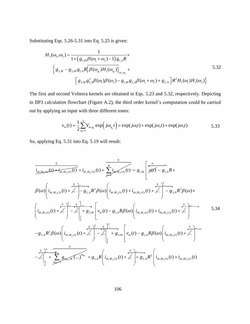
106
Substituting Eqs. 5.26- 5.31 into Eq. 5.25 is given:
1 11 2
2 1 2
1, 1 2 1,
2, 2, 1, 1,
2 2
2, 1, 1 2 1, 2, 1 2 2, 1 1 1 2
1( , )
1 ( ) 1
( ) ( )
( ) ( ) ( ) ( ) ( )
M A
M M A q q
M A M A A
Hg g R
g g g R H
g g g g g R H H
5.32
The first and second Volterra kernels are obtained in Eqs. 5.23 and 5.32, respectively. Depicting
in IIP3 calculation flowchart (Figure A.2), the third order kernel’s computation could be carried
out by applying an input with three different tones:
1 1
1
3
, 1 2 3
1
1( ) exp exp( ) exp( ) exp( )
2in in q q
q
v t V j t j t j t j t
5.33
So, applying Eq. 5.31 into Eq. 5.19 will result:
2 2, (1) , (2)( ) ( )ds M ds Mi t i t2 2
0
, (3) , ( )
4
( ) ( )N
ds M ds M n
n
i t i t
0
1, ( )Mg x t
2
0
1,
, (3)( ) ( ) ...
A
ds M
g R
i t
2 2
0
2
2, , (1) , (2)( ) ( ) ( ) ...A ds M ds Mg R i t i t
2
20
3
3,
, (1)
( )
( ) ...
A
ds M
g R
i t
30
...
2 2
0
2, 1, , (1) , (2)( ) ( ) ( ) ( ) ...M in A ds M ds Mg v t g R i t i t
2
0
2
2, , (1)( ) ( ) ...A ds Mg R i t
20
...
2
20
3, 1, , (1)( ) ( ) ( ) ...M in A ds Mg v t g R i t
0
...
30
,
3
...M
M
M
M
Nm
m M
m
g
2
0
1, , (3) ( ) ...A ds Mg R i t 2 2
0
2
2, , (1) , (2)( ) ( )A ds M ds Mg R i t i t
5.34

107
...2
20
3
3, , (1) ( ) ...A ds Mg R i t
30
,
3
...A
A
A
A
Nm
m A
m
g
0
Simplifying Eq. 4.18 5.34 yields:
2 2
2 2 2
2 2 2
33
, (3) 1, 1, 1, 3, , (1)
2 32 3
1, 2, , (1) , (2) 3, , (1)
22
2, 1, , (1) , (2) 2, , (1)
( ) 1 ( ) ( )
( ) ( ) ( ) ( ) ( )
( ) ( ) ( ) ( ) ( ) ( )
ds M M A A A ds M
M A ds M ds M A ds M
M in A ds M ds M A ds M
i t g g R g R g R i t
g g R i t i t g R i t
g v t g R i t i t g R i t
2 2 2
2
3 22
3, 1, , (1) 2, , (1) , (2)( ) ( ) ( ) ( ) ( )M in A ds M A ds M ds Mg v t g R i t g R i t i t
5.35
Expanding and extracting only the third order terms brings out:
2 2 2
2 2
2 2
2
1, 1, 1, , (3) 1, 2, , (1) , (2)
22 2 2
2, 1, , (2) 2, , (1) 1,
3
, (1) , (2) 1, 2,
1 ( ) ( ) 2 ( ) ( ) ( )
2 ( ) ( ) ( ) 2 ( ) ( ) ( ) 2
( ) ( ) ( ) ( ) 2
M A A ds M M A ds M ds M
M A in ds M A in ds M A
ds M ds M A A
g g R g R i t g g R i t i t
g g Rv t i t g R v t i t g R
i t i t g g R
2 2
2 2
2 2 2 2
2
, (1) , (1)
23 2 2 2 3
3, 1, , (1) 1, , (1) 1,
33 2 3
, (1) 2, , (1) , (2) 3, 1, , (1)
( ) ( ) ( ) ( )
( ) 3 ( ) ( ) ( ) 3 ( ) ( ) ( )
( ) ( ) 2 ( ) ( ) 1 ( )
ds M ds M
M in A in ds M A in ds M A
ds M A ds M ds M A M ds M
i t i t
g v t g Rv t i t g R v t i t g
R i t g R i t i t g R g i
3
( )t
5.36
Same as process was done over Eq. 4.19, the third-order terms in Eq. 5.36 should be translated to
first, second, and third order kernels as well as the extraction of their coefficients. However, the
number of terms influences us to analyses each term separately due to simplicity in tracing the
equations.
21 2 3
1, 1, 1, , (3), ,
3
1 ( ) ( )
1
2
M A A ds Mg g R g R i t
1 2 3, , ,in q in q in qV V V
1 2 3
1 2 3
1 2 3 1 2 3
3 3 3
1, 1, 1,
1 1 1
3
1, 1, 1 2 3 1, 3 1 2 3 1 2 3
1 ( )
( , , ) exp ( )
6 1 ( ) ( , , ) exp ( )
M A q q q A
q q q
q q q q q q
M A A
g g R g R
H j t
g g R g R H j t
5.37

108
In Eq. 5.36, for the rest of the terms that includes a pair of the first and second order terms, the
following frequencies’ distribution is required:
2
2 2
, (1) 1 2 3
2
, (2) , (1) 2 3 1 3 1 2
, ( )
, , , ,
ds M in
ds M ds M
i v t
i i
5.38
By the aid of Eq. 5.38, the rest of calculation would be as following:
2 21 2 3
2
1, 2, , (1) , (2), ,
2
1, 2,
2 ( ) ( ) ( )
12 ( )
2
M A ds M ds M
M A
g g R i t i t
g g R
1,in qV
1 1
1
3
1
1
2
( ) exp( )
1
2
q q
q
H j t
2 3, ,in q in qV V
2 3 2 3
2 3
1 2 31 2 3
3 3
2
1 1
2
1, 2, 1 2 3 1 1 2 2 3 1 2 2 1 3
1 3 2 1 2 1 2 3
2
1, 2, 1 2 3 1 2 1 2 3, ,
( , ) exp ( , )
4 ( ) ( ) ( , ) ( ) ( , )
( ) ( , ) exp ( )
4 ( ) ( ) ( , ) exp ( )
q q q q
q q
M A
M A q q q
H j t
g g R H H H H
H H j t
g g R H H j t
5.39
21 2 3
2, 1, , (2), ,
2, 1, 1 2 3 2 2 3 2 3
2 1 3 2 1 3 1 3
3 1 2 2 1 2 1 3
2, 1, 1 2 2
2 ( ) ( ) ( )
2 2exp( ) ( ) ( , ) exp ( )
2exp( ) ( ) ( , ) exp ( )
2exp( ) ( ) ( , ) exp ( )
4 ( ) (
M A in ds M
M A
M A
g g Rv t i t
g g R j t H j t
j t H j t
j t H j t
g g R H
1 2 1 2
1 2 3
1 2 1 3 2 1 3
2 3 2 2 3 1 2 3
2, 1, 2 1 2 3, ,
, ) ( ) ( , )
( ) ( , ) exp ( )
4 ( ) ( , ) exp ( )M A q q q q
H
H j t
g g R H j t
5.40
2
1 2 3
22
2, 2, , (1), ,
2
2, 2, 1 2 3 1 2 1 3 2 3
2 1 3 1 1 1 3 1 3
3 1 2 1 1 1 2 1 2
2 ( ) ( ) ( )
2 2exp( ) ( ) ( ) ( ) exp ( )
2exp( ) ( ) ( ) ( ) exp ( )
2exp( ) ( ) ( ) ( ) exp ( )
M A in ds M
M A
g g R v t i t
g g R j t H H j t
j t H H j t
j t H H j t
5.41

109
1 2 1 2
1 2 3
2
2, 2, 1 2 1 1 1 2 1 3 1 1 1 3
2 3 1 2 1 3 1 2 3
2
2, 2, 1 1 1 2 3, ,
4 ( ) ( ) ( ) ( ) ( ) ( )
( ) ( ) ( ) exp ( )
4 ( ) ( ) ( ) exp ( )
M A
M A q q q q
g g R H H H H
H H j t
g g R H H j t
2 21 2 3
2 2
2, 1, , (1) , (2), ,
2 2
2, 1, 1 1 1 1 2 3 2 2 3 2 3
2 1 2 2 1 3 2 1 3 1 3
3 1 3 3 1 2
2 ( ) ( ) ( ) ( )
2 2 ( ) ( ) exp( ) ( ) ( , ) exp ( )
2 ( ) ( ) exp( ) ( ) ( , ) exp ( )
2 ( ) ( ) exp( ) ( )
M A ds M ds M
M A
g g R i t i t
g g R H j t H j t
H j t H j t
H j t H
1 1 2 3 2 3
1 2 3
2 1 2 1 2
2 2
2, 1, 1 1 1 2 3 2 2 3
2 1 2 1 3 2 1 3
3 1 3 1 2 2 1 2 1 2 3
2 2
2, 1, 1 2 1, ,
( , ) exp ( )
4 ( ) ( ) ( ) ( , )
( ) ( ) ( ) ( , )
( ) ( ) ( , ) ( , ) exp ( )
4 ( ) ( ) ( ) ( , ) exp (
M A
M A q q q q q q
j t
g g R H H
H H
H H j t
g g R H H j
2 3)t
5.42
2 2
1 2 3
23
2, 1, 2, , (1) , (1), ,
3
2, 1, 2,
1 1 1 1 2 3 1 2 1 3 2 3
2 1 2 2 1 3 1 1 1 3 1 3
3 1 3
2 ( ) ( ) ( ) ( )
2
2 ( ) ( ) exp( ) ( ) ( ) ( ) exp ( )
2 ( ) ( ) exp( ) ( ) ( ) ( ) exp ( )
2 ( ) ( ) exp(
M A A ds M ds M
M A A
g g g R i t i t
g g g R
H j t H H j t
H j t H H j t
H j
1 2 31 2 3
3 1 2 1 1 1 2 1 2
3
2, 1, 2, 1 2 3 2 1 3 3 1 2
1 1 1 2 1 3 1 2 3
3
2, 1, 2,, ,
1 1 1 2 1 3 1 2 3
) ( ) ( ) ( ) exp ( )
4 ( ) ( ) ( ) ( ) ( ) ( )
( ) ( ) ( ) exp ( )
4 ( ) ( )
( ) ( ) ( ) exp ( )
M A A
M A A q q q
t H H j t
g g g R
H H H j t
g g g R
H H H j t
5.43
1 2 3
3
3, 3, ,
1( )
2M ing v t
1 2 3, , ,in q in q in qV V V
1 2 3
1 2 3
3 3 3
1 1 1
3, 1 2 3
exp ( )
6 exp ( )
q q q
q q q
M
j t
g j t
5.44

110
21 2 3
2
3, 1, , (1), ,
3, 1, 2
3 ( ) ( ) ( )
13
2
M A in ds M
M A
g g Rv t i t
g g R
1 2, ,in q in qV V
1 2
1 2
3 3
1 1
exp ( )
1
2
q q
q q
j t
3,in qV
3 3 3
3
3
1
1
3, 1, 1 2 3 1 3 3
1 3 2 1 2 2
2 3 1 1 1 1
3, 1, 1 1 1 2 1 2 3 1 3
( ) ( ) exp( )
3 2exp ( ) ( ) ( ) exp( )
2exp ( ) ( ) ( ) exp( )
2exp ( ) ( ) ( ) exp( )
6 ( ) ( ) ( ) ( ) ( ) ( ) e
q q q
q
M A
M A
H j t
g g R j t H j t
j t H j t
j t H j t
g g R H H H
1 1
1 2 3
1 2 3
3, 1, 1 1 2 3, ,
xp ( )
6 ( ) ( ) exp ( )M A q q
j t
g g R H j t
5.45
2
1 2 3
22 2
3, 1, , (1), ,
2 2
3, 1,
3 ( ) ( ) ( )
13
2
M A in ds M
M A
g g R v t i t
g g R
1,in qV
1
1
3
1
2
exp( )
1
2
q
q
j t
2 3, ,in q in qV V
2 2 3 3 2 3
2 3
3 3
1 1
1 1
2 2
3, 1, 1 2 1 2 3 1 3 2 3
2 1 1 1 3 1 3 1 3
3 1 1 1 2 1 2
( ) ( ) ( ) ( ) exp ( )
3 2exp( ) ( ) ( ) ( ) ( ) exp ( )
2exp( ) ( ) ( ) ( ) ( ) exp ( )
2exp( ) ( ) ( ) ( ) ( ) exp
q q q q q q
q q
M A
H H j t
g g R j t H H j t
j t H H j t
j t H H j
1 1 2 2
1 2 3
1 2
2 2
3, 1, 1 1 1 2 1 2 1 1 1 3 1 3
2 1 2 3 1 3 1 2 3
2 2
3, 1, 1 1 1 2 3, ,
( )
6 ( ) ( ) ( ) ( ) ( ) ( ) ( ) ( )
( ) ( ) ( ) ( ) exp ( )
6 ( ) ( ) ( ) ( ) exp ( )
M A
M A q q q q
t
g g R H H H H
H H j t
g g R H H j t
5.46

111
2
1 2 3
33 3
3, 1, , (1), ,
3 3
3, 1, 3
( ) ( )
1
2
M A ds M
M A
g g R i t
g g R
1 2 3, , ,in q in q in qV V V
1 1 2 2
1 2 3
3 3 1 2 3
3 3 3
1 1
1 1 1
1
3 3
3, 1, 1 2 3 1 1 1 2 1 3 1 2 3
( ) ( ) ( ) ( )
( ) ( ) exp ( )
6 ( ) ( ) ( ) ( ) ( ) ( ) exp ( )
q q q q
q q q
q q q q q
M A
H H
H j t
g g R H H H j t
5.47
2 21 2 3
2
2, , (1) , (2), ,
2
2,
2 ( ) ( )
12
2
A ds M ds M
A
g R i t i t
g R
1,in qV
1 1
1
3
1
1
2
( ) exp( )
1
2
q q
q
H j t
2 3, ,in q in qV V
2 3 2 3
2 3
1 2 31 2 3
3 3
2
1 1
2
2, 1 1 2 2 3 1 2 2 1 3
1 3 2 1 2 1 2 3
2
2, 1 2 1 2 3, ,
( , ) exp ( , )
4 ( ) ( , ) ( ) ( , )
( ) ( , ) exp ( )
4 ( ) ( , ) exp ( )
q q q q
q q
A
A q q q
H j t
g R H H H H
H H j t
g R H H j t
5.48
2
1 2 3
1 2 3
33
3, 1, , (1), ,
3
3, , , ,
1 ( ) ( )A M ds M
A in q in q in q
g R g i t
g R V V V
1 2 3
1 2 3
2 2 3 1 2 3
3 3 3
1,
1 1 1
1 1 1
3
3, 1, 1 2 3 1 1 1 2 1 3 1 2 3
1 ( )
( ) ( ) ( ) exp ( )
6 1 ( ) ( ) ( ) ( ) exp ( )
M q q q
q q q
q q q q q q
A M
g
H H H j t
g R g H H H j t
5.49
Substituting Eq. 5.37 and 5.39- 5.49 into Eq. 5.36 is given:

112
1 2 31 2 3
1 1 2 3 2 31 2 3
3 1 2 3
1, 1, 1 2 3
2 2 2
2, 1, 1 2 3 1 2 2, 1,, ,
1 2 3, 1, 1 2 3, ,
2, 1, 2,
1( , , )
6 1 ( ) 1
4 1 ( ) ( ) ( , ) 4
( ) ( ) ( ) ( , ) 6 1 ( )
4
A M
A M q q q M A
q q q q q q A M
M A A
Hg R g
g R g H H g g R
H H g g
g g g
1 2 31 2 3
1 2 1 21 2 3
1 1 1 2 1 21 2 3
3 3
3, 1, 1 2 3 1 1, ,
1 2 1 3 2, 1, 2 3, 1,, ,
2 2
1 2, 2, 3, 1,, ,
( ) ( ) 6 ( ) ( ) ( ) ( )
( ) ( ) 4 ( ) ( , ) 6 1
( ) ( ) 4 ( ) 6 ( ) ( )
q q q M A
M A q q q q M A
q q M A q q M A q q
g g R H
H H g g R H g g R
H R g g g g
1 2
1 2 31 1
, ,( ) ( )q qH H
5.50
So far, all the Volterra kernels required for IIP3 computation are collected. The reminded task is
to prepare and substitute them in A.20. Based on this explanation the 1( )H and 1( )H ,
2 ( , )H and 2( , )H , and 3( , , )H is calculated from Eq. 5.23, 5.32, and 5.50,
respectively, as follow:
1,
1
1, 1,
( )1 ( ) 1
M
M A
gH
g g R
5.51
1,
1
1, 1,
( )1 ( ) 1
M
M A
gH
g g R
5.52
2
1, 1,
2 2 2 2
2, 2, 1, 1 2, 1, 1, 2, 2, 1
1( , )
1 (2 ) 1
2 ( ) ( ) ( ) (2 ) ( )
A M
M M A M A M A A
Hg R g
g g g R H g g g g g R H
5.53

113
2
1, 1,
2, 2, 1, 1 1
2 2 2
2, 1, 1, 2, 2, 1 1
1( , )
1 (0) 1
( ) ( ) ( ) ( )
( ) (0) ( ) ( )
M A
M M A
M A M A A
Hg g R
g g g R H H
g g g g g R H H
5.54
3
1, 1,
2
2, 1, 1 2 1 2
2 2
2, 1, 1 2 1 2
3, 1, 2, 1, 2,
3
3, 1,
1( , , )
6 1 ( ) 1
4 1 ( ) 2 ( ) ( , ) ( ) ( , )
4 ( ) 2 (0) ( ) ( , ) (2 ) ( ) ( , )
6 1 ( ) 4 ( ) 2 (0) (2 )
6
A M
A M
M A
A M M A A
M A
Hg R g
g R g H H H H
g g R H H H H
g g g g g
g g
3 3 2
1 1 3, 1, 1 1
2 2
2, 1, 2 2 3, 1,
2
1 1 2, 2, 1 1 1
( ) ( ) ( ) 6 1 ( ) 2 ( ) ( )
4 2 (0) ( , ) (2 ) ( , ) 6 ( )
( ) 2 ( ) 4 (2 ) ( ) 2 (0) ( ) ( )
M A
M A M A
M A
R H H g g R H H
g g R H H g g
H H g g H H R H
5.55
Due to the fact that the feedback factor is almost equal to zero at low frequencies, ( (0) 0 ),
Eq. 5.54 and 5.55 would simplified as:
2
1,
2, 2, 1, 1 1
2 2 2
2, 1, 2, 1 1
1( , )
1
( ) ( ) ( ) ( )
( ) ( ) ( )
A
M M A
M A A
Hg R
g g g R H H
g g g R H H
5.56

114
3
1, 1,
2
2, 1, 1 2 1 2
1, 1 3, 2, 1, 2
2 3 3
3, 1, 2, 1, 2, 3, 1,
1( , , )
6 1 ( ) 1
4 1 ( ) 2 ( ) ( , ) ( ) ( , )
1 ( ) ( ) 6 4 (2 ) ( , )
6 1 ( ) 4 ( ) (2 ) 6 ( )
A M
A M
A M M A
A M M A A M A
Hg R g
g R g H H H H
g R H g g g R H
g g g g g g g
3 2
1 1 3, 1, 1
2 2 2
3, 1, 1 1 2, 2, 1 1
( ) ( ) 6 1 2 ( ) ( )
6 ( ) ( ) 2 ( ) 4 (2 ) ( ) ( )
M A
M A M A
R H H g g R H
g g H H g g H R H
5.57
Assuming R ≈ 1/g1,M , g2,A ≈ 0, and g1,A = α g1,M, where α<1, Eq. 5.51 and 5.57 would be:
1,
1
1, 1,
( )1 ( ) 1
M
M A
gH
g g R
5.58
3, 3, 3
2
3, 3, 2,,2
3,
3
( ) ( ) ( ),
( )( , )
M A
D
M A Mg g gH
A A A
A
5.59
where
1, 1,
2
22
3,
3 2 3 3
1, 1, 1,
( ) 1 ( )
( ) ( ) ( )
( ) 2 6 7
2
M M
M M
M
M
g g
g
A
g g
5.60
2 2
1, 1,
3,2
,
2
1
(2 )
(
( ) 2 (1
) 1 ( ) 1 ( ) ( ) (
)
1 2 2 1 2 2 )M M Mg
A
g g
5.61
1, 1,3, ( ) 3 1 1( ) (23 )1M MAA g g 5.62
1, 1,
3
13 ,, ( ) 3 1 1 1 1( ) ( ) 1 )1 (2D M M MA g g g 5.63
Consequently, by applying Eq. 5.58 and 5.59 in Eq. A.20 it can be concluded to:

115
1,
2
1, 3, 3, 2, ,2 ,,
43
3
( )
1 1 ( ) ( ) ( )( )
Num
D M D A D
M
M M A M
A
A
gIIP
g gAg g A
5.64
where
1, 1,
2 2 3 3
1, 1, 1,
22
,
3
( ) 1 ( )
( ) ( ) ( )
( ) 2 6 7
2
D M M M
M M M
g
g
A g
g g
5.65
2 2
1, 1, 1,
,2
2
(2 )
( )
( ) 2 (
1 ( ) 1 ( ) ( )
1 )
1 2 1 2 2 ( )2 M M M
DA
g g g
5.66
1 ,, , 1( )( () 3 1 3)1 21D A M MA g ag g 5.67
1,
3
1,( ) 1 (1 1 1) ( )M MNum g gA 5.68
As it is apparent from the above analytical derivations, this method takes into account a wider
range of nonlinear elements’ effects, as compared to the pervious works. In fact, considering the
more derivative orders of the auxiliary current allows for a comprehensive description of the
feedback impact, as well as providing a higher level of linearity.
5.3.3 Noise Cancelation
One of the interesting points regarding to the CC-LNA with NF-IMS method compare to IMS
method is its noise performance. As it is predictable, NF of a circuit would experience an
increase when an additional active device like a transistor is added to its structure. This scenario
will be applied to NF of the optimized CC-LNA when the IMS method and AuxM present to it.
However, the NF-IMS method restores some of these noise performance side effects. In other
words, the proposed method shows a degree of noise cancellation behavior, which promotes a
decrease in NF IMSNF respect to IMSNF . To have been better over-view on this improvement, the
mean square of noise at node Q due to the channel thermal noise sources of MainM and AuxM

116
provides an essential comparison means for us. Thus, applying Kirchhoff's current and voltage
low (KCL and KVL), the Qv for CC-LNA with IMS and NF-IMS will calculate as follows:
2 2 2 2 2
, , ,2
, 2 2 2 2
, ,2 ,
(1 )
(1 )( )
nd M m M S nd A
Q IMS
m M S m m A
i g L iv
g L g g
5.69
2 2 2 2 2
, , 1 ,2
, 22 2
,2 , ,2 , , 1 , ,2 2
(1 )
( ) ( )
nd M m M S nd A
Q NFIMS
m m A m m A m M S m M m S
i g L iv
g g g g g L g g L
5.70
Where ,nd Mi and ,nd Ai represent the channel thermal noise sources of main and auxiliary
transistors, respectively. Assuming 1S SL L , 2 1S SL L , and ,2 , m m Mg g where 1 .
Substituting them in Eq. 5.69 and 5.70 lead to:
2 2 2 2 2
, , ,2
, 2 2 2 2 2
, ,
(1 )
(1 )( )
nd M m M S nd A
Q IMS
m M S m M
i g L iv
g L g
5.71
2 2 2 2 2 2
, , ,2
, 2 2 2 2 2 2
, ,
(1 )
( ) ( )
nd M m M S nd A
Q NFIMS
m M S m M
i g L iv
g L g
5.72
A comparison between Eq. 5.71 and 5.72 shows a roughly 10% improvement in NF IMSNF . A
comprehensive explanation to this phenomenon is the noise source of the main transistor
presents two voltages with opposite phase at the drain and source of it. Later, the drain noise will
be sampled by the auxiliary pass and added to the source node. Because of the phase difference,
they would nullify each other. The same story could be applied to ,nd Ai while this time the main
transistor samples the drain of auxiliary one.

117
(a) (b)
(c) (d)
Figure 5.3: The S-parameters and NF result of CC-LNA with and without nonlinearity
enhancement.
21(
)S
dB
( )f GHz
CC LNA NF IMS CC LNA IMS CC LNA
()
NF
dB
( )f GHz
CC LNA NF IMS CC LNA IMS CC LNA
11(
)S
dB
( )f GHz
CC LNA NF IMS CC LNA IMS CC LNA
22(
)S
dB
( )f GHz
CC LNA NF IMS CC LNA IMS CC LNA

118
5.4 Simulation and Results
The NF-IMS method parameters’ specifications are discussed as follow; first, the
transistor, capacitors, and inductor size of the core LNA are optimized with respect to gain, NF,
input matching, and power consumption. Then, the size and number of fingers of the auxiliary
transistor is investigated to achieve a maximum IIP3 and minimum DC power.
To increase the practical reliability of this simulation, we employ the real element model
from TSMC 65nm CRN65GP rather than the ideal one. Besides, in order to simulate and
measure the IIP3, the two-tone test is conducted by applying harmonic balance analysis. To
indicate the robustness of proposed method, the selected tones are absolutely close to each other
with 1MHz frequency separation.
Figure 5.4: IIP3 result of CC-LNA with and without nonlinearity enhancement.
()
out
PdB
m
( )inP dBm
CC LNA NF IMS CC LNA IMS CC LNA
Third order
Fundamental

119
Figure 5.5: IIP3 as function of PMOS’s width for auxiliary biasing equals to 0V.
Figure 5.6: IIP3 as function of PMOS’s width for auxiliary biasing equals to 0V.
()
out
PdB
m
( )inP dBm
CC LNA NF IMS CC LNA IMS CC LNA
Third order
Fundamental
fK
( )f GHz
CC LNACC LNA NF IMS

120
As depicted in Figure 5.3 and Figure 5.4, the designed CC-LNA with real model
elements presents 22.4dB gain ( 21S ), 1.24dB NF, -12.38dB input impedance matching ( 11S ),
-7.44dBm IIP3, and 12.62mW power consumptions from a 1.2V power supply. Moreover, Fig. 7
represents that the minimum unconditional stability ( fK ) factor is 2.2 at 2.4GHz.
Based on the (24), the variable α plays a critical role in IIP3 calculation. Due to the fact
that CC-LNA parameters are constant and they would not be affected by linearization methods,
can be considered just as function of the width and gate biasing of the PMOS. It allows us to
assume the variation of IIP3 as a function of the auxiliary transistor’s width and biasing. The
demonstrated curve in Figure 5.5 reveals the relation between IIP3 and the PMOS’s width. In
addition, the variation of IIP3 and DC power as function of auxiliary transistor’s gate biasing are
shown in Figure 5.7.a and 5.7.b, respectively. As it is apparent, the optimum value for the IIP3 is
occurs for the PMOS with 140µm width and a gate bias of 0V. As depicted in Figure 5.7.c and
5.7.d, the relation between the linearity and the number of the fingers for the auxiliary transistor
is not as effective as width of the PMOS. In other words, the IIP3 and power consumption are
not sensitive to number of fingers.
Base on the above consideration and results of Figure 5.3 and Figure 5.4, the designed
LNA with NF-IMS method presents a maximum 21S of 16.67dB, minimum 11S of -11.78dB,
1.26dB minNF , and 2.08dBm IIP3, while dissipate 16.9mW power from a 1.2V power supply.
Consistently with our expectation, the negative feedback improves the unconditional stability
factor. The new ,f minK is 4.8 which are two times larger than the previous one (Fig. 7).
Based on the above results, it’s clear that the NF-IMS method had been strongly
improved the CC-LNA characteristics. However, to prove the effectiveness of the proposed
NF-IMS method, an investigation could be conducted between the IMS method’s results and the
above ones. To have a fairly comparison, the size and biasing of transistors, value of the passive
element, and power’s level of the input signal are identical for the both tests. As Figure 5.3 and
Figure 5.4 demonstrate, the designed CC-LNA with IMS methods shows the maximum forward

121
(a) (b)
(c) (d)
Figure 5.7: IIP3 and dissipation power as function of the auxiliary transistor; (a) and (b)
width and biasing, (c) and (d) number of fingers and biasing
3(
)II
PdB
m
, ( )b AV V(
)D
CP
mW
, ( )b AV V
50 m
112 m
130 m
300 m
237 m
175 m
143 m
3(
)II
PdB
m
, ( )b AV V
()
DC
Pm
W
, ( )b AV V
1
4
7
17
14
10
8
20

122
gain (21S ) of 15.83dB, -16.56dB as the minimum input return loss (
11S ), 1.51dB for the
minimum NF, and IIP3 of 0.54dBm, while consumes 16.88mW from 1.2V power supply.
A simple calculation reveals the 1.5dBm improvement in IIP3 of NF-IMS method
compares to the IMS one. In addition to nonlinearity, it’s also slightly enhancing the 21S and NF
while dissipating almost same power as IMS method uses.
5.5 Conclusion
A CMOS LNA designed based on NF-LMS methods has been presented. As a result of
the negative feedback, a highly linear amplifier is proposed with unconditional stability and low
power consumption. According to the analyses and simulations, the suggested design provides
more than 9dBm IIP3 improvement, while presenting as high gain as 16.67.6dB. The designed
LNA based on this method could be employed as best candidate for the WBAN and WPAN
gateway’s receiver due to its high linearity characteristics.

123
Chapter 6
Conclusion and Future work
6.1 Conclusion
In this thesis a new optimization technique have been presented for the CMOS inverter
LNA. The proposed technique provides the ability of optimizing two transistors simultaneously
and taking into account all effective noise sources of inverter topology. Appling this optimization
approach, a novel high gain, low power, CMOS low noise current reused LNA circuit has been
designed for the WBAN applications, which employs noise optimization technique to achieve
higher performance. The suggested solution applies noise equations to achieve low noise figure
and high gain simultaneously. The presented theoretical analyses and design methodologies are
aimed to cover the weakness of previous reported techniques. The theoretical procedure involved
fundamental concept and principals of noise parameters expressions and provided critical
assumptions to simplify the complicated relationships between noise parameters and circuit
elements. Considering the fact that there is no pure analytic approach for acceptable optimizing
of CMOS inverter several numerical investigation and simulations where utilized to obtained
optimum values.
The LNA’s circuit has been designed and simulated based on IBM o.13 µm and TSMC
65 nm. The circuit attained 28.5 dB gain, 2.4 dB noise figure, -18 dB impedance matching, and
power dissipating less than 1mW at 2.4 GHz frequency.
In addition, a novel linearization technique was introduced based on the Cascaded-LNA
(CC-LNA) structure. Utilizing this technique, we attained a highly linear device that provides a
1.5dB IIP3 improvement without affecting NF or gain. This architecture was aimed to be used in
gateway applications. The importance of the suggested method will be more clear by considering
the fact that no extra element was used in the structure.
6.2 Future work
There are several improvements can be applied to the techniques and designs that was
described. The optimization technique that was presented in chapter Chapter 3 is capable to

124
apply to the other frequency bands of NB-WBAN. It would be good practice to design the CICR
LNA for the lower frequency as well as UWB-WBAN frequencies.
The inductors used in the LNAs were modeled with the inductor model kits from the
either IBM 0.13 µm or TSMC 65 nm design kits. Although, these models were carried out at the
time of the design, the extended model form an electromagnetic (EM) simulator can improve the
accuracy of simulation.
Besides the above design enhancement, providing layout, chip fabrication, and test and
measurement are of other future works.

125
Appendix A
Volterra Series Tutorial
A.1. History
The low noise amplifiers should be analyzed as a weakly nonlinear time invariant
system with memory effects, in which the term “weakly nonlinear” denotes the condition of
small input excitation that can be modeled with polynomials. The memory effect is
originated from energy storage elements such as capacitors and inductors in which the output
is depended to both the current input and the previous one. At high frequencies, unlike the
low frequencies, there is not sufficient time for discharging the pervious input thoroughly.
Thus, memory effects must be taken into the account. Taylor series is not efficient in
predicting high-frequency-low-distortion terms due to the discrepancy of the analysis. The
power-series analysis is also improper for LNA analyzing since it can be applied only for the
systems with separated frequency-sensitive linear part from memory less nonlinear elements,
as shown in Figure A.1.a. As a result, the best method for analyzing such a system is the
Volterra series, which is valid for weakly nonlinear systems.
A.2. Volterra Series Analysis
In the theory of linear systems, it is postulated that the output ( )Y t can be written as:
(a)
(b)
Figure A.1: a) Typical nonlinear system with memory effects, b) Weakly nonlinear
system model for Volterra series analysis.
( )X t ( )Y t

126
( ) ( ) ( )Y t h X t d
A.1
where ( )h t denotes the impulse response to the Direct-delta function ( ( )t ) [93].
Figure A.1.b shows the model employed for Volterra-series approach, in which the circuit
could be a combination of linear and nonlinear elements and may have memory or feedback.
They also can be resistive or reactive. The excitation ( )X t is a series of a number of
individual sinusoidal components of non-commensurate frequencies. The voltage
corresponds to ( )X t can be written as:
1 1 1 1 1 1
1 1
1
*
, , ,
10
1 1( ) exp( ) exp( ) exp( )
2 2
Q Q
X q q X q q X q q
q q Qq
X t V j t V j t V j t
A.2
where 1 1
*
, ,X q X qV V , 1 1q q ,
1
*
,X qV is the complex conjugate of 1,X qV , and we assume that
there is no DC component in the excitation and the response. The only DC excitation
component in RF systems is the bias which can be implicitly comprised by assessing the na
coefficients at the bias point. However, the response of a nonlinear system to a sinusoidal
excitation includes DC term. In a weakly nonlinear circuit with small excitation, this DC
term is negligible. Thus, in LNA analysis the output DC component can only affects the bias
currents and voltages offset. It is worth mentioning that in the case of high offset bias, neither
power series nor volterra series is convenient. Considering the above assumption, the
excitation ( )X t , the incremental small signal voltage or current can be expressed as::
1 1
1
,
1( ) exp( )
2
Q
X q q
q Q
X t V j t
A.3
in which 1 0q . Norbert Wiener, who modified the Volterra series analysis to nonlinear
systems, proved that the weakly nonlinear circuit with small excitations response can be
presented as [73, 94]:

127
1 1 1 1 2 1 2 1 2 1 2( ) ( ) ( ) ( , ) ( ) ( ) ...Y t h X t d h X t X t d d
A.4
where 1 2( , ,..., )n nh is the nth-order kernel (or nonlinear impulse response) and the
nonlinear transfer function 1 2
( , ,..., )nn q q qH is its n-dimensional Fourier and transform. It
can be shown that this series is convergent and magnitude of each consecutive term is less
than the previous one. We can rewrite Eq. A.4in the compact form with limited series to N
terms (Nth-order) as:
1
( ) ( )N
n
n
Y t Y t
A.5
where
1 2 1 2 1 2( ) ... ( , ,..., ) ( ) ( )... ( ) ...n n n n nY t h X t X t X t d d d
A.6
By replacing Eq. A.3 into Eq. A.6 and applying the interchange methodology of the order of
integration and summation, the frequency-domain response will be obtained as:
1 2 1 2
1 2
1 2
, , ,
1 2 1 2 1 2
1( ) ... ... exp ( ... )
2
... ( , ,..., ) exp ( ... ) ...
n n
n
n
Q Q Q
n X q X q X q q q qnq Q q Q q Q
n n q q q n n
Y t V V V j t
h j d d d
A.7
where 0iq and the last term of Eq. A.7 is known as multidimensional Fourier transform:
1 2
1 2
1 2
1 2 1 2
( , ,..., ) ... ( , ,..., )
exp ( ... ) ...
n
n
n q q q n n
q q q n n
H h
j d d d
A.8
from which, the nonlinear impulse response can be attained through inverse-Fourier
transform:

128
1 2
1 2 1 2
1 2 2
1 2
1( , ,..., ) ... ( , ,..., )
(2 )
exp ( ... ) ...
n
n n
n n n q q q
q q q n q q q
h H
j d d d
A.9
As a result, the frequency domain response will be achieved as:
1 2 1 2
1 2
1 2
, , ,
1( ) ... ... ( , ,..., )
2
exp ( ... )
n n
n
n
Q Q Q
n X q X q X q n q q qnq Q q Q q Q
q q q
Y t V V V H
j t
A.10
that summation of ( )nY t over 1,2,...,n N results in ( )Y t . in other words, by summing the
individual nth-order responses, the final response will be attained. The advantage of Volterra
series approach is that we can separate the mixing products of the same order. Furthermore,
the nonlinear transfer function 1 2
( , ,..., )nn q q qH and the nth-order nonlinear impulse
response 1 2( , ,..., )n nh must be symmetrical in and , respectively. This statement will
be clear by considering the fact that the excitation ( )X t does not have any order associated
with different tones. As a result, permuting frequencies in ( )nY t should not change the
response.
A.3. Nonlinear transfer function
Harmonic input or probing method is the technique to find the nonlinear transfer
function. Assuming the excitation to be the simplest form of
1 2( ) exp( ) exp( ) ... exp( )nX t j t j t j t A.11
The nth-order part of a nonlinear circuit response can be determined, according to A.10, as:
1 2 1 2( ) ( , ,..., )exp ( ... )n n n n nY t t H j t A.12
where nt represents the number of specific term which is generated by the given multinomial
coefficients of input excitations.

129
,
1 1
!
!... ! !... !n k
Q Q
nt
m m m m
A.13
where n is the maximum possible number of all excitations for the particular nth-order term
and the im is number of repetition for an individual excitation ( i ). As a result, by replacing
A.12 in the circuit equation and retaining the nth-order term, the nonlinear transfer function
1 2( , ,..., )
nn q q qH will be found. Since the nth-order nonlinear transfer function is
depended on the transfer functions of the orders smaller than n, first we must employ
1( ) exp( )X t j t to calculate 1 1( )H , and then 2 1 2( , )H can be calculated by considering
1 2( ) exp( ) exp( )X t j t j t and using 1 1( )H and 1 2( )H . This procedure should be
followed to obtain all orders. Then, by calculating 1 2( , ,..., )n nH and applying A.10 and
A.5 the desired frequency components level in the whole response can be determined.
A.4. Single tone formulation for IIP3
A single-tone expression for the third order intercept point (IP3) can be computed
based on volterra kernels. The third order nonlinearity of the circuit with input tones of 1
and 2 is measured by IP3. As the input increases, these fundamental tones linearly increase
with a slope of 1in dB scale, however, the third order intermodulation (IM3) products
( 1 22 , 2 12 ) grow linearly with a slop of 3. The intersection point of these line
defined IP3. In other words, the input referred IP3 (IIP3) that is modulated by the system’s
gain is defined as output referred IP3 (OIP3), and can be expressed as [36]:
1 3
13
2i O OIIP P P P A.14
where, iP , 1OP , and 3OP are the input power, output power of the fundamental frequencies,
and output power of the IM3 frequencies, respectively. There are two methods for obtaining
IP3. One approach is a simulation based method and the other is analytical calculation of IP3
using Volterra kernels as follow [73]:

130
1 1
1 1 1 2
4 ( )3
3 ( , , )
HIIP
H
A.15
1 2
1 2 2 1
4 ( )3
3 ( , , )
HIIP
H
A.16
As the two fundamental tones of 1 and 2 are close to each other, we can write:
1 1 1 2( ) ( )H H A.17
1 1 1 2 1 2 2 1( , , ) ( , , )H H A.18
Thus, Eq. A.15 and A.16 can be used interchangeably. Once the Volterra kernels are
obtained analytically for a frequency, IP3 can be calculated based on only a single tone ( 1 ),
since 1 2 . Hence, we can have [95]:
1 1 1 2 1 2 2 1( , , ) ( , , )H H A.19
1 1
1 1 1 1
4 ( )3
3 ( , , )
HIIP
H
A.20
which in dB scale will be as [62]:
1 1
10
1 1 1 1
4 ( )3 20log 10
3 ( , , )dBm
HIIP dB
H
A.21
Although, IIP3 can be determined the capacitor and inductor memory and frequency effects,
it does not take into account the effects of the elements that are not modeled in the
transistor’s equivalent circuit, such as body effect, parasitic capacitances, gsC bias-
dependency, gate/source resistance, and channel length modulation. The following flow chart
summarized the Volterra kernel’s derivation process to be used in IIP3 calculation.

131
Figure A.2:IIP3 calculation flowchart of a nonlinear system.

132
Bibliography
[1] B. Razavi, RF Microelectronics, 2nd ed.: Prentice Hall, 2011.
[2] H. A. Haus, W. R. Atkinson, G. M. Branch, W. B. Davenport, W. H. Fonger, W. A. Harris, et al.,
"Representation of Noise in Linear Twoports," Proceedings of the IRE, vol. 48, pp. 69-74, 1960.
[3] S. P. Voinigescu, M. C. Maliepaard, J. L. Showell, G. E. Babcock, D. Marchesan, M. Schroter, et
al., "A scalable high-frequency noise model for bipolar transistors with application to optimal
transistor sizing for low-noise amplifier design," IEEE Journal of Solid-State Circuits,, vol. 32,
pp. 1430-1439, 1997.
[4] D. K. Shaeffer and T. H. Lee, "A 1.5-V, 1.5-GHz CMOS low noise amplifier," IEEE Journal of
Solid-State Circuits, vol. 32, pp. 745-759, 1997.
[5] P. Andreani and H. Sjoland, "Noise optimization of an inductively degenerated CMOS low noise
amplifier," IEEE Transactions on Circuits and Systems II: Analog and Digital Signal Processing,
vol. 48, pp. 835-841, 2001.
[6] D. Zhiming and A. M. Niknejad, "On the Noise Optimization of CMOS Common-Source Low-
Noise Amplifiers," IEEE Transactions on Circuits and Systems I: Regular Papers, vol. 58, pp.
654-667, 2011.
[7] S. Ullah, H. Higgins, B. Braem, B. Latre, C. Blondia, I. Moerman, et al., "A Comprehensive
Survey of Wireless Body Area Networks," Journal of Medical Systems, vol. 36, pp. 1065-1094,
2012/06/01 2012.
[8] B. Regal, Radio : the life story of a technology. Westport, Conn.: Greenwood Press, 2005.
[9] O. J. LODGE, US609154, Aug 16, 1898.
[10] G. MARCONI, US627650, Jun 27, 1899.
[11] E. H. Armstrong and R. C. o. America, The Legacies of Edwin Howard Armstrong: The
Regenerative Circuit, the Superheterodyne Circuit, the Superregenerative Circuit, Frequency
Modulation: Radio Club of America, 1990.
[12] K. B. Schad, H. Schumacher, and A. Schuppen, "Low-power active mixer for Ku-band
application using SiGe HBT MMIC technology," in Microwave Symposium Digest. 2000 IEEE
MTT-S International, 2000, pp. 397-400 vol.1.
[13] N. M. Madani, J. Hadi, and S. M. Fakhraie, "Design and implementation of a fully digital 4FSK
demodulator," in Circuit Theory and Design, 2005. Proceedings of the 2005 European
Conference on, 2005, pp. III/277-III/280 vol. 3.
[14] B. P. Lathi and Z. Ding, Modern digital and analog communication systems. New York: Oxford
University Press, 2010.
[15] L. W. Couch, Digital and Analog Communication Systems, 8th ed.: Pearson Education, 2013.
[16] R. V. L. Hartley, "Modulation System," U. S. Patent 1 666 206, Apr 17, 1928.
[17] D. K. Weaver, "A Third Method of Generation and Detection of Single-Sideband Signals,"
Proceedings of the IRE, vol. 44, pp. 1703-1705, 1956.
[18] T. Okanobu, H. Tomiyama, and H. Arimoto, "Advanced low voltage single chip radio IC,"
Consumer Electronics, IEEE Transactions on, vol. 38, pp. 465-475, 1992.
[19] B. Razavi, "Design of Millimeter-Wave CMOS Radios: A Tutorial," Circuits and Systems I:
Regular Papers, IEEE Transactions on, vol. 56, pp. 4-16, 2009.
[20] A. Mashhour, W. Domino, and N. Beamish, "On the direct conversion receiver - A tutorial,"
Microwave Journal, vol. 44, pp. 114-128, 2001.

133
[21] J. Vankka and K. A. Halonen, Direct digital synthesizers: theory, design and applications:
Springer, 2001.
[22] V. Giannini, J. Craninckx, and A. Baschirotto, Baseband analog circuits for software defined
radio: Springer, 2008.
[23] Z. Yuanjin, Y. Jiangnan, and X. Yong Ping, "A CMOS VGA With DC Offset Cancellation for
Direct-Conversion Receivers," Circuits and Systems I: Regular Papers, IEEE Transactions on,
vol. 56, pp. 103-113, 2009.
[24] M. Inamori, A. Bostamam, Y. Sanada, and H. Minami, "IQ imbalance compensation scheme in
the presence of frequency offset and dynamic DC offset for a direct conversion receiver,"
Wireless Communications, IEEE Transactions on, vol. 8, pp. 2214-2220, 2009.
[25] I. Kwon, "Low-power design of CMOS baseband analog chain for direct conversion receiver,"
International Journal of Circuit Theory and Applications, vol. 38, pp. 111-122, 2010.
[26] A. Mirzaei, H. Darabi, J. C. Leete, C. Xinyu, K. Juan, and A. Yazdi, "Analysis and Optimization
of Current-Driven Passive Mixers in Narrowband Direct-Conversion Receivers," Solid-State
Circuits, IEEE Journal of, vol. 44, pp. 2678-2688, 2009.
[27] S. Jin-Siang, M. Chin-Chun, T. Ya-Hui, and L. Hua-Yu, "Large Improvement in Image Rejection
of Double-Quadrature Dual-Conversion Low-IF Architectures," Microwave Theory and
Techniques, IEEE Transactions on, vol. 58, pp. 1703-1712, 2010.
[28] N. Trung-Kien, O. Nam-Jin, L. Viet-Hoang, and L. Sang-Gug, "A low-power CMOS direct
conversion receiver with 3-dB NF and 30-kHz flicker-noise corner for 915-MHz band IEEE
802.15.4 ZigBee standard," Microwave Theory and Techniques, IEEE Transactions on, vol. 54,
pp. 735-741, 2006.
[29] M. Camus, B. Butaye, L. Garcia, M. Sie, B. Pellat, and T. Parra, "A 5.4mW 0.07mm2 2.4GHz
Front-End Receiver in 90nm CMOS for IEEE 802.15.4 WPAN," in Solid-State Circuits
Conference, 2008. ISSCC 2008. Digest of Technical Papers. IEEE International, 2008, pp. 368-
620.
[30] C. Namjun, L. Jeabin, Y. Long, B. Joonsung, K. Sunyoung, and Y. Hoi-Jun, "A 60kb/s-to-
10Mb/s 0.37nJ/b Adaptive-Frequency-Hopping Transceiver for Body-Area Network," in Solid-
State Circuits Conference, 2008. ISSCC 2008. Digest of Technical Papers. IEEE International,
2008, pp. 132-602.
[31] K. Kyung-Sup, S. Ullah, and N. Ullah, "An overview of IEEE 802.15.6 standard," in Applied
Sciences in Biomedical and Communication Technologies (ISABEL), 2010 3rd International
Symposium on, 2010, pp. 1-6.
[32] IEEE 802.15 WPAN™ Task Group 6 (TG6) Body Area Networks. Available:
http://www.ieee802.org/15/pub/TG6.html
[33] Beno, #238, t. Latr, #233, B. Braem, I. Moerman, et al., "A survey on wireless body area
networks," Wirel. Netw., vol. 17, pp. 1-18, 2011.
[34] M. Chen, S. Gonzalez, A. Vasilakos, H. Cao, and V. M. Leung, "Body Area Networks: A
Survey," Mobile Networks and Applications, vol. 16, pp. 171-193, 2011/04/01 2011.
[35] L. Miaoxin and Z. Mingjie, "An overview of Physical layers on wireless body area network," in
Anti-Counterfeiting, Security and Identification (ASID), 2012 International Conference on, 2012,
pp. 1-5.
[36] J. Rogers and C. Plett, Radio Frequency Integrated Circuit Design, 2nd ed. Boston: Artech
House, 2010.
[37] B. Razavi, "Cognitive Radio Design Challenges and Techniques," Solid-State Circuits, IEEE
Journal of, vol. 45, pp. 1542-1553, 2010.

134
[38] A. J. Scholten, L. F. Tiemeijer, R. van Langevelde, R. J. Havens, A. T. A. Zegers-van
Duijnhoven, and V. C. Venezia, "Noise modeling for RF CMOS circuit simulation," Electron
Devices, IEEE Transactions on, vol. 50, pp. 618-632, 2003.
[39] J. J. Ou, J. Xiaodong, H. Chenming, and P. R. Gray, "Submicron CMOS thermal noise modeling
from an RF perspective," in VLSI Technology, 1999. Digest of Technical Papers. 1999
Symposium on, 1999, pp. 151-152.
[40] A. J. Scholten, H. J. Tromp, L. F. Tiemeijer, R. van Langevelde, R. J. Havens, P. W. H. de
Vreede, et al., "Accurate thermal noise model for deep-submicron CMOS," in Electron Devices
Meeting, 1999. IEDM '99. Technical Digest. International, 1999, pp. 155-158.
[41] T. H. Lee, The design of CMOS radio-frequency integrated circuits, 2nd ed. Cambridge, :
Cambridge University Press, 2004.
[42] R. P. Jindal, "Compact Noise Models for MOSFETs," Electron Devices, IEEE Transactions on,
vol. 53, pp. 2051-2061, 2006.
[43] G. D. J. Smit, A. J. Scholten, R. M. T. Pijper, R. van Langevelde, L. F. Tiemeijer, and D. B. M.
Klaassen, "Experimental Demonstration and Modeling of Excess RF Noise in Sub-100-nm
CMOS Technologies," Electron Device Letters, IEEE, vol. 31, pp. 884-886, 2010.
[44] C. C. Enz and E. A. Vittoz, Charge-based MOS transistor modeling : the EKV model for low-
power and RF IC design. Chichester: Wiley, 2006.
[45] A. Van Der Ziel, Noise in Solid State Devices and Circuits: Wiley, 1986.
[46] Y. Tsividis and C. McAndrew, Operation and modeling of the MOS transistor, 3rd ed. New
York: Oxford University Press, 2011.
[47] G. D. Vendelin, A. M. Pavio, and U. L. Rohde, Microwave Circuit Design Using Linear and
Nonlinear Techniques. Hoboken: John Wiley & Sons, 2005.
[48] S. C. Cripps, RF power amplifiers for wireless communications, 2nd ed. Boston: Artech House,
2006.
[49] N. Trung-Kien, K. Chung-Hwan, I. Gook-Ju, Y. Moon-Su, and L. Sang-Gug, "CMOS low-noise
amplifier design optimization techniques," IEEE Transactions on Microwave Theory and
Techniques, vol. 52, pp. 1433-1442, 2004.
[50] M. Yargholi and A. P. Tarighat, "Resistive feedback LNA with dual band notch filter for
suppressing WLAN signals in UWB receivers," in Communications (NCC), 2012 National
Conference on, 2012, pp. 1-4.
[51] L. Hiu Fai and H. C. Luong, "A 1.2-6.6GHz LNA using transformer feedback for wideband input
matching and noise cancellation in 0.13um CMOS," in Radio Frequency Integrated Circuits
Symposium (RFIC), 2012 IEEE, 2012, pp. 17-20.
[52] C. Ding, W. Zhang, D. Jin, H. Xie, Y. Zhao, Q. Fu, et al., "An inductorless high linear UWB
Cascode LNA with tunable active resistance feedback and post-linearization technique,"
Microelectronics Journal.
[53] H. Kuang-Chi, L. Ming-Tsung, L. Chen-Ming, and T. Jenn-Hwan, "Parallel-RC Feedback Low-
Noise Amplifier for UWB Applications," Circuits and Systems II: Express Briefs, IEEE
Transactions on, vol. 57, pp. 582-586, 2010.
[54] N. J. Oh, "Corrections to "CMOS Low-Noise Amplifier Design Optimization Techniques" [May
04 1433-1442]," Microwave Theory and Techniques, IEEE Transactions on, vol. 55, pp. 1255-
1255, 2007.
[55] N. Trung-Kien, K. Chung-Hwam, I. Gook-Ju, Y. Moon-Su, and L. Sang-Gug, "[Authors' reply to
comments on "CMOS low-noise amplifier design optimization techniques"]," Microwave Theory
and Techniques, IEEE Transactions on, vol. 54, pp. 3155-3156, 2006.

135
[56] F. Bruccoleri, E. A. M. Klumperink, and B. Nauta, Wideband low noise amplifiers exploiting
thermal noise cancellation. Dordrecht [u.a.]: Springer, 2005.
[57] Y. Yueh-Hua, Y. Yong-Sian, and Y. J. E. Chen, "A Compact Wideband CMOS Low Noise
Amplifier With Gain Flatness Enhancement," Solid-State Circuits, IEEE Journal of, vol. 45, pp.
502-509, 2010.
[58] F. Bruccoleri, E. A. M. Klumperink, and B. Nauta, "Wide-band CMOS low-noise amplifier
exploiting thermal noise canceling," Solid-State Circuits, IEEE Journal of, vol. 39, pp. 275-282,
2004.
[59] T. B. Merkin, L. Ju-Ching, J. Sungyong, L. Mingyu, J. Gao, and L. Sung Chul, "A 100-960MHz
CMOS Ultra-wideband Low noise Amplifier," in Circuits and Systems, 2008. MWSCAS 2008.
51st Midwest Symposium on, 2008, pp. 141-144.
[60] T. Thu Nga Tran, B. Chirn Chye, D. Manh Anh, and Y. Kiat Seng, "Reciprocal noise canceling
low power UWB LNA," in SoC Design Conference (ISOCC), 2009 International, 2009, pp. 13-
16.
[61] W. Keping, Y. Kiat Seng, M. Kaixue, and W. Zhigong, "An inductorless and capacitorless LNA
with noise and distortion cancelation," in Computer Research and Development (ICCRD), 2011
3rd International Conference on, 2011, pp. 270-274.
[62] S. C. Blaakmeer, E. A. M. Klumperink, D. M. W. Leenaerts, and B. Nauta, "Wideband Balun-
LNA With Simultaneous Output Balancing, Noise-Canceling and Distortion-Canceling," Solid-
State Circuits, IEEE Journal of, vol. 43, pp. 1341-1350, 2008.
[63] W. Hongrui, Z. Li, and Y. Zhiping, "A Wideband Inductorless LNA With Local Feedback and
Noise Cancelling for Low-Power Low-Voltage Applications," Circuits and Systems I: Regular
Papers, IEEE Transactions on, vol. 57, pp. 1993-2005, 2010.
[64] J. Yoon, H. Seo, I. Choi, and B. Kim, "Wideband LNA Using a Negative gm Cell for
Improvement of Linearity and Noise Figure," Journal of Electromagnetic Waves and
Applications, vol. 24, pp. 619-630, 2010/01/01 2010.
[65] W. Sanghyun, K. Woonyun, L. Chang-Ho, L. Kyutae, and J. Laskar, "A 3.6mW differential
common-gate CMOS LNA with positive-negative feedback," in Solid-State Circuits Conference -
Digest of Technical Papers, 2009. ISSCC 2009. IEEE International, 2009, pp. 218-219,219a.
[66] D. Ponton, P. Palestri, D. Esseni, L. Selmi, M. Tiebout, B. Parvais, et al., "Design of Ultra-
Wideband Low-Noise Amplifiers in 45-nm CMOS Technology: Comparison Between Planar
Bulk and SOI FinFET Devices," Circuits and Systems I: Regular Papers, IEEE Transactions on,
vol. 56, pp. 920-932, 2009.
[67] F. Xiaohua, Z. Heng, and E. Sanchez-Sinencio, "A Noise Reduction and Linearity Improvement
Technique for a Differential Cascode LNA," Solid-State Circuits, IEEE Journal of, vol. 43, pp.
588-599, 2008.
[68] T. Kihara, T. Matsuoka, and K. Taniguchi, "A transformer noise-canceling ultra-wideband
CMOS low-noise amplifier," IEICE Transactions on Electronics, vol. E93-C, pp. 187-199, 2010.
[69] T. Kihara, H. J. Park, I. Takobe, F. Yamashita, T. Matsuoka, and K. Taniguchi, "A 0.5 V Area-
Efficient Transformer Folded-Cascode CMOS Low-Noise Amplifier," Ieice Transactions on
Electronics, vol. E92C, pp. 564-575, Apr 2009.
[70] M. S. Mehrjoo and M. Yavari, "A low power UWB very low noise amplifier using an improved
noise reduction technique," in Circuits and Systems (ISCAS), 2011 IEEE International
Symposium on, 2011, pp. 277-280.
[71] Y. Rong-Fu, H. Tzyy-Sheng, and W. Jian-Ming, "Wideband common-gate low-noise amplifier
with dual-feedback for simultaneous input and noise matching," in Radio Frequency Integrated
Circuits Symposium (RFIC), 2011 IEEE, 2011, pp. 1-4.

136
[72] T. Kihara, T. Matsuoka, and K. Taniguchi, "A 1.0 V, 2.5 mW, transformer noise-canceling UWB
CMOS LNA," in Radio Frequency Integrated Circuits Symposium, 2008. RFIC 2008. IEEE,
2008, pp. 493-496.
[73] S. A. Maas, Nonlinear microwave and RF circuits, 2nd ed. Boston, Mass. [u.a.]: Artech House,
2003.
[74] B. Leung, VLSI for wireless communication, 2nd ed. New York; London: Springer, 2011.
[75] P. Wambacq and W. M. C. Sansen, Distortion analysis of analog integrated circuits. Boston:
Kluwer, 1998.
[76] M. C. Schneider and C. Galup-Montoro, CMOS Analog Design Using All-Region MOSFET
Modeling: Cambridge University Press, 2010.
[77] Z. Heng and E. Sanchez-Sinencio, "Linearization Techniques for CMOS Low Noise Amplifiers:
A Tutorial," Circuits and Systems I: Regular Papers, IEEE Transactions on, vol. 58, pp. 22-36,
2011.
[78] S. Narayanan, "Application of Volterra series to intermodulation distortion analysis of transistor
feedback amplifiers," Circuit Theory, IEEE Transactions on, vol. 17, pp. 518-527, 1970.
[79] R. Gharpurey, "Linearity Enhancement Techniques in Radio Receiver Front-Ends," Circuits and
Systems I: Regular Papers, IEEE Transactions on, vol. 59, pp. 1667-1679, 2012.
[80] J. Jiming and D. M. Holburn, "Design and analysis of a low-power highly linear mixer," in
Circuit Theory and Design, 2009. ECCTD 2009. European Conference on, 2009, pp. 675-678.
[81] Z. ZhiChao, M. R. Khan, C. Li, and D. Anh, "A broadband high linear LNA for GSM/LTE
wireless communications," in Electrical & Computer Engineering (CCECE), 2012 25th IEEE
Canadian Conference on, 2012, pp. 1-4.
[82] H. M. Geddada, J. W. Park, and J. Silva-Martinez, "Robust derivative superposition method for
linearising broadband LNAs," Electronics Letters, vol. 45, pp. 435-436, 2009.
[83] B. Toole, C. Plett, and M. Cloutier, "RF circuit implications of moderate inversion enhanced
linear region in MOSFETs," IEEE Transactions on Circuits and Systems I: Regular Papers,, vol.
51, pp. 319-328, 2004.
[84] V. Aparin, G. Brown, and L. E. Larson, "Linearization of CMOS LNA's via optimum gate
biasing," in Circuits and Systems, 2004. ISCAS '04. Proceedings of the 2004 International
Symposium on, 2004, pp. IV-748-51 Vol.4.
[85] D. Yongwang and R. Harjani, "A +18 dBm IIP3 LNA in 0.35 μm CMOS," in Solid-State
Circuits Conference, 2001. Digest of Technical Papers. ISSCC. 2001 IEEE International, 2001,
pp. 162-163, 443.
[86] T. W. Kim, "A Common-Gate Amplifier With Transconductance Nonlinearity Cancellation and
Its High-Frequency Analysis Using the Volterra Series," Microwave Theory and Techniques,
IEEE Transactions on, vol. 57, pp. 1461-1469, 2009.
[87] K. Tae Wook, K. Bonkee, and L. Kwyro, "Highly linear receiver front-end adopting MOSFET
transconductance linearization by multiple gated transistors," Solid-State Circuits, IEEE Journal
of, vol. 39, pp. 223-229, 2004.
[88] V. Aparin, "Linearization of CDMA receiver front-ends," Ph.D. 3167860, University of
California, San Diego, United States -- California, 2005.
[89] V. Aparin and L. E. Larson, "Modified derivative superposition method for linearizing FET low-
noise amplifiers," Microwave Theory and Techniques, IEEE Transactions on, vol. 53, pp. 571-
581, 2005.
[90] S. Ganesan, E. Sanchez-Sinencio, and J. Silva-Martinez, "A Highly Linear Low-Noise
Amplifier," Microwave Theory and Techniques, IEEE Transactions on, vol. 54, pp. 4079-4085,
2006.

137
[91] A. Liscidini, M. Brandolini, D. Sanzogni, and R. Castello, "A 0.13 µm CMOS front-end, for
DCS1800/UMTS/802.11b-g with multiband positive feedback low-noise amplifier," Solid-State
Circuits, IEEE Journal of, vol. 41, pp. 981-989, 2006.
[92] K. Tae-Sung and K. Byung-Sung, "Post-linearization of cascode CMOS low noise amplifier
using folded PMOS IMD sinker," Microwave and Wireless Components Letters, IEEE, vol. 16,
pp. 182-184, 2006.
[93] G. B. Arfken, H.-J. Weber, F. E. Harris, and ScienceDirect, "Mathematical methods for
physicists," vol. 7th, ed. Oxford: Academic, 2012.
[94] S. Ikehara and M. I. o. T. R. L. o. Electronics, A Method of Wiener in a Nonlinear Circuit:
Research Laboratory of Electronics, Massachusetts Institute of Technology, 1951.
[95] D. Tannir and R. Khazaka, "Computation of Intermodulation Distortion in RF Circuits Using
Single-Tone Moments Analysis," Computer-Aided Design of Integrated Circuits and Systems,
IEEE Transactions on, vol. 29, pp. 1121-1125, 2010.


![[Book] CMOS Current Amplifiers](https://img.dokumen.tips/doc/110x75/54e62e884a7959e23f8b47cb/book-cmos-current-amplifiers.jpg)