Embed Size (px)
Citation preview

CMOS COMPARATORS

COMPARATOR DESIGN CONSIDERATIONS
Comparator =
Preamp (optional in some cases)
+ Reference Subtraction (optional for single-bit case)
+ Regenerative Latch
Design Considerations
Accuracy (dynamic and static offset, noise, resolution)
Settling time (tracking BW, regeneration speed)
Sensitivity/resolution (gain)
Metastability (ability to make correct decisions)
Overdrive recovery (memory)
Power consumption
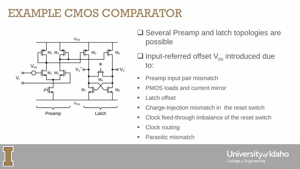
EXAMPLE CMOS COMPARATOR
Several Preamp and latch topologies are
possible
Input-referred offset Vos introduced due
to:
Preamp input pair mismatch
PMOS loads and current mirror
Latch offset
Charge-Injection mismatch in the reset switch
Clock feed-through imbalance of the reset switch
Clock routing
Parasitic mismatch
M1 M2
Vi
Vos
M3 M4
VDD
M5 M6
M8M7
M9
VSS
Φ
Vo+
Vo-
Preamp Latch

LATCH REGENERATION
Exponential regeneration due to positive feedback of cross-coupled pair M7 and M8
VDD
VSS
Vo
ΦPA tracking
Latch reseting
Latch
regenrating
Vo+
Vo-
VDD
M5 M6
M8M7
M9
VSS
ΦVo
+Vo
-
CL CL

REGENERATION SPEED – LINEAR MODEL
M8M7
CL CL
Vo+
Vo-
Vo-
Vo+
CL gmVo-
-1
out o m LV t V exp t g / C
pole RHP single ,/Cgs01/sCgsΔ LmpLm
0V
V
/sCg1
11
/sCVgV
VV
o
o
LmLomo
oo

REG. SPEED – LINEAR MODEL
(0)
oL
m o
V tCt ln
g V
M8M7
CL CL
Vo+
Vo-
Vo = 1VVo(t=0)
t
Vo Vo(t=0) t/(CL/gm)
1V 100mV 2.3
1V 10mV 4.6
1V 1mV 6.9
1V 100μV 9.2

REG. SPEED – LINEAR MODEL
Reg. Speed – Linear Model
amplifier. be to g
1
2
R,
Rg2
RgA
m7
9
9m7
9m5V2
M5 M6
M8M7
M9
Φ=1Vo
+Vo
-
Vm+
Vm-
M1 M2
Vi
M3 M4
Vm+
Vm-
Vo+
Vo-
R9
2
R9
2
-1
gm7
-1
gm7
gm5Vm+
gm5Vm-
X
m3
m1V1
g
gA
V2V1iVio AA0VA0V0V
LmV2V1io /CgtexpAA0VtV
x

COMPARATOR METASTABILITYReg. Speed – Linear Model
LmV2V1io /CgtexpAA0VtV
Curve AV1AV2 Vi(t=0)
10 10 mV
10 1 mV
10 100 μV
10 10 μV
Vo+
Φ
Vo-
1 2 3 4
T/2
Settling time is dependent upon initial signal and regenerative gain
When input is sufficiently close to the comparator threshold
Comparator fails to produce valid logic outputs within T/2
Sets the comparator resolution (Δ)

COMPARATOR METASTABILITYReg. Speed – Linear Model
Cascade pre-amp stages for larger gain
Pipelined multi-stage latches (with increased latency)
• pre-amp can be pipelined too
LSB1
ΔBER
LmV2V1io /CgtexpAA0VtV
Vi
DoΔ
j
Vos
j+1Assuming that the input is uniformly distributed over VFS, then
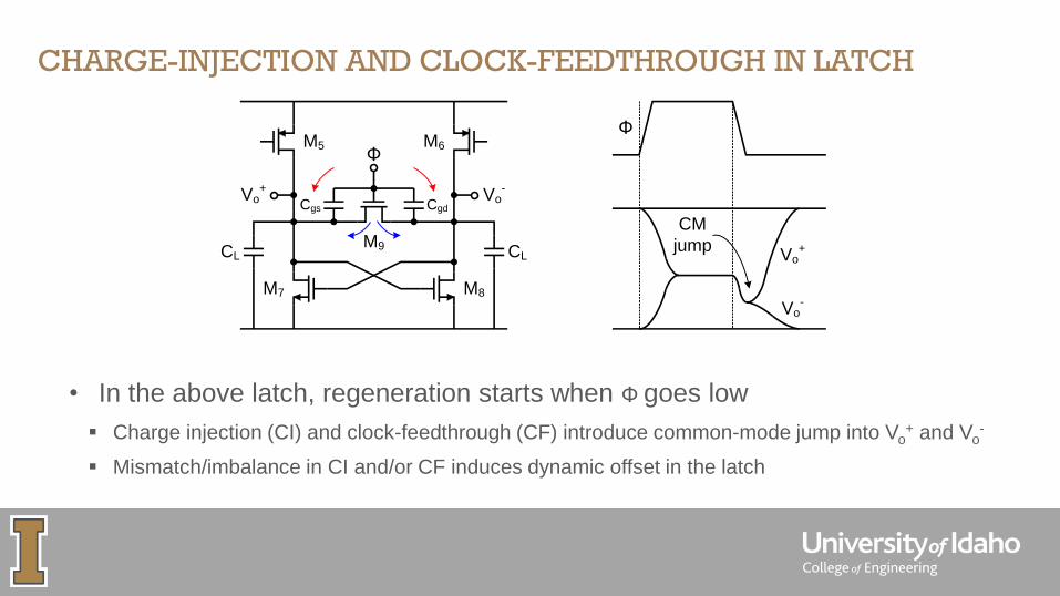
CHARGE-INJECTION AND CLOCK-FEEDTHROUGH IN LATCH
Reg. Speed – Linear ModelM5 M6
M8M7
Φ
Vo+
Vo-
CL CLM9
CgdCgs
Vo+
Vo-
Φ
CM
jump
• In the above latch, regeneration starts when Φ goes low
Charge injection (CI) and clock-feedthrough (CF) introduce common-mode jump into Vo+ and Vo
-
Mismatch/imbalance in CI and/or CF induces dynamic offset in the latch

DYNAMIC AND STATIC OFFSETS IN A LATCHReg. Speed – Linear Model
Dynamic offset induced due to:
• Imbalanced CI and CF
• Imbalanced load capacitance
Static offset induced due to:
• Mismatch in the cross-coupled pairs
• Mismatch in the signal input circuitry
Φ
Vo+
Vo-
offset50mV imbalance 10%
jump CM0.5V
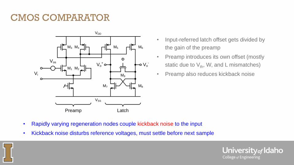
CMOS COMPARATORReg. Speed – Linear Model
• Input-referred latch offset gets divided by
the gain of the preamp
• Preamp introduces its own offset (mostly
static due to Vth, W, and L mismatches)
• Preamp also reduces kickback noiseM1 M2
Vi
Vos
M3 M4
VDD
M5 M6
M8M7
M9
VSS
Φ
Vo+
Vo-
Preamp Latch
• Rapidly varying regeneration nodes couple kickback noise to the input
• Kickback noise disturbs reference voltages, must settle before next sample

COMPARATOR OFFSETReg. Speed – Linear Model
M1 M2
Vi
Vos
M3 M4
VDD
M5 M6
M8M7
M9
VSS
Φ
Vo+
Vo-
Preamp Latch
L
L
2
22 2
os th ov
WΔ
1V ΔV V
W4
9m7
9m5V2
Rg2
RgA
m3
m1V1
g
gA
2
V2
2
V1
2
dynos,
2
V2
2
V1
2
os,78
2
V1
2
os,56
2
os,342
os,12
2
osAA
V
AA
V
A
VVVV
Differential pair mismatch:
Total input-referred
comparator offset:

REVIEW: TRANSISTOR MATCHINGReg. Speed – Linear Model
,DSWL
AΔPσ 22
P
2
P2
Suppose parameter P of two rectangular devices has a mismatch error of ΔP. The
variance of parameter ΔP b/t the two devices is
where, W and L are the effective width and length, D is the distance
Ref: M. J. M. Pelgrom, et al., “Matching properties of MOS transistors,” IEEE Journal of Solid-State Circuits, vol. 24, pp. 1433-1439, issue 5, 1989.
22 2 2Vth
th Vth
22β 2 2
β2
AThreshold: σ V = +S D
WL
Aσ βCurrent factor : S D
β WL
1st term dominates
for small devices

RECALL: DEVICE SIZING FOR MISMATCHReg. Speed – Linear Model
1 S R1
LR R with std σ
W
X X X X X X X X…W
L10 identical resistors
R1 R2
R2 R1 R1 R
2 1 1
σ 10σ σ σ1 1 1
R 10R R R10 A WL
j
2 S 1 R2
102 2 2
R2 R R1 R2 R1
j 1
LR R 10 10R with std σ ,
W
σ σ 10σ σ 10σ
“Spatialaveraging”

PRE-AMP DESIGN
A fully-differential gain-stage
Avoid or use simple CMFB
Pre-amp gain reduces input referred offset due to the latch
Autozero techniques for offset storage and reduction
Pre-amp open-loop gain vs tracking bandwidth trade-off
Multiple stages of pre-amp limit bandwidth
Optimum value of stages 2-4
NN
0 0N
20
0
1N
0 NN 3dB 3dB 0
A AA ω
1 j ω /ω 1 ω /ω
AA ω ω , ω ω 2 1
2
N stages:

PRE-AMP (PA) AUTOZERO
A
VosΦ1
Φ2
Φ2'
Vi Vo
C
M1 M2
M3 M4
Vi+
Vi-
M5
Vo+
Vo-
Φ2'
M6
,
,
OS pre amp
OS inA
Finite preamp gain :
VV
, ,
,
2 2
2
2 2
1
OS pre OS Latch
OS in
prepre
AA
V V
V
For the overall comparator :

PRE-AMP DESIGN: PULL-UP LOAD
• NMOS pull-up suffers from body-effect, affecting gain accuracy
• PMOS pull-up is free from body-effect, but subject to P/N mismatch
• Gain accuracy is the worst for resistive pull-up as resistors (poly, diffusion, well, etc.) don’t track transistors; but it is
fast!
M1 M2Vi+
Vi-
Vo+
Vo-
Pull-up
L
1
mL
m1V
LW
LW
g
gA
:uppull diode NMOS
L
1
p
n
mL
m1V
LW
LW
μ
μ
g
gA
:uppull diode PMOS
Lm1V RgA
:uppull Resistor

PRE-AMP DESIGN: MORE GAIN
• Ip diverts current away from PMOS diodes (M3 & M4), reducing (W/L)3
• Higher gain without CMFB
• Needs biasing for Ip
• M3 & M4 may cut off for large Vin, resulting in a slow recovery
M1 M2
M3 M4
Vi+
Vi-
Vo+
Vo-
Ip Ip
I
3
1
pp
n
m3
m1V
LW
LW
I2I
2I
μ
μ
g
gA
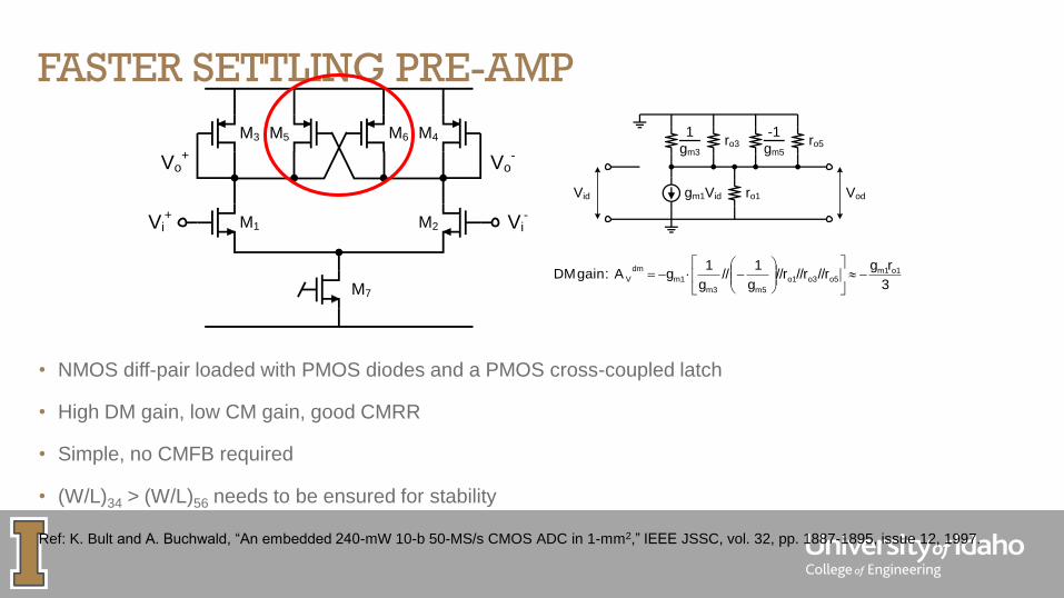
FASTER SETTLING PRE-AMP
• NMOS diff-pair loaded with PMOS diodes and a PMOS cross-coupled latch
• High DM gain, low CM gain, good CMRR
• Simple, no CMFB required
• (W/L)34 > (W/L)56 needs to be ensured for stability
Ref: K. Bult and A. Buchwald, “An embedded 240-mW 10-b 50-MS/s CMOS ADC in 1-mm2,” IEEE JSSC, vol. 32, pp. 1887-1895, issue 12, 1997.
M1 M2
M7
M3 M4
Vi+
Vi-
Vo+
Vo-
M5 M6
Vid gm1Vid ro1
1
gm3ro3
-1
gm5ro5
Vod
3
rg//r//r//r
g
1//
g
1g A:gain DM o1m1
o5o3o1
m5m3
m1
dm
V

PRE-AMP EXAMPLE
• NMOS diff. pair loaded with PMOS diodes and resistors
• High DM gain, low CM gain, good CMRR
• Simple, no extra CMFB required
• Gain not well-defined
Ref: B.-S. Song et al., “A 1 V 6 b 50 MHz current-interpolating CMOS ADC,” in IEEE Symp. VLSI Circuits, 1999, pp. 79-80.
M1 M2
M5
M4M3
Vi+
Vi-
Vo+
Vo-
RL RL
X

PRE-AMP EXAMPLE
NMOS diff. pair loaded with PMOS Current mirror
Simple CMFB circuit using triode PMOS
Large DM gain, small CM gain
Ref: V. Srinivas, S. Pavan, A. Lachhwani, and N. Sasidhar, “A Distortion Compensating Flash Analog-to-Digital Conversion
Technique," IEEE JSSC, vol. 41, no. 9, pp. 1959-1969, Sep. 2006.

LATCH DESIGN• Regenerative latches for faster settling
• See lecture notes
• At least one cross-coupled regenerative core
• Numerous methods for applying the input initial signal for regeneration
• Latches can have large static and dynamic offsets
• Large Regenerative gain for resolving small inputs
• Metastability (wrong or incomplete decisions) when latch can’t make decision
• Pre-amp used for larger gain (slower tracking BW)
• One topology doesn’t fit all the applications
• Speed vs power consumption trade-off
STATIC LATCH EXAMPLE
• Active pull-up and pull-down
• full CMOS logic levels
• Very fast!
• Q+ and Q- are not well defined in reset mode (Φ = 1)
• Large short-circuit current in reset mode
• Zero DC current after full regeneration
• Supply is very noisyM6M5
M7
Q+
Q-
Φ
Vi+
Vi-
M1 M2
M3 M4

SEMI-DYNAMIC LATCH EXAMPLE
M6M5
M7
Φ
Φ
M8
Vi+
Vi-
M1 M2
M3 M4
Q+
Q-
• Latch is disabled in reset mode
• less static current
• Pull-up not as fast
• Q+ and Q- are still not well defined in reset mode (Φ
= 1)
• Zero DC current after full regeneration
• Supply still very noisy

DYNAMIC LATCH EXAMPLE
M4M3
Φ
Vi+
Vi-
M7 M8M5 M6
M1
Q+
Q-
M2
M9 M10 Φ
ΦΦ
• Zero DC current in reset mode
• Q+ and Q- are both reset to “0”
• Full logic level after regeneration
• Slow

DYNAMIC LATCH EXAMPLE 2
Φ
Vi+
Vi-
M7 M8M5 M6
M1
Q+
Q-
M2
M9 M10 Φ
ΦΦ
M4M3
• Zero DC current in reset mode
• Q+ and Q- are both reset to “0”
• Full logic level after regeneration
• Slow
Ref: T. B. Cho and P. R. Gray, “A 10 b, 20 Msample/s, 35 mW pipeline A/D converter,” JSSC, vol. 30, pp. 166-172, issue 3, 1995.

CURRENT-STEERING/CML LATCH
• Current mode logic (CML) latch
• Constant bias current
• supply very quite
• Higher gain in tracking mode
• Cannot produce full logic levels
• Fast
• Popular for high-speed designs

COMPARATOR WITH PA AUTOZERO
I. Mehr and L. Singer, “A 55-mW, 10-bit, 40-Msample/s Nyquist-Rate CMOS ADC,” IEEE JSSC March 2000, pp. 318-25.

LOW-POWER LATCH WITH REFERENCE SUBTRACTION
S. Pavan, N. Krishnapura, R. Pandarinathan, P. Sankar, "A Power Optimized Continuous-time Delta-Sigma Modulator for Audio Applications," IEEE JSSC, vol. 43, no. 2,
pp. 351-360, Feb. 2008.
• Energy efficient comparator for medium speed data converters
• Large number of clock phases
• Driving and routing at higher clock rates leads to more power consumption
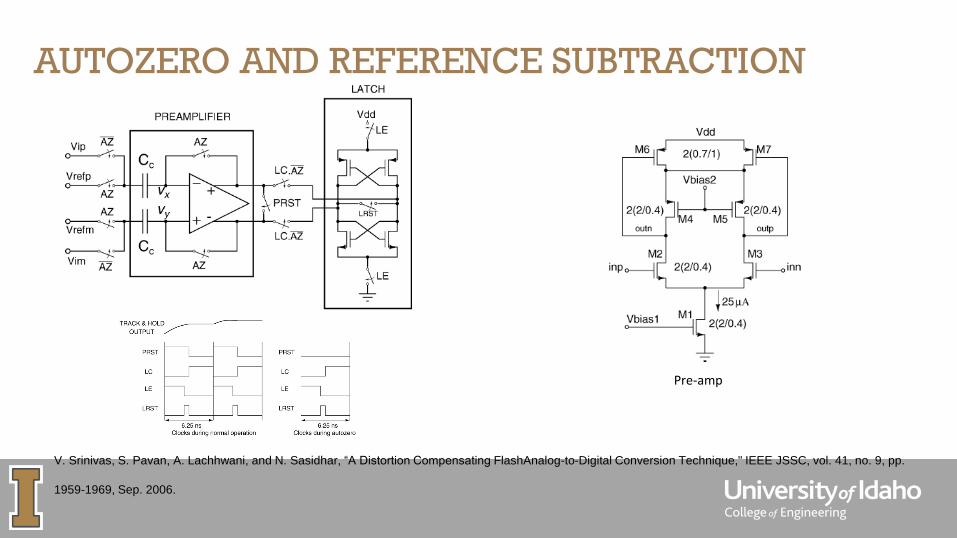
AUTOZERO AND REFERENCE SUBTRACTION
V. Srinivas, S. Pavan, A. Lachhwani, and N. Sasidhar, “A Distortion Compensating FlashAnalog-to-Digital Conversion Technique," IEEE JSSC, vol. 41, no. 9, pp.
1959-1969, Sep. 2006.
Pre-amp
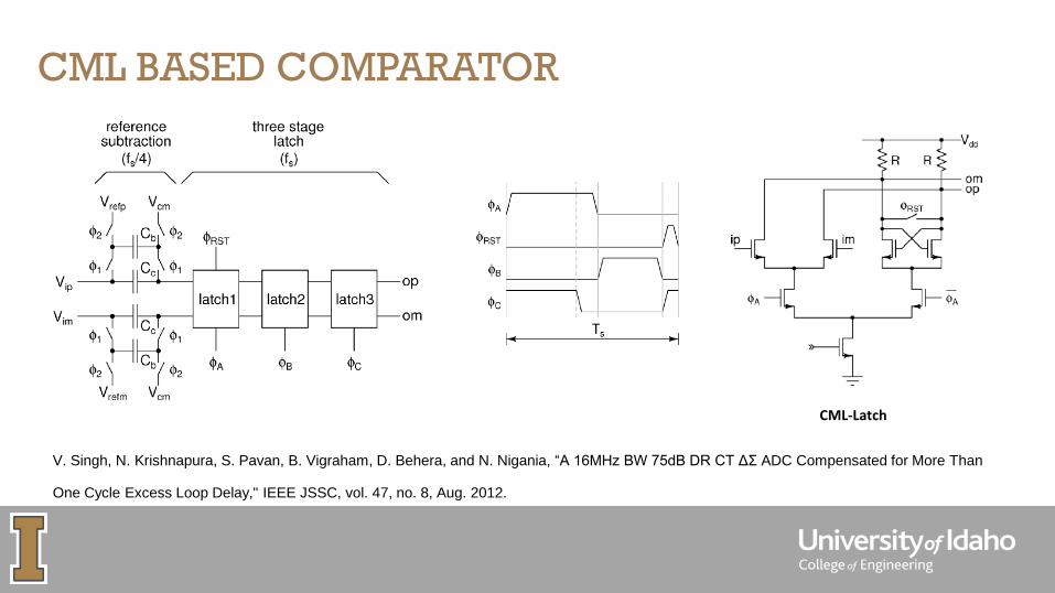
CML BASED COMPARATOR
V. Singh, N. Krishnapura, S. Pavan, B. Vigraham, D. Behera, and N. Nigania, “A 16MHz BW 75dB DR CT ΔΣ ADC Compensated for More Than
One Cycle Excess Loop Delay," IEEE JSSC, vol. 47, no. 8, Aug. 2012.
CML-Latch

COMPARATORS FOR PIPELINED ADCS
• Pipelined ADCs employ at least 0.5 bit/stage redundancy
Can tolerate large offsets and large noise with appropriate redundancy
• Should consume negligible power in a good design
• 50-100 μW or less per comparator
• Lots of implementation options
Resistive/capacitive reference generation
Different pre-amp/latch topologies

COMPARATORS FOR PIPELINED ADCS

COMPARATOR EXAMPLE
A 6-b 1.3-Gsample/s A/D Converter in 0.35-m CMOS IEEE JSSC, vol. 36, no. 12, Dec 2001.

LATCH EXAMPLE
A 0.9-V 60-W 1-Bit Fourth-Order Delta-Sigma Modulator With 83-dB Dynamic Range IEEE JSSC, vol. 43,
no. 2, Feb. 2008

COMPARATOR EXAMPLE
A 77-dB Dynamic Range, 7.5-MHz Hybrid Continuous-Time/Discrete-Time Cascaded ΔΣ Modulator, IEEE
JSSC, vol. 43, no. 4, Apr 2008

COMPARATOR EXAMPLE
I. Galdi, 40 MHz IF 1 MHz Bandwidth Two-Path Bandpass ΣΔ Modulator With 72 dB DR Consuming 16 mW, IEEE JSSC,
vol. 39, no. 8, pp. 1341–1346, Aug. 2004.

COMPARATOR EXAMPLE
Y. Chiu, P. R. Gray, and B. Nikolic, "A 14-b 12-MS/s CMOS pipeline ADC with over 100-dB SFDR," IEEE JSSC, vol. 39, pp.
2139 - 2151, December 2004.

COMPARATOR EXAMPLE
B. Min, P. Kim, F. W. Bowman, D. M. Boisvert, and A. J. Aude, "A 69-mW 10-bit 80-MSample/s pipelined CMOS ADC,"
IEEE JSSC, vol. 38, pp. 2031 - 2039, Dec. 2003.
COMPARATOR EXAMPLE
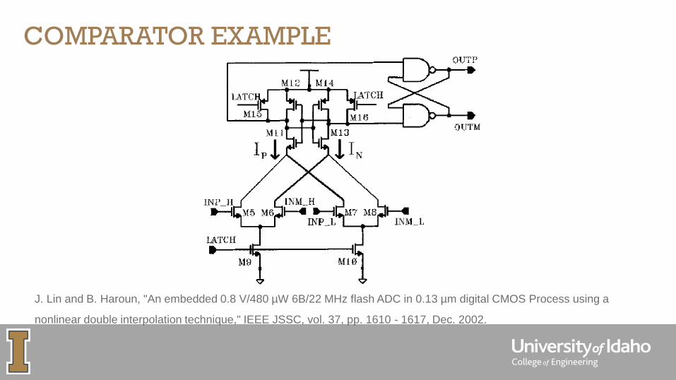
J. Lin and B. Haroun, "An embedded 0.8 V/480 µW 6B/22 MHz flash ADC in 0.13 µm digital CMOS Process using a
nonlinear double interpolation technique," IEEE JSSC, vol. 37, pp. 1610 - 1617, Dec. 2002.

COMPARATOR EXAMPLE
S . Limotyrakis, S. D. Kulchycki, D. Su, and B. A. Wooley, "A 150MS/s 8b 71mW time-interleaved ADC in 0.18µm CMOS,"
proc. IEEE ISSCC, pp. 258 - 259, Feb 2004.

EXERCISE
Compare the latches with respect to
Static power dissipation
Dynamic and Static Offsets
Kickback noise at the input
Number of clock phases
Maximum achievable clock speed

REFERENCES
1. Rudy van de Plassche, “CMOS Integrated Analog-to-Digital and Digital-to-Analog Converters,” 2nd Ed., Springer,
2005.
2. Y. Chiu, Data Converters Lecture Slides, UT Dallas 2012.
3. N. Krishnapura, Analog IC Design Lectures, IIT Madras, 2008.
4. B. Boser, Analog-Digital Interface Circuits Lecture Slides, UC Berkeley 2011.