Embed Size (px)
Citation preview

City, University of London Institutional Repository
Citation: Agrawal, A., Oates, A. & Cabrera-Espana, F. (2014). Fabrication and characterisation of Si micropillar PV structures. Materials Research Innovations, 18(7), pp. 500-504. doi: 10.1179/1433075X14Y.0000000244
This is the accepted version of the paper.
This version of the publication may differ from the final published version.
Permanent repository link: http://openaccess.city.ac.uk/5178/
Link to published version: http://dx.doi.org/10.1179/1433075X14Y.0000000244
Copyright and reuse: City Research Online aims to make research outputs of City, University of London available to a wider audience. Copyright and Moral Rights remain with the author(s) and/or copyright holders. URLs from City Research Online may be freely distributed and linked to.
City Research Online: http://openaccess.city.ac.uk/ [email protected]
City Research Online

Fabrication and Characterisation of Si Micro-Pillar PV Structures
A Oates*, F J Cabrera-España, A Agrawal and H S Reehal London South Bank University, 103 Borough Road, London SE1 0AA, UK
City University London, Northampton Square, London, EC1V 0HB, UK
* Corresponding Author [email protected], 020 7815 7509
Arrays of vertical silicon micro pillar radial junction solar cells have been fabricated by diffusion of direct application spin on dopant and from the vapour phase through proximity rapid thermal diffusion. The micro pillars were fabricated by optical lithography and deep reactive ion etching.
The micro pillar arrays show superior anti-reflective properties over the measured spectrum and good correlation to finite difference time domain modelling of identical geometry arrays.
Junctions formed by a conventional spin on doping process of phosphorus containing dopant solution produced Suns-Voc values in the region of 0.3 V. This value is likely due to difficulties encountered in achieving an even distribution of dopant over the entire surface of the arrays.
An alternative method utilising spin on dopant but employing an intermediate vapour phase diffusion step produced promising results with Suns-Voc values reaching 0.5 V following a post diffusion drive in step.
Keywords: Silicon; Thin-film; Structured; Spin on doping; Rapid thermal diffusion
1. Introduction
The modern photovoltaic market continues to be dominated by tried and tested Si wafer based solar panels. Despite this, the overarching cost of the high quality Si required continues to be a limiting factor to overall market penetration. Thin film alternatives promise significant reductions in raw material requirements and the opportunity to deposit from the gas phase but suffer from poor efficiencies.
Structured Si solar cells are showing great promise as a means to enhance thin film cell performance and reduce the quantity and quality of raw material required. Vertically arrayed nano and micro scale pillars based on the radial junction geometry have two key advantages. First, they have reduced reflection compared to planar Si over a wide range of the optical spectrum [1]. Secondly, they decouple the photon absorption length from that of the carrier collection distance [2]. This relaxes the requirement for long carrier lifetimes and permits lower quality Si to be used which reduces material costs [3].
There has been significant work in the area of nano-scale structures prepared by a variety of techniques and covering much of the dimensional variable space. Structuring schemes of this scale demonstrate excellent anti-reflective and light trapping properties with light absorption values in the region of 99% being achievable [4].
The optical properties of such approaches are receiving significant attention, with the optimisation of dimensions and geometry for structures in the nano-scale being substantially addressed from a modelling approach. Some studies have indicated that disordered arrays may provide superior performance to

that of ordered structures [5], whilst others indicated that disordered location of nanostructures has a lesser effect on the absorbed spectrum [6].
Investigation of ordered arrays has demonstrated that structured silicon surfaces have significantly reduced reflection compared to planar silicon films of equivalent thicknesses. The studies indicate that the properties of the arrays are dependent on a variety of factors including the diameter and length of features, their periodicity and their surface filling fraction [7-10].
The majority of work reported on nano-scale structures previously has focused on their optical properties with less focus on electronic performance. That which has been carried out indicates the large surface area of nano arrays causes high surface recombination velocity with a corresponding reduction in charge carrier collection [11-12]. Effective doping of nano structures is also problematic with tight tolerances on dopant concentration and junction depth required to prevent carrier depletion [13].
Fewer studies have been carried out on micro-scale pillar structures, with those that have been undertaken being predominantly of the experimental approach and from an electronic point of view. Despite this, arrays of organised pillars with Voc values near 600mV have been demonstrated [14-15] which is a significant improvement over nano-scale structures. Junction formation by both grown and diffused emitter was undertaken and demonstrated the potential advantages to improved electronic performance of micro-scale structures.
We report optical characterisation of hexagonally arrayed vertical micro pillars prepared on single crystal p-type Si wafers as a model system for radial junction solar cells. Pillar formation was achieved by optical lithography and deep reactive ion etching (DRIE). Results are compared with finite difference time domain (FDTD) models of arrays with equivalent geometries. It is believed that this is the first systematic study of the optical properties of identically configured modelled and manufactured micro-scale pillars. Both methods demonstrated the superior anti-reflective properties of micro pillars to planar Si.
Results are also presented for initial junction formation by spin-on dopant based techniques and rapid thermal processing for dopant drive in, as measured by Suns-Voc. This technique employs photoconductance measurements to extract Suns-Voc and Implied Voc values for a cell allowing performance inference at a pre-contact stage to monitor the efficacy of process steps [16].
2. Modelling
The likely enhancement of the proposed structures was studied using the FDTD technique [17]. A schematic of the simulation set up is shown in Fig 1.
A Si micro pillar array was placed on the surface of the modelled Si substrate. A plane wave source with a simulated spectrum identical to the reference solar spectrum AM 1.5 is used in the simulation. The reflectance was obtained from a plane monitor placed in parallel to the surface of the micro pillar arrays and above the plane wave source (receiving only reflected waves).
Fig 1 goes here

Perfectly Matched Layer (PML) boundary conditions [18] were applied above the source and below the array to terminate the numerical window and absorb any stray radiation. However, on the remaining boundaries (i.e. the edges of the array) Periodic Boundary Conditions (PBC) were applied. By applying this type of boundary condition, an infinite array of micro pillars is simulated.
The parameters to be varied for these simulations were: micro pillar height, diameter and inter-pillar spacing.
3. Experimental
The Si micro pillars were prepared by stepper reticle optical lithography followed by a DRIE process. Briefly, this utilises a 1:5 scale reticle mask which is projected through a reduction lens onto the resist coated wafer. The reticle is stepped across the surface by a high resolution aligner to project the pattern over the desired area and match it to previously patterned areas. The starting wafer was of p-type (boron doped) with a resistivity in the range 0.1-0.5 Ωcm.
Pillars of 1 µm and 10 µm diameter were prepared with aspect ratios of 1:1 and 2:1 and edge to edge spacing of 0.5 µm, 0.75 µm and 1 µm for the 1 µm pillars and 2.5 µm, 5.0 µm, 7.5 µm and 10 µm for the 10 µm pillars. Due to hardware limitations, it was not possible to achieve samples with 1 µm diameter and 0.25 µm spacing.
The pillars were arrayed hexagonally as this increased the total surface populated by pillars from approximately 40% for a square arrangement to nominally 47%. Comparative modelling and literature indicated that there was little demonstrable effect on the light trapping properties of the array between the two arrangements [19].
Samples with patterned areas of size 81 mm2 and 324 mm2 were prepared. The larger samples were necessary for optical characterisation whilst the reduced area of the smaller samples minimised the likelihood of defects during junction formation.
Examination of a selection of arrays under SEM revealed negligible etching defects and well defined structures. The image shown (Fig 2) is representative of all the arrays observed. The characteristic undulating side wall produced by the DRIE process is clearly visible with a larger feature approximately half way down the pillars. This is a result of the change in the etch recipe to maintain the aspect ratio of the pillars.
Fig 2 goes here
After pillar fabrication, samples were submersed in a bath of ultrasonically agitated acetone then rinsed in running de-ionised (DI) water and dried under nitrogen (N2). A piranha etch (3:1 – H2SO4:H2O2) was carried out to remove organic contamination followed by a second DI rinse and N2 dry. The arrays were then etched in 2% Hydrofluoric Acid (HF) to remove the native oxide.
Initial junction formation was carried out using a phosphorus containing spin on dopant solution (SOD, from Filmtronics Inc). This was applied to the pillar arrays whilst stationary, followed by a 30 second spin at 5000rpm to distribute a thin layer of doped solution across the surface. The samples were then baked at 200°C for 10 minutes to drive off the solvent carrier leaving a doped

glassy oxide. Drive in was carried out at 900°C, 950°C and 1000°C by rapid thermal diffusion (RTD) for 30 seconds. Samples were then removed and subjected to a 49% HF etch to remove the residual oxide layer followed by characterisation using Suns-Voc.
Due to difficulties encountered in attaining an even distribution of dopant over samples resulting from the non-planar surface, an alternative method of doping was also evaluated referred to as proximity rapid thermal diffusion (P-RTD) [20]. A p-type <111> Si wafer was acetone cleaned and piranha etched to produce a hydrophilic surface. A layer of the same SOD solution used previously was then spun onto the surface and the wafer baked at 200°C for 10 minutes to drive off excess solvent. This was then placed facing the samples to be doped with a gap of 0.5 mm in a rapid thermal processing (RTP) system (Fig 3). The assembly was heated to 1050°C for 30 seconds in an N2 ambient resulting in out-diffusion of phosphorus from the doped oxide layer to its surface.
Fig 3 goes here
The phosphorus evaporates and is carried by gas phase diffusion to the surface of samples opposite. At the sample surface, adsorption takes place resulting in a reduction of the dopant oxide and oxidation of the silicon surface [21]. From this point the process is similar to that of conventional spin on doping with phosphorus atoms diffusing into the Si lattice. The P-RTD process is essentially similar to chemical vapour deposition (CVD) but utilising a solid phase dopant source rather than gaseous precursors. As the source is limited by the dopant available from the source wafer, the efficiency of the doping process is dependent on the properties of the source doped oxide film.
After diffusion and unloading from the RTP system, samples were etched in 49% HF to remove residual dopant from the surface. To improve uniformity of dopant distribution and increase the junction depth the samples were then annealed in a tube furnace at 1100°C for 15 minutes.
4. Results and Discussion
Optical characteristics of the pillar arrays, specifically their reflectance, were characterised by a Varian Carey 500 Scan UV-Vis-NIR Spectrophotometer. Measurements were taken using a monochromated probe beam with wavelength stepped in 1nm increments in the range 300-1100nm. The reflected light was collected by an integrating sphere with a silicon photo detector. The sample was mounted such that the angle of incidence of the probe beam was 3 degrees off normal. This allowed for both specular and diffused reflected light to be captured rather than the specular reflectance being lost back through the beam aperture.
Shown in Fig 4 is the reflectance of the 1 μm diameter, 2 μm length pillar arrays. It is apparent that for all values of pillar spacing there is a reduction of between 20-30% reflection across the measured spectrum compared to the planar sample. Further to this, it is generally the case that as the spacing between the pillars decreases, so too does the total reflection.
Fig 4 goes here

It is also noted that all of the samples show a slight reduction in reflection around the 1000 nm (1 μm) mark suggesting an effect of the pillar diameter on the equivalent wavelength.
The reflectance data for the 10 μm diameter, 20 μm length pillars for all values of spacing is shown in Fig 5. All samples show improvement over the planar wafer sample on the order of 5-15%.
It should be noted that the reduction in reflection between the 7.5 μm and 10 μm samples is reduced compared to the other values. This suggests that values exceeding 10 μm are unlikely to provide significant anti-reflective enhancement beyond that which results from surface roughening inherent to the DRIE process.
Fig 5 goes here
A comparison of measured reflectance data and that produced by the FDTD modelling is shown in Fig 6. The upper trace is a measured profile of the reflectance of a planar silicon sample compared to the model’s interpretation of the reflectance of an equivalent simulated sample. Good correlation is seen across the majority of the spectrum which indicated that the initial conditions were appropriate. The lower trace compares the modelled and measured data of a pillar array sample with a similar level of agreement. Whilst all array geometries demonstrate similar modelled and measured profiles, it has been observed that the arrays of 2 μm length pillars exhibit superior correlation.
Also of note is the oscillation that is present in the modelled reflection profiles. A hypothesis for this is that the space between the pillars acts as a cavity with a complex shape and there may be resonances set up which cause dips in the reflection properties. Running the simulations with a range of different mesh sizes does not lead to differences in the modelled spectra suggesting mesh discretisation errors are not responsible. Further work is to be undertaken to better understand this effect.
Fig 6 goes here
Electronic measurements were carried out using the Suns-Voc technique [22]. This uses a light flash from a xenon lamp, with the quasi steady-state open circuit voltage (Voc) being measured as a function of decreasing light intensity from the flash. As Voc is directly measured rather than the short-circuit current, it is generally accepted that the contact of a sharp tipped probe is an adequate contact [16]. As such no additional contacting was applied post junction formation.
To obtain implied or pseudo I-V curves from the Suns-Voc technique, a value for the short circuit current density (Jsc) is required. Unless a complete contacted cell is produced and characterised under a conventional AM1.5(G) solar I-V tester then this must be approximated. In this case, the value of 15mA/cm2 was assumed. This was an approximation based on measured Jsc values from a variety of previously produced complete test cells. Even with an accurate value for Jsc the I-V curved extracted from the Suns-Voc data would be at the upper bound for performance as the technique does not take into account the series resistance of the cell. Indeed, by comparing the Suns-Voc of a cell and the measured I-V curve a precise value for series resistance may be determined.

Fig 7 illustrates the effect of diffusion temperature on the resulting Suns-Voc of pillar cells diffused directly from a layer of spin on dopant. Also shown is the calculated junction depth for each diffusion temperature.
An improvement in Suns-Voc is observed between 900°C and 950°C which is followed by a significant decrease at 1000°C. This may be explained by the exponential increase in the diffusion co-efficient of phosphorus with temperature and the limited supply of dopant. As the diffusion source is limited, the substantial increase in junction depth (and associated dopant consumption) at 1000°C could result in source dopant depletion. In this event the existing dopant would be distributed more sparsely, resulting in an inadequately doped n-type region. An alternative possibility is poor doping uniformity resulting from the spin on process. Despite producing a hydrophilic surface on the pillar samples, ultimately the surfaces are non-planar and achieving a conformal distribution of dopant is challenging. The potential result is a junction with poor uniformity and corresponding low performance.
Attempts were made to increase the total dopant concentration available from the spun on solution by repeated applications. This approach showed some potential but resulted in poor uniformity of distribution as the hydrophilic surface required for even coverage is lost after the initial application.
Fig 7 goes here
Fig 8 illustrates the Suns-Voc I-V curves from a pillar array immediately after P-RTD and following a 15 minute 1100°C dopant drive in process. After the initial diffusion, a shallow and highly doped n-type region exists resulting in a Suns-Voc value of 0.118 V. The subsequent drive in step distributes the dopant more deeply, forming an improved junction and resulting in a dramatically improved Suns-Voc value of 0.526 V.
Fig 8 goes here
5. Conclusions
In conclusion, pillar arrays on the micron scale with various geometries have been demonstrated to produce superior optical properties to planar Si. Good agreement was found with FDTD models of identical geometry arrays which provide a solid basis for further predictive analysis of as yet unrealised pillar array formations.
The formation of p-n junctions on the arrays by direct spin on doping produced a measurable junction with Suns-Voc values in the region of 0.3 V. Difficulty was encountered in evenly distributing the dopant over the entire structured area of the samples due to the non-planar surface. The resultant variation in Suns-Voc across the surface suggested that the inconsistent dopant uniformity resulted in an unevenly distributed junction with poor overall performance as a consequence.
Following the initial P-RTD step, Suns-Voc values in the region of 0.1 V were obtained. A post diffusion drive in step improved this substantially to over 0.5 V. This suggests that a suitable concentration of dopant is diffused during the initial P-RTD process but insufficient thermal energy is imparted upon the samples to effectively distribute the phosphorus into the Si lattice. It is possible that a multi-step RTD process with high initial temperatures for

effective gas phase diffusion followed by a longer period at a lower temperature for dopant drive in may eliminate the need for the separate thermal process. The improvement in Suns-Voc compared to the conventional SOD process is likely due to more the even distribution of dopant over the entire array area and corresponding improvement in junction formation.
6. Acknowledgements
Thanks are due to Philips Innovation Services for pillar preparation and the EUMINAFAB open access scheme for funding. Dr R Minev is thanked for helpful discussions.
A. Oates further wishes to thank the EPSRC for funding.
7. References
1. C. Lin and M. Povinelli: ‘Optical absorption enhancement in silicon nanowire arrays with large lattice constant for photovoltaic applications’, Opt. Express, 2009, 17, (22), 19371-19381.
2. M. D. Kelzenberg, S. W. Boettcher, J. A. Petykiewicz, D. B. Turner-Evans, M. C. Putnam, E. L. Warren, J. M. Spurgeon, R. M. Briggs, N. S. Lewis and H. A. Atwater: ‘Enhanced absorption and carrier collection in Si wire arrays for photovoltaic applications’, Nat. Mater., 2010, 9, 239-244.
3. B. M. Kayes, N. S. Lewis and H. A. Atwater: ‘Comparison of the device physics principles of planar and radial p-n junction nanorod solar cells’, J. Appl. Phys., 2005, 97, (11), 114302.
4. J-Y. Jung, H-D. Um, S-W, Jee, K-T. Park, J H Bang and J-H Lee: ‘Optimal design for antireflective Si nanowire solar cells’, Sol. Energ. Mat. Sol. Cells., 2013, 112, 84-90.
5. H. Bao and X. Ruan: ‘Optical absorption enhancement in disordered vertical silicon nanowire arrays for photovoltaic applications’, Opt. Lett., 2010, 35, (20), 3378-3380.
6. N. Lagos, M.M. Sigalas and D. Niarchos: ‘The optical absorption of nanowire arrays’, Phot. Nano. Fund. Appl., 2011, 9, 163-167.
7. L. Hu and G. Chen: ‘Analysis of optical absorption in silicon nanowire arrays for photovoltaic applications’, Nano. Lett., 2007 7, (11), 3249-3252.
8. J. Li, H. Y. Yu, S. M. Wong, X. Li, G. Zhang, P. G-Q. Lo, and D-L. Kwong: ‘Design guidelines of periodic Si nanowire arrays for solar cell application’, Appl. Phys. Lett., 2009, 95, 243113.
9. J. Kupec, R. L. Stoop, and B. Witzigmann: ‘Light absorption and emission in nanowire array solar cells’, Opt. Express, 2010, 18, (26), 27589-27605.
10. Z. Duan, M. Li, T. Mwenya, F. Bai, Y. Li and D. Song: ‘Geometric parameter optimization to minimise the light-reflection losses of regular vertical silicon nanorod arrays used for solar cells’, Phys. Status Solidi a, 2014, DOI 10.1002/pssa.201431189.
11. F. Toor, H.M. Branz, M.R. Page, K.M. Jones and H-C. Yuan: ‘Multi-scale surface texture to improve blue response of nanoporous black silicon solar cells’, Appl. Phys. Lett., 2011, 99, 103501.
12. H. Li, R. Jia, C. Chen, Z. Xing, W. Ding, Y. Meng, D. Wu, X. Liu and T. Ye: ‘Influence of nanowires length on performance of crystalline silicon solar cell’, Appl. Phys. Lett., 2011, 98, 151116.

13. Z. Li, J. Wang, N Singh and S. Lee: ‘Optical and electrical study of core-shell silicon nanowires for solar applications’, Opt. Express, 2011, 19, (S5), A1057-A1066.
14. M. Gharghi, E. Fathi, B. Kante, S. Sivoththaman and X. Zhang: ‘Heterojunction silicon microwire solar cells’, Nano Lett., 2012, 12, (12), 6278-6282.
15. H. Kim, J. Kim, E. Lee, D-W. Kim, J-H. Yun and J. Yi: ‘Effect of the short collection length in silicon microscal wire solar cells’, Appl. Phys. Lett., 2013, 102, 193904.
16. R. A. Sinton, A. Cuevas and M. Stuckings: ‘Quasi-steady-state photoconductance, a new method for solar cell material and device characterisation’, Proc. of the 25th Photovoltaic Specialists Conference, Washington, D.C., USA, May 1996, 457-460.
17. K. Yee: ‘Numerical Solution of Initial Boundary Value Problems Involving Maxwell’s Equations in Isotropic Media’, IEEE Trans. Antennas Propagat., 1966, 14, (5) 302-307.
18. J. Berenger: ‘A Perfectly Matched Layer for the Absorption of Electromagnetic Waves’, J. Comput. Phys., 1994, 114, 185-200.
19. J. Li, H. Yu and Y. Li: ‘Solar energy harnessing in hexagonally arranged Si nanowire arrays and effects of array symmetry on optical characteristics’, Nanotechnology, 2012, 23, (19).
20. W. Zagozdzon-Wosik, J. C. Wolfe and C. W. Teng: ‘Doping of trench capacitors by rapid thermal diffusion’, IEEE Trans. Electron Device Lett., 1991, 12, (6), 264-266.
21. J. R. Flemish, R. E. Tressler and J. Ruzyllo, ‘Phosphorus diffusion in silicon from enclosed solid planar sources’, J. Electrochem. Soc., 1991, 138, 205-207.
22. R. A. Sinton and A. Cuevas: ‘A quasi-steady-state open-circuit voltage method for solar cell characterization’, Proc. of the 16th European Photovoltaic Solar Energy Conference, Glasgow, UK, May 2000, 1152-1155.
Image Captions Fig 1. Representation of FDTD simulation configuration Fig 2. SEM image of 1 μm diameter, 2 μm length micro pillars at 1 μm spacing Fig 3. Equipment configuration for proximity rapid thermal diffusion Fig 4. Plot of 1 μm diameter, 2 μm length Si micro pillar reflectance with polished Si wafer sample for comparison Fig 5. Plot of 10 μm diameter, 20 μm length Si micro pillar reflectance with polished Si wafer sample for comparison Fig 6. Comparison of FDTD model and optical measurements of planar Si sample and 1 μm diameter, 2 μm length, 0.50 μm spaced pillars

Fig 7. Plot of open circuit voltage as a function of diffusion temperature and calculated junction depth based on diffusion conditions Fig 8. Suns-Voc results for 1 μm diameter, 1 μm length, 0.75 μm spacing pillar array after initial diffusion by P-RTD and following the post diffusion drive in step Figures
Figure 1
Figure 2
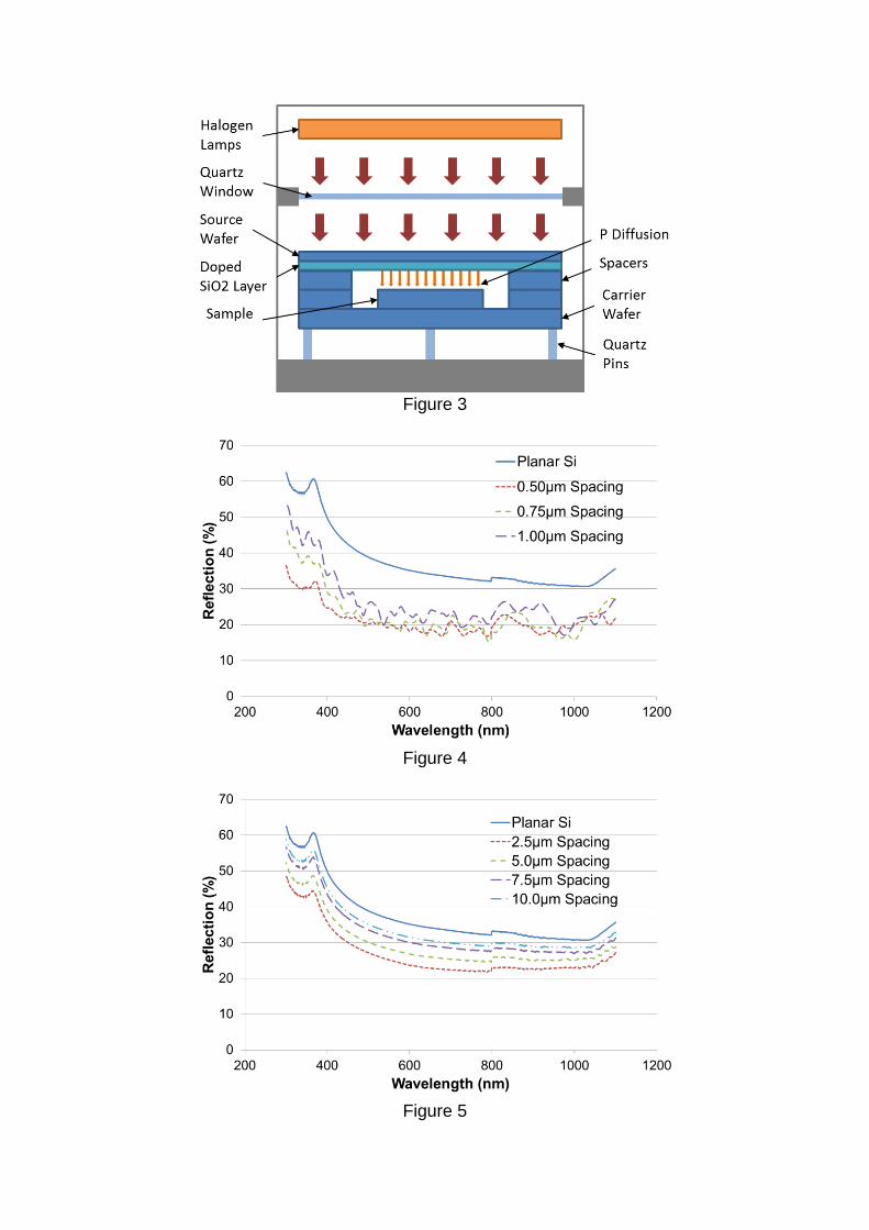
Figure 3
Figure 4
Figure 5

Figure 6
Figure 7
Figure 8