Embed Size (px)
Citation preview

M TC7660Charge Pump DC-to-DC Voltage Converter
Features• Wide Input Voltage Range: +1.5V to +10V• Efficient Voltage Conversion (99.9%, typ)• Excellent Power Efficiency (98%, typ)• Low Power Consumption: 80 µA (typ) @ VIN = 5V• Low Cost and Easy to Use
- Only Two External Capacitors Required• Available in 8-Pin Small Outline (SOIC), 8-Pin
PDIP and 8-Pin CERDIP Packages• Improved ESD Protection (3 kV HBM)• No External Diode Required for High-Voltage
Operation
Applications• RS-232 Negative Power Supply• Simple Conversion of +5V to ±5V Supplies• Voltage Multiplication VOUT = ± n V+
• Negative Supplies for Data Acquisition Systems and Instrumentation
Package Types
General DescriptionThe TC7660 is a pin-compatible replacement for theindustry standard 7660 charge pump voltageconverter. It converts a +1.5V to +10V input to acorresponding -1.5V to -10V output using only two lowcost capacitors, eliminating inductors and theirassociated cost, size and electromagnetic interference(EMI).The on-board oscillator operates at a nominalfrequency of 10 kHz. Operation below 10 kHz (forlower supply current applications) is possible byconnecting an external capacitor from OSC to ground.
The TC7660 is available in 8-Pin PDIP, 8-Pin SmallOutline (SOIC) and 8-Pin CERDIP packages incommercial and extended temperature ranges.
Functional Block Diagram
1
2
3
4
8
7
6
5
TC7660
NC
CAP+
GND
CAP- VOUT
LOW VOLTAGE (LV)
OSC
PDIP/CERDIP/SOIC
V+
TC7660
GND
InternalVoltage
Regulator
RCOscillator
VoltageLevel
Translator
V+CAP+
8 2
7
6
OSC
LV
3
LogicNetwork
VOUT5
CAP-4÷ 2
InternalVoltage
Regulator
2002 Microchip Technology Inc. DS21465B-page 1

TC7660
1.0 ELECTRICALCHARACTERISTICSAbsolute Maximum Ratings*Supply Voltage .............................................................+10.5VLV and OSC Inputs Voltage: (Note 1) .............................................. -0.3V to VSS for V+ < 5.5V .....................................(V+ – 5.5V) to (V+) for V+ > 5.5VCurrent into LV .........................................20 µA for V+ > 3.5VOutput Short Duration (VSUPPLY ≤ 5.5V)...............ContinuousPackage Power Dissipation: (TA ≤ 70°C) 8-Pin CERDIP ....................................................800 mW 8-Pin PDIP .........................................................730 mW 8-Pin SOIC.........................................................470 mWOperating Temperature Range: C Suffix.......................................................0°C to +70°C I Suffix .....................................................-25°C to +85°C E Suffix ....................................................-40°C to +85°C M Suffix .................................................-55°C to +125°CStorage Temperature Range.........................-65°C to +160°CESD protection on all pins (HBM) ................... ..............≥ 3 kVMaximum Junction Temperature ........... ....................... 150°C
* Notice: Stresses above those listed under "Maximum Rat-ings" may cause permanent damage to the device. This is astress rating only and functional operation of the device atthose or any other conditions above those indicated in theoperational sections of this specification is not intended. Expo-sure to maximum rating conditions for extended periods mayaffect device reliability.
FIGURE 1-1: TC7660 Test Circuit.
ELECTRICAL SPECIFICATIONS
123
4
876
5
TC7660+V+
(+5V)
VOUT
C110 µF
COSC
+C210 µF
IL
RL
IS
Electrical Characteristics: Unless otherwise noted, specifications measured over operating temperature range with V+ = 5V,COSC = 0, refer to test circuit in Figure 1-1.
Parameters Sym Min Typ Max Units Conditions
Supply Current I+ — 80 180 µA RL = ∞
Supply Voltage Range, High V+H 3.0 — 10 V Min ≤ TA ≤ Max, RL = 10 kΩ, LV Open
Supply Voltage Range, Low V+L 1.5 — 3.5 V Min ≤ TA ≤ Max, RL = 10 kΩ, LV to GND
Output Source Resistance ROUT — 70 100 Ω IOUT=20 mA, TA = +25°C— — 120 IOUT=20 mA, TA ≤ +70°C (C Device)— — 130 IOUT=20 mA, TA ≤ +85°C (E and I Device)— 104 150 IOUT=20 mA, TA ≤ +125°C (M Device)— 150 300 V+ = 2V, IOUT = 3 mA, LV to GND
0°C ≤ TA ≤ +70°C— 160 600 V+ = 2V, IOUT = 3 mA, LV to GND
-55°C ≤ TA ≤ +125°C (M Device)Oscillator Frequency fOSC — 10 — kHz Pin 7 open
Power Efficiency PEFF 95 98 — % RL = 5 kΩ
Voltage Conversion Efficiency VOUTEFF 97 99.9 — % RL = ∞
Oscillator Impedance ZOSC — 1.0 — MΩ V+ = 2V— 100 — kΩ V+ = 5V
Note 1: Destructive latch-up may occur if voltages greater than V+ or less than GND are supplied to any input pin.
DS21465B-page 2 2002 Microchip Technology Inc.
TC7660
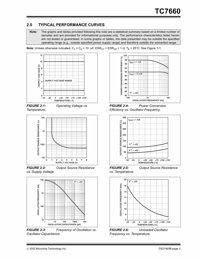
2.0 TYPICAL PERFORMANCE CURVESNote: Unless otherwise indicated, C1 = C2 = 10 µF, ESRC1 = ESRC2 = 1 Ω, TA = 25°C. See Figure 1-1.
FIGURE 2-1: Operating Voltage vs. Temperature.
FIGURE 2-2: Output Source Resistance vs. Supply Voltage.
FIGURE 2-3: Frequency of Oscillation vs. Oscillator Capacitance.
FIGURE 2-4: Power Conversion Efficiency vs. Oscillator Frequency.
FIGURE 2-5: Output Source Resistance vs. Temperature.
FIGURE 2-6: Unloaded Oscillator Frequency vs. Temperature.
Note: The graphs and tables provided following this note are a statistical summary based on a limited number ofsamples and are provided for informational purposes only. The performance characteristics listed hereinare not tested or guaranteed. In some graphs or tables, the data presented may be outside the specifiedoperating range (e.g., outside specified power supply range) and therefore outside the warranted range.
-25 0 +25 +75 +100 +125
12
10
8
6
4
2
+50-55
SU
PP
LY
VO
LT
AG
E (
V)
TEMPERATURE (°C)
0
SUPPLY VOLTAGE RANGE
7 8
10k
1k
100Ω
OU
TP
UT
SO
UR
CE
RE
SIS
TA
NC
E (
Ω)
6543210SUPPLY VOLTAGE (V)
10Ω
OSCILLATOR CAPACITANCE (pF)
10k
OS
CIL
LA
TO
R F
RE
QU
EN
CY
(H
z)
1
1k
100
1010 100 1000 10k
V+ = +5V
OSCILLATOR FREQUENCY (Hz)
100
PO
WE
R C
ON
VE
RS
ION
EF
FIC
IEN
CY
(%
)
98
96
92
90
88
86
84
82
80
94
100 1k 10k
V+ = +5V
IOUT = 1 mA
IOUT = 15 mA
500
450
400
200
150
100
50
0-55 -25 0 +25 +50 +75 +100 +125
TEMPERATURE (°C)
OU
TP
UT
SO
UR
CE
RE
SIS
TA
NC
E (
Ω)
V + = +2V
V + = +5V
IOUT = 1 mA
TEMPERATURE (°C)
OS
CIL
LA
TO
R F
RE
QU
EN
CY
(kH
z)
20
-55
18
16
14
12
10
8
6-25 0 +25 +50 +75 +100 +125
V+ = +5V
2002 Microchip Technology Inc. DS21465B-page 3

TC7660
Note: Unless otherwise indicated, C1 = C2 = 10 µF, ESRC1 = ESRC2 = 1 Ω, TA = 25°C. See Figure 1-1.FIGURE 2-7: Output Voltage vs. Output Current.
FIGURE 2-8: Supply Current and Power Conversion Efficiency vs. Load Current.
FIGURE 2-9: Output Voltage vs. Load Current.
FIGURE 2-10: Output Voltage vs. Load Current.
FIGURE 2-11: Supply Current and Power Conversion Efficiency vs. Load Current.
OUTPUT CURRENT (mA)
OU
TP
UT
VO
LT
AG
E (
V)
0
0
-1
-2
-3
-4
-5
-6
-7
-8
-9
-1010 20 30 40 50 60 70 80 90 100
LV OPEN
PO
WE
R C
ON
VE
RS
ION
EF
FIC
IEN
CY
(%
)
0 LOAD CURRENT (mA)
10
20
30
40
50
60
70
80
90
100
1.5 3.0 4.5 6.0 7.5 9.00
2
4
6
8
10
12
14
16
18
20
SU
PP
LY
CU
RR
EN
T (
mA
)
V+ = 2V
2
0
OU
TP
UT
VO
LT
AG
E (
V) 1
0
-1
-2 1 2 3 4 5 6 7 8
LOAD CURRENT (mA)
SLOPE 150Ω
V+ = +2V
LOAD CURRENT (mA)
OU
TP
UT
VO
LT
AG
E (
V)
1
0
5
4
3
2
0
-1
-2
-3
-4
-510 20 30 40 50 60 70 80
V+ = +5V
SLOPE 55Ω
LOAD CURRENT (mA)
PO
WE
R C
ON
VE
RS
ION
EF
FIC
IEN
CY
(%
)
0
10
20
30
40
50
60
70
80
90
100
0
10
20
30
40
50
60
70
80
90
100
SU
PP
LY
CU
RR
EN
T (
mA
)
10 20 30 40 50 60
V+ = +5V
DS21465B-page 4 2002 Microchip Technology Inc.
TC7660
3.0 PIN DESCRIPTIONSThe descriptions of the pins are listed in Table 3-1.TABLE 3-1: PIN FUNCTION TABLE
3.1 Charge Pump Capacitor (CAP+)Positive connection for the charge pump capacitor, orflying capacitor, used to transfer charge from the inputsource to the output. In the voltage-inverting configura-tion, the charge pump capacitor is charged to the inputvoltage during the first half of the switching cycle. Dur-ing the second half of the switching cycle, the chargepump capacitor is inverted and charge is transferred tothe output capacitor and load.It is recommended that a low ESR (equivalent seriesresistance) capacitor be used. Additionally, largervalues will lower the output resistance.
3.2 Ground (GND)Input and output zero volt reference.
3.3 Charge Pump Capacitor (CAP-)Negative connection for the charge pump capacitor, orflying capacitor, used to transfer charge from the inputto the output. Proper orientation is imperative whenusing a polarized capacitor.
3.4 Output Voltage (VOUT)Negative connection for the charge pump outputcapacitor. In the voltage-inverting configuration, thecharge pump output capacitor supplies the output loadduring the first half of the switching cycle. During thesecond half of the switching cycle, charge is restored tothe charge pump output capacitor.
It is recommended that a low ESR (equivalent seriesresistance) capacitor be used. Additionally, largervalues will lower the output ripple.
3.5 Low Voltage Pin (LV)The low voltage pin ensures proper operation of theinternal oscillator for input voltages below 3.5V. The lowvoltage pin should be connected to ground (GND) forinput voltages below 3.5V. Otherwise, the low voltagepin should be allowed to float.
3.6 Oscillator Control Input (OSC)The oscillator control input can be utilized to slow downor speed up the operation of the TC7660. Refer toSection 5.4, “Changing the TC7660 OscillatorFrequency”, for details on altering the oscillatorfrequency.
3.7 Power Supply (V+)Positive power supply input voltage connection. It isrecommended that a low ESR (equivalent series resis-tance) capacitor be used to bypass the power supplyinput to ground (GND).
Pin No. Symbol Description
1 NC No connection2 CAP+ Charge pump capacitor positive terminal3 GND Ground terminal4 CAP- Charge pump capacitor negative terminal5 VOUT Output voltage6 LV Low voltage pin. Connect to GND for V+ < 3.5V7 OSC Oscillator control input. Bypass with an external capacitor to slow the oscillator8 V+ Power supply positive voltage input
2002 Microchip Technology Inc. DS21465B-page 5

TC7660
4.0 DETAILED DESCRIPTION4.1 Theory of OperationThe TC7660 charge pump converter inverts the voltageapplied to the V+ pin. The conversion consists of a two-phase operation (Figure 4-1). During the first phase,switches S2 and S4 are open and switches S1 and S3are closed. C1 charges to the voltage applied to the V+
pin, with the load current being supplied from C2. Dur-ing the second phase, switches S2 and S4 are closedand switches S1 and S3 are open. Charge is trans-ferred from C1 to C2, with the load current beingsupplied from C1.
FIGURE 4-1: Ideal Switched Capacitor Inverter.In this manner, the TC7660 performs a voltage inver-sion, but does not provide regulation. The average out-put voltage will drop in a linear manner with respect toload current. The equivalent circuit of the charge pumpinverter can be modeled as an ideal voltage source inseries with a resistor, as shown in Figure 4-2.
FIGURE 4-2: Switched Capacitor Inverter Equivalent Circuit Model.The value of the series resistor (ROUT) is a function ofthe switching frequency, capacitance and equivalentseries resistance (ESR) of C1 and C2 and the on-resis-tance of switches S1, S2, S3 and S4. A closeapproximation for ROUT is given in the followingequation:
EQUATION
4.2 Switched Capacitor Inverter Power Losses
The overall power loss of a switched capacitor inverteris affected by four factors:
1. Losses from power consumed by the internaloscillator, switch drive, etc. These losses willvary with input voltage, temperature andoscillator frequency.
2. Conduction losses in the non-ideal switches.3. Losses due to the non-ideal nature of the
external capacitors.4. Losses that occur during charge transfer from
C1 to C2 when a voltage difference between thecapacitors exists.
Figure 4-3 depicts the non-ideal elements associatedwith the switched capacitor inverter power loss.
FIGURE 4-3: Non-Ideal Switched Capacitor Inverter.The power loss is calculated using the followingequation:
EQUATION
V+
GND S3
S1 S2
S4C2
VOUT = -VIN
C1+
+
-
+
ROUTVOUT
V+
ROUT1
fPUMP C1×----------------------------- 8RSW 4ESRC1 ESRC2+ + +=
RSW on-resistance of the switches=ESRC1 equivalent series resistance of C1=ESRC2 equivalent series resistance of C2=
fPUMPfOSC
2-----------=
Where:
LOADC1 C2
RSWS1
IDD
ESRC1
V++-
RSWS2
RSWS3 RSW
S4
ESRC2
IOUT
+ +
PLOSS IOUT2 ROUT× IDD V+×+=
DS21465B-page 6 2002 Microchip Technology Inc.

TC7660
5.0 APPLICATIONS INFORMATION5.1 Simple Negative Voltage Converter
Figure 5-1 shows typical connections to provide anegative supply where a positive supply is available. Asimilar scheme may be employed for supply voltagesanywhere in the operating range of +1.5V to +10V,keeping in mind that pin 6 (LV) is tied to the supplynegative (GND) only for supply voltages below 3.5V.
FIGURE 5-1: Simple Negative Converter.The output characteristics of the circuit in Figure 5-1are those of a nearly ideal voltage source in series witha 70Ω resistor. Thus, for a load current of -10 mA anda supply voltage of +5V, the output voltage would be-4.3V.
5.2 Paralleling DevicesTo reduce the value of ROUT, multiple TC7660 voltageconverters can be connected in parallel (Figure 5-2).The output resistance will be reduced by approximatelya factor of n, where n is the number of devicesconnected in parallel.
EQUATION
While each device requires its own pump capacitor(C1), all devices may share one reservoir capacitor(C2). To preserve ripple performance, the value of C2should be scaled according to the number of devicesconnected in parallel.
5.3 Cascading DevicesA larger negative multiplication of the initial supply volt-age can be obtained by cascading multiple TC7660devices. The output voltage and the output resistancewill both increase by approximately a factor of n, wheren is the number of devices cascaded.
EQUATION
FIGURE 5-2: Paralleling Devices Lowers Output Impedance.
FIGURE 5-3: Increased Output Voltage By Cascading Devices.
+
V+
+
1
2
3
4
8
7
6
5
TC7660VOUT*
C110 µF
* VOUT = -V+ for 1.5V ≤ V+ ≤ 10V
C210 µF
ROUTROUT of TC7660( )
n number of devices( )---------------------------------------------------=
VOUT n– V+( )=
ROUT n R× OUT of TC7660( )=
“n”“1”
RL+
V+
+
123
4
8
76
5
TC7660C1
C2
+
12
34
87
65
TC7660C1
VOUT *“1”
+
V+
+
12
34
8
7
65
TC766010 µF
* VOUT = -n V+ for 1.5V ≤ V+ ≤ 10V
“n”
+
123
4
8
76
5
TC766010 µF
10 µF
+ 10 µF
2002 Microchip Technology Inc. DS21465B-page 7

TC7660
5.4 Changing the TC7660 OscillatorFrequencyThe operating frequency of the TC7660 can bechanged in order to optimize the system performance.The frequency can be increased by over-driving theOSC input (Figure 5-4). Any CMOS logic gate can beutilized in conjunction with a 1 kΩ series resistor. Theresistor is required to prevent device latch-up. WhileTTL level signals can be utilized, an additional 10 kΩpull-up resistor to V+ is required. Transitions occur onthe rising edge of the clock input. The resultant outputvoltage ripple frequency is one half the clock input.Higher clock frequencies allow for the use of smallerpump and reservoir capacitors for a given output volt-age ripple and droop. Additionally, this allows theTC7660 to be synchronized to an external clock, elimi-nating undesirable beat frequencies.At light loads, lowering the oscillator frequency canincrease the efficiency of the TC7660 (Figure 5-5). Bylowering the oscillator frequency, the switching lossesare reduced. Refer to Figure 2-3 to determine the typi-cal operating frequency based on the value of theexternal capacitor. At lower operating frequencies, itmay be necessary to increase the values of the pumpand reservoir capacitors in order to maintain thedesired output voltage ripple and output impedance.
FIGURE 5-4: External Clocking.
FIGURE 5-5: Lowering Oscillator Frequency.
5.5 Positive Voltage MultiplicationPositive voltage multiplication can be obtained byemploying two external diodes (Figure 5-6). Refer tothe theory of operation of the TC7660 (Section 4.1).During the half cycle when switch S2 is closed, capaci-tor C1 of Figure 5-6 is charged up to a voltage ofV+ - VF1, where VF1 is the forward voltage drop of diodeD1. During the next half cycle, switch S1 is closed, shift-ing the reference of capacitor C1 from GND to V+. Theenergy in capacitor C1 is transferred to capacitor C2through diode D2, producing an output voltage ofapproximately:
EQUATION
FIGURE 5-6: Positive Voltage Multiplier.
5.6 Combined Negative Voltage Conversion and Positive Supply Multiplication
Simultaneous voltage inversion and positive voltagemultiplication can be obtained (Figure 5-7). CapacitorsC1 and C3 perform the voltage inversion, while capaci-tors C2 and C4, plus the two diodes, perform the posi-tive voltage multiplication. Capacitors C1 and C2 arethe pump capacitors, while capacitors C3 and C4 arethe reservoir capacitors for their respective functions.Both functions utilize the same switches of the TC7660.As a result, if either output is loaded, both outputs willdrop towards GND.
CMOSGATE
1 kΩ
VOUT“1”
+
V+
+
1234
8765
TC766010 µF
10 µF
V+
VOUT
+
+
1
2
3
4
8
7
6
5
TC7660C1
C2
V+
COSC
VOUT 2 V+× VF1 VF2+( )–=
where: VF1 is the forward voltage drop of diode D1 and VF2 is the forward voltage drop of diode D2.
+C2
D1 D2
+C1
VOUT =1
2
3
4
8
7
6
5
TC7660
V+
(2 V+) - (2 VF)
DS21465B-page 8 2002 Microchip Technology Inc.

TC7660
FIGURE 5-7: Combined Negative Converter And Positive Multiplier.
5.7 Efficient Positive Voltage Multiplication/Conversion
Since the switches that allow the charge pumpingoperation are bidirectional, the charge transfer can beperformed backwards as easily as forwards.Figure 5-8 shows a TC7660 transforming -5V to +5V(or +5V to +10V, etc.). The only problem here is that theinternal clock and switch-drive section will not operateuntil some positive voltage has been generated. An ini-tial inefficient pump, as shown in Figure 5-7, could beused to start this circuit up, after which it will bypass theother (D1 and D2 in Figure 5-7 would never turn on), orelse the diode and resistor shown dotted in Figure 5-8can be used to "force" the internal regulator on.
FIGURE 5-8: Positive Voltage Conversion.
+C1
D1+
+
C3
C4C2
D2
+
VOUT =
1
2
3
4
8
7
6
5
TC7660
V+
(2 V+) - (2 VF)
VOUT= -V+
VOUT = -V -
+1 MΩ
V- input
+
1
2
3
4
8
7
6
5
TC766010 µF
10 µFC1
2002 Microchip Technology Inc. DS21465B-page 9

TC7660
6.0 PACKAGING INFORMATION6.1 Package Marking Information
XXXXXXXXXXXXXNNN
YYWW
8-Lead PDIP (300 mil) Example:
8-Lead CERDIP (300 mil) Example:
Legend: XX...X Customer specific information*YY Year code (last 2 digits of calendar year)WW Week code (week of January 1 is week ‘01’)NNN Alphanumeric traceability code
Note: In the event the full Microchip part number cannot be marked on one line, it willbe carried over to the next line thus limiting the number of available charactersfor customer specific information.
* Standard marking consists of Microchip part number, year code, week code, traceability code (facilitycode, mask rev#, and assembly code). For marking beyond this, certain price adders apply. Pleasecheck with your Microchip Sales Office.
TC7660CPA061
0221
XXXXXXXXXXXXXNNN
YYWW
TC7660MJA061
0221
8-Lead SOIC (150 mil) Example:
XXXXXXXXXXXXYYWW
NNN
TC7660COA0221
061
DS21465B-page 10 2002 Microchip Technology Inc.
TC7660
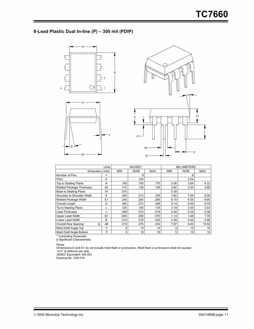
8-Lead Plastic Dual In-line (P) – 300 mil (PDIP)B1
B
A1
A
L
A2
p
α
E
eB
β
c
E1
n
D
1
2
Units INCHES* MILLIMETERSDimension Limits MIN NOM MAX MIN NOM MAX
Number of Pins n 8 8Pitch p .100 2.54Top to Seating Plane A .140 .155 .170 3.56 3.94 4.32Molded Package Thickness A2 .115 .130 .145 2.92 3.30 3.68Base to Seating Plane A1 .015 0.38Shoulder to Shoulder Width E .300 .313 .325 7.62 7.94 8.26Molded Package Width E1 .240 .250 .260 6.10 6.35 6.60Overall Length D .360 .373 .385 9.14 9.46 9.78Tip to Seating Plane L .125 .130 .135 3.18 3.30 3.43Lead Thickness c .008 .012 .015 0.20 0.29 0.38Upper Lead Width B1 .045 .058 .070 1.14 1.46 1.78Lower Lead Width B .014 .018 .022 0.36 0.46 0.56Overall Row Spacing § eB .310 .370 .430 7.87 9.40 10.92Mold Draft Angle Top α 5 10 15 5 10 15Mold Draft Angle Bottom β 5 10 15 5 10 15* Controlling Parameter
Notes:Dimensions D and E1 do not include mold flash or protrusions. Mold flash or protrusions shall not exceed
JEDEC Equivalent: MS-001Drawing No. C04-018
.010” (0.254mm) per side.
§ Significant Characteristic
2002 Microchip Technology Inc. DS21465B-page 11

TC7660
8-Lead Ceramic Dual In-line – 300 mil (CERDIP)Packaging diagram not available at this time.
DS21465B-page 12 2002 Microchip Technology Inc.

TC7660
8-Lead Plastic Small Outline (SN) – Narrow, 150 mil (SOIC)Foot Angle φ 0 4 8 0 4 8
1512015120βMold Draft Angle Bottom1512015120αMold Draft Angle Top
0.510.420.33.020.017.013BLead Width0.250.230.20.010.009.008cLead Thickness
0.760.620.48.030.025.019LFoot Length0.510.380.25.020.015.010hChamfer Distance5.004.904.80.197.193.189DOverall Length3.993.913.71.157.154.146E1Molded Package Width6.206.025.79.244.237.228EOverall Width0.250.180.10.010.007.004A1Standoff §1.551.421.32.061.056.052A2Molded Package Thickness1.751.551.35.069.061.053AOverall Height
1.27.050pPitch88nNumber of Pins
MAXNOMMINMAXNOMMINDimension LimitsMILLIMETERSINCHES*Units
2
1
D
n
p
B
E
E1
h
Lβ
c
45°
φ
A2
α
A
A1
* Controlling Parameter
Notes:Dimensions D and E1 do not include mold flash or protrusions. Mold flash or protrusions shall not exceed .010” (0.254mm) per side.JEDEC Equivalent: MS-012Drawing No. C04-057
§ Significant Characteristic
2002 Microchip Technology Inc. DS21465B-page 13

TC7660
NOTES:DS21465B-page 14 2002 Microchip Technology Inc.

TC7660
PRODUCT IDENTIFICATION SYSTEMTo order or obtain information, e.g., on pricing or delivery, refer to the factory or the listed sales office.Sales and SupportData SheetsProducts supported by a preliminary Data Sheet may have an errata sheet describing minor operational differences and recom-mended workarounds. To determine if an errata sheet exists for a particular device, please contact one of the following:
1. Your local Microchip sales office2. The Microchip Corporate Literature Center U.S. FAX: (480) 792-72773. The Microchip Worldwide Site (www.microchip.com)
Please specify which device, revision of silicon and Data Sheet (include Literature #) you are using.
New Customer Notification SystemRegister on our web site (www.microchip.com/cn) to receive the most current information on our products.
PART NO. X /XX
PackageTemperatureRange
Device
Device: TC7660: DC-to-DC Voltage Converter
Temperature Range: C = 0°C to +70°CE = -40°C to +85°CI = -25°C to +85°C (CERDIP only)M = -55°C to +125°C (CERDIP only)
Package: PA = Plastic DIP, (300 mil body), 8-leadJA = Ceramic DIP, (300 mil body), 8-leadOA = SOIC (Narrow), 8-leadOA713 = SOIC (Narrow), 8-lead (Tape and Reel)
Examples:a) TC7660COA: Commercial Temp., SOIC
package.b) TC7660COA713:Tape and Reel, Commercial
Temp., SOIC package.c) TC7660CPA: Commercial Temp., PDIP
package.d) TC7660EOA: Extended Temp., SOIC
package.e) TC7660EOA713:Tape and Reel, Extended
Temp., SOIC package.f) TC7660EPA: Extended Temp., PDIP
package.g) TC7660IJA: Industrial Temp., CERDIP
packageh) TC7660MJA: Military Temp., CERDIP
package.
2002 Microchip Technology Inc. DS21465B-page15

TC7660
NOTES:DS21465B-page 16 2002 Microchip Technology Inc.
Note the following details of the code protection feature on Microchip devices:• Microchip products meet the specification contained in their particular Microchip Data Sheet.
• Microchip believes that its family of products is one of the most secure families of its kind on the market today, when used in the intended manner and under normal conditions.
• There are dishonest and possibly illegal methods used to breach the code protection feature. All of these methods, to our knowl-edge, require using the Microchip products in a manner outside the operating specifications contained in Microchip's Data Sheets. Most likely, the person doing so is engaged in theft of intellectual property.
• Microchip is willing to work with the customer who is concerned about the integrity of their code.
• Neither Microchip nor any other semiconductor manufacturer can guarantee the security of their code. Code protection does not mean that we are guaranteeing the product as “unbreakable.”
Code protection is constantly evolving. We at Microchip are committed to continuously improving the code protection features of ourproducts.
Information contained in this publication regarding deviceapplications and the like is intended through suggestion onlyand may be superseded by updates. It is your responsibility toensure that your application meets with your specifications.No representation or warranty is given and no liability isassumed by Microchip Technology Incorporated with respectto the accuracy or use of such information, or infringement ofpatents or other intellectual property rights arising from suchuse or otherwise. Use of Microchip’s products as critical com-ponents in life support systems is not authorized except withexpress written approval by Microchip. No licenses are con-veyed, implicitly or otherwise, under any intellectual propertyrights.
2002 Microchip Technology Inc.
Trademarks
The Microchip name and logo, the Microchip logo, KEELOQ,MPLAB, PIC, PICmicro, PICSTART and PRO MATE areregistered trademarks of Microchip Technology Incorporatedin the U.S.A. and other countries.
FilterLab, microID, MXDEV, MXLAB, PICMASTER, SEEVALand The Embedded Control Solutions Company areregistered trademarks of Microchip Technology Incorporatedin the U.S.A.
dsPIC, dsPICDEM.net, ECONOMONITOR, FanSense,FlexROM, fuzzyLAB, In-Circuit Serial Programming, ICSP,ICEPIC, microPort, Migratable Memory, MPASM, MPLIB,MPLINK, MPSIM, PICC, PICDEM, PICDEM.net, rfPIC, SelectMode and Total Endurance are trademarks of MicrochipTechnology Incorporated in the U.S.A. and other countries.
Serialized Quick Turn Programming (SQTP) is a service markof Microchip Technology Incorporated in the U.S.A.
All other trademarks mentioned herein are property of theirrespective companies.
© 2002, Microchip Technology Incorporated, Printed in theU.S.A., All Rights Reserved.
Printed on recycled paper.
DS21465B - page 17
Microchip received QS-9000 quality system certification for its worldwide headquarters, design and wafer fabrication facilities in Chandler and Tempe, Arizona in July 1999 and Mountain View, California in March 2002. The Company’s quality system processes and procedures are QS-9000 compliant for its PICmicro® 8-bit MCUs, KEELOQ® code hopping devices, Serial EEPROMs, microperipherals, non-volatile memory and analog products. In addition, Microchip’s quality system for the design and manufacture of development systems is ISO 9001 certified.

DS21465B-page 18 2002 Microchip Technology Inc.
MAMERICASCorporate Office2355 West Chandler Blvd.Chandler, AZ 85224-6199Tel: 480-792-7200 Fax: 480-792-7277Technical Support: 480-792-7627Web Address: http://www.microchip.comRocky Mountain2355 West Chandler Blvd.Chandler, AZ 85224-6199Tel: 480-792-7966 Fax: 480-792-4338Atlanta3780 Mansell Road, Suite 130Alpharetta, GA 30022Tel: 770-640-0034 Fax: 770-640-0307Boston2 Lan Drive, Suite 120Westford, MA 01886Tel: 978-692-3848 Fax: 978-692-3821Chicago333 Pierce Road, Suite 180Itasca, IL 60143Tel: 630-285-0071 Fax: 630-285-0075Dallas4570 Westgrove Drive, Suite 160Addison, TX 75001Tel: 972-818-7423 Fax: 972-818-2924DetroitTri-Atria Office Building 32255 Northwestern Highway, Suite 190Farmington Hills, MI 48334Tel: 248-538-2250 Fax: 248-538-2260Kokomo2767 S. Albright Road Kokomo, Indiana 46902Tel: 765-864-8360 Fax: 765-864-8387Los Angeles18201 Von Karman, Suite 1090Irvine, CA 92612Tel: 949-263-1888 Fax: 949-263-1338San JoseMicrochip Technology Inc.2107 North First Street, Suite 590San Jose, CA 95131Tel: 408-436-7950 Fax: 408-436-7955Toronto6285 Northam Drive, Suite 108Mississauga, Ontario L4V 1X5, CanadaTel: 905-673-0699 Fax: 905-673-6509
ASIA/PACIFICAustraliaMicrochip Technology Australia Pty LtdSuite 22, 41 Rawson StreetEpping 2121, NSWAustraliaTel: 61-2-9868-6733 Fax: 61-2-9868-6755China - BeijingMicrochip Technology Consulting (Shanghai)Co., Ltd., Beijing Liaison OfficeUnit 915Bei Hai Wan Tai Bldg.No. 6 Chaoyangmen Beidajie Beijing, 100027, No. ChinaTel: 86-10-85282100 Fax: 86-10-85282104China - ChengduMicrochip Technology Consulting (Shanghai)Co., Ltd., Chengdu Liaison OfficeRm. 2401-2402, 24th Floor, Ming Xing Financial TowerNo. 88 TIDU StreetChengdu 610016, ChinaTel: 86-28-86766200 Fax: 86-28-86766599China - FuzhouMicrochip Technology Consulting (Shanghai)Co., Ltd., Fuzhou Liaison OfficeUnit 28F, World Trade PlazaNo. 71 Wusi RoadFuzhou 350001, ChinaTel: 86-591-7503506 Fax: 86-591-7503521China - ShanghaiMicrochip Technology Consulting (Shanghai)Co., Ltd.Room 701, Bldg. BFar East International PlazaNo. 317 Xian Xia RoadShanghai, 200051Tel: 86-21-6275-5700 Fax: 86-21-6275-5060China - ShenzhenMicrochip Technology Consulting (Shanghai)Co., Ltd., Shenzhen Liaison OfficeRm. 15-16, 13/F, Shenzhen Kerry Centre,Renminnan LuShenzhen 518001, ChinaTel: 86-755-82350361 Fax: 86-755-82366086China - Hong Kong SARMicrochip Technology Hongkong Ltd.Unit 901-6, Tower 2, Metroplaza223 Hing Fong RoadKwai Fong, N.T., Hong KongTel: 852-2401-1200 Fax: 852-2401-3431IndiaMicrochip Technology Inc.India Liaison OfficeDivyasree Chambers1 Floor, Wing A (A3/A4)No. 11, O’Shaugnessey RoadBangalore, 560 025, IndiaTel: 91-80-2290061 Fax: 91-80-2290062
JapanMicrochip Technology Japan K.K.Benex S-1 6F3-18-20, ShinyokohamaKohoku-Ku, Yokohama-shiKanagawa, 222-0033, JapanTel: 81-45-471- 6166 Fax: 81-45-471-6122KoreaMicrochip Technology Korea168-1, Youngbo Bldg. 3 FloorSamsung-Dong, Kangnam-KuSeoul, Korea 135-882Tel: 82-2-554-7200 Fax: 82-2-558-5934SingaporeMicrochip Technology Singapore Pte Ltd.200 Middle Road#07-02 Prime CentreSingapore, 188980Tel: 65-6334-8870 Fax: 65-6334-8850TaiwanMicrochip Technology (Barbados) Inc., Taiwan Branch11F-3, No. 207Tung Hua North RoadTaipei, 105, TaiwanTel: 886-2-2717-7175 Fax: 886-2-2545-0139
EUROPEAustriaMicrochip Technology Austria GmbHDurisolstrasse 2A-4600 WelsAustriaTel: 43-7242-2244-399Fax: 43-7242-2244-393DenmarkMicrochip Technology Nordic ApSRegus Business CentreLautrup hoj 1-3Ballerup DK-2750 DenmarkTel: 45 4420 9895 Fax: 45 4420 9910FranceMicrochip Technology SARLParc d’Activite du Moulin de Massy43 Rue du Saule TrapuBatiment A - ler Etage91300 Massy, FranceTel: 33-1-69-53-63-20 Fax: 33-1-69-30-90-79GermanyMicrochip Technology GmbHSteinheilstrasse 10D-85737 Ismaning, GermanyTel: 49-89-627-144 0 Fax: 49-89-627-144-44ItalyMicrochip Technology SRLCentro Direzionale Colleoni Palazzo Taurus 1 V. Le Colleoni 120041 Agrate BrianzaMilan, Italy Tel: 39-039-65791-1 Fax: 39-039-6899883United KingdomMicrochip Ltd.505 Eskdale RoadWinnersh TriangleWokingham Berkshire, England RG41 5TUTel: 44 118 921 5869 Fax: 44-118 921-5820
11/15/02
WORLDWIDE SALES AND SERVICE