Embed Size (px)
Citation preview

ChemicalScience
MINIREVIEW
Ope
n A
cces
s A
rtic
le. P
ublis
hed
on 2
4 Se
ptem
ber
2018
. Dow
nloa
ded
on 3
/26/
2022
1:3
8:42
PM
. T
his
artic
le is
lice
nsed
und
er a
Cre
ativ
e C
omm
ons
Attr
ibut
ion-
Non
Com
mer
cial
3.0
Unp
orte
d L
icen
ce.
View Article OnlineView Journal | View Issue
Charge carrier inj
JrTSMtPIeUdES
of King Abdullah University of Scienpast research activities include metatronic devices including transistorsMore recently, his research focuses ocarrier transport through 2D-TMD la
Computer, Electrical and Mathematical S
University of Science and Technology, T
Arabia. E-mail: [email protected]
Cite this: Chem. Sci., 2018, 9, 7727
All publication charges for this articlehave been paid for by the Royal Societyof Chemistry
Received 13th June 2018Accepted 23rd September 2018
DOI: 10.1039/c8sc02609b
rsc.li/chemical-science
This journal is © The Royal Society of C
ection and transport engineering intwo-dimensional transition metal dichalcogenides
Jose Ramon Duran Retamal, Dharmaraj Periyanagounder, Jr-Jian Ke,Meng-Lin Tsai and Jr-Hau He *
Ever since two dimensional-transition (2D) metal dichalcogenides (TMDs) were discovered, their fascinating
electronic properties have attracted a great deal of attention for harnessing them as critical components in
novel electronic devices. 2D-TMDs endowed with an atomically thin structure, dangling bond-free nature,
electrostatic integrity, and tunable wide band gaps enable low power consumption, low leakage, ambipolar
transport, high mobility, superconductivity, robustness against short channel effects and tunneling in highly
scaled devices. However, the progress of 2D-TMDs has been hampered by severe charge transport issues
arising from undesired phenomena occurring at the surfaces and interfaces. Therefore, this review provides
three distinct engineering strategies embodied with distinct innovative approaches to optimize both carrier
injection and transport. First, contact engineering involves 2D-metal contacts and tunneling interlayers to
overcome metal-induced interface states and the Fermi level pinning effect caused by low vacancy energy
formation. Second, dielectric engineering covers high-k dielectrics, ionic liquids or 2D-insulators to screen
scattering centers caused by carrier traps, imperfections and rough substrates, to finely tune the Fermi level
across the band gap, and to provide dangling bond-free media. Third, material engineering focuses on
charge transfer via substitutional, chemical and plasma doping to precisely modulate the carrier
concentration and to passivate defects while preserving material integrity. Finally, we provide an outlook of
the conceptual and technical achievements in 2D-TMDs to give a prospective view of the future
development of highly scaled nanoelectronic devices.
ose Ramon Duran Retamaleceived his B.S. (2007) from theelecommunication Engineeringchool, Technical University ofadrid, M.S. (2010) from Elec-
rical Engineering Department andh.D. (2014) from the Graduatenstitute of Photonics and Opto-lectronics at the National Taiwanniversity. Currently, he is a post-octoral fellow at the Computer,lectrical and Mathematicalciences and Engineering Divisionce and Technology (KAUST). Hisl oxide nanostructure based elec-, photodetectors, and memories.n elucidating and improving theteral heterojunctions.
ciences and Engineering, King Abdullah
huwal, 23955-6900, Kingdom of Saudi
hemistry 2018
1. Introduction
SinceMoore's law was proposed in 1965 and with the advance ofconventional Si technology, the semiconductor industry has
Dharmaraj Periyanagounder isworking as a visiting student inthe Electrical EngineeringDepartment at the Computer,Electrical and MathematicalSciences and Engineering(CEMSE) Division of the KingAbdullah University of Scienceand Technology (KAUST).Dharma's research interests arethe device physics of 2D mate-rials and their heterostructuresfor technologically useful elec-
tronic, optoelectronic and thermoelectric applications. He is nowextensively involved in the micro/nanofabrication of 2D material-based devices by high resolution e-beam lithography.
Chem. Sci., 2018, 9, 7727–7745 | 7727

Chemical Science Minireview
Ope
n A
cces
s A
rtic
le. P
ublis
hed
on 2
4 Se
ptem
ber
2018
. Dow
nloa
ded
on 3
/26/
2022
1:3
8:42
PM
. T
his
artic
le is
lice
nsed
und
er a
Cre
ativ
e C
omm
ons
Attr
ibut
ion-
Non
Com
mer
cial
3.0
Unp
orte
d L
icen
ce.
View Article Online
been consistently and prosperously developed over the pasthalf-century. However, as Si technology is approaching thefundamental size scaling limit in the sub 10 nm regime, thematerial roughness and the short channel effects (SCEs)dominate the carrier transport, which could infer the end ofMoore's law. Moreover, it is crucial to reduce the powerconsumption without sacricing device performance.1,2 Indeed,there exists a theoretical Boltzmann limit for subthresholdswing (SS, the gure-of-merit that determines the switchingcharacteristics of FETs) of 60 mV dec�1 at 300 K that can beovercome by tunneling transistors and negative capacitancetransistors.3–6 Therefore, the major challenge of the semi-conductor industry in the following years is to nd novel sub-nanometer materials and transistor geometries that enablehigh performance and low power consumption devices. Towardthis challenge, the superior electronic properties including theexcellent electrostatic integrity, tunable bandgaps, highelectron/hole mobility, and gate-tunable superconductivity ofnovel two dimensional-transition metal dichalcogenides (2D-TMDs) have enabled the development of nanoscale devices
Jr-Jian Ke received his B.S. (2007)in electrical engineering from theNational University of Kaoh-siung, Kaohsiung, Taiwan, andhis M.S. (2009) and Ph. D (2016)degrees from the Graduate Insti-tute of Photonics and Optoelec-tronics, National TaiwanUniversity, Taipei, Taiwan. Hispast research activities includethe transport mechanism ofnanowires and metal–semi-conductor interfaces. He is now
working on the fabrication and transport modeling of resistiverandom-access memory devices and their applications.
Meng-Lin Tsai received his B.S.degree from National Tsing HuaUniversity, Hsinchu, Taiwan. Heis currently with the Departmentof Electrical Engineering, andthe Graduate Institute ofPhotonics and Optoelectronics,National Taiwan University,Taipei, Taiwan. Currently, he isworking at Taiwan Semi-conductor ManufacturingCompany (TSMC).
7728 | Chem. Sci., 2018, 9, 7727–7745
with exceptional transport properties, thus holding promise forthe next-generation of semiconductor materials towards theirapplicability in diverse applications such as transistors, digitalcircuits, optoelectronic systems and chemical sensors.7–15 Ascharge carriers are strongly conned in atomically thin layers,the critical issues associated with SCEs can be completelyeliminated, thereby broadening the range of applicationstoward highly energy efficient devices.12,16,17 Furthermore, thegate controllable atomically thin TMD channel enables a highelectric eld at the tunnel junction to strongly increase the on-current and to reduce the subthermionic SS down to 3.9 mVdec�1, which provides a signicant breakthrough for applica-tions in the future semiconductor industry.18,19
Despite the growing interest in 2D-TMD materials, there areseveral bottlenecks that block the progress as well as the inte-gration of TMDs with modern semiconductor technology.20–22
Specically, and as prescribed by the international technologyroadmap for semiconductors (ITRS), the primary step towardhighly efficient electronic devices is that the metal electrode/TMD contact resistance (RC) should be as low as �100 U mm.23
This is not the case for most 2D-TMD based devices fabricatedso far due to their detrimental interface states.22,24 In addition,owing to the nature of the metal/TMD chemical bond, thecontact geometry plays a key role in determining RC. On theother hand, the carrier transport efficiency, mainly limited bycarrier traps and phonon-scattering centers, can be notoriouslyaffected by impurities or imperfections along the channel owingto the high surface-to-volume ratio of 2D-TMDs, hencebecoming a cornerstone toward high mobility devices.25–31 Inthis regard, strategies engineering the surrounding gatedielectric as well as functionalizing the surface play a starringrole in boosting the performance.20,32 Consequently, it is ofparamount importance to deeply scrutinize not only thefundamental limitations of the current transport but also thestrategies to overcome such limitations in order to preciselycontrol the electronic properties of 2D-TMDs toward high
Dr. Jr-Hau He is an AssociateProfessor of Electrical Engi-neering program at King Abdul-lah University of Science &Technology (KAUST). His break-through research in 2Dmaterials/electronics and pho-toelectrochemical water split-ting has been highlighted over50 times by various scienticmagazines such as Nature,Nature Materials, IEEE SPEC-TRUM, EE Times, Semi-
conductor Today, Materials Today, Chemical & Engineering News,and Nano Today. He participates actively in activities and servicesin scientic professional societies. He is a Fellow of RSC and SPIE,and a senior member of IEEE and OSA.
This journal is © The Royal Society of Chemistry 2018
Minireview Chemical Science
Ope
n A
cces
s A
rtic
le. P
ublis
hed
on 2
4 Se
ptem
ber
2018
. Dow
nloa
ded
on 3
/26/
2022
1:3
8:42
PM
. T
his
artic
le is
lice
nsed
und
er a
Cre
ativ
e C
omm
ons
Attr
ibut
ion-
Non
Com
mer
cial
3.0
Unp
orte
d L
icen
ce.
View Article Online
performance electronic devices beyond scaling and physicallimits.
Accordingly, we summarize recent advances and challengesencountered in the development of 2D-TMD based electronicdevices. First, we provide insight on factors inuencing thecarrier injection such as the Fermi level pinning (FLP) or theSchottky barrier (SB), and accordingly how to precisely estimateRC. Second, based on the scattering limited mobility edgeconcept, we discern the current transport mechanism along thechannel and emphasize the carrier-density-dependent metal-to-insulator (MIT) transition as well as the ballistic transport ofhighly scaled devices. Third, we review how several strategiesinvolving surface and interface chemistry can synergisticallyimprove both carrier injection and current transport, high-lighting the importance of doping and phase transformation.Finally, we provide an outlook of the major achievements andgive a perspective of future research directions for developinghigh performance 2D-TMD based electronic devices.
2. Contact resistance and currenttransport in 2D-TMDs
To discuss the electronic properties of 2D-TMDs, we rstdiscuss the theoretical framework, current transport mecha-nism and experimental accuracy to understand how the proc-essability, low dimensionality and novel properties of 2D-TMDslimit the carrier injection due to high contact resistance and
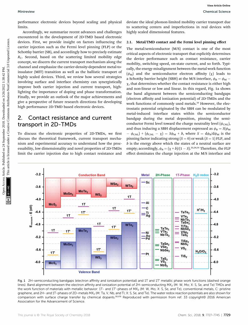
Fig. 1 2H-semiconducting bandgaps (electron affinity and ionization polines). Band alignment between the electron affinity and ionization potenthe work function of materials with metallic behavior: 1T- and 1T0-phasegraphene, and 2H- and 1T-phases of 2D-metals MX2 (M: Ta, V, Nb, and Ti;comparison with surface charge transfer by chemical dopants.33,172 ReAssociation for the Advancement of Science.
This journal is © The Royal Society of Chemistry 2018
deviate the ideal phonon-limited mobility carrier transport dueto scattering centers and imperfections in real devices withhighly scaled dimensional features.
2.1. Metal/TMD contact and the Fermi level pinning effect
The metal/semiconductor (M/S) contact is one of the mostcritical aspects of electronic transport that explicitly determinesthe device performance such as contact resistance, carriermobility, switching speed, on-state current, and so forth. Typi-cally, the energy misalignment between themetal work function(fM) and the semiconductor electron affinity (c) leads toa Schottky barrier height (SBH) at the M/S interface, fB ¼ fM �c, that determines whether the contact resistance is either highand non-linear or low and linear. In this regard, Fig. 1a showsthe band alignment between the semiconducting bandgaps(electron affinity and ionization potential) of 2D-TMDs and thework functions of commonly used metals.33 However, the elec-trostatic potential originated by the SBH can be modulated bymetal-induced interface states within the semiconductorbandgap during the metal deposition, pinning the semi-conductor Fermi level toward the charge neutrality level (fCNL),and thus inducing a SBH displacement expressed as fB ¼ S(fM
� fCNL) + (fCNL � c) ¼ SfM + b, where S ¼ dfB/dfM is thepinning factor indicating strong (S¼ 0) or weak (S¼ 1) FLP, andb is the energy above which the states of a neutral surface areempty; accordingly, fB ¼ (c + b)/(1� S).22,24,31 Therefore, the FLPeffect dominates the charge injection at the M/S interface and
tential) and 1T and 1T0 metallic phase work functions (dashed orangetial of 2H-semiconducting MX2 (M: W, Mo; X: S, Se, and Te) TMDs ands of MX2 (M: W, Mo; X: S, Se, and Te), conventional metals, C: pristineX: S, Se, and Te). Thewater redox reaction potentials are also shown forproduced with permission from ref. 33 copyright© 2016 American
Chem. Sci., 2018, 9, 7727–7745 | 7729
Chemical Science Minireview
Ope
n A
cces
s A
rtic
le. P
ublis
hed
on 2
4 Se
ptem
ber
2018
. Dow
nloa
ded
on 3
/26/
2022
1:3
8:42
PM
. T
his
artic
le is
lice
nsed
und
er a
Cre
ativ
e C
omm
ons
Attr
ibut
ion-
Non
Com
mer
cial
3.0
Unp
orte
d L
icen
ce.
View Article Online
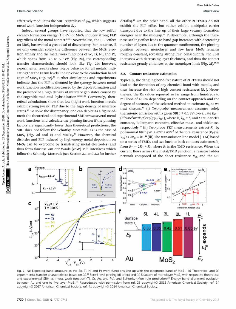
effectively modulates the SBH regardless of fM, which suggestsmetal work function independent RC.
Indeed, several groups have reported that the low sulfurvacancy formation energy (1.6 eV) of MoS2 induces strong FLPregardless of the metal contact.24,34 Nevertheless, the FLP effecton MoS2 has evoked a great deal of discrepancy. For instance, ifwe only consider solely the difference between the MoS2 elec-tron affinity and the metal work functions of Sc, Ti, Ni, and Pt,which spans from 3.5 to 5.9 eV (Fig. 2a), the correspondingtransfer characteristics should look like Fig. 2b; however,experimental results show n-type behavior for all metals, indi-cating that the Fermi levels line-up close to the conduction bandedge of MoS2 (Fig. 2c).23 Further simulations and experimentsindicate that the FLP is dictated by the synergy between metalwork function modication caused by the dipole formation andthe presence of a high density of interface gap states caused bychalcogenide-mediated hybridization.23,35–38 Conversely, theo-retical calculations show that low (high) work function metalsexhibit strong (weak) FLP due to the high density of interfacestates.39 To solve the discrepancy, one can depict as a gure-of-merit the theoretical and experimental SBH versus several metalwork functions and calculate the pinning factor; if the pinningfactors are signicantly lower than theoretical predictions, theSBH does not follow the Schottky–Mott rule, as is the case ofMoS2 (Fig. 2d and e) and MoTe2.24 However, the chemicaldisorder and FLP induced by high-energy metal deposition onMoS2 can be overcome by transferring metal electrodes, andthus form awless van der Waals (vdW) M/S interfaces whichfollow the Schottky–Mott rule (see Section 3.1 and 3.2 for further
Fig. 2 (a) Expected band structure as the Sc, Ti, Ni and Pt work functiexperimental transfer characteristics based on (a).23 Fermi level pinning (dand experimental SBH vs. metal work function (Ti, Cr, Au, and Pd), anbetween Au and one to five layer MoS2.41 Reproduced with permissiocopyright© 2017 American Chemical Society; ref. 41 copyright© 2014 A
7730 | Chem. Sci., 2018, 9, 7727–7745
details).40 On the other hand, all the other 2D-TMDs do notexhibit the FLP effect but rather exhibit ambipolar carriertransport due to the line up of their large vacancy formationenergies near the mid-gap.34 Furthermore, although the thick-ness scaling effect leads to band gap increases with decreasingnumber of layers due to the quantum connement, the pinningposition between monolayer and few layer MoS2 remainsroughly constant, revealing strong FLP; consequently, the SBHincreases with decreasing layer thickness, and thus the contactresistance greatly enhances at the monolayer limit (Fig. 2f).10,41
2.2. Contact resistance estimation
Typically, the dangling bond-free nature of 2D-TMDs should notlead to the formation of any chemical bond with metals, andthus increase the risk of high contact resistances (RC). Never-theless, the RC values reported so far range from hundreds tomillions of U mm depending on the contact approach and thedegree of accuracy of the selected method to estimate RC as wenext discuss.42 (i) Two-probe measurement assumes solelythermionic emission with a given SBH# 0.1 eV to evaluate RC ¼(h3/4pe2m*tkBT)exp(qfB/kBT), where h, kB,m*, and t are Planck'sconstant, Boltzmann constant, effective mass, and thickness,respectively.43 (ii) Two-probe FET measurements extract RC bypolynomial tting b1 + b2/x + b3/x2 of the total resistance (RT) vs.Vgs as 2RC ¼ b1.44 (iii) The transmission line model (TLM) basedon a series of TMDs and two back-to-back contacts estimates RC
from RT ¼ 2RC + Ri, where Ri is the TMD resistance. When thecurrent ows across the metal/TMD junction, a resistor laddernetwork composed of the sheet resistance Rsh and the SB-
ons line up with the electronic band of MoS2. (b) Theoretical and (c)) effect and (e) S factors of monolayer MoS2 with respect to theoreticald Schottky–Mott rule prediction.24 Energy band alignment evolutionn from ref. 23 copyright© 2013 American Chemical Society; ref. 24merican Chemical Society.
This journal is © The Royal Society of Chemistry 2018

Minireview Chemical Science
Ope
n A
cces
s A
rtic
le. P
ublis
hed
on 2
4 Se
ptem
ber
2018
. Dow
nloa
ded
on 3
/26/
2022
1:3
8:42
PM
. T
his
artic
le is
lice
nsed
und
er a
Cre
ativ
e C
omm
ons
Attr
ibut
ion-
Non
Com
mer
cial
3.0
Unp
orte
d L
icen
ce.
View Article Online
induced specic contact resistivity rc leads to RC ¼ (RshLT/W)
coth(L/LT), where L is the contact length and LT ¼ ffiffiffiffiffiffiffiffiffiffiffiffiffiffirC=Rsh
pis
the effective contact transfer length for the carrier injection,a parameter that describes the distance over which 1/e of thecurrent is transferred to the metal contact (Fig. 3).45–47 For shortLT, the current crosses around the contact edge, while for longLT, the current involves larger contact areas.45 This currentinjection phenomenon, termed as current crowding, imposesdevice scaling limits because if L < LT, RC increases abruptly.48,49
Therefore, keeping L[ 1.5 LT is crucial to avoid high RC and tokeep L-independent RC when downscaling devices; conse-quently, coth(L/LT)� 1, and thus RC ¼ RshLT/W and RT ¼ Rsh(2LT+ Lch)/W, where Lch is the channel length. The linear t of RT vs.Lch plot allows the extraction of 2RC, 2LT and Rsh from theintersection with the RT axis, Lch axis and the slope, respectively.(iv) Four-probe measurements lead to RC ¼ (V2p/Isd � (V4p/Isd) �(L2p/L4p)) � W, where W is the channel width and Isd, V2p (V4p),and L2p (L4p) are the source-drain (probing contacts) current,voltage drops and length, respectively.50 (v) Four-probe FETmeasurement avoids the potential drop in the sensing probes,and thus RC can be extracted independently for each lead.42 (vi)The Y-function method is more realistic since it allows theextraction of RC from the FET linear region while consideringphonon and surface scattering events as well as the voltage dropinduced by the SB.51
2.3. Carrier injection at the metal/TMD contact
In the presence of a moderate SB, the main transport mecha-nism across the metal/TMD interface is thermionic emission,which can be described as
I ¼ I2D exp(qV/hkBT)[1 � exp(�qV/kBT)] (1)
I2D ¼ WA*2DT
3=2 exp
�� qfB
kBT
�; (2)
Fig. 3 Schematic view of current flow across metal/TMD junctions.
This journal is © The Royal Society of Chemistry 2018
where I2D is the saturation current,W is the junction length, q isthe electron charge, fB is the SBH, h is the ideality factor, V is
the voltage bias, and A*2D ¼ qffiffiffiffiffiffiffiffiffiffiffiffiffiffiffiffiffiffiffi8pkB3m*
p=h2 is the 2D equivalent
Richardson constant with m* being the electron effective mass(Table 1).24,49,52–54 It is also noteworthy that TMDs exhibit layerdependent effective mass, for instance the effective mass ofMoS2 varies from 0.41m0 to 0.57m0 from monolayer to few-layer.55 At sufficient forward bias, the image charge-inducedbarrier lowering accounted for by the ideality factor can beextrapolated from q/2.3hkBT ¼ slope of the linear tting ofthe semilog I vs. V or log[I/(1 � exp(�qV/kBT))] vs. V plots.54
Meanwhile, at sufficient reverse bias (qV [ kBT)
IzWA*2DT3=2 expð�qfB=kBTÞ; therefore, SBH can be calculated
from current–temperature measurements as fB ¼ (kB/q)(Dln(I/T3/2)/DT�1) (Fig. 4a–c).24,35 However, the veracity of the as-extracted SBH should be revised when fB < 3kBT or fB <0 because such a SBH is not effective for carrier blocking.31,56,57
Beyond thermionic emission, the applied bias conguration,doping level and temperature can enable direct tunneling (DT;eld emission) through a wide-trapezoidal barrier at the quasi-Fermi level and/or thermally assisted Fowler–Nordheimtunneling (FNT; thermionic eld emission) through a thin-triangular barrier above the Fermi level but below the top ofthe SB.58 To discern whether DT or FNT dominates, the ln(I/V2)vs. (I/V) plots should be explored as follows
IDT ¼ Aeffq2V
ffiffiffiffiffiffiffiffiffiffiffiffiffiffi2m*fB
ph2d
exp
�4pd ffiffiffiffiffiffiffiffiffiffiffiffiffiffi
2m*fB
ph
!(3)
ln
�IDT
V 2
�fln
�1
V
�� 4pd
ffiffiffiffiffiffiffiffiffiffiffiffiffiffi2m*fB
ph
(4)
IFNT ¼ Aeffq3m0V
2
8phfBd2m*
exp
0@�8pd
ffiffiffiffiffiffiffiffiffiffiffiffiffiffiffiffi2m*fB
3p3hqV
1A (5)
ln
�IFNT
V 2
�f� 1
V
0@8pd
ffiffiffiffiffiffiffiffiffiffiffiffiffiffiffiffi2m*fB
3p3hq
1A; (6)
where d is the SB width.59 Accordingly, the SBH can be evaluatedby inspecting if the FNT (DT) shows a linear (exponential) trend
Table 1 Direct band gap (Eg [eV]), electron effective mass ðm*e½m0�Þ,
dielectric constant (3 [30]), natural scaling length (l [nm]) for 2 nm thickHfO2 (3ox¼ 25), subthreshold slope (SS [mV dec�1]), and drain-inducedbarrier lowering (DIBL [mV V�1]) of monolayer TMDs.94,95 Reproducedwith permission from ref. 94 © 2013, IEEE; ref. 95 © 2014, AppliedPhysics Letters
TMD Eg [eV] m*e½m0� 3 [30] l [nm]
SS[mV dec�1]
DIBL[mV V�1]
MoS2 1.8 0.56 4.8 0.41 �60 �10MoSe2 1.51 0.62 6.9 0.49 �65 �15MoTe2 1.10 0.64 8.0 0.54 �70 �20WS2 1.93 0.33 4.4 0.40 �60 �7WSe2 1.62 0.35 4.5 0.42 �63 �10
Chem. Sci., 2018, 9, 7727–7745 | 7731

Fig. 4 SBH derivation of Co-contacted monolayer MoS2 from (a) the I–V curve, (b) the Arrhenius plot, and (c) the slope (S) extracted from theArrhenius plot.35 SBH derivation of Ni-contacted 3 nm MoS2 from (d) the transfer characteristics, (e) the Arrhenius plot, and (c) the extractedeffective SBH as a function of the gate voltage.23 SBH derivation of graphene-contacted WSe2 from (g) the I–V curve, (h) the temperaturedependent If–Vf plot, and (i) the slope extracted from the Is vs. 1/F00 plot.64 Reproduced with permission from ref. 35 © 2013, American ChemicalSociety; ref. 23 © 2012, American Chemical Society; ref. 64 © 2014, American Chemical Society.
Chemical Science Minireview
Ope
n A
cces
s A
rtic
le. P
ublis
hed
on 2
4 Se
ptem
ber
2018
. Dow
nloa
ded
on 3
/26/
2022
1:3
8:42
PM
. T
his
artic
le is
lice
nsed
und
er a
Cre
ativ
e C
omm
ons
Attr
ibut
ion-
Non
Com
mer
cial
3.0
Unp
orte
d L
icen
ce.
View Article Online
in the ln(I/V2) vs. (1/V) plot.59,60 In fact, several groups havecombined tunneling transport and FLP at the mid-gap toelucidate both the truly SBH, that is the at band potential (VFB),and the ambipolar behavior.22–24,50,58,61–63 The method assumesthermally activated conduction through the channel as long asVgs < VFB, that is why the activation energy is linear with Vgs.35,61
Thereby, the linear slope of semilog Ids vs. 1/T plots elucidatesthe equivalent SB ðf*
BÞ at different gate bias, and thus VFB can berealized by nding at which Vgs the f*
B vs. Vgs deviates fromlinearity (Fig. 4d–f). Alternatively, the thermally assistedtunneling transport can be described as I¼ Isexp(qV/F00), whereIs is the saturation current at zero forward voltage and F00 is thecharacteristic energy, both being related as Is f exp(fB/F00).Accordingly, Is and F00 can be extracted from the linear t ofln(I) vs. V at different temperatures, and fB can be extracted bythe semi-logarithmic slope of Is vs. 1/F00 (Fig. 4g–i).35,64
2.4. Carrier mobility and carrier scattering effects
To investigate the intrinsic charge transport properties ofTMDs, it is of paramount importance to properly assess theeffective carrier mobility of high quality samples only limited byphonon scattering events. Precise mobility assessment can bedone by Hall measurements, the Y-function method, and four-probe or two-probe based transconductance measurements but
7732 | Chem. Sci., 2018, 9, 7727–7745
without RC effects as follows, mFE ¼ (LCg/W)(v(1/(RT � 2RC))/vVgs), where L and W are the channel length and width,respectively.51,65–67 Nevertheless, the presence of Coulombimpurities at the TMD/dielectric interface and defects in lowquality samples as well as the substrate roughness affect noto-riously the mobility.30 According to Matthiessen's rule, theoverall scattered-limited mobility becomes m(n,T)�1 ¼mCoulomb(n,T)
�1 + mph(T)�1 + m�1
sr where mCoulomb, mph and msr arethe Coulomb scattering, phonon scattering, and surfaceroughness phonon scattering, respectively.20,25,68 At lowtemperatures, the mobility is mostly limited by Coulomb scat-tering arising from ionized impurity charges xed at the bottomsubstrate.69 Moreover, the Coulomb scattering is highly inten-sied in monolayer TMDs due to the short-interaction distancebetween impurities and carriers. Indeed, an increasing numberof layers lead to a higher dielectric constant and charge redis-tribution far from the interface; as a result, the outer layerexperiences reduced Coulomb scattering leading to mobilitypeaking at �10–15 layers.20,25,29,68,70–74 In this regard, experi-mental results have evidenced Hall mobilities up to 1000(34 000) cm2 V�1 s�1 for 1L (6L) MoS2 at 5 K.25,26,75 At highertemperatures, the electron–phonon interaction becomesdominant, leading to phonon-limited carrier mobility.76,77 Thephonon scattering temperature dependence follows the power
This journal is © The Royal Society of Chemistry 2018

Fig. 5 (a) Mobility edge concept for carrier transport via hopping(thermal activation) at deep (shallow) localized states or band transportat extended edge states. (b) Carrier distribution in 1, 5, and 14 layerchannels.29 Inset: illustration of equipotential electric field lines alongthe channel.90 Reproduced with permission from ref. 29 and 90 ©2013, American Chemical Society.
Minireview Chemical Science
Ope
n A
cces
s A
rtic
le. P
ublis
hed
on 2
4 Se
ptem
ber
2018
. Dow
nloa
ded
on 3
/26/
2022
1:3
8:42
PM
. T
his
artic
le is
lice
nsed
und
er a
Cre
ativ
e C
omm
ons
Attr
ibut
ion-
Non
Com
mer
cial
3.0
Unp
orte
d L
icen
ce.
View Article Online
law mph f T�g with g ranging from 0.55 to 1.7 for MoS2 (ref. 27,75 and 78) and 0.73 to 1.75 for WS2.79 The upper bond mobilitylimit is determined by the large effective mass and out-of-planepolar phonons (i.e. 410 cm2 V�1 s�1 for 1L MoS2).30,80 Never-theless, the highest mobilities reported to date at roomtemperature are 190 (700) cm2 V�1 s�1 for monolayer (10 nm)MoS2,23,81 and �250 cm2 V�1 s�1 for monolayer WSe2.82 On theother hand, atomically at TMDs exhibit negligible surfacescattering, in contrast to the severe surface scattering exhibitedby 5 nm rough ultrathin Si.30
2.5. Carrier transport and the scattering limited mobility-edge concept
To this extent, the mobility-edge concept, a boundary in theband tail that discriminates between extended and localizedstates, establishes a useful tool to assess the transport mecha-nism.28 Extended states enable metallic band-like transportcharacterized by decreasing mobility with increasing tempera-ture, whereas deep (local) localized states elucidate insulatingvariable range hopping (thermally activated) transport charac-terized by increasing mobility with increasing temperature(Fig. 5a). As the gate bias continuously modulates the Fermienergy from localized states to extended states, a metal-to-insulator transition (MIT) can be observed at the thresholdcarrier concentration.27,83 Below a certain carrier-density limit,the Fermi level lies on deep localized states caused by short-range disorder, leading to electrons owing by phononlimited thermally activated nearest-neighbor hopping (NNH)conduction at high temperature,84 where kBT1 is the energyspacing between the nearest neighbors, or by weak temperaturedependent variable-range hopping (VRH) conduction at lowtemperature, where T0 is the correlation energy, and d is thematerial dimensionality (d ¼ 2 for 2D-TMDs).70–72,85–87 However,as the Fermi level moves toward the conduction band localizedstates are lled and when the Fermi level enters the band-tailcarriers become mobile, enabling band-like conduction.71
Alternatively, thermally activated carriers from shallow local-ized states to the conduction band enable band-like conduc-tion, where Ea is the activation energy.27
2.6. Short channel effects and ballistic transport
Typically, the carrier concentration of bulk semiconductorscannot be fully tuned by gate bias because the electric potentialis not uniform across the thick bulk semiconductor. In contrast,the dangling-bond free nature and ultrathin structure of 2D-TMDs lead to highly conned carrier distribution close to thegate dielectric and highly uniform potential distribution alongthe channel, thus allowing homogeneous gating (Fig. 5b).29
Consequently, the drain–source electric eld lines fall mostly onthe surrounding environment, and thus the semiconductordepletion depth can be replaced by the TMD thickness (tbody)and the semiconductor dielectric constant can be regarded asthe environment (Fig. 5b).88–90 The electrostatic integrity can beevaluated by the drain-induced barrier lowering, where lowdrain-induced barrier lowering (DIBL) yields robustness againstshort channel effects (SCE).18,28,43,88 Indeed, to suppress SCEs
This journal is © The Royal Society of Chemistry 2018
and hence preserve the long channel behavior, the channellength should be at least 4–5 times longer than the electrostaticnatural scaling screening length, a gure of merit to distinguishbetween short and long channel behaviors, where tox and 3ox arethe thickness and dielectric constant of the gate oxide.28,58,73,88,91
Therefore, the rather low screening length enables gate tuningof the carrier concentration n ¼ Cg(Vg � Vth � Vds)/q, where thegate capacitance Cg should include the oxide capacitance (Cox),the TMD quantum capacitance (Cq), and the interface trapdensity capacitance, where Dit is the trap density.18,28,32,89,92
Nonetheless, in a double-gated geometry Cg should includeboth top and bottom gate capacitances.25,31,42,65,66,73 Further-more, as the channel length is scaled down to the electronmeanfree path, electronic devices are pushed from the diffusion limitto the scattering-free ballistic limit, at which the quantumconductance can potentially reach 2e2/h and the quantumcontact resistance can reach 30 U mm at a n2D of 1013 cm�2.22,93
To gain further insight on the SCE and ballistic transportcharacteristics of TMDs, Table 1 shows the l, SS and DIBLcalculated from ballistic transport simulations of scattering-free
Chem. Sci., 2018, 9, 7727–7745 | 7733
Chemical Science Minireview
Ope
n A
cces
s A
rtic
le. P
ublis
hed
on 2
4 Se
ptem
ber
2018
. Dow
nloa
ded
on 3
/26/
2022
1:3
8:42
PM
. T
his
artic
le is
lice
nsed
und
er a
Cre
ativ
e C
omm
ons
Attr
ibut
ion-
Non
Com
mer
cial
3.0
Unp
orte
d L
icen
ce.
View Article Online
15 nm short channels of monolayer TMDs with 2 nm thick HfO2
(3ox ¼ 25).94,95 The extremely low l < 0.5 nm causes a highlyintensied electric eld at TMD/contact junctions, enabling thepossibility to devise tunnel transistors with a high on-current of�500 mA mm�1 by engineering the TMD bandgap and effectivemass.95 In addition, negative differential resistance (NDR) canbe found along ballistic transport due to the narrow energydispersion of the TMD bands and the reduction of availablestates in the drain.94,96 Meanwhile, the SS of �60 mV dec�1 andDIBL of �10 mV V�1 suggest that at the monolayer limit thedielectric environment still dominates the vertical electric eldregardless of the TMD dielectric constant.43,94,97 Among theTMDs, the lower electron effective mass and dielectric constantof MoS2, WS2 and WSe2 than those of MoSe2 and MoTe2 lead tothe lowest SS and DIBL due to the diminished inuence of thedrain-triggered lateral electric eld.94 Accordingly, the largebandgap and relatively high effective mass of monolayer MoS2offer a signicant on–off ratio, 52% lower DIBL and 13% lowerSS than 3 nm Si at 10 nm channel length, and can lead to theDIBL of 100 mV V�1 of ITRS at 8 nm compared to 10 nm Si;97
nevertheless, the lower mobility than most III–V materialsmakes MoS2 more suited for low standby and operating powerthan high performance FETs.43 Furthermore, highly scaled p-WSe2 can meet the on-current ITRS requirements for high-performance p-FETs.98 However, monolayer TMDs still offerrelatively lower performance than hydrogenated silicene (i.e.silicane).98 On the other hand, the shortest channels experi-mentally fabricated so far are 10 nm-MoS2/graphene and 7.5 nm2H/1T MoS2 trenches, which have revealed a SS of 90–120 mVdec�1, an off-current of 10 pA mm�1, and an on–off ratio of 106–107.91,99 Alternatively, ultrashort effective channel lengthsdeveloped by top-gated FETs with 10 nm width air-oxidized Alstripes lead to a SS of 80 mV dec�1 with a high on-current of 400mA mm�1,100 whereas 1 nm carbon nanotube metal gates haveled to a SS of 65 mV dec�1 and an on–off ratio of 106.101 BesidesMoS2, dual gated BN-encapsulated and graphene-contactedWSe2 with 100 nm local gates has enabled Klein tunneling ofDirac fermions at 20 mK, resembling Fabry–Perot oscillationsand thus suggesting ballistic transport at the local gate.102
3. Carrier injection and carriertransport engineering strategies
We next discuss several engineering strategies to overcome theaforementioned carrier injection and carrier transport limita-tions toward improving the electronic properties of TMDs. Thestrategies can be divided roughly into three engineering cate-gories: contact, dielectric and material (Fig. 6a). As low RC iscompulsory for efficient carrier transport, we rst focus on thecontact geometry and how metals and interlayers can furtherimprove RC and different transport aspects. Second, we focus onhow surface defects and adsorbates affect the intrinsic elec-tronic properties of the conducting channel, and how thesurrounding dielectric passivates scattering centers and tunethe electronic transport. Third, we present distinct dopingtechniques, plasma treatments and phase transformation
7734 | Chem. Sci., 2018, 9, 7727–7745
approaches to tailor the electronic properties of TMDs. To graspthe great throughput of these strategies, Fig. 6b highlights themost remarkable achievements obtained by specic strategiesthat we detail in the next subsections.
3.1. Contact geometry engineering
The metal/TMD contact geometry either face-contact or edge-contact also plays a key role in the contact properties.22,37 Inthe face-contact mode, the direct metal deposition onto TMDfractures covalent bonds and originates defects, enhancing RC
due to FLP and high SB. However, transferred metals on 2D-TMDs circumvent the FLP, leading to well-controlled SBs bythe Schottky–Mott rule.40 Alternatively, conductive 2D-metalswith a wide range of work functions (Fig. 1) offer the possi-bility to eliminate metal-induced gap states and unbrokencovalent bonds by vertically stacking them on 2D-TMDs via vdWforces, thus reducing FLP and enabling tunable SB for bothelectrons and holes (Fig. 7a–c). For example, thermally stabledegenerate Nb0.005W0.995Se2/WSe2 contacts offer an extremelylow RC of 300 U mm, a world record on–off ratio of 109, anon-current of 320 mA mm�1 and mobilities of 200 and2000 cm2 V�1 s�2 at 300 K and 5 K respectively.103 Similarly, 2Dmetallic NbSe2/WSe2 elucidates ohmic contacts from directtunneling through lowered SB (Fig. 1).104 More interestingly,graphene as a face-contact material can reduce RC dynamicallyby pumping charge via band alignment modulation.105 On theother hand, edge-contact devised by atomically sharp interfacesstrongly reduces the FLP and enables control over the SB.106 Torealize edge-contact, several techniques have been formulatedas follows (Fig. 7d–f). (i) BN-sandwiched TMDs provide 1Datomic edge ohmic contacts with superior mobility andstability.26,50 (ii) Aromatic molecule-assisted in-planeatomic stitching enables large-scale graphene/MoS2 with a RC
of 300 U mm.107 (iii) Epitaxial growth of lateral graphene/MoS2,graphene/WSe2 and graphene/WS2 heterostructures results inRC as low as 11 kU mm, 50 kU mm and 30 kU mm, respec-tively.108–110 (iv) Degenerate edge contacts by alloying (i.e.WxNb1�xSe2/WSe2) or chemical doping (i.e. NO2-doped p+ WSe2,K-doped n+ WSe2, and P-doped p+-MoS2) lead to low interface-trap density ohmic contacts.82,111–113 (v) 2D-TMD lateral hetero-junctions.114,115 (vi) Phase transformation yields low SB due tothe close band alignment between the metallic-phase workfunction and the semiconducting-phase conduction band,enabling RC as low as 200 U mm.116 (vii) Semiconducting tometallic/semimetallic transitions from monolayer to multilayerin noble-TMDs such as PtSe2 and PdS2 owing to the stronginterlayer bonding allow the fabrication of single-materialnanoelectronic devices with low leakage current and extremelylow contact resistance down to 70 U mm.117–119
3.2. Metal contact engineering
The dangling bond-free nature and ultra-thin structure of 2DTMDs do not lead to the formation of any chemical bond withmetals; however, the native defects of TMDs induce Fermi levelshis of 1 eV over nanometer scale areas regardless of the metalcontact work function (Fig. 1), providing low SBs that in turn
This journal is © The Royal Society of Chemistry 2018

Fig. 6 (a) Contact, dielectric and material engineering strategies totune the carrier injection and carrier transport of 2D-TMDs. (b) Themost remarkable improved contact resistance and FET characteristicsof TMDs to date by engineering strategies; empty and filled symbolsindicate before and after applying the strategy, respectively. Contactengineering: Nb–WSe2 2Dmetal contact,103 graphene-edge and -facecontacts,108,124 1T-phase contacts,116 and BN interlayer inclusion.50
Dielectric engineering: stacked high-k Y2O3/HfO2 dielectrics,32 DEME-TFSI ionic liquid,64 and electrostatic doping based on dual gateatomically thin BN (empty symbol: hole, filled symbol: electron).212
This journal is © The Royal Society of Chemistry 2018
Minireview Chemical Science
Ope
n A
cces
s A
rtic
le. P
ublis
hed
on 2
4 Se
ptem
ber
2018
. Dow
nloa
ded
on 3
/26/
2022
1:3
8:42
PM
. T
his
artic
le is
lice
nsed
und
er a
Cre
ativ
e C
omm
ons
Attr
ibut
ion-
Non
Com
mer
cial
3.0
Unp
orte
d L
icen
ce.
View Article Online
reduce RC and boost the on-current via band-tunneling whilepreserving the SS value.120,121 Moreover, metal-induced dopingvia narrow bandgap or metallic surface state formation can alsoshi the Fermi level, and thus alleviate the interfacial barrier.41
For example, Al (Ag) onto monolayer WSe2 greatly (slightly)shis the Fermi level toward the conduction band, indicatingweak (strong) electron doping characteristics due to the low(high) density of states of Al (Ag) near the WSe2 Fermi level.122
Therefore, the prospective choice of metals with the optimalwork function can engineer ohmic contacts with negligible RC.For instance, In and Ag metals having a work function close tothe electron affinity of WSe2 form low resistant n-type ohmiccontacts with ambipolar WSe2, leading to an on-current of 210mA mm�1.122 Similarly, Sc or Ti (Pt) metals with a low (high) workfunction of 3.5 or 4.3 eV (5.9 eV) contacting multilayer MoS2 canform ohmic (Schottky) contacts; as a consequence, the Sc-ohmiccontact affords highly effective mobilities of 700 cm2 V�1 s�1
(Fig. 7g).23 More interestingly, Pd-contacted few-layer MoS2results in p-type doping, leading to the photovoltaic effect bycontacting the other side with Au.123 Nevertheless, transferredAg (Pt) electrodes on MoS2 that avoid the FLP effect lead to 20(67) meV electron (hole) SBs, enabling 260 (175) cm2 V�1 s�1
electron (hole) mobilities and 0.66 (0.21) mA mm�1 on-current.40
However, the Fermi level of bulk metals is xed due to the vastsea of electron concentrations, and thus it is not tunable byelectrostatic gating. Conversely, graphene offers not only a gate-tunable Fermi level but also an interfacial layer to avoid metal-induced damage, leading to an extremely low RC of 200 U mm(Fig. 7i).64,124 Furthermore, vacuum annealing engineering isa proven tool to improve RC.125 For example, varying from ultra-high vacuum (10�9 Torr) to high vacuum (10�6 Torr) during Au,Cr, Ir, Sc metal deposition strongly inuences RC due to thechemical nature of the interface (i.e., covalent bonds, vdW gaps,or permalloys).126,127
3.3. Metal/TMD interface engineering
Interface engineering is a promising strategy to modulate themetal/TMD SB. As striking consequences, the RC can be highlyreduced via FLP annihilation, and the channel can be populatedwith both electrons and holes toward ambipolar conduction. Infact, DFT calculations predict that 0.6 nm vdW-gaps canprecisely tune the metal work function-dependent SB.38
Furthermore, electrons tunneling through dangling bond-freeultrathin boron nitride (BN) interlayers can annihilate the FLPand enable SB tunability while preserving the intrinsic MoS2band structure, thus leading to reversible gate tunable ambi-polar p–n junctions (Fig. 7h).39,50,128 Alternatively, metal oxidesprovide a fruitful path to unpin the Fermi level. For example,high work function metal Pd/MoOx/MoS2 contacts or the Cocatalytic oxidation of multilayer MoS2 into MoOx nanoparticlescan enable ambipolar transport owing to efficient hole injection
Material engineering: Ta-doped p-WSe2 via substitutional doping,170
1,2-dichloroethane (DCE) based chemical doping,185 surface charge-transfer via amorphous-titanium suboxide (a-TiOx) capping layer,184
molecular NO2 gas doping,82 and oxygen plasma treatment.191
Chem. Sci., 2018, 9, 7727–7745 | 7735

Fig. 7 Contact geometry strategies to improve 2D-TMD contacts. Face contacts: (a) graphene, (b) alloy, and (c) 2D metal. Edge contacts: (d)graphene, (e) alloying and doping, and (f) 2H to 1T phase transformation. Illustration of 2D-TMD/metal contact strategies to tune the SB anddepletion width. (g) High versus lowmetal work function, (h) ultra-thin interfacial layers such as boron nitride (BN), and (i) gate-tunable grapheneFermi level.
Chemical Science Minireview
Ope
n A
cces
s A
rtic
le. P
ublis
hed
on 2
4 Se
ptem
ber
2018
. Dow
nloa
ded
on 3
/26/
2022
1:3
8:42
PM
. T
his
artic
le is
lice
nsed
und
er a
Cre
ativ
e C
omm
ons
Attr
ibut
ion-
Non
Com
mer
cial
3.0
Unp
orte
d L
icen
ce.
View Article Online
into MoS2; consequently asymmetric Ni/MoS2/MoOx/Pd diodesshow a rectication ratio of 105 and an ideality factor of 1.4.129,130
Furthermore, the insertion of TiO2 or MgO thin lms betweena ferromagnetic Co electrode and MoS2 signicantly lowers theSB toward efficient spin tunnel contacts, leading to a 100-foldon–off ratio and 7-fold mobility enhancements.35,63 Similarly,2 nm ultrathin TiO2 or Al2O3 interlayers can unpin Ti, Ni, Auand Pd metals from MoS2, and thus reduce the SB by shiingthe Fermi level toward the conduction band; consequently, LTsubstantial reduces to 280 nm, inducing 5–24 fold RC reductionas well as 10-fold mobility and 5-fold on-current enhance-ments.131,132 A more subtle technique to reversibly modulate thecontact resistance by 4 orders of magnitude is by exertingvertical compression via the tip force of a conductive atomicforce microscope owing to the enhanced quantum tunneling.133
For instance, depending on the compressive load applied ona MoS2/graphene system a small band gap up to 12 meV can beinduced within the band structure, thus signicantly reducingthe SBH and increasing the electron density which improve thecurrent injection.134
3.4. TMD surface engineering
The high surface-to-volume ratio and ultra-thin structure ofTMDs make their intrinsic physical and chemical propertieshighly sensitive to perturbations in the lattice structure, similarto low-dimensionality oxide nanostructures.135–137 Particularly,the TMD work function governs the band bending at the metal/TMD interface and hence the charge transport. The MoS2 work
7736 | Chem. Sci., 2018, 9, 7727–7745
function highly varies with distinct atmospheric conditions(4.36 eV for ambient, 4.04 eV for UHV and 4.47 eV for O2),indicating that adsorbents are strong enough to modulate theelectronic energy levels in MoS2; consequently, the chargetransport under ambient, low vacuum, and high vacuumconditions is dominated by thermionic, thermionic-tunneling,and tunneling transport, respectively.138 In fact, physisorptionand chemisorption of both water and oxygen have been re-ported to deplete electrons in n-type TMDs, thus inducing p-doping and weakening the electrostatic screening; conversely,holes are accumulated in p-type TMDs, leading to stronger p-type behavior.139,140 Consequently, the on-current of MoS2degrades by two orders of magnitude, suggesting that theadsorption of gas molecules at surface defects is an efficientmolecular gating strategy with superior control over the chargedensity than electrostatic gating. Nonetheless, the deviceperformance can be recovered by desorbing adsorbates viavacuum annealing.79,140 However, there is some discrepancyregarding the oxygen adsorption on MoS2. For instance, Qi et al.pointed out that aer diminishing the effect of physicallyadsorbed oxygen molecules almost to zero by using a UHVsystem with a well-controlled oxygen partial pressure, solely theeffect of oxygen chemisorption on surface defects of few layerMoS2 results in n-doping without mobility degradation owing tothe dissociative adsorption of oxygen, which lowers theconduction band edge locally.141 Furthermore, Komsa et al.deliberately created sulfur vacancies on monolayer MoS2 byelectron-beam irradiation and studied whether they could belled by oxygen and other species to induce doping; as
This journal is © The Royal Society of Chemistry 2018

Minireview Chemical Science
Ope
n A
cces
s A
rtic
le. P
ublis
hed
on 2
4 Se
ptem
ber
2018
. Dow
nloa
ded
on 3
/26/
2022
1:3
8:42
PM
. T
his
artic
le is
lice
nsed
und
er a
Cre
ativ
e C
omm
ons
Attr
ibut
ion-
Non
Com
mer
cial
3.0
Unp
orte
d L
icen
ce.
View Article Online
a consequence they showed that substitutional oxygen at sulfurvacancies does not produce any localized state in the gapregion, whereas N, P, As and Sb behave as acceptors and F, Cl,Br, and I behave as donors.142 Alternatively, Mahdi et al. showedthat the combination of angle-dependent and ion-type beam-irradiation and post-exposure to precursors gases could beused to induce doping as well, and thus tune the electronicproperties towards for example negative differentialresistance.143
3.5. Solid state dielectric engineering
Typically, gate dielectrics are responsible for slow and fastcharged traps that lead to severe reliability issues such ashysteresis and temperature instabilities, respectively. In thisregard, pristine-BN substrates mitigate hysteresis via slow trapsuppression but deteriorate the temperature dependence due tothermally activated traps.144 Moreover, localized states owing todefective gate dielectrics have been regarded as the origin of theambipolar conductivity of MoS2 (Fig. 8a).145 Interestingly,multilayer MoS2 on PMMA (SiO2) exhibits ambipolar (unipolar)transport with high (low) mobilities, suggesting that long(short) range disorder dominates PMMA (SiO2) dielectrics.146 Onthe other hand, high-k gate dielectrics such as HfO2, ZrO2, andAl2O3 allow not only broad carrier density modulation (�1010–1013 cm�2) to enable band-transport, but also high carriermobility enhancement due to the suppression of Coulombscattering and optical phonon modes (Fig. 8b); for instance10 nm Al2O3 (30 nm HfO2) top gated 23L (1L) n-MoS2 achievesa remarkable mobility of 517 (217) cm2 V�1 s�1 with an on–off
Fig. 8 Dielectric engineering: (a) schematic of the MoS2 band diagramstates, showing the n- or p-type conduction modulation,145 and (b) therounded by different dielectrics and considering different scattering mecionic gate effect, and (d) ionic gate transfer characteristics of WSe2 indtrostatic doping: (e) device schematic of the left and right gate (LG, andcharacteristics of WSe2 highlighting the PP, NN, NP, and PN behaviors.1
ostructure, and (h) the gate tunable rectifying characteristics.170 Reproduref. 69 © 2014, American Physical Society; ref. 157 © 2012, American Che2017, American Institute of Physics.
This journal is © The Royal Society of Chemistry 2018
ratio of 108.10,25,29,69,147,148 However, the high dissociative activa-tion energy between HfO2 andMoS2 leads to substantial leakagecurrent; as a solution, buffer layers such as Mg, Al2O3, Y2O3
improve the conformability between HfO2 and MoS2. Accord-ingly, Y2O3/HfO2 stacks exhibit high-quality interfaces witha low Dit of �2 � 1012 cm�2 eV�1, thus yielding a SS of 65 mVdec�1 and a saturation on-current of 526 mA mm�1.32 An alter-native to high-k dielectrics is atomically at BN with a relativepermittivity of 3.5 (close to 3.9 of SiO2) enabling room temper-ature mobilities of 140, 214, 151 cm2 V�1 s�1 with on–off ratiosof 106 to 107 in 3L p-WSe2, 1L n-WS2, and 1L n-MoS2,respectively.149–151
3.6. Ionic liquid and polymer electrolyte engineering
Ionic liquids (ILs) and polymer electrolytes (PE) are cationic–anionic binary organic salts and polymers that under positive(negative) gate bias can accumulate negative (positive) andpositive (negative) charge on the gate or TMD channel, respec-tively (Fig. 8c).152–154 Consequently, ultrathin (�1 nm) spatialcharge doublets form at the interface, leading to electric doublelayers (EDLs) that mimic nanogap capacitors with extremelyhigh capacitance (�100 mF cm�2).152,155 The strong gate-channelcoupling in combination with solid state back gates allows neFermi level tuning across the whole bandgap, and thus makes itpossible to access quasi-continuously a large range of carrierdensities up to 1014 cm�2.152,153,155,156 Such ne carrier densitytuning capability enables the investigation of novel intriguingproperties and phenomena, as we next enumerate. (i) Chargetransfer between the electrolyte and TMD takes place until the
on defective SiO2 with either donor (green line) or acceptor (red line)net electron mobility at room temperature of monolayer MoS2 sur-
hanisms.69 Ionic gating: (c) schematic of the EMIM-TFSI ionic liquid andicating the bandgap estimation from the ambipolar transport.157 Elec-RG) configuration, and (f) color maps of the left and right gate transfer64 Substitutional doping: (g) schematic of a p-WSe2:Ta/n-MoS2 heter-ced with permission from ref. 145 © 2013, American Physical Society;mical Society; ref. 164 © 2014, American Chemical Society; ref. 170 ©
Chem. Sci., 2018, 9, 7727–7745 | 7737

Chemical Science Minireview
Ope
n A
cces
s A
rtic
le. P
ublis
hed
on 2
4 Se
ptem
ber
2018
. Dow
nloa
ded
on 3
/26/
2022
1:3
8:42
PM
. T
his
artic
le is
lice
nsed
und
er a
Cre
ativ
e C
omm
ons
Attr
ibut
ion-
Non
Com
mer
cial
3.0
Unp
orte
d L
icen
ce.
View Article Online
electrolyte redox potential aligns with the TMD Fermi level;consequently, the band bending induced by the space chargereduces the contact barrier and facilitates tunneling carrierinjection, boosting the mobility and reducing the subthresholdslope down to 62 mV dec�1.152,155,157,158 (ii) Ambipolar transporthas enabled the possibility to nd holes with higher mobilitythan electrons inMoS2 as well as to quantitatively determine theband gap based on the electron–hole threshold voltage differ-ence (Fig. 8d).157,159,160 (iii) Ambipolar transistors operatingbeyond the electron saturation regime, where electrons andholes are injected from opposite contacts, have been used todevise stable pn junctions at temperatures below the glasstransition temperature that emit either unpolarized or Zeeman-type circularly polarized light.159–162 (iv) Gate-induced MITtransitions followed by superconductivity with enhanced tran-sition temperature.155,156
3.7. Doping engineering
Doping is the most universal technique to control the carriertype and carrier concentration in the semiconductor industryand thus enable versatile electronic devices. Nevertheless, theconventional techniques used to dope bulk semiconductors (i.e.Si or GaAs) such as dopant diffusion or ion-implantation are notsuitable for novel 2D materials such as layered TMDs due to theinduced damage. Consequently, alternative doping strategiesare required. Therefore, we next review the most successfulengineering strategies to precisely control the doping level.
3.7.1. Electrostatic doping. Electrostatic doping, charac-terized by external perpendicular electric eld-induced chargetransfer, can tune the electrical transport without introducingdisorder and causing defects. Moreover, the charge transfer isreversible and offers long-term stability. In this regard, the 2Dnature and weak dielectric screening characteristics of TMDsenable improved electrostatic control than those of 3D mate-rials to nely tune the Fermi level across the electronicbandgap.58 Therefore, symmetric dual local gate structures shedlight to tailor the depletion width at the source and draincontacts independently, and thus recongure TMDs frommetallic isotype (p–p, n–n) to rectifying anisotype (p–n and n–p)behaviors toward multifunctional devices (Fig. 8e and f).163–167
Additionally, owing to the thickness dependence of TMDs, thegate bias effect on LT must be carefully addressed to avoiddetrimental impact on RC prospects.46,47,132
3.7.2. Substitutional doping. Substitutional doping, char-acterized by replacement of host atoms by dopant atoms, is oneof the most common strategies. In this regard, controlled sophosphor plasma can induce a broad range of p-type doping inMoS2 with minimum surface damage, and thus form highquality pn junctions with unexposed n-MoS2.113 Alternatively,adjusting the molar ratio of source materials or intercalatingmetal/dopant/metal stacks during chemical vapor growth couldyield specic doping ratios of the desired crystals.168,169 On thispoint, Nb with a similar ionic radius and oxidation state to Mo,only one valence electron less than Mo, is a perfect acceptorcandidate for either MoS2 or MoSe2; therefore, Nb–MoS2 hasenabled different degrees of p-type doping from degenerate for
7738 | Chem. Sci., 2018, 9, 7727–7745
ohmic contacts to non-degenerate for pn junctions and ambi-polar FETs.168,169 Similarly, Ta matches the ionic radius andoxidation state of W, leading to excellent p-type behavior;thereby, p-Ta0.01W0.99Se2/n-MoS2 yields an impressive rectica-tion ratio of 105 with an ideality factor of 1 (Fig. 8g and h).170
3.7.3. Chemical doping. Molecular absorption-inducedchemical doping is a high-throughput tool that can modulatethe carrier concentration and shi the Fermi level of the hostmaterial via surface charge-transfer while preserving the elec-tronic properties without inducing defects. Considering thatthe electronegativity (c) measures the electron attractiontendency of a medium, the surface charge-transfer processbetween two media can be understood by the electronegativitydifferences, which determine the net charge ow direction andthus which medium becomes the electron donor or acceptor.Therefore, the higher electronegativity medium withdrawselectrons from the other, and the larger the electronegativitydifference, the larger the amount of transferred electrons. Thedopant molecule electronegativity is dened as cmol ¼ 1/2(IP +EA), where IP is the rst ionization potential (the energy towithdraw an electron and form a cation, which is equal to thenegative of the highest occupied molecular orbital (HOMO)),and EA is the electron affinity (the energy needed to withdraw anelectron from an anion, which is equal to the negative of thelowest unoccupied molecular orbital (LUMO)).171 On the otherhand, the TMD electronegativity cTMD ¼ EVBM + Ee � 0.5Eg,where EVBM is the valence band maximum (VBM) potentialagainst the normal hydrogen electrode (NHE), Ee (�4.5 eV) isthe free electron energy on the hydrogen scale (i.e. the standardelectrode potential on the NHE scale), and Eg is the bandgap. Inthis regard, Fig. 1 shows the band alignment of monolayerTMDs and the water reduction (H+/H2) and oxidation (H2O/O2)potential with respect to the vacuum level.172 It is noteworthythat the concomitant formation of large surface dipolesbetween charged dopant ions and oppositely charged TMDsalters the vacuum level across the interface, contributing addi-tionally to the work function modulation (Fig. 9a).173
Therefore, dopant molecules with a higher (lower)electronegativity/reduction potential than the at band poten-tial of n-type TMDs work as electron donors (acceptors) bydonating (withdrawing) electrons to (from) the n-type TMD,which increases (decreases) the TMD electron carrier concen-tration; conversely, molecules with higher (lower) electronega-tivity than p-type TMDs withdraw (donate) electrons from (to)the p-type TMD, which depletes (accumulates) holes and thusdecreases (increases) its hole carrier concentration. Fig. 9bsummarizes several reductant (oxidant) agents enabling n-type(p-type) doping in TMDs.20,139,174–183 For example, amorphous-TiO2�x (chloride) doping signicantly reduces the RC and LT ofMoS2 down to 180 (500) U mm and 15 (60) nm, respectively,which is one of the lowest RC values reported to date, asa consequence of the substantial SB thinning induced by theheavy doping nearby the contact region.67,184,185 Meanwhile, NO2
chemisorption leads to degenerate p+-WSe2, thus enabling holetunneling injection into p-WSe2 through a narrower SB whichenables ohmic contacts for the inspection of a high holemobility of 250 cm2 V�1 s�1, a SS of 60 mV dec�1 and an
This journal is © The Royal Society of Chemistry 2018

Fig. 9 (a) Schematic of the doping effect on the work function change(Df/) by emptying/filling states (DfSF) and creating surface dipoles(Df/SD).173 (b) Electronic properties of MoS2, and WSe2 before (filledsymbols) and after (empty symbols) chemical doping by different
This journal is © The Royal Society of Chemistry 2018
Minireview Chemical Science
Ope
n A
cces
s A
rtic
le. P
ublis
hed
on 2
4 Se
ptem
ber
2018
. Dow
nloa
ded
on 3
/26/
2022
1:3
8:42
PM
. T
his
artic
le is
lice
nsed
und
er a
Cre
ativ
e C
omm
ons
Attr
ibut
ion-
Non
Com
mer
cial
3.0
Unp
orte
d L
icen
ce.
View Article Online
enhanced on–off ratio.82 Benzyl viologen can degenerate MoS2in the proximity of the metal contacts, leading to 3-fold RC
reduction and a SS of 77 mV dec�1.186 Furthermore, Au nano-particle (NPs) decoration via AuCl3 reduction on either n-MoS2or p-WSe2 have shown p-type doping owing to the electrontransfer from TMDs to high work function Au.78,158,187,188 Indeed,increasing the AuCl3 dopant concentration from 5 M to 20 Myields degenerate p-type doping in MoS2, which has been usedto devise CMOS inverters or nearly ideal rectifying pndiodes.78,188
3.8. Plasma engineering
Plasma treatment is a versatile tool to control the electronicproperties of TMDs. For example, O2 plasma exposure oxidizesMoS2 by knocking off sulfur atoms and creating defects, thusleading to MoO3. The higher work function of MoO3 (6.9 eV)than MoS2 (4.9 eV) creates a band offset between them; conse-quently, the interface between the exposed channel and theunexposed contacts forms a SB that acts as a tunneling barrierfor electron injection.189,190 Similarly, the O2 plasma oxidizes p-WSe2 into high work function WO3 (6.7 eV), which improves thehole injection via SBH lowering, and thus reduces RC andenhances mobility (Fig. 10a–c).191 On the same line, selectivecontact area O2 or Ar plasma exposure broadens the SBHdistribution from 0.2–0.3 to 0.2–0.8 eV of MoS2, thus degradingthe electron mobility but enabling hole injection towardambipolar transport.192 Conversely, so O2, Ar, UV/ozoneplasma treatments can repair structural defects, removecontaminants and passivate photo-excited traps, respectively,leading to enhanced mobility.193–195 Alternatively, the H2 plasmapromotes the formation of sulfur vacancies, which act asa double-edged sword because they reduce contact resistancebut at the same time increase the number of scattering centersthat eventually reduce the mobility.196 Additionally, contact-defect engineering by H2 plasma treatment leads to air-stabledegenerate n-WSe2 with 2 orders of magnitude lower RC
compared to the pristine sample; consequently the on-currentincreases 20-fold and the SS reduces down to 66 mV dec�1.197
3.9. Phase transformation engineering
Beyond the conventional 2H-semiconducting phase of TMDmaterials, there exist several polymorphic phases withintriguing states of matter such as 2D topological insulators,superconductors and Weyl semimetals.198–200 Among them, themetallic phase characterized by V-shaped Dirac-Fermion likecarriers, carrier concentrations higher than 1013 cm�2, weakgate modulation and environmental stability can resolve theSchottky-limited transport in 2D-TMDs.201 For instance, sevenmonolayer 1T-metallic phase TMD/metal structures have been
dopants: dichloroethane (DCE),67 polyethyleneimine (PEI),181 benzylviologen (BV),186 amorphous-TiO2�x (ATOx),184 polyvinyl alcohol(PVA),213 (3-mercaptopropyl)trimethoxysilane (MPS),25 amino-propyltriethoxysilane (APTES),214 gold chloride (AuCl3),78,158 (NO2),82
potassium (K),215 and octadecyltrichlorosilane (OTS).214 Reproducedwith permission from ref. 173 © 2017, American Chemical Society.
Chem. Sci., 2018, 9, 7727–7745 | 7739

Fig. 10 Oxygen plasma exposure ofWSe2: (a) schematic showing the formation of WO3 after O2 plasma exposure, (b) improved hole injection viaSB reduction due to the formation of high work function WO3, and (c) transfer characteristics before and after oxygen plasma treatment.191 (d)Schematic of devices based on the 2H to 1T phase transformation of MoS2 by argon plasma and the corresponding transfer characteristics.201
Reproduced with permission from ref. 191 © 2017, Elsevier; ref. 201 © 2017, American Chemical Society.
Chemical Science Minireview
Ope
n A
cces
s A
rtic
le. P
ublis
hed
on 2
4 Se
ptem
ber
2018
. Dow
nloa
ded
on 3
/26/
2022
1:3
8:42
PM
. T
his
artic
le is
lice
nsed
und
er a
Cre
ativ
e C
omm
ons
Attr
ibut
ion-
Non
Com
mer
cial
3.0
Unp
orte
d L
icen
ce.
View Article Online
theoretically identied by Ouyang et al. as zero Schottky barriercontacts owing to efficient interface charge transfer based onthe amount of interface orbital overlapping and lattice mist.202
Indeed, selective area semiconducting-to-metallic phase trans-formation exhibits defect-free atomically sharp interfaces andmatched band alignment between the work function and theconduction band energy, leading to seamlessly ohmic sidecontacts with RC as low as 200–300 U mm as well as improveddevice characteristics (Fig. 10d).52,91,116,201,203,204 In addition, themetallic-1T phases of MoS2, MoTe2 and WSe2 are stable up to100, 300 and 180 �C respectively, although further thermalannealing or laser irradiation can reverse the transition back tothe 2H-semiconducting phase.203,205,206 Furthermore, experi-mental and theoretical calculations of sub-10 nm 1T/2H/1TMoS2 structures exhibit an off-current of 10 pA mm�1, an on–off ratio of 104–107, and a SS of 69–120mV dec�1, which are onlylimited by intraband tunneling at 3.3 nm.91,207
4. Conclusion, outlook andperspectives
This review summarizes the impact of the compelling proper-ties of 2D-TMDs including chemical inertness, atomically thinnature, low DOS and large bandgaps on the carrier injectionand transport towards high performance electronic devices.Although, the weak screening in 2D-TMDs enables ne carrier
7740 | Chem. Sci., 2018, 9, 7727–7745
density modulation up to 1014 cm�2, allowing metal-to-insulator transitions with optimized superconducting temper-ature, we emphasis that utmost care should be taken rst onaddressing the RC, SB and FLP in order to achieve carrierinjection with ohmic-contacts, and second on suppressingcarrier traps and phonon scattering centers in order to achievehigh mobility carrier transport towards ballistic transport inhighly scaled devices.
To this extent, we survey several contact, dielectric andmaterial engineering strategies involving surface and interfacechemistry to optimize the charge injection and transport. Themost successful strategies optimizing charge injection includegraphene and BN 2D-interlayers, coplanar 2H-semiconducting/1T-metallic phase transitions, 1L-semiconducting/2L-metallictransitions in PtSe2, and amorphous TiOx capping layers;consequently, RC can be reduced down to 300–70U mm, which isin close proximity to the 100 U mm speculated by the ITRSroadmap. Furthermore, metal-transferred electrodes andalloyed 2D-metals not only provide low RC ohmic contacts butalso affordmobilities of 200–260 cm2 V�1 s�1 and on-currents of320–660 mA mm�1. On the other hand, the current transport canbe readily tailored from degenerate doping to ambipolartransport by charge transfer via thiol-based self-assembledmonolayers, AuCl3 or potassium chemical doping, NO2 gasexposure, and phosphor plasma among others. Furthermore,few-layer BN and Y2O3/HfO2 stacked gate dielectrics cansuppress phonon scattering and boost the mobility over 200
This journal is © The Royal Society of Chemistry 2018

Minireview Chemical Science
Ope
n A
cces
s A
rtic
le. P
ublis
hed
on 2
4 Se
ptem
ber
2018
. Dow
nloa
ded
on 3
/26/
2022
1:3
8:42
PM
. T
his
artic
le is
lice
nsed
und
er a
Cre
ativ
e C
omm
ons
Attr
ibut
ion-
Non
Com
mer
cial
3.0
Unp
orte
d L
icen
ce.
View Article Online
cm2 V�1 s�1 at RT, whereas, ionic electrolytes induce lowered SBvia strong surface band bending, hence enabling tunnelingcurrents that provide subthreshold swing slopes down to 60 mVdec�1. Therefore, the remaining challenge for the next-generation of high performance electronic devices based onthe unique properties of 2D-TMDs is to integrate the afore-mentioned strategies into large-scale and high-quality samplesgrown by either chemical-vapor-deposition techniques208,209 oralternatively by solution processing methods,210,211 which iscertainly coming soon, but is not yet fully established.
Conflicts of interest
There are no conicts to declare.
Acknowledgements
This work was nancially supported by the King AbdullahUniversity of Science and Technology (KAUST) Office of Spon-sored Research (OSR-2016-CRG5-3005), KAUST Sensor Initia-tive, KAUST Solar Center, and KAUST baseline funding.
References
1 A. M. Ionescu and H. Riel, Nature, 2011, 479, 329–337.2 Y. Khatami and K. Banerjee, IEEE Trans. Electron Devices,2009, 56, 2752–2761.
3 Z. Qin, Z. Wei and A. Seabaugh, IEEE Electron Device Lett.,2006, 27, 297–300.
4 H. Lu and A. Seabaugh, IEEE J. Electron Devices Soc., 2014, 2,44–49.
5 M. Si, C.-J. Su, C. Jiang, N. J. Conrad, H. Zhou, K. D. Maize,G. Qiu, C.-T. Wu, A. Shakouri, M. A. Alam and P. D. Ye, Nat.Nanotechnol., 2018, 13, 24–28.
6 F. A. McGuire, Z. Cheng, K. Price and A. D. Franklin, Appl.Phys. Lett., 2016, 109, 093101.
7 K. F. Mak, C. Lee, J. Hone, J. Shan and T. F. Heinz, Phys. Rev.Lett., 2010, 105, 136805.
8 K. S. Novoselov, D. Jiang, F. Schedin, T. J. Booth,V. V. Khotkevich, S. V. Morozov and A. K. Geim, Proc.Natl. Acad. Sci. U. S. A., 2005, 102, 10451–10453.
9 D. Lembke, S. Bertolazzi and A. Kis, Acc. Chem. Res., 2015,48, 100–110.
10 B. Radisavljevic, A. Radenovic, J. Brivio, V. Giacometti andA. Kis, Nat. Nanotechnol., 2011, 6, 147–150.
11 A. K. Geim and I. V. Grigorieva, Nature, 2013, 499, 419–425.12 M. Chhowalla, H. S. Shin, G. Eda, L.-J. Li, K. P. Loh and
H. Zhang, Nat. Chem., 2013, 5, 263.13 A. H. Castro Neto, Phys. Rev. Lett., 2001, 86, 4382–4385.14 H. Li, J. Wu, Z. Yin and H. Zhang, Acc. Chem. Res., 2014, 47,
1067–1075.15 S. Mao, J. Chang, H. Pu, G. Lu, Q. He, H. Zhang and J. Chen,
Chem. Soc. Rev., 2017, 46, 6872–6904.16 R. Lv, J. A. Robinson, R. E. Schaak, D. Sun, Y. Sun,
T. E. Mallouk and M. Terrones, Acc. Chem. Res., 2015, 48,56–64.
This journal is © The Royal Society of Chemistry 2018
17 D. Jariwala, V. K. Sangwan, L. J. Lauhon, T. J. Marks andM. C. Hersam, ACS Nano, 2014, 8, 1102–1120.
18 H. Ilatikhameneh, Y. Tan, B. Novakovic, G. Klimeck,R. Rahman and J. Appenzeller, IEEE Journal on ExploratorySolid-State Computational Devices and Circuits, 2015, 1, 12–18.
19 D. Sarkar, X. Xie, W. Liu, W. Cao, J. Kang, Y. Gong,S. Kraemer, P. M. Ajayan and K. Banerjee, Nature, 2015,526, 91–95.
20 H. Schmidt, F. Giustiniano and G. Eda, Chem. Soc. Rev.,2015, 44, 7715–7736.
21 Q. H. Wang, K. Kalantar-Zadeh, A. Kis, J. N. Coleman andM. S. Strano, Nat. Nanotechnol., 2012, 7, 699.
22 A. Allain, J. Kang, K. Banerjee and A. Kis, Nat. Mater., 2015,14, 1195–1205.
23 S. Das, H. Y. Chen, A. V. Penumatcha and J. Appenzeller,Nano Lett., 2013, 13, 100–105.
24 C. Kim, I. Moon, D. Lee, M. S. Choi, F. Ahmed, S. Nam,Y. Cho, H. J. Shin, S. Park and W. J. Yoo, ACS Nano, 2017,11, 1588–1596.
25 Z. Yu, Y. Pan, Y. Shen, Z. Wang, Z. Y. Ong, T. Xu, R. Xin,L. Pan, B. Wang, L. Sun, J. Wang, G. Zhang, Y. W. Zhang,Y. Shi and X. Wang, Nat. Commun., 2014, 5, 5290.
26 X. Cui, G. H. Lee, Y. D. Kim, G. Arefe, P. Y. Huang, C. H. Lee,D. A. Chenet, X. Zhang, L. Wang, F. Ye, F. Pizzocchero,B. S. Jessen, K. Watanabe, T. Taniguchi, D. A. Muller,T. Low, P. Kim and J. Hone, Nat. Nanotechnol., 2015, 10,534–540.
27 B. Radisavljevic and A. Kis, Nat. Mater., 2013, 12, 815–820.28 W. Zhu, T. Low, Y. H. Lee, H. Wang, D. B. Farmer, J. Kong,
F. Xia and P. Avouris, Nat. Commun., 2014, 5, 3087.29 S.-L. Li, K. Wakabayashi, Y. Xu, S. Nakaharai, K. Komatsu,
W.-W. Li, Y.-F. Lin, A. Aparecido-Ferreira andK. Tsukagoshi, Nano Lett., 2013, 13, 3546–3552.
30 Z. Yu, Z. Y. Ong, Y. Pan, Y. Cui, R. Xin, Y. Shi, B. Wang,Y. Wu, T. Chen, Y. W. Zhang, G. Zhang and X. Wang, Adv.Mater., 2016, 28, 547–552.
31 S.-L. Li, K. Tsukagoshi, E. Orgiu and P. Samori, Chem. Soc.Rev., 2016, 45, 118–151.
32 X. Zou, J. Wang, C. H. Chiu, Y. Wu, X. Xiao, C. Jiang,W. W. Wu, L. Mai, T. Chen, J. Li, J. C. Ho and L. Liao,Adv. Mater., 2014, 26, 6255–6261.
33 Y. Liu, P. Stradins and S.-H. Wei, Sci. Adv., 2016, 2(4),e1600069.
34 Y. Guo, D. Liu and J. Robertson, Appl. Phys. Lett., 2015, 106,173106.
35 J. R. Chen, P. M. Odenthal, A. G. Swartz, G. C. Floyd,H. Wen, K. Y. Luo and R. K. Kawakami, Nano Lett., 2013,13, 3106–3110.
36 P. Dharmaraj, P. J. Jesuraj and K. Jeganathan, Appl. Phys.Lett., 2016, 108, 051605.
37 J. Kang, W. Liu, D. Sarkar, D. Jena and K. Banerjee, Phys.Rev. X, 2014, 4, 031005.
38 C. Gong, L. Colombo, R. M. Wallace and K. Cho, Nano Lett.,2014, 14, 1714–1720.
39 M. Farmanbar and G. Brocks, Phys. Rev. B: Condens. MatterMater. Phys., 2015, 91, 161304(R).
Chem. Sci., 2018, 9, 7727–7745 | 7741

Chemical Science Minireview
Ope
n A
cces
s A
rtic
le. P
ublis
hed
on 2
4 Se
ptem
ber
2018
. Dow
nloa
ded
on 3
/26/
2022
1:3
8:42
PM
. T
his
artic
le is
lice
nsed
und
er a
Cre
ativ
e C
omm
ons
Attr
ibut
ion-
Non
Com
mer
cial
3.0
Unp
orte
d L
icen
ce.
View Article Online
40 Y. Liu, J. Guo, E. Zhu, L. Liao, S.-J. Lee, M. Ding, I. Shakir,V. Gambin, Y. Huang and X. Duan, Nature, 2018, 557,696–700.
41 S.-L. Li, K. Komatsu, S. Nakaharai, Y.-F. Lin, M. Yamamoto,X. Duan and K. Tsukagoshi, ACS Nano, 2014, 8, 12836–12842.
42 C. J. L. de la Rosa, G. Arutchelvan, I. Radu, D. Lin,C. Huyghebaert, M. Heyns and S. De Gendt, ECS J. SolidState Sci. Technol., 2016, 5, Q3072–Q3081.
43 Y. Yoon, K. Ganapathi and S. Salahuddin, Nano Lett., 2011,11, 3768–3773.
44 T. Roy, M. Tosun, J. S. Kang, A. B. Sachid, S. B. Desai,M. Hettick, C. C. Hu and A. Javey, ACS Nano, 2014, 8,6259–6264.
45 K. Nagashio, T. Nishimura, K. Kita and A. Toriumi, Appl.Phys. Lett., 2010, 97, 143514.
46 Y. Guo, Y. Han, J. Li, A. Xiang, X. Wei, S. Gao and Q. Chen,ACS Nano, 2014, 8, 7771–7779.
47 H. Liu, M. Si, Y. Deng, A. T. Neal, Y. Du, S. Najmaei,P. M. Ajayan, J. Lou and P. D. Ye, ACS Nano, 2014, 8,1031–1038.
48 H. Yuan, G. Cheng, S. Yu, A. R. H. Walker, C. A. Richter,M. Pan and Q. Li, Appl. Phys. Lett., 2016, 108, 103505.
49 D. Somvanshi, S. Kallatt, C. Venkatesh, S. Nair, G. Gupta,J. K. Anthony, D. Karmakar and K. Majumdar, Phys. Rev.B, 2017, 96, 205423.
50 X. Cui, E.-M. Shih, L. A. Jauregui, S. H. Chae, Y. D. Kim,B. Li, D. Seo, K. Pistunova, J. Yin, J.-H. Park, H.-J. Choi,Y. H. Lee, K. Watanabe, T. Taniguchi, P. Kim, C. R. Deanand J. C. Hone, Nano Lett., 2017, 17, 4781–4786.
51 H.-Y. Chang, W. Zhu and D. Akinwande, Appl. Phys. Lett.,2014, 104, 113504.
52 Y. Katagiri, T. Nakamura, A. Ishii, C. Ohata, M. Hasegawa,S. Katsumoto, T. Cusati, A. Fortunelli, G. Iannaccone,G. Fiori, S. Roche and J. Haruyama, Nano Lett., 2016, 16,3788–3794.
53 A. Anwar, B. Nabet, J. Culp and F. Castro, J. Appl. Phys.,1999, 85, 2663–2666.
54 D. K. Schroder, Semiconductor Material and DeviceCharacterization, Wiley-Interscience, 2006.
55 F. Zahid, L. Liu, Y. Zhu, J. Wang and H. Guo, AIP Adv., 2013,3, 052111.
56 D. Qiu and E. K. Kim, Sci. Rep., 2015, 5, 13743.57 W. Wang, Y. Liu, L. Tang, Y. Jin, T. Zhao and F. Xiu, Sci.
Rep., 2014, 4, 6928.58 S. Das, A. Prakash, R. Salazar and J. Appenzeller, ACS Nano,
2014, 8, 1681–1689.59 F. Ahmed, M. S. Choi, X. Liu andW. J. Yoo, Nanoscale, 2015,
7, 9222–9228.60 H.-M. Li, D. Lee, D. Qu, X. Liu, J. Ryu, A. Seabaugh and
W. J. Yoo, Nat. Commun., 2015, 6, 6564.61 J. Appenzeller, M. Radosavljevic, J. Knoch and P. Avouris,
Phys. Rev. Lett., 2004, 92, 048301.62 N. R. Pradhan, D. Rhodes, S. Memaran, J. M. Poumirol,
D. Smirnov, S. Talapatra, S. Feng, N. Perea-Lopez,A. L. Elias, M. Terrones, P. M. Ajayan and L. Balicas, Sci.Rep., 2015, 5, 8979.
7742 | Chem. Sci., 2018, 9, 7727–7745
63 A. Dankert, L. Langouche, M. V. Kamalakar and S. P. Dash,ACS Nano, 2014, 8, 476–482.
64 H. J. Chuang, X. Tan, N. J. Ghimire, M. M. Perera,B. Chamlagain, M. M. Cheng, J. Yan, D. Mandrus,D. Tomanek and Z. Zhou, Nano Lett., 2014, 14, 3594–3601.
65 M. Nan and J. Debdeep, 2D Mater., 2015, 2, 015003.66 D. Jimenez, Appl. Phys. Lett., 2012, 101, 243501.67 L. Yang, K. Majumdar, H. Liu, Y. Du, H. Wu,
M. Hatzistergos, P. Y. Hung, R. Tieckelmann, W. Tsai,C. Hobbs and P. D. Ye, Nano Lett., 2014, 14, 6275–6280.
68 S. Das and J. Appenzeller, Nano Lett., 2013, 13, 3396–3402.69 N. Ma and D. Jena, Phys. Rev. X, 2014, 4, 011043.70 J. Wu, H. Schmidt, K. K. Amara, X. Xu, G. Eda and
B. Ozyilmaz, Nano Lett., 2014, 14, 2730–2734.71 D. Jariwala, V. K. Sangwan, D. J. Late, J. E. Johns,
V. P. Dravid, T. J. Marks, L. J. Lauhon and M. C. Hersam,Appl. Phys. Lett., 2013, 102, 173107.
72 S. Ghatak, A. N. Pal and A. Ghosh, ACS Nano, 2011, 5, 7707–7712.
73 X. Chen, Z. Wu, S. Xu, L. Wang, R. Huang, Y. Han, W. Ye,W. Xiong, T. Han, G. Long, Y. Wang, Y. He, Y. Cai,P. Sheng and N. Wang, Nat. Commun., 2015, 6, 6088.
74 S. Das and J. Appenzeller, Phys. Status Solidi RRL, 2013, 7,268–273.
75 B. W. Baugher, H. O. Churchill, Y. Yang and P. Jarillo-Herrero, Nano Lett., 2013, 13, 4212–4216.
76 W. Huang, X. Luo, C. K. Gan, S. Y. Quek and G. Liang, Phys.Chem. Chem. Phys., 2014, 16, 10866–10874.
77 W. Huang, H. Da and G. Liang, J. Appl. Phys., 2013, 113,104304.
78 X. Liu, D. Qu, J. Ryu, F. Ahmed, Z. Yang, D. Lee andW. J. Yoo, Adv. Mater., 2016, 28, 2345–2351.
79 D. Ovchinnikov, A. Allain, Y.-S. Huang, D. Dumcenco andA. Kis, ACS Nano, 2014, 8, 8174–8181.
80 K. Kaasbjerg, K. S. Thygesen and K. W. Jacobsen, Phys. Rev.B: Condens. Matter Mater. Phys., 2012, 85, 115317.
81 H. Wang, L. Yu, Y. H. Lee, W. Fang, A. Hsu, P. Herring,M. Chin, M. Dubey, L. J. Li, J. Kong and T. Palacios,presented in part at the 2012 International Electron DevicesMeeting, 10-13 Dec. 2012.
82 H. Fang, S. Chuang, T. C. Chang, K. Takei, T. Takahashi andA. Javey, Nano Lett., 2012, 12, 3788–3792.
83 S. Kim, A. Konar, W.-S. Hwang, J. H. Lee, J. Lee, J. Yang,C. Jung, H. Kim, J.-B. Yoo, J.-Y. Choi, Y. W. Jin, S. Y. Lee,D. Jena, W. Choi and K. Kim, Nat. Commun., 2012, 3, 1011.
84 H. Qiu, T. Xu, Z. Wang, W. Ren, H. Nan, Z. Ni, Q. Chen,S. Yuan, F. Miao, F. Song, G. Long, Y. Shi, L. Sun, J. Wangand X. Wang, Nat. Commun., 2013, 4, 2642.
85 F. W. Van Keuls, X. L. Hu, H. W. Jiang and A. J. Dahm, Phys.Rev. B: Condens. Matter Mater. Phys., 1997, 56, 1161–1169.
86 L. Wang, Y. Li, X. Gong, A. V.-Y. Thean and G. Liang, IEEEElectron Device Lett., 2018, 39, 761–764.
87 L. Wang, Y. Li, X. Feng, K. W. Ang, X. Gong, A. Thean andG. Liang, presented in part at the 2017 IEEE InternationalElectron Devices Meeting (IEDM), 2-6 Dec. 2017.
88 B. Liu, A. Abbas and C. Zhou, Adv. Electron. Mater., 2017, 3,1700045.
This journal is © The Royal Society of Chemistry 2018

Minireview Chemical Science
Ope
n A
cces
s A
rtic
le. P
ublis
hed
on 2
4 Se
ptem
ber
2018
. Dow
nloa
ded
on 3
/26/
2022
1:3
8:42
PM
. T
his
artic
le is
lice
nsed
und
er a
Cre
ativ
e C
omm
ons
Attr
ibut
ion-
Non
Com
mer
cial
3.0
Unp
orte
d L
icen
ce.
View Article Online
89 S. V. Suryavanshi and E. Pop, J. Appl. Phys., 2016, 120,224503.
90 H. Nam, S. Wi, H. Rokni, M. Chen, G. Priessnitz, W. Lu andX. Liang, ACS Nano, 2013, 7, 5870–5881.
91 A. Nourbakhsh, A. Zubair, R. N. Sajjad, A. K. G. Tavakkoli,W. Chen, S. Fang, X. Ling, J. Kong, M. S. Dresselhaus,E. Kaxiras, K. K. Berggren, D. Antoniadis and T. Palacios,Nano Lett., 2016, 16, 7798–7806.
92 M. S. Fuhrer and J. Hone, Nat. Nanotechnol., 2013, 8, 146.93 D. Jena, K. Banerjee and G. H. Xing, Nat. Mater., 2014, 13,
1076.94 J. Chang, L. F. Register and S. K. Banerjee, presented in part
at the 2013 International Conference on Simulation ofSemiconductor Processes and Devices (SISPAD), 3-5 Sept. 2013.
95 X.-W. Jiang and S.-S. Li, Appl. Phys. Lett., 2014, 104, 193510.96 J. Chang, L. F. Register and S. K. Banerjee, Appl. Phys. Lett.,
2013, 103, 223509.97 L. Liu, Y. Lu and J. Guo, IEEE Trans. Electron Devices, 2013,
60, 4133–4139.98 K. L. Low, W. Huang, Y. C. Yeo and G. Liang, IEEE Trans.
Electron Devices, 2014, 61, 1590–1598.99 A. Nourbakhsh, A. Zubair, S. Huang, X. Ling,
M. S. Dresselhaus, J. Kong, S. D. Gendt and T. Palacios,presented in part at the 2015 Symposium on VLSITechnology (VLSI Technology), 16-18 June 2015.
100 C. D. English, K. K. H. Smithe, R. L. Xu and E. Pop,presented in part at the 2016 IEEE International ElectronDevices Meeting (IEDM), 3-7 Dec. 2016.
101 S. B. Desai, S. R. Madhvapathy, A. B. Sachid, J. P. Llinas,Q. Wang, G. H. Ahn, G. Pitner, M. J. Kim, J. Bokor, C. Hu,H.-S. P. Wong and A. Javey, Science, 2016, 354, 99–102.
102 J. I. J. Wang, Y. Yang, Y.-A. Chen, K. Watanabe,T. Taniguchi, H. O. H. Churchill and P. Jarillo-Herrero,Nano Lett., 2015, 15, 1898–1903.
103 H.-J. Chuang, B. Chamlagain, M. Koehler, M. M. Perera,J. Yan, D. Mandrus, D. Tomanek and Z. Zhou, Nano Lett.,2016, 16, 1896–1902.
104 A. R. Kim, Y. Kim, J. Nam, H.-S. Chung, D. J. Kim,J.-D. Kwon, S. W. Park, J. Park, S. Y. Choi, B. H. Lee,J. H. Park, K. H. Lee, D.-H. Kim, S. M. Choi, P. M. Ajayan,M. G. Hahm and B. Cho, Nano Lett., 2016, 16, 1890–1895.
105 Y. Du, L. Yang, J. Zhang, H. Liu, K. Majumdar, P. D. Kirschand P. D. Ye, IEEE Electron Device Lett., 2014, 35, 599–601.
106 H. Yu, A. Kutana and B. I. Yakobson, Nano Lett., 2016, 16,5032–5036.
107 X. Ling, Y. Lin, Q. Ma, Z. Wang, Y. Song, L. Yu, S. Huang,W. Fang, X. Zhang, A. L. Hsu, Y. Bie, Y.-H. Lee, Y. Zhu,L. Wu, J. Li, P. Jarillo-Herrero, M. Dresselhaus, T. Palaciosand J. Kong, Adv. Mater., 2016, 28, 2322–2329.
108 M. Zhao, Y. Ye, Y. Han, Y. Xia, H. Zhu, S. Wang, Y. Wang,D. A. Muller and X. Zhang, Nat. Nanotechnol., 2016, 11, 954.
109 H.-L. Tang, M.-H. Chiu, C.-C. Tseng, S.-H. Yang, K.-J. Hou,S.-Y. Wei, J.-K. Huang, Y.-F. Lin, C.-H. Lien and L.-J. Li, ACSNano, 2017, 11, 12817–12823.
110 M. H. D. Guimaraes, H. Gao, Y. Han, K. Kang, S. Xie,C.-J. Kim, D. A. Muller, D. C. Ralph and J. Park, ACSNano, 2016, 10, 6392–6399.
This journal is © The Royal Society of Chemistry 2018
111 Y. Kim, A. R. Kim, J. H. Yang, K. E. Chang, J.-D. Kwon,S. Y. Choi, J. Park, K. E. Lee, D.-H. Kim, S. M. Choi,K. H. Lee, B. H. Lee, M. G. Hahm and B. Cho, Nano Lett.,2016, 16, 5928–5933.
112 M. Tosun, S. Chuang, H. Fang, A. B. Sachid, M. Hettick,Y. Lin, Y. Zeng and A. Javey, ACS Nano, 2014, 8, 4948–4953.
113 A. Nipane, D. Karmakar, N. Kaushik, S. Karande andS. Lodha, ACS Nano, 2016, 10, 2128–2137.
114 M.-Y. Li, Y. Shi, C.-C. Cheng, L.-S. Lu, Y.-C. Lin, H.-L. Tang,M.-L. Tsai, C.-W. Chu, K.-H. Wei, J.-H. He, W.-H. Chang,K. Suenaga and L.-J. Li, Science, 2015, 349, 524–528.
115 M.-L. Tsai, M.-Y. Li, J. R. D. Retamal, K.-T. Lam, Y.-C. Lin,K. Suenaga, L.-J. Chen, G. Liang, L.-J. Li and J.-H. He, Adv.Mater., 2017, 29, 1701168.
116 R. Kappera, D. Voiry, S. E. Yalcin, B. Branch, G. Gupta,A. D. Mohite andM. Chhowalla, Nat. Mater., 2014, 13, 1128.
117 M. Ghorbani-Asl, A. Kuc, P. Miro and T. Heine, Adv. Mater.,2016, 28, 853–856.
118 Y. Wang, L. Li, W. Yao, S. Song, J. T. Sun, J. Pan, X. Ren, C. Li,E. Okunishi, Y.-Q. Wang, E. Wang, Y. Shao, Y. Y. Zhang,H.-t. Yang, E. F. Schwier, H. Iwasawa, K. Shimada,M. Taniguchi, Z. Cheng, S. Zhou, S. Du, S. J. Pennycook,S. T. Pantelides andH.-J. Gao,Nano Lett., 2015, 15, 4013–4018.
119 A. Ciarrocchi, A. Avsar, D. Ovchinnikov and A. Kis, Nat.Commun., 2018, 9, 919.
120 X.-W. Jiang, J. Gong, N. Xu, S.-S. Li, J. Zhang, Y. Hao andL.-W. Wang, Appl. Phys. Lett., 2014, 104, 023512.
121 S. McDonnell, R. Addou, C. Buie, R. M. Wallace andC. L. Hinkle, ACS Nano, 2014, 8, 2880–2888.
122 W. Liu, J. Kang, D. Sarkar, Y. Khatami, D. Jena andK. Banerjee, Nano Lett., 2013, 13, 1983–1990.
123 M. Fontana, T. Deppe, A. K. Boyd, M. Rinzan, A. Y. Liu,M. Paranjape and P. Barbara, Sci. Rep., 2013, 3, 1634.
124 W. S. Leong, X. Luo, Y. Li, K. H. Khoo, S. Y. Quek andJ. T. L. Thong, ACS Nano, 2015, 9, 869–877.
125 M. Abraham and S. E. Mohney, J. Appl. Phys., 2017, 122,115306.
126 C. D. English, G. Shine, V. E. Dorgan, K. C. Saraswat andE. Pop, Nano Lett., 2016, 16, 3824–3830.
127 C. M. Smyth, R. Addou, S. McDonnell, C. L. Hinkle andR. M. Wallace, J. Phys. Chem. C, 2016, 120, 14719–14729.
128 X.-X. Li, Z.-Q. Fan, P.-Z. Liu, M.-L. Chen, X. Liu, C.-K. Jia,D.-M. Sun, X.-W. Jiang, Z. Han, V. Bouchiat, J.-J. Guo,J.-H. Chen and Z.-D. Zhang, Nat. Commun., 2017, 8, 970.
129 S. Chuang, C. Battaglia, A. Azcatl, S. McDonnell, J. S. Kang,X. Yin, M. Tosun, R. Kapadia, H. Fang, R. M. Wallace andA. Javey, Nano Lett., 2014, 14, 1337–1342.
130 J. H. Choi, H. K. Jang, J. E. Jin, J. M. Shin, D. H. Kim andG. T. Kim, Appl. Phys. Lett., 2016, 109, 183102.
131 W. Park, Y. Kim, L. Sang Kyung, U. Jung, Y. Jin Ho, C. Cho,K. Yun Ji, L. Sung Kwan, H. In Seol, H. B. R. Lee andL. Byoung Hun, presented in part at the 2014 IEEEInternational Electron Devices Meeting, 15-17 Dec. 2014.
132 N. Kaushik, D. Karmakar, A. Nipane, S. Karande andS. Lodha, ACS Appl. Mater. Interfaces, 2016, 8, 256–263.
133 D. Fu, J. Zhou, S. Tongay, K. Liu, W. Fan, T.-J. K. Liu andJ. Wu, Appl. Phys. Lett., 2013, 103, 183105.
Chem. Sci., 2018, 9, 7727–7745 | 7743
Chemical Science Minireview
Ope
n A
cces
s A
rtic
le. P
ublis
hed
on 2
4 Se
ptem
ber
2018
. Dow
nloa
ded
on 3
/26/
2022
1:3
8:42
PM
. T
his
artic
le is
lice
nsed
und
er a
Cre
ativ
e C
omm
ons
Attr
ibut
ion-
Non
Com
mer
cial
3.0
Unp
orte
d L
icen
ce.
View Article Online
134 G.-A. Mahdi, D. B. Paul, K. Koziol, H. Thomas andK. Agnieszka, 2D Mater., 2016, 3, 025018.
135 C.-Y. Chen, J. R. D. Retamal, I. W. Wu, D.-H. Lien,M.-W. Chen, Y. Ding, Y.-L. Chueh, C.-I. Wu and J.-H. He,ACS Nano, 2012, 6, 9366–9372.
136 C.-Y. Chen, M.-W. Chen, J.-J. Ke, C.-A. Lin, J. R. D. Retamaland J.-H. He, Pure Appl. Chem., 2010, 82(11), 2055–2073.
137 J. R. D. Retamal, C.-Y. Chen, D.-H. Lien, M. R. S. Huang,C.-A. Lin, C.-P. Liu and J.-H. He, ACS Photonics, 2014, 1,354–359.
138 S. Y. Lee, U. J. Kim, J. Chung, H. Nam, H. Y. Jeong,G. H. Han, H. Kim, H. M. Oh, H. Lee, H. Kim, Y. G. Roh,J. Kim, S. W. Hwang, Y. Park and Y. H. Lee, ACS Nano,2016, 10, 6100–6107.
139 S. Tongay, J. Zhou, C. Ataca, J. Liu, J. S. Kang,T. S. Matthews, L. You, J. Li, J. C. Grossman and J. Wu,Nano Lett., 2013, 13, 2831–2836.
140 H. Qiu, L. Pan, Z. Yao, J. Li, Y. Shi and X. Wang, Appl. Phys.Lett., 2012, 100, 123104.
141 L. Qi, Y. Wang, L. Shen and Y. Wu, Appl. Phys. Lett., 2016,108, 063103.
142 H.-P. Komsa, J. Kotakoski, S. Kurasch, O. Lehtinen,U. Kaiser and A. V. Krasheninnikov, Phys. Rev. Lett., 2012,109, 035503.
143 G.-A. Mahdi, K. Silvan, E. S. Douglas and V. K. Arkady, 2DMater., 2017, 4, 025078.
144 I. Yury Yu, R. Gerhard, W. Michael, K. Theresia,G. Alexander, M. F. Marco, M. Thomas and G. Tibor, 2DMater., 2016, 3, 035004.
145 K. Dolui, I. Rungger and S. Sanvito, Phys. Rev. B: Condens.Matter Mater. Phys., 2013, 87, 165402.
146 W. Bao, X. Cai, D. Kim, K. Sridhara and M. S. Fuhrer, Appl.Phys. Lett., 2013, 102, 042104.
147 P. Bolshakov, P. Zhao, A. Azcatl, P. K. Hurley, R. M. Wallaceand C. D. Young, Microelectron. Eng., 2017, 178, 190–193.
148 H. Liu and P. D. Ye, IEEE Electron Device Lett., 2012, 33, 546–548.
149 H. C. P. Movva, A. Rai, S. Kang, K. Kim, B. Fallahazad,T. Taniguchi, K. Watanabe, E. Tutuc and S. K. Banerjee,ACS Nano, 2015, 9, 10402–10410.
150 M. W. Iqbal, M. Z. Iqbal, M. F. Khan, M. A. Shehzad, Y. Seo,J. H. Park, C. Hwang and J. Eom, Sci. Rep., 2015, 5, 10699.
151 G.-H. Lee, X. Cui, Y. D. Kim, G. Arefe, X. Zhang, C.-H. Lee,F. Ye, K. Watanabe, T. Taniguchi, P. Kim and J. Hone,ACS Nano, 2015, 9, 7019–7026.
152 M. M. Perera, M.-W. Lin, H.-J. Chuang, B. P. Chamlagain,C. Wang, X. Tan, M. M.-C. Cheng, D. Tomanek andZ. Zhou, ACS Nano, 2013, 7, 4449–4458.
153 L. Ming-Wei, L. Lezhang, L. Qing, T. Xuebin,S. D. Kulwinder, Z. Peng, M. N. Vaman, C. Mark Ming-Cheng and Z. Zhixian, J. Phys. D: Appl. Phys., 2012, 45,345102.
154 M. R. Tchalala, J. K. El-Demellawi, E. Abou-Hamad,J. R. D. Retamal, P. Varadhan, J.-H. He and S. Chaieb,Appl. Mater. Today, 2017, 9, 10–20.
155 W. Shi, J. Ye, Y. Zhang, R. Suzuki, M. Yoshida, J. Miyazaki,N. Inoue, Y. Saito and Y. Iwasa, Sci. Rep., 2015, 5, 12534.
7744 | Chem. Sci., 2018, 9, 7727–7745
156 J. T. Ye, Y. J. Zhang, R. Akashi, M. S. Bahramy, R. Arita andY. Iwasa, Science, 2012, 338, 1193–1196.
157 D. Braga, I. Gutierrez Lezama, H. Berger andA. F. Morpurgo, Nano Lett., 2012, 12, 5218–5223.
158 C.-H. Chen, C.-L. Wu, J. Pu, M.-H. Chiu, P. Kumar,T. Takenobu and L.-J. Li, 2D Mater., 2014, 1, 034001.
159 S. Jo, N. Ubrig, H. Berger, A. B. Kuzmenko andA. F. Morpurgo, Nano Lett., 2014, 14, 2019–2025.
160 Y. J. Zhang, J. T. Ye, Y. Yomogida, T. Takenobu andY. Iwasa, Nano Lett., 2013, 13, 3023–3028.
161 Y. J. Zhang, T. Oka, R. Suzuki, J. T. Ye and Y. Iwasa, Science,2014, 344, 725–728.
162 H. Yuan, M. S. Bahramy, K. Morimoto, S. Wu, K. Nomura,B.-J. Yang, H. Shimotani, R. Suzuki, M. Toh, C. Kloc,X. Xu, R. Arita, N. Nagaosa and Y. Iwasa, Nat. Phys., 2013,9, 563.
163 A. Pospischil, M. M. Furchi and T. Mueller, Nat.Nanotechnol., 2014, 9, 257.
164 D. J. Groenendijk, M. Buscema, G. A. Steele, S. Michaelis deVasconcellos, R. Bratschitsch, H. S. J. van der Zant andA. Castellanos-Gomez, Nano Lett., 2014, 14, 5846–5852.
165 B. W. H. Baugher, H. O. H. Churchill, Y. Yang and P. Jarillo-Herrero, Nat. Nanotechnol., 2014, 9, 262.
166 Y.-Q. Bie, G. Grosso, M. Heuck, M. M. Furchi, Y. Cao,J. Zheng, D. Bunandar, E. Navarro-Moratalla, L. Zhou,D. K. Efetov, T. Taniguchi, K. Watanabe, J. Kong,D. Englund and P. Jarillo-Herrero, Nat. Nanotechnol.,2017, 12, 1124.
167 J. S. Ross, P. Klement, A. M. Jones, N. J. Ghimire, J. Yan,D. G. Mandrus, T. Taniguchi, K. Watanabe, K. Kitamura,W. Yao, D. H. Cobden and X. Xu, Nat. Nanotechnol., 2014,9, 268–272.
168 M. R. Laskar, D. N. Nath, L. Ma, E. W. L. II, C. H. Lee,T. Kent, Z. Yang, R. Mishra, M. A. Roldan, J.-C. Idrobo,S. T. Pantelides, S. J. Pennycook, R. C. Myers, Y. Wu andS. Rajan, Appl. Phys. Lett., 2014, 104, 092104.
169 J. Suh, T. E. Park, D. Y. Lin, D. Fu, J. Park, H. J. Jung,Y. Chen, C. Ko, C. Jang, Y. Sun, R. Sinclair, J. Chang,S. Tongay and J. Wu, Nano Lett., 2014, 14, 6976–6982.
170 Y. Fu, M. Long, A. Gao, Y. Wang, C. Pan, X. Liu, J. Zeng,K. Xu, L. Zhang, E. Liu, W. Hu, X. Wang and F. Miao,Appl. Phys. Lett., 2017, 111, 043502.
171 H. S. Smalo, P. O. Astrand and S. Ingebrigtsen, IEEE Trans.Dielectr. Electr. Insul., 2010, 17, 733–741.
172 J. Kang, S. Tongay, J. Zhou, J. Li and J. Wu, Appl. Phys. Lett.,2013, 102, 012111.
173 M.-Y. Tsai, S. Zhang, P. M. Campbell, R. R. Dasari, X. Ba,A. Tarasov, S. Graham, S. Barlow, S. R. Marder andE. M. Vogel, Chem. Mater., 2017, 29, 7296–7304.
174 S. Mouri, Y. Miyauchi and K. Matsuda, Nano Lett., 2013, 13,5944–5948.
175 D.-H. Kang, S. R. Dugasani, H.-Y. Park, J. Shim,B. Gnapareddy, J. Jeon, S. Lee, Y. Roh, S. H. Park andJ.-H. Park, Sci. Rep., 2016, 6, 20333.
176 J. D. Lin, C. Han, F. Wang, R. Wang, D. Xiang, S. Qin,X.-A. Zhang, L. Wang, H. Zhang, A. T. S. Wee andW. Chen, ACS Nano, 2014, 8, 5323–5329.
This journal is © The Royal Society of Chemistry 2018

Minireview Chemical Science
Ope
n A
cces
s A
rtic
le. P
ublis
hed
on 2
4 Se
ptem
ber
2018
. Dow
nloa
ded
on 3
/26/
2022
1:3
8:42
PM
. T
his
artic
le is
lice
nsed
und
er a
Cre
ativ
e C
omm
ons
Attr
ibut
ion-
Non
Com
mer
cial
3.0
Unp
orte
d L
icen
ce.
View Article Online
177 H.-Y. Park, S. R. Dugasani, D.-H. Kang, J. Jeon, S. K. Jang,S. Lee, Y. Roh, S. H. Park and J.-H. Park, ACS Nano, 2014,8, 11603–11613.
178 B. Liu, L. Chen, G. Liu, A. N. Abbas, M. Fathi and C. Zhou,ACS Nano, 2014, 8, 5304–5314.
179 S. Dey, H. S. S. R. Matte, S. N. Shirodkar, U. V. Waghmareand C. N. R. Rao, Chem.–Asian J., 2013, 8, 1780–1784.
180 F. K. Perkins, A. L. Friedman, E. Cobas, P. M. Campbell,G. G. Jernigan and B. T. Jonker, Nano Lett., 2013, 13, 668–673.
181 Y. Du, H. Liu, A. T. Neal, M. Si and P. D. Ye, IEEE ElectronDevice Lett., 2013, 34, 1328–1330.
182 H. Nan, Z. Wang, W. Wang, Z. Liang, Y. Lu, Q. Chen, D. He,P. Tan, F. Miao, X. Wang, J. Wang and Z. Ni, ACS Nano,2014, 8, 5738–5745.
183 H. Li, Z. Yin, Q. He, H. Li, X. Huang, G. Lu, D. W. H. Fam,A. I. Y. Tok, Q. Zhang and H. Zhang, Small, 2012, 8, 63–67.
184 A. Rai, A. Valsaraj, H. C. Movva, A. Roy, R. Ghosh, S. Sonde,S. Kang, J. Chang, T. Trivedi, R. Dey, S. Guchhait,S. Larentis, L. F. Register, E. Tutuc and S. K. Banerjee,Nano Lett., 2015, 15, 4329–4336.
185 Y. Lingming, K. Majumdar, Y. Du, H. Liu, W. Heng,M. Hatzistergos, P. Y. Hung, R. Tieckelmann, W. Tsai,C. Hobbs and P. D. Ye, presented in part at the 2014Symposium on VLSI Technology (VLSI-Technology): Digest ofTechnical Papers, 9-12 June 2014.
186 D. Kiriya, M. Tosun, P. Zhao, J. S. Kang and A. Javey, J. Am.Chem. Soc., 2014, 136, 7853–7856.
187 Y. Shi, J.-K. Huang, L. Jin, Y.-T. Hsu, S. F. Yu, L.-J. Li andH. Y. Yang, Sci. Rep., 2013, 3, 1839.
188 M. S. Choi, D. Qu, D. Lee, X. Liu, K. Watanabe, T. Taniguchiand W. J. Yoo, ACS Nano, 2014, 8, 9332–9340.
189 S. I. Khondaker andM. R. Islam, J. Phys. Chem. C, 2016, 120,13801–13806.
190 M. Chen, H. Nam, S. Wi, L. Ji, X. Ren, L. Bian, S. Lu andX. Liang, Appl. Phys. Lett., 2013, 103, 142110.
191 W.-M. Kang, S. Lee, I.-T. Cho, T. H. Park, H. Shin,C. S. Hwang, C. Lee, B.-G. Park and J.-H. Lee, Solid-StateElectron., 2018, 140, 2–7.
192 F. Giannazzo, G. Fisichella, G. Greco, S. Di Franco,I. Deretzis, A. La Magna, C. Bongiorno, G. Nicotra,C. Spinella, M. Scopelliti, B. Pignataro, S. Agnello andF. Roccaforte, ACS Appl. Mater. Interfaces, 2017, 9, 23164–23174.
193 N. Haiyan, W. Zhangting, J. Jie, Z. Amina, Y. Yumeng andN. Zhenhua, J. Phys. D: Appl. Phys., 2017, 50, 154001.
194 B. J. Lee, B. J. Lee, J. Lee, J.-W. Yang and K.-H. Kwon, ThinSolid Films, 2017, 637, 32–36.
195 J. Guo, B. Yang, Z. Zheng and J. Jiang, Phys. E, 2017, 87, 150–154.
This journal is © The Royal Society of Chemistry 2018
196 C. P. Lin, C. T. Lin, P. S. Liu, M. J. Yu and T. H. Hou,presented in part at the 2016 IEEE 16th InternationalConference on Nanotechnology (IEEE-NANO), 22-25 Aug.2016.
197 M. Tosun, L. Chan, M. Amani, T. Roy, G. H. Ahn, P. Taheri,C. Carraro, J. W. Ager, R. Maboudian and A. Javey, ACSNano, 2016, 10, 6853–6860.
198 H. Yang, S. W. Kim, M. Chhowalla and Y. H. Lee, Nat. Phys.,2017, 13, 931.
199 X. Qian, J. Liu, L. Fu and J. Li, Science, 2014, 346, 1344–1347.200 P. Li, Y. Wen, X. He, Q. Zhang, C. Xia, Z.-M. Yu, S. A. Yang,
Z. Zhu, H. N. Alshareef and X.-X. Zhang, Nat. Commun.,2017, 8, 2150.
201 J. Zhu, Z. Wang, H. Yu, N. Li, J. Zhang, J. Meng, M. Liao,J. Zhao, X. Lu, L. Du, R. Yang, D. Shi, Y. Jiang andG. Zhang, J. Am. Chem. Soc., 2017, 139, 10216–10219.
202 B. Ouyang, S. Xiong and Y. Jing, NPJ 2D Mater. Appl., 2018,2, 13.
203 S. Cho, S. Kim, J. H. Kim, J. Zhao, J. Seok, D. H. Keum,J. Baik, D.-H. Choe, K. J. Chang, K. Suenaga, S. W. Kim,Y. H. Lee and H. Yang, Science, 2015, 349, 625–628.
204 Y.-C. Lin, D. O. Dumcenco, Y.-S. Huang and K. Suenaga,Nat. Nanotechnol., 2014, 9, 391.
205 Y. Yu, G.-H. Nam, Q. He, X.-J. Wu, K. Zhang, Z. Yang,J. Chen, Q. Ma, M. Zhao, Z. Liu, F.-R. Ran, X. Wang,H. Li, X. Huang, B. Li, Q. Xiong, Q. Zhang, Z. Liu, L. Gu,Y. Du, W. Huang and H. Zhang, Nat. Chem., 2018, 10,638–643.
206 Y. Ma, B. Liu, A. Zhang, L. Chen, M. Fathi, C. Shen,A. N. Abbas, M. Ge, M. Mecklenburg and C. Zhou, ACSNano, 2015, 9, 7383–7391.
207 D. Marian, E. Dib, T. Cusati, A. Fortunelli, G. Iannacconeand G. Fiori, presented in part at the 2016 IEEEInternational Electron Devices Meeting (IEDM), 3-7 Dec. 2016.
208 K. Kang, S. Xie, L. Huang, Y. Han, P. Y. Huang, K. F. Mak,C.-J. Kim, D. Muller and J. Park, Nature, 2015, 520, 656.
209 K. Kang, K.-H. Lee, Y. Han, H. Gao, S. Xie, D. A. Muller andJ. Park, Nature, 2017, 550, 229.
210 X. Zhang, Z. Lai, C. Tan and H. Zhang, Angew. Chem., Int.Ed., 2016, 55, 8816–8838.
211 C. Tan and H. Zhang, Chem. Soc. Rev., 2015, 44, 2713–2731.212 D. J. Groenendijk, M. Buscema, G. A. Steele, S. Michaelis de
Vasconcellos, R. Bratschitsch, H. S. van der Zant andA. Castellanos-Gomez, Nano Lett., 2014, 14, 5846–5852.
213 J. Guo, J. Jiang, Z. Zheng and B. Yang, Org. Electron., 2017,40, 75–78.
214 D. H. Kang, M. S. Kim, J. Shim, J. Jeon, H. Y. Park,W. S. Jung, H. Y. Yu, C. H. Pang, S. Lee and J. H. Park,Adv. Funct. Mater., 2015, 25, 4219–4227.
215 H. Fang, M. Tosun, G. Seol, T. C. Chang, K. Takei, J. Guoand A. Javey, Nano Lett., 2013, 13, 1991–1995.
Chem. Sci., 2018, 9, 7727–7745 | 7745