Embed Size (px)
Citation preview
MASSACHUSETTS INSTITUTC
Characterization of Third Order Nonlinearities in TiO2
Waveguides at 1550 nm
by
Katia Shtyrkova
B.S. Optical Sciences and Engineering, 2009University of Arizona
Tucson, AZ, USA
Submitted to the Department of Electrical Engineering and Computer Sciencein Partial Fulfillment of the Requirements for the Degree of
Master of Science in Electrical Engineering and Computer Science
at the
MASSACHUSETTS INSTITUTE OF TECHNOLOGY
February 2013
@ Massachusetts Institute of Technology 2013All rights reserved
Author ............................................Department of Electrical Engineering and Computer Science
January 31, 2013
Certified by....................................... ..... .. ............Erich P. Ippen
Elihu Thomson Professor of Electrical EngineeringProfessor of Physics
Thesis Supervisor
Accepted by .............................Lm e on a daziejski
Chair, Department Committee on Graduate Students


Characterization of Third Order Nonlinearities in TiO2 Waveguides at
1550 nm
by
Katia Shtyrkova
Submitted to the Department of Electrical Engineering and Computer Scienceon January 31, 2013, in partial fulfillment of the
requirements for the Degree ofMaster of Science in Electrical Engineering and Computer Science
Abstract
Polycrystalline anatase titanium dioxide waveguides are investigated as an alternative mate-rial for all-optical switching at telecommunications C-band wavelengths. Titanium dioxidedoes not support two-photon absorption at 1550 nm, has a high refractive index, and arelatively low loss, which allows for high-index-contrast waveguides. The TiO2 waveguidesstudied for this thesis were single-mode, with dimensions 200nm x 900nm, deposited onoxidized silicon and overclad with a transparent polymer. The optical Kerr coefficientwas measured using two methods: spectral broadening studies and heterodyne pump-probe experiments. The spectral broadening studies indicated an optical Kerr coefficient ofn2 = 1.82 x 1015 cm2 /W, while the heterodyne pump-probe experiments, yielded a value ofn2 = 1.03 x 1015 cm2 /W. Both techniques and their implementation are described in de-tail. Split-step code simulations including dispersion and linear loss as well as nonlinearityconfirm the internal consistency of each experiment separately. Further experiments areneeded to resolve the remaining difference.
Thesis Supervisor: Erich P. IppenTitle: Elihu Thomson Professor of Electrical EngineeringProfessor of Physics
3

Acknowledgments
This thesis would not have been possible without several remarkable people, whom I havebeen fortunate enough to meet/work with.
First and foremost, I would like to thank my graduate advisor, Professor Erich P. Ippen.I have been told multiple times that having the right advisor is more important than having
the right research project. Professor Ippen is the best advisor one could have, and everyone of his students would confirm this. Thank you, Professor Ippen, for all your support,for all the time you always have for scientific discussion; thank you giving me the freedomto do what I love to do, thank you for your encouragement, thank you for your neverendingscientific knowledge and for sharing some of it with me. I love every day that I spend atMIT, I love my research projects, and I sincerely love my lab (hence my co-workers from
your group have named me "a true believer"), and that is mostly because of the workenvironment that you have created for your students. I am extremely fortunate and proudto be your student. I will be honored, and I look forward to having your signature on my
PhD thesis (however far away this might be). Thank you.Thank you to Christopher Evans, Jonathan Bradley, Orad Reshef, and Professor Eric
Mazur from Harvard, for collaborating with me on TiO2 waveguides work. Thank you forgiving me the opportunity to work on this project. Chris, you have been the best collegueI have ever had. Your work ethics, your immediate and open williness to help, and yourscientific and experimental knowledge are formidable. I have learned a lot from you, I hopeI will learn more in the future. Thank you.
Thank you to Ali Motamedi, for teaching me most everything that I know about pump-probe experiments. Thank you for all the late evenings and weekends that you spent in thelab with me, after you had already graduated from MIT; thank you for all your explanations,for endless meetings, and for numerous phone calls and e-mails. Thank you for passing yourknowledge along to me.
Thank you to Marcus Dahlem for teaching me the basics of the microphotonics measure-ments. Thank you for your help, your friendship, your cheer, and your invaluable adviceduring my graduate orientation/visiting weekend.
Thank you to Professor Franz Kaertner for his numerous advice, and for giving me theopportunity to work on the EPHI project. Thank you to Janet Fischer for giving me theguidelines on the requirements of an MS thesis, for constantly providing graduate studentswith important academic and social information, and for giving me multiple extensionson this thesis. Thank you to Professor Palacios for helping me with my class choices andmaking sure I stay on track academically. Thank you to Donna L. Gale and to Dorothy A.Fleischer, for helping to maintain OQE group operating smoothly. Thank you to ProfessorM. R. Watts and to Ami Yaacobi for giving me the opportunity to work on nanoantennaeproject. Thank you to Katherine L. Hall for being my female mentor, and for providingnumerous advice/encouragement on my way to finishing up this thesis.
Thank to my numerous collegeus here in the OQE group, some already Doctors, somesoon to be: Michelle Sander, Michael Peng, Hang-Wen Chen, David Chao, Ben Potsaid,Cheri Sorace, Patrick Callahan, Jonathan Cox. Thank you for your friendship and for
stimualting scientific discussions that we have in the offices/labs/hallways.Thank you to all my friends, especially Ahmed Helal, Katherine Ruiz, and Jonathan
Morse, for helping me, listening to me, and laughing with me on occasion. Your friendship
is truly invaluable.
4
Jonathan Morse deserves a special thank you reserved just for him. Thank you for allyour help building and machining optical mounts for my projects, thank you for being verywell organized with your lab supplies, to the point where I could always find what I neededin your lab if I could not get it in my own, thank you for helping me with my TQEs, thankyou for letting me borrow your car on numerous occasions, thank you for being a fantasticfriend, and a much-needed office-mate. I am very lucky that I've got you as an office-mate,and I hope our friendship will continue for many years after you graduate.
Thank you to the professors I worked with at my undergraduate insitution (College ofOptical Sciences at the University of Arizona), Robert A. Norwood, and Franco Kueppers.I would have never gotten into MIT if it were not for your help and guidance. I will neverforget it. Thank you.
Thank you to my dear, loving, beautiful family: my mom, my dad, my three sisters(Tania, Aleks, Anastasia) and my brother Evan. Your love and support guide me throughevery day. I am a lucky person to have so many people who truly love me.
And finally, thank you to my dear son Daniel, for making me the happiest woman alive,for making my days, my smiles, my neverending desire to move forward. I love my lab andmy research, but there has never been a day when I was not looking forward to cominghome finally after a long work day, to see you, and to spend another priceless evening withyou. I love you every day.
5

6
Contents
1 Introduction 15
1.1 Photonic Integrated Circuits / Silicon Photonics . . . . . . . . . . . . . . . 15
1.2 Titanium Dioxide: An Introduction . . . . . . . . . . . . . . . . . . . . . . . 16
1.3 Thesis Overview . . . . . . . . . . . . . . . . . . . . . . . . . . . . . . . . . 18
2 Anatase TiO2 Waveguides 19
2.1 Fabrication . . . . . . . . . . . . . . . . . . . . . . . . . . . . . . . . . . . . 19
2.2 Optical Parameters / Characterization . . . . . . . . . . . . . . . . . . . . . 22
3 Spectral Broadening Measurements 25
3.1 T heory . . . . . . . . . . . . . . . . . . . . . . . . . . . . . . . . . . . . . . . 25
3.2 Experimental Setup . . . . . . . . . . . . . . . . . . . . . . . . . . . . . . . 29
3.3 Results / Analysis . . . . . . . . . . . . . . . . . . . . . . . . . . . . . . . . 31
3.3.1 Spectral broadening results . . . . . . . . . . . . . . . . . . . . . . . 31
3.3.2 Third Harmonic Generation in TiO2 waveguides . . . . . . . . . . . 37
4 Heterodyne Pump Probe Measurements 41
4.1 T heory . . . . . . . . . . . . . . . . . . . . . . . . . . . . . . . . . . . . . . . 41
4.1.1 Pump-probe experiments . . . . . . . . . . . . . . . . . . . . . . . . 41
7

4.1.2 Heterodyne pump-probe technique . . . .
4.1.3 Coherent Artifact . . . . . . . . . . . . . .
4.2 Experimental Setup . . . . . . . . . . . . . . . .
4.3 Characterizing coupling losses . . . . . . . . . . .
4.4 Phase Modulation (PM) measurement . . . . . .
4.4.1 PM normalization . . . . . . . . . . . . .
4.4.2 Calculating nonlinear index of refraction fi
4.5 Amplitude modulation (AM) measurement . . .
4.5.1 AM normalization . . . . . . . . . . . . .
.
4.5.2 Nonlinear absorption . . . . . . . . . . . . . . . . . . . . . . . . . . .
5 Conclusion
References . . . . . . . . . . . . . . . . . . . . . . . . . . - - - - - - - - - - -..
A Split-step MATLAB code
8
43
. . . . . . . . . . . . . . 46
. . . . . . . . . . . . . . 48
. . . . . . . . . . . . . . 51
. . . . . . . . . . . . . . 57
. . . . . . . . . . . . . . 58
m Ao4. . . . . . . . . . . 61
. . . . . . . . . . . . . . 64
. . . . . . . . . . . . . . 64
66
69
71
77

List of Figures
2-1 Raman spectroscopy data of the polycrystalline anatase TiO2 film. Image
courtesy of C. Evans [1]. . . . . . . . . . . . . . . . . . . . . . . . . . . . . . 20
2-2 SEM image of the polycrystalline anatase TiO 2 film. Image courtesy of C.
E vans [1]. . . . . . . . . . . . . . . . . . . . . . . . . . . . . . . . . . . . . . 20
2-3 Structure/geometry of the fabricated TiO2 waveguides. . . . . . . . . . . . 21
2-4 TE mode profile for waveguide #3. Image courtesy of C. Evans [1]. . . . . . 22
2-5 Simulated dispersion values for waveguide #3 . . . . . . . . . . . . . . . . . 23
2-6 Top view linear loss images . . . . . . . . . . . . . . . . . . . . . . . . . . . 23
3-1 Self-phase modulation effects on sech2 pulse, with T=200 fs. Top plot - pulse
intensity; middle plot - phase change due to optical Kerr effect; bottom plot
- instantaneous frequency change. . . . . . . . . . . . . . . . . . . . . . . . . 27
3-2 Spectral broadening simulations as a result of self-phase modulation, with
zero dispersion. . . . . . . . . . . . . . . . . . . . . . . . . . . . . . . . . . . 28
3-3 Experimental setup for SPM measurements. . . . . . . . . . . . . . . . . . . 30
3-4 Coupling Losses: (a) measured output power vs input power, (b) calculated
coupling losses vs input power . . . . . . . . . . . . . . . . . . . . . . . . . . 31
3-5 Measured spectrum of OPAL OPO with 7r,=173.7 fs. . . . . . . . . . . . . . 32
9

3-6 Unprocessed SPM spectrum measurements for TiO2 waveguide #3. . . . . . 34
3-7 Unprocessed SPM spectrum measurements for TiO2 waveguide #3. . . . . . 35
3-8 Analytical fits to measured data for spectral broadening in anatase. .... 36
3-9 (a) Green up-emission from TiO2 waveguide #4, with input power of ~
300mW; (b) Top view image of the up-emitted light (green), taken with
black-and-white CCD camera. . . . . . . . . . . . . . . . . . . . . . . . . . . 37
3-10 Spectrum of the third harmonic lines for waveguide #2, for three input wave-
length values. . . . . . . . . . . . . . . . . . . . . . . . . . . . . . . . . . . . 39
3-11 Third harmonic up-emitted power (in a.u.) as a function of waveguide length,
for various input pulse energies. . . . . . . . . . . . . . . . . . . . . . . . . . 40
3-12 Third harmonic power vs input pulse energy at fundamental wavelength of
1550nm . . . . . . . . . . . . . . . . . . . . . . . . . . . . . .. - - . -. . 40
4-1 Degenerate cross-polarized pump-probe setup in reflection . . . . . . . . . . 43
4-2 Heterodyne pump-probe setup. . . . . . . . . . . . . . . . . . . . . . . . . . 50
4-3 Schematic of coupling losses in and out of the waveguide. . . . . . . . . . . 52
4-4 Heterodyne pump-probe PM measurement traces, unprocessed, for for left-
to-right (top) and right-to-left (bottom) light propagation direction. . . . . 54
4-5 (a) Maximum response of the heterodyne pump-probe PM measurement for
left-to-right (LR) and right-to-left (RL) light propagation directions. (b)
Maximum probe phase change due to pump-induced index change, for left-
to-right (LR), and right-to-left (RL) light propagation directions. . . . . . . 56
4-6 Determining C2 - C1 from maximum phase change on HPP response curved
for two directions of light propagation. Black crosses / lines show points of
equal phase change in both directions of light propagation. . . . . . . . . . 56
10
4-7 (a) Sum of coupling losses for TiO 2 waveguide 4. (b) Difference of coupling
losses for TiO 2 waveguide 4. . . . . . . . . . . . . . . . . . . . . . . . . . . . 57
4-8 RF beat signal of 100% FM modulated probe beam and the reference beam,
used for PM normalization. . . . . . . . . . . . . . . . . . . . . . . . . . . . 60
4-9 Normalized heterodyne pump-probe material response for PM measurement,
versus pump power in the waveguide . . . . . . . . . . . . . . . . . . . . . . 60
4-10 Measured nonlinear peak phase change versus peak optical intensity inside
of the waveguide . . . . . . . . . . . . . . . . . . . . . . . . . . . . . . . . . 63
4-11 Probe-reference beat signal at 100% AM modulation, used to determine AM
reference level. . . . . . . . . . . . . . . . . . . . . . . . . . . . . . . . . . . 65
4-12 (a) AM response of the TiO2 waveguide 4, shows no signal - no nonlinear
absorption. (b) AM response of a silicon nanowaveguide, courtesy of A.
Motamedi [2], shows a strong AM response due to a large TPA coefficient. . 67
11

12

List of Tables
2.1 Fabricated waveguide parameters . . . . . . . . . . . . . . . . . . . . . . . . 21
3.1 Peak pulse intensity and energy for SPM-induced phase shift, simulated pa-
ram eters . . . . . . . . . . . . . . . . . . . . . . . . . . . . . . . . . . . . . . 28
3.2 Parameters used in analytical fitting model for SPM process with dispersion
and Ram an shift . . . . . . . . . . . . . . . . . . . . . . . . . . . . . . . . . 36
5.1 Final results from both heterodyne pump-probe(HPP) and spectral broadening/self-
phase modulation (SPM) experiments. . . . . . . . . . . . . . . . . . . . . . 70
13

14

Chapter 1
Introduction
1.1 Photonic Integrated Circuits / Silicon Photonics
In the last few decades there has been a considerable interest and effort among the scientific
community to develop photonic integrated circuits (PIC), which include several all-optical
components on the same chip. Often, such all-optical components are integrated with
electronic ones in what is called electronic-photonic integrated circuits (EPIC). Transition
towards more optical components as opposed to electronic ones allows for a more compact
system, with better performance, higher functionality, and significantly reduced electrical
power dependance. All-optical devices that could potentially be made on a chip include
lasers, detectors, interconnect waveguides (including couplers, power splitters/combiners),
optical amplifiers and modulators, and filters [3, 4]. While there have been several estab-
lished platforms for fabricating such devices, the silicon-on-insulator SOI platform emerged
recently as one of the more promising candidates for all-optical integration. SOI systems
have been recently demonstrated to perform all-optical switching, modulation, and analog-
to-digital conversion at optical C-band wavelengths (1530-1565 nm) [5, 6, 7]. The advan-
15

tage of the SOI platform is that it provides the high index-contrast necessary for the strong
light confinement, which, along with nanoscale dimensions, allows for high-intensity single
mode operation of a device. In addition, silicon-on-insulator systems can be fabricated us-
ing state-of-the art complimentary metal-oxide semiconductor (CMOS) fabrication process,
originally developed for electronics, which by now has become an industry standard. Still,
while SOI systems have been leading the electronic-photonic circuits research, two of the
known bottlenecks of using silicon for optical waveguides are its indirect energy gap, which
makes it hard to make all-optical silicon laser, and its strong two-photon absorption at
communications C-band wavelengths.
While silicon has a lot of advantages as a leading material for all-optical circuits (such as
low loss around 1.5pm, the index of refraction around 3.5, and high nonlinear susceptibility),
its bandgap is 1.1 eV at room temperature, which supports two-photon absorption for
wavelengths below 2.26pm. At high powers, the effects of this two-photon absorption and
two-photon-absorption-generated free carrier absorption lead to a non-desirable non-linear
loss, and limitations to the nonlinear phenomena. These effects have been widely studied
and analyzed in the literature [8, 9, 21. Therefore, there has been a considerable interest in
alternative materials that could potentially be used in place of silicon and that would not
be limited by two-photon absorption. In this thesis, we introduce polycrystalline anatase
TiO2 as one such novel material.
1.2 Titanium Dioxide: An Introduction
Titanium dioxide is a common industrial material that most often comes in the form of white
powder and which, due to its high refractive index and brightness, has been widely used as
a white pigment. In fact, titanium dioxide is one of the most commonly used pigments in
16
everyday items like medicines (pills), paints, plastics and coatings [10]. Additionally, TiO2
has strong UV absorption, and thus has been used in numerous sunblocks.
TiO 2 exists in three different crystalline phases: brookite(orthorhombic), rulite(tetragonal),
and anatase(tetragonal). The brookite phase has proven to be most difficult to fabricate,
and thus it has not been as thouroughly investigated as the rutile and anatase phases [11].
Rutile is the most commonly occurring in nature and the one most easily fabricated, while
anatase phase can be stabilized at higher temperatures. The anatase form of TiO2 has been
long known to be a strong photocatalyst under UV light. As such, titanium dioxide has
been added to the numerous compounds, such as cements, paints, and various liquids as a
hydrolysis catalyst [12, 13].
In addition to its pigment and photocatalysis use, titanium dioxide has found applica-
tions in photovoltaic research. Several types of solar cells incorporate TiO2 as one of their
thin film layers. One such example is a dye-sensitized solar cell (DSC), which is based on
low-cost materials (unlike silicon-based photovolatics), with cell efficiencies reported to be
11-12%. In such solar cells, a nanocrystalline metal-oxide film (often TiO2 ) is deposited
onto a conducting substrate, which is sensitized to visible light using a photo dye [14]. In
addition to DSCs, TiO2 has been used as a semiconductor acceptor material in bulk hetero-
junction organic solar cells, where the electron donor is a certain semiconductor polymer,
and an acceptor is a semiconductor metal oxide [15]. Such solar cells, although still having
relatively low efficiencies, have been very useful in studying exciton dynamics. Due to its
high refractive index, TiO2 has also been used in Bragg mirrors as an anti-reflection coating
material [16].
Recently, titanium dioxide has also attracted attention as a photonic material that has
the potential for low loss light propagation at 0.8 and 1.5 pm [17, 1] and high electronic
17

bandgap that does not support two-photon absorption in the C-band wavelength range,
and has low two-photon absorption around 800nm [18]. Thin films of both rutile and
polycrystalline anatase have been demonstrated previously, with nonlinear indices at 800nm
reported to be significantly larger then those of silica [19, 201. While non-linear optical
properties of anatase at 800nm have been studied in thin films, previous work does not
include non-linear characterization of anatase TiO2 nanowaveguides around 1550nm. This
work focuses on polycrystalline anatase TiO2 nanowaveguides and their non-linear optical
properties around 1550 nm, and establishes polycrystalline anatase TiO2 as an alternative
to silicon in photonic-integrated circuits.
1.3 Thesis Overview
This thesis is organized as follows: Chapter 2 describes the structure and fabrication of
the proposed polycrystalline TiO2 devices, provides some basic characterization and SEM
images, and lists some basic optical parameters. Chapter 3 describes spectral broadening
measurements, the detailed experimental setup and the analysis. Estimates of the third
order nonlinearities determined from those measurements are given at the end of the chap-
ter. Chapter 4 describes the heterodyne pump-probe technique, the theory and numerous
experimental details. The chapter continues with presenting unprocessed heterodyne pump
probe data, the procedure to extract the nonlinear parameters from these data, and the
resulting estimates of the third order nonlinearities. Chapter 5 summarizes the work done,
and provides a discussion on the future work and the potential of the TiO2 waveguide
devices.
18

Chapter 2
Anatase TiO2 Waveguides
2.1 Fabrication
The polycrystalline anatase TiO 2 waveguides presented in this thesis were fabricated by
E. Mazur's group [21, 1] at Harvard University, Cambridge, MA. The waveguides were de-
posited using reactive radio frequency magnetron sputtering of titanium, using oxygen flow
of 4.4-20 sccm, at 350' C, with the pressure of 2mTorr [1]. The thickness of the deposited
film was measured to be 250 nm. Raman spectroscopy was performed on the films made
on glass substrates in order to confirm the resulting crystalline phase as polycrystalline
anatase [22]. The spectrum is shown in Figure 2-1, which confirms characteristic anatase
Raman shift of 141 cm- 1. Figure 2-2 shows a scanning electron microscope (SEM) image
of the film. The ridge waveguide geometry was structured using standard top-down e-beam
lithography followed by TiO2 film deposition on top of the SiO 2 layer on a silicon substrate.
CytopTM polymer was used as a low-index top-cladding layer. The dimensions and struc-
ture of the waveguides are shown in Figure 2-3. Several waveguide geometries have been
fabricated in order to manage dispersion and establish the single mode operation for various
19

wavelengths. Table 2.1 shows waveguide parameters for the four different waveguides.
polycrystalline anatase
'Ii2
100 300 500Raman shift (cm-1)
700
Figure 2-1: Raman spectroscopy data of the polycrystalline anatase TiO 2 film. Image
courtesy of C. Evans [1].
deposition temperature 350* C
n =237 (1550 nm)
Figure 2-2: SEM image of the polycrystalline anatase TiO 2 film. Image courtesy of C.
Evans [1].
20

Figure 2-3: Structure/geometry of the fabricated TiO2 waveguides.
Name 1 X1 2 h acI rn D nm 0
Waveguide 4 900 718 250 70Waveguide 3 800 618 250 70Waveguide 2 700 518 250 70Waveguide 1 600 418 250 70
Table 2.1: Fabricated waveguide parameters
21

2.2 Optical Parameters / Characterization
The electronic bandgap of anatase TiO2 material is 3.1 eV. This restricts TPA to A <800nm.
Refractive index measured by the prism-coupling method is n(1550nm)=2.37. The physical
length of each waveguide is 9.2mm.
All the waveguides were designed to support only TE mode, and are therefore polariza-
tion sensitive. The TE mode profile of waveguide #3, which was used for both heterodyne
pump-probe and spectral broadening measurements, is shown in Figure 2-4. Simulated dis-
persion values (D parameter) for waveguide #3 are shown in Figure 2-5, indicating normal
dispersion.
Figure 2-4: TE mode profile for waveguide #3. Image courtesy of C. Evans [1].
Linear optical propagation losses of the waveguides were measured using the top-view
method [17, 23]. 1550 nm light was focused into the input facet of the waveguide using an
optical objective (60x), with a half-wave plate and polarization beam cube preceding the
objective in order to control the input polarization state. Top-view images were captured
by an InGaAs camera with a linear polarizer in front of it to get rid of the light scattered by
the input facet. By stitching such top-view images along the device and measuring relative
22
Simulated dispersion values for waveguide #3, anatase TiO2
E -2ao - ---
0.0
e -4500 -. .. . .. -- - - .... . --- ---- ---- --- --------- .----- .--- - .------ .---------
E -55% --------....... - .... ----------........ -----------------------------.------ .------
12.. .13... 1 1 16 1 18 9 2CWvet .mF- 2 Simulated dispersio v fo waveguide #3.
ieio eck.
-5500 .....
Wavelength, nm
Figure 2-5: Simulated dispersion values for waveguide #3.
intensity of the scattered light, linear losses were determined to be -7dB/cm. Examples of
the top-view images taken are shown in Figure 2-6.
Figure 2-6: Top view linear loss images
23

24

Chapter 3
Spectral Broadening
Measurements
3.1 Theory
Spectral broadening experiments are based on the self-phase modulation (SPM) nonlinear
optical effect, which is in turn based on optical Kerr effect. When an ultrafast optical pulse
propagates through a nonlinear medium, it introduces intensity-dependent refractive index
changes, which in turn modulate the phase and the frequency spectrum of the optical pulse.
Intensity-dependent refractive index can be described according to Equation 3.1, where no
is the linear refractive index, and An is the intensity-dependent part, I is the light intensity
inside the medium, and n2 is a second-order nonlinear refractive index coefficient, also called
the optical Kerr coefficient.
n = no + An = no + n 21 (3.1)
This intensity-dependent refractive index introduces an intensity-dependent optical phase
25

delay in the pulse, which, at any given time t can be written as
2#- LAn = Ln 2I (3.2)
where AO is the central wavelength of the pulse, and L is the propagation distance.
Corresponding instantaneous frequency change is given by Equation 3.3:
d(A#) 27r dIAw(t) = - -Ln 2 - (3.3)
di AO dt
This instantaneous frequency change is dependent on the time-dependent pulse intensity.
For positive n2, increasing intensity produces a shift to lower frequency, and decreasing
intensity produces a shift towards higher frequency. The more rapid the changes in the
intensity, the greater the frequency shifts. This concept is illustrated in Figure 3-1. The top
plot shows normalized pulse intensity, for a sech 2 shape pulse with pulse duration r,=200
fs, given by I(t) = Iosech2(t/r,). The change in instantaneous optical phase for such a pulse
is given by Equation 3.2, and is plotted in normalized units, such that kon 2 L = 1/Io, which
gives A4 = kon 2LI(t) = sech2 (±). Change in instantaneous frequency, given by Equation
3.3, for sech2 pulse becomes Aw = - = -d(sech 2 ()) = -sech2 ( ')tanh() and is
shown at the bottom plot in Figure 3-1.
This non-linear frequency change results in the broadening of the pulse spectrum, with
higher n2 values resulting in higher broadening. Figure 3-2 shows a simulation of SPM effects
on the spectrum of a sech2 pulse, with dispersion set to zero, and pulse duration of 200 fs.
The following parameters were used: n2 = 10- 15cm 2 /W, y 10- 8cm/W, a = 8dB/cm,
Leff = 5mm, Ao = 1550nm, Aeff = 3 x 10 9Cm2 , R=80 MHz, and r, = 200fs. Table
3.1 shows the peak pulse intensity, pulse energy, and corresponding phase shifts for the
26

Pulse intensity, normalized
.....ll...... ....... ................................~b.5 ......... . . . . . . .
-1 -0.5 0 0.5 1time, s x 10 12
Phase change A4!I
b .5 --. - -- ---.-..-.-.--.--.- ---.-.
0 - - - - - - - -- - - - - -
-1 -0.5 0 0.5 1time, s x 10
x10 1 Instantaneous frequency
-5-1 -0.5 0 0.5 1
time, s x 10
Figure 3-1: Self-phase modulation effects on sech2 pulse, with r,=200 fs. Top plot - pulseintensity; middle plot - phase change due to optical Kerr effect; bottom plot - instantaneousfrequency change.
four shown plots. By measuring this broadening of the spectrum of a known optical pulse
propagating through a device, it is possible to estimate the peak phase change responsible
for such broadening, which allows the optical Kerr coefficient to be calculated from the
phase change.
27

Peak Intensity 10 Pulse energy Phase shift109cmI/W pJ rad
0.3138 0.2139 -r/20.6275 0.4279 7r
0.9413 0.6418 37r/21.2551 0.8557 27r
Table 3.1: Peak pulseeters
Sech2 pulse spePulse e
0.8 - --
0 .6 - -- - .--- .-0
intensity and energy for SPM-induced phase shift, simulated param-
ctrum with SPM, for n2>0,nery=0.21393pJ
.0
e.
frequency, Hz X 1013A + = 7/2
Sech2 pulse spectrum with SPM, for n2>0,Pulse enery=0.64179pJ
. 0.
0.0
c-0.
0.
0 2 4 6frequency, Hz x 1013
A = 3=3/2
Sech2 pulse spectrum with SPM, for n2>0'Pulse enery=0.42786pJ
-4 -2 0 2 4 6frequency, Hz x 1013
A+*= 71
Sech2 pulse spectrum with SPM, for n2>0,Pulse enery=0.85572pJ
1--Orginal pulse- SPM-broadened pulse
8 ---- ---6- . - -
.4 --2 - --
?6 -4 -2 0 2 4 6frequency, Hz x 101
A + = 2a
Figure 3-2: Spectral broadening simulations as a result of self-phase modulation, with zero
dispersion.
28
1

3.2 Experimental Setup
The experimental setup used for spectral broadening studies is shown in Figure 3-3. The
laser used for the experiment is a Spectra Physics Opal, synchronously pumped, optical
parametric oscillator (OPO) pumped by a MaiTai titanium sapphire laser system. For
this experiment, the pulse repetition rate was 80 MHz, and the wavelength was centered at
1565nm. The pulse full-width-at-half-maximum (FWHM) width was measured to be 173.7
fs. In the experiment, the optical beam from the laser is directed through a half-waveplate
and a polarizing beam splitter (PBS) cube into the 0.85 NA 60x microscope objective that
couples the light into the waveguide. The waveguides used in this work only support single
polarization; therefore, the PBS is used in transmission such that TE mode enters the
waveguide. Another identical objective collects the light at the output of the waveguide
and directs it into either the power meter, or optical spectrum analyzer (OSA), depending
on the position of the flip-mounted mirror. The power of the incoming light was varied using
the waveplate in front of the polarizing beam splitter cube. Optical power was measured
both before the input objective and after the output objective for each measurement.
Since spectral broadening and nonlinear refractive index are functions of the optical
power inside the waveguide, it is necessary to properly characterize coupling losses. Coupling
losses were calculated assuming the losses at input and output facets were identical. At low
power levels, we can assume losses due to nonlinearities to be zero. Therefore, power
measured at the output of the waveguide is a linear function of the input power, and can
be written according to Equation 4.6, where Pot and P are input and output powers in
dBm, C1 is the coupling loss at either input or output facet, a is linear loss in dB/cm, and
L is the physical length of the device. For the waveguide used in the spectral broadening
experiment, a = 8dB/cm, and L=9.2 mm, which results in a total linear loss of 7.36 dB.
29

OSA VV= /WDUT EPBS
Powermeter
flip objectivesmiTor .85 NA
Figure 3-3: Experimental setup for SPM measurements.
Pot = P,. - 2C1 - aL (3.4)
Measured output power is plotted versus input power in Figure 3-4 (a), which ideally
should be a linear plot. We assume that any deviations from a perfect line in this plot are
due to optical misalignment of the input. Coupling loss C1, calculated from Equation 4.6,
is shown in Figure 3-4 (b) vs input optical power. In this Figure, any deviations from a
constant C1 value are most likely due to input optical misalignment, therefore, we take the
lowest value of C1 = 11dB as the actual input coupling loss, which corresponds to the best
alignment.
The optical spectrum of the OPO, prior to passing through the TiO2 waveguide, is
shown in Figure 3-5, for a measured pulse width of 173.7 fs.
30

Measured power output vs power Input for WG3, set 1 Calculated Input coupling loss for WG3, set 10.35 15
1. ---- -. -- -. -. -.-.-.-.-.---.-.-.---.--.-.13 -----.. - .- .------.-- -----. --. ---. ----. - -.-.-- --- .-- .-.- .--
0 .25 -- --.. . .. . . .. . .. . . ..- .. .. .-.-.-.- - .-.- .. -. - .-- .-- --
E
CL
0u 50 1W 1W 2E 2W 3 4uo 10 1 1 6 8 202)2
Input power, mW Input power, dB
(a) (b)
Figure 3-4: Coupling Losses: (a) measured output power vs input power, (b) calculated
coupling losses vs input power
3.3 Results / Analysis
3.3.1 Spectral broadening results
Figures 3-6 and 3-7 show unprocessed broadened spectra as measured by OSA using the
setup shown in Figure 3-3. The plots are not normalized, and are shown in the order of
increased optical power, with Figure 3-7 showing significantly broadened spectra. Spectral
broadening is not easily visible until the pulse energy reaches ~'-80 pJ (Figure 3-6, (c)).
Figure 3-7 shows significant strong spectral broadening at pulse energies of 200-300 pJ. We
note the general differences between Figures 3-6 and 3-7, which show measured data, and
Figure 3-2 that shows simulated data. One of the differences is that the simulated plots
did not include dispersion, which is present in real devices. Estimated dispersion value for
measured device is D=-2000ps/nm kmn, which corresponds to normal dispersion and will,
therefore, add to the effects of the self-phase modulation by broadening the pulse. The
second difference is the apparent asymmetry of the measured broadened spectra at higher
powers. This is most evident in Figure 3-7 with both plots exhibiting an extra peak on
31

Initial laser spectrum
L: .4 ................. ................ ....... . .......... ..................0.4
1450 1500 1550 1600 1650 1700wavelength, nm
Figure 3-5: Measured spectrum of OPAL OPO with r= 173 .7 fs.
the right hand side of the spectrum. The peak becomes more distinguished at higher pulse
energies and appears to shift towards higher wavelengths. We attribute this asymmetry to
stimulated Raman scattering in the material. Section 2.1 presented an overview of material
properties for anatase form of TiO2 , with the Raman spectrum shown in Figure 2-1. The
Raman structure that is responsible for asymmetry of our spectral broadening measurements
occurs at v = 141cm- 1 . In general, Raman frequency is given by Equation 3.5, where A0 is
the excitation wavelength, and AR is the observed Raman wavelength. Using Ao=1565nm
as the central wavelength and v = 141cm- 1, AR is calculated to be 1.6pm. Such Raman
peak at 1.6pm starts to become noticeable in Figure 3-6, (c), where the spectrum begins
to look asymmetric. At higher pulse energies, the superposition of the spectral broadening
of the initial pulse and that of the Raman line causes the Raman peak to move towards
32

higher wavelengths, and the spectrum to look even more asymmetric.
v = (3.5)A0 AR
33

1.4
1.2
0d 0.5
0.6
0.4
0.2
1400
2.5
2
1.5
1
0.5
1400
SPM-broadened spectrum for T102 wavegulde 3
Pi n=1.753 6 mW; E =21.9205pJ
1 -. 1 -... -. . 1 -. - 1--- - -
-- ... ..- ........ ......-. -. ..-.-.-.--.-.-.-.-.--- .-- .- .--
-......- ...............-. --.-.-.-.-.-----.--- ---- -.-.-- .-.------
1450 1500 1550 1600 1650 1700
Wavelength, nm
(a)SPM-broadened spectrum for T102 wavegulde 3
7 in=7.0146 mW; E1=87.6819pJ
2
C1
1450 15M 15W 160 165 17W
Wavelength, nm
(c)SPM-broadened spectrum for T102 waveguide 3
In Pin=14.0291 mW; Ein=175.3638pJ
.5
2-
14W 145W 15W 155W 16W 1650 17W
Wavelength, nm
0i
G)
SPM-broadened spectrum for TO2 waveguide 3P =3.5073 mW; E =43.841pJ
Wavelength, nm
(b)SPM4roadened spectrum for T102 wavegulde 3
x 10-7 Pn=10.5218 mW; E =131.5229pJ3|
.5- - -o -- -- - --- - .- 22 -- - -
0-14W 1450 150 155 165 16W 17W
Wavelength, nm
3.5
3
25
2
1.5
0.5
(d)SPMbroadened spectrum for TIO2 wavegu de 3
Pin=1 7.5364 mW; E = 219.2048pJ
0 -14M 1450 15M 155 1600 1650 17W
Wavelength, nm
(e) (f)
Figure 3-6: Unprocessed SPM spectrum measurements for TiO2 waveguide #3.
34
2
0
0
o
-. ....- ......-- - -- .... ..-. --- ----- ---- - ..... ..--- -- -- -- -- --- -- -- -- -- --
-........ -.. .. . -.. ............ ....... .......
------------. -- - -- - - -------------- -------.... -----. --- --- --- ---... . . .. . ..-- -. ---..
------------- ... ... .. ------------- ----------- .--- -- --- ... .--- --- --- - .---- --- ---
-------------- .... ... ------ ----- -- -- -- --- ... .. ------- -- .---- ------- .------ ------ 0
........................... ... ..... ............. ..............
. ............ .............. ............. .. ... ...... . .............. ..............
. ............ .............. ............ ............. ..............
............. .............. ........... .......... .................. ..............
. ............................. ........... . .......... ............. ..............
.... ......... * ...... .......... ..............
. ............ .............. ........ ..................... . ........ ..............
. ............ .................. ........ .............. ....... ... ..............
SPM-broadened spectrum for TIO2 waveguide 3 SPM-broadened spectrum for TIO2 wavegulde 3
X 10, "=21.0437 mW; Ein=263.0457pJ X 0 P =25.9538 mW; E =324.4231pJ
353
150 15 5 5m 10 60 10 1040 15 5 50 10 60 10
Wavelength, nm Wavelength, nm
(a) (b)
Figure 3-7: Unprocessed SPM spectrum measurements for TiO2 waveguide #3.
The effects of the Raman shift and dispersion both need to be considered when trying
to extract nonlinearity values from measured plots. RP Fiber Power software, that models
several linear and nonlinear processes simultaneously, was used to do the analytical fitting
in order to determine the correct SPM-induced phase shift. Table 3.3.1 shows the final pa-
rameters used for this fitting model, and Figure 3-8 shows fitted results superimposed on the
measured results. The nonlinear refractive index n2 that resulted in good analytic fits that
match measured data was determined to be 1.82 x 10⁻¹⁵cm2 /W, which, with femtosecond
pulses with energy E==229pJ, results in the phase shift of A#5 = 1.57r. In comparison, the
well-established value of n22 for silica glass in SMF fiber is ~- 2.79 x 10⁻¹⁶ m 2 /W [24, 25]; the
well-established value of n2 for silicon ranges from 4 to 6 x 10- 4 m 2 /W [26, 27, 28, 29]; the
well-established value of n2 for silicon nitride is ~-. 2.4 x 10⁻¹⁵c 2 /W [30]. Polycrystalline
anatase TiO2 waveguide therefore allows for a nonlinear refractive index that is an order of
magnitude higher than that of silica glass, and comparable to silicon nitride, which makes
TiO2 a good candidate for nonlinear optical applications.
35

Table 3.2: Parameters used in analytical
Raman shift
0.
0.
0.
0.
0
fitting model for SPM process with dispersion and
Measured vs fitted SPM data for anatase TiO2 waveguide,for various pulse energies
measured
fitted5 --------------- ------------- ---------- -- ------------------- ------------
229 IpJ.
4t 17 2 pJ .- --- -- --- --..-- -- ---I -------- --I ------
120 pJ:3 -9.5 p3 ---------- ---- -- -- --- ------ ----------
27.5pJ:
1 ------------ ----------- -- - - - - - ----- ---- ------
1450 1500 1550Wavelength, nr
1600 1650 1700
Figure 3-8: Analytical fits to measured data for spectral broadening in anatase.
36
Pulse width To 167.3 fs
Central wavelength A0 1565 nm
Group Delay Dispersion GDD 36 x 10-3 fs 2
for input pulse
Nonlinear refractive index n2 1.82 x 10⁻¹⁵ cm2 /W
Two-photon absorption 0 cm/GW
Delayed Raman value Ti 33.25 fs
Raman line width T2 2.2 x 10 3 fs
Delayed Raman fraction fR 0.285
Linear loss a 7.975 dB/cm
1400

3.3.2 Third Harmonic Generation in TiO2 waveguides
During spectral broadening experiments, at higher pulse energies, a bright green light emis-
sion was noticed, appearing from the top surface of all the waveguides measured. The
brightness of this green up-emission increases the with input pulse energies; and the color
shifts towards bluer wavelengths when the input wavelength is shortened. In this section the
investigation of this phenomenon is presented, and the up-emitted green light is attributed
to the third harmonic of the fundamental wavelength. Figure 3-9 (a) shows the image
of the waveguide and the two objectives in the visible light, with a bright green emission
clearly visible on the right hand side of the waveguide. A top view image of this waveguide,
with visible green light emission, is shown in Figure 3-9 (b). This image was taken with a
black-and-white CCD camera, with a zoom lens attached to it, located exactly above the
waveguide; therefore, what is visible as a white light emitted from the waveguide, is actually
green, similar to that in part (a) of the Figure.
(a) (b)
Figure 3-9: (a) Green up-emission from TiO2 waveguide #4, with input power of 300mW;(b) Top view image of the up-emitted light (green), taken with black-and-white CCD cam-era.
The spectrum of this up-emitted light was taken with a scanning multimode fiber
37
mounted such that it collected the light from the top surface of the waveguide, with the light
from this multimode fiber going into OceanOptics spectrometer. We note that the setup
was aligned for 1550 nm. Therefore, with significant wavelength tuning away from 1550
nm, the input power into the waveguide decreased due to slight optical misalignments that
resulted from the wavelength change, and the coupling loss between the input objective and
the waveguide increased. Normalized green light spectra, measured for three different input
wavelengths (1500nm, 1550 nm, and 1581 nm) are shown in Figure 3-10. For 1500nm and
1550 nm fundamental wavelengths, measured up-emitted spectra peak at 500nm and 517nm
respectively, which precisely corresponds the third harmonic of their respective fundamen-
tal wavelengths. For 1581 nm fundamental wavelength, the green line spectrum peaks at
524nm, which is 3 nm below the exact third harmonic of 1581nm. We attribute this to
the instability of the laser at 1581nm, and the interference within the multimode fiber.
The change in tilt, the angle, or the position of the multimode fiber was noticed to shift
the peak wavelength by a few nanometers. The spectrum for 1500nm appears very noisy.
This is due the fact that, at 1500 nm, the up-emitted light intensity was significantly lower
due to increased coupling losses into the waveguide. All three spectra in Figure 3-10 are
normalized, such that the peak power for each input wavelength appears to be the same.
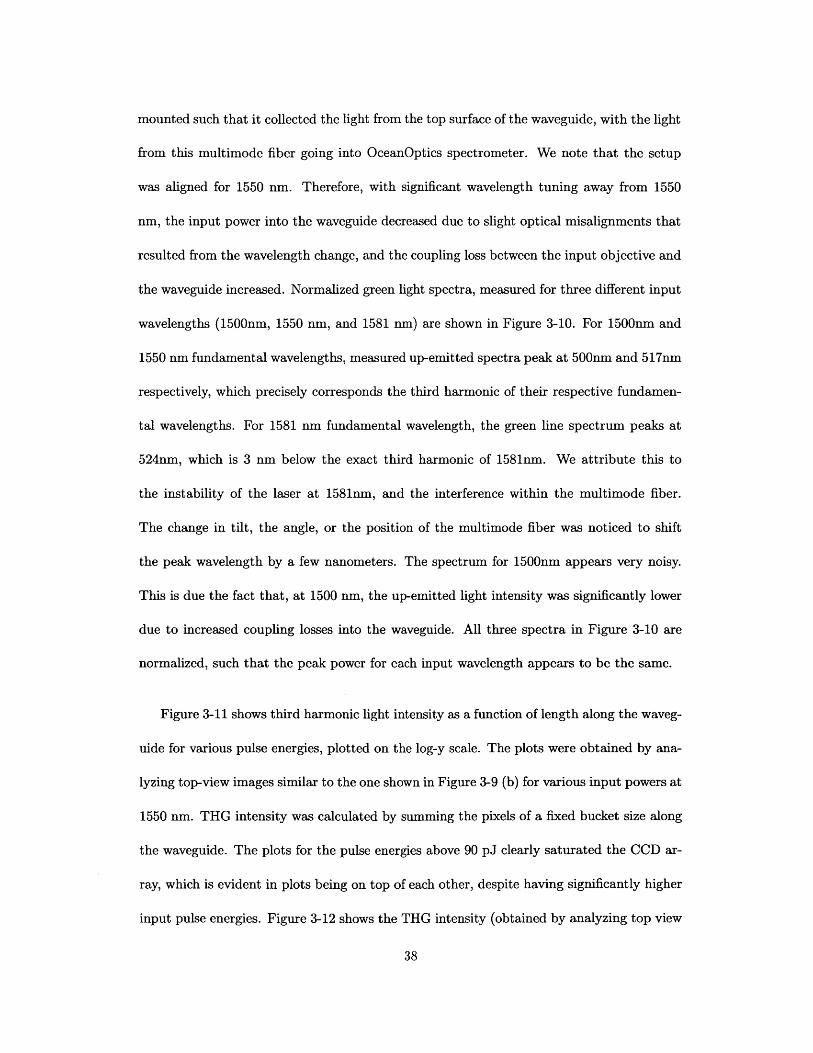
Figure 3-11 shows third harmonic light intensity as a function of length along the waveg-
uide for various pulse energies, plotted on the log-y scale. The plots were obtained by ana-
lyzing top-view images similar to the one shown in Figure 3-9 (b) for various input powers at
1550 nm. THG intensity was calculated by summing the pixels of a fixed bucket size along
the waveguide. The plots for the pulse energies above 90 pJ clearly saturated the CCD ar-
ray, which is evident in plots being on top of each other, despite having significantly higher
input pulse energies. Figure 3-12 shows the THG intensity (obtained by analyzing top view
38

Third harmonic spectrum for waveguide 2
517 524
1 ----------------------- ------- -- ----------- -----------------------
.0 .8 - -- - -- ---- - ----- -- ----------- -- -------------------2L.0.8 ---------------------- -- -E
0.6 ---------------------- ------ ----- -- - - -
$50fw 5000 55060
Waeent1550 nm
N - ,,,=1581 nmE0 0.2 ------------ - - ------ ----------
50500 550 600Wavelength, nm
Figure 3-10: Spectrum of the third harmonic lines for waveguide #2, for three input wave-length values.
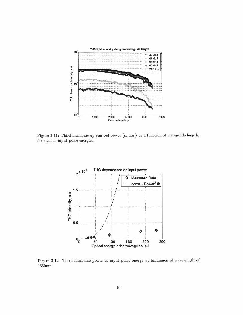
images) at some fixed point along the waveguide, vs input pulse power. Also shown is the
fit, which is proportional to the input optical power to the 3 rd power. Third order non-
linear polarization that is responsible for the third harmonic generation is proportional to
X (3)E 3(w)|, where x(3) is the third order nonlinear susceptibility, and E(w) is the incoming
electric field at the fundamental wavelength. The power generated at the third harmonic
is in turn proportional to the intensity at the fundamental wavelength cubed. The fit is
in a good agreement with experimental data for low input powers, corresponding to pulse
energies under 50 pJ. For higher values, THG intensity is significantly lower than predicted.
Among the reasons responsible for this intensity drop are the apparent saturation of the
CCD camera used to take the images for this analysis, and possibly pump depletion.
39
THG light Intensity along the waveguide length
.. .. .. .. ... .. .. ... .. .. ... .. .. ... .. .. .. ... .. .. .. .. .. . 3 7 .2 p J
.. .. .. ... .. .-. ..... .... 2 3 2 .2 pJ.
-. ............-...... ...
10
.5
10 4
10 3
4000 5000
Figure 3-11: Third harmonic up-emitted power (in a.u.) as a function of waveguide length,for various input pulse energies.
1x 1052:Xi
1.5
.
0.5
0'-0
THG dependence on input power
50 100 150 200 250Optical energy in the waveguide, pJ
Figure 3-12: Third harmonic power vs input pulse energy at fundamental wavelength of
1550nm.
40
1000 2000 3000Sample length, mrn
'U
$C0C0C
0II-
*Measured Data1 3~const x Power fit
.. . . . . . . . . . .. . . . . . .. .. . . . . . . . . . . . .. . . . . . . . .
.... ... .. . .... .. ... ... .. ... ... . ... ... .. . .... .. ... .
.... ... ... ... .. . .. ... ... ... .. ... ... ... ... ... .... ... .
0
Chapter 4
Heterodyne Pump Probe
Measurements
4.1 Theory
4.1.1 Pump-probe experiments
Femtosecond pump probe spectroscopy is a technique that allows for time-resolved studies
of nonlinear dynamics in various materials devices [31, 32, 33, 34]. This technique involves
exciting the device with a strong optical pulse (the pump), while monitoring the outcome of
this excitation with a weaker pulse (the probe). By monitoring the change in the probe pulse
as a function of time delay between the pump and the probe, it is possible to recover the
nonlinear dynamics of various devices under study. Physical models of the device dynamics
are then related to the pump-probe response curves in order to extract desired constants
and parameters. By varying the intensity of the exciting pulse (the pump), the response
of the device can be measured in both perturbational and highly nonlinear regimes. The
resolution of such experiments is comparable to the cross-correlation of the pulses used.
41

Some of the material properties that could be extracted from pump-probe experiments
are time-resolved absorption (a key measurement in characterizing saturable absorbers for
mode-locked lasers), non-linear refractive index changes, dichroism and birefringence, non-
linear absorption, and higher order nonlinearities. Depending on the desired parameters to
be measured, and on the device structure, various pump-probe experiment configurations
are used. In this work, degenerate pump-probe experiments are used, where the pump and
the probe come from the same mode-locked laser beam. When the strong pump excites
the material, and time-delayed probe is used to monitor pump-induced changes, there is a
necessity to measure only the probe beam at the output of the device, as it will contain
the material response due to pump excitation. Both the pump and the probe pulses are
incident on the device with a femtosecond relative time delay, therefore, there exist various
experimental techniques that measure the probe pulse only at the output of the device
by separating it from the pump pulse. One common method of separating the pump and
the probe is to have them orthogonally polarized with respect to each other prior to be-
ing incident on the sample. After the beams exit the device, a linear polarizer is used to
pick only the probe polarization. A common schematic of such cross-polarized pump-probe
experiment is shown in Figure 4-1.
In Figure 4-1, a mode-locked laser source is used to produce a train of optical pulses,
which is separated into the pump and the probe beams by a polarizing beam splitter (PBS).
The pump beam is time-delayed with respect with the probe beam by using a mechanical
stage with high precision motion control, which translates along the direction of the beam.
Time delay introduced into the beam is directly proportional to the distance the stage
travels. After this time delay is introduced, the pump and the probe beams are recombined
using another PBS, and are focused into the reflective sample. Yet another, third, polarizing
42

Focusing Reflective
Variable Delay lens sample
.fi PBS PBS - W/
Figure 4-1: Degenerate cross-polarized pump-probe setup in reflection.
beam splitter cube is used in front of the sample to polarization-separate reflected beams
as shown in Figure 4-1, and only the probe beam is detected. Usually the pump beam is
chopped with a mechanical chopper, and the final signal is passed from the detector to a
lock-in amplifier, which provides for background-free measurement. Since the probe beam
is not being chopped, only the photons that interacted with the pump are detected after
passing through the lock-in amplifier. This is a critical part of the experiment, which allows
to measure changes in the sample properties due to the pump-induced excitation only. By
adding extra half-waveplates into each of the paths, the intensities of the pump and the
probe can be adjusted separately.
4.1.2 Heterodyne pump-probe technique
In order to measure the response of the system in pump-probe experiments, the probe
beam needs to be separated from the pump, as mentioned in the previous section. This
could be done spatially, spectrally, or by using cross-polarized beams. However, in certain
experiments, none of those techniques lead to accurate results. One particular example is
43
measuring polarization-sensitive waveguides, where light propagation is highly dependent
on the input polarization state. In such cases, the pump and the probe often need to be at
the same wavelength, have the same polarization, and be confined in the same waveguide.
In order to provide for an accurate measurement under such conditions, a new variation
of pump-probe experiments called heterodyne technique was introduced in 1992 by Hall et
al [35, 36]. This technique uses a small frequency shift to separate the pump and the probe,
and uses a separate reference beam which beats with the probe signal on the photodetector.
In such experiments, the train of probe pulses is being separated from the pump pulses by
passing through a frequency-shifting element (usually an acousto-optic modulator (AOM)),
which shifts the pulse train by a known frequency Q1, usually in an RF band. The pump
pulse train is not shifted. A third, separate pulse train, termed a "reference" beam, which
is initially taken from the same laser source as the pump and the probe beams, is also
frequency shifted by a separate AOM by a known frequency Q2, such that the difference
Q1 - Q2 can also be detected as an RF signal. The pump and the probe beams are made
to overlap spatially and temporally in the waveguide being measured, with the pump beam
having a variable controlled time delay, as described in Section 4.1.1. The reference beam
does not pass through the sample, but is combined with the the pump/probe beams after
they propagate through the waveguide. The reference beam is path-matched with the probe
beam in order for the two beams to arrive simultaneously onto the fast photodetector. Under
such conditions, the probe and the reference beams beat on the photodetector with a beat
frequency equal to Ob = Q1 - Q2 . The polarization of the probe and the reference beams
must be the same and thus a combination of a half-wave plate (HWP) and a quarter-wave
plate (QWP) is placed in the reference beam path in order to adjust the reference beam
polarization to a desired state. Usually, to obtain background-free measurements, the pump
44

beam is chopped using a mechanical chopper. The measured signal is demodulated using
a radio receiver. The amplitude variation of the probe signal reflects the changes in pump-
induced material absorption, and the phase variations of the demodulated probe signal
reflect the phase changes induced in the sample.
The pump, the probe, and the reference beams can be represented as follows:
Epump = Re {E(t + r)c(t)ejw(t+) } (4.1)
Eprose = Re {E(t)e3(Wif )t}
Eref = Re {E(t)e(W-2)t}
In Equation 4.2, Epump, Eproe, and Eref are the electric fields of the pump, the probe,
and the reference beams respectively. Q1 and Q 2 are AOM-induced frequency shifts on the
probe and the reference beams, r is variable time delay, and c(t) is the chopping frequency.
This representation ignores the polarization of the beams, and their relative amplitudes.
The electric field at the input of the waveguide is the sum of the pump and the probe
beams, and is written as:
Ein = Epump + Eprobe (4.2)
The response of the heterodyne pump-probe experiment is the relative change in phase
(for PM measurement) or in intensity (in AM measurement) of the probe beam. For sim-
plicity, we will show the theory for the intensity measurement, however, the analysis of the
material response presented in this section is identical for the phase measurement. The time
derivative in a nonlinear change to material polarization P is written according to Equation
45
4.3, where hijkl is a tensor material response to the total input electric field polarization
components Ej, Ek, and El. hijk can be related to the third order nonlinear susceptibility
(3)
Xijkl*
t dt 3Ej(t)higk1(t - t")Ek(t")E1 (t") (4.3)
The change in optical intensity on the probe beam due to the pump beam can be written
according to Equation 4.4, where d is a constant, and AP is the change in nonlinear pump-
induced material polarization, given by Equation 4.3.
AI = jdtRe E - t} (4.4)
The quantity measured by a heterodyne pump-probe experiment is AI/I in AM mode
(absorption change) or Ab/<} in PM mode (phase change).
4.1.3 Coherent Artifact
In order to get a full expression of the material response to the pump-probe input electric
fields, Equations 4.2, 4.2, and 4.3 need to be substituted into Equation 4.4 with correct
polarizations [37]. The result will consist of many terms, including pump-induced changes
on the pump beam, probe-induced changes on the probe beam, probe-induced changes on
the pump beam and pump-induced changes on the probe beam. Since the experiment
measures the heterodyne beat signal of the probe and the reference, and terms that result
in changes on the pump beam can be ignored. In addition, probe-induced changes on the
probe beam are typically very small, since the probe beam power is usually at least 6 dB
less than the pump power. Thus, probe-induced changes on the probe beam terms will also
46

be ignored. We will consider only the terms that include pump-induced changes on the
probe beam, when the pump and the probe have parallel polarizations, which is the case in
our experiments. The resulting change in probe intensity can be written as a sum of two
terms [31, 37]:
AI. b(71 + #11) (4.5)
0||(r) = dtdt'IE1(t - r)| 2 hxxX (t - t')|E1 (t)12
#31(7-)= dtdt'E* (t - r)E 1 (t)hxxxx (t - t')- r )
where the field delayed by r is the probe, and other other one is the pump. The term
7l(r) is a material response convolved with a second order correlation function (optical
intensity), so it is the material response to the pump field, exactly what we are trying to
measure. The term #1 (r) constitutes a coherent coupling between the pump and the probe
beams at zero time delay. It is evident from #il (r) expression that #|| = 0 when there is no
overlap between the pump and the probe beams. Upon further examining Equation 4.5, it
is evident that at zero time delay between the pump and the probe, #11 (r = 0) = -y (r = 0),
which means that at zero time delay, half of the measured HPP response is due to the actual
material response, and another half is due to the coherent artifact. Therefore, all the data
must be normalized to account for this.
47

4.2 Experimental Setup
The schematic of the experimental setup of the heterodyne pump-probe experiment used
to measure TiO 2 devices is shown in Figure 4-2. The optical beam starts with Spectra
Physics optical parametric oscillator (OPO) OPAL pumped by titanium-sapphire MaiTai
laser. The resulting beam is a 80 MHZ train of optical pulses, centered at 1550 nm, with
pulse duration of - 180fs. The beam passes through a half-waveplate and a polarizing
beam splitter cube (PBS1 in Figure 4-2), which separates the probe beam and the future
pump/reference beam. HWP-PBS combination allows to tune the power in both beams.
The probe path passes through an AOM, and is upshifted by Q1=36.7MHz. The beam then
goes through another HWP (which allows to tune the power in the probe beam incident on
the sample independently from the pump/reference beam powers), and is recombined with
the pump using a 50/50 beam splitter cube. The pump beam, after passing through PBS1 ,
goes through another HWP/PBS combination, which separates it into the pump and the
reference beams. The pump is reflected off PBS2 as shown in Figure 4-2, passes through a
mechanical chopper (Qc=1.3kHz), a variable time delay stage, another HWP, which allows
to tune the pump power incident on the sample independently, and is combined with the
probe beam in a 50/50 beam splitter. Combined pump and probe beams pass through PBS3
in order to ensure they have the same exact polarization state, followed by a combination of
QWP and HWP for polarization tuning, and are coupled into TiO2 waveguide using a free
space objective. An identical free space objective couples the light out of the waveguide into
the 50/50 fiber splitter, which combines the pump-probe beam with the reference beam.
The reference beam, after being separated from the pump at PBS2, passes through another
AOM, which upshifts the beam by Q2 =35MHz, followed by a variable time-delay stage
which allows to match the reference and the probe path signals, in order to overlap the two
48

on the fast photodetector. This beam then goes through a QWP/HWP combination, is
coupled into an SMF28 optical fiber, and is combined with the pump and the probe beams
using a 50/50 fiber power splitter/combiner. One output of this power splitter is used to
monitor the optical power in either one of the beams, while the other end is directed into
a fast photodetector. The probe and the reference beams beat at the photodetector with
Qb = Q1 - 02 = 1.7MHz. A low pass RF filter follows the photodetector and cuts off
all the RF frequencies above 1.9 MHz. The RF signal from the photodetector goes into
the IC-R71A Ham radio, which can be set at either AM or FM mode depending on the
measurement type. The demodulated signal from the Ham radio is directed into the lock-in
amplifier, which locks onto the pump chopping frequency, and thus detects only pump-
induced changes on the probe-reference beat signal. In order to couple the light into and
out of the waveguide, two identical free space objectives were used (60X,NA=0.85). We
note that prior to entering the TiO2 waveguide, both the pump and the probe beams travel
using free space optics, which adds negligible dispersion to the optical pulse. An acousto-
optic modulator in the probe path does not add significant dispersion to the probe beam
either. In order to get a proper beat signal at the photodetector, both the reference and the
probe beams are length matched, and polarization matched. This is done by first varying
the QWP/HWP combination in the pump-probe path in order to find the polarization
state best supported by the device, and then varying the QWP/HWP combination in the
reference path in order to match the polarization at the output of the TiO 2 waveguide.
When polarization states of the probe and the reference beam are identical, the strength of
the beat signal on the detector is maximum.
Since the Ham radio is used in order to demodulate the signal, it is necessary to properly
calibrate the radio to make sure it operates in the linear regime. This is done using the
49

Fixed delay(T)
Figure 4-2: Heterodyne pump-probe setup.
following procedure: first, the level of the probe-reference beat signal is measured. Second,
a separate RF signal of the same level as the probe-reference beat signal is created by a
separate signal generator, and varying degrees of AM and FM modulation level are applied
to this RF signal externally. The response of the radio in AM/FM regimes should scale
linearly with linear change in AM/FM modulation depth on the signal. The level of the RF
signal going into the radio is therefore attenuated until the response of the radio is linear
for 100% AM and 300% FM modulation depths.
Separately, the radio is checked for any undesired AM/FM conversion. Both RF and
AF gains on the radio are adjusted until a 100% AM modulated signal shows no component
in FM demodulation, and a 100% FM modulatated signal shows no component in AM
demodulation.
50

4.3 Characterizing coupling losses
The response of the waveguide to the excitation by an ultrafast pulse depends on the light
intensity inside the waveguide. Our experimental setup lets us measure the light power
prior to entering the input objective (by using a free space power meter), and after exiting
the output objective (by using fiber-coupled power meter). Thus, the actual light power
inside of the waveguide is not known, and needs to be determined by carefully analyzing the
coupling losses. While it is most simple to assume that our input and output coupling losses
are equal, careful previously demonstrated analysis has shown that the difference of such
coupling losses may be as large as 4 dB [2, 38]. In addition, it was visually observed that
our particular waveguides were not cleaved properly, and the input and output facet cleaves
differed significantly when observed via microscope. Therefore, it is important to separate
the input and the output coupling losses and determine them without the assumption that
they are equal.
A schematic that visualizes coupling losses is shown in Figure 4-3. The optical beam
enters the waveguide, with optical power right before the waveguide being Pi", in dBm.
Optical power after exiting the waveguide is measured to be Pot, also in dBm. C1 is the
fractional input coupling loss, measured in dB, and C2 is the fractional output coupling
loss, measured in dBm. When the direction of light propagation is changed, C2 becomes
the input loss, and C1 becomes the output loss, but they retain the same fractional value.
With no nonlinearities present, the losses can be described according to Equation 4.6, where
a is a linear loss in dB/cm, and L is the device length in cm. The sum of coupling losses
can then be determined by measuring the input and output power in the linear regime,
according the Equation 4.7. In order to calculate coupling losses individually, another,
different equation, relating C1 and C2 is necessary.
51

out Pout, wg inwg in
C2 C1
Figure 4-3: Schematic of coupling losses in and out of the waveguide.
Pat = Pi. - C1 - C2 - aL (4.6)
C1 + C2 = Pin - Pt - aL (4.7)
In a similar work performed on the silicon nanowaveguides by A. R. Motamedi [38], the
coupling losses have been separated using two photon absorption nonlinearity. The power
transmitted through any particular waveguide would decrease and deviate from the linear
response on a log-log scale as the input power is increased to the point where two photon
absorption effects become significant. The level of this two-photon absorption depends on
the optical power inside of the waveguide. The experiment is performed in two directions,
with light propagating through the waveguide right-to-left, and left-to-right, and the two-
photon-absorption-dependent loss is measured in each case. The difference between two
power values for two measurement directions that exhibit the same two-photon absorption
corresponds to the difference in the input and output coupling losses.
TiO2 waveguides used in this experiment do not support two photon absorption at
1550 nm, and thus it can not be used to separate coupling losses. The only other way to
measure such coupling losses is to use some other type of nonlinearity, that is dependent on
the light intensity inside of the waveguide. In this work, we will use pump-induced phase
52

modulation of the probe beam as such nonlinearity. In fact, the main normalized heterodyne
pump-probe response curve from PM measurement is exactly the data that will be used to
characterize coupling losses. Figure 4-4 (a) shows PM heterodyne pump-probe traces for
the light propagation from left to right, for various input power levels. The maximum peak
in each curve corresponds to point where the probe and the pump pulses have maximum
time-overlap. The peak value on each curve corresponds to the maximum phase modulation
induced by a certain light intensity inside of the waveguide. The PM heterodyne pump-
probe experiment was subsequently repeated with light propagating right-to-left through
the same waveguide. The results are shown in Figure 4-4 (b). Figures 4-4 (a) and (b) show
the same experiment, with exactly the same input pump power, performed in two different
directions. It is evident from the two plots that, for the same input pump power, the
maximum phase modulation on the probe signal is lower for right-to-left light propagation
experiment. This can be explained with the difference in coupling losses - for the right-
to-left direction, the input coupling loss is greater than the input coupling loss for the
left-to-right light propagation. Thus, the difference between coupling coefficients C1 and
C2 can be extracted from Figures 4-4 (a) and (b). We note that careful optical alignment
is performed in those experiments to ensure that the same amount of light enters the input
objective in either light propagation direction, and that the amount coupled in is maximized.
53

'4
0
0.08
0.06
0.04
0.02
0
Unprocessed PM HPP traces for TiO2, wg4.
Probe power -3.05 dBm,for left-to-right light propagation
i------
0 1000 2000 3000 4000 5000 6000is
(a) HPP PM measurement traces, unprocessed, for for left-to-right light propagation.
Unprocessed PM HPP traces for TiO 2 , wg4.
Probe power -3 dBm,for right-to-left light propagation
In
0
0.08
0.06
0.04
0.02
0
----------- - .-.------ .- . ----. --.
------ ----.. ---------..- .---------.
0 1000 2000 3000 4000 5000fs
6000
(b)HPP PM measurement traces, unprocessed, for right-to-left light propagation.
Figure 4-4: Heterodyne pump-probe PM measurement traces, unprocessed, for for left-to-
right (top) and right-to-left (bottom) light propagation direction.
54
-14.1403 dBm pump in- 13.0103 dBm pump in-- 12.0103 dBm pump in
11.0103 dBm pump in-10.0103 dBm pump in
-- 9.0103 dBm pump in
--14.1403 dBm pump in- 13.0103 dBm pump In
12.0103 dBm pump In11.0103 dBm pump in10.0103 dBm pump in
-9.0103 dBm pump in
-
............................
...........

In order to extract the difference between the coupling coefficients from the phase modu-
lation heterodyne pump-probe measurements, we first plot the maxima of the HPP response
versus input pump power (the peak of each plot in Figure 4-4 vs input pump power). This
is shown in Figure 4-5 (a). This maximum HPP response (maximum phase modulation) is
proportional to the change in optical phase. This change in optical phase is shown in Figure
4-5 (b), with the detailed calculations of the phase from maximum HPP phase modulation
response curves explained in Section 4.4. Next, the procedure is to find the points on the
left-to-right curve of Figure 4-5 that have exactly the same phase modulation as the points
on the right-to-left curve. In order to do that, both curves are extrapolated to have more
data points, and Matlab algorithm is used to find the desired points, which are shown in
Figure 4-6 with large black crosses. At such points, the change in optical phase is the same
for both light propagation directions; therefore, optical intensity inside of the waveguide
must also be the same for both directions of propagation. Since the points of equal optical
phase change corresponding to two light propagation directions clearly correspond to differ-
ent input optical power, the difference between this input optical power for two propagation
directions must come from the difference in coupling losses.
55

TlO 2 heterodyne pump probe max PM change, w9 #40.07
> 0 .0 6 .. ....... ............... ........ ... .......
CL0 . .. .. . .. . . .. . .. . .. .. . . .. . .. .. . .
a 0 .0 5 ...... ............ ........ ......1
0 .0 . . . . .. . . . .. .. . .. .. . .. . .. . ... . .. .
~0 .0 . .............. ......... ....
.......0.0 00004
12Pump0 , dBm
(a)
0.25
0.2
5 0.15
S0.1
A + for 102, wg #4, for PM HPP measurementProbe power -3.05 dBm
-5 10 15 20Pump0 , mW
(b)
Figure 4-5: (a) Maximum response of the heterodyne pump-probe PM measurement forleft-to-right (LR) and right-to-left (RL) light propagation directions. (b) Maximum probephase change due to pump-induced index change, for left-to-right (LR), and right-to-left(RL) light propagation directions.
A + for TiO2, wg4, for heterodyne pp measurementProbe power -3.05 dBm
35
C0
CaI.-.
0.3
0.25
0.2
0.15
0.1
0.05
0
+giLR
- -RL ------------ ------------ ------------ ----------
- LRfit:RLfit ------- r---
------------ fit -------------------- -------- - --- --
- -- ------------ ------------ ------ --- -- - ------ -- ------
------------ +------------+---- ---+-----------
--------- - C 2 C 1-- - ----
6 8 10 12 14 16Pump dBm
Figure 4-6: Determining C2 - C1 from maximum phase change on HPP response curved for
two directions of light propagation. Black crosses / lines show points of equal phase change
in both directions of light propagation.
56
25 30
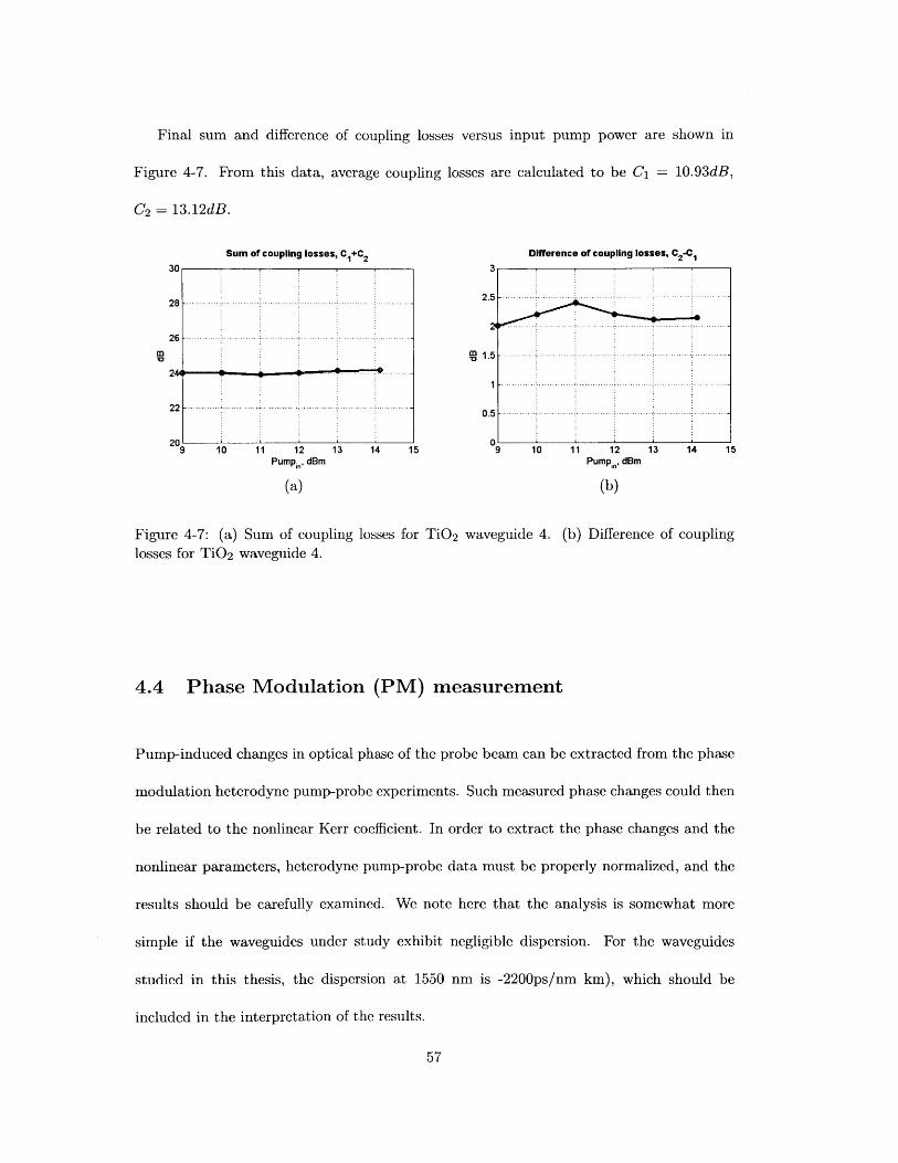
Final sum and difference of coupling losses versus input pump power are shown in
Figure 4-7. From this data, average coupling losses are calculated to be C1 = 10.93dB,
C2 = 13.12dB.
Sum of coupling losses, CI+C 2
-- 0- - . -- - 1 - -- 3 -
..................- -.. ........ --.. .......... .
Difference of coupling losses, C 2-C
10 11 12 13Pump, dBm
(a)
2.5
i 1.5
1
14 15 9 10 11 12Pump,. dBm
(b)
Figure 4-7: (a) Sum of coupling losses for TiO2 waveguide 4. (b)losses for TiO2 waveguide 4.
Difference of coupling
4.4 Phase Modulation (PM) measurement
Pump-induced changes in optical phase of the probe beam can be extracted from the phase
modulation heterodyne pump-probe experiments. Such measured phase changes could then
be related to the nonlinear Kerr coefficient. In order to extract the phase changes and the
nonlinear parameters, heterodyne pump-probe data must be properly normalized, and the
results should be carefully examined. We note here that the analysis is somewhat more
simple if the waveguides under study exhibit negligible dispersion. For the waveguides
studied in this thesis, the dispersion at 1550 nm is -2200ps/nm kin), which should be
included in the interpretation of the results.
57
in
28
26
244
22
2013 14 15
-.. ...... ... .. --.. .. -.. .. .. -.. .... ......
- -- -.----.--.-.--.-- ...................-. ......-- -------.-. --

4.4.1 PM normalization
Figure 4-2 shows the schematic of the heterodyne pump-probe experiment. In phase mod-
ulation experiment, the HAM radio is set to FM mode, such that it extracts the frequency
modulation of the probe signal induced by the pump signal. The lock-in amplifier inte-
grates the signal over time, and provides background-free measurement by using the pump
chopping frequency as a reference signal. Time-integration converts frequency modulation
into phase modulation, which is used to obtain the nonlinear refractive index. The units
of the unprocessed data coming out of the lock-in amplifier are mV. In order to convert
mV to fractional change in optical phase, a careful calibration of the setup is performed to
determine the phase modulation reference signal. For angular modulation, the modulation
index is defined according to Equation 4.8, where Af, is the maximum frequency deviation,
fm is the frequency of the modulating signal, and A4, is phase change in radians. In order
to obtain one radian, the Af, must be equal to fm,. In heterodyne pump probe experiments,
the modulating frequency is the frequency that the pump is being chopped at, in our case,
1.3kHz. Thus, for 1 radian of phase change, 1.3kHz of maximum frequency deviation must
be applied to the signal.
mFM =f = AOp (4-8)fm
This calibration is done according to the following procedure:
1. The pump beam is blocked
2. The AOM that frequency-shifts the probe beam is driven by an RF source with
Q = 36.7MHz, as for the normal experiment, however, the 36.7 MHz carrier going
into the AOM is also modulated by the square wave at a frequency of fm=1.3kHz,
58

which coincides with the pump chopping frequency; and Afy, the maximum shift of Q,
is set to 1.3kHz, in order to provide 100% FM signal, or 1 radian of maximum phase
modulation. This provides 100% phase modulation (or a maximum phase change of
1 radian) of the optical signal.
3. This 100% FM modulated probe signal beats with the reference signal. The beat
signal is directed into a fast detector, which directs the RF beat signal (at 1.7MHz)
into the HAM radio, set for FM demodulation mode, with a carrier frequency set to
1.7MHz.
4. The output of the radio is directed into the lock-in amplifier, which takes the 1.3kHz
modulating frequency as a reference.
5. The resulting R value from the lock-in amplifier is used as a 100% PM (1 radian)
reference value.
Figure 4-8 shows the 100% FM modulated beat note of the probe and the reference,
as a result of this normalization. The signal was measured at the fast detector collecting
probe/reference beat note. In this Figure, the central beat peak is at 1.7MHz, and the
side bands are separated from each other by 1.3kHz, which is the modulating frequency,
equal to the chopper frequency. The height difference of the adjacent peaks refelects the
level of the FM modulation, and can be analytically calculated for any mFM value [39].
Although an identical trace could be obtained through heterodyne pump-probe experiment
with an appropriate amount of input pump power, we found that, with measured material
nonlinearity values, the maximum pump power level available in the setup was not enough
to exceed 0.3 radians of phase change, far from 1 radian obtained through this calibration.
Since neither the reference nor the probe power levels change throughout the experiment,
59

this 100% probe phase modulation is independant of the input pump power, and is used
to normalize all the PM heterodyne pump-probe traces. After normalization, the hetero-
dyne response is the fractional pump-induced phase change(A$) on the probe. Figure 4-9
shows a heterodyne pump-probe trace, fully normalized, accounting for the coherent artifact
described in Section 4.1.3, versus pump power in the waveguide.
Beat signal of the 100% FM modulated probe beam with the reference beam70
..85 ------ ------ ------ ----- ---- - ---- -------- - ---- I ---- ----
115
-85 1-- ---- -- -- - -- --- -- -- -
1.69 1.692 1.694 1.696 1.698 1.7 1-702 1.704 1.706 1.708 1-71MHz
Figure 4-8: RF beat signal of 100% FM modulated probe beam andused for PM normalization.
Phase change vs pump power in the waveguide0.25
0 .2 -------------- -------------. -------------. ----------. ----. ---------------
0 .1 5 ---------------- -. .... ...-------------- --- -- -- - ..-------------- ---------------.
0 .0 5 ---- ---- --- . - - - - - -- - - - - -- - - - - - -- - - - - -- - -- - -- - - - - -
0.5 1 1.5 2Pump power in the waveguide, mW
the reference beam,
2.5
Figure 4-9: Normalized heterodyne pump-probe material response for PM measurement,
versus pump power in the waveguide
60
4.4.2 Calculating nonlinear index of refraction from A0.
The heterodyne pump-probe experiment measures changes in optical phase of the probe
beam, induced by the pump beam. Equation 3.2 relates this change in optical phase to the
nonlinear refractive index coefficient n2 , assuming no dispersion. Thus, n 2 can be written
according to Equation 4.9, where AO is the center wavelength of the laser in vacuum, I is
the effective light intensity inside of the waveguide, AO is the peak phase change due to
nonlinearity, and Leff is the effective length of the interaction, which takes into account
linear losses of the material. For negligible dispersion, the effective length is calculated
according to Equation 4.10, where L is the physical length of the device, and a is the linear
loss. For the TiO2 devices measured in this thesis, a = 8dB/cm, and L=9.2mm, which
gives the effective length of 4.43mm.
n2 = A4$ ( (4.9)I 2,7r Leff
1 - (410Leff = (4.10)
a
The effective intensity of the optical beam is calculated by dividing the peak pulse
power by the effective area. For sech2 pulse shape, the peak power is calculated from the
average power as follows: Peak = 0.88 , where R is the repetition rate of the laser, and
r,, is the FWHM pulse width. Because the devices measured exhibit significant amount
of normal dispersion, the pump and the probe pulses broaden inside of the waveguide.
The effective pulse width, to be used in the calculations, can either be determined from
the split-step analysis, or estimated from the heterodyne pump-probe plots. Figure 4-
4 shows unnormalized HPP traces, where each trace can be describes as a convolution
61

of the intensity autocorrelation with the material response (as described by al term in
Equation 4.5). Assuming instantaneous material response, the heterodyne pump-probe
traces can be thought of as scaled versions of the intensity autocorrelation. We estimate
the FWHM nonlinear effective duration of the pulse from the intensity autocorrelations
to be ~ 260fs on average. In comparison, optical pulses at the input of the waveguide
have a FWHM duration of 180fs; therefore, the measured pulse duration of 260fs indicates
the definite pulse spreading inside of the waveguide, which affects the nonlinear phase. In
order to take into account for the dispersion in the waveguides, we therefore use the pulse
duration of 260fs in order to calculate optical intensity, when using the Equation 4.9 to
calculate nonlinear refractive index. The effective area of the optical mode for the nonlinear
interaction is calculated according to the following formula [40]:
Z 2 jf f Re {E(x, y) x H*(x, y)} -ezdxdy 2
Aef = -' (4.11)ncore ffcore|E(x,y)4 dxdy
This formula assumes that the nonlinearity is limited to, and is uniform over, the core
of waveguide. In low-index-contrast devices, Equation 4.11 reduces to a more standard
effective area definition [41].
For the TiO 2 devices measured in this work, Aeff was calculated to be 0.373 pm2.
We note that the pump-probe experiment measures the average change in optical phase,
where the measured phase change is the result of the time-overlap integral of the pump
and the probe, weighted by the peak phase change. Equation 4.9 assumes A# is the peak
phase change, not the average phase change. Taking into the account the time-overlap
integral of the sechant hyperbolic pulses weighted by the peak phase change, the measured
phase change is about a factor of two less than the peak phase change. Figure 4-10 shows
Aopeak versus optical intensity inside of the waveguide, where the intensity is in units of
62

W/cm 2 x 10¹⁰. The slope of this measured curve is the proportionality constant between
A# and n2: A# = slope x n2. This slope, extracted from the linear fit in Figure 4-10, was
used to calculate nonlinear refractive index n2, which is found to be 1.03 x 10- 15 cm 2 /W.
A vsl for wg #4, RL0.5
0 .4 ---------------- .. ..-------- ..------ ..--- ..-.- ..------- ..-- .-.----- .- ..------
0 .3 ---------------. -------- .... .. ... .. .... ------ ----. ---- ------.----- ---- --- .
0 .1 ----- .. .. .. ----------... ---- ---- - .-- ---- ----.-.11X"..Measured
Linear fi
0.5 1 1.5 2 2.5Intensity inside the waveguide, in W/cm2 0
Figure 4-10: Measured nonlinear peak phase change versus peak optical intensity inside of
the waveguide
In our calculations, we assumed that Equation 4.9 could be used for calculating optical
Kerr coefficient in waveguides with significant amount of dispersion, provided that the
pulse duration used for calculations is the dispersion-broadened value. In order to verify
that such calculations are correct, we run the split-step simulation code [34] (see code
attached in Appendix), that takes into account both nonlinearity and dispersion. The split-
step code starts with a pulse width of -r,=180fs, and the average input pump pulse energy
equal to 26.2pJ (corresponding to the actual input power in the waveguide). The code
then step-by-step propagates the pulse through the duration of the waveguide, adding the
nonlinearity in the time domain and the dispersion in the frequency domain. With n2 =
1.03 x 10- 15cm 2 /W, we get the maximum peak nonlinear phase shift of 0.45 radians, which
63

agrees very well with the measured peak nonlinear phase change of AO$ = 0.441 radians, as
shown in Figure 4-10. Moreover, the pulse duration at the end of the effective length period
of the waveguide (i.e. at 4.43 mm point) also agrees with the measured pulse duration.
We therefore conclude that according to our heterodyne pump probe measurements, the
optical Kerr coefficient of anatase is measured to be 1.03 x 10- 15cm 2 /W.
4.5 Amplitude modulation (AM) measurement
Heterodyne pump-probe AM measurements detect changes in the probe signal amplitude
that are due to the pump-induced nonlinear absorption. Multi-photon absorption is a non-
linear process, which depends on the input signal power. Usually, if the material energy
gap supports two-photon absorption, a heterodyne pump probe experiment allows to deter-
mine the TPA coefficient, along with TPA-induced free-carrier absorption (FCA). We note
that TiO2 devices studied in this thesis do not support two-photon absorption at 1550nm,
and thus, no AM signal was detected at the output of the waveguide. To confirm this, we
present a brief analysis along with one trace showing no AM signal for the highest input
pump power supported by the setup.
4.5.1 AM normalization
AM measurements in heterodyne pump-probe experiments need to be normalized to the
AM reference level. The degree of modulation m, for an AM signal, is defined according to
Equation 4.12 below, where Emax is the maximum signal amplitude, and Emin is the mini-
mum signal amplitude. With 100% AM modulation, m=1, and the signal goes completely
on and off at the modulating frequency. The reference level is obtained by blocking the
pump, and chopping the probe beam instead at the pump chopping frequency (1.3kHz in
64

our experiment). The chopper, with 50% duty cycle, creates 100% AM modulation at the
chopping frequency. The response of the HAM radio in the AM regime to the beat signal
of the reference beam and the chopped probe beam is fed into the lock-in amplifier, which
uses the chopping frequency as a reference signal. The value from the lock-in amplifier is
used as a reference level for the AM measurement. Figure 4-11 shows the RF beat signal
for the probe and the reference with 100% AM modulation used to determine the reference
level. For AM modulation, the sidebands are separated from each other by the modulating
frequency, which is evident in Figure 4-11, where the sidebands are separated from the car-
rier of 1.7MHz by fm=1.3kHz. In addition, for 100% AM modulation, the sidebands closest
to the carrier (at fc ± fi) are 6dB lower than the carrier level, which is well indicated in
Figure 4-11.
Emax - Emin
Emax + Emin
E
-81
-94
-9
-101
-10
-11
-1 1
Probe-reference beat signal with 100% AM modulation
5------------------ ------ ------------ ------------------ -----------------
1.3kHz------------------ -~-- --- ----------- -----------------
6dB5 ----------------- - ---- ------------ -----------------
0----------------- ----------- -- -- ------------ -----------------
5 ------------------ -- ------- - - ------ --- -----------------
0----------------- -----------------I ---------------- -----------------5
.69 1.695 1.7MHz
1.705
(4.12)
1.71
Figure 4-11: Probe-reference beat signal at 100% AM modulation, used
reference level.
to determine AM
65

4.5.2 Nonlinear absorption
Since the devices used in this work do not support two-photon absorption, no distinguishable
AM trace was detected. An example of the measured heterodyne pump-probe trace in AM
regime for TiO2 waveguides, equivalent to Figure 4-4 of the FM regime, is shown in Figure
4-12 (a). As a comparison, an AM HPP measurement on silicon nanowaveguides, which do
exhibit TPA at 1550nm, is shown in Figure 4-12 (b) [2, 38]. In this Figure, it is evident
that the magnitude of the AM response is proportional to the input pump power. The
greater the input pump power, the greater the TPA-induced loss, visible as a signal drop at
zero time-delay. In fact, the AM response from this Figure consists of two components - the
instantaneous response, proportional to TPA coefficient, and the slow response, proportional
to the free carrier absorption (FCA). The depth of this signal at zero time delay can be
used to extract TPA coefficient 3, and the slow time response can be related to the FCA
effective cross-section, as shown in [2].
66

Hetrodyne pump-probe AM response for TiO2 wg4ix 10
0 1000 2000 3000fs, time delay
(a)
4000 5000
-
-- 9dBm--- 12dBm
-- 16.5dBm
0 10 20 30Delay (ps)
(b)
40 50 60
Figure 4-12: (a) AM response of the TiO 2 waveguide 4, shows no signal - no nonlinearabsorption. (b) AM response of a silicon nanowaveguide, courtesy of A. Motamedi [2],shows a strong AM response due to a large TPA coefficient.
67
8
0
IS-0.3
j-0.4E-0
..................................................................... .................
................ ............. ........ .................
................. : ......... ....... .............. ..................................
... .. ... .. .
-0.1-
-0.6 -

68

Chapter 5
Conclusion
For this thesis we have measured the optical Kerr nonlinearity of anatase titanium dioxide
waveguides. We have used both the self-phase modulation method and heterodyne pump-
probe methods to determine this nonlinearity. The SPM method resulted in n2 = 1.82 x
10- 15cm 2 /W, while heterodyne pump-probe method resulted in n2 = 1.03 x 10- 15cm 2 /W,
which is a factor of 1.767 smaller than the SPM-measured value. Since the same waveguide
was measured in two experiments, the values should not differ by such a large factor. In
order to double-check the values measured, the identical split-step code was used in order to
calculate the nonlinear phase shift for both experiments. The input pulse energy that was
used in SPM experiment was used with SPM-measured n2 value, and separately the input
pulse energy that was used in HPP experiment was used with HPP-measured n2 value. We
found that in each case the split step code confirmed the maximum phase change directly
measured by the experiment, which proves that each experiment is self-consistent. Table 5
summarizes the results of the experiments and the split-step code analysis.
Further studies are necessary to determine whether the optical Kerr coefficient of anatase
TiO2 is closer to 1.82 x 10- 15cm 2 /W, or to n2 = 1.03 x 10~1 5cm 2/W. If the true value for
69

Input Input n 2 Measured Calculatedpulse energy intensity Apeak AOpeak
pJ W/mz cm 2 /W radians radians
HPP 26.2 0.245x 10¹⁵ 1.03 x 10⁻¹⁵ 0.44 0.451SPM 229 3.0x10 15 1.82 x 10⁻¹⁵ 1.57r 1.57r
Table 5.1: Final results from both heterodyne pump-probe(HPP)broadening/self-phase modulation (SPM) experiments.
and spectral
anatase TiO2 n2 is closer to the SPM-measured value, this makes the material comparable
to silicon nitride, and the nonlinearity is indeed an order of magnitude higher than that of
silica glass. On the other hand, if the true n2 value is closer to that measured by heterodyne
pump-probe experiment, this may make the anatase TiO2 slightly less attractive. Future
experiments are planned to resolve this difference.
70

Bibliography
[1] C. C. Evans, J. D. B. Bradley, J. Choy, 0. Reshef, P. B. Deotare, M. Loncar, and
E. Mazur, "Submicrometer-width TiO 2 waveguides," Proc. CLEO: Science and Inno-
vations, (San Jose, CA), May 2012.
[2] A. R. Motamedi, A. H. Nejadmalayeri, A. Khilo, F. X. Kartner, and E. P. Ippen,
"Ultrafast nonlinear optical studies of silicon nanowaveguides," Optics Express 20(4),
pp. 4085-4101, 2012.
[3] M. Dahlem, Studies of advanced integrated nano-photonic devices in silicon. PhD thesis,
Massachusetts Institute of Technology, 2011.
[4] M. Salib and et al, "Silicon photonics," Intel Technology Journal, pp. 1-20, May 2004.
[5] W. Green, S. Assefa, A. Rylyakov, C. Schow, F. Horst, and Y. Vlasov, "CMOS in-
tegrated silicon nanophotonics: Enabling technology for exascale computational sys-
tems," Invited talk at the SEMICON Conference, (Tokyo, Japan), December 2010.
[6] Y. A. Vlasov, "Silicon CMOS-integrated nano-photonics for computer and data com-
munications beyond 100G," IEEE Communications Magazine, pp. 567-572, February
2012.
71
[7] A. Khilo and et al, "Photonic ADC: Overcoming the bottleneck of electronic jitter,"
Optics Express 20(4), pp. 4454-4469, 2012.
[8] Q. Lin, J. Zhang, G. Piredda, R. W. Boyd, P. M. Fauchet, and G. P. Agrawal,
"Dispersion of silicon nonlinearities in the near infrared region," Applied Physics Let-
ters 91(021111), 2007.
[9] Q. Lin, 0. J. Painter, and G. P. Agrawal, "Nonlinear optical phenomena in silicon
waveguides: Modeling and applications," Optics Express 15(25), pp. 16604-16644,
2007.
[10] 0. Carp, C. L. Huisman, and A. Reller, "Photoinduced reactivity of titanium dioxide,"
Progress in Solid State Chemistry 32, pp. 33-177, 2004.
[11] S. J. Wang, W. T. Chang, J. Y. Ciou, M. K. Wei, and M. S. Wong, "Preparation of
TiO 2 thin films by laser ablation for photocatalytic applications," Journal of Vacuum
Science and Technology A 26(4), pp. 898-902, 2008.
[12] A. Fujishima, T. N. Rao, and D. A. Tryk, "Titanium dioxide photocatalysis," Journal
of Photochemistry and Photobiology C 1(21), pp. 898-902, 2000.
[13] A. Fujishima and X. Zhang, "Titanium dioxide photocatalysis: present situation and
future approaches," Comptes Rendus Chimie 9(5-6), pp. 750-760, 2006.
[14] J. N. Clifford, E. Martinez-Ferrero, and E. Palomares, "Dye mediated charge recombi-
nation dynamics in nanocrystalline TiO2 dye sensitized solar cells," Journal of Mate-
rials Chemistry 22(12), pp. 415-422, 2012.
[15] I. Haeldermans, K. Vandewal, W. D. Oosterbaan, A. Gadisa, J. D'Haen, M. V.
Bael, J. V. Manca, and J. Mullens, "Ground-state charge-transfer complex forma-
72
tion in hybrid poly(3-hexyl thiophene):titanium dioxide solar cells," Applied Physics
Letters 93(223302), 2008.
[16] H. A. Maclead, Thin-film optical filters, CRC Press, Boca Raton, Florida, 2010.
[17] J. D. B. Bradley, C. C. Evans, J. T. Choy, 0. Reshef, P. B. Deotare, F. Parsy, K. C.
Phillips, M. Loncar, and E. Mazur, "Submicrometer-wide amorphous and polycrys-
talline anatase TiO2 waveguides for microphotonic devices," Optics Express , 2012.
Submitted for publication.
[18] C. C. Evans, J. D. B. Bradley, E. A. Marti-Panameno, and E. Mazur, "Mixed two-
and three-photon absorption in bulk rutile TiO2 around 800 nm," Optics Express 20,
pp. 3118-3128, 2012.
[19] H. Long, G. Yang, A. P. Chen, Y. H. Li, and P. X. Lu, "Femtosecond z-scan measure-
ments of third-order optical nonlinearities in anatase TiO2 thin films," Optics Com-
minucations 282, pp. 1815-1818, 2009.
[20] H. Long, A. P. Chen, G. Yang, Y. H. Li, and P. X. Lu, "Third-order optical nonlin-
earities in anatase and rutile TiO2 thin films," Thin Solid Films 517, pp. 5601-5604,
2009.
[21] www.mazur.harvard.edu.
[22] T. Ohsaka, F. Izumi, and Y. Fukiki, "Raman spectra of anatase TiO2 ," Journal of
Raman Spectroscopy 7, pp. 321-324, 1978.
[23] N. Daldosso, M. Melchiorri, F. Riboli, F. Sbrana, L. Pavesi, G. Pucker, C. Kompocholis,
M. Crivellari, P. Bellutti, and A. Lui, "Fabrication and optical characterization of thin
73

two-dimensional Si 3N4 waveguides," Materials Science in Semiconductor Processing 7,
pp. 453-458, 2004.
[24] D. Milam, "Review and assessment of measured values of the nonlinear refractive-index
coefficient of fused silica," Applied Optics 37(3), pp. 546-550, 1998.
[25] T. Kato, Y. Suetsugu, M. Takagi, E. Sasaoka, and M. Nishimuru, "Measurement of
the nonlinear refractive index in optical fiber by the cross-phase-modulation method
with depolarized pump light," Optics Letters 20(9), pp. 988-990, 1995.
[26] M. Dinu, F. Quochi, and H. Garcia, "Third-order nonlinearities in silicon at telecom
wavelengths," Applied Physics Letters 82, p. 2954, 2003.
[27] A. D. Bristow, N. Rotenberg, and H. M. van Driel, "Two-photon absorption and Kerr
coefficients of silicon for 850-2200nm," Applied Physics Letters 90(19), p. 191104,
2007.
[28] H. K. Tsang and et al, "Optical dispersion, two-photon absorption and self-phase
modulation in silicon waveguides at 1.5pim wavelength," Applied Physics Letters 80,
pp. 416-418, 2002.
[29] R. Espinola, J. Dadap, R. Osgood, S. McNab, and Y. Vlasov, "C-band wavelength
conversion in silicon photonic wire waveguides," Optics Express 13(11), pp. 4341-4349,
2005.
[30] K. Ikeda, R. E. Saperstein, N. Alic, and Y. Fainman, "Thermal and Kerr nonlinear
properties of plasma-deposited silicon nitride/ silicon dioxide waveguides," Optics Ex-
press 16(17), pp. 12987-12994, 2008.
74

[31] E. P. Ippen and C. V. Shank, "Techniques for measurement," Ultrashort Light Pulses,
Picosecond Techniques and Applications, (New York:Springer), 1977.
[32] L. L. Hall, Femtosecond Nonlinearites in InGaAsP Diaode Lasers. PhD thesis, Mas-
sachusetts Institute of Technology, 1993.
[33] J. T. Gopinath, Studies of Third-Order Nonlinearities in Materials and Devices for
Ultrafast Lasers. PhD thesis, Massachusetts Institute of Technology, 2005.
[34] A. M. Weiner, Ultrafast Optics, John Wiley and Sons, Hoboken, NJ, 2009.
[35] K. L. Hall, G. Lenz, E. P. Ippen, and G. Raybon, "Heterodyne pump-probe technique
for time domain studies of optical nonlinearities in waveguides," Optics Letters 17,
pp. 874-876, 1992.
[36] K. L. Hall, G. Lenz, A. M. Darwish, and E. P. Ippen, "Subpicosecond gain and index
nonlinearities in InGaAs diode lasers," Optical Communications 111, pp. 589-612,
1994.
[37] Z. Vardeny and J. Tauc, "Picosecond coherence coupling in the pump and probe tech-
nique," Optics Communications 139(6), pp. 396-400, 1981.
[38] A. R. Motamedi, Ultrafast Nonlinear Optical Properties of Passive and Active Semi-
conductor Devices. PhD thesis, Massachusetts Institute of Technology, 2011.
[39] Hewlett-Packard, "Amplitude and frequency modulation," Test and Measurement, Ap-
plication Note 150-1, 1989.
[40] C. Koos, L. Jacome, C. Poulton, J. Leuthold, and W. Freude, "Nonlinear silicon-on-
insulator waveguides for all-optical signal processing," Optics Express 15(10), pp. 5976-
5990, 2007.
75

[41] G. P. Agrawal, Nonlinear Fiber Optics, Academic Press, Burlington, Massachusetts,
2007.
76
Appendix A
Split-step MATLAB code
XX Split step code
XThis is a split step code used to calculate the effects of SPM and
%dispersion on the waveguides. Effective area of the waveguides is
Xcalculated separately. The code takes the following variables as the
Xinput:
XPulse width
XPulse shape
XPulse intensity
%Waveguide length
XWaveguide linear loss
XDispersion
XKerr nonlinearity
XWavelength
XThe code produces time and frequency spectra, and calculates the nonlinear
%phase shift.
XWritten by Katia Shtyrkova
X03/23/2011
%Changed on 01/22/2013
XChanged on 01/26/2013
X !! !!!! !! ! SWITCH PULSE SHAPE - Gaus or Sech !!!!!!! !
77

%Change input intensity - from SPM to HPP experiments
XChange dispersion D depending on the wavelength
XChange wavelength
XX Initialize, FFT keeping track of everything
clear all
close all
clc
%create time vector
N=2056; %number of samples in time domain
time-span=6000; Xfs
deltat=(time-span/N) X fs, step in time domain
b2=((time-span-delta-t)/2);
t_vec= (-b2:delta-t:b2).*10^(-15);
t-p=180; Xpulse width in fs
t-p=t-p*10^(-15);
Xcreate frequency vector
w-span=2*pi.*(1/(delta-t.*10^(-15))); Xs
delta_w=w-span/N; X fs, step in time domain
w-b2=((w-span-delta-w)/2);
freq-vec= -wb2:deltaw:wb2;
%%%XXX CHANGE I HERE XXXXXXXXXXXXXXXXXXXX% I-meas=4.244.*1e15; %W/m^2 XMax intensity for spectral broadening experimentX I-meas=3.105.*1e15; XW/m^2 XMax intensity for SPM that gave good fits
X I-meas=5.14.*1e13; XW/m^2, maximum pump power that ends up in the waveguide
I_meas= 0.245.*1e15; XHPP experiment
aO=sqrt (Imeas);
XX Choose pulse shape!
% pulse-shape='Gaussian'pulse-shape='Sech';
switch pulse-shape
case 'Gaussian'
Xparameter that defines Gaussian pulse
tau-p=0.8496.*t-p;
a=aO.*exp(-(t-vec.^2)./(tau-p.~2));
case 'Sech'
%parameter that defines the width of the sech pulse
78

tau-p=t-p./1.763;
XOriginal input pulse (field)
a=a0*sech(t-vec./tau-p);
end
XX Set up fields
XXXXXXXXX% XXXXXXX CHANGE LAMBDA HERE %%%%XXXXXXXXXXlambda=1550; Xwavelength in nm, for HPP
X lambda=1565; %wavelength for SPM, nm
omega_0=2*pi*(3*10^8)/(lambda*10^(-9)); X in Hz
E=a.*exp(-lj.*omega_0.*t-vec);
I=(abs (E)) .2;
X.Plot the original intensity
figure
plot(t-vec,I,'LineWidth',3);
grid on
hold on
title('Original pulse');
XX Dispersion / SPM Parameters
L=9.2; Xmm length of the device
c=3*10^8; Xm/s
alpha=8; Xlinear loss, dB/cm
alphailin=(alpha./4.3429).*100; Xlinear loss, per m
XXXXXXXXXXXXX%% CHANGE D HERE XXXXX%%%%X%%XXXXXXXD=-2200; Xps/nm km XThis is technically for HPP experiment,
Xi.e. for 1550nm
% D=-2265.4; Xps/nm km %This is technically for SPM experiment,
Xi.e. for 1565nm
X D=0;
beta2=(-D.*(lambda).~2. / (2.*pi.*c)) ; Xbeta2* dimensions correction factor
X ps^2/m
X positive beta2 - normal GVD
L=L.*10^(-3); Xm
psi2=-L.*beta2.*10^(-24 ); Xs~2
X n_2=1.82.*le-15; Xcm^2/W n2 as measured in SPM experiment
n_2=1.031e-015; Xcm^2/W - HPP final version
X n_2=0;
79

X lambda is defined previously in nm
gamma=(n_2.*2.*pi./lambda).*1e5;
XX Split step processz_vec=linspace(0.1,6,100);
del-z=z-vec(2)-z-vec(1); Xmm
del-z=delz.*10^(-3); Xm
freq-vec=fftshift(freq-vec);
a-orig=a;
a=fftshift(a);
A_w=fft(fftshift(a)); %pulse spectrum
A_w_orig=Aw;
n-steps=round(L./del.z)
L_total=0;Xinitialize length variable
%del-z is in m!!! !! !
for ic=1:n-steps/2
% Step 1. FFT the pulseXThis is done prior to the loop
X Step 2. Add dispersion in w domainA_w=Aw.*exp(-lj.*beta2.*(freq-vec.*10^(-12)).~2.*del-z./2);
figure(1)
cla
f_vec2=fftshift(freqvec);
A_w_d2=fftshift(A-w);
A_w_orig2=fftshift(Aw.orig);
kk=800;
plot(f-vec2(kk:end-kk),abs(A-w-orig2(kk:end-kk)),...
'b','LineWidth',3);
hold on
plot(f-vec2(kk:end-kk),abs(A-w-d2(kk:end-kk)),...
)r','LineWidth',3);
grid on
xlabel('frequency, Hz');
title('Step 1. Add D, Spectrum ');
legend('Original pulse','Disp + SPM');X Step 3. Fourier Transform back to time!!!!
a=ifft(A-w,N);
X account for linear loss!
a=a.*(exp(-0.5.*alpha-lin.*del-z));
a-max(ic)=max(abs(a));
% Step 4. Add SPM.a=a.*exp(-lj.*gamma.*((abs(a)).^2)*(del-z));
del-phi(:,ic)=gamma.*((abs(a)).~2)*(del-z);
80

figure (3)claplot(t.vec,abs(aorig),'b','LineWidth',3);
hold on
plot(t-vec,(abs(a)),'g','LineWidth',3);
ylim([O aO]);
grid on
xlabel('time, s');
title('Step 4. Pulse in time, add SPM');
XStep 5. FFT the pusle from time to frequency
A_w=fft(a, N);L_total=Ltotal+del_z;
end
XX Plotting Final Intensities
figure(5)
plot(t.vec,(abs(aorig)).^2,'b','LineWidth',3);
hold on
plot(t-vec,((abs(a)).^2),'g','LineWidth',3);
grid on
xlabel('time, s');
legend('Original pulse','Dispersion-broadened pulse');
title('Final pulse in time, Intensity');
figure(6)
plot(f-vec2(kk:end-kk),(abs(A-w-orig2(kk:end-kk))).^2,...
'b','LineWidth',3);hold on
plot(f-vec2(kk:end-kk),(abs(A-wd2(kk:end-kk))).^2,...
'r' ,'LineWidth',3);
grid on
xlabel('frequency, Hz');
X ylim([O 0.5.*1e19]);
title('Final pulse, frequency spectrum');
legend('Original pulse','Disp + SPM');
XX FWHM Calculations
I-orig=(abs(a-orig)).~2;
I-out=(abs(a)).^2;
Xfind maximum of the input intensity
I-orig-max = Iorig(I-orig==max(I-orig));I-orig-max=I-orig-max(1);
81

I-orig-half-max = I-orig( (abs(I-orig-0.5.*max(I-orig))==...
min(abs(I-orig-0.5.*max(I-orig)) ) ));I-orighalfmax =I-orig-half-max (1);
ind_I_origFWHM = find(I-orig ==I-orig-half_max);
I-origFWHM=t-vec(indI-origFWHM(2))-t-vec(indI-orig_FWHM(1));
%find maximum of the output field
I_out_max = I_out(I_out==max(I-out));I_outmax=Ioutmax(1);
I_outhalfmax = I-out( (abs(I-out-0.5.*max(I-out))==...
min(abs(I-out-0.5.*max(I-out)) ) ));I_outhalfmax =Iouthalf-max (1);
ind_I_outFWHM = find(I-out == Iouthalfmax);
I_outFWHM=abs(t-vec(ind-_IoutFWHM(1))).*2;
t_fwhm_in=I.origFWHM.*1e15; fs
t_fwhm_out=IoutFWHM.*1e15; fs
pulse-broadeningratio = tfwhmout./tjfwhmin
figure(7)
plot(t-vec,(abs(a.orig)).^2,'b','LineWidth',3);
hold on
plot(t-vec,((abs(a)).^2),'g','LineWidth',3);
plot(t-vec(indI_origFWHM(2)), Iorighalfmax,'rx','MarkerSize',15);
plot(t-vec(indI-origFWHM(1)), I-orig_half-max,'rx','MarkerSize',15);
grid on
xlabel('time, s');
plot(t-vec(indI_outFWHM), I-outhalfmax,'mx','MarkerSize',15);
plot(abs(t-vec(indI.outFWHM)),Iouthalf-max,'mx','MarkerSize',15);
legend('Original pulse','Broadened Pulse',...
'FWHM of the original','FWHM of the broadened');
title('final intensity, testing');
%% Some further phase analysis
del-phi total=sum(del-phi(:,:),2);
maxdel-phi=max(del-phi-total)
sprintf('max phase shift is %f radian',max-del-phi)
%% Possible phase analysis to pick a particular phase shift:
% del-phi-total=zeros(size(del-phi(:,1)));
% for ic=l:nsteps
% if max(del-phi-total)<2*pi
% clear del-phi-total
82

del-phi-total=sum(delphi(:,[1:ic]),2);
max(del-phi-total)
ic
end
end
83


![[3.4]_Fiber Nonlinearities](https://img.dokumen.tips/doc/110x75/55cf8e81550346703b92da6f/34fiber-nonlinearities.jpg)