Embed Size (px)
Citation preview

Athens Journal of Sciences- Volume 3, Issue 3 – Pages 199-210
https://doi.org/10.30958/ajs.3-3-2 doi=10.30958/ajs.3-3-2
Characterization of Off Stoichiometric Silicon
Oxide by Thermo, Cathode, and Photo-
Luminescence
By Carlos Ruiz
Rosa Lopez-Estopier
Jesus Alarcon-Salazar
Marco A. Vasquez-A
Dainet Berman‡
Tom M. Piters†
Jorge Pedraza
Mariano Aceves-Mijares
Off Stoichiometric Silicon Oxide, or Silicon Rich Oxide (SRO), obtained by LPCVD
was studied by Photo, Cathode and Thermo luminescence. The Silicon excess in the
SRO films varied between 2 and 12 % at. In the deposited samples, the luminescence
was observed in the blue region by all techniques. This is an indication that the high
temperature used during the deposit produces point defects. After annealing at 1100
°C in nitrogen during 3 hours, the blue emission is still observed suggesting that the
nanopoints responsible of the blue emission are not affected. However, after
annealing, the photoluminescence of SRO 30, with 5 % of silicon excess, shows drastic
increase of the red emission contrarily to the cathodoluminescence, which, after
annealing the blue emission, has a big increment. This contradictory observation
cannot be explained as a simple emission of oxide defects, rather a mixed model that
includes the effect of charge trapping characteristic of the SRO and coulombic
interaction, is proposed. Still, more work has to be done to have a detailed mixed
model that predicts the emission of the SRO films obtained by LPCVD.
Keywords: LPCVD, Luminescence, Silicon Rich Oxide
Introduction
Silicon Rich Oxide (SRO), or off stoichiometric silicon oxide, is a
multiphase material formed by SiO2, SiOx and elemental silicon. The SRO can
PhD Student, University of Sonora, Mexico. Professor (Catedrática Conacyt) , Autonomous University of San Luis Potosí, Mexico.
PhD Student, National Institute of Astrophysics, Optics and Electronics, Mexico.
Posdoctoral Fellow, National Institute of Astrophysics, Optics and Electronics, Mexico. ‡ Professor, University of Sonora, Mexico.
† Professor, University of Sonora, Mexico.
Professor, National Institute of Astrophysics, Optics and Electronics, Mexico.
Professor, National Institute of Astrophysics, Optics and Electronics, Mexico.
Vol. 3, No. 3 Ruiz et al.: Characterization of Off Stoichiometric Silicon Oxide...
200
be obtained by various deposition techniques. However Low Pressure
Chemical Vapor Deposition (LPCVD) is a simple technique of obtaining it,
and allows varying the silicon excess with relative precision in a simple way.
The silicon excess in the SRO obtained by the LPCVD is controlled by the
ratio of the partial pressure of reactive gases:
4
20
SiH
ONR (1)
From 0 to 17 % of silicon excess is obtained for Ro from 100 to 3 (Dong et
al., 1978). Depending on the silicon excess, structural, optical and electrical
characteristics vary. SRO presents high Photoluminescence (PL), especially
that obtained by LPCVD. However, silicon excess between 8 and 4 % shows a
high emission, but this range also shows low conductivity and low density of
silicon nanocrystals (Sinc). On the other hand, silicon excess of 12 %
approximately or higher has many nanocrystals, higher conductivity and
reduced emission. To explain the photo emission, researchers employ either the
quantum confinement emission theory or the emission due to oxide defects.
However, up to present time, there exists no model that satisfactorily explains
and predicts all the details of the emission obtained in SRO.
The SRO is a material rich on electronic charge traps. A density of traps in
the order of 1017
cm-3
in Ro 30, has been reported (Aceves et al., 1996). It is
known that SRO gains or losses one electron in each trap. That is, SRO can
trap positive or negative charge. Then, the effect of the charge on the emission
of light has to have an important role, especially if the coulombic interaction
between positive and negative traps aids to the decay of electrons, resulting in
the emission.
The Photoluminescence is a very well-known characterization technique,
and basically consists of the injection of photons of relative low energy into the
sample under study. Normally, this technique can be used to obtain the
emission and the absorption as a function of the wavelength. Details on this
technique can be seen elsewhere (Shinde et al., 2012; Pankove, 1971). This
technique has been used to study the characteristic emission of SRO.
In the case of cathode luminescence (Yacobi and Holt, 1990), the samples
are subjected to a beam of high energy electrons, instead of photons as in PL.
Most of the authors manage the CL as a PL emission but with higher energy
particles, without considering that electros have charge and that they could
influence the emission of light. In spite that, CL is a technique that can be used
to better understand the PL emission, and there are not many works on the CL
of SRO.
On the other hand, Thermoluminescence (TL) is a luminescence
characteristic of some materials after they are exposed to ionizing radiation
(Richter, 2007). Energetically excited electrons move to traps produced by the
radiation, or to traps already existing in the material. Afterwards, heating the
sample, the trapped electrons are released to their ground states and in this
process; emission of characteristic photons could be emitted. To our
knowledge, our group is the only one that is studying the TL of SRO.

Athens Journal of Sciences September 2016
201
As known, annealed SRO presents high red photoluminescence, but almost
no blue photoluminescence. On the contrary, cathode luminescence shows high
blue luminescence and small intensity red emission, see Figures 1 and 2. This
contradiction has not been explained.
In this paper, in order to contribute to better understanding the light
emission in SRO, besides of the photoluminescence (PL), cathode and thermo
luminescence (CL and TL) were studied. SRO samples with silicon excess
varied from 2 to 12 % approximately and were prepared by LPCVD. Samples
as deposited and annealed at high temperature were studied. Also, a model that
explains the red and blue photo and cathode luminescence is proposed.
Experimental Procedure
Silicon Rich Oxide films were deposited by LPCVD on P type, 3-5 ohm
cm, silicon substrates at 730 ° C. A homemade LPCVD hot wall system was
used. The reactive gases were Nitrous Oxide and 5% Silane in nitrogen. SRO
films of R0 = 40, 30, 20 y 10 were fabricated, corresponding to a silicon excess
from 2 to 12 %, approximately. Once the deposited some samples were
annealed at 1100 °C, during 180 minutes in nitrogen. The average thickness
was 80 nm. To obtain TL, SRO films were activated using beta radiation with a
0.055 Gy/s dose, and the total radiation was 100, 200, 400 and 800 Gy. The
equipment used was a TL-DA-15 by Riso National Laboratories, Denmark that
includes a Sr-90 beta source, and using color filters it was determined that the
emission was in the blue region. The heating rate during the readout was 2
°C/s. The PL was obtained with a Horiba Fluoro-max 3. All samples were
excited with a wavelength of 300 nm and the detector was swept from 370 nm
to 1000 nm. CL was obtained with a luminoscope model ELM2-144 with 5 kV
acceleration voltages and 0.3 mA emission current pumps the samples, and the
fluorometer records the emission spectra.
Results and Discussion
Figure 1 (a) and (b) show the photoluminescence of the different films
before and after annealing at 1100 °C during 180 minutes in nitrogen. All as
deposited samples emit basically around 420 nm. However, some emission can
be observed from 600 to 850 nm.
Vol. 3, No. 3 Ruiz et al.: Characterization of Off Stoichiometric Silicon Oxide...
202
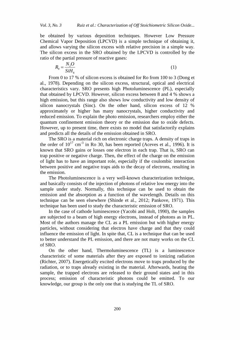
Figure 1. PL Emission of SRO with Ro 10, 20, 30 and 40, without (a) and (b)
with Thermal Treatment at 1100 °C during 3 hours in Nitrogen, all of them
Show Emission at around 420 nm, Especially as Deposited Samples. (c)
Excitation Curves of the Same Samples, the Detection Wavelength is shown in
the Legend of the Figure
400 500 600 700 800 900 10000.0
2.0k
4.0k
6.0k
8.0k
10.0k
12.0k
14.0k
16.0k
18.0k
PL
(a
.u.)
Wavelength (nm)
SRO40
SRO30
SRO20
SRO10
400 500 600 700 800 900 1000
0.0
30.0k
60.0k
90.0k
120.0k
150.0k
180.0k
210.0k
240.0k
PL
(a
.u.)
Wavelength (nm)
SRO40
SRO30
SRO20
SRO10
380 400 420 440 460 480 500 520 5400.0
2.0k
4.0k
6.0k
8.0k
10.0k
12.0k
14.0k
16.0k
18.0k
20.0k
PL (
a.u
.)
Wavelength (nm)
(a) (b)
200 220 240 260 280 300 320 340 360 380 4000.0
5.0k
10.0k
15.0k
20.0k
25.0k
30.0k
35.0k
40.0k
45.0k
50.0k
PL
(a.u
.)
Wavelength (nm)
SRO40 - 413 nm
SRO30 - 724 nm
SRO20 - 777 nm
SRO10 - 418 nm
(c)
After annealing, a relative intense luminescence band emerges around 700
nm while the luminescence around 420 nm is little affected. The strongest
increase of the red luminescence is seen in the sample with Ro 30
corresponding to a silicon excess of 5% approximately. PL emission around
700 nm increases as the R0 increases, and SRO 30 reaches the higher intensity,
after this value if the R0 is increased then the PL begins to reduce. So that, the
SRO 30 has an optimum silicon excess of 5 % approximately. These curves are
typical of SRO obtained by LPCVD, and they emit mainly in the 600 to 850
nm range. The emission is ascribed principally to SiO2 defects as oxygen
vacancies (Rodríguez et al., 2014). Defects as WOB (weak oxygen bond),
NOV (non-oxygen vacancy), E defect, NBOHC (non-bridging oxygen hole
center) and dangling bonds have been found in quartz using techniques such as
electronic spin resonance. The emissions of such defects are in the range of
415, 455, 520-560, 680-710 and 750-1100 nm (2.99, 2.73, 2.39-2.22, 1.83-
1.75, 1.66-1.13 eV) respectively, clearly in the emission range of our samples.
On the other hand, SRO 10 is rich in Sinc and it does not have so many defects,
also the silicon excess of SRO 40 (2%) is so small that the density of the
defects is not expected to be as high as that of SRO 30. Figure 1 (c), shows the
excitation curves for the different SRO films. These curves were obtained
Athens Journal of Sciences September 2016
203
fixing the detector at a specific wavelength, and then the pumping wavelength
excitation varied from 200 to 400 nm. The curves show a wide absorption
range.
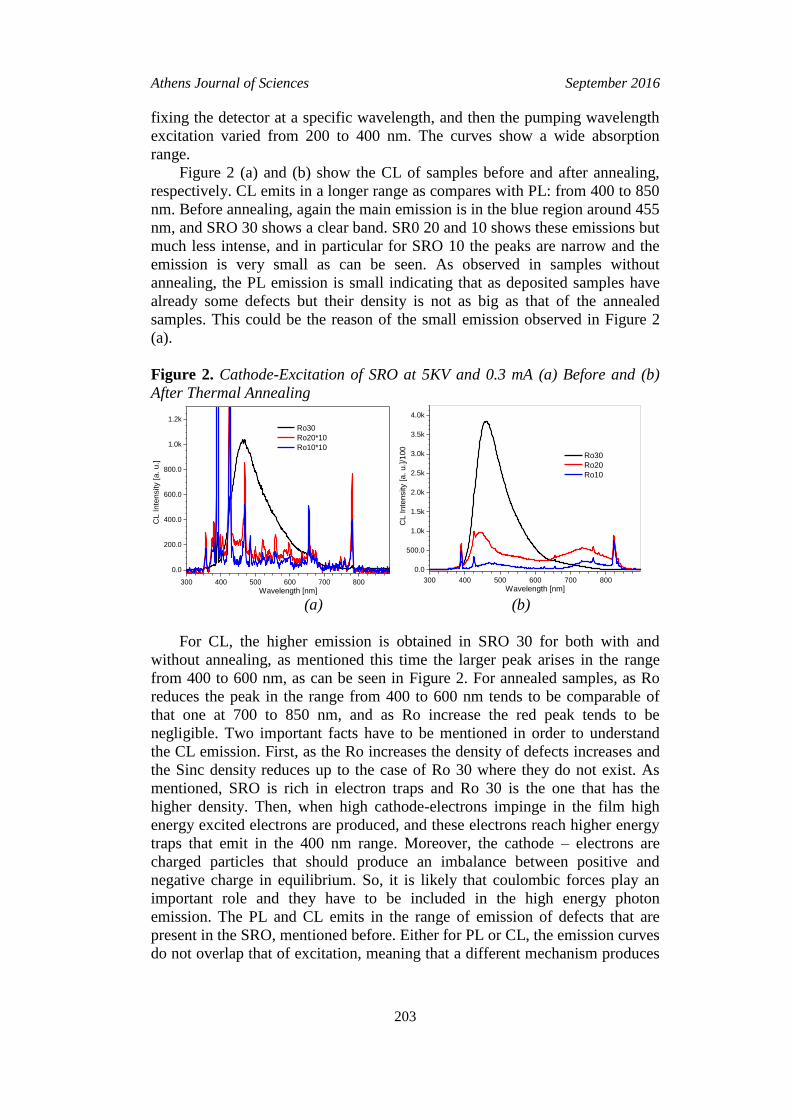
Figure 2 (a) and (b) show the CL of samples before and after annealing,
respectively. CL emits in a longer range as compares with PL: from 400 to 850
nm. Before annealing, again the main emission is in the blue region around 455
nm, and SRO 30 shows a clear band. SR0 20 and 10 shows these emissions but
much less intense, and in particular for SRO 10 the peaks are narrow and the
emission is very small as can be seen. As observed in samples without
annealing, the PL emission is small indicating that as deposited samples have
already some defects but their density is not as big as that of the annealed
samples. This could be the reason of the small emission observed in Figure 2
(a).
Figure 2. Cathode-Excitation of SRO at 5KV and 0.3 mA (a) Before and (b)
After Thermal Annealing
300 400 500 600 700 800
0.0
200.0
400.0
600.0
800.0
1.0k
1.2k
CL I
nte
nsity [a. u.]
Wavelength [nm]
Ro30
Ro20*10
Ro10*10
300 400 500 600 700 800
0.0
500.0
1.0k
1.5k
2.0k
2.5k
3.0k
3.5k
4.0k
CL Inte
nsity [a. u.]/1
00
Wavelength [nm]
Ro30
Ro20
Ro10
(a) (b)
For CL, the higher emission is obtained in SRO 30 for both with and
without annealing, as mentioned this time the larger peak arises in the range
from 400 to 600 nm, as can be seen in Figure 2. For annealed samples, as Ro
reduces the peak in the range from 400 to 600 nm tends to be comparable of
that one at 700 to 850 nm, and as Ro increase the red peak tends to be
negligible. Two important facts have to be mentioned in order to understand
the CL emission. First, as the Ro increases the density of defects increases and
the Sinc density reduces up to the case of Ro 30 where they do not exist. As
mentioned, SRO is rich in electron traps and Ro 30 is the one that has the
higher density. Then, when high cathode-electrons impinge in the film high
energy excited electrons are produced, and these electrons reach higher energy
traps that emit in the 400 nm range. Moreover, the cathode – electrons are
charged particles that should produce an imbalance between positive and
negative charge in equilibrium. So, it is likely that coulombic forces play an
important role and they have to be included in the high energy photon
emission. The PL and CL emits in the range of emission of defects that are
present in the SRO, mentioned before. Either for PL or CL, the emission curves
do not overlap that of excitation, meaning that a different mechanism produces
Vol. 3, No. 3 Ruiz et al.: Characterization of Off Stoichiometric Silicon Oxide...
204
the absorption and the emission. Nevertheless, the wide excitation spectrum
could excite all the traps in the SRO, but for PL the energy is only able to
excite mainly low energy mechanisms of emission. However, CL excites
mainly high energy centers, but it is expected that both low and high energy
centers would be excited.
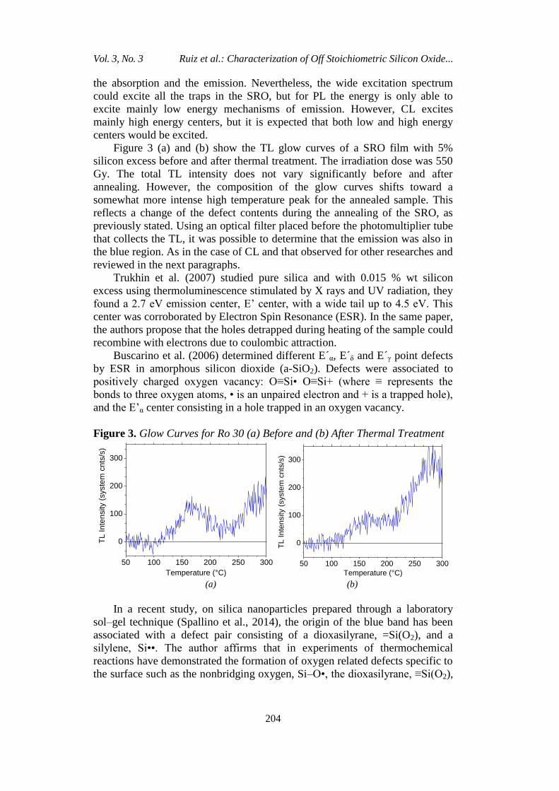
Figure 3 (a) and (b) show the TL glow curves of a SRO film with 5%
silicon excess before and after thermal treatment. The irradiation dose was 550
Gy. The total TL intensity does not vary significantly before and after
annealing. However, the composition of the glow curves shifts toward a
somewhat more intense high temperature peak for the annealed sample. This
reflects a change of the defect contents during the annealing of the SRO, as
previously stated. Using an optical filter placed before the photomultiplier tube
that collects the TL, it was possible to determine that the emission was also in
the blue region. As in the case of CL and that observed for other researches and
reviewed in the next paragraphs.
Trukhin et al. (2007) studied pure silica and with 0.015 % wt silicon
excess using thermoluminescence stimulated by X rays and UV radiation, they
found a 2.7 eV emission center, E’ center, with a wide tail up to 4.5 eV. This
center was corroborated by Electron Spin Resonance (ESR). In the same paper,
the authors propose that the holes detrapped during heating of the sample could
recombine with electrons due to coulombic attraction.
Buscarino et al. (2006) determined different E´α, E´δ and E´γ point defects
by ESR in amorphous silicon dioxide (a-SiO2). Defects were associated to
positively charged oxygen vacancy: O≡Si• O≡Si+ (where ≡ represents the
bonds to three oxygen atoms, • is an unpaired electron and + is a trapped hole),
and the E’α center consisting in a hole trapped in an oxygen vacancy.
Figure 3. Glow Curves for Ro 30 (a) Before and (b) After Thermal Treatment
50 100 150 200 250 300
0
100
200
300
TL
In
ten
sity (
syste
m c
nts
/s)
Temperature (°C)
50 100 150 200 250 300
0
100
200
300
TL
In
ten
sity (
syste
m c
nts
/s)
Temperature (°C) (a) (b)
In a recent study, on silica nanoparticles prepared through a laboratory
sol–gel technique (Spallino et al., 2014), the origin of the blue band has been
associated with a defect pair consisting of a dioxasilyrane, =Si(O2), and a
silylene, Si••. The author affirms that in experiments of thermochemical
reactions have demonstrated the formation of oxygen related defects specific to
the surface such as the nonbridging oxygen, Si–O•, the dioxasilyrane, ≡Si(O2),
Athens Journal of Sciences September 2016
205
and the silanone, Si=O. They also relate the absorption at 3.69 and 3.85 eV
(336 and 310 nm) with the emission peaks at 3.34, 3.17, 3.00 and 2.83 eV (376,
388, 414, 444 nm).
Emission at 3.2 ± 0.5 eV in the UV-Blue thermoluminescence has been
observed in SiO2 obtained by sputtering (Hickmott, 1972). In the
aforementioned report, the authors correlate the optical absorption with the
energy of a shallow trapping center. They correlate an absorption band from 2
to 8.5 eV (620 to 165 nm) with a trapping center 0.66 eV down the conduction
band for as sputtered films, and a trapping center at 0.84 eV for X ray
irradiated. They correlate these trapping centers with the 3.2 ± 0.5 eV emission
band.
From the previous discussion, it is clear that the emission of silica-based
materials has a common range of emission, and it is due to point defects that
emit in the range from 400 to 860 nm (3 to 1.45 eV). These defects have been
extensively studied and characterized. As can be observed from our results, the
SRO is not an exception and the blue to near infrared emission is observed in
films as deposited and annealed at high temperatures.
In the case of the SRO obtained by LPCVD, the high temperature during
the deposition makes the material rich in SiO2 defects from the start. These
defects are responsible for the observed PL emission in samples as deposited as
shown in Figure 1 (a). The main emission is centered at around 420 nm
coinciding with the emission reported by Spallino et al. (2014). It is then clear
that the blue emission in PL is also due to defects (Spallino et al., 2014). When
annealing takes place, a competitive process starts between the formation of
silicon clusters, and the formation and accumulation of silicon-oxide defects.
For a high percentage of silicon excess, say 12% (SRO 10), the Si clusters
dominate and the formation of Sinc is promoted instead of the defects, so low
emission intensity is expected in all wavelengths. For small Si excess, say 5%
(SRO 30), new defects should be created and accumulated causing an intense
emission in the whole range. However, for PL, the blue emission does not
increase and the red emission presents a much higher intensity. For SRO 20 the
characteristic is in between these extremes. From Figure 1 (b), it is clear that
the emission centered at around 740 is increased as Ro increases, and the SRO
30 is the optimum. For all Ro’s including SRO 10 the blue emission does not
reduce, and then the results indicate that there is no change in the defects that
produces the blue PL.
Figure 1(c) shows the excitation curves of the films. Spallino et al. (2014)
report maximums at 336 and 310 nm, and in spite of that we have blue
emission our excitation curves do not show these maximum, instead we have a
wide absorption band including the 336 and 310 nm wavelengths. The wide
excitation band shown for these films corroborates that SRO is rich in different
point defects.
Contrary to PL, the cathodoluminescence presents an intense blue
emission, especially for annealed samples. Also, as Ro increases the blue
emission increases, and the SRO 30 shows the higher emission. However, as
Ro reduces the red and the blue emission intensities tend to be comparable. The

Vol. 3, No. 3 Ruiz et al.: Characterization of Off Stoichiometric Silicon Oxide...
206
intense blue CL emission cannot be due to the same defects observed in PL,
because as stated their density is small. It is more likely that CL has to be
related to the high energetic charged carriers impinging in the films.
Figure 4 shows the PL, CL and TL in the blue range. In this figure, the blue
emission reported by Trukhin et al. (2007) is also included for comparison.
Figure 4. Normalized Spectra of CL, PL and TL of the SRO and Quartz, the TL
of Quartz was Taken from (Trukhin et al., 2007).
0.0
0.1
0.2
0.3
0.4
0.5
0.6
0.7
0.8
0.9
1.0
Inte
ns
ity
[n
orm
]
320 360 400 440 480 520 560 600 640
Wavelength [nm]
Ro30-AD-CL
Ro30-TT-CL
Quartz-TL
Ro10-AD-PL
Ro10-TT-PL
3.8 3.6 3.4 3.2 3 2.8 2.6 2.4 2.2 2
Energy [eV]
As mentioned, the fact that the blue emission occurs in deposited samples
indicates that blue emission centers are created during the growth of the film at
high temperatures by LPCVD. Also, observations of PL in the blue region for
all Ro´s indicate that the peak and the range of blue emission do not change
with the thermal treatment, as seen in Figure 1 (a) and (b) and Figure 4. It is
clear from figure 4 that two different groups of spectrum can be obtained, one
for PL and other for TL and CL shifted to low energies. Moreover, all CL and
TL spectrums are different of that of PL, meaning, again, that different
emission mechanisms have to produce them.
Another important characteristic of the SRO is charge trapping. Being the
same material the same defects that emit could act as acceptors or emitters of
electrons. For example the vacancies of oxygen can trap holes or have unpaired
electrons as discussed in the previous references. It is not difficult to think that
when photons impinge into the SRO film some electrons will acquire enough
energy to jump to another trap leaving the base state charge positive. Then, a
charge imbalance will be produced. Even more, when high-energy ionizing
radiation impinges on the films charged ions are produced. Then, high density
of electrons and positive ions result inside the SRO film. A film rich in electros
and ions will have a strong coulombic interaction. This will produce more
Athens Journal of Sciences September 2016
207
energetic photons. That is, blue emission will be more probable than the red
one.
The charge imbalance causes coulombic interaction between the charged
traps. Trying to keep the mechanism of emission as simple as possible, the
excited electrons decay between negative and positive traps due to coulombic
attractions and this will produce the emission. This model is similar to that
known as Donor Acceptor Decay, DAD (Yacobi and Holt, 1990; Richter,
2007) and is formulated as:
r
qEEEE adgPL
4
2
(2)
Where EPL is the emission energy of PL, Ed and Ea are the energies of the
acceptor and donor pair; and ε is the dielectric constant. The last term arises
from the Coulombic interaction of the carriers and depends on the pair
separation r.
In the past, our group using the DAD model proposes the distribution of
the donor and acceptor pairs in SRO (López-Estopier et al., 2011), this result
coincides with that proposed in (Spallino et al., 2014). In these references, it
was found that the intramolecular allowed energy states and the decay in these
states will produce some range of emission. That is, it has been demonstrated
that the emission is due to the point defects that have specific emissions,
however, this is not enough to explain the full range of emissions presented in
SRO by the different excitation techniques, and neither to explain the small
shifts observed.
Salh (2011a; 2011b) studied the formation of the Si-O agglomerates in
SiOx subjected to thermal annealing. He and coworkers proposed that silicon
atoms re-arrange due to heat, and could form small silicon rings given place to
a cluster of different SiOx defects. Besides, they also propose the decay of
electrons between two neighboring oxygen deficient centers. So, no matter the
type of excitation, the excited molecules emit. However, in the presence of
high density of charge, high coulombic interactions and then the decay between
molecules inside the Si-O clusters have to be promoted. The combined
emission, inside the molecules and between molecules, will produce the
observed spectrum.
Then a combined model of emission of SRO is proposed, and it is based
on the emission of the different point defects assisted by the coulombic forces.
At the moment of writing this paper we are not able to give details on the
formulation of this model, however a qualitative proposition is:
Cpd EEE (3)
Where, Epd is the point defect energy emission, and EC is the energy
associated with the coulombic interaction.
Figure 4 shows the emission of TL, CL and PL of SRO and quartz in the
blue region. As can be seen all of them are in the blue range, and their shape is
quite similar in all the cases. The blue PL, both with and without annealing, is
centered at 420 nm. So, the same point defects have to be responsible for these
emissions. Also, in PL an intense red emission is observed, due to the defect
emission. In CL the more intense emission is in the blue side and it is centered
Vol. 3, No. 3 Ruiz et al.: Characterization of Off Stoichiometric Silicon Oxide...
208
on 460 nm. The change in the wavelength intensity and the shift could be
explained due to coulombic interactions. This could be explained as follows:
when the sample is illuminated with UV light the electrons are excited by
energy enough to produce emission between states inside of the molecule as
that obtained in (Spallino et al., 2014). The low energy of the incident photons
does not produce high coulombic interactions, and so most of the emission is
due to the point defects. However, under electron bombardment of high
ionizing energy, electrons are removed from their base states and many effects
that produce charge imbalance take place promoting the emission due to
centers inside the molecules and between molecules. However, due to the high
density of the electronic charge present in films, a high imbalance between
positive and negative traps causes strong coulombic attractions. So the
electrons will have energy high enough to jump to other centers that will be
able to produce emission by coulombic attraction in different wavelengths.
Also, due to the high energy of cathode electrons, many charged particles than
contribute to the coulombic decay, will be present. The higher the density of
the traps, it is more probably that electrons reach traps in the right position to
allow radiative emission, as in the case of SRO 30. The higher the excitation of
the particles is, the higher the probability of excited electrons to decay at higher
energies is, producing high-energy emissions. This explains that CL of RO 30
after the annealing emits principally in blue with a different peak as that of PL.
After this discussion, the emission of SRO should be the sum of all of these
possibilities, as stated in Eq. 3 and illustrated in Figure 5.
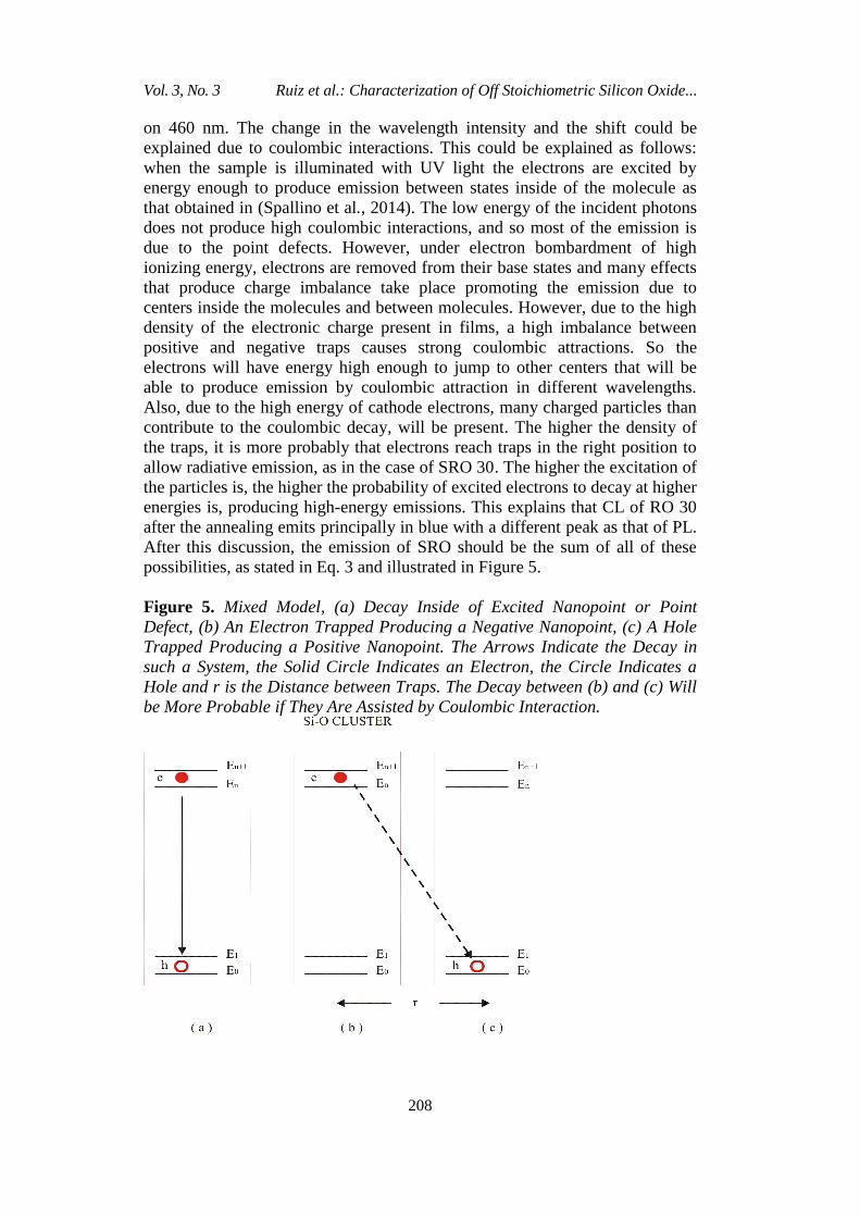
Figure 5. Mixed Model, (a) Decay Inside of Excited Nanopoint or Point
Defect, (b) An Electron Trapped Producing a Negative Nanopoint, (c) A Hole
Trapped Producing a Positive Nanopoint. The Arrows Indicate the Decay in
such a System, the Solid Circle Indicates an Electron, the Circle Indicates a
Hole and r is the Distance between Traps. The Decay between (b) and (c) Will
be More Probable if They Are Assisted by Coulombic Interaction.

Athens Journal of Sciences September 2016
209
The PL of SRO 30 after annealing could be explained with similar
arguments, but in this case because the excitation is of low energy the
coulombic component allows only for low charge imbalance. Then, the red
emission becomes dominant as seen in Figure 1(b). In the other case, high
coulombic interactions will promote the blue emission over the red one.
Conclusions
SRO films with silicon excess from 2 to 12% were studied by Photo,
Cathode, and Thermo – Luminescence. All of these techniques produce blue
emission; however depending on the charge imbalance a red or blue emission
is more probable. It is corroborated that the emission is due to silicon – oxide
defects as that observed in other material whose matrix is SiO2 and reported in
the literature. Special emphasis is paid for the blue emission that is very well
understood and reported. Absorption and emission of the nanopoints, or point
defects, has been studied and reports on the energy levels of the molecules can
be found. However, from the analysis of the different luminescent emission of
the SRO obtained by LPCVD, it is proposed that besides the intra nanopoints’
emission, coulombic interaction between positive and negative nanopoints
contributes to the emission spectrum. At the moment of writing this report, it is
not possible to establish an analytical mixed model, and more work has to be
done to obtain a model that calculates the emission spectrum of SRO obtained
by LPCVD.
References
Aceves, M., Falcony, C., Reynoso-Hernandez., A., Calleja, W. and Torres, A. (1996)
‘The Conduction Properties of The Silicon/Off-Stoichiometry-Si02 Diode’, Solid-
State Electronics Vol. 39, No. 5, 637444. doi:10.1016/0038-1101(95)00174-3.
Buscarino, G., Agnello, S., and Gelardi, F. M. (2006) ‘29 Si Hyperfine Structure of
the E’α Center in Amorphous Silicon Dioxide’. Phys. Rev. Lett. 97, 135502. doi:
http://bit.ly/1SIjgfe.
Dong, D., Irene, E. A., and Young, D. R. (1978) ‘Preparation and Some Properties of
Chemically Vapor‐Deposited Si‐Rich SiO2 and Si3 N 4 Films’. J. Electrochem.
Soc.: Solid-State Science and Technology, 125, 819-823. doi: 10.1149/1.2131555.
Hickmott, T. W. (1972) ‘Thermoluminescence and Color Centers in rf-Sputtered Si02
Films’, Journal of Applied Physics 43, 2339. doi: 10.1063/1.1661501.
López-Estopier, R., Aceves-Mijares, M., Yu, Z., and Falcony, C., (2011)
‘Determination of the energy states of the donor acceptor decay emission in
silicon rich oxide prepared by low-pressure chemical vapor deposition’, Vacuum
Science & Technology B, Vol.29, Issue 2. doi:10.1116/1.3554735.
Pankove, J. (1971) Optical Processes in Semiconductors, Dover, New York, pp. 17–
18.
Richter, D. (2007) ‘Advantages and Limitations of Thermoluminescence Dating of
Heated Flint from Paleolithic Sites’, Geoarchaeology, Vol. 22, No. 6, 671–683
(2007). doi: 10.1002/gea.20180.

Vol. 3, No. 3 Ruiz et al.: Characterization of Off Stoichiometric Silicon Oxide...
210
Rodríguez, J. A., Vásquez-Agustín, M. A., Morales-Sánchez, A., and Aceves-Mijares,
M. (2014) ‘Emission Mechanisms of Si Nanocrystals and Defects in SiO2
Materials’, Journal of Nanomaterials, 409482, http://bit.ly/1NErQHj.
Salh, R. (2011a) ‘Silicon nanocluster in silicon dioxide: Cathodoluminescence, energy
dispersive X-ray analysis, infrared spectroscopy studies’, In Crystalline Silicon -
Properties and Uses, (ed.) Sukumar Basu, Rijeka: InTech, pp. 173-218.
doi:10.5772/35404.
Salh, R. (2011b) ‘Defect related luminescence in silicon dioxide network: a review’,
In Crystalline Silicon - Properties and Uses, (ed.) Sukumar Basu, Rijeka: InTech,
pp. 135-172. doi: 10.5772/22607.
Shinde, K. N., Dhoble, S. J., Swart, H. C., and Park, K. (2012) ‘Phosphate Phosphors
for Solid-State Lighting’, Springer Series in Materials Science, Springer-Verlag
Berlin Heidelberg, pp. 41-59.
Spallino, L., Vaccaro, L., Sciortino, L., Agnello, S., Buscarino, G., Cannas, M., and
Gelardi, F. M. (2014). ‘Visible-ultraviolet vibronic emission of silica
nanoparticles’, Phys. Chem. Chem. Phys., 16, 22028-22034. doi: 10.1039/C4CP0
2995J.
Trukhin, A. N., Troks, J., Griscom, D. L. (2007), ‘Thermostimulated luminescence
and electron spin resonance in X-ray- and photon-irradiated oxygen-deficient
silica’, Journal of Non-Crystalline Solids, 1560–1566. doi:10.1016/j.jnoncrysol.
2007.01.028.
Yacobi, B. G., and Holt, D. B. (1990) Cathodoluminescence Microscopy of Inorganic
Solids, Solids Plenum, New York, 1990, pp. 43–45.


![Lecture 16 (LPCVD).ppt [호환 모드] · 2018. 1. 30. · Nano/Micro Systems & Controls Laboratory. Chemical Vapor Deposition • Polysilicon –SiH 4 → Si + 2H 2 (SiH 4 silane)](https://img.dokumen.tips/doc/110x75/611535e68b74607f95723e99/lecture-16-lpcvdppt-eeoe-2018-1-30-nanomicro-systems-controls.jpg)