Embed Size (px)
Citation preview

9-1
Chapter 9 FBs-PLC Interrupt Function
9.1 The principle and the structure of interrupt function
There are many jobs that FBs-PLC needs to carry out. For example, there are 20K words user’s program need to be solved, 512 points of I/O status need to be captured or updated, 5 communication ports need to be serviced, and etc. However, jobs can only be executed one at a time as there is merely one CPU available. Therefore, PLC service one job after another in sequence until all the jobs are executed once. Then, it will return to the first job to repeat the same cycle. The time interval of each execution is called the “scan time” of PLC. The CPU execution speed is extremely fast in comparison with human response. As far as human feeling is concerned, PLC almost completes all jobs at the same time when PLC can normally complete the foregoing huge workload within tens of milliseconds (ms). Hence, it can meet the requirements of the most practical control cases.
In most application cases, the control method described above is very much sufficient. But for some applications that require a high-speed response (such as positioning control), a delay in scan time will certainly mean an increase in error. Under the circumstances, only applying the “Interrupt” function can achieve the precision requirement.
The so-called “Interrupt” means the interrupt request to the CPU during normal scan cycle when an immediate response is required. After receiving such request, the CPU will promptly stop all scanning work to prioritize to perform and complete the corresponding service work before return (the so-called “Return from Interrupt” or RTI) to where interrupt occurred and resume the interrupted scanning work.
The service work needed to carry out while interrupt occurred is called Interrupt Service Routine, which is a subroutine consisted by a series of ladder codes. It is placed in the subroutine area and begin with the LBL instruction with reserved label name (please refer to Section 9.3). Since it is placed in the subroutine area, it will not be executed in a normal PLC scanning cycle (PLC only constantly scans the main program area but not the subroutine area).
In normal case, the CPU can promptly execute the corresponding interrupt routine within hundreds of micro-seconds when an interrupt occurred. When there are more than one interrupt occurred at the same time (e.g. FBs-PLC has 42 interrupts source), only the interrupt with highest priority can be executed. All the other interrupt routines need to wait until it became the highest priority among the pending interrupts. Consequently, a response delay of hundreds of microseconds, or even few milliseconds, may be caused. Hence, in a multiple interrupt inputs structure, an interrupt priority is given to each interrupt in accordance with its importance. In case another interrupt request is made when the PLC is carrying out the interrupt service routine for an interrupt request that has a higher priority than the new interrupt request, the CPU will wait until the execution of the subroutine is completed before accepting the new interrupt request. However, if the priority of the new interrupt request is higher than the one being executed, the CPU will stop the running of the current interrupt service routine immediately to execute the interrupt service routine with a higher priority. After completing the execution, the CPU will return to the previously interrupted service routine with a lower priority to continue the incomplete work. This kind of interrupt in an interrupt execution is called the “Nested Interrupt”. FBs-PLC can have up to 5 levels of nested interrupts. The diagram below shows the examples of single interrupts and nested interrupt:

9-2
Mian Routine Mian RoutineMian Routine
X8+ISubroutine
X8+I Subroutine
HSC0I Subroutine
First level
Second level
Nested Subroutine can have up to 5 level
X8+interrupt(Priorty:18)
HSC0 interrupt(Priority:10)
Main Routine
Subroutine
9.2 Structure and application of interrupt service routine
Although both “Interrupt” and “Call” are having subroutines, but the calling methods (to jump to subroutine for execution) are different. When the CALL command [FUN67] is executed by “Call” in the main program, the CPU will execute the subroutine with the label name designated by the CALL command. The CPU will return to the main program after the RTS (Return from Subroutine) command is executed.
The calling of “Interrupt” is triggered by, instead of using software commands, the hardware interrupt signal to the CPU. The CPU will identify the source of the interrupt and jump automatically to the “Interrupt Service Routine” with the label name of the interrupt in the subroutine for execution. It will return to the main program after the RTI (Return from Interrupt) command is executed. Therefore, there is no ladder code relevant to interrupt in the main program area.
As mentioned before, interrupt service routine must be placed in the sub program area. The structure is shown as the diagram on the right where a “head”, a “tail” and the main body of the service routine are included. The “head” is the “interrupt label name” of the interrupt (to be discussed in the next section). The “tail” is the RTI command [FUN69], to tell the CPU that the interrupt subroutine is ended and it should jump to the place where were interrupted, please refers to FUN69 (RTI) instruction. In between the “head” and the “tail” is the main body of the interrupt service routine used to tell the CPU what control actions should be executed when interrupt occurs.
RTI
Interrupt label (Head)
Main Content of interrupt service Routine
(Tail)
The power line for subroutine is indicated by double lines to differentiate from the power ine for the main program (single line) for easy reading.

9-3
9.3 Interrupt source, label and priority for FBs-PLC
As described in the last section, every “Interrupt Service Routine” should have a unique “Interrupt Label”. There are 49 corresponding “Interrupt Labels” for interrupts, namely “Interrupt Reserve Words”, cab be used in the sub program area of FBs-PLC. These labels are dedicated to the interrupt routines hence cannot use for normal subroutine or jump target.
The “Interrupt Label” (Interrupt Reserve Word) are all suffix with an “I” letter. For examples, the interrupt label for high-speed counter HSC0 should be “HSC0I” and the interrupt label for X0+ should be “X0+I”. The “Interrupt Labels” and their priorities for the 49 FBs-PLC interrupt sources of FBs-PLC are shown as below.
The following table is the interrupt sources and their label names. To compatible with previous versions of programming tool, besides HSC/HST, the label names in old versions are also enlisted (label name with parenthesis). The new label names are prefer than old while in usage (HSTAI, 1MSI~100MSI, X0+I~X15-I are prior in using).
(The priority of interrupt is inversely proportional to the value of priority)
Interrupt Source Priority Interrupt Label Condition for Interrupt Note
High Speed Timer 1 HSTAI (ATMRI) Timing from HSTA to(CV=PV)
No interrupt when act as a cyclic timer
2 1MSI (1MS) One interrupt every 1mS
3 2MSI (2MS) One interrupt every 2mS
4 3MSI (3MS) One interrupt every 3mS
5 4MSI (4MS) One interrupt every 4mS
6 5MSI (5MS) One interrupt every 5mS
7 10MSI (10MS) One interrupt every 10mS
8 50MSI (50MS) One interrupt every 50mS
Internal Time Base
9 100MSI (100MS) One interrupt every 100mS
One kind of time base interrupt is allowed at a time (please refer to Section 9.5.2). Therefore, the actual number of interrupts is 42.
10 HSC0I/HST0I Counting/Timing from HSC0/HST0 to (CV=PV)
11 HSC1I/HST1I Counting/Timing from HSC1/HST1 to (CV=PV)
12 HSC2I/HST2I Counting/Timing from HSC2/HST2 to (CV=PV)
HSC /
HST
13 HSC3I/HST3I Counting/Timing from HSC3/HST3 to (CV=PV)
HSC0~HSC3 are labeled as HSC0I~HSC3I when configured as high speed counter; and are labeled as HST0I~HST3I for high speed timer.
14 PSO0I Pulse output of PSO0 completed
15 PSO1I Pulse output of PSO1 completed
16 PSO2I Pulse output of PSO2 completed PSO
17 PSO3I Pulse output of PSO3 completed

9-4
Interrupt Source
Priority Interrupt Label Condition for Interrupt Note
18 X0+I (INT0) Interrupt when 0→1()of X0
19 X0−I (INT0−) Interrupt when 1→0()of X0
20 X1+I (INT1) Interrupt when 0→1()of X1
21 X1−I (INT1−) Interrupt when 1→0()of X1
22 X2+I (INT2) Interrupt when 0→1()of X2
23 X2−I (INT2−) Interrupt when 1→0()of X2
24 X3+I (INT3) Interrupt when 0→1()of X3
25 X3−I (INT3−) Interrupt when 1→0()of X3
26 X4+I (INT4) Interrupt when 0→1()of X4
27 X4−I (INT4−) Interrupt when 1→0()of X4
28 X5+I (INT5) Interrupt when 0→1()of X5
29 X5−I (INT5−) Interrupt when 1→0()of X5
30 X6+I (INT6) Interrupt when 0→1()of X6
31 X6−I (INT6−) Interrupt when 1→0()of X6
32 X7+I (INT7) Interrupt when 0→1()of X7
33 X7−I (INT7−) Interrupt when 1→0()of X7
34 X8+I (INT8) Interrupt when 0→1()of X8
35 X8−I (INT8−) Interrupt when 1→0()of X8
36 X9+I (INT9) Interrupt when 0→1()of X9
37 X9−I (INT9−) Interrupt when 1→0()of X9
38 X10+I (INT10) Interrupt when 0→1()of X10
39 X10−I (INT10−) Interrupt when 1→0()of X10
40 X11+I (INT11) Interrupt when 0→1()of X11
41 X11−I (INT11−) Interrupt when 1→0()of X11
42 X12+I (INT12) Interrupt when 0→1()of X12
43 X12−I (INT12−) Interrupt when 1→0()of X12
44 X13+I (INT13) Interrupt when 0→1()of X13
45 X13−I (INT13−) Interrupt when 1→0()of X13
46 X14+I (INT14) Interrupt when 0→1()of X14
47 X14−I (INT14−) Interrupt when 1→0()of X14
48 X15+I (INT15) Interrupt when 0→1()of X15
Interrupt from External
Hardware Input or Software High-Speed
Timer
49 X15−I (INT15−)
↑
HSC4I
∫
HSC7I
↓ Interrupt when 1→0()of X15
The counter input and control input of the software high speed counter HSC4 ~ HSC7 which were implemented by the interrupt function can be designated as any one input of X0~
X15. Therefore, the interrupt priority of the software high speed counter depends on the input it utilized.

9-5
9.4 How to use interrupt of FBs-PLC
The applications of interrupt in internal timing, external input, HSC/HST or PSO are similar. Since the applications of HSC/HST and PSO have been described in other chapters/sections, only examples of internal timing and external input will be described in this section.
Begin
Setup interrupt configuration ---------------Refer to section 9.5
Writing interrupt service routine in sub program area
---------------Refer to section 9.6
End
9.5 Interrupt configuration
In fact, interrupt configuration is simply to determine whether the application of a certain interrupt is to be used or not.
Interrupt configuration can be divided into configuration relevant to I/O or irrelevant to I/O two categories. HSTA, HSC/HST, PSO and external interrupt are all relevant to I/O and should be performed by the configuration function of programming tool. The programming tool will automatically enable the interrupt of the device once it is configured.
The configuration of internal time base interrupt (1MSI~100MSI), which is irrelevant to I/O, need not to be configured. As long as the time base interrupt reserved words, which is placed in front of the interrupt service subroutine, appears in the sub program area, it imply the interrupt has been planned. If more than one such interrupts appear, can use low byte, B0~B7, of the special register R4162 to control the interrupt of 1MSI~100MSI to be executed or not.

9-6
9.5.1 Interrupt configuration through the operation of WinProladder
Click the item “I/O Configuration” which in Project Windows :
Project name
System Configuration
I/O Configuration Select “Interrupt Setup”
When “Interrupt Setup” windows appear, then you can choose the Interrupt which you want.

9-7
9.5.2 Interrupt configuration through the operation of FP-07C
【Keypad Operation】 【LCD Display】
External interrupt shares the 16 high-speed input points, X0~X15, with HSC and SPD instructions. Therefore, the number of the input points used by HSC or SPD cannot configure for external interrupt.
Note: SPD instruction can only uses X0~X7 8 input points for average speed detection.
Once the interrupt configuration is determined, it cannot be changed in PLC RUN. But the EN command [FUN145] and DIS command [FUN146] provided by FBs-PLC can dynamically enable/disable the operation of interrupt of external, HSC and HSTA in PLC RUN. Please refer to the description of the two instructions.

9-8
9.5.3 Internal time base interrupt configuration by R4162
When the internal time base interrupt reserved words (8 kinds, 1MSI~100MSI) appears in the sub program area, it imply that the designated interrupt has been planned and can be masked by using the 8 bits of the low byte in the register R4162 as shown in below:
B7 B6 B5 B4 B3 B2 B1 B0
R4162: 100MS 50MS 10MS 5MS 4MS 3MS 2MS 1MS
~
~
• When bit status =0: Enable the time base interrupt (not masked) • When bit status =1: Disable the time base interrupt (masked)
Among B0~B7, if more than one of the bits is 0, FBs-PLC will enable the one with the smallest time base and disable the others. If the content of R4162 is 00H, then all time base interrupts will not be masked. However, if 1 MS and 2MS~100MS time base interrupt subroutine are all appeared in subprogram area, only the 1MS time base interrupt will be executed, and the others will not be executed.
It is with great flexibility since the user can dynamically change the time base or pause or enable the interrupt by using the ladder program to change the value of R4162 at any time in PLC RUN.
The default of R4162 is 0; it represents that 1MS~100MS time base interrupt are not been masked. As long as any one of time base interrupt processing subroutine exists in the sub program area, it will be executed periodically.
Since a considerable CPU time is required for execution of every interrupt, the smaller the interrupt time base, the more interrupts required and the longer CPU time occupied. Therefore, application should be made only when necessary to avoid degradation of CPU performance.
9.6 Examples of interrupt routine
Example 1 Precision position control by positioning switch .(Configure X0 as the positive edge interrupt input) X0 : Position Sensor X1 : Emergency Stop Y1 : Power motor

9-9
【Main program】
SET Y0M0 X0
RSTX1
Y0
• M0 (start) changes from 0→1, the motor is ON.
【Subroutine】
65LBL X0+I
EN RST Y0
EN
74.IMDI0
Y0
N :
D :
1
69RTI
• When the sensor, X0, detects the arriving of positioning location, i.e. X0 change from 0 → 1, the hardware will automatically execute the interrupt subroutine
• As motor Y0 changes to 0, it stops the motor immediately. • Output Y0 immediately to reduce delay caused by scan time
• It must employ immediate input/output instruction in the interrupt subroutine to meet the real time high speed precision control requirement.
Example 2 1MS Internal Time base Interrupt
【Main program】
ENM0
M0EN
08.MOV
D :
S :
R4162
1
R4162
S :
D :
08.MOV
0
• When M0=1, 1MS timing interrupt is disabled (1MS timing interrupt being masked)
• When M0=0, 1MS timing interrupt is enabled
【Subroutine】
65LBL 1MSI
R0(+1)EN
EN
69RTI
15
R1(-1)16
OVF
UDF
• After 1MS time base interrupt is started, the system will automatically execute the interrupt subroutine every 1MS
• R0 is used as the up counting cyclic timer for every 1MS time base
• R1 is used as the down counting cyclic timer for every 1MS time base

9-10
9.7 Capture input and digital filter In many high-speed application, you can set interrupt input to prevent signal lose. Besides, you can set Captured Input to capture the transient input signal less than one PLC scan time. The method to set Capture Input is very easy.
Click the item “I/O Configuration” which in Project Windows :
Project name
System Configuration
I/O Configuration Select “Input Setup”
When “Input Setup” windows appear, then you can choose the Capture Input point which you want.
The FBs series PLC can support up to 36 points of captured input (X0~X35) depending on the main unit. The inputs X0~X15 can be configured as the hardware interrupt input for fast response application, and the captured inputs are for low frequency but short duration (less than 1 scan time) input signal. Example_1
When the input is configured as the captured input and used for counting application, it is necessary that the input signal period must be greater than 2 scan time for correct counting. For example the input frequency is 50Hz, then the scan time of PLC must be less than 10mS for counting without loss.

9-11
Example_2
The captured input can get the input signal which duration is less than 1 sacn time of PLC.
The FBs series PLC main unit supports the captured input function as mentioned above, except this, it also supplies the digital filtering function for digital inputs X0~X35. There are 6 groups of digital inputs (X0~X3)、(X4~X7)、(X8~X11)、(X12~X15)、(X16~X23)、(X24~X35) for filtering setting.
There are 2 methods for digital filtering, one is the frequency domain, the other is the time domain. The filtering setting for upprer four groups of digital inputs (X0~X15) can be either frequency domain or time domain; while in frequency domain, it supports the range of 14KHz~1.8MHz in total 8 selections; while in time domain, it supports the range of 1~15×1mS or 1~15×0.1mS selections. The last two groups of digital inputs (X16~X35) only supports the time domain, and the selections are 1~15×1mS.
By time domain, the duration of input signal must be greater than the filtering time, then the PLC can get the input signal; by frequency domain, the frequency of input signal must be less than the filtering frequency, then the PLC can get the input signal. Example 1 When the filtering time is 2mS, if the ON or OFF duration is less than 2mS, it will lose the ON or OFF signal.
Example 2 When the filtering frequency is 28KHz, if the input frequency is greater than 28KHz, it will lose the input signal.

MEMO

10-1
Chapter 10 FBs-PLC High-Speed Counter and Timer
10.1 FBs-PLC high-speed counter
The counting frequency of an ordinary PLC’s software counter can only reach tens of Hz (depending on the scan time). If the frequency of input signal is higher than that, it is necessary to utilize high-speed counter (HSC), otherwise loss count or even out of counting may occur. There are usually two types of HSC implemented for PLC. The hardware high-speed counter (HHSC) employed special hardware circuit and the software high-speed counter (SHSC) which when counting signal changes state will interrupt CPU to performe the increment/decrement counting opeartion. FBs-PLC provides up to 4 HHSCs (in SoC chips) and 4 SHSCs. All of them are all 32-bit high speed counter.
10.1.1 Counting modes of FBs-PLC high-speed counter
As shown in the table below, each of the four FBs-PLC HHSCs and SHSCs provides 8 and 3, respectively, kind of counting modes to choose from:
Counting Waveform Counting Mode
HHSC (HSC0~HSC3)
SHSC (HSC4~HSC7) Up Counting(+1) Down Counting(−1)
MD 0 U/D U
D
Up-
dow
n pu
lse
MD 1 U/D×2 U
D
MD 2 P/R R
P
Pul
se-d
irect
ion
MD 3 P/R×2 R
P
MD 4 A/B B
A
MD 5 A/B×2 A
B
MD 6 A/B×3 A
B
AB
pha
se
MD 7 A/B×4 A
B
• The up/down arrow (↑,↓) on the positive/negative edge in the waveform represents where counting (+1 or –1) occurs.

10-2
10.2 System architecture of FBs-PLC high-speed counter
The diagrams below are the system architecture for FBs-PLC HHSC and SHSC where each one of them has multi-purpose input and counting functions. Some of the functions are built-in (such as CV register number, PV register number, interrupt label and relay number for software MASK, CLEAR and direction selection) that user need not to assign for configuration. However, some functions, with a “*” marked in the diagrams below, must use the programming tool to configure the HSC (such as HSC application selection, counting mode, application of each function input, inverse polarity and appointment of corresponding input point number Xn) etc. For detailed structure and operation of the 8 kind of counting modes that assigned in configuration, please refer to section 10.2.1~10.2.3 for explanation.
Note: CV (Current Value); PV (Preset Value).
Mask control(X2,X6,X10,X14)*
SoftwareMask
(HSC3)
(X3,X7,X11,X15)*
EN(FUN145)/DIS(FUN146)
Controllinginput
(HSC0)
(HSC1)
(HSC2)
Clear control
C *
HSC3IM1980M1979 (HSC3)
HSC0I
HSC1I
HSC2I
Interrupt MaskTO CPUInterruput
M1940 M1941
M1947
M1977
M1946
M1976
SoftwareClear
(HSC0)
(HSC1)
(HSC2)
PV=CV
CV Register (CPU Intermal Memory)
FUN92(HSCTR)
(X0,X4,X8,X12)*
(X1,X5,X9,X13)*
M1942M1948M1978M1981
Software direction selection
(HSC1)
(HSC3)(HSC2)
(HSC0)
Counting input
0:UP1:DN(MD2,3 ONLY)
M *
*
*D,R,B
U,K,A x1
* x3
x4
x2
*
(SoC Chip)
Com
parator Register
M C
Register
CV PV
PV Register(CPU Internal Memory)
FUN93(HSCTW)
(HSC0)(HSC1)(HSC2)(HSC3)
FUN93(HSCTW)
DR4104DR4108
DR4096DR4100
DR4106DR4110
DR4098DR4102
System Architecture of HHSC(HSC0~HSC3)
Use FUN92 to read out current counting value from SoC chip hardware counter to put it into CPU internal CV register.
Use FUN93 to write CV register content to SoC chip. Resets and updates the CV of hardware counter in SoC chip.
Use FUN93 to write PV register of hardware counter of SoC chip.

10-3
(CPU Internal Memory)
PV Register
(X0~X15)*
(D,R,B)*
(HSC4)(HSC5)(HSC6)(HSC7)
M1983M1985M1987M1989
0:UP1:DN(MD2 ONLY)
Countinginput
Software direction selection
M
C
Mask control
Clear control
Controllinginput
EN(FUN145)/DIS(FUN146)
M C
M1982
M1984
M1986
M1988
HSC4I
HSC5I
HSC6I
HSC7I
Software MaskInterrupt Interrupt Mask
PV=CV
CV Register
DR4112(HSC4)or
DR4116(HSC5)or
DR4120(HSC6)or
DR4124(HSC7)
(X0~X15)*
(X0~X15)*
(X0~X15)*
(HSC4)
(HSC5)
(HSC6)
(HSC7)
(HSC4)
(HSC5)
(HSC6)
(HSC7)
DR4114(HSC4)or
DR4118(HSC5)or
DR4122(HSC6)or
DR4126(HSC7)
(HSC4)
(HSC7)
*
*
*
*
Com
parator
(U,P,A)*
System Architecture of SHSC(HSC4~HSC7)
All control signals of HHSC and SHSC are default as Active High (i.e. Status =1 for active and 0 for non-active). In order to cooperate with the sensor’s polarity, the HHSC counting inputs (U, D, P, R, A and B) and control inputs (M and C) can be selected for polarity inverse.
By default when the MASK control signal, M, is 1, the HSC counting pulse will be masked without any counting being performed and all HSC internal status (such as CV and PV) will remain unchanged. The HSC will function normally only when M returns to “0”. Some sensors have Enable outputs which function is on the contrary to MASK. Counters will not count when Enable = 0 and can only start functioning when Enable = 1. Then, function of inverse polarity input of MASK can be selected to cooperate with the sensors having Enable output.
When the CLEAR control signal, C, is 1, the HSC internal CV register will be cleared to 0 and no counting will be performed. The HSC will start counting from 0 when C returns to 0. Ladder program can also directly clear the CV register (DR4112, DR4116, DR4120, and DR4124), so as to clear the current counting value to 0.
The four sets of FBs-PLC HHSC are located in the SoC chips where the CV or the PV registers the user can’t access directly. What the user can access are the CV registers (DR4096~DR4110) located in the CPU internal memory. Ideally, the contents of CV and PV registers in the chips should be updated simultaneously with the CV and PV registers in the CPU internal memory. However, to keep the correspondence between the two must be loaded or read by the CPU when they, in fact, belong to two different hardware circuits. It is necessary to use FUN93 to load the CV and the PV registers inside the CPU to the respective CV and PV registers (to allow HHSC to start counting from this initial value. Then, FUN92 can be used to read back the counting value of the HHSC CV register in the chips to the CV register in the CPU (i.e. the CV register in the CPU has the bi-direction function). Since read can only be carried out when FUN92 is executed (so-called “sampling” reading), it might result in difference between the HHSC CV value in the chips and the CV value in the CPU, the deviation will getting greater especially when the counting frequency is high.

10-4
When the counting frequency is not high or the demand for positioning precision is not so much, using FUN92 in the main program to read the current counting value and then incorporate comparator instruction is adequate for a simple counting positioning control.
When the demand for positioning precision is higher, or in the multi-zone count setting control, it may use the FUN92 to read the current counting value while in the time base interrupt routine and incorporate compare instruction to perform more precise counting positioning control.
As the demand for positioning precision is extremely high, it must use the preset interrupt function of hardware counter. The preset value can load by FUN93 into the PV register of HHSC in the chipset. When CV value of HHSC reaches this preset value, the hardware comparator in the HHSC will send interrupt to CPU at the very moment CV=PV, and jump to interrupt subroutine to do real time control or procession.
SHSC, on the other hand, uses the interrupt method to request an interrupt signal to the CPU when the counting input is on the rising edge. Then, the CPU will determine whether it should decrease or increase the internal CV register (since the CV register itself in the CPU is a SHSC CV register, no FUN92 or FUN93 is required). Each time when CV is updated, if the CPU find that it is equal to the PV register value, the CPU will jump immediately to the corresponding SHSC interrupt service routine for processing. Whenever there has a change in SHSC counting or control input can cause the CPU to be interrupted. The higher the counting frequency, the more of CPU time will be occupied. The CPU responding time will be considerably increased or even Watchdog time-out will be caused to force the PLC to stop operating. Therefore, it is preferred to use HHSC first; if it needs to use SHSC, the sum of all FBs-PLC SHSC input frequencies should not exceed 8KHz.
None of the special relay controls, such as software MASK, CLEAR and direction control, is real time. This means that although MASK, CLEAR or direction change has been set during routine scanning, the signal will only be transmitted to HSC when I/O updating is under way after the completion of routine scanning. Hence, it is not suitable for the real time control in HSC operation (which should be mainly used for initial setting before HSC operation). Should real time control be required, please use hardware to control input or apply the FUN145(EN), FUN146(DIS), FUN92(HSCTR), and FUN93(HSCTW) etc. instructions for control.
Every HSC is equipped with the functions, ENable(FUN145) and DISable(FUN146), when SHSC is disabled, it will stop counting and without the interrupt function ; when HHSC is disabled, the counting still works but the interrupt function being disabled.
10.2.1 The up/down pulse input mode of high-speed counter (MD0,MD1)
The up/down pulse input of high-speed counter has up counting pulse input (U) and down counting pulse input (D) that are independent to each other without any phase relationship. Each of them will +1 (U) or –1 (D) on the CV value when the rising edge of the pulse input occurs (both positive and negative edge for MD1). This also applies when the rising (or falling) edge of the U and D pulse occur simultaneously (it will offset with each other). Both of the two modes have the built-in software MASK and CLEAR (CLEAR is not available for SHSC) control functions, when the control function are not in use should keep the status (such as M1940 and M1941) as “0”. Apart from the built-in software MASK and CLEAR, the controls of hardware MASK and CLEAR can also be configured. The MASK control is first performed by the OR operation of the hardware and software control, then the result is send to the HSC MASK control M, and so does CLEAR. Taking HSC0 as an example, the function schematic diagrams for MD0 and MD1 configured separately are shown as below.

10-5
HSC0
CV PVU
D
M C
x1
EN/DIS EN(FUN145)/DIS(FUN146)
M1940 M1941
Up pulse X0 HSC0I InterruptDown pulse X1
Hardware mask X2
Hardware clear X3
Software mask Software clear
Down pulse X1
Hardware mask X2
Hardware clear X3
Software mask
Up pulse X0PVCV
Software clear
HSC0I Interrupt
EN(FUN145)/DIS(FUN146)
M1940 M1941
D
M
Ux2
EN/DISC
HSC0
MD0(U/D) MD1(U/D×2)(HHSC Only)
The Waveforms of the HSC, which is configured as up/down pulse input mode, and PV value is preset to 6:
X0(U)
X1(D)
M1940 or X2 (M)
M1941 or X3 (C)
PV=6
CV (x1)
HSC0I
MD0
CV (x2)
HSC0IMD1
01
23
43
23
45
6
0
12
34
56
76
54
56
78
910
1112
HSC0 sends interrupt to CPU CPU receives and handles this interrupt
HSC0 sends interrupt to CPU

10-6
10.2.2 Pulse/direction input mode of high-speed counter (MD2, MD3)
The pulse-direction input mode high-speed counter only has one counting pulse input P (pulse). It requires another direction input R (Direction) to decide whether the CV value should +1 (R=0) or –1 (R=1) when the rising edge (both rising and falling edges for MD3) of counting pulse arrives. The same applies to counting of MD2 and MD3 except that MD2 only counts on the rising edge (+1 or –1) and MD3 counts on both rising and falling edges of PS pulse (twice the counts of MD2). These two modes have built-in software MASK, software CLEAR (SHSC does not have clear). When control function is not in use, it must keep the status (such as M1946 and M1947 in this example) to be 0. Apart from the built-in software MASK and CLEAR, the controls of hardware MASK and CLEAR can also be configured. The MASK control is first performed by the OR operation of the hardware and software control, then the result is send to the HSC MASK control M, and so does CLEAR. The function schematic diagrams of HSC1 configured individually for MD2 and MD3 are shown as below.
HSC1
Pulse input X4Direction selecrion X5
CV PVP
R
M C
x1
EN/DIS
Hardware mask X6
Hardware clear X7
Software mask
HSC1I Interrupt
EN(FUN145)/DIS(FUN146)
Software clearM1946 M1947
HSC1
CV PVP
R
M C
x2
EN/DIS EN(FUN145)/DIS(FUN146)
Software direction selection M1948
M1946 M1947
M1948
Pulse input X4
Hardware mask X6
Hardware clear X7
Software mask
HSC1I Interrupt
Software clear
Software direction selection
Direction selection X5
MD2(P/R) MD3(P/R×2)(HHSC Only)
Direction selection of MD2 and MD3 HSC, for HSC or SHSC, can be come from the external inputs (such as X5 in this example) or the special relay in CPU (such as M1948 in this example) to reduce the usage of external input points.

10-7
The diagram below is the waveform diagram for the relationship between counting and control of the two HSC. In this example the PV value is to 6.
CV (x1)
HSC1I
MD2
CV (x2)
HSC1IMD3
HSC1 sends interrupt to CPU
HSC1 sends interrupt to CPU CPU receives and handles this interrupt
X5(DIR)
X6(M)
X7(C)
PV=6
12
34 4
5 5 56
78
98
76 6
78
910
1112
12
34 4
5 5
34
67
0
X4(PS)
10.2.3 AB phase input mode of high-speed counter (MD4,MD5,MD6,MD7)
The AB phase high-speed counter is equipped with phase A and phase B pulse input with counting value +1 or –1, depending on the phase relationship between the two, i.e. the related counting of the two phases. If phase A is ahead of phase B, the CV value should be +1, else, the CV value should be –1. The counting of the four modes, MD4 (A/B), MD5 (A/B×2), MD6 (A/B×3) and MD7 (A/B×4), of AB phase HSC are similar. Their differences are:
MD4 (A/B) : The rising edge of A is +1 when A is ahead of B and the falling edge of A is –1 when A is behind B.
MD5 (A/B×2) : The rising and falling edges of A are +1 when A is ahead of B, and –1 when A is behind B (twice the counts of MD4).
MD6 (A/B×3) : The rising and falling edges of A and rising edge of B are +1 when A is ahead of B. The rising and falling edges of A and the falling edge of B are –1 when A is behind B (three times the counts of MD4).
MD7 (A/B×4) : The rising and falling edges of A and B are +1 when A is ahead of B and the rising and falling edges of A and B are –1 when A is behind B (four times the counts of MD4).
10-8
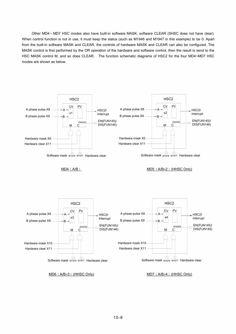
Other MD4~MD7 HSC modes also have built-in software MASK, software CLEAR (SHSC does not have clear). When control function is not in use, it must keep the status (such as M1946 and M1947 in this example) to be 0. Apart from the built-in software MASK and CLEAR, the controls of hardware MASK and CLEAR can also be configured. The MASK control is first performed by the OR operation of the hardware and software control, then the result is send to the HSC MASK control M, and so does CLEAR. The function schematic diagrams of HSC2 for the four MD4~MD7 HSC modes are shown as below.
HSC2
CV PVA
B
M C
x1
EN/DIS EN(FUN145)/DIS(FUN146)
M1976 M1977
B phase pulse X9
A phase pulse X8
Hardware mask X0
Hardeare clear X11
Hardware clearSoftware mask
HSC2I Interrupt
A phase pulse X8
B phase pulse X9
Software mask
Hardware mask X0
Hardeare clear X11
PVCVHSC2I Interrupt
Hardware clear
EN(FUN145)/DIS(FUN146)
M1976 M1977
B
M
Ax2
EN/DISC
HSC2
MD4(A/B) MD5(A/B×2)(HHSC Only)
HSC2
CV PVA
B
M C
x3
EN/DIS EN(FUN145)/DIS(FUN146)
M1976 M1977Software mask
Hardeare clear X11
Hardware clear
B phase pulse X9
A phase pulse X8 HSC2I Interrupt
Hardware mask X10
A phase pulse X8
B phase pulse X9
Hardware mask X10
Hardeare clear X11
Software mask
PVCVHSC2I Interrupt
Hardware clear
EN(FUN145)/DIS(FUN146)
M1976 M1977
B
M
Ax4
EN/DISC
HSC2
MD6(A/B×3)(HHSC Only) MD7(A/B×4)(HHSC Only)

10-9
The diagram below is the waveform diagram for the relationship between counting and control of the four HSC modes in this example when the PV value is set as at -4.
tsr u vqp
o
mn
wx
y
efg
hi
jk
l
Retruct point
Rotary encoder
X8(A)
Down counting(B phase ahead A phase)
Up counting(A phase ahead B phase)
X9(B)
X10(M)
X11(C)
CV(x1)
PV=-4
HSC2I
MD4
CV(x2)
PV=-4
HSC2I
MD5
MD6:CV(x3)
MD7:CV(x4)
o p q r s
1 23 4
s
0
3 21 0
r q p o n m
0
l k j i h g
-1 -2-3 -4
-5
CPU receives and handles this interruptHSC2 sends interrupt to CPU
00
0 0
0 0
-1 -2 -3 -4 -5
112 23 34 45 6
7 8 7 6 5
-6-7 -8 -9
-10
CPU receives and handles this interruptHSC2 sends interrupt to CPU
123456
1 2 3
6
9 9
12
-1-2 -3
-6
-9
-12
-1513
56
9
1212
9
6
321
15
-1-3
-6
-9
-12
-20
0
Retract point

10-10
10.3 Procedure for FBs-PLC high-speed counter application
Start
Configure HSC counting mode and respective input
(by FP-07C or WinProladder) -------------
1. Please refer to Section 10.2 for respective HSC counting modes and principles.
2. Please refer to Section 10.4 for setting examples.
Complete hardware wiring according to the previous input assignment
-------------1. Please refer to “Digital Input Circuit” in Chapter 6 “Hardware Manual”
for hardware wiring.
Set HSC initial CV value and interrupt PV value in the main program
-------------
1. If the HSC is HHSC, it is necessary to apply FUN93 to load it into the HHSC CV and PV in the SoC chip.
2. Please refer to Section 10.5 for program examples.
Write necessary handling procedures to be taken during interrupt and condition for next interrupt in sub program area
-------------
1. Please refer to Section 9.1 for subroutine structure. 2. Please refer to Section 10.5 “Actual Examples” for program
examples.
Start the operation -------------. Please refer to Section 10.5 for program examples and description.
End
10.4 HSC/HST configuration
10.4.1 HSC/HST configuration (Using WinProladder)
Click the item “I/O Configuration” which in Project Windows :
Project name
System Configuration
I/O Configuration Select “Timer/Counter”
When “Timer/Counter” window appear then you can choose the Timer or Counter which you want.

10-11
---《Timer/Counter Configuration》---
【 Counter Type 】: It can select Hardware Counter or Hardware Timer.
【 Counting Mode 】: It can select the Counting Mode( Example: U/D、P/R、A/B……)
【 A-Phase 】: Select the up pulse input signal. If the Mode is P/R Counting Mode ,and this item will be “PS”; If the Mode is U/D Counting Mode ,and this item will be “Up”.
【 B-Phase 】: Select the down pulse input signal. If the Mode is P/R Counting Mode ,and this item will be “DIR”; If the Mode is U/D Counting Mode ,and this item will be “Dn”.
【 Mask[MSK] 】: It can select Mask input.
【 Clear[CLR] 】: It can select Clear input.
---《HSC Polarity》area ---
【 Mask signal 】: Determining Mask signal is positive or negative.
【 Clear signal 】: Determining Clear signal is positive or negative.
【 Counter signal 】: Determining Counter signal is positive or negative.
---《HSC’s Data Length》area ---
It can choose 32-bit Hardware Counter mode or 16-bit Timer + 16-bit Counter mode. 32-bit Hardware Counter mode means using two register to record the Counting value. The 16-bit Timer + 16-bit Counter mode means using one register to record Counting value and the other register will be cyclic Timer.

10-12
10.4.2 HSC/HST configuration (Using FP-07C)
The screen of FP-07C will be taken as an example to describe HSC Configuration in this section. The HSC Configuration, in sequence, includes the following 5 items:
Select assignment for HSC/HST (only HHSC provides this item selection function). Proceed to next item if selection is HSC. No other items are required if configured as HST.
Assign respective HSC counting modes (MD0~MD7). After keying in the mode number, FP-07 will automatically display the HSC counting and control input names of the mode and reserve space for users to key in the external input point number Xn. The blank mode field indicates the HSC is not in use.
Determine whether the respective counting inputs (U, D, P, R, A and B) and control inputs (M and C) are to be applied or not (reserve the space if not in use and fill in the Xn value if it is to be applied. As respective Xn input values of HHSC are fixed, it requires only to key in alphabet “X” and FP-07C will automatically make up the preset number n).
Select whether the polarity of each HHSC counting input (U, D, P, R, A and B) is inverse or not, so as to match the polarity of the encoder (0: Not inverse, 1: Inverse. Preset as 0).
Select whether the polarity of each HHSC control input (M and C) is inverse or not, so as to match the polarity of the encoder (0: Not inverse, 1: Inverse. Preset as 0).

10-13
Examples applying FP-07C to perform the above mentioned ~ configurations
【Key Operation】 【LCD Display】
a
b
HSC0 is preset as HSC
HSC1 is preset as HSC
HSC1 is used as a high-speed counter HST1
HSC2 is preset as HSC
HSC3 is preset as HSC
MD field is blank indicating that HSC0 is not in use
There is no need to configured HSC1 as it has been set to HST (No Display).
MD field of HSC2 is blank indicating MD is not in use
* After 7 is keyed in, the respective MD7 input names will be displayed and the preset values for A and B (X8 and X9) will be filled automatically
If MASK is required, just key in X and it will automatically fills number 10
C

10-14
【Key Operation】 【LCD Display】
*
b
Key in 2 and the preset number of P will be filled automatically
Move the cursor to R and key in “X”, it will immediately change to X13 and change it to be hardware direction control
HSC4 is not in use
HSC5 is not in use
HSC6 is set as MD0 and respective input names of MD0 SHSC will be displayed automatically
Assign X10 as the up counting pulse “U” for HSC6
Assign X2 as the down counting pulse “D” for HSC6
HSC7 is not in use
All counting inputs of every HHSC(HSC0~HSC3)are preset as non-inverse
All MASK controls of HHSC are preset as non-inverse
Change all MASK inputs of HHSC to inverse (i.e. the MASK function becomes ENable)
All CLEAR controls of HHSC are preset as non-inverse
Complete configuration and return to the initial screen display (HSC0/HST0 Item Selection)
Input value modification can be made by directly key in the new value to overwrite. Use key to delete any input value, if required.
A blank field (without any value input) indicates the application of the HSC or the input is not required.
“pulse” in the previous example represents the “Counting Input”, i.e. U and D, P and R or A and B, of HHSC.
“POLAR” represents “POLARITY”, i.e. selection of inverse or non-inverse.
C

10-15
The input point for respective HHSC counting and control inputs are fixed. Therefore, in the “Configuration Examples” of the previous example, it needs only to key in “X” for each HHSC input to indicate that the input is to be applied and FP-07C or WinProladder will automatically make up the preset number for X, to which no change will be allowed. The user may assign respective SHSC counting or control inputs between X0~X15 freely. Hence, it is necessary to key in both the “X” and the number n for SHSC input point number to make it complete.
All preset or selectable input point numbers, software MASK, software CLEAR, direction selection and other related numbers of HHSC and SHSC are summarized in the table below:
MC/MN MA
HHSC SHSC SHSC
Type
Signal Allowed HSC0 HSC1 HSC2 HSC3 HSC4 HSC5 HSC6 HSC7 HSC4 ~ HSC7
CV Register DR4096 DR4100 DR4104 DR4108 DR4112 DR4116 DR4120 DR4124 The same as SHSC of MC/MN
PV Register DR4098 DR4102 DR4106 DR4110 DR4114 DR4118 DR4122 DR4126 The same as SHSC of MC/MN
U,P or A
X0 X1/X4 X4/X5/X8 X5/X12 X0~X15 X0~X15 X0~X15 X0~X15 The same as SHSC of MC/MN Counting
Input D,R o r B
X1 X5 X9 X13 X0~X15* X0~X15* X0~X15* X0~X15* The same as SHSC of MC/MN
Mask X2 X6 X10 X14 X0~X15 X0~X15 X0~X15 X0~X15 The same as SHSC of MC/MN Control
Input Clear X3 X7 X11 X15 X0~X15 X0~X15 X0~X15 X0~X15 The same as SHSC of
MC/MN
Software MASK Relay
M1940 M1946 M1976 M1979 M1982 M1984 M1986 M1988 The same as SHSC of MC/MN
Software CLEAR Relay
M1941 M1947 M1977 M1980 Clear the Current Value Register directly
Software Direction Selection(MD2,3 Only)
M1942 M1948 M1978 M1981 M1983 M1985 M1987 M1989 The same as SHSC of MC/MN
Interrupt Subroutine Label
HSC0I HSC1I HSC2I HSC3I HSC4I HSC5I HSC6I HSC7I The same as SHSC of MC/MN
* When SHSC works in MD2(P/R), direction chose by special relay M1983、M1985、M1987 and M1989.
When working in A-B Mode(HHSC as MD4~MD7、SHSC as MD4), whose A/B input must be used in pair, as X8 and X9.(even number is A-Phase and odd number is B-Phase)
The input point of X0~X15 in the table above can only be assigned once (i.e. used as one function), which can’t repeat to be used.
FBs-MN’s frequency can reach up to 920 KHz.( single phase and AB phase)
FBs-MC’s frequency can reach up to 120 KHz. ( single phase and AB phase)
The total input frequencies of SHSC can’t be exceed 8 KHz; the higher the frequency, the more it occupy the system (CPU) time, and the scanning duration will be extended abruptly.
MA only support SHSC.

10-16
10.5 Examples for application of high-speed counter
Example 1 This example uses high-speed counter for equal-length cutting control.
Mechanism
HSC configuration (Just set HSC0 to MD7 and complete the configuration)

10-17
Control program
【Main Program】
EN
EN
EN
T0
Y1
Y0
X4
X4
X4
Y1RST
10.01ST0
X2
TUP
Y0
R0
HSC0
PVHSC0
S :
D :CN:
HSCTR92
CV
0HSC0
S :CN:D :
EN
EN
93DP.HSCTW
93DP.HSCTW
• Use FUN 93 to write the contents of the current value register into the CV register of HSC0 in the SoC chip CN =0 indicates HSC0 D =0 indicates CV
• Use FUN 92 to read the counting value of the HSC0 CV register in the SoC chip (store into DR4096)
• Store the counting of cutting length DR0 into DR4098 and use FUN93 to store the value into the PV register of HSC0 in the SoC chip CN =0 indicates HSC0 D =1 indicates PV
• Start the motor
• Turn the cutter Y1 ON for 0.1 second
【Subroutine】
11D .(+ )
74 .IM D I0
LB L
U /S
E N
E N
R 0S b :R 4098D :
B R
C Y
R 4098S a :
N :D :
1Y 1
D =0
H S C 0IY 1
65
69R T I
93D .H S C TW
C N :D :
E N S :H S C 0
P V
R 4098
• When HSC0 CV=PV in the SoC chip, the hardware will automatically execute the interrupt subroutine labeled HSC0I
• When counting is up, turn Y1 ON (to cut materials)
• Output Y1 immediately to reduce the error caused by scan time
• Calculate new cutting position and load HSC0 PV
【Description】
1. The main program will initialize the HSC0 CV (CV=0) in advance and move the cropping length (DR0) to the HSC0 PV before starts Y0 to turn on the motor for material conveying.
2. When CV reaches PV, the length of R0 is added to the PV before being reloaded into HSC0 PV.
3. When all materials are rolled out, the material shortage detector X2 will be ON and stop the motor.

10-18
Example 2 Example of high speed counting up action processed by Interrupt
【Main Program】
M100
M101
M100
PVD :
92
93DP.HSCTW
HSC0
HSC0
S :CN:
EN
PSET
HSCTR
EN
EN
R0
Y0
HSC0
93DP.HSCTW
S :ENCN:D :
0
CV
• Employ FUN93 to write the content of current value register into the CV of HSC0 in SoC chip (reset) CN =0, represents HSC0 D =0, represents CV
• Employ FUN92 to read out the current counting value of HSC0 in SoC chip, and store it into the CV register (DR4096) CN=0, represents HSC0
• As M101 change from 0→1, start Y0 ON (begin to operate)
• Employ FUN93 to write the content of preset register into HSC0 PV in SoC chip, which serves as setting value of counting up interrupt CN=0, represents HSC0 D =1, represents PV
【Subroutine】
RTI69
65
74.IMDI0
EN D :N :
EN RST
LBL
Y01
Y0
HSC0I
• Hardware high speed counter #0 interrupt label
• When time up, it sets Y0 OFF (stop)
• Let Y0 out immediately, so as to stop promptly (otherwise Y0 will have a scan time output delay)

10-19
Example 3 Example of Immediate response of multi-zone high speed counting up by Interrupt Processing
【Main program】
M101
X3
N : 8
SET
D :
D :N :
Y8
Y8
8Y8 ERR
RST M110
HSC1R200
CN:D :
S :
PV
R100
HSC1EN HSCTR
RST
92
1/0
EN
EN
EN
EN
EN
ENP
P
P
93DP.HSCTW
114P.Z-WR
74P.IMDI0
• Employ FUN92 to read out the current value of HSC1 in SoC chip, and store it into current value register DR4100 CN =1, represents HSC1
• As M101 change from 0→1, clears the pointer register to 0
• Clears the flag of the last zone to be OFF
• Employ FUN93 to write preset register content into HSC1 PV in SoC chip, which serve as counting up setting value. CN =1, represents HSC1 D =1, represents PV
• Clear Y8~Y15 to be OFF
• Set Y8 ON, it represents that it is at the zone 0 currently
• Set Y8~Y15 output t immediately

10-20
【Subroutine】
RTI69
RST
66
D :
JMP
41.BITWR
15(+1)
N :D :41.BITWR
N :
Ts :
Pr :L :
S :
Rd :
93D.HSCTW
D :
N :D :
74.IMDI0
CN:
101D.T R
LBL
EN
65
CLR
EN
INC
EN
INB
INB
EN
EN
M110
M110EN
EN
EN
HSC1
110
Y88
PV
R4102
R4102
R100
R2008
ERR
END
R100
R100WY8
R100
ERR
OVF
110
WY8
Y15
ERR
X3+I
93D.HSCTW
D :CN:
RTI
HSC1I
S :EN
69
65LBL
LBL65
0HSC1
CV
M110
• Label name for the X3 rising edge interrupt service subroutine of X3+1 (it must assign X3 to be the rising edge interrupt input)
• When X3 changes from 0→1,employ FUN93 to write the current register content to the HSC1 CV in SoC chip (reset).
CN = 1, represents HSC1 D = 1, represents CV
• Labeled as HSC1I hardware high speed counter interrupt service subroutine.
• Turn Y15 OFF when the last zone finished.
• Make the previous zone output OFF
• Set the pointer point to the next zone
• Set the output of next zone to be ON
• Move the counting value of next zone (beginning from DR200 pointer pointed register) to the preset register DR4102
• When it’s the last zone, the M110 is ON
• Employ the FUN93 to write the preset value into the HSC1 PV in the SoC chip, which serves as counting up interrupt setting point. CN =1, represents HSC1 D =1, represents PV
• Y8~Y15 output transmitting immediately

10-21
10.6 FBs-PLC high-speed timer
The minimum timing unit (time base) of an ordinary PLC can only reach 1ms, on which the deviation in scan time should also be added. Therefore, it is necessary to apply high-speed timer (HST) if a more precise timing (e.g. using timer to cooperate with HSC for frequency measurement) is required.
FBs-PLC is built in a high-speed timer (HSTA) with a time base of 16-bits/0.1mS and, as described previously, four 32-bit high-speed counters (HSC0~HSC3) of HHSC that can work as the high speed timer (HST0~HST3) with a time base of 32-bit/0.1mS for using. Thus, FBs-PLC can have up to five high-speed timers. As HSC and INT, all HST can be enabled or disabled (default as enable) by the instructions EN (FUN145) and DIS (FUN146). HSTA and HST0~HST3 are respectively described as below.
The finest time base for most of the ordinary PLC is 10mS. Though some PLC may have HST with a time base of 1mS. When deviations in the PLC scan time is taken into consideration (e.g. if the scan time is 10ms when the time base is 1mS, the total deviation still exceeds 10mS), the figure of 1ms becomes meaningless. Therefore, these PLCs can’t be applied in high precision timing. FBs-PLC, having a time base of 0.1mS, has no deviation in scan time for its time up is sent out by interrupt to provide a precision 100 times better than ordinary PLCs’ timer application and can be used for many applications demanding precision timing.
10.6.1 HSTA high-speed timer
HSTA is a 16-bit hardware timer built in the SoC chip. As HHSC, it must use the instruction FUN93 (HSCTW) to load the PV to the HSTA PV in the chip, and with the instruction FUN92 (HSCTR) to read for CV. HSTA can be used as
a timer having two different functions. FBs-PLC will use it as a general 16-bit delay timer when PV ≥2 and as a 32-bit cyclic timer when PV=0.

10-22
A. HSTA 16-bit high-speed delay timer (Timely interrupt timer)
After HSTA starts timing, the delay timer will delay for a time of PVx0.1ms before sending an interrupt out. When PV>0, HSTA served as a delay timer which is 16-bit and its PV value can be set as 0002H~FFFFH. i.e. the delay time can be set as 0.2mS~6.5535 seconds. Except that having a more precise time base and being able to send an interrupt out immediately at time-up to provide a much higher timing precision, the applications of HSTA are the same as an ordinary delay timer. The diagram below is the structure diagram for HSTA being used as a delay timer. Please refer to Section 10.6.3 “Program Examples” for detailed function and application.
PV=CV
R4152 R4154(HSTA)CV Register PV Register
FUN92(HSCTR)
16 bit 16 bit
CV PVUP
0.1mS time base
EN(FUN145)/DIS(FUN146)
Com
parator
Interrupt labelHSTAI
EN/DISEN/DIS
FUN93(HSCTW)(SoC Chip)
EN(FUN145)
DIS(FUN146)
PV
CV(R4152)
HSTAI
Td=0.1ms x PV Td1 Td2 Td=Td1 + Td2
Timing/Non-timing
Non-timing
Apply FUN93 to write the PV into preset register of HSTA high speed timer in SoC chip, which serves as timely interrupt timer (for every set point of timer it perform once the timely interrupt subroutine with label name of “HSTAI”).
PV 2≧

10-23
B. HSTA 32-bit high-speed cyclic timer
The so-called “Cyclic Timer” is a timer that add 1 to its current value for every fixed interval and will persistently carry out up counting cyclic timing. Its CV value will cycle around as 0, 1, 2, … 2147483647, 2147483648, 2147483649, …… 4294967295, 0, 1, 2, … (as the time base is 0.1ms, CV value x 0.1ms will be its accumulative time). In fact, the cyclic timer is an up counting cyclic timing clock having a time base of 0.1ms that can operate endlessly and be used to read any two events at the time when they occurred and to calculate the time interval between the occurrence of the said two events. The Diagram B as shown below is the structure diagram for HSTA being used as a 32-bit cyclic timer. As shown in diagram, when cyclic timer PV=0, it will not send out the interrupt. To obtain the timing value, it is necessary to use FUN92 to access the CV value from the SoC chip and save it to the 32-bit CV register (DR4152) in the PLC. The typical application of the cyclic timer is for more precision of turning speed (RPM) detection under the circumstances when the change in turning speed (RPM) is huge or when it is extremely low. Please refer to Example of Section 10.6.3 for description.
DR4152 R4154(HSTA)
FUN92(HSCTR)
16 bit 16 bit
CV PVUP
0.1ms Time base
EN(FUN145)/DIS(FUN146)
EN/DIS
FUN93(HSCTW)(SoC Chip)
2147483647
0.1mS
0 1 2147483649214748364824294967295 4294967295 0
Employ FUN92 to read out the CV of HSTA high speed counter in SoC chip and store it into CV register (DR4152) so as to let the user know the value for time lapsed.
Employ FUN93 to write the PV=0 to HSTA high speed timer set point register to make it serve as 32-bit cyclic timer.

10-24
10.6.2 HST0~HST3 high-speed delay timer
A. HST0~HST3 high-speed delay timer (Timely interrupt timer)
HHSC (HSC0~HSC3) can be configured as four 32-bit high-speed delay timers, HST0~HST3. They have the same functions and time base as a 16-bit HSTA delay timer except that HST0~HST3 are 32-bit to plan HHSC as HST only needs to select “1” in the HSC/HST Item Selection under Item 8 “HSC/HST/INT” of FP-07C or WinProladder “Configuration”. Please refer to the example (to configure HSC1 as HST1) in Section 11.4 “HSC/HST Configuration”. The diagram below is the function structure diagram for HHSC being planned as a HST. Its applications are the same as that of a 16-bit HSTA. Please refer to Section 11.6.4 “Program Examples”.
DR4108 DR4110(HST3)
CV Register(CPU Internal Memory)
PV Register(CPU Internal Memory)
FUN92(HSCTR)
CV PVUP
0.1ms time base
EN(FUN145)/DIS(FUN146)
Com
parator
TO CPUInterrupt
EN/DISEN/DIS
DR4106DR4102DR4098
DR4104 (HST2)DR4100 (HST1)DR4096 (HST0)
(HST0)
(HST3)
(HST3)(HST2)(HST1)(HST0)
HST3IHST2IHST1IHST0I
Interrupt label
FUN93(HSCTW)
FUN93(HSCTW)
(SoC Chip)
B. HST0~HST3 32-bit cyclic timer
According to demand, configured the HHSC(HSC0~HSC3) to be the 32-bit timers of HST0~HST3. For interval of every 0.1ms, the current timing value register in SoC chip will be increased by 1. User may use FUN92 instruction to read out the current timing value and store it into the CV registers (DR4096, DR4100, DR4104, and DR4108) of CPU. Therefore the content of CV register of CPU become 0, 1, 2, ……, 7FFFFFFFH, 80000000H, ……., FFFFFFFFH, 0, 1, …… etc. variation of values for 32-bit. With the timing calculation technique to count the interval between two events, it can obtain infinite number of 0.1ms 32-bit timers.
Apply FUN93 to write the PV into the SoC chip which is served as set point for timing up interrupt.
Employ FUN92 to read out the current timing value in SoC chip and store it into the CV register of CPU. So as to let user know the current timing value.
It may also employ FUN93 to write the CV into the SoC chip so as to reset the timing value.
Interrupt label

10-25
10.6.3 Examples for application of high-speed timer HSTA
Example 1 HSTA serve as 32-bit cyclic timer
M1EN
M10S :
92HSCTR HSTA
D :CN:
PVHSTA
EN
93DP.HSCTW
• Employ FUN93 to write the preset value into the HSTA PV in the SoCchip CN =4, represents HSTA D =1, represents PV
• Employ FUN 92 to read out the current timing value of HSTA in SoC chip and store it to DR4152 (DR4152 value change from 0,1,2, ……,FFFFFFFF,0,1,2,……cyclic variation, the unit is 0.1mS)
• CN =4, represents HSTA
Example 2 Application example for cyclic timer
This example uses HSTA as a cyclic timer, cooperating with HSC0, to read the time interval for accumulation of 10 pulses and sending an interrupt out each time as 10 pulses are accumulated and, reciprocally, find out the required RPM (the number of pulses is fixed when the time varies).
Mechanism
HSTA
HSC0
FUN92
UX0
INT
PLCMotor
(Y0 motor driving)(X1 starting switch)
Light chopper(1 pulse/revolution)
HSC and HST configuration
As HSTA is built in, no configuration is required. Simply make PV =0 to make it as a 32-bit cyclic timer.
To cooperate with the photo interrupter, set the HSC0 as an up counting counter having single input (MD0, but use only U input).
※ All other settings (polarity of counting and control inputs) are preset (non-inverse) and should not be changed.

10-26
【Main Program】
1JMPEN
U/S
ENR4Sb :
D : R6
Sa :
12D.(-)
R2
BR
CY
D=0
EN
M1
X1
M1924EN
EN
HSCTR HSTA
R2D :
66
08D.MOV
S : R4152
Y0
CN: HSTA
92
D : PV
93D.HSCTW
S : 0
EN
EN
M19240S :
93D.HSCTW
CN:D :
S :HSC0
PV
10
D :CN:
CVHSC0
93D.HSCTW
D=0Sa : 6000000EN
65LBL 1
U/S D :Sb :
M1
R6ERR
14D.( )
R100
• Employ FUN93 to write current value 0 into the CV of HSC0 in SoC chip (reset) CN =0, represents HSC0 D =0, represents CV
• Write 10 into the preset register in SoC chip, which acts as interrupt value for counting up; FUN93 CN=0 indicates HSC0 and D=1 indicates PV
• Write 0 into the preset register, and HSTA is configured as a
32-bit high-speed cyclic timer FUN93 CN=4 indicates HSTA and D=1 indicates PV
• Read the current timing value
• The initial value of HSTA CV register is stored to DR2
• Find interval for each HSC0 interrupt
• RPM 60T
N speed Rotating ×
∆=
N=10, S10000previousCVcurrentCV
=ms1.0×CV=T)( -
∆∆
Therefore RPM CV
6000000 speed rotating
∆=
• R100=RPM
• Clear the calculation flag of RPM

10-27
【Subroutine】
RTI
93D.HSCTW
69
ENHSC0CN:
D : CV
S : 0
M1
08D.MOV
HSC0I
08D.MOV
HSCTR92
EN
EN
EN
65LBL
R4152S :D : R2
D :S :
R4R2
HSTA
• Each time when HSC0 accumulates 10 pulses, the hardware will automatically run this interrupt subroutine
• Read the HSTA CV
• Reset the current value to 0
• M1=ON, RPM calculating flag
X0
HSC0I
∆T =
8 9 10 1 10 1 9 10 1
10 10 10 10 10 10
=1200RPM =10RPM
HSC0CV value
PV value
10000(1s)
V value of HSTA1ms time basc)
15000(1.5s)
200000(20s)
800000(80s)
DT = 0.5s DT = 60s
NRPM= x60 ∆T
NRPM= x60 ∆T
RPM=RPM=
CV value of HSTA (0.1mS time base)

10-28
Example 3 HSTA serve as timely interrupt timer program
【Main Program】
M05
PVHSTACN:
D :
S :
93DP.HSCTW
EN
• Set up the period of timely interrupt time. PV=5 represents that it performs the interrupt service subroutine with the label name of HSTAI every 0.5mS.
• Employ FUN93 to write the preset value into HSTA PV in SoC chip, which serve as time up for interrupt preset value.CN =4, represents HSTA D =1, represents PV
【Subroutine】
74.IMDI0
RTI
N :
69
EN D : Y01
17D.CMP
HSTAI
HSCTR92
U/S
EN
EN
65LBL
R4096Sb :Sa :
R0a>b
a<bY0
a=b
HSC0
• Interrupt service subroutine with the label name of HSTA.
• Read the current value of hardware high speed counter HSC0 once every 0.5mS.
• To tell whether the current counting value is greater than or equal to R0. if yes, then Y0 will be ON.
• Update output Y0 immediately, so as to reach the high speed output reaction (otherwise there will be introduced a delay in scan time)

10-29
10.6.4 Examples for application of high-speed timer HST0~HST3
HSC and HST configuration(Using WinProladder)
Click the item “I/O Configuration” which in Project Windows :
Project name
System Configuration
I/O Configuration Select “Timer/Counter”
When “Timer/Counter” windows appear, then you can choose the “Hardware Timer” in Counter Type item, then HHSC (Hardware High Speed Counter) can configure to be HHT.(Hardware High speed Timer)
User don’t have to configure the HSTA, because the HSTA is default. Only you want HHSC(Hardware High Speed Counter) to be HHT.(Hardware High speed Timer) and you have to configure it.
HSC and HST configuration(Using FP-07C)
• HSC0 is set as HST0
• HSC1 is preset as HSC
• HSC1 is set as MD0, an up counting counter with single input. Other inputs will not be used.
• All other settings (polarity of counting and control inputs) are default (Non-inverse) and should not be changed.

10-30
Example1 Application example for delay timer
This example configures HSC0 as a HST0 delay timer. At the same time, by connecting the high-speed counter HSC1 with a rotary motor of an automatic wood drilling machine and sending out an interrupt at a fixed period. Each time interrupt occur will read the counting value of the counter. Then, by comparing the change in speed between the number of the motor’s rotation when no loading is applied (operating without drilling) and that when the drill head is pressing down (drilling), the change of the motor’s RPM can be calculated. It is understood that resistance will be less and motor’s RPM will be faster when the drill head is normal (sharp) than when the drill head is blunt. When the drill head is broken, it works like operating without drilling that no resistance exists and RPM is the fastest. Usually the difference in rotating speed among the three conditions is not significant and which cannot be sampled and detected by an ordinary timer having a more than tens of ms of deviation. However, applied with an HST having a time base of 0.1ms that incorporating interrupt, the drill head’s status (normal, blunt or broken) can be detected and, thus, warning can be given or operation can be stopped in due time for drill head replacement.【The time is fixed and the number of pulses varies】
Mechanism
HST0
HSC1
FUN92
UX4
INT
PLCMotor
(Y0 motor driving)(X1 starting switch)
Light chopper(8 pulses/revolution)
【Main Program】
Y 8D :
0S :E N
E N
E N
T 0
X 1
5 0 0T 0 T U P
3
R 0R 1 0 0
1 1 2 .B K C M P
R s :
L :T s :
E R R
H S T 0C V
.0 1 S
C N :D :
Y 0
E N
E N
M 1 9 2 4
9 3 D .H S C T W
H S T 05 0
9 3 D .H S C T W
P VD :C N :S :
C VH S C 1
0
9 3 D .H S C T W
C N :D :
S :
• Employ FUN93 to reset current value register in SoC chip. FUN93 CN=1 indicates HSC1 and D=0 indicates CV
• HST0 PV value is set as 50, i.e. one interrupt every 5ms (50×0.1ms)
• The initial value of HST0 CV register is 0
• Use FUN112 to compare the drill head’s RPM speed after starting the motor for 5 seconds R0: The number of HSC1 pulses obtained in every 5ms

10-31
【Subroutine】
R T I
6 9
D :C N :
P VH S T 0
1 1 D .(+ )
9 3 D .H S C T W
0 8 D .M O V
E N
U /S
E N
E N
5 0S b :
R 4 0 9 8S :
R 4 0 9 8D :
B R
C Y
R 4 0 9 8S a :
R 4 1 0 0D :S :
R 2
D = 0
H S T 0 I
1 2 D .( - )
H S C T R9 2
U /S
E N
E N
6 5L B L
R 4 1 0 0S b :D :
S a :R 2R 0
B R
C Y
D = 0
H S C 1
• The hardware will execute this subroutine once every 5ms
• Read the current counting value of HSC1 and put it into DR4100
• Find out the increment of HSC1 CV value in this 5ms interval and store the value into DR0
• Calculate the new HSC0 PV
【Description】
Supposed that the drill head’s normal RPM is 18000rpm and the photo interrupter will generate 8 pulses in one revolution, then the frequency of the pin U of HSC1 is 18000/60×8=2400Hz, i.e. 12 pulses will be generated for every 5ms. Therefore, HST0 can be used to send an interrupt and read the HSC1 CV value every 5ms to get the RPM value.

10-32
X4
HST0I
∆T DT = 5mS(50 x 0.1mS)
DT = 5mS(50 x 0.1mS)
DT = 5mS(50 x 0.1mS)
∆CV=12(24 - 12)
∆CV=12(36 - 24)
∆CV=12(47 - 36)
11 12 13 23 24 25 35 36 37 46 47 48
50 100 150 200
50 100 150 200
HSC1CV value
HSC0CV value
HST0PV value
(0.1mS time base)
HSC1 increased value
Upper Limit Lower Limit
R101 R100 ←→ → Y8
R103 R102 ←→ → Y9
R105 R104 ←→
R0 (CV)
→ Y10
※ Setting different upper and lower limits to category the RPM condition
Example2 Hardware high speed timer HST3 serve as 32-bit cyclic timer
M300
M300
HSCTREN92
D :
HST3
CV
S :CN:
0HST3
93DP.HSCTW
EN
• As M300 change from 0→1, clear the current value register to 0
• Employ FUN 93 to write current value 0 into the HST3 CV (reset) in SoC chip CN =3, represents HST3 D =0, represents CV
• Employ FUN92 to read out the current timing value of HST3 in SoC chip and store it into the current value register DR4108 (DR4108 value cyclically changes from 0, 1, 2, ……, FFFFFFFF, 0, 1, 2, …… the unit is 0.1mS) CN =3, represents HST3

10-33
Example3 Hardware high speed timer HST3 serve as periodic interrupt timer
【Main Program】
M1924
M300
M301
EN145P
EN HST3I
146P
93DP.HSCTW
ENCN:D :
S :
D :
HST3PV
5
CV
93DP.HSCTW
EN S :CN:
EN DIS
0HST3
HST3I
• Turn on or M301 is ON, it prohibits the HST3 from sending periodic interrupt
• As M300 change from 0→1, clear the current register to 0
• Employ FUN93 to write current value 0 into the HST3 CV (reset) in SoC chip. CN =3, represents HST3; D=0, represents CV
• Set up periodic interrupt interval; PV=5 represent every 0.5mS perform once the interrupt service subroutine with label name of HST3I.
• Employ FUN93 to write the preset value into the HST3 PV in SoC chip, which serve as time up interrupt preset value. CN=3 represents HST3; D =1 represents PV
• Enable the HST3 interrupt
【Subroutine】
R TI
S :C N :D :
69
ENHST3
C V
0
93D .H SC TW
N :
74.IM D I0
D :
R s :Ts :
112.BKC M P
D :L :
HST3I
92H SC TR
EN
EN
65LBL
EN
Y88
R10008
Y8
R 4096 ER R
H SC 0
• Hardware high speed Interrupt service subroutine with the label name of HST3I.
• Read the current value of hardware high speed counter HSC0 once every 0.5mS.
• To tell which zone of the electronic drum does the current counting value fall, and set the corresponding output point to be ON.
• Update output Y8~Y15 immediately
• Employ FUN93 to reset current value register into the HST3 CV in SoC chip (reset). CN=3 represents HST3; D=0, represents CV

MEMO

11-1
Chapter 11 Communication of FBs-PLC
The FBs-PLC main unit has been built in the communication port0 with optional USB or RS232 interface. If additional communication boards (CB) have been purchased, then it can increase to 2~3 communication interfaces (depending on the model of CB). If it is still not enough, communication modules can be added to expand the number of communication interfaces to 5 (PORT0~PORT4). There are three types of communication interfaces, RS232、RS485 or Ethernet, to choose from in both CB and CM. Among them, Port 0 is a permanent interface for FATEK communications interface, which is controlled by the CPU of the PLC, using FATEK “Standard communication driver” to manage the communication transactions of the Port, i.e. “FATEK communication protocol”. Any access to the Port must comply with the format of “FATEK communication protocol” to get responses from the PLC. This includes starting character, station no., command code, body, error check code, ending characters, etc.; for more details please refer to “Appendix 2: FATEK communication protocol”. WinProladder and numerous HMI and SCADA softwares are equipped with communication drivers complying with this communication protocol, therefore where the parameters on hardware interface and communications are consistent, communication connection can be established by just connecting the communication Port with the “Standard Interface”. If the communication driver with complying communication protocol is not available, besides writing its own commands complying with “FATEK communication protocol” to communicate with PLC, the commonly used industrial ModBus RTU protocol can also be used to establish a connection with FBs-PLC. The factory setting and the PLC system initialization on Port 1 ~ Port 4 default to FATEK standard communication interface; though in order to meet the extensive application and requirements of communication connection, Port 1 ~ Port 4 provides FATEK standard communication interface, as well as providing easy communication commands that support powerful functions to allow users to compile their required communication application software through the Ladder diagram program, and easily achieve the aim of system integration and distributed monitoring. Further detail will be explained in subsequent chapters.
11.1 Functions and applications of FBs-PLC communication ports
Besides the hardware interface distinction of USB, RS232,RS485 or Ethernet among the 5 COM ports of FBs-PLC, there are also 3 software interface types in terms of software interfaces. The table below shows the software interface types that can be configured on the 5 COM ports of FBs-PLC:
Communication Port Available types Software Interface Port0 Port1 Port2 Port4 Port5
Notes
Standard Interface
Port controlled by CPU, using FATEK ”Standard communication driver” or ModBus RTU communication driver, but Port0 does not support ModBus RTU communication protocol.
Dedicated Modem interface
Port controlled by CPU, using the Modem driver + FATEK ”Standard communication driver” or ModBus RTU communication driver.
Ladder diagram program controlled interface
Port controlled by users (Ladder diagramprogram )
Interface type configuration method -
Register configure
PLC Auto configure
PLC Auto configure
PLC Auto configure
• Standard Interface : Port0 ~ Port4 can all be configured into this type of interface (Port0 can only be this type of interface and only provides FATEK standard communication driver). Under this interface type, the Port is controlled by the standard communication driver of FBs-PLC (using FATEK communication protocol or ModBus RTU communication protocol), hence called “standard interface”. To communication with the “Standard Interface”, the connection can only be established by complying with FATEK FB-PLC communication protocol or ModBus RTU communication protocol.
※ Port0 doesn’t support ModBus RTU communication protocol.

11-2
• Dedicated Modem Interface : Only Port1 can select this interface type. Under this interface type, Port1 is controlled by the built-in “MODEM driver” of FBs-PLC, in charge of telephone reception or dialing tasks, and then hand the connection over to FATEK standard communication driver after the connection is established, subsequent operation is the same as the “Standard interface” above.
• Ladder diagram Program controlled interface : Port1 ~ Port4 can all select this interface type. Under this interface type, the Port will be controlled by the user’s Ladder diagram program instructions, such as FUN94, FUN150, FUN151, etc., hence users can gain control of the Port through the Ladder program.
The following sections will detail the functions and applications of the 5 Ports on FBs-PLC under each of the 3 different software interfaces.
* Port0 ~ Port4 communication parameter are default to :
Baud Rate: 9600 bps Data Length: 7 Bits Parity: Even Stop Bit: 1 Bit
11.1.1 Communication port 0 : USB or RS232 interface
Functional specification
• USB interface complies with standard functional specification of USB1.1
• RS232 interface functional specification complies with the EIA RS232 standard, with 5 types of communication speeds 9600, 19200, 38400, 57600 and 115200 configurable.
Basic usage
• Besides providing the standard RS232 interface, models with USB interface are also provided since more and more notebook computers are using USB port to replace COM ports due to light weight and thickness considerations.
• The main purpose of Port0 is to provide a communication interface for program editing, so generally speaking it would be in passive receiving mode.
Extended usage
Besides program editing, it can also connect to HMI, SCADA equipped with FATEK communication driver.
Through conversion of interface signal into RS485 signal, connections can be made with RS485 interface peripherals, such as computers, WinProladder, HMI, SCADA, etc. or become a Slave of the FATEK CPU Link network.
11.1.2 Communication port1~port4 : RS232 or RS485 interface
Functional specification
• RS232 interface functional specification complies with the EIA RS232C standard, communication parameters are adjustable up to highest communication rate of 921.6Kbps. Factory setting and system initialization communication parameter is configured to the default communication parameter.
• RS485 interface functional specification complies with EIA RS485 standard.

11-3
Basic usage
There are 3 types of software interface are selectable as follows : Standard interface : Connectable to peripherals with RS232 or RS485 interface, such as computer, WinProladder, HMI, SCADA, etc.
Port1 dedicated modem interface : It can actively or passively connect to remote computers or conduct auto information gathering, warning, anomaly reporting or dial B.B. call for remote servicing via MODEM.
Ladder diagram Program controlled interface : User can control Port1~Port4 through the ladder diagram instructions, such as FUN94 (ASCWR) command to take control of Port1 and connect to printers with RS232 hardware interface for Chinese/English report printing; FUN151 (CLINK) command takes control of Port1~Port4 to establish connection with FATEK CPU Link or peripherals with RS232 or RS485 interfaces; FUN150 (MBUS) command can turn Port1~Port4 into a master of ModBus RTU communication protocol for connecting Slaves with this communication protocol.
Port2 can provide FATEK high speed CPU Link function.
Extended usage
• Under Standard interface, act as the Slave for multi-drop FATEK RS485 or point to point RS232 CPU LINK network.
• Under Ladder diagram program controlled interface types, Port1~Port4 has the following functions:
Use MD0 mode of FUN151 (CLINK) instruction to act as the master for FATEK CPU Link network.
Use MD1 mode of FUN151 (CLINK) instruction to actively connect to intelligent peripherals equipped with this communication interface, such as other brands’ PLC, servo driver, temperature controller, inverter, message display, etc.
Use MD2 mode of FUN151 (CLINK) instruction for connection to receive the intelligent peripherals equipped with this communication interface, such as card readers, bar code readers, weighing scales, etc.
Port2 can utilize MD3 mode of FUN151 (CLINK) instruction to act as the master for FATEK high speed CPU Link network.
Use FUN150 (MBus) instruction to act as the Master for ModBus RTU communication protocol to connect to peripherals with this communication protocol.
11.1.3 Ethernet interface
Functional specification
• Comply with IEEE802.3 standard to provide 10Base T interface.
Basic usage
• Provide intranet or internet connectivity within the plant. It can connect to WinProladder, HMI, SCADA with Ethernet network interface and FATEK communications driver or ModBus driver.

11-4
Extended usage
• It can coordinate with MD0 mode of FUN151(CLINK) instruction to provide remote data acquisition through the Ethernet network between the PLC’s. ( ﹡Client Mode).
Note : For details on Client Mode of FBs-PLC network interface, please refer to the explanations in section 11.8.5.2.
11.2 How to use FBs-PLC communication functions
Refer to the diagram in Section 2.2 “Combination of PLC and Peripheral Systems” in the “Hardware Manual” for the connection of FBs-PLC to the host computer, intelligent peripherals, and other PLCs.
Among Port0~Port4, only Port 2 provides real-time response function (real-time: data is processed immediately when received or sent without being affected by scan time.) and communicates with binary code (two times ASCII code). Other ports use ASCII code for communication in the standard mode and data will not be processed until the scan is complete and housekeeping is active. Thus, there will have the service delay because of the scan time. Port2 should be provided for each PLC to share data with each other via “FATEK high-speed CPU Link” (i.e., the MD3 mode of FUN151 (CLINK) ) to meet the real time monitor requirements. Port0, Port1, Port3, Port4 should be used for intelligent peripherals, HMI, SCADA, and other non-real-time control applications for data collection and monitoring.
11.3 Hardware wiring notifications for RS485 interface
In the FBs-PLC communication interfaces, RS232 provides only point to point connection function while RS485 provides connection for multiple stations. Its wiring distance should conform to the restriction specified in the EIA standard.
The principle that connection distance should be as short as possible and the station should be far away from high noise sources must be observed for hardware wiring. RS232 is for point to point connection with a shorter connection distance and the standard cable sold in the market or provided by FATEK is applicable. However, for high-speed RS485 network, communication quality is affected and operation might be seriously interfered with if the problems, such as high baud rate, long connection distance, high signal attenuation, multiple stations, bad grounding, high noise, terminating impedance mapping, and topology, are not solved appropriately. Please read the notes of hardware wiring for RS485 network at the end of this section carefully. Limits on the number of stations
Though the number of FBs-PLC stations can be set up to 254, 16 stations are the maximum for hardware driving for RS485 interface. If more than 16 stations are required, a RS485 amplifier (FBs-CM5R) must be used. 16 additional stations can be assigned to one amplifier up to the max. 254 stations.
FBS-PLC
#1 #2
Max. 16 stationof PLC
FBS-PLC FBS-PLC FBS-PLC FBS-PLC FBS-PLC FBS-PLC
FBS-CM5R FBS-CM5R
Max. 16 stationof PLC
#16 #17 #18 #32
Max. 254 station of PLC
RS485 RS485 RS485
#254

11-5
Limit on distance
The following diagram shows the relationship between the baud rate and transmission distance of RS485 standard interface.
10K
4K
1K
100
40
4040 100K 1M 10M
Baud Rate (bps)
()feet
Transmission D
istance
Cable
Use the shielded twisted pair cables for connection. Cable quality is an important factor to transmission signal. When the baud rate is high, low quality twisted pair (e.g., PVC twisted pair cables) will cause extremely high signal attenuation and considerably shorten the transmission distance. Its noise immunity is poorer. In a circumstance where the baud rate and noise is high, and the distance is long, use high quality twisted pair cables (such as Belden 9841 polyethylene twisted pair cables), Its dielectric loss can be 1000 times lesser than that of PVC twisted pair cable. But in a circumstance where the baud rate and noise are low, PVC twisted pair cable is an acceptable and economical alternative. If the transmission distance is too long to raise signal attenuation, use a RS485 amplifier (FBs-CM5R) to amplify signal.
Topology
Topology is a graph structure of transmission connection. The topology of RS485 must be in a Bus structure. All cables must be connected from the first station to the second station, from the second station to the third station, …… to the last station. As shown in the following diagrams, both star and ring connections are not allowed. If FBs-CM5H is used, RS485 can be set to star connection, but ring connection is still not allowed.
RS485D D D D D DF F FG_+G_+ G_+RS485 RS485
the shorterthe better
the shorterthe better
BUS connection

11-6
D+
FBS-CM5H
GND2
CH2+
GND4
CH4+
CH3+ CH3-
G_+
RS485
DD FG_+G_+
RS485 RS485
D D F FD D
FG
GND3
RS-485網路搭配FBS-CM5H即可配成星狀連結
RS485D D F_+ G
FG GND1
CH1+24+
IN 24-
CH1-
F
RS485D D+ _ G
RS485FG
D D+ _
G_+ G_+
RS485 RS485
D D F
FG
CH4-
FD DG_+
RS485
DD F
CH2- FG
D+
RS485D F_ G
RS485G_D F
FG
RS485D D+ _
RS485
GD D F_+
D+
D+
D+
環狀連接(不允許)
F G
RS485
_+D
D
星狀連接(不允許)RS485G+
D D_ F
D F_ RS485G
G
RS485
F
D +D _
D FRS485_ G
G RS485D_ FG+ RS485D_D F
Ring connection
Star connection
RS485 network can collocate with FBs-CM5H to be Star connection

11-7
FG grounding
Though RS485 network can be connected with two cables, the connection is easily affected by noise. To improve communication quality, the ground potential difference (common mode voltage) between two stations should not exceed the max. allowable common mode voltage of the R485 transmission IC. 7V shall not be exceeded when FBs-PLC IC is used; otherwise, RS485 may not operate normally.
D D FG_+
D D FG_+
Ecom 7VPlace A Place B
No matter how the ground potential is, we recommend using a twisted pair cable covered with shielding. The FG of each station is connected with the ground wire covered with shielding (similar to the above-mentioned ”topology”) to clear common mode voltage and provides the shortest circuit for signal transmission to improve the anti-noise capacity.
Terminating impedance
Different transmission cables have different characteristic impedance (the characteristic impedance of a twisted pair cable is approximately 120Ω). When the signal is transmitted to the terminating resistor of a cable, reflection and waveform distortion (either sinking or protruding) will be caused if the terminating impedance is different from its characteristic impedance. This distortion is not obvious when the cable is short but it will be more serious with longer cables. Finally, PLCs cannot transmit correctly and a terminating resistor should be installed to solve this problem. A 120Ω terminating resistor has been installed inside the FBs-PLC. When a terminating resistor is required to be added, open the cover and toggle the DIP switch to the “ON” position (DIP switch is set to “OFF” position by the factory). Terminating resistors can only be added to each PLC on the utmost left and right ends of the Bus. All the DIP switches between both end should be on the position “OFF”, or the driving power of RS485 may become insufficient. The diagram below shows the setting and application of terminating resistors:
SW
DD+
F
SW
DD+
F
SW
DD+
F
SW
DD+
F
NT ON
12
NT ON
12
NT ON
12
NT ON
12
(The end of left
station)
(The end of right station)
Should open PLC's cover, adjust to "ON" for most left and right PLC units.
adjust to "OFF"
Should open the cover, adjust to “ON” for most left and right PLC units.

11-8
Strategies against noise
When wiring for RS485 network is implemented based on the described materials and rules or a 120Ω terminating resistor is added, most noise situations are eliminated. However, if noise cannot be eliminated, it means that there are strong noise sources near the RS485 network. Besides keeping cables far away from noise sources (e.g., electromagnetic valves, inverters, servo drivers, or other power units), the most effective way to solve the problem is to use noise suppression components. Refer to the description in Section 7.5 in the “Hardware Manual” for noise suppression of electromagnetic valves, relays and other devices with inductive load. The diagram below shows the noise suppression approaches for inverters, servo drivers, and other high-noise power units (i.e., add X capacitance or Y capacitance or X+Y capacitance).
C
C
C
CC
C
R S T W R S T W
C
C
C C C
C
R S T
R
S
T
W
(Add X capacitor)
(Add Y capacitor)
(Add X+Y capacitor)
C = 0.22µf~0.47µf/AC630V
Caution
• Hardware wiring for communication network and addition and removal of communication stations should be implemented with PLC disconnected. Don’t work especially when PLC is running, or communication errors may occur to generate incorrect PLC output.
11.4 How to use FBs-PLC communication ports
The requirements for communication are that (1) hardware interfaces and mechanisms, (2) communication parameters and (3) software interfaces (i.e. the protocol) of the receiver/ sender must be consistent. The same are applicable to PLC. After the above three fundamentals are meet, PLC will communicate with other PLCs or peripherals. The following will describe these three fundamentals.
11.4.1 Matching of hardware interfaces and mechanisms
In order to meet the interface requirement of variety peripherals, the FBs-PLC provides USB, RS232, RS485 and Ethernet communication interfaces for choice. When install, care should be taken if the hardware interface is of the same type. Incorrect connection of different type of communication interface may cause the permanent hardware failure. Also please make sure that the signals of mating connector are all match. For example, TXD must connect to RXD, RTS (if any) should be connected to CTS. The interface of USB, RS232 and RS485 are described at bellow (Ethernet is described at section 1.8).

11-9
Port0 USB interface (built in)
The FBs-PLC equipped with port0 USB interface can be order by suffixed an U letter in the CPU model number. The port0 can only be acted as slave. Its connector is a standard USB B type connector. The user can use the standard USB A to USB B cable (can buy from FATEK, the product number is FBs-USBP0-180, please refer the description at below) to connect the PC and PLC.
Port0 RS232 interface (built in)
The CPU model number with no U letter suffixed is a FBs-PLC that built in a port0 RS232 interface. The connector for port0 RS232 is a 4 pin Mini-DIN female connector. FATEK provides a dedicated connection cable that has a 9 Pin D-sub female connector at one end for the PC or peripherals to connect PLC port0 RS232. The wiring diagrams of port0 USB and RS232 connection cable are shown at below.
FBs-232P0-9F-150 (Mini-DIN male 9 Pin D-sub female) :
GND
+5V
RXD 1234
9876
54321
TXD
Female Mini-DIN(PLC Side)
Male
FBs-232P0-9M-400 (Mini-DIN male 9 Pin D-sub male) :
GND
+5V
RXD 1234
9876
54321
TXD
Male Mini-DIN(PLC Side)
Male
Model Description
FBs-232P0-9F-150 Dedicated for FBs RS232 Port 0 to 9Pin D-sub female, 150cm long.
FBs-232P0-9M-400 Dedicated for FBs RS232 Port0 to 9Pin D-sub male, 400cm long.
FBs-USBP0-180 Port0 USB cable (standard commercial USB A B), 180cm long.

11-10
F B s − 2 3 2 P 0 − 9 F − 1 5 0
(connector specification) (connection distance) unit/cm F: Female M: Male 9: 9Pin D-sub
P0:Port0 (RS232) P0:Port0 (USB) 232:RS232
FBs-Series product
name
USB:USB1.1 Port1~Port4 RS232 interface (expandable)
The communication port of Port1~Port4 can be utilized by installed the RS232 communication board (or module). Each communication board (or module) provides one or two standard RS232 9 Pin D-sub female connector(s). While application, the user can buy a standard 9 pin RS232 cable directly from computer store or follow the example diagram at below to DIY the cable.
Signal Name Pin
Connector Type TXD RXD RTS CTS SG DTR DSR
MALE 3 2 7 8 5 4 6 9Pin D-sub FEMALE 2 3 8 7 5 6 4
port1、port2 usage only FBs PLC Non-usage
9P D-sub female 9P D-sub male RS232 communication cable :
9876
54321
9876
54321
MaleFemale
( )
( )Port on the PLC
External Interface

11-11
9P D-sub male 9P D-sub male RS232 communication cable :
9876
54321
9876
54321
MaleMale
If you make RS232 cables by yourself and the definition of each pin is not clear, use a multimeter for measurement to determine TXD and RXD.
9 Pin connector: The pin 5 is SG; Measure the pin 2 (red probe) and the pin 5 (black probe) with a multimeter. If it is approximately −9V, it means that the pin 2 is the transmission pin; If it is approximately 0V, it means that the pin 2 is the receiving pin. Measure the pin 3 (red probe) and the pin 5 (black probe) by a multimeter. If it is approximately −9V, it means that the pin 3 is the transmission pin; If it is approximately 0V, it means that the pin 3 is the receiveing pin.
Port1~Port4 RS485 interface (expandable)
The communication port of Port1~Port4 can be utilized by installed the RS485 communication board (or module). Each communication board (or module) provides one or two standard RS485 3-pin European plug-able terminal block. The pin assignment of connector(s) is show below.
+ (D+)
G (FG)
(D )
11.4.2 Selection and setting of communication protocols
Besides offering the FATEK protocol by default, Port1~Port4 can be set to ModBus (Slave) protocol. The following shows the setting steps in the WinProladder :
Click the protocol: PLC
Setting
Protocol a port can be set to ModBus RTU or FATEK Protocol:

11-12
Besides, you also can setting the communication protocol through special register.
R4047 : Upper Byte = 55H, configure the communication port for ModBus RTU protocol. = Other values, Port1~4 don’t support ModBus RTU protocol(The defaults are FATEK protocol) Lower Byte : Port assignment for ModBus RTU protocol.
Format as below :
Upper Byte Lower Byte 55H b7 b6 b5 b4 b3 b2 b1 b0
b0, Reserved ; b1=0, Port 1 acts as FATEK protocol. =1, Port 1 acts as ModBus RTU protocol. b2=0, Port 2 acts as FATEK protocol. =1, Port 2 acts as ModBus RTU protocol. b3=0, Port 3 acts as FATEK protocol. =1, Port 3 acts as ModBus RTU protocol. b4=0, Port 4 acts as FATEK protocol. =1, Port 4 acts as ModBus RTU protocol.
b5~b7, Reserved ※ It allows to assign multiple ports for ModBus RTU protocol, where the corresponding bit must be 1. For example : R4047=5502H, Assign Port 1 as ModBus RTU protocol; R4047=5504H, Assign Port 2 as ModBus RTU protocol; R4047=5506H, Assign both Port 1 and Port 2 as ModBus RTU protocol;
Refer to : The rule for address mapping between ModBus and Fatek(Page12-40).

11-13
11.4.3 Settings for communication parameters
Communication parameters can be set up for each of the 5 FBs-PLC ports. When out of factory or communication parameters of Port 0~Port 4 are set to the same parameters of Port 0 before shipment or after system initialization. (See the table below.)
Baud Rate 9600 bps
Data Length 7 Bits
Parity Check Even
Stop Bit 1 Bit
Default communication parameters
Port Register
Setup Default Value Default Baud Rate Other default Parameters
Port 0 R4050 5621H 9600 bps 7-bit Data, Even、1-bit Stop Port 1 R4146 5621H 9600 bps 7-bit Data, Even、1-bit Stop Port 2 R4158 5621H 9600 bps 7-bit Data, Even、1-bit Stop Port 2
(High-speed) R4161 5665H 153600 bps 8-bit Data, Even、1-bit Stop
Port 3 R4043 5621H 9600 bps 7-bit Data, Even、1-bit Stop Port 4 R4044 5621H 9600 bps 7-bit Data, Even、1-bit Stop
※ When a port is set to ModBus RTU protocol, data bit is always 8-bit. ※ Port 1~Port 4 also provides Baud Rate settings for user-defined (1125 bps~1152000 bps). ※ Port 0 can be changed the baud rate only the other parameters are always 7-bit Data, Even, 1-bit Stop.
Also, Port 0 supports FATEK communication protocol only.

11-14
Setup of port0~port4 communication parameters
56H Communication Parameters
B15 B8 B7 B0
0:Even Parity Even/Odd Parity 1:Odd Parity
0:7 Bits
Data Length1:8 Bits ※R4161 is only 8-bit.
0:None Parity
Parity Check1:With Parity
0:1 Bit
Stop Bit 1:2 Bits
B7 B6 B5 B4 B3 B2 B1 B0 ~
~
Value Baud Rate
0 0 0 0 0 4800 bps 0 0 0 1 1 9600 bps 0 0 1 0 2 19200 bps 0 0 1 1 3 38400 bps 0 1 0 0 4 76800 bps 0 1 0 1 5 153600 bps 0 1 1 0 6 307200 bps 0 1 1 1 7 614400 bps 1 0 0 0 8 7200 bps 1 0 0 1 9 14400 bps 1 0 1 0 A 28800 bps 1 0 1 1 B 57600 bps 1 1 0 0 C 115200 bps 1 1 0 1 D 230400 bps 1 1 1 0 E 921600 bps
1 1 1 1 F User-defined
※ R4161(PORT2) the high-speed baud rate must be greater than or equal 38400bps.

11-15
Port 1~Port 4 provides Baud Rate settings for user-defined (1125 bps~1152000 bps)
Formula
Baud_Rate_Div = ) Baud_Rate18432000 ( -1 ( 15 ~ 16383 )
Baud_Rate = ) 1 DivBaud_Rate_
18432000 (+
( 1125 bps ~ 1152000 bps )
Port Register Setup Formula
Port 1 D4000 D4000 = ) Baud_Rate18432000 ( -1
Port 2 D4001 D4001 = ) Baud_Rate18432000 ( -1
Port 3 D4002 D4002 = ) Baud_Rate18432000 ( -1
Port 4 D4003 D4003 = ) Baud_Rate18432000 ( -1
Example 1
If you want to set Port 1 Baud Rate to 1200 bps, then R4146 = 56XFH :
D4000 = ) 1200
18432000 ( - 1 = 15359
Example 2
If you want to set Port 2 Baud Rate to 256000 bps, then R4158 = 56XFH :
D4001 = ) 25600
18432000 ( - 1 = 71

11-16
Without station number checking for HMI or SCADA connecting
While PLC communicating with WinProladder or Handheld PP, it recognizes the FATEK's internal communication protocol.
While PLC communicating with Man Machine Interface (MMI) or Supervising software (SCADA), it recognizes the FATEK's external communication protocol. Low byte of R4149 = 1, Port 0 without station number checking while FATEK's external communication protocol. Low byte of R4155 = 1, Port 1 without station number checking while FATEK's external communication protocol. High byte of R4155 = 1, Port 2 without station number checking while FATEK's external communication protocol. Low byte of R4156 = 1, Port 3 without station number checking while FATEK's external communication protocol. High byte of R4156 = 1, Port 4 without station number checking while FATEK's external communication protocol.
Reply delay time setting
As the PLC received a packet of addressed message and passed the error check, it would reply the message after the reply delay time period. Low byte of R4040 : Port 0 reply delay time setting (Unit in mS). High byte of R4040 : Port 1 reply delay time setting (Unit in mS). Low byte of R4041 : Port 2 reply delay time setting (Unit in mS). High byte of R4041 : Port 3 reply delay time setting (Unit in mS). Low byte of R4042 : Port 4 reply delay time setting (Unit in mS).
Transmission delay time setting
While the communication port being used as the master of FATEK CPU LINK (FUN151) or Modbus RTU (FUN150) multidrop's network, it allows the user to set the transmission delay time to slow down the expiration of message frame. High byte of R4147 : Port 1 transmission delay time setting (Unit in 10mS) High byte of R4159 : Port 2 transmission delay time setting (Unit in 10mS) High byte of R4045 : Port 3 transmission delay time setting (Unit in 10mS) High byte of R4048 : Port 4 transmission delay time setting (Unit in 10mS)
Receive time-out span setting
While the communication port being used as the master of FATEK CPU LINK (FUN151) or Modbus RTU (FUN150) multidrop's network, it allows the user to set the receive time-out span to detect whether the slave station on line or not. Low byte of R4147 : Port 1 receive time-out span setting (Unit in 10mS). Low byte of R4159 : Port 1 receive time-out span setting (Unit in 10mS). Low byte of R4045 : Port 1 receive time-out span setting (Unit in 10mS). Low byte of R4048 : Port 1 receive time-out span setting (Unit in 10mS).

11-17
New message detection time interval setting
1. While the communication port being used as the master or slave of Modbus RTU protocol,the system will give the default time interval to identify each packet of receiving message, if the default works not well, the user can set this time interval through the high byte setting of R4148 and let M1956 be 1, to avoid the overlap of different packet of message frame. When M1956=1 : High Byte of R4148 is used to set the new message detection time interval for Port 1~Port 4 (Unit in
mS)
2. While the communication port being used to communicate with the intelligent peripherals through the FUN151 convenient instruction, if the communication protocol without the end of text to separate each packet of message frame, it needs message detection time interval to identify the different packet. High byte of R4148 is used for this setting. High Byte of R4148:New message detection time interval setting for Port 1~Port 4 (Unit in mS).
Without station number checking for FATEK's internal communication protocol
While PLC communicating with WinProladder or Handheld PP, it recognizes the FATEK's internal communication protocol, the quick way to communicate with the PLC is to key in 255 as the station number for WinProladder to connect with the unsured station number of target.
When the number 255 for WinProladder to connect with the PLC, the PLC will communicate with Winproladder even the station number of PLC is 1~254.
Related internal relay
Port Port Ready Indicator Relay Finished Indicator Relay
Port1 M1960 M1961
Port2 M1962 M1963
Port3 M1936 M1937
Port4 M1938 M1939
11.4.4 Modem interface setting
High Byte of R4149 = 55H, Remote-Diagnosis/Remote-CPU-Link by way of Port 1 through Modem connection, it supports user program controlled dial up function.
= AAH, Remote diagnosis by way of Port 1 through Modem connection, it supports Passive receiving & Active dialing operation mode
= Other values, without above function

11-18
11.5 Description and application of software interface type 11.5.1 Standard interface
The port with the standard interface is controlled by PLC CPU, and the communication transaction of the ports is controlled by FATEK “Standard Communication Driver” or “ModBus Communication Driver”. All accesses to the port must be executed in the format of “FATEK-PLC Protocol” or “ModBus Communication Driver”. FP-07C, WinProladder software package, and many HMI and SCADA have communication drivers conforming to “FATEK-PLC Protocol”, so linkage is built immediate when the “standard interface” port is connected and the hardware interface and communication parameters are consistent. When no such conforming communication driver is available, additional commands that conform to the format of “FATEK-PLC Protocol” or “ModBus Communication Driver” must be written for PLC communication.
11.5.2 Modem-specific interface
R4149 high byte = AAH means that Port 1 is set up to Modem-specific interface. Though CPU uses FATEK “Standard Communication Driver” or “ModBus Communication Driver” to control the communication transaction of Port 1, connection must be made via Modem. In other words, Port 1 is controlled by “Modem Driver” before communication starts, no matter whether active dialup or passive reception connection is concerned, and no access is allowed to PLC. The Modem Driver is only used for Modem connection and transfers the control of Port 1 to FATEK “Standard Communication Driver” when Modem is connected successfully, and Port 1 becomes the “standard interface”. This section discusses the operation of Modem active dialup connection and passive reception connection.
With the Modem-specific interface, the PLC allows Port 1 to dial up a remote Modem actively or receive messages from a remote Modem passively depending on the setting of the internal phone number register (R4140~R4145). When connection of both machines is successful, transmission or reception of data is executed via the phone cable.
A. Passive reception mode
When no “effective phone number” is stored in the internal phone number register of the PLC (see B below), it will enter the passive reception mode and set up the Modem to the reception mode waiting for a remote Modem to dial up. When both machines connect successfully and the inbound signal is correct, the PLC host exits the reception mode immediately and runs into connection state. The remote Modem can fully control and access the PLC host. The PLC host checks the content of the phone number register only at the moment when the power of the PLC host or Modem is turned on (OFF→ON). Therefore, any change to R4140~R4145 (e.g. save or removal of a phone number) is only effective when the power of the PLC host or Modem is turned off and turned on again.
B. Active dialup mode
When an “effective phone number” is stored in the internal phone number register of the PLC host, it enters the active dialup mode at the moment when the power of the PLC host and Modem is turned on. In this mode, Port 1 can dialup a phone number in R4140~R4145 via Modem for connection to the remote Modem corresponding to this phone number. When both machines connect successfully, the PLC host exits the dialup mode and runs into connection state. The remote Modem can fully control and access the PLC host. If dialing fails, the PLC host executes the second dialing to a maximum of three redials (about 3 minutes). If the third redial fails, the PLC host exits the active dialup mode and enters the passive reception mode. It also sets up the Modem to the reception mode waiting for calls from a remote Modem.

11-19
Only the phone number that is stored in the Modem phone number register in the following format will be identified as effective by the PLC host. The phone number must be written hex-decimally. Only 0~9 and “E” are meaningful in the hexadecimal digits. “A” stands for dialing delay and is usually used for international calls or extensions of an automatic switchboard. (a “A” is about 2 seconds). “B” stands for “#” (for B.B.Call), and “C” stands form “*”. Among the effective digits, 0~9 is used for phone numbers, while “E” stands for the end of a phone number. Since each register has 4 hexadecimal digits, R4140~R4145 have 24 hexadecimal digits and maximum 23 digits, the end character “E” not counted, can be stored in R4140~R4145. Phone numbers are stored in order from digit 0 of R4140 to digit 3 of R4145. For example, the phone number 02-6237019 is stored in the following order:
Direction
R4145 R4144 R4143 R4142 R4141 R4140
χ χ χ χ χ χ χ χ χ χ χ χ χ χ E 9 1 0 7 3 2 6 2 0
↑ Digit 3
↑ Digit 3
↑ End character
↑ Digit 3
↑Digit 0
“χ”: Any value from 0 to F
2620H is stored in R4140, 1073H is stored in R4141,and XXE9H is stored in R4142. R4143~R4145 can be any value. Please note that the last digit of the phone number must be followed by the end character “E”. The PLC host will ignore the number (any value from 0 to F) behind “E”. Only the value 0~C is acceptable before “E”. Any other values will be regarded as ineffective.
If the telephone bill is paid by the service unit answering the call, no effect phone number should be stored in the internal Modem phone number register of the PLC host, so that it will enter the reception mode when turned on and the service unit will then call the client. If the phone bill is paid by the client, at least one effect phone number must be stored in the internal Modem phone number register of the PLC host, so that it will enter the dialup mode at the moment when the client turn on the power of the PLC host and Modem. Since the phone number of the service unit may change, the WinProladder package provides a phone number Write and Callback command. In this case, the client is not able to call the service unit with the old phone number. To solve this problem, the client may turn on the Modem and PLC host. When the PLC host fails converts to the reception mode after three failed dials (about 3 minutes), the service unit calls the client and imports its new phone number in the Modem phone number register of client’s PLC host and sends a callback command. When receiving the callback command, the PLC host of the client enters the dialup mode immediately and calls the service unit with the imported new number. This application requests the service unit to call the client and pay the bill. However, the amount of the telephone bill is limited because it takes very short time for implementation of the Write and Callback command.
When executing the “Write and Callback” command and connecting to the host of the client successfully, WinProladder will take the old number back from the PLC host for reference (and for future use when write-back of the old number is required) before it writes the new number and executes callback. When the connection is not required any more, WinProladder will give a shutdown command automatically for disconnection.

11-20
11.5.3 Ladder program control interface
This type of interface can be set up for Port1~Port4. The ladder program that are used to control the ports are FUN94 (ASCWR), FUN150 (M-BUS) and FUN151 (CLINK).
FUN94 (ASCWR) uses Port 1 as an output interface for ASCII files (transmission only) and sends messages to printers, computers, and other devices that receive messages with ASCII code. The typical application of this command is the connection to printers for Chinese/English reports. WinProladder provides the “ASCII File Editor” function. It converts the data to be edited or printed to ASCII files and stores them in PLC. Production reports, material request reports, and other reports are generated with the help of various dynamic data input during the operation of PLC. Refer to “ASCII File Output Applications” for more information.
FUN150 (M-BUS) controls Port 1~Port 4 and uses them as masters on the ModBus network. The ports can connect to ModBus peripherals (slaves) easily. Refer to the “Convenient instruction for ModBus RTU Master” below for more information.
FUN151 (CLINK) controls Port 1~Port 4 and uses them for resource sharing among PLCs or connection to intelligent peripherals. FUN151 provides four operation modes. Refer to the “FBs-PLC CLINK Applications” below for more information.

11-21
11.6 Communication boards(CB)
The FBs-PLC main unit has been built in the communication port 0 , and it can increase the communication ports by purchasing the optional communication board. In response to varying application and demand, 6 types of specification have been designed to suit actual application of customers. In the model name of communication board and communication module, CB signifies Communication Board, CM signifies Communication Module, 2 signifies RS232 interface, 5 signifies RS485 interface, E signifies Ethernet interface. The specification and appearance of every communication board is as follows:
Model/Item Specification
FBs-CB2 1 × RS232 COM Port (Port 2), with TX、RX indicators.
FBs-CB22 2 × RS232 COM Port (Port 1+Port 2), with TX、RX indicators.
FBs-CB5 1 × RS485 COM Port (Port 2), with TX、RX indicators.
FBs-CB55 2 × RS485 COM Port (Port 1+Port 2), with TX、RX indicators.
FBs-CB25 1 × RS232 COM Port (Port 1) + 1 x RS485 COM Port (Port 2), with TX、RX indicators.
FBs-CBE 1 × Ethernet COM Port (Port 2), with Link、TX、RX indicators.
Mechanical DB-9F Standard Plug RS232 specification
Electrical EIA RS232 Standard Specification
Mechanical 3-PIN European style movable terminal platform RS485 specification
Electrical EIA RS485 Standard Specification, built-in the terminator with the DIP switch setting.
1 × RS232 COM Port〔FBs-CB2〕
PORT1PORT2
TX
RX
TX
RX
CONTROLLERPROGRAMMABLE
CTS(in) 7 2 TxD(out)
5 GNDRTS(out) 8 3 RxD(in)
RS232 Pin assignment of the connector
1 × RS485 COM Port 〔FBs-CB5〕
PROGRAMMABLE CONTROLLER
PORT2 PORT1
TX
RXRX
TX
12
ONT N
+
G(FG)
RS485
Pin assignment of the connector
DB-9F

11-22
2 × RS232 COM Port 〔FBs-CB22〕
PORT1PORT2
RX
TX
PROGRAMMABLE CONTROLLER
TX
RX
5 GND
3 RxD(in)2 TxD(out)CTS(in) 7
RTS(out) 8
RS232 Pin assignment of the connector
2 × RS485 COM Port 〔FBs-CB55〕
PROGRAMMABLE CONTROLLER
PORT2 PORT1
TXRXRX
TX
12
ONT N
+
G(FG)
RS485
Pin assignment of the connector
1 × RS232+1 × RS485 COM Port
〔FBs-CB25〕
PORT1
RX
PORT2
TX
PROGRAMMABLE CONTROLLER
TX
RX
12
ONT N
+
G(FG)
RS485
5 GND
3 RxD(in)2 TxD(out)CTS(in) 7
RTS(out) 8
RS232 Pin assignment of the connector
1 × Ethernet COM Port 〔FBs-CBE〕
LINK
CONTROLLERPROGRAMMABLE
RXTX
ETHERNET
1 8
Pin assignment of the connector
Signal RJ-45 Pin TX+ 1 TX- 2 RX+ 3 RX- 6
DB-9F
DB-9F

11-23
11.7 Communication modules (CM)
For 3 communication ports application, we need the optional communication board, and we also need the extra communication module for 5 communication ports requirement. The naming system for CM is as described above. CM means communication module, 2 means RS232 interface, 5 means RS485 interface, E means Ethernet interface. The specifications and appearance of each CM is as follows:
Model / Item Specifications
FBs-CM22 2 × RS232 COM Port (Port 3+Port 4), with TX、RX indicators.
FBs-CM55 2 × RS485 COM Port (Port 3+Port 4), with TX、RX indicators.
FBs-CM25 1 × RS232 COM Port (Port 3) + 1 × RS485 COM Port (Port 4), with TX,RX indicators.
FBs-CM25E 1 × RS232 COM Port (Port 3) + 1 × RS485 COM Port (Port 4) With Ethernet interface, with RUN, Link, TX, RX indicators.
FBs-CM55E 1 × RS485 COM Port (Port 3) + 1 × RS485 COM Port (Port 4) With Ethernet interface, with RUN、Link、TX、RX indicators.
FBs-CM25C General purpose RS232 RS485 converter, with RX indicators.
FBs-CM5R General purpose RS485 amplifier, with RX indicators.
FBs-CM5H General purpose 4-port RS485 Hub, with ACT, COLLISION indicators.
Mechanical DB-9F Standard Plug RS232 specification Electrical EIA RS232 Standard Specification
Mechanical 3-PIN European style movable terminal RS485
specification Electrical EIA RS485 Standard Specification, built-in the terminator with the DIP switch setting.
Mechanical 4-PIN European style movable terminal Ethernet specification Electrical 10BaseT,IEEE 802.3 standard
* MA main unit does not support expansion of communication modules, therefore it can only have up to three COM Ports
2 × RS232 COM Port
FBs-CM22
PORT3 (RS232)
RX
TX
PORT4 (RS232)
RX
TX
5 GND
3 RxD(in)2 TxD(out)
RS232 Pin assignment of the connector
〔FBs-CM22〕
DB-9F

11-24
2 × RS485 COM Port
FBs-CM55
+
G
+
G
PORT3 (RS485)PORT4 (RS485)
TX
RX
T N
TX
RX
T N
12
ONT N
+
G(FG)
RS485
Pin assignment of the connector
RS232+RS485 COM Port
FBs-CM25
PORT3 (RS232)
RX
TX
PORT4 (RS485)
G
T
+
RX
N
TX
12
ONT N
+
G(FG)
RS485
5 GND
3 RxD(in)2 TxD(out)
RS232 Pin assignment of the connector
2 × RS485 COM Port + Ethernet
FBs-CM55E
PORT4 (RS485)
G
PORT3 (RS485)
G
T
+
N
RX
TX
T N
1
ETHERNET
TX
+
2
TX
RX
RX
3
6
RUN
LNK
Ethernet
3RX+
6RX
2TX
1TX+
12
ONT N
+
G(FG)
RS485
Pin assignment of the connector
RS232 + RS485 + Ethernet
Ethernet
3RX+
6RX
2TX
1TX+
12
ONT N
+
G(FG)
RS485
5 GND
3 RxD(in)2 TxD(out)
RS232 Pin assignment of the connector
〔FBs-CM25〕
〔FBs-CM55E〕
〔FBs-CM55〕
FBs-CM25E
PORT4 (RS485)ETHERNET
G
PORT3 (RS232)
RX
TX
NT
1 TX
+
2
TX
RX
RX
3
6
RUN
LNK
〔FBs-CM25E〕
DB-9F
DB-9F

11-25
RS232 RS485 Converter
FBs-CM25C
G
RX
RS232 to RS485Converter
T N
+
FG
RX
24V +
24V
POW
RS485
12
ONT N
+
G(FG)
5 GND
3 RxD(in)2 TxD(out)
RS232 Pin assignment of the connector
RS485 Repeater
N
N
Repeater
FBs-CM5R
G
G
T
+
RS485
T
+
FG
+24V
24V
RX
RX
POW
RS485
12
ONT N
+
G(FG)
Pin assignment of the connector
RS485 HUB
CH4-CH4+GND3CH3+ CH3- GND4
GND1
RS485 HUB4 ports
CH1+CH2-CH2+
CH1- GND2
FBS-CM5H
IN
11.7.1 4-port RS485 central hub (FBs-CM5H)
FBs-CM5H is the 4 ports RS485 central Hub. This module is not restricted to be used on FBs-PLC series products, and it can be used by the wide range application of RS485 communication interface. This product can function as a repeater, and it can support the star topology for wiring connection except the traditional RS485 bus topology. In addition, the ports are designed with opto-electric insulations to protect the system from disrupted current generated by the difference in earth current. Another feature is the direction change control utilizes automation to adjust in accordance with different data transfer rate and data format. Installation is easy and it can be directly fixed onto DIN-Rail or fixed with screws. For details of the wiring method for FBs-CM5H, please refer to chapter 11.3 (RS485 COM Port hardware wiring notes)
〔FBs-CM5C〕
〔FBs-CM5R〕
〔FBs-CM5H〕
DB-9F

11-26
Indicators
Indicator Name Functional Description
POW Power indicators. This indicator will light up when there is external power source.
ACTIVE Four LED indicators represent the activities of the four ports. The ports with indicators on are active ports, and the others are passive ports. Messages on active port will appear on passive port.
COLLISION
Four LED indicators represent the signal collision status for the four ports. The ports with indicator on mean the signal transmitted online and the signal to be transmitted on the ports are inconsistent, which also mean there are other devices transmitting signal on the bus causing conflicts.
Setting for terminator
Port No. Switch Terminator ON Terminator OFF
CH1 SW1
CH2 SW2
CH3 SW3
CH4 SW4
Switch 1,2 are ON
Switch 1 & 2 are OFF
Warning
• The DIP switch for terminator setting must be used with the 2 bits together (both “ON”, or both “OFF”), the two bits can not be inconsistent, otherwise it would cause bad or worsen communication.
Working mode settings 1.Symmetrical mode : Function of every port is the same. Signal received by any one port would transmit to the other
ports.
2.Asymmetrical mode : Port 1 is the master, and signals received by it will be transmitted to other ports, but signal received by port 2~4 would only transmit to port 1.
JP2
Asymmetrical mode
JP2
Symmetrical Mode

11-27
11.7.2 Isolated RS485 repeater (FBs-CM5R)
FBs-CM5R is the universal RS485 repeater. This module is not restricted to be used in FBs-PLC series products only, it can also be used in wide range of RS485 interface application. The feature of this product is the opto-electric insulation design between the two RS485 ports, protecting system from disrupted current caused by difference in grounding potential. Installation is very convenient, just fix it directly onto DIN-Rail or screw it on.
Setting for terminator
Terminator ON Terminator OFF
11.7.3 Isolated RS232/RS485 converter (FBs-CM25C)
FBs-CM25C is the interface signal converter between RS232 and RS485 network. This module is not limited to be used on FBs-PLC series products, it can be used as the universal converter between RS232 and RS485 interface. The feature of this product is the opto-electric insulation design between the two ports, protecting system from disrupted current caused by difference in grounding potential. Another feature is the direction change control utilizes automation to adjust in accordance with different data transfer rate and data format. Installation is very convenient, just fix it directly onto DIN-Rail or screw it on.
Setting for terminator
Terminator ON Terminator OFF
Switch 1,2 are ON
Switch 1,2 are OFF

11-28
11.8 FBs ethernet communication module and application
Network communication has far reaching applications and is helpful for the circulation of information. Though most of the software systems are designed for commercial use, the CIM application in the manufacturing industry and the ongoing development of the Internet speed the application of network communication in industries. In the circumstances, FATEK develops a series of Ethernet/Serial Port Bridge Module as a cost efficient and effective FBs-PLC network connection solution for customer. The FBs-CBE module only provides connection of the Ethernet to FBs-PLC. Other modules (CM25E/CM55E) provide two serial ports Port 3 and Port 4 for communication applications. Port 4 is only used in conjunction with RS485 for Ethernet signal transformation, while Port 3 is used for other peripheral control purposes.
11.8.1 Specifications
11.8.1.1 Connector specifications
Module Port Signal Type Connector Type Power Consumption*
Port3 RS232 DB9 female
Port4 RS485 European 3pin
connector FBs-CM25E
Ethernet 10BaseT European 4pin
connector
200mA
Port3 RS485 European 3pin
connector
Port4 RS485 European 3pin
connector FBs-CM55E
Ethernet 10BaseT European 4pin
connector
200mA
FBs-CBE Ethernet 10BaseT RJ45 150mA
﹡: CPU 5V power source 11.8.1.2 Ethernet specifications
Feature Description Network interface 10BaseT, IEEE 802.3
Transmission Protocol TCP, UDP, IP, ARP Application Protocol FATEK/TCP/UDP, ModBus/TCP
Status indicator Link status indicator (LINK), transmission status indicator (TX), receiving status indicator (RX)
Port4 (CM25E/CM55E) PLC port Port1 & Port2 (CBE)
9600,19200,38400,57600,115200,230400(CM25E/CM55E) PLC baud rate 115200(CBE)

11-29
Feature Description Security Use permitted IP for access control
Building tools Windows Network Building Software Application modes Server and Client modes
Permitted IPs 10 Port mapping group
size 18
TCP connections Max. 8 connection at a time (only for the Server mode) 11.8.2 Appearance
11.8.2.1 CM25E and CM55E appearance
FBs-CM25E
PORT4 (RS485)ETHERNET
G
PORT3 (RS232)
RX
TX
NT
1 TX
+
2
TX
RX
RX
3
6
RUN
LNK
FBs-CM55E
PORT4 (RS485)
G
PORT3 (RS485)
G
T
+
N
RX
TX
T N
1
ETHERNET
TX
+
2
TX
RX
RX
3
6
RUN
LNK
19
4
5
2
63
7
1
94
2
3
7
5
8
1 Ethernet connector : Instead of traditional RJ-45, European 4pin connector with excellent contact is used for the
vibration environment of the machine.
2 Port4 connector : For RS485 signal.
3 Port3 connector : For RS485 signal (FBs-CM55E) and RS232 signal (FBs-CM25E).
4 Ethernet status indicator : LINK : ON indicates that normal connection.
RX : ON indicates that the module senses messages in the Ethernet.
TX : ON indicates that the module is sending messages to the Ethernet.

11-30
5 Port4 status indicator : RX : ON indicates that Port 4 is receiving messages.
TX : ON indicates that the Port 4 is sending messages. 6 Port4 terminating resistor switch : This switch is used to control the connection of the terminating resistor in the
module to Port 4 RS485 interface. T means with terminating resistor. N means Without terminating resistor.
7 Port3 status indicator : RX : ON indicates that Port 3 is receiving messages. TX : ON indicates that the Port 3 is sending messages.
8 Port3 terminating resistor switch : This switch is used to control the connection of the terminating resistor in the module to Port 3 RS485 interface. T means With terminating resistor. N means Without terminating resistor.
9 Module status indicator (RUN) : Quick flashing indicates normal operation. Slow flashing indicates active setup.
11.8.2.2 CBE appearance
LINK
CONTROLLERPROGRAMMABLE
RXTX
ETHERNET
1 Ethernet connector: Standard RJ45 connector.
2 Ethernet status indicator: LINK: ON indicates normal connection. RX: ON indicates that the module senses messages in the Ethernet. TX: ON indicates that the module is sending messages to the Ethernet.

11-31
11.8.3 Serial connector function
Port3 connector
The signal level of Port3 connector is of RS232(CM25E) or RS485(CM55E). This port can be treated as a general communication port of FBs-PLC module and used for peripheral applications. Port4 connector
The signal level of Port4 connector is of RS485(CM55E). The main function of this port is to couple the Ethernet signal to FBs-PLC module, this port also can be treated as a general communication port of FBs-PLC module and used for peripheral applications. Whenever the FBs-CMX5E module receive a data packet from the Ethernet interface, the same data packet also will appear at this port(Ethernet to serial port conversion). On the contrary, if a data packet is received at this port and the destination is due for network (by lookup mapping table), it will also appear at Ethernet network. Because the multi-drop characteristic of RS485 interface, install one FBs-CMX5E can provide more than one PLC to hook on Ethernet. 11.8.4 The function of Ethernet serial converter
The operation principle of Ethernet serial converter is to take this module as interface and receive all the messages from network that intend to the PLCs managed by this module then convert it to the serial signal that can be accepted by PLC and transmit it thru port4. The operation is completely transparent, in other words, The FBs-PLC cannot distinguish the message is from local or network, the reply message is the same with normal RS232communication. When the FBs-CMX5E or FBs-CBE module(for clarity it will be referred as Ethernet module in following context) receives the reply message of PLC will pack the message into network data packet then send it to the network. It must emphasis here that the network environment is complicated and not adequate for real time data transfer and can be use mainly for monitoring but not for control. The main reason to use the network for factory communication is for its connectivity. The application, which required to access one processor at same time by multiple clients, previous was difficult to implement by RS232 and RS485 can now easily achieve by network solution. 11.8.5 Application architecture
Base on the different requirements of network application this module provides two operating modes –Server Mode and Client Mode.
When operates at server mode, the Ethernet module will wait for the message coming from the network. After decode the received message it will send the message thru serial port to the PLC main unit. The reply message from the PLC will intercept by this module and packed into data packet then transmit to the network hence complete a server mode transaction.
When operates at client mode, the Ethernet module will wait for the message coming from the serial port. If the received message is for the PLC located at the remote site connected by network, the Ethernet module will pack the message into data packet for network transmission and send it to network. After send the message to network the Ethernet module will wait for the reply message coming from network, when it receives the reply message it will direct the message to serial port for PLC hence complete a client mode transaction. The network connection of Ethernet module depicted in the figures at following chapter, for clarity, will only be drawn by a direct link. Actually the network interface of the Ethernet module is 10BaseT, which should attach with Hub in order to connect with network.

11-32
11.8.5.1 Server mode
When operates at server mode, the direct connected single PLC or the stations connected by RS485 are all work at slave mode, which will wait for command message passively and reply the command. Follows are example of server mode application.
Single FBs-PLC connection
FBs-CM55E
PORT4 (RS485)
G
PORT3 (RS485)
G
T
+
N
RX
TX
T N
1
ETHERNET
TX
+
2
TX
RX
RX
3
6
RUN
LNK
O UT Y( )
Y 6Y 1A C 10 0 ~2 4 0 V
C0 Y 0Y 4Y 2
C 2 Y 3
P O R T 0
Y 5C 4 C 6
0
84
2I65
9
Y 8Y 7 Y 9
37
S INKS R C E
( )IN X
X 8X 0
P R O G R A M M A B LE C O N TR O L LE R
2 4V O U TS /S
R XT X
R U NE R R
I2 I3
P O W
X 4X 2X 1 X 3
0
84
2I
I0965
X 6X 5 X 7
X 12
3
I I7
X 10X 9 X 11 X 13
IN
4 0 0m Am a x .
The example illustrate on above is the simplest server mode application. Work station A and work station B are
master that can send the command message actively to FBs-PLC, Upon receiving the command message, Ethernet module will send the message thru the port4 to FBs-PLC. When there are more than one message intended to send to FBs-PLC, the Ethernet module will save the additional messages into the message queue then send it to FBs-PLC in orders (Must wait for the reply message before send the next command) therefore there will no conflicts.
When work at this mode, there is no need to write any program in PLC for operation.
Multiple PLC connection
FBs-CM55E
PORT4 (RS485)
G
PORT3 (RS485)
G
T
+
N
RX
TX
T N
1
ETHERNET
TX
+
2
TX
RX
RX
3
6
RUN
LNK
O U T Y( )
Y 6Y 1A C 100~ 240V
C0 Y 0Y 4Y 2
C2 Y 3
P O RT 0
Y 5C4 C 6
0
84
2I65
9
Y 8Y 7 Y 9
37
SI N KSR C E
( )IN X
X 8X 0
P R OG R A M M A B L E C O N T R O L L E R
2 4 V O U TS /S
R XT X
R U NE R R
I2 I3
P O W
X 4X 2X 1 X 3
0
84
2I
I0965
X 6X 5 X 7
X 1 2
3
I I7
X 10X 9 X 1 1 X 13
IN
4 00m Am a x.
O U T Y( )
Y 6Y 1A C 100~ 240V
C0 Y 0Y 4Y 2
C2 Y 3
PO RT 0
Y 5C4 C 6
0
84
2I65
9
Y 8Y 7 Y 9
37
SI N KSR C E
( )IN X
X 8X 0
P R O G R A M M A B L E C O N T R O L L E R
2 4 V O U TS /S
R XT X
R U NE R R
I2 I3
P O W
X 4X 2X 1 X 3
0
84
2I
I0965
X 6X 5 X 7
X 1 2
3
I I7
X 10X 9 X 1 1 X 13
IN
4 00m Am a x.

11-33
Under this application architecture, The PLCs connect the Ethernet module with the RS485 interface of port4. The work station A and work station B are master that can send the command message actively to FBs-PLC, Upon receiving the command message from the network, Ethernet module will re-send the message to FBs-PLC thru port4 interface. When the message appears at RS485 line, each PLC will compare the target station embed in message against its own station ID. If the result is true then it will reply according to the command message. The reply message will intercept by the Ethernet module and re-pack then send to the network. When there are more than one message intended to send to FBs-PLC, the Ethernet module will save the additional messages into the message queue then send it to FBs-PLC in orders (Must wait for the reply message before send the next command) therefore will not have conflicts. When work at this mode, there is no need to write any program in PLC for operation.
11.8.5.2 Client mode
While work at client mode, the Ethernet module will wait the command message at port4. When it finds the message is for the PLC station located at remote site then it will pack the message according to the content of port mapping table and send it to the network. After that, Ethernet module will keep an eye on network for the reply message. Upon receiving the reply message, the Ethernet module will decode the message then send back to PLC thru serial port hence complete a client mode transaction. When work at this mode, the direct connected single PLC or the master station of PLC LINK connected by RS485 interface are all operated at master mode, which means it use LINK instruction mode0 to send the command actively. The client mode also can be further divided into standard mode and virtual server mode. Explanation as follows.
Standard mode
When work at this mode, the master PLC connected with Ethernet module can use LINK instruction mode0 send the command message to other PLC. The target PLC that master PLC intend to command can be a local slave PLC connected by RS485 interface to master PLC or a PLC located at remote site with sever mode Ethernet connection. There is a “Station to network address translation table” in the Ethernet module when work at client mode. This table includes the information about the mapping of local station and remote station, the user should set this table according to the actual application deployment. While operation, the Ethernet module will constantly inspect the received message, if the station number in the message can be found in the translation table that means the message is going to route to network, the Ethernet module will first replace the station number in message according to the translation table then re-calculate and update the check sum of translated message and encapsulate it in network data packet and finally send it to the network. After received the reply message from network, the Ethernet module will perform the translation of message at the reverse order. First it will replace station number in message to the original station number and then re-calculate and update the check sum of message then send it to serial port. A standard client mode network application is shown as follows.
FBs-CM55E
PORT4 (RS485)
G
PORT3 (RS485)
G
T
+
N
RX
TX
T N
1
ETHERNET
TX
+
2
TX
RX
RX
3
6
RUN
LNK
OUT Y( )
Y6Y1AC100~240V
C0 Y0Y4Y2
C2 Y3
PORT0
Y5C4 C6
0
84
2I65
9
Y8Y7 Y9
37
SINKSRC E
( )IN X
X8X0
PROG RAMMABL E CO NTRO LL ER
24V OU TS/S
R XTX
RUNERR
I2 I3
POW
X4X2X1 X3
0
84
2I
I0965
X6X5 X7
X12
3
I I7
X10X9 X11 X13
IN
400mAmax.
O UT Y( )
Y6Y1AC100~240V
C0 Y0Y4Y2
C2 Y3
POR T0
Y5C4 C6
0
84
2I65
9
Y8Y7 Y9
37
SINKSR CE
( )I N X
X8X0
PR OG RAMMABLE CON TRO LLER
24V OUTS/S
RXTX
RUNERR
I2 I3
POW
X4X2X1 X3
0
84
2I
I0965
X6X5 X7
X12
3
I I7
X10X9 X11 X13
IN
400m Amax.
O U T Y( )
Y 6Y 1A C100~240V
C 0 Y0Y4Y 2
C2 Y 3
P OR T 0
Y5C 4 C 6
0
84
2I65
9
Y8Y7 Y9
37
SIN KSR C E
( )I N X
X8X0
P RO G RA M MA BL E C O N T RO L L ER
24 V OU TS /S
R XT X
RU NER R
I2 I3
PO W
X 4X2X1 X 3
0
84
2I
I0965
X6X5 X7
X1 2
3
I I7
X 10X 9 X1 1 X 13
IN
4 00m Am ax.
FBs-CM55E
PORT4 (RS485)
G
PORT3 (RS485)
G
T
+
N
RX
TX
T N
1
ETHERNET
TX
+
2
TX
RX
RX
3
6
RUN
LNK
OUT Y( )
Y6Y1AC100~240V
C0 Y0Y4Y2
C2 Y3
PORT0
Y5C4 C6
0
84
2I65
9
Y8Y7 Y9
37
SINKSRC E
( )IN X
X8X0
PROG RAMMABL E CO NTRO LL ER
24V OU TS/S
R XTX
RUNERR
I2 I3
POW
X4X2X1 X3
0
84
2I
I0965
X6X5 X7
X12
3
I I7
X10X9 X11 X13
IN
400mAmax.
OUT Y( )
Y6Y1AC100~240V
C0 Y0Y4Y2
C2 Y3
PORT0
Y5C4 C6
0
84
2I65
9
Y8Y7 Y9
37
SINKSRC E
( )IN X
X8X0
PROG RAMMABL E CO NTRO LL ER
24V OU TS/S
R XTX
RUNERR
I2 I3
POW
X4X2X1 X3
0
84
2I
I0965
X6X5 X7
X12
3
I I7
X10X9 X11 X13
IN
400mAmax.
O UT Y( )
Y6Y1AC 100~ 240V
C0 Y 0Y 4Y2
C 2 Y3
P O R T0
Y 5C 4 C 6
0
84
2I65
9
Y8Y7 Y9
37
SIN KSR C E
( )IN X
X 8X 0
PR O G R A MM AB L E C O N TR O L L ER
24V O U TS/S
R XTX
R UNER R
I2 I3
PO W
X4X2X 1 X3
0
84
2I
I0965
X 6X5 X 7
X1 2
3
I I7
X10X9 X1 1 X 13
IN
40 0m Am a x.

11-34
In the above figure, there are two groups of PLC. The PLCs in each group are linked together by RS485 interface and then attach to an Ethernet module for network accessibility. The station number 1 of group 1 is a master PLC, which not only can access the other PLCs of same group but also can access the PLCs of group 2 with the help of two Ethernet modules bridging. The Ethernet module attached to group 2 PLC is configured as server mode, which means all the PLCs covered by this module are work as slave PLC and wait for the command passively. It must emphasis that the PLCs under standard client mode Ethernet module can’t access by other master devices thru network communication. The role of this kind of Ethernet module is very similar to Fire Wall. Only the messages from inside or the corresponding reply messages can be accepted by Ethernet module, other messages will be blocked. The security of client mode operation is very high. Based on the reason described above, the workstation A can only access the PLCs of group 2. It’s noted that, from the view point of master PLC, the station number of station #2 of group 2 is not 2, otherwise it can’t distinguish it from the local station of #2. This can be overcame by the introduction of translation table. Virtual server mode
Though high security is the key feature of standard client mode, can’t accessed by other devices thru network is also a drawback. To take the balance between the security and connectivity, the Ethernet module provides a virtual server mode to meet the both end. While working at this mode, the Ethernet module emulates a PLC with station number of 255. There are only R0~R1999 can be accessed of this virtual PLC. When the command message is for station 255, the Ethernet module will interpret the message and act upon that message; this is true for all the messages whether it comes from serial port or from network. The Ethernet module act as a medium, the status of PLCs can store in it for outside world access. The outside world can put the command status in it for PLCs access. The virtual server mode is an option for client working mode, which means while act as virtual server the master PLC still can access the slave PLCs that attached to network. 11.8.6 Hardware installation
DIP switch setting …………Termination resistor installation(FBs-CM25E/CM55E)
In order to meet the termination requirement of RS485 network, all Ethernet modules equip with a set of built-in termination resistor to ease the field installation. The termination function can be setup by the DIP switch seen from the front cover as follow.
T N
When both switches are at T position, it means termination resistor is in effective. When at N position means no termination resistor attached by this module. When implementation, there are only two modules that located at opposite far side need to terminated. Excessive termination will over load the whole network thus must be avoided.
Password protection setup
When the password has been entered (enabled), the user will be requested to enter a matched password each time when perform the configuration via configuration utility ‘ether_cfg.exe’. In other words, in case the user forget the password then he/she no longer can modify the module’s configuration. To prevent this situation from occuring, there also provides a jumper to disable the password protection temporary. This jumper can be accessed only when the module’s plastic cover is removed. The relative location of jumper is depicted at follow :

11-35
Password Protection
No Password Protection
When the jumper cap of JP1 is at upper position (linked by white line), the password protection is disabled. The jumper cap should put in the lower position when under normal operation. Cable wiring
Serial Port Connectors : Please refer Appendix A, B for the Port3, Port4 signal description.
Network Connect : The connector type of FBs-CM25E/55E is Euro 4pin plug connector while FBs-CBE board is RJ-45. Please use the CAT5 UTP (un-shielded twisted pair) cable for network connection. The best recommendation is using the CAT5 STP(shielded twisted pair) cable
The wiring of cable to network connector is listed as below :
Signal Line Color European Pins RJ-45 Pins Direction
TX+ White orange 3 1 External ← PLC
TX- Orange 4 2 External ← PLC
RX+ White green 1 3 External → PLC
RX- Green 2 6 External → PLC
11.8.7 Software setup
There is a accompany software ”Ether_cfg.exe” to aid the configuration of Ethernet module. This software is a windows-based software and has following functions :
1. Basic module Information setup : Includes IP (Network address), gateway, netmask, baud rate, operating mode,
module name, module description.
2. Security setup : Setup authorized IP. With this function, only the command message issue by the host with authorized IP can be accepted by Ethernet module. Hence can prevent the unintended access and keep the system secure. There are 10 set of IP group can be set. Each group can contain one or more consecutive IPs.
3. Local station to remote station mapping :
The operating of FBs-PLC networking is purely transparent. When access the remote slave PLC by executing the LINK instruction of mode0 and with the help of Ethernet module, the master PLC does not know the remote PLC is connected by network. In other words, the maximum number of slave station is still 254. When Ethernet module work at client mode, in order to translate the local station into remote station, must first setup the translation table. Considering the convenience for variety application, there are three methods can be used to setup the network configuration.

11-36
4. Setup by local area network :
This is the most convenient method for network configuration. When operating, the configuration software will scan all the Ethernet modules attached to the network. All the scanned Ethernet modules will be shown in the table on the screen with the regarded basic information. The user can pick the Ethernet module to be editing directly from the screen. Considering the security, we can set the password to prevent the unintended access.
5. Setup by internet :
With this method can setup the network configuration thru Internet. Most often is used to setup the station mapping or authorized IP. While use this method, can only setup one Ethernet module at a time and must specify the IP address of Ethernet module to be edited. Considering the security, can set password to prevent the unintended access.
LAN configuration
Step 1 : Use the network cable to connect the Ethernet module and Hub.
Step 2 : Connect the PC to network and execute the software - Ether_cfg.exe. Use the mouse click the ’Intranet’ option in the ’Configuration Channel’ group box, then the screen changes to
Internet setup
Step 1 : Connect the Ethernet module and Hub with twisted Ethernet cable.
Step 2 : Connect the PC to network and execute the network configuration software - ether_cfg.exe. Use the mouse point to the ’Internet’ option buttons within the ’Configuration Channel’ group box and click it then the screen will be shown as below
Click the ’Scan Map’ button then start the scanning of Ethernet module. All the modules detected will be shown in the table.

11-37
At this time can input the remote IP address of the Ethernet module desired for configuration. After click the ‘Get Map’ button, it will start to connect Ethernet module. When the connection is established will show the information regard the connected Ethernet module in the table at the middle of window. Common data setup
Whenever the connection is established, it will show the information regard the connected Ethernet module in the table at the middle of window, no matter what the connection method is selected.
At that time, can double click the line where the desired Ethernet module is located or single click the line and click ’Properties..’ button to perform the configuration. If password not setting or correct password were entered will show the screen as below
Follows are the description of each field shown in above : 1.Firmware Version : Denotes the software version of Ethernet module for configuration. 2.IP Address : IP address of Ethernet module for configuration. 3.Subnet Mask : Subnet mask of Ethernet module for configuration. 4.GateWay : The IP address of gateway for Ethernet module for configuration. 5.Host Name : For documentation, can be used to distinguish Ethernet module. At most can consist of 11 characters. 6.Comment : For documentation, can be used to distinguish Ethernet module. At most can consist of 21 characters. 7.Operation mode : Client or server mode selection. 8.Protocol : There are two communication protocols were supported in this module. Modbus/TCP or Fatek.
Modbus/TCP can be choosed only when the operation mode is set to Server mode while the Fatek mode can be used in both modes.

11-38
9.Baud Rate(CM25E/CM55E) : Communication speed between Ethernet module and PLC with 9600、19200、38400、
57600、115200、230400 bps six options. 10.Remote Config. Enabled : For security, when this option is checked will allow the configuration thru the Internet. It
must be checked when intent to configure the network configuration according to the method described in section5.3.4. It’s strongly recommended to set the password when enable the remote configuration to prevent the leakage of security hole. Please leave this option un-checked if remote configuration is not necessary.
11.Import/Export button : Can use the Export function to save entire setup data of Ethernet module to file or use the Import function to retrieve the setup data stored in file to ease the editing job of configuration.
※ The contents enclose in the box at below can be skipped for the beginner.
Advance Setup : Advanced Setup: This setting can only need to be performed when at server mode, click ’Advance Setup’ button to start setup and the screen will be shown :
Message Time Out : The time-out time for PLC, the default setting is 300ms. Ethernet module will wait for the
same amount time of this field before the PLC can reply the command message.
Transaction delay : The minimal delay time for Ethernet module to send the next command message after it receives a reply message from PLC. The default setting is 0ms. This setting is used for the applications that connect multiple PLCs with diverse scan time by RS485.
Security setup
For security of Ethernet module operation, besides the disable/enable control of remote configuration, also provides following measures to work with
Password protection : Continues from last screen, click the ’Password’ tab to set the password. The screen changes to
Please input the new password at ’New Password’ and ’Confirm Password’ edit field and click the ’Change’ button to complete the setting of new password. Please click the ’Remove’ button if password protection is not necessary.

11-39
The setting of access right : Use the setting of authorized IP to prevent the illegal access of data. After click the ’Access Control’ tab, the screen changes to
Move the cursor to the ‘Grant IP’ table and click the right mouse button then the screen will appear a pop-up menu as shown below :
…… … … … Click ’Add’ to add one set of authorized IP. Click ’Del’ to delete a set of authorized IP. Click ‘Edit’ to
modify an existed authorized IP data. After click the ’Add’ function the screen changes to
With this dialog to define a set of consecutive authorized IP addresses. Please input the first IP address of the consecutive IP addresses in the ’Grant IP’ field and input the size of IP addresses in ‘Group Size’ filed Port mapping setup
This setting can only need to perform when Ethernet module is work at client mode. When the working mode is set to client mode the basic configuration data page changes to

11-40
It has an additional ‘Port Mapping’ tab when compare with server mode, after click the ‘Port Mapping’ tab the screen changes to
Move the cursor to the table locating in the center of window then click the right mouse button then the screen appears a pop-up menu as shown below :
… … … Click ’Add’ to add one station mapping data. Click ’Del’ to delete a station mapping data. Click ‘Edit’ to
modify an existed station mapping data. After click the ’Add’ command the screen changes to
Following are the description of each field shown in above :
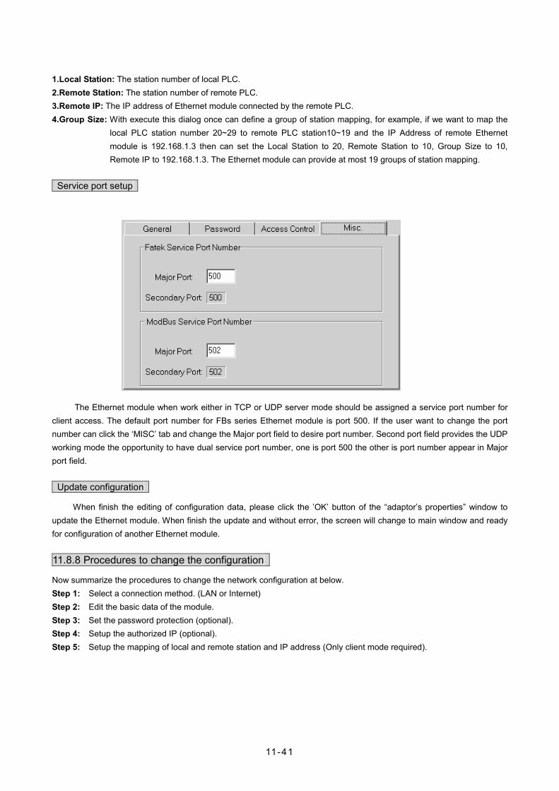
11-41
1.Local Station: The station number of local PLC. 2.Remote Station: The station number of remote PLC. 3.Remote IP: The IP address of Ethernet module connected by the remote PLC. 4.Group Size: With execute this dialog once can define a group of station mapping, for example, if we want to map the
local PLC station number 20~29 to remote PLC station10~19 and the IP Address of remote Ethernet module is 192.168.1.3 then can set the Local Station to 20, Remote Station to 10, Group Size to 10, Remote IP to 192.168.1.3. The Ethernet module can provide at most 19 groups of station mapping.
Service port setup
The Ethernet module when work either in TCP or UDP server mode should be assigned a service port number for client access. The default port number for FBs series Ethernet module is port 500. If the user want to change the port number can click the ‘MISC’ tab and change the Major port field to desire port number. Second port field provides the UDP working mode the opportunity to have dual service port number, one is port 500 the other is port number appear in Major port field. Update configuration
When finish the editing of configuration data, please click the ’OK’ button of the “adaptor’s properties” window to update the Ethernet module. When finish the update and without error, the screen will change to main window and ready for configuration of another Ethernet module. 11.8.8 Procedures to change the configuration
Now summarize the procedures to change the network configuration at below. Step 1: Select a connection method. (LAN or Internet) Step 2: Edit the basic data of the module. Step 3: Set the password protection (optional). Step 4: Setup the authorized IP (optional). Step 5: Setup the mapping of local and remote station and IP address (Only client mode required).

11-42
11.8.9 Pin assignments and protocols
RS232 port pin assignments
Signal Pins Direction
RX 2 External→PLC
TX 3 External←PLC
GND 5
RS485 port pin assignments
FATEK TCP/UDP communication protocol
The communication protocol of FATEK TCP/UDP embeds the FATEK serial communication message in the TCP or UDP data packet. The port number used to convey the FATEK TCP/UDP message is configurable (default is 500.)
ModBus/TCP communication protocol
The document of communication protocol of Modbus/TCP can be referenced at the web site http://www.modbus.org . The port number used to convey the Modbus/TCP message is 502.

12-1
Chapter 12 The Applications of FBs-PLC Communication Link
As previously revealed in Chapter 11 that the FBs-PLC can support the "Ladder Program Control Interface" communication function for the applications of multi_drop FATEK CPU Link network or connecting with the intelligent peripherals through Port 1~Port 4.
The connection of FBs-PLC can through CLINK(FUN151), besides it support ModBus communication interface,too. Port1~Port 4 can be ModBus communication protocol master station by FUN150 to connect with the ModBus slave peripherals.
The RS-232 interface is for point to point connection, the RS-485 interface is for long distance connection or multi-drop communication network
The FUN151 (CLINK) instruction provides MD0 to MD3 four kinds of instruction mode, that the MD3 mode is monopolized by Port 2 for “FATEK High Speed CPU Link Network” , the others are for “Ordinary Communication Link”. The following list enlisted the description for the difference on various instruction modes for the CLINK instruction
Item Category Baud Rate Data Length
Transmitting code
Error detection Command
processing speed
High Speed LINK (MD3)
* Port 2 only
38.4K bps |
921.6K bps8-bit
Binary code
CRC-16 Interrupt driven
FUN151
(CLINK) Ordinary LINK (MD0~MD2)
* Port 1~ Por t 4
4.8K bps |
921.6K bps
7-bit or 8-bit
AdjustableASCII code Checksum Normal scan
FUN150
(M-BUS)
ModBus
Master
4.8K bps |
921.6K bps8-bit Binary code CRC-16 Normal scan

12-2
12.1 Application for FUN151 instruction
12.1.1 Procedures for usage
Sta r t
Hardware wiring to connect the various stations (PLC, ASCII peripherals, etc.)
Set up the station number of the linking stations and make a consistent communication parameters setting for these stations.
Station number can be set to any one between 1 to 254 without replication.
Fill in the value to the communication interface register (Rxxxx) of FUN151 (CLINK) if necessary; properly adjust the Time_out timer to detect communication error, transaction delay to meet slow response device , etc.
For communication parameters, please refer to the description of "Communication Related Setting".
Write FUN151 instruction to PLC, which serves as the master station or performs communication sender/ receiver, and then fill the communication program into the register table assigned by operand SR. FUN151 will then automatically send or receive data according to the definition of communication program. The user can easily reach the various function services of CLINK by accessing the table like of communication program.
End
12.1.2 Explanation of respective modes and application program for FUN151
This section will base on the four instruction modes (MD0 to MD3) of FUN151 (CLINK) instruction to explain their usages, with respective practical application program examples.

FBs-PLC LINK
12-3
FUN151P CLINK
Convenient Instruction of FUN151: MD0 (Which makes PLC act as the master station in CPU LINK network through Port 1~4)
FUN151PCLINK
Pt :ENExecution
control
Ladder symbol
151P.CLINKACT
ERRPause PAU
Abort ABT
SR :
DN
WR :
MD :Acting
Error
Done
Pt : Assign the port, 1~4 MD : 0, serves as the master station of Fatek CPU
Link (employs Fatek communication protocol) SR : Starting register of communication program
(see example for its explanation) WR : Starting register for instruction operation (see
example for its explanation). It controls 8 registers, the other programs can not repeat in using.
HR ROR DR K Range Operand
R0 ∣
R3839
R5000∣
R8071
D0 ∣
D3999
Pt 1~4 MD 0 SR
WR *
Descriptions
1. FUN151: MD 0, it makes PLC act as the master of FATEK CPU Link Network through Port 1~ 4.
2. The master PLC may connect with 254 slave stations through the RS-485 interface.
3. Only the master PLC needs to use FUN151 instruction, the slave doesn't need.
4. It employs the program coding method or table filling method to plan for the data flow controls; i.e. from which one of the slave station to get which type of data and save them to the master PLC, or from the master PLC to write which type of data to the assigned slave station. It needs only seven registries to make definition; every seven registers define one packet of data transaction.
5. When execution control 〝EN〞changes from 0→1 and both inputs “PAU” and “ABT” are 0, and if Port 1/2/3/4 hasn’t been controlled by other communication instructions [i.e. M1960 (Port1) / M1962 (Port2) / M1936 (Port3) / M1938 (Port4) = 1], this instruction will control the Port 1/2/3/4 immediately and set the M1960/M1962/M1936/M1938 to be 0 (which means it is being occupied), then going on a packet of data transaction immediately. If Port 1/2/3/4 has been controlled (M1960/M1962/M1936/M1938 = 0), then this instruction will enter into the standby status until the controlling communication instruction completes its transaction or pause/abort its operation to release the control right (M1960/M1962/M1936/M1938 =1), and then this instruction will become enactive, set M1960/M1962/M1936/M1938 to be 0, and going on the data transaction immediately.
6. While in transaction processing, if operation control “PAU” becomes 1, this instruction will release the control right (M1960/M1962/M1936/M1938 = 1) after this transaction. Next time, when this instruction takes over the transmission right again, it will restart from the next packet of data transaction.
7. While in transaction processing, if operation control “ABT” becomes 1, this instruction will abort this transaction immediately and release the control right (M1960/M1962/M1936/M1938 = 1). Next time, when this instruction takes over the transmission right again, it will restart from the first packet of data transaction.
8. While it is in the data transaction, the output indication “ACT” will be ON.
9. If there is error occurred when it finishes a packet of data transaction, the output indication “DN” & “ERR” will be ON.
10. If there is no error occurred when it finishes a packet of data transaction, the output indication “DN” will be ON.

FBs-PLC LINK
12-4
FUN151P CLINK
Convenient Instruction of FUN151: MD0 (Which makes PLC act as the master station in CPU LINK network through Port 1~4)
FUN151P CLINK
【Interface Signals】
Dedicated Relays and Registers for corresponding port :
Comm. PortSignals
Port 1 Port 2 Port 3 Port 4
1. Port Ready Indicator M1960 M1962 M1936 M1938 2. Port Finished Indicator M1961 M1963 M1937 M1939
3. Port Communication Parameters R4146 R4158 R4043 R4044
4. TX Delay & RX Time-out Span R4147 R4159 R4045 R4048
1. Port Ready Indicator:This signal is generated from CPU. ON, it represents that port is free and ready.
OFF, it represents that port is busy, data transaction is going.
2. Port Finished Indicator : This signal is generated from CPU. When the communication program completed the last packet of data transaction, this signal will be ON for
one scan time (for successive data transaction). When the communication program completed the last packet of data transaction, this signal will be still
ON (for single packet of data transmission)
3. Port Communication Parameters : The register is for communication parameters setting of corresponding port. (please refer to the chapter of
communication parameters setting)
4. TX Delay & RX Time-out Span : The content of Low Byte defines the receive Time-out span of CLINK instruction; its unit is 0.01 second
(the default is 50, which means 0.5 second). The CLINK instruction employs receive Time-out span to judge whether the slave station on line or not. When the master PLC sent out the read/write command to the slave station, the slave station didn’t reply within this period means that there is abnormal event in communication called Time-out. When there are multi-drop linking, properly adjust this value (greater than 1 scan time of the slave station with the longest scan time) to shorten the communication response time among the active linking stations if there are many slave stations power off (The time-out cases will happen).
The content of High Byte defines the transmission delay time between two packets of data transaction for CLINK instruction; its unit is 0.01 second (the default is 0).

FBs-PLC LINK
12-5
FUN151P CLINK
Convenient Instruction of FUN151: MD0 (Which makes PLC act as the master station in CPU LINK network through Port 1~4)
FUN151P CLINK
Program example(Automatic cycling transmission)
1 5 1 P .C L IN K
P A U0M D :
R 5 1 0 0S R :
1P t : A C TM 1 0 0M 1
M 1 0 1E R R
M 1 0 2D NA B T
M 1 9 6 0
R 1 1 0W R :
1 5 1 P .C L IN K
R 1 2 0R 5 2 0 0
M 1 9 6 2M 22P t :
P A U
A B T
S R :W R :
M D :A C T
0E R R
D NM 1 0 5
M 1 0 4
M 1 0 3
1 5 1 P .C L IN K
R 1 3 0R 5 3 0 0
M 1 9 3 6M 33P t :
P A U
A B T
S R :W R :
M D :A C T
0E R R
D NM 1 0 8
M 1 0 7
M 1 0 6
1 5 1 P .C L IN K
R 1 4 0R 5 4 0 0
M 1 9 3 8M 44P t :
P A U
A B T
S R :W R :
M D :A C T
0E R R
D NM 1 1 1
M 1 1 0
M 1 0 9E N
E N
E N
E N
Explanation on program example
When there is communication error, gets and stores the error message, it would be helpful for error analysis or logging.
( + 1 )
S :D :
0 8 D . M O V
1 5 D
E N
E N
R 1 1 2 6R 1 4 0
R 1 1 0 6 O V F
( + 1 )
D :S :
( + 1 )
D :S :
0 8 D . M O V
1 5 D
0 8 D . M O V
1 5 D
E N
E N
E N
E N
R 1 1 2 4R 1 3 0
R 1 1 0 4 O V F
R 1 1 2 2R 1 2 0
R 1 1 0 2 O V F
( + 1 )
D :S :
1 5 D
0 8 D . M O V
E N
E N
R 1 1 0R 1 1 2 0
R 1 1 0 0 O V F
M 1 1 0
M 1 0 7
M 1 0 4
M 1 0 1

FBs-PLC LINK
12-6
FUN151P CLINK
Convenient Instruction of FUN151: MD0 (Which makes PLC act as the master station in CPU LINK network through Port 1~4)
FUN151P CLINK
Editing Communication Table with WinProladder
Click the “Link Table” Item which in project windows :
Project name
Table Edit
Link Table Click right button and select “New Link Table”
Table Type : MD0 must be selected ”Normal Link Table”. ; MD3 must be selected ”High Speed Link Table”.
Table Name : For modify or debug, you can give a convenient name.
Table Starting address : Enter the address which is the starting register of communication table to store the data exchange list.
※ To make it easy to edit, read, and maintain the communication program, we have extended following
related instructions under FUN150 and FUN151. The use method is take focus on FUN150 or FUN151, and press the hotkey “Z”. When “Table Edit” windows appear, then you can edit the communication table.

FBs-PLC LINK
12-7
FUN151P CLINK
Convenient Instruction of FUN151: MD0 (Which makes PLC act as the master station in CPU LINK network through Port 1~4)
FUN151P CLINK
Explanation for operand SR
SR:Starting register for communication program of CLINK instruction
SR+0 Total transactions • Low Byte is valid; one transaction takes 7 registers to describe,
which means 7 registers define a packet of data transaction.
SR+1 Slave station No. which is about
to transact with • Low Byte is valid, 0~254 (0 means that master PLC broadcasts
the data to all slave PLC, the slave PLC does not reply).
SR+2 Command code • Low Byte is valid; =1, means reading data from slave PLC;
=2, means writing data to slave PLC.
SR+3 Data length of this transaction • Low Byte is valid; the range is 1~64.
SR+4 Data type of Master PLC • Low Byte is valid, and its range is 0 to 13; it defines the data
type of master PLC (see next page).
SR+5 Starting reference of Master PLC • Word is valid; it defines the starting address of data (master).
SR+6 Data type of slave PLC • Low Byte is valid, and its range is 0 to 13; it defines the data
type of slave PLC (see next page).
SR+7 Starting reference of Slave PLC • Word is valid; it defines the starting address of data (slave).
SR+8 Slave station No. which is about to transact with
SR+9 Command Code
SR+10 Data length of this transaction
SR+11 Data type of Master PLC
SR+12 Starting reference of Master PLC
SR+13 Data type of slave PLC
SR+14 Starting reference of Slave PLC
Description of the 2nd packet of transaction.

FBs-PLC LINK
12-8
FUN151P CLINK
Convenient Instruction of FUN151: MD0 (Which makes PLC act as the master station in CPU LINK network through Port 1~4)
FUN151P CLINK
Master/Slave data type, code and reference number
Data code Data type Reference number 0 X (discrete input) 0~255 1 Y (discrete output) 0~255 2 M (internal relay M) 0~1911 3 S (step relay S) 0~999 4 T (timer contact) 0~255 5 C (counter contact) 0~255 6 WX (word of discrete input ,16 bits) 0~240, it must be the multiple of 8. 7 WY (word of discrete output ,16 bits) 0~240, it must be the multiple of 8. 8 WM (word of internal relay,16 bits) 0~1896, it must be the multiple of 8. 9 W S (word of step relay,16 bits) 0~984, it must be the multiple of 8.
10 TR (timer register) 0~255 11 CR (counter register) 0~199 12 R (data register Rxxxx) 0~3839 13 D (data register Dxxxx) 0~4095
Note : The data type for master and slave must be consistent. i.e. if the master station is any value between 0 to 5, the slave station must also be any value between 0 to 5; if the master station is any value between 6 to 13, the slave station must also be any value between 6 to 13.
Explanation for the operand WR of FUN151:MD0
High Byte Low Byte
WR+0 Result code Transaction No.
• Result code indicates the transaction result; 0= normal, other value=abnormal.
• Transaction No. indicates which one is in processing.
WR+1 Station number Command code
WR+2 For internal operation
WR+3 For internal operation
• Station number, the slave station No. which is in transaction. Command code =44H, reading successive discrete status from slave PLC. =45H, writing successive discrete status to slave PLC. =46H, reading successive registers from slave PLC. =47H, writing successive registers to slave PLC.
WR+4 For internal operation
WR+5 For internal operation
WR+6 For internal operation
WR+7 For internal operation
• WR+4’s b0=1, Port has been occupied and this instruction is waiting to acquire the transmission right for data transaction.
b4=1 , This instruction is not first time performing. b12 , Output indication for “ACT” b13 , Output indication for “ERR”. b14 , Output indication for “DN”.
Result code: 0, this transaction is successful. 2, data length error (data length is 0 or greater than 64 in one transaction). 3, command code error (command code is greater than 2). 4, data type error (data type is greater than 13, please refer to data type code). 5, reference number error (please refer to reference number). 6, inconsistence in data type (e.g. master station is 0~5 while slave is 6~13). A, no response from slave station (Time-out error). B, communication error (received error data).

FBs-PLC LINK
12-9
FUN151P CLINK
Convenient Instruction of FUN151: MD0 (Which makes PLC act as the master station in CPU LINK network through Port 1~4)
FUN151P CLINK
For easy programming and trouble shooting, the Winproladder provides the table editing environment to edit the communication table of FUN151 instruction; Key in the complete FUN151 instruction first and then move the cursor to the position of it, depressing the "Z" key, now comes the table editing environment. The user can create the new communication table or display the existed table under this friendly user interface operation.
Communication Table for FUN151:MD0
Sequence No.
Command Slave Master Data Slave Data Length
0 ~ nnn Read (=1) Write (=2)
Describing the station number of slave PLC which is about to transact with.
Station number=0,The master PLC broadcasts the data to all slave PLCs and slave PLCs will not reply Station number=N, it means the station number of the slave PLC which is about to transact with the master PLC N=1~ 254
Describing the data type & reference number of this packet of transaction for the master PLC. X0 ~ X255 Y0 ~ Y255 M0 ~ M1911 S0 ~ S999 T0 ~ T255 C0 ~ C255 WX0 ~ WX240 WY0 ~ WY240 WM0 ~ WM1896 WS0 ~ WS984 TR0 ~ TR255 CR0 ~ CR199 R0 ~ R3839 D0 ~ D4095
Describing the data type & reference number of this packet of transaction for the slave PLC. X0 ~ X255 Y0 ~ Y255 M0 ~ M1911 S0 ~ S999 T0 ~ T255 C0 ~ C255 WX0 ~ WX240 WY0 ~ WY240 WM0 ~ WM1896 WS0 ~ WS984 TR0 ~ TR255 CR0 ~ CR199 R0 ~ R3839 D0 ~ D4095
Data length of this transaction.
1 ~ 64
Explanation on program example
When execution control M1/M2/M3/M4 = 1, and corresponding port is not occupied by other communication instruction (M1960、M1962、M1936、M1938 = 1), CLINK instruction will start the data transaction. The M1960、
M1962、M1936、M1938 is OFF during data transaction, and when the transaction is finished, the M1960、
M1962、M1936、M1938 becomes ON. Employ the OFF↔ON change of M1960、M1962、M1936、M1938 (FUN151 execution control “EN↑” = 0→1 means starting) may automatically starts for every packet of data transaction successively (when the last packet of transaction is completed, it will automatically return to the first packet of transaction to obtain the automatic cycling transmission).
Output Indicators : 〝ACT〞ON:Transaction is in progress 〝ERR〞ON:Error occurred (Refer to the result code)
〝DN〞ON:One transaction finished

FBs-PLC LINK
12-10
FUN151P CLINK
Convenient Instruction of FUN151: MD0 (Which makes PLC act as the master station in CPU LINK network through Port 1~4)
FUN151P CLINK
Waveform of Input and Output signals
M1960M1962M1936M1938
ENU(start transmission)
ACT(data transmission)
DN(Non-error)
ERR(Error occur)
Note : 1. Only "DN" will be ON if one transaction finished without error.
2. "ERR" & "DN" will be ON at the same time if one transaction finished with error.
3. M1961/M1963/M1937/M1939 will be ON one scan time while the last packet of transaction finished.

FBs-PLC LINK
12-11
FUN151P CLINK
Convenient Instruction of FUN151: MD1 (Which makes PLC act as the communication sender through Port 1~4)
FUN151P CLINK
Pt :ENExecution
control
Ladder symbol
151P.CLINKACT
ERRPause PAU
Abort ABT
SR :
DN
WR :
MD :Acting
Error
Done
Pt : Assign the port, 1~4 MD : 1, link with intelligent peripherals that equipped
with communication interface SR : Starting register for data transmission table
WR : Starting register for instruction operation (see example for explanation). It controls 8
registers, the other programs cannot repeat in use.
HR ROR DR K Range
Operand
R0 ∣
R3839
R5000 ∣
R8071
D0 ∣
D3999
Pt 1~4 MD 1 SR
WR *
Descriptions
1. FUN151:MD1, it makes PLC act as the communication sender to link with the intelligent peripherals that equipped with communication interface.
2. A master PLC may connect to multi sets of peripherals that have identical communication protocol through the RS-485 interface.
3. The communication protocol/format is written with LADDER program, which must be consistent with the linked peripherals.
4. When execution control 〝EN〞changes from 0→1 and both inputs “PAU” and “ABT” are 0, and if Port 1/2/3/4 hasn’t been controlled by other communication instructions [i.e. M1960 (Port1) 、 M1962 (Port2) 、M1936
(Port3) 、 M1938 (Port4) = 1], this instruction will control the Port 1/2/3/4 immediately and set the M1960、
M1962、M1936、M1938 to be 0 (which means it is being occupied), then going on a packet of data transaction immediately. If Port 1/2/3/4 has been controlled (M1960、M1962、M1936、M1938 = 0), then this instruction will enter into the standby status until the controlling communication instruction completes its transaction or pause/abort its operation to release the control right (M1960、M1962、M1936、M1938 =1), and then this instruction will become enactive, set M1960、M1962、M1936、M1938 to be 0, and going on the data transaction immediately.
5. During transaction, if the “PAU” input becomes 1, this instruction will pause and release the control right (set M1960、M1962、M1936、M1938 = 1) after it completed the transmission of the on-going data.
6. During transaction, if the “ABT” input becomes 1, this instruction will abort the transmission and release the control right immediately (set M1960/M1962/M1936/M1938 = 1).
7. While transaction is going, the output indication “ACT” will be ON.
8. When a packet of data transaction is finished (transmission finished or "transmit then receive" completed), if there is error occurred, the output indication “DN” & “ERR” will be ON.
9. When a packet of data transaction is finished (transmission finished or "transmit then receive" completed), if there is no error occurred, the output indication “DN” will be ON.

FBs-PLC LINK
12-12
FUN151P CLINK
Convenient Instruction of FUN151: MD1 (Which makes PLC act as the communication sender through Port 1~4)
FUN151P CLINK
【Interface Signals】
Dedicated Relays and Registers for corresponding port :
Comm Port Signals
Port 1 Port 2 Port 3 Port 4
1. Port Ready Indicator M1960 M1962 M1936 M1938 2. Port Finished Indicator M1961 M1963 M1937 M1939
3. Port Communication Parameters R4146 R4158 R4043 R4044
4. TX Delay & RX Time-out Span R4147 R4159 R4045 R4048
5. New Message Detection Time Interval
R4148
1. Port Ready Indicator: This signal is generated from CPU. ON, it represents that port is free and ready. OFF, it represents that port is busy, data transaction is going.
2. Port Finished Indicator: This signal is generated from CPU. ON, it means data transaction has been completed.
3. Port Communication Parameters : The register is for communication parameters setting of corresponding. port. (please refer to the chapter
of communication parameters setting).
4. TX Delay & RX Time-out Span: The content of Low Byte defines the receive Time-out span of CLINK instruction; its unit is 0.01 second
(the default is 50, which means 0.5 second).
The CLINK instruction employs receive Time-out span to judge whether the slave station on line or not. When the master PLC sent out the read/write command to the slave station, the slave station didn’t reply within this period means that there is abnormal event in communication called Time-out. When there are multi-drop linking, properly adjust this value (greater than 1 scan time of the slave station with the longest scan time) to shorten the communication response time among the active linking stations if there are many slave stations power off (The time-out cases will happen).
The content of High Byte makes no sense at this mode.
5. New Message Detection Time Interval : While the communication port being used as the master or slave of ModBus RTU protocol, the system
will give the default time interval to identify each packet of receiving message, if the default works not well, the user can set this time interval through the high byte setting of R4148 and let M1956 be 1, to avoid the overlap of different packet of message frame.
M1956=0, the system default is 3×16 bits time period for Port1~Port4.
M1956=1, High Byte of R4148 is used to set the new message detection time interval for Port1~Port4( the range is 12~63, the unit is in 16-bit)
The actual time depends on the communication baud rate.

FBs-PLC LINK
12-13
FUN151P CLINK
Convenient Instruction of FUN151: MD1 (Which makes PLC act as the communication sender through Port 1~4)
FUN151P CLINK
While the communication port being used to communicate with the intelligent peripherals through the FUN151 convenient instruction, if the communication protocol without the end of text to separate each packet of message frame, it needs message detection time interval to identify the different packet. High byte of R4148 is used for this setting.
M1956=0, the system default is 3×16 bits time period for Port1~Port4.
M1956=1, High Byte of R4148 is used to set the new message detection time interval for Port1~Port4( the range is 12~63, the unit is in 16-bit)
The actual time depends on the communication baud rate.
Program example for loop back test
PLC station A sends data to PLC station B (PLC station B sends the received original data back to the PLC station A, loopback test), and checks whether the responding message of PLC station B is the same as its original data that had sent out; therefore, it can do simple test on software and hardware of PLC Port1 whether it is normal and error free.

FBs-PLC LINK
12-14
FUN151P CLINK
Convenient Instruction of FUN151: MD1 (Which makes PLC act as the communication sender through Port 1~4)
FUN151P CLINK
↑
( )
( )
( )
( )
S
08.MOV
: R 2: 4
: R 0
: 0203H: R 1
EN
M0
EN
DEN
ENDS
D
M1924
EN
EN
08.MOV
RST R 108
: 1S
08.MOV
08.MOV
: R 3: 2
DS
08.MOV: 4FH: R 4D
S
08.MOV: 4BH: R 5
EN
EN
DS
08.MOV
: R 6: 3
DS
M0
ERR
ACT
Y2
Y1
Y0
: R 108
: 0
Sa
Sba=b
a>b
a<b
M100
M100EN
66JMP 1
EN
ABT
PAU
DN
EN17.CMP
U/S
151P.CLINKPtMDSR : R0
: 1: 1
WR: R100
• Clears the received data length to be 0 (for "transmit" only, this instruction is not required).
• Setting of the operation mode: • Set to be "transmit then receive" mode (R0=1)
• Set the starting code (02H) and ending code (03H) for responding message in receiving. (without starting and ending codes, R1=0 can also receive regularly)
• Packing data to be transmitted: • Set the transmitting data length (R2=N).
• Fills in the data that is to be transmitted:
• Fill in data 1 (R3= ' STX ' )
• Fill in data 2 (R4= ' O ' )
• Fill in data 3 (R5= ' K ' )
• Fill in data 4 (R6= ' ETX ' )
• When selecting "transmit then receive" mode, it employs the comparing instruction to judge whether the responding message from the counter partner is received; if it is received, then M100=OFF, and it will process the received data. (For " transmit" mode, this program is not required)

FBs-PLC LINK
12-15
FUN151P CLINK
Convenient Instruction of FUN151: MD1 (Which makes PLC act as the communication sender through Port 1~4)
FUN151P CLINK
• The processing program for data received.
• For details of the data received, please refer to the explanation of following page.
( )
( )EN
17.CMP
a<b
a>b
a=bM101
: R 108: R 2Sb
Sa
D
M101
M101
EN
EN
S
JMP66
EN SET
0
Y 3
: 0: V
08.MOV
EN SaSb
R 2FOR70
17.CMP
a<b
M101
a>b
a=b: R 109V: R 3V
(+1)
NEXT
EN
71
EN SET
15
R 108
V
Y 4
65
LBL65
1
EN
LBL
RST
0
M101
U/S
U/S
• Compares the received data length and transmitted data length.
• When the length is inconsistent, it sets up the error indication.
• Clears the pointer V to be 0.
• Compares the consistency of all of the received data and transmitted data.
• Compares the received data and transmitted data one by one.
• When there is a data difference, set up the error indication.
• As the received data processed complete, clears the received data length to be 0, and gets ready to receive new data.

FBs-PLC LINK
12-16
FUN151P CLINK
Convenient Instruction of FUN151: MD1 (Which makes PLC act as the communication sender through Port 1~4)
FUN151P CLINK
Explanation for the operand SR of FUN151: MD1
SR:Starting register of data transmission table
SR+0 Transmit only or
Transmit then Receive
• Low byte is valid, 0: transmit only, no response from the slave 1: transmit then receive the responding message.
SR+1 Starting & Ending code
for receiving • High byte : Start of text for receiving. Low byte : End of text for receiving.
SR+2 Length of Transmission • The maximum length of data to be transmitted is 511
SR+3 Data 1 • Low byte is valid
SR+4 Data 2 • Low byte is valid
SR+5 Data 3 • Low byte is valid
Data 4
SR+6 ˙
˙
˙
Data N
• Low byte is valid • Low byte is valid
Note 1 : When selecting the transmit-only mode, the Starting /Ending code of receiving is meaningless.
2 : When it is in the "transmit then receive" mode, before the starting of transmission, it must first to estimate the starting and ending code of responding message from communication partner and write them into the receiving starting/ending code register (e.g. SR+1=0203H, 02H stands for starting code and 03H for ending code), so as to ensure the correct message frame receiving. The communication protocol with starting/ending code makes the identifying of every packet of messages easy, and the communication program is simple and efficient.
3 : When it is in the "transmit then receive" mode, fills the high byte of starting/ending code register with 0 if no starting code in responding message; if no ending code in responding message, fills 0 to the low byte of starting/ending code register. Adjusts the high byte of R4148 (message detection time interval) to judge whether a packet of data has been received completely; the unit is 0.001 second (the default is 0CH, 12mS). The communication protocol without ending code depends on message detection time interval to tell whether it has received completely a packet of data (the setting of message detection time interval must be greater than the maximum response delay time between data bytes when communication partner is replying), thus it may ensure the receiving of the whole packet to be complete. Generally speaking, the data in transmitting is transmitted one byte after another continuously; therefore, if there is pause (greater than message detection time interval), it means the packet of message is transmitted completely.

FBs-PLC LINK
12-17
FUN151P CLINK
Convenient Instruction of FUN151: MD1 (Which makes PLC act as the communication sender through Port 1~4)
FUN151P CLINK
Explanation for the operand WR of FUN151:MD1
High Byte Low Byte WR+0 Result code 0 • Result code =0, OK ; = other values, abnormal.
WR+1 For internal operation use
WR+2 For internal operation use
WR+3 For internal operation use
• Working registers for CLINK instruction
WR+4 For internal operation use
WR+5 For internal operation use
WR+6 For internal operation use
WR+7 For internal operation use
• WR+4 : b0=1, Pending b12=〝ACT〞output indication b13=〝ERR〞output indication b14=〝DN〞 output indication
WR+8 Total amount of data received • The total amount of data byte being received (the register for received
data length; it includes the starting and ending code).
WR+9 Data 1 • The first byte of data received (if there is the starting code, it is the
starting code); High byte =0.
Data 2 • The second byte of data received; High byte =0.
Data 3 • The third byte of data received; High byte =0.
˙
˙
˙
˙
Data N • The N_th byte of data received (if there is the ending code, it is the
ending code); High byte =0.
Result code : 0, transaction is successful.
2, data length error (the value is 0, or the packet of transaction is greater than 511)
A, no response from the slave
B, communication abnormal (received error data)
Output Indicator : 〝ACT〞 ON:Transaction is in progress
〝ERR〞 ON:Error occurred
〝DN〞 ON:One transaction finished

FBs-PLC LINK
12-18
FUN151P CLINK
Convenient Instruction of FUN151: MD2 (Which makes PLC act as the communication receiver through Port 1~4)
FUN151P CLINK
Pt :ENExecution
control
Ladder symbol
151P.CLINKACT
ERRPause PAU
Abort ABT
SR :
DN
WR :
MD :Acting
Error
Done
Pt : Assign the port, 1~4
MD : 2, PLC waiting to receive the message sent by intelligent peripherals
SR : Starting register for data transmission table
WR : Starting register for instruction operation (see example for explanation). It controls 8 registers, the other programs cannot repeat in use.
HR ROR DR K Range Operand
R0 ∣
R3839
R5000∣
R8071
D0 ∣
D3999
Pt 1~4 MD 2 SR
WR *
Descriptions
1. FUN151 : MD2 instruction provides Fatek PLC with ability to receive message sent by peripherals with communication interface at any time.
2. The communication protocol is written with LADDER program, which must be consistent to the peripheral device.
3. When execution control 〝EN〞changes from 0→1 and both inputs “PAU” and “ABT” are 0, and if Port 1/2/3/4 hasn’t been controlled by other communication instructions [i.e. M1960 (Port1) 、 M1962 (Port2) 、 M1936 (Port3) 、 M1938 (Port4) = 1], this instruction will control the Port 1/2/3/4 immediately and set the M1960、
M1962、M1936、M1938 to be 0 (which means it is being occupied). If Port 1/2/3/4 has been controlled (M1960、M1962、M1936、M1938 = 0), then this instruction will enter into the standby status until the controlling communication instruction completes its transaction or pause/abort its operation to release the control right, and then this instruction will become enactive.
4. When the input “PAU” or “ABT” becomes 1, it gives up the receiving immediately (M1960、M1962、M1936、
M1938 = 1).
5. While it is in the receiving state, the output indication “ACT” is ON.
6. When a packet of data transaction finished (receive finished or receive then transmit completed), if there is error occurred, the output indication “DN” & “ERR” will be ON for one scan time.
7. When a packet of data transaction finished (receive finished or receive then transmit completed), if there is no error occurred, the output indication “DN” will be ON for one scan time.

FBs-PLC LINK
12-19
FUN151P CLINK
Convenient Instruction of FUN151: MD2 (Which makes PLC act as the communication receiver through Port 1~4)
FUN151P CLINK
【 Interface Signals】
Dedicated Relays and Registers for corresponding port :
Comm Port Signals
Port 1 Port 2 Port 3 Port 4
1. Port Ready Indicator M1960 M1962 M1936 M1938 2. Port Finished Indicator M1961 M1963 M1937 M1939
3. Port Communication Parameters R4146 R4158 R4043 R4044
4. TX Delay & RX Time-out Span R4147 R4159 R4045 R4048
5. New Message Detection Time Interval
R4148
1. Port Ready Indicator: This signal is generated from CPU. ON, it represents that port is free and ready. OFF, it represents that port is busy, data transaction is going.
2. Port Finished Indicator: This signal is generated from CPU. ON, it means data transaction has been completed.
3. Port Communication Parameters : The register is for communication parameters setting of corresponding. port. (please refer to the chapter
of communication parameters setting).
4. TX Delay & RX Time-out Span: The Low Byte defines the Time-out span of FUN151:MD2 instruction; its unit is 0.01 second (the default
is 32H). When the PLC received the message and must respond to it (receive then transmit mode), but the LADDER program is unable to process and send out the responding message during this period of time, the CPU will give up response this time and automatically restore back to receiving state. When FUN151:MD2 is set to be "receive only" mode, this value is meaningless.
The content of High Byte makes no sense at this mode.
5. New Message Detection Time Interval: While the communication port being used as the master or slave of ModBus RTU protocol, the system
will give the default time interval to identify each packet of receiving message, if the default works not well, the user can set this time interval through the high byte setting of R4148 and let M1956 be 1, to avoid the overlap of different packet of message frame.
M1956=0, the system default is 3×16 bits time period for Port1~Port4.
M1956=1, High Byte of R4148 is used to set the new message detection time interval for Port1~Port4( the range is 12~63, the unit is in 16-bit)
The actual time depends on the communication baud rate.

FBs-PLC LINK
12-20
FUN151P CLINK
Convenient Instruction of FUN151: MD2 (Which makes PLC act as the communication receiver through Port 1~4)
FUN151P CLINK
While the communication port being used to communicate with the intelligent peripherals through the FUN151 convenient instruction, if the communication protocol without the end of text to separate each packet of message frame, it needs message detection time interval to identify the different packet. High byte of R4148 is used for this setting.
M1956=0, the system default is 3×16 bits time period for Port1~Port4.
M1956=1, High Byte of R4148 is used to set the new message detection time interval for Port1~Port4( the range is 12~63, the unit is in 16-bit)
The actual time depends on the communication baud rate. Note 1 : Once FUN151 : MD2 activated, it will stay in receiving state all the time; unless the input signal of PAU” or
“ABT” becomes ON, then it will escape from receiving state and stop receiving and waiting for next time it will be activated again.
2 : When there is change on Starting/Ending code for receiving, it must make the input signal of PAU” or “ABT” becomes ON once, and re-activate the receive control “EN” from 0→1 to start message receiving

FBs-PLC LINK
12-21
FUN151P CLINK
Convenient Instruction of FUN151: MD2 (Which makes PLC act as the communication receiver through Port 1~4)
FUN151P CLINK
Program example for loop back reply (This PLC station sends back the received data to the master, which had sent out the data)
( )
( )
( )
( )
D
EN SD
SEN
RSTEN
M1924RSTEN
R 2
R 108
08.MOV
08.MOV
: R 1: 0203H
: 1: R 0
EN SaSb
M2
M0
Y2RSTEN
a<b
a>b
a=bM100
DN
R 2
ERR
ACT
Y1
Y2
Y0
: R 108: 0
17.CMP
JMPEN66
R 108
1
08.MOV
103.BT_M
: R 3: R 109
: R 108
: R 2: R 108
65LBL 1
RSTEN
DSEN
LTdTsEN
M100
U/S
↑
151P.CLINK
: R100 : R0
: 1
WR
MD
SR
Pt: 2
EN
ABT
PAU
Clears the received data length to be 0.
• Clears the transmitted data length to be 0. (for ''receive' only, this program is not required).
• Sets up the operation mode:
• Sets “receive then transmit” mode.
• Sets up the starting code (02H) and ending code (03H) (R1=0, it will receive regularly even without the starting and ending code)
• When transmission complete, clears the transmitted data length to be 0 (for "receive" only mode, this instruction is not needed)
• While selecting "receive then transmit" mode, it employs the comparing instruction to tell whether a new packet of message is received; if it is, the M100=OFF and it will process the received data.
• Copy all of the received data to responding registers.
• R108 is the length of received data.
• After the received data processed, fills the received data length to be the sending back data length to start the responding transmission.
• Clears the received data length to be 0 (ready to receive new data).

FBs-PLC LINK
12-22
FUN151P CLINK
Convenient Instruction of FUN151: MD2 (Which makes PLC act as the communication receiver through Port 1~4)
FUN151P CLINK
Explanation for the operand SR of FUN151: MD2
SR : Starting register of data reply table
SR+0
Receive only or Receive then Transmit
• Low Byte is valid,
=0, "receive only" mode ; =1, "receive then transmit" mode
SR+1
Starting/Ending code of receiving
• High Byte : Describing the starting code of receiving
Low Byte : Describing the ending code of receiving.
Length of reply data
• Maximum of length is 511. It will satrt to transmitte the reply data as long as the length is not 0
Reply data 1 • Low Byte is valid
Reply data 2 • Low Byte is valid
SR+4 • • •
Reply data N • Low Byte is valid
Note 1 : When selecting the "receive only" mode, CPU fills the received data into the receiving registers and set the length after it has received a packet of message, and starts to receive the next packet of message immediately.
2 : When selecting the "receive then transmit" mode, CPU fills the received data into the receiving registers and set the length after it has received a packet of message; then it starts to wait for the reply data length which is not zero to start transmitting reply data (therefore when select this mode, it must control the reply data length to be zero before the reply data completely filled into the reply registers; when the reply data fills into the reply registers finished, it may then set the length of reply data).
3 : It must fills the starting code and ending code into the starting/ending code register before the starting of receiving (e.g. SR+1=0A0DH, 0AH stands for starting code and 0DH for ending code), so as to ensure it to be free from receiving error. The communication protocol with starting/ending code makes the identifying of every packet of messages easy, and the communication program is simple and efficient.
4 : If the receiving message without starting code, fills the high byte of starting/ending code with 0; if the receiving message without ending code, fills the low byte of starting/ending code with 0. Adjusting High Byte of R4148 (new message detection time interval) to detect whether a packet of message has been received completely, the unit is 0.001 second (default is 0CH, 12 mS). The communication protocol without ending code depends on new message detection time interval to tell whether it has received completely for a packet of data (the setting of new message detection time interval must be greater than the maximum delay time between data bytes to be received), thus it may ensure the receiving of the whole packet to be completed. Generally speaking, the data in transmitting is transmitted one byte after another continuously; therefore, if there is pause (greater than new message detection time interval), it means that the packet of message is transmitted completely.
5 : When selecting "receive only" mode, if the receiving message has no ending code, the interval between every packet of data sent by the sender must be greater than the receiver’s new message detection time interval, otherwise the receiver won’t be able to distinguish between each packet of data correctly.

FBs-PLC LINK
12-23
FUN151P CLINK
Convenient Instruction of FUN151: MD2 (Which makes PLC act as the communication receiver through Port 1~4)
FUN151P CLINK
Explanation for the operand WR of FUN151:MD2
High Byte Low Byte
WR+0 Result code 0 Result code =0, OK ; = other values, abnormal.
WR+1 For internal operation use
WR+2 For internal operation use
WR+3 For internal operation use
• Working registers for CLINK instruction
WR+4 For internal operation use
WR+5 For internal operation use
WR+6 For internal operation use
WR+7 For internal operation use
• WR+4 : b0=1, Pending b12=〝ACT〞output indication b13=〝ERR〞output indication b14=〝DN〞 output indication
WR+8 Total amount of data received • The total amount of data byte being received (the register for received
data length; it includes the starting and ending code).
WR+9 Data 1 • The first byte of data received (if there is the starting code, it is the
starting code); High byte =0.
‧
‧ Data 2 • The second byte of data received; High byte =0.
‧
‧ Data N • The N_th byte of data received (if there is the ending code, it is the
ending code); High byte =0.
Note : When CPU received a packet of message, it filled the data to receiving registers and set up the received data length. Before the LADDER program starts to receive, you may clear the register of received data length to be 0; it means the receiving of a new packet of message when compared and found that the received data length is not zero. After the LADDER program gets the received data, it clears the received data length register to be 0. Just compare to see the received data length register is not zero means the receiving of a packet of new message, and so it may easily to process the receiving action.
Result code : 0, data transaction is successful. 2, the data length is error (the value is 0, or the transaction is greater than 511) A, unable to reply message within Time-out span ("receive then transmit" mode). B, communication abnormal (received error data)
Output indication : “ACT” ON : In receiving state “ERR” ON : Error occurred in previous packet of transaction, it will be ON for a scan time
“DN” ON : The previous packet of transaction completed without error, ON for a scan time.

FBs-PLC LINK
12-24
FUN151P CLINK
Convenient Instruction of FUN151: MD3 ( PLC serve as the master of “Fatek high speed CPU Link network” through Port2)
FUN151PCLINK
Pt :ENExecution
control
Ladder symbol
151P.CLINKACT
ERRPause PAU
Abort ABT
SR :
DN
WR :
MD :Acting
Error
Done
Pt : Only port 2 is valid MD : 3, serves as the master station of Fatek High
Speed CPU Link network SR : Starting register of communication program (see example for its explanation)
Pt : Starting register for instruction operation (see example for its explanation). It controls 8 registers, the other programs can not repeat in using.
HR ROR DR K Range Operand
R0 ∣
R3839
R5000∣
R8071
D0 ∣
D3999
Pt 1~2 MD 3 SR
WR *
Descriptions
1. FUN151 : MD3, it provides high speed data sharing between Fatek's PLC (data response time will not be influenced by the scan time of PLC).
2. A master PLC can link with 254 slave PLCs at the most to share data through the RS-485 interface.
3. FUN151 : MD3 is required only by master PLC, not by the slave PLC.
4. The station number of master PLC must be No.1, or it should be assigned by R4054 register if which is not No.1 but need to be as the master.
5. The setting of M1958 for slave PLC must be ON (M1958 OFF is for non-high speed link), but it’s not necessary for master PLC.
6. In high speed linking, the maximum Baud Rate is 921.6K bps and minimum is 38.4K bps (adjustable); the data length is fixed at 8 Bits. Data is transmitted with binary code (which is twice time as fast as ASCII Code), and the error checking is adopting CRC-16, which is more reliable than Checksum.
7. The principle of high speed linking data transmission is based upon the COMMON DATA MEMORY concept to design; e.g. as the master PLC sent out the content of R0 to R31, .the contents of R0~R31 for all the slave PLCs will be the same as the master’s; when slave PLC no.2 sent out the contents of R32~R47, the R32~
R47 contents of master PLC and other slave PLCs will be the same as PLC station no.2’s, etc.
8. When PLC is in STOP mode, the Port 2 enters into the standard interface mode that it can connect to WinProladder, MMI, or graphic supervisor (the communication parameter is set by R4158).
9. It employs the program coding or table filling method to plan for data flow control; i.e. for what kind of data being sent from which PLC station to all the PLC on line, it takes only 7 registers (5 of which is being physically used, and 2 reserved) to define; every 7 registers define once communication transaction.
10. When execution control “EN” changes from 0→1 and both pause “PAU” and abort “ABT” are 0, this instruction will control Port 2 and set M1962 to be “0” (being controlled) and processing the data transaction immediately, suppose the Port 2 is not controlled by other communication instruction (M1962=1). If Port 2 is being controlled (M1962=0), this instruction will enter into wait state until the controlling instruction completes the transmission or pause/abort the operation to release the control right (M1962=1); then it enacts from wait state, engages in the transmitting transaction and sets M1962 to be “0”.
FBs-PLC LINK
12-25
FUN151P CLINK
Convenient Instruction of FUN151: MD3 ( PLC serve as the master of “Fatek high speed CPU Link network” through Port2)
FUN151PCLINK
11. When pause “PAU” or abort “ABT” of input is 1, it escapes from high speed data link immediately (M1962 ON).
12. Within the high speed linking, the output indication “ACT” is ON; Port 2 is occupied.
13.When there is error occurred while it is starting the high speed linking, the output indication “ERR” will be ON, and the high speed linking will not be performed.
【Interface signals】
M1958 : While in the PLC high speed data linking, slave PLC must set M1958 ON (not necessary for master PLC) For non high speed data linking of PLC, the slave PLC must set M1958 OFF.
M1962 : The signal is generated from CPU. ON represents the Port 2 is available. OFF represents the Port 2 is occupied.
M1963 : The signal is generated from CPU. When M1967 is ON (this signal is controlled by the user program) and after the last packet of communication transaction is completed, the CPU sets M1962 and M1963 ON, and the high speed data transmission will be stopped; it must control “ABT” (transmission abort) to be ON, and then restart execution control “EN↑” to change from 0→1 before the high speed linking can restart. When M1967 is OFF (this signal is controlled by the user program), the high speed data transmission will automatically restart a new transmission from the first packet of communication transaction (M1962 and M1963 is keeping OFF state) after the last packet of communication transaction is completed.
M1967 : One-time or cycling control (controlled by the user program) ON, one cycle, it will stop after the last packet of data transaction is performed completely. OFF, successive cycles, it will restart from first packet of transaction when it has finished the last packet of transaction.
R4054 : It assigns the PLC station which is not no.1 to act as the master of high speed linking. High byte Low byte
R4054 55 Station number. H When the station number of the PLC is not number 1, fills its station number (low byte of R4055 stores the station number) into the low byte of R4054 and writes to high byte of R4054 with 55H, and then controls the execution control input “EN↑” from 0→1; even though the PLC station which is not no.1, it can still be the master station for high speed linking.
R4055 : When high byte of R4055 is not 55H,Low byte of R4055 shows the station number of PLC. When high byte of R4055 is 55H,Low byte of R4055 defines the station number of PLC.
R4058 : Showing the station number of slave PLC which is abnormal while high speed linking (0: Represents normal; if many slave PLC were abnormal in the mean time, it is possible to see only one number; after the debugging of abnormal and clear R4058 to be 0 until the value of R4058 keeping to be 0, it will then network works normal). In communication transaction program or table, it must exist the case for slave station to send data to other stations then can the master PLC detect whether the slave station is online without error; if in the communication transaction program or table, there is only the master station sending data to slave stations, the master PLC can’t detect whether slave PLC is on line without error. The user must employ programming skill to add abnormal detecting program to the master PLC and

FBs-PLC LINK
12-26
FUN151P CLINK
Convenient Instruction of FUN151: MD3 ( PLC serve as the master of “Fatek high speed CPU Link network” through Port2)
FUN151PCLINK
slave PLC to do the error checking (as a matter of fact, the program is very simple; just makes the PLC, which is sending data, to create an ON↔OFF variation signal. Once the receiving PLC does not detect the ON↔OFF variation signal in a period of time, it means that there is communication error).
R4059 : Error logging of abnormal slave PLC while high speed linking.
High byte Low byte R4059 Abnormal code Abnormal count H
Low byte : Abnormal count summation
High byte : Abnormal code OAH, No response from slave station OBH, Error data 01H, Framing Error 02H, Over_Run Error 04H, Parity Error 08H, CRC error
Explanation for the checking method for abnormal communication is the same as that for R4058.
R4160 : Port 2 Rx/Tx Time-out setting (in high speed linking). The system will base on the setting of R4161 communication parameter to produce pertaining set point if high byte of R4160 is not 56H, the user need not to set it. If high byte of R4160 is 56H, the low byte of R4160 is reserved for manual setting.
R4161 : Communication parameter setting register for Port 2 High Speed CPU Link.
Program example 1 (PLC no. 1 serves as the master of high speed data linking)
M100ABT
PAU
M0
M2
M1
3MD:
WR:SR:
R100R5000
151P.CLINK
Pt : 2
ERR
DN
ACT
M100M1963 M1967
EN
• Planning R5000~R5199 to be ROR, the communication program will be stored together with LADDER program.
• When M1967 is ON, performs one cycle transmission. It must start the abortion, then restart M0 before it can perform high speed data link again.

FBs-PLC LINK
12-27
FUN151P CLINK
Convenient Instruction of FUN151: MD3 ( PLC serve as the master of “Fatek high speed CPU Link network” through Port2)
FUN151PCLINK
Program example 2 (PLC which station number is not no.1 serves as the master of high speed data linking.)
M1ABT
PAU
M0EN
M3
M2
3MD:
WR:SR:
R100R5000
151P.CLINK
Pt : 2
ERR
DN
ACT
R4055
D :Sb :
R40545500H
EN
EN
19.OR
Sa : D=0
R4055
D :
Sa :Sb :
R4054
D=0
18.ANDM0
00FFH
Program example 3
The same machine sets or equipments (with same LADDER program) perform multi-station data collection or distributed control through RS-485 high speed linking.
The principle for high speed data linking is based on COMMON DATA MEMORY concept to design; while designing, it must devise a successive data block and evenly distributed to respective PLCs to do data exchange among PLCs. e.g.:
R1000~R1031: The data block of PLC no. 1 (through high speed linking, the other PLCs’ content of R1000~R1031 become the same as that of PLC no.1).
R1032~R1063: The data block of PLC no. 2 (through high speed linking, the other PLCs’ content of R1032~R1063 become the same as that of PLC no.2).
• • • • • •
For example, get the production data (stored at R0~R31) from each machine set, and collectively gathering R1000~R1639 (suppose there are 20 sets linking) stored in master PLC through RS-485 high speed data linking; it needs merely the master PLC of high speed linking to connect to MMI or graphic supervisor, then it can monitor and store, for follow up processing, the production data of respective machine sets with real time effect.
Note : If it is simply for data collection and monitoring and no need to do real time control, employs the FUN151: MD0 can easily and concisely accomplish the assignment; when requiring real time control or supervisoring , it must employ FUN151: MD3 to accomplish a speedy, precisely controlling demand.
• Get PLC station number and write it into R4054
• Set the high byte for R4054 to be 55H
• Planning R5000~R5199 to be ROR, the communication program will be stored together with LADDER program.
• When ABT is not controlled, M1 instruction needs not to input.

FBs-PLC LINK
12-28
FUN151P CLINK
Convenient Instruction of FUN151: MD3 ( PLC serve as the master of “Fatek high speed CPU Link network” through Port2)
FUN151PCLINK
D=0R4055Sa :EN
EN
EN
EN
Td : R 1000ZR 2000D :
13.(*)
R 2000
R 0
103.BT_M
Ts :
ZZ
Sb :D :
Sa :
D<0
D=0
(-1)16
Z
Sb :D : Z
UDF
18.AND
00FFH
• Get PLC station number and write it in pointer Z
• Station number deducts 1
• R2000 = Length of data to be sent from each station (e.g. 32) • data length * (station number−1):
Directing to the apportioned data block of this station.
• Move production data from respective stations to the apportioned data block of respective stations, and transmitting it to all other PLCs on line through high speed data linking.
Explanation for operand SR of FUN151: MD3
SR:Starting register for communication program of CLINK instruction
SR+0 Packets of data
transaction • Low Byte is valid. A packet of transmission demands 7 registers
to describe; i.e. 7 registers define a packet of data.
SR+1 Station number to transmitt • Low Byte is valid. 1~254
SR+2 Command code • Low Byte is valid, it can only be 4 (high speed linking command).
SR+3 Length of this packet of
data • Low Byte is valid. 1 ~ 32, defines the data length of one
transaction.
SR+4 Data type • Low Byte is valid. 12=R; 13=D.
SR+5 Data starting reference • Word is valid. Defines starting number of working data.
SR+6 Reserved
SR+7 Reserved
• Code for data type Data starting reference 12: R data register 0~3839 13: D data register 0~3999
SR+8 Station number to transmitt
SR+9 04
‧ Length of data
‧ Data type
‧ Data starting reference
‧ Reserved
‧ Reserved
Describing for the 2_nd packet of transaction

FBs-PLC LINK
12-29
FUN151P CLINK
Convenient Instruction of FUN151: MD3 ( PLC serve as the master of “Fatek high speed CPU Link network” through Port2)
FUN151PCLINK
Explanation for operand WR of FUN151:MD3
High Byte Low Byte WR+0 Result code WR+1 For internal operation
WR+7 For internal operation
Result code : 0 : Correct format 2 : Data length error (Length is 0 or greater than 32) 3 : Command code error (Command is not equal to 4) 4 : Data type error (Data type is not 12 nor 13) 5 : Data reference error
For easy programming and trouble shooting, the Winproladder provides the table editing environment to edit
the communication table of FUN151 instruction; Key in the complete FUN151 instruction first and then move the cursor to the position of it, depressing the "Z" key, now comes the table editing environment. The user can create the new communication table or display the existed table under this friendly user interface operation.
Communication Table for FUN151:MD3
※ Only Port 2 is valid for FUN151:MD 3
Sequence No.
Command Station No. Data All Station Length
0~nnn
High Speed Link ( =4 )
Station number to transmitt the data
1~254
The data will be transmtted R0~R3839 D0~D3999
The data will be received R0~R3839 D0~D3999
Data length of this transaction
1~32

FBs-PLC LINK
12-30
FUN151P CLINK
CPU Link by Way of Port 1 to Connect to Modem FUN151P
CLINK
PLC can connect to MODEM through communication port 1, and by way of telecommunication network to link and share data with remote PLC. Its application is as follows :
.Perform automatic data collection from the remote end. .Automatically report for alarm and abnormal conditions. .Associate with current available graphic supervisoring software or MMI etc. standard products to constitute a
wide area network automatic monitoring system. It doesn’t need to develop specific designing, so as to reduce the development risk and time limit.
Hardware configuration, and setting :
SCADAor
MMIor
WinProladder
MODEM
(Data reply PLC)
MODEM
(Data collection PLC)
FBS-PLC FBS-PLC
Data collecting PLC : .Don’t need to store phone number within the CPU .High Byte of R4149 = 55H (MODEM function) Data reply PLC : .High Byte of R4149 = 55H (MODEM function) .R4140~R4145 sets the phone number for general data
collecting PLC end (extension phone function allowed). e.g. Phone number is 02-28082192, then R4140=8220H, R4141=1280H, and R4142=0E29H.
MODEM
FBS-PLC
(Data reply PLC)
If phone number is : 02-28082192 ext 100, then R4140=2A20H, R4141=2808H, R4142=A291H, R4143=AAAAH, R4144=001AH, R4145=000EH. .Explanation: R4140~R4145 is telephone number register for dialing;
“E” is the ending character of phone number; “A” is the dial delaying character (usually the dialing of extension number or international long distance call can be reached by making use of dial delaying, the delayed time for a delaying character is based on MODEM setting, which is about 2 second). “B” stands for “#” character (can dial B. B. CALL), and “C” stands for “*” character.
.It employs CLINK (FUN151:MD0) instruction to write data to the general data collecting PLC or to read data from general data collecting PLC (refer to FUN151:MD0 Instruction user guide).
*** The maximum communication Baud Rate can reach 115200 bps (both of the communication ends must be consistent in setting)
.Let the communication parameters be 8-bit and Non-parity will be better for almost Modem

FBs-PLC LINK
12-31
FUN151P CLINK
CPU Link by Way of Port 1 to Connect to Modem FUN151P
CLINK
.The wiring of PLC communication port1 and MODEM: Fatek PLC (DB-9) MODEM (DB-25)
PIN 3:RXD ←→ TXD (PIN_3) PIN 2:TXD ←→ RXD (PIN_2) PIN 8:RTS ←→ CTS (PIN_4) PIN 7:CTS ←→ RTS (PIN_5) PIN 5:SG ←→ SG (PIN_7)
DSR (PIN_6) DTR (PIN_20)
MODEM dialing interface signal M1959 : OFF, dialing by “Tone” ; ON, dialing by “Pulse”
M1964 : OFF→ON, dial up ;
ON→OFF, hang up
R4163 : The Low Byte of R4163 is used to control the application of X instruction while MODEM dialing. =1, it does not detect dial tone nor busy tone while MODEM dialing. =2, it detects only dial tone but does not detect busy tone while MODEM dialing. =3, it dials directly without detecting dial tone, but will detect busy tone after MODEM dialing. =4, it detects both dial tone and busy tone for MODEM dialing. For other values, it works as 4; different country system needs to adjust the setting pertaining to the country.
The High Byte of R4163 is used to set the ring count for auto answer mode of Modem.
M1964(LADDER)
M1965(CPU)
M1966(CPU)
Hang upDial up Dial up Hang up
Connect
Disconnect Disconnect
Connect
Note 1 : Of M1965 and M1966, there will be only one ON, not both to be ON at the same time.
2 : The waiting time for dial connection is 1 minute; if unable to connect, it will redial twice (totally 3 times). If all of the dial connection tries failed, CPU will set M1966 to be ON (connection failed).
3 : When the quality of communication is not stable and easy to disconnect, you may employ the abnormal detecting function of CLINK instruction to control M1964 redials for connection (delay time of redial must be more than 10 seconds).
4 : When PLC change from RUN to STOP, the CPU will automatically change MODEM to be receiving state, which could accept the remote side dial connection.
5 : When PLC is not in dialing or MODEM connection states, CPU will automatically change MODEM to be receiving state, which could accept the remote side dial connection.

FBs-PLC LINK
12-32
FUN151P CLINK
CPU Link by Way of Port 1 to Connect to Modem FUN151P
CLINK
Program example
15 1 P .C L IN K
R 1 00R 50 0 0
M 1 96 5M 1 9 6 01P t :E N
P A U
A B T
S R :W R :
M D :A C T
0E R R
D NM 1 0 2
M 1 0 1
M 1 0 0
M 0
C U P
P V :C 0
S E T
E N
E N
3
M 1 9 64
E NC 0
M 1 9 64R S T
M 1 9 66
P L SP V :C 0
3
C U PM 1 9 61
C L R
C 0
P LS
When M0 changes from 0→1, dials up.
Clears the transaction count.
Hang up after transactions completed or connection failed.
Planning R5000~R5199 to be ROR, the communication program will be stored together with LADDER program.
Counting after all transactions completed

12-33
12.2 Application for FUN150( ModBus ) instruction
12.2.1 Procedures for usage
Star t
Hardware wiring to connect the various stations (PLC, ASCII peripherals, etc.)
Set up the station number of the linking stations and make a consistent communication parameters setting for these stations.。
Station number can be set to any one between 1 to 254 without replication.
Fill in the value to the communication interface register (Rxxxx) of FUN150 (ModBus) if necessary; properly adjust the Time_out timer to detect communication error, transaction delay to meet slow response device , etc.
For communication parameters, please refer to the description of "Communication Related Setting".
Write FUN150 instruction to PLC, which serves as the master station or performs communication sender/ receiver, and then fill the communication program into the register table assigned by operand SR. FUN150 will then automatically send or receive data according to the definition of communication program. The user can easily reach the various function services of ModBus by accessing the table like of communication program.
End
12.2.2 Explanation application program for FUN150
This section will instruction to explain FUN150(ModBus) usages, with respective practical application program examples.

FBs-PLC LINK
12-34
FUN150P M-BUS
Convenient Instruction for Modbus RTU Master (Which makes PLC as the Modbus RTU master through Port 1~4)
FUN150P M-BUS
Pt :1~4,specify the communication port to work as the Modbus RTU master
SR :Starting register of communication program WR :Starting register for instruction operation. It controls
8 registers,the other programs can not repeat in using.
HR ROR DR K Range
Ope- rand
R0 ∣
R3839
R5000∣
R8071
D0 ∣
D3999
Pt 1~4SR WR *
Descriptions
1. FUN150 (M-BUS) instruction makes PLC act as Modbus RTU master through Port 1~4, thus it is very easy to communicate with the intelligent peripheral with Modbus RTU protocol.
2. The master PLC may connect with 247 slave stations through the RS-485 interface. 3. Only the master PLC needs to use M-BUS instruction. 4. It employs the program coding method or table filling method to plan for the data flow controls; i.e. from which
one of the slave station to get which type of data and save them to the master PLC, or from the master PLC to write which type of data to the assigned slave station. It needs only seven registries to make definition; every seven registers define one packet of data transaction.
5. When execution control 〝EN〞changes from 0→1 and the input “ABT” is 0, and if Port 1/2/3/4 hasn’t been controlled by other communication instructions [i.e. M1960 (Port1)、 M1962 (Port2) 、 M1936 (Port3) 、 M1938 (Port4) = 1], this instruction will control the Port 1/2/3/4 immediately and set the M1960、M1962、
M1936、M1938 to be 0 (which means it is being occupied), then going on a packet of data transaction immediately. If Port 1/2/3/4 has been controlled (M1960、M1962、M1936、M1938 = 0), then this instruction will enter into the standby status until the controlling communication instruction completes its transaction or pause/abort its operation to release the control right (M1960、M1962、M1936、M1938 =1), and then this instruction will become enactive, set M1960、M1962、M1936、M1938 to be 0, and going on the data transaction immediately.
6. While in transaction processing, if operation control “ABT” becomes 1, this instruction will abort this transaction immediately and release the control right (M1960、M1962、M1936、M1938 = 1). Next time, when this instruction takes over the transmission right again, it will restart from the first packet of data transaction.
7. While〝A/R〞=0,Modbus RTU protocol;〝A/R〞=1,Modbus ASCII protocol (Reserved)。 8. While it is in the data transaction, the output indication “ACT” will be ON. 9. If there is error occurred when it finishes a packet of data transaction, the output indication “DN” & “ERR” will
be ON. 10. If there is no error occurred when it finishes a packet of data transaction, the output indication “DN” will be
ON.
Note : ModBus ASCII Mode will support after OS Version 4.12

FBs-PLC LINK
12-35
FUN150P M-BUS
Convenient Instruction for Modbus RTU Master (Which makes PLC as the Modbus RTU master through Port 1~4)
FUN150P M-BUS
【 Interface Signals】
Dedicated Relays and Registers for corresponding port :
Comm Port Signals
Port 1 Port 2 Port 3 Port 4
1. Port Ready Indicator M1960 M1962 M1936 M1938 2. Port Finished Indicator M1961 M1963 M1937 M1939
3. Port Communication Parameters R4146 R4158 R4043 R4044
4. TX Delay & RX Time-out Span R4147 R4159 R4045 R4048
5. New Message Detection Time Interval
R4148
1. Port Ready Indicator:This signal is generated from CPU. ON, it represents that port is free and ready.
OFF, it represents that port is busy, data transaction is going.
2. Port Finished Indicator : This signal is generated from CPU. When the communication program completed the last packet of data transaction, this signal will be ON for
one scan time (for successive data transaction). When the communication program completed the last packet of data transaction, this signal will be still
ON (for single packet of data transmission)
3. Port Communication Parameters : The register is for communication parameters setting of corresponding port. (please refer to the chapter of
communication parameters setting).
4. TX Delay & RX Time-out Span : The content of Low Byte defines the receive time-out span of M-BUS instruction; its unit is 0.01 second
(the default is 50, which means 0.5 second) The M-BUS instruction employs receive time-out span to judge whether the slave station on line or not. When the master PLC sent out the read/write command to the slave station, the slave station didn’t reply within this period means that there is abnormal event in communication called Time-out. When there are multi-drop linking, properly adjust this value (greater than 1 scan time of the slave station with the longest scan time) to shorten the communication response time among the active linking stations if there are many slave stations power off (The time-out cases will happen).
The content of High Byte defines the transmission delay time between two packets of data transaction for M-BUS instruction; its unit is 0.01 second (the default is 0).
For point to point link, this value can be set as 0 to shorten the communication transaction time and promote the communication efficiency. In the case of linking multi-drop and if the scan time of master PLC is far longer than any slave station, this value can also be set to 0 to shorten the communication transaction time and promote the communication efficiency. When there are multi-drops linking and the scan time of master PLC is close to that of slave station's, it must properly adjust this value (greater than 1 scan time of the slave station with the longest scan time) to reach the best, error-free communication quality

FBs-PLC LINK
12-36
FUN150P M-BUS
Convenient Instruction for Modbus RTU Master (Which makes PLC as the Modbus RTU master through Port 1~4)
FUN150P M-BUS
5. New Message Detection Time Interval : While the communication port being used as the master or slave of ModBus RTU protocol, the system will
give the default time interval to identify each packet of receiving message, if the default works not well, the user can set this time interval through the high byte setting of R4148 and let M1956 be 1, to avoid the overlap of different packet of message frame.
M1956=0, the system default is 3×16 bits time period for Port1~Port4.
M1956=1, High Byte of R4148 is used to set the new message detection time interval for Port1~Port4( the range is 12~63, the unit is in 16-bit)
The actual time depends on the communication baud rate. While the communication port being used to communicate with the intelligent peripherals through the
FUN150 convenient instruction, if the communication protocol without the end of text to separate each packet of message frame, it needs message detection time interval to identify the different packet. High byte of R4148 is used for this setting.
M1956=0, the system default is 3×16 bits time period for Port1~Port4.
M1956=1, High Byte of R4148 is used to set the new message detection time interval for Port1~Port4( the range is 12~63, the unit is in 16-bit)
The actual time depends on the communication baud rate.
Program example (Automatic cycling transmission)
A /R
E NR 5 0 0 0S R :
1P t : A C TM 1 0M 1
M 1 1E R R
M 1 2D NA B T
M 1 9 6 0
D 0W R :
D 2 0R 5 2 0 0
M 1 9 6 2M 22P t :E N
A B T
S R :W R :
A C T
E R R
D NM 2 2
M 2 1
M 2 0
S :
0 8 D .M O V
D :E N D 2 0
D 1 0 0 2
M 2 1
M 1 1E N S :
D : D 1 0 0 0
0 8 D .M O V
D 0
A /R
1 5 0 P .M _ B U S
1 5 0 P .M _ B U S
• Configure R5000~R5399 as the read only register (ROR) before programming, after then, when storing program, the ladder program will automatically contains the communication program .
• When there is communication error, gets and stores the error message to D1000 & D1001 would be helpful for error analysis or logging.

FBs-PLC LINK
12-37
FUN150P M-BUS
Convenient Instruction for Modbus RTU Master (Which makes PLC as the Modbus RTU master through Port 1~4)
FUN150P M-BUS
Explanation on program example 1. When execution control 〝EN〞changes from 0→1, and Port 1 is not occupied by other communication
instruction (M1960 ON), M-BUS instruction will start the data transaction. The M1960 is OFF during data transaction, and when the transaction is finished, the M1960 becomes ON. Employ the OFF←→ON change of M1960 (M-BUS execution control “EN” = 0→1 means starting) may automatically starts for every packet of data transaction successively (when the last packet of transaction is completed, it will automatically return to the first packet of transaction to obtain the automatic cycling transmission).
2. When execution control 〝EN〞changes from 0→1, and Port 2 is not occupied by other communication instruction (M1962 ON), M-BUS instruction will start the data transaction. The M1962 is OFF during data transaction, and when the transaction is finished, the M1962 becomes ON. Employ the OFF←→ON change of M1962 (M-BUS execution control “EN” = 0→1 means starting) may automatically starts for every packet of data transaction successively (when the last packet of transaction is completed, it will automatically return to the first packet of transaction to obtain the automatic cycling transmission).
Editing Communication Table with WinProladder
Click the “ModBus Master” Item which in project windows :
Project name
Table Edit
ModBus Master Click right button and select “Add ModBus Master Table”

FBs-PLC LINK
12-38
FUN150P M-BUS
Convenient Instruction for Modbus RTU Master (Which makes PLC as the Modbus RTU master through Port 1~4)
FUN150P M-BUS
Table Type : It will be fixed to ” ModBus Master Table ”.
Table Name : For modify or debug, you can give a convenient name.
Table Starting address : Enter the address which Starting register of communication Table

FBs-PLC LINK
12-39
FUN150P M-BUS
Convenient Instruction for Modbus RTU Master (Which makes PLC as the Modbus RTU master through Port 1~4)
FUN150P M-BUS
Starting register for communication program of M-BUS instruction
SR:Starting register for communication program of M-BUS instruction
A5h 50h SR+0
SR+1 07h Total
transactions
• A550h,it means valid M-BUS program
• Low Byte:Total number of transactions,one transaction needs 7 registers to describe.
SR+2 Slave station No. Which is
about to transact with • Low Byte is valid, 0~247 (0 means that master PLC broadcasts
the data to all slaves, the slaves do not reply).
SR+3 Command code • Low Byte is valid ; =1, means "Read data from slave station" =2, means"Write multiple data to slave station" =3, means "Write singal data to slave station"
SR+4 Data length of this
transaction • Low Byte is valid; the range is 1~125 (Reg.) or 1~255 (Dis).
SR+5 Data type of Master PLC • Low Byte is valid, and its range is 1~3 or 12~13; it defines the
data type of master PLC (see next page).
SR+6 Starting reference of
Master PLC • Word is valid; it defines the starting address of data (master).
SR+7 Data type of slave station • Low Byte is valid, and its range is 0 or 4; it defines the data type
of slave station (see next page).
SR+8 Starting reference of
Slave station • Word is valid; it defines the starting address of data (slave).
SR+9 Slave station No. which is
about to transact with
SR+10 Command code
SR+11 Data length of this
transaction
SR+12 Data type of Master PLC
SR+13 Starting reference of
Master PLC
SR+14 Data type of slave station
SR+15 Starting reference of
Slave station
Description of the 2_nd packet of transaction
•
•
Reserved
• SR+2+
n×7
• N is the total number of transaction

FBs-PLC LINK
12-40
FUN150P M-BUS
Convenient Instruction for Modbus RTU Master (Which makes PLC as the Modbus RTU master through Port 1~4)
FUN150P M-BUS
Data code, type and reference number of Master station (FATEK PLC)
Data code Data type Reference number 1 Y(Output Relay) 0~255 2 M(Internal M Relay) 0~1911 3 S(Step Relay) 0~999 12 R(Data Register Rxxxx) 0~3839 13 D(Data register Dxxxx) 0~3999
Data code, type and reference number of Slave station (Modbus slave)
Data code Data type Reference number 0 Discrete Output 1~65535 4 Holding register 1~65535
Note: The data type for master and slave must be consistent. i.e. if the master station is any value between 1 to
3, the slave station must be the value 0; if the master station is any value between 12 to 13, the slave station must be the value 4.
WR:Starting register for instruction operation of M-BUS (FUN150)
High Byte Low Byte
WR+0 Result code Transaction
No.
• Result code indicates the transaction result; 0 means "Normal", other value means "Abnormal"
• Transaction No. indicates which one is in processing (beginning from 0).
WR+1 Station number
Command code
WR+2 For internal working use
WR+3 For internal working use
• Station number: the slave station No. which is in transaction. Command code =01H,reading coil status from slave station =03H,reading holding registers from slave station
=05H,force single coil to slave station =06H,preset single register to slave station
=0FH,force multiple coils to slave station =10H,preset multiple registers to slave station
WR+4 For internal working use
WR+5 For internal working use
WR+6 For internal working use
WR+7 For internal working use
• WR+4 B0=1, Port has been occupied and this instruction is waiting toacquire the transmission right for data transac tion
B4=1, this instruction is not first time performing. B12, output indication for “ACT” B13, output indication for “ERR” B14, output indication for “DN”
Result code : 0, Ttransaction is successful.
2, Data length error (for length is 0 or over limit). 3, Command code error (Command code is 0 or greater than 3) 4, Data type error 5, Reference number error

FBs-PLC LINK
12-41
FUN150P M-BUS
Convenient Instruction for Modbus RTU Master (Which makes PLC as the Modbus RTU master through Port 1~4)
FUN150P M-BUS
6, Inconsistence in data type (e.g. master station is 1~3 while slave is 12~13). 7, Port error (Not Port 1~4) 8, Invalid communication program A, No response from slave station (Time-out error). B, Communication error (received error data or exception reply ).
For easy programming and trouble shooting, the Winproladder provides the table editing environment to edit the communication table of FUN150 instruction; Key in the complete FUN150 instruction first and then move the cursor to the position of it, depressing the "Z" key, now comes the table editing environment. The user can create the new communication table or display the existed table under this friendly user interface operation.
M-BUS Communication Table
Sequence No.
Command Slave Data of Master Data of Slave Length
0~nnn Read (=1)
Write (=2)
Write single (=3)
The station number of slave which is about to transact with Station No.=0, It means broadcasting, there will not any response from the slave
Station No.=N, It means the station number of slave which is about to transact with;
N=1~247
The data type of Master for this transaction
Y0~Y255
M0~M1911
S0~S999
R0~R3839
D0~D3999
The data type of Slave for this transaction
000001~
065535
400001~
465535
Quantity of this While Register,
1~125 While Discrete,
1~255
※ Win-Proladder provides the user friendly table edit for M-BUS Master: Sequence No. Command Slave Data of Master Data of Slave Data length 0 Read 1~247 Y0~Y255 ← 000001~065535 1~255 M0~M1911 ← 000001~065535 1~255 S0~S999 ← 000001~065535 1~255 R0~R3839 ← 400001~465535 1~125
D0~D3999 ← 400001~465535 1~125 1 Write 0~247 Y0~Y255 → 000001~065535 1~255 M0~M1911 → 000001~065535 1~255 S0~S999 → 000001~065535 1~255 R0~R3839 → 400001~465535 1~125
D0~D3999 → 400001~465535 1~125 2 . . .

FBs-PLC LINK
12-42
FUN150P M-BUS
ModBus Communication Protocol(Slave) Data Address (Transfer Principle with Fatek PLC)
FUN150P M-BUS
FBs-PLC can use FUN150 to be ModBus protocol Master, besides it also can be ModBus communication Slave
by configuration(Port1~Port4, but Port0 fixed to Fatek Standard communication protocol) then it can connect with the intelligent peripheral.
ModBus Communication Protocol setting register(R4047) : R4047 : Upper Byte = 55H, configure the communication port for ModBus RTU protocol. = Other values, Port1~4 don’t support ModBus RTU protocol(The defaults are FATEK
protocol) Lower Byte : Port assignment for ModBus RTU protocol.
Format as below :
Upper Byte Lower Byte
55H b7 b6 b5 b4 b3 b2 b1 b0
b0, Reserved ; b1=0, Port 1 acts as FATEK protocol. =1, Port 1 acts as ModBus RTU protocol. b2=0, Port 2 acts as FATEK protocol. =1, Port 2 acts as ModBus RTU protocol. b3=0, Port 3 acts as FATEK protocol. =1, Port 3 acts as ModBus RTU protocol. b4=0, Port 4 acts as FATEK protocol. =1, Port 4 acts as ModBus RTU protocol.
b5~b7, Reserved ※ It allows to assign multiple ports for ModBus RTU protocol, where the corresponding bit must be 1.
For example : R4047=5502H, Assign Port 1 as ModBus RTU protocol; R4047=5504H, Assign Port 2 as ModBus RTU protocol; R4047=5506H, Assign both Port 1 and Port 2 as ModBus RTU protocol;
ModBus and Fatek Data Address Transfer Principle in the Table below :
Mapping Rule
ModBus Fatek
0XXXX Discrete elements of Ynnn、Xnnn、Mnnnn、Snnn、Tnnn、Cnnn 5 Code 4XXXX Data Registers of Rnnnn、Dnnnn、Tnnn、Cnnn
00XXXX Discrete elements of Ynnn、Xnnn、Mnnnn、Snnn、Tnnn、Cnnn 6 Code 40XXXX Data Registers of Rnnnn、Dnnnn、Tnnn、Cnnn

FBs-PLC LINK
12-43
FUN150P M-BUS
ModBus Communication Protocol(Slave) Data Address (Transfer Principle with Fatek PLC)
FUN150P M-BUS
Available Range( 5 Code )
ModBus FATEK Description
00001~00256 Y0~Y255 Discrete Output
01001~01256 X0~X255 Discrete Input
02001~04002 M0~M2001 Discrete M Relay
06001~07000 S0~S999 Discrete S Relay
09001~09256 T0~T255 Status of T0~T255
09501~09756 C0~C255 Status of C0~C255
40001~44168 R0~R4167 Holding Register
45001~45999 R5000~R5998 Holding Register or ROR
46001~48999 D0~D2998 Data Register
49001~49256 T0~T255 Current Value of T0~T255
49501~49700 C0~C199 Current Value of C0~C199( 16-bit)
49701~49812 C200~C255 Current Value of C200~C255( 32-bit)
Available Range( 6 Code )
ModBus FATEK Description
000001~000256 Y0~Y255 Discrete Output
001001~001256 X0~X255 Discrete Input
002001~004002 M0~M2001 Discrete M Relay
006001~007000 S0~S999 Discrete S Relay
009001~009256 T0~T255 Status of T0~T255
009501~009756 C0~C255 Status of C0~C255
400001~404168 R0~R4167 Holding Register
405001~405999 R5000~R5998 Holding Register or ROR
406001~408999 D0~D2998 Data Register
409001~409256 T0~T255 Current Value of T0~T255
409501~409700 C0~C199 Current Value of C0~C199( 16-bit)
409701~409812 C200~C255 Current Value of C200~C255( 32-bit)

FBs-PLC LINK
12-44
FUN150P M-BUS
ModBus Communication Protocol(Slave) Data Address (Transfer Principle with Fatek PLC)
FUN150P M-BUS
※※ Special Register and Relay Available Range
ModBus FATEK Description
02001~03912 M0~M1911 General purpose M Relay
03913~04002 M1912~M2001 Special M Relay
40001~43840 R0~R3839 General purpose R Register
43841~43904 R3840~R3903 Analog or Numeric Inputs
43905~43968 R3904~R3967 Analog or Numeric Outputs
43969~44168 R3968~R4167 Special Register

13-1
Chapter 13 The NC Positioning Control of FBs-PLC
People use ordinary motor to exercise positioning control in early stage; since the speed and precision demand was not so high then, it was enough to fulfill the demand. As the increasing of mechanical operation speed for the efficiency purpose, finished product quality standard, and precision demands are getting higher, the stopping position control of motor is no more what the ordinary motor is capable to do. The best solution for this problem is to adopt NC positioning controller which incorporate with stepping or servo motor to do the position control. In the past, the extremely high cost limited the prevailing of its usage; however, the technology advance and cost decreasing, which made the pricing affordable, had helped to increase the prevailing of usage gradually. To cope with this trend, the FBs-PLC integrated into its internal SoC chip the special NC positioning controller that is available on the market, therefore makes it free from the bothersome data transaction and linking procedure between PLC and special NC positioning controller. Furthermore, it greatly lowered the entire gadget cost hence provides the user the solution for a good bargain, high quality, simple, and convenient integrated NC positioning control with PLC.
13.1 The methods of NC positioning
The methods for controlling interface of PLC and stepping or servo driver are as follows:
Giving command by way of digital I/O: Easy to use but less dexterity in application.
Giving command by way of analogue output: Better dexterity in controlling reaction but it is with a higher cost and easy to be interfered by noise.
Giving command by way of communication: There is no standard for communication protocol and it is confined in communication reaction thus constitutes a bottleneck for application.
Giving command by way of high speed pulse: The cost is low and is easy to precisely controlled.
Of these methods, controlling stepping or servo driver with high speed pulse is more frequently used method. The main unit of PLC contains multi-axis high speed pulse output and hardware high speed counter, and it can provide easy using, designing for positioning program editing. Therefore it makes the related application even more convenient and comfortable.
Following two kinds are frequently used NC server system that constituted by PLC associates with servo drivers:
Semi closed loop control
The PLC is responsible for sending high speed pulse command to servo driver. The motion detector installed on servo motor will forward directly to server driver, closed loop reaches only to server driver and servo motor. The superior point is that the control is simple and the precision is satisfactory (which is suitable for most of the applications). The defect is that it can’t fully reflect the actual shift amount after the transmission element; furthermore, the element being consumed, become aging, or has defect will not be able to be compensated nor checked to verify.
Closed loop control
The PLC is responsible for sending high speed pulse command to servo driver. In addition to that the shift detection signal installed on servo motor which will be forwarded directly to servo driver, the attached shifting detector installed after the transmission element can fully reflect the actual shift amount and forward it to the high speed counter that PLC contains. So as to make the control becomes more delicate, and help to avoid the defect of above mentioned semi closed loop.
13.2 Absolute coordinate and relative coordinateThe designation of moving distance can be assigned by absolute location (absolute coordinate positioning), or
assigned by relative distance (relative coordinate positioning). And the DRV instruction is used to drive motor.
While marking the moving distance with absolute coordinate, if it is located at 100mm at the present, for moving to 300 mm, the positioning instruction is : DRV ABS, ,300 , Ut if it is located at 300mm at the present, for moving to 0mm, the positioning instruction is : DRV ABS, , 0 , Ut.
While marking the moving distance with relative coordinate, if it is located at 100mm at the present, for moving to 300 mm, the positioning instruction is : DRV ADR, +, 200, Ut. if it is located at 300mm at the present, for moving to 0mm, the positioning instruction is : DRV ADR, −, 300 , Ut.

13-2
Absolute coordinate labeling
Program coding for location of 300mm moving to 0mm: DRV ABS, , 0,Ut
... ...
-100 0 100 200 300 Program coding for location of 100mm moving to 300mm: DRV ABS, ,300,Ut
Relative coordinate labeling
Program coding for location of 300mm moving to 0mm: DRV ADR,-,300,Ut
... ...
-100 0 100 200 300 Program coding for location of 100mm moving to 300mm: DRV ADR,+,200,Ut
13.3 Procedures of using FBs-PLC positioning control
Start
Configure the high speed pulse output (HSPSO) function under WinProladder or FP-07C configuration function. Switch the Y0~Y7 output of FBs-PLC to HSPSO circuit in the SoC, and determine the working mode of output pulse (U/D, PLS/DIR, A/B), and complete the hardware wiring layout between PLC and positioning driver.
------For the wiring layout, please refer to section 13.4.2.
Each axis of motor is controlled by one FUN140 (it can also by more than one, but only one can be active at any time); then employs the FUN140 extended positioning instruction (SPD, DRV,… etc.) to coding for the needed positioning control program that will be saved into register block assigned by FUN140 SR operand. Once the FUN 140 input control started, it can exercise the positioning controls.
------Please refer to FUN140 and its extended positioning instruction for the function and usage explanation.
If it needs to do close loop control, it can employ the FBs-PLC hardware high speed counter to count the feedback pulse (e.g. Encoder etc.) after transmission element to achieve.
End

13-3
13.4 Explanation for the positioning control hardware of FBs-PLC
13.4.1 Structure of output circuit of HSPSO
According to different main unit, it provides different frequency of output pulse, it includes 120KHz (High speed ) /20KHz (Medium speed) of single ended transistor output model (FBS-xxMCT), and high speed differential output model (FBS-xxMN) which can reach 920KHz (for single phase), two series of models.
High speed pulse output circuit share to use the Y0~Y7 exterior output of FBs-PLC. While it is not yet using the HSPSO function (haven’t configured the PSO function under configuration function), the Y0~Y7 exterior output of FBs-PLC is corresponding to the Y0~Y7 status of internal output relay. When the HSPSO has been configured, the Y0~Y7 exterior output will switch directly to HSPSO output circuit within SoC, which has no relation with Y0~Y7 relay inside PLC.
The following is the detailed signals list for respective axis output of main unit and the selectable output modes:
Output modes Axis No. Exterior output
U/D output P/R output A/B output Single PLS output
PSO0 Y0 , Y1 Y0=U , Y1=D Y0=P , Y1=R Y0=A , Y1=B Y0=PLS
PSO1 Y2 , Y3 Y2=U , Y3=D Y2=P , Y3=R Y2=A , Y3=B Y2=PLS
PSO2 Y4 , Y5 Y4=U , Y5=D Y4=P , Y5=R Y4=A , Y5=B Y4=PLS
PSO3 Y6 , Y7 Y6=U , Y7=D Y6=P , Y7=R Y6=A , Y7=B Y6=PLS
13.4.2 Hardware wiring layout for FBs-PLC positioning control
Take the 0th axis (PSO0) of FBs-XXMCT and FBs-XXMN main unit for example, it is illustrated with diagrams as follows; the others are the same.
A, FBS-XXMCT single ended output wiring
FBs main unit
Y0
Y1
C0
*R
*RB+ B phase
(or D or DIR)B-
Driver (photocouple input)
A+
A-
A phase(or U or PS)
External power supply
DC5~24V
+
R
R
* Please refer to Hardware manual H7-6 for the usage of speed-up resistor “R”.

13-4
FBs main unit
A phase(or U or PS)
B phase(or D or DIR)
External power supplyDC5~24V
+
Driver (OP input)
Va
A
B
C
Y0
Y1
C0
*R
*R
B、FBS-XXMN differential output wiring
Y0
Y1
Y1
Y0
FBS-XXMN PLC
Driver (Line receiver input)
Twisted pair
Driver (Photocouple input)
Y0+
Y0-
SG
Y1+
Y1-
Y0+
Y0-
SG
Y1+
Y1-
A+
A-
FG
B+
B-
A+
A-
FG
B+
B-
FBS-XXMN PLC
Twisted pair
A phase(or U or PS)
B phase(or D or DIR)
B phase(or D or DIR)
A phase(or U or PS)
(For line receiver input, it must make PLC connect to FG of driver to eliminate common mode voltage)

13-5
Configuration of HSPSO with WinProladder
Click the “I/O Configuration” Item which in project windows :
Project name
System Configuration
I/O Configuration select “Output Setup”
When “Output Setup” windows appear, then you can configure the Output type :
13.5 The explanation for the position control function of FBs-PLC
The position control function of FBs-PLC incorporates the dedicated NC position controller, which is available in the market, into the PLC. This makes the PLC and NC controller be able to share the same data block without the demand of complicated works like data exchange and synchronized controlling between these two systems. And it can still use the usual NC positioning control instruction (e.g. SPD , DRV,… etc.).
One main unit can control up to 4 axis of their position control, and can drive multi axis simultaneously. However, it provides point to point positioning and speed control, but also it provides the linear interpolation function. When the system is applying for more than 4 axis, it can also employ CPU LINK function of FBs-PLC to attain control over more positioning actions.
The NC position control instruction for FBs-XXMCT、FBs-XXMN main units are identical to each other. The
difference is only on the different circuit output, as previously revealed. Hereby we assume that FBs-XXMCT main unit is used in the control of stepping motor with lower speed, and FBs-XXMN main unit is used in high speed servo motor control. Consequently, we illustrate only with the connecting diagram of FBs-XXMCT main unit that driving stepping motor and the diagram of FBs-XXMN main unit that driving servo motor. Of course we can also use FBs-XXMCT main unit to drive servo motor or use FBs-XXMN main unit to drive stepping motor instead, they can still work perfectly, as long as its circuit structure (single ended or differential) and frequency can match.

13-6
13.5.1 Interface of stepping motor
Stepping motor is designed to receive input pulse to attain to the control of desired angle or distance, therefore the turning angle and the input pulse count has a positive correlation ship, and the turning speed also depends on the input pulse frequency.
N : Revolving speed of motor (RPM) N (RPM) = 60 × f / n f : Pulse frequency (Ps/Sec) n : Pulse counts for motor to turn for a revolution (Ps/ Rev). n = 360 / θs θs : Angle (Deg)
FULL HALF Phase
Basic pulse angle Pulse angle
Pulse counts for turning one revolution
Pulse angle Pulse counts for
turning one revolution
0.36° 0.36° 1000 0.18° 2000 5 phase
0.72° 0.72° 500 0.36° 1000
4 phase 0.90° 0.90° 400 0.45° 800
2 phase 1.80° 1.80° 200 0.90° 400
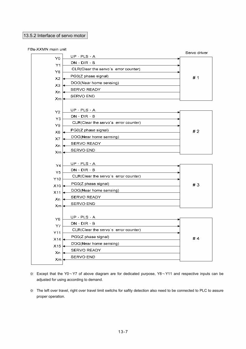
13-7
13.5.2 Interface of servo motor
※ Except that the Y0~Y7 of above diagram are for dedicated purpose, Y8~Y11 and respective inputs can be
adjusted for using according to demand.
※ The left over travel, right over travel limit switchs for safity detection also need to be connected to PLC to assure proper operation.

13-8
13.5.3 Working diagram illustration for servo motor
The Encoder of servo motor feedback the shifting detection signal to servo driver. The driver gets the pulse frequency, and pulse count of input signal (pulse command), as well as the frequency and pulse count of feedback signal processed with internal error counter and frequency to voltage conversion circuit, and acquired the pulse and turning speed deviations. Using these operations to control the servo motor, so as to obtain a high speed, precise speed and positional closed-loop processing system.
The revolving speed of servo motor depends on the pulse frequency of input signal; the turning stroke of motor is determined by pulse count.
Generally speaking, the final control error deviation of servo motor is ±1 pulse.
13.6 Explanation of function for NC position control instruction
The NC position control of FBs-PLC has following four related instructions:
FUN140 (HSPSO) high speed pulse output instruction, which includes following 8 extension positioning instructions:
1. SPD 5. ACT 2. DRV 6. EXT 3. DRVC 7. GOTO 4. WAIT 8. MEND
FUN141 (MPARA) positioning parameter setting instruction
FUN142 (PSOFF) enforcing pulse output stop instruction.
FUN143 (PSCNV) converting the current pulse value to displaying value instruction.
The following function explanations are for the above mentioned 4 instructions:
Used for positioning program coding and stored to SR operand area of FUN140

NC Positioning Control Instruction
13-9
FUN 140 HSPSO
High Speed Pulse Output (Including the extended positioning instruction)
FUN 140 HSPSO
Ps :ENExecution
control
Ladder symbol
140.HSPSOACT
ERRPause INC
Abort ABT
SR :
WR :
DN
Acting
Error
Done
Ps : The set number of Pulse Output (0~3) 0:Y0 & Y1 1:Y2 & Y3 2:Y4 & Y5 3:Y6 & Y7
SR: Starting register for positioning program (example explanation)
WR: Starting register for instruction operation (example explanation). It controls 7 registers, which the other program cannot repeat in using.
HR DR ROR K Range
Ope- rand
R0 ∣
R3839
D0 ∣
D3999
R5000∣
R8071
Ps 0~3SR WR *
Instruction Explanation
1. The NC positioning program of FUN140 (HSPSO) instruction is a program written and edited with text programming. We named every position point as a step (which includes output frequency, traveling distance, and transfer conditions). For one FUN140, it can be arranged with 250 steps of positioning points at the most, with every step of positioning point controlled by 9 registers.
2. The best benefit to store the positioning program into the registers is that in the case of association with MMI (Man Machine Interface) to operate settings, it may save and reload the positioning program via MMI when replacing the molds.
3. When execution control “EN”=1, if the other FUN140 instructions to control Ps0 ~ 3 are not active (corresponding status of Ps0=M1992, Ps1=M1993, Ps2=M1994, and Ps3=M1995 will be ON), it will start to execute from the next step of positioning point (when goes to the last step, it will be restarted from the first step to perform); if Ps0~3 is controlled by other FUN140 instruction (corresponding status of Ps0=M1992, Ps1=M1993, Ps2=M1994, and Ps3=M1995 would be OFF), this instruction will acquire the pulse output right of positioning control once the controlling FUN140 has released the control right.
4. When execution control input “EN” =0, it stops the pulse output immediately.
5. When output pause “PAU” =1 and execution control “EN” was 1 beforehand, it will pause the pulse output. When output pause “PAU” =0 and execution control is still 1, it will continue the unfinished pulse output.
6. When output abort “ABT”=1, it stops pulse output immediately. (When the execution control input “EN” becomes 1 next time, it will restart from the first step of positioning point to execute.)
7. While the pulse is in output transmitting, the output indication “ACT” is ON.
8. When there is execution error, the output indication “ERR” will be ON. (The error code is stored in the error code register.)
9. When each step of positioning point is complete, the output indication “DN” will be ON.

NC Positioning Control Instruction
13-10
FUN 140 HSPSO
High Speed Pulse Output (Including the extended positioning instruction)
FUN 140 HSPSO
*** The working mode of Pulse Output must be set (without setting, Y0~Y7 will be treated as general output) to be one of U/D, P/R, or A/B mode, thus the Pulse Output may have a regular output.
U/D Mode : Y0 (Y2, Y4, Y6), it sends out upward counting pulse. Y1 (Y3, Y5, Y7), it sends out downward counting pulse.
P/R Mode : Y0 (Y2, Y4, Y6), it sends the pulse out. Y1 (Y3, Y5, Y7), it sends out the directional signal; ON=upward counting, OFF= downward counting.
A/B Mode : Y0 (Y2, Y4, Y6), it sends out the phase A pulse. Y1 (Y3, Y5, Y7), it sends out the phase B pulse.
The output polarity for Pulse Output can select to be Normal ON or Normal OFF.
〔The interfaces for positioning control〕
ON : stop or pause FUN140, slow down and stop pulse output. M1991 OFF : stop or pause FUN140, stop pulse output immediately.
ON : Ps0 Ready M1992 OFF : Ps0 is in action
ON : Ps1 Ready M1993 OFF : Ps1 is in action
ON : Ps2 Ready M1994 OFF : Ps2 is in action
ON : Ps3 Ready M1995 OFF : Ps3 is in action
M1996 ON : Ps0 has finished the last step
M1997 ON : Ps1 has finished the last step
M1998 ON : Ps2 has finished the last step
M1999 ON : Ps3 has finished the last step
M2000 : ON, multi axes acting simultaneously (At the same scan, when execution control “EN”= 1of FUN140 instructions which control Ps0~3, their pulses output will be sent at the same time without any time lag).
: OFF, as the FUN140 for Ps0~3 starts, corresponding axis pulse output will be sent immediately; since the ladder program is executed in sequence, therefore even the FUN140 for Ps0~3 started at the same scan, there must be some time lag between them.
Ps No. Current output frequency
Current pulse position
The remaining pulse counts to be transmitted Error code
Ps0 DR4080 DR4088 DR4072 R4060 Ps1 DR4082 DR4090 DR4074 R4061 Ps2 DR4084 DR4092 DR4076 R4062 Ps3 DR4086 DR4094 DR4078 R4063
※ R4056 : When the value of low byte=5AH, it can be dynamically changed for its output frequency during the
high speed pulse output transmitting at any time.
When the value of low byte is not 5AH, it can not be dynamically changed for its output frequency during the high speed pulse output transmitting.
The default value of R4056 is 0

NC Positioning Control Instruction
13-11
FUN 140 HSPSO
High Speed Pulse Output (Including the extended positioning instruction)
FUN 140 HSPSO
R4064 : The step number (positioning point) which has been completed of Ps0.
R4065 : The step number (positioning point) which has been completed of Ps1.
R4066 : The step number (positioning point) which has been completed of Ps2.
R4067 : The step number (positioning point) which has been completed of Ps3.
Format of positioning program:
SR: Starting register of registers block which reserved to store positioning program, explained as follows:
SR A55AH The effective positioning program; its starting register must be A55AH
SR+1 Total steps 1~250
SR+2
SR+3
SR+4
SR+5
SR+6
SR+7
The first positioning point (step) of positioning program (every step controlled by 9 registers).
SR+8
SR+9
SR+10
The Nth step of positioning program.
SR+N×9+2

NC Positioning Control Instruction
13-12
FUN 140 HSPSO
High Speed Pulse Output (Including the extended positioning instruction)
FUN 140 HSPSO
Explanation for working register of instruction operation:
WR is the starting register.
WR+0 Being executed or stopped step
WR+1 Working flag
WR+2 Controlled by system
WR+3 Controlled by system
WR+4 Controlled by system
WR+5 Controlled by system
WR+6 Controlled by system
WR+0 : If this instruction is in execution, the content of this register represents the step (1~N) being performed. if this instruction is not in execution, the content of this register represents the step where it stopped at present When execution control “EN” =1, it will perform the next step, i.e. the current step plus 1 (if the current step is at the last step, it will restart to perform from the first step). Before starting the execution control “EN” =1, the user can renew the content of WR+0 to determine starting from which step to perform (when the content of WR+0 =0, and execution control “EN” =1, it represents that the execution starts from the first step).
WR+1 : B0~B7, total steps
B8 = ON, output paused
B9 = ON, waiting for transfer condition
B10 = ON, endless output (the stroke operand of DRV command is set to be 0 )
B12 = ON, pulse output transmitting (the status of output indicator “ACT”)
B13 = ON, instruction execution error (the status of output indicator “ERR”)
B14 = ON, finished being executed step (the status of output indicator “DN”)
*** Once the FUN140 instruction has been started (the B12 of WR+1=ON) and if suspended by a shut down for emergency or switchover from auto to manual mode while the pulse output has not yet completed, this instruction will be negated at next execution. It must clear the WR+1 register to be 0 before restarts the instruction next time, so as to make the instruction be initiated again; otherwise, the pulse output will not appear!
*** Whether execution control “EN” =0 or 1, executing the FUN140 instruction every scan , there won’t have the situation mentioned above.
*** When step which has been completed, the output indication “DN” will turn ON and keep such status if suspending ; the user may turn OFF the status of “DN” by using the rising edge of output coil controlled by "DN" to clear the content of WR+1 register to be 0, and it can be attained.

NC Positioning Control Instruction
13-13
FUN 140 HSPSO
High Speed Pulse Output (Including the extended positioning instruction)
FUN 140 HSPSO
Error indication Error code
R4060(Ps0) 0 : Error free
R4061(Ps1) 1 : Parameter 0 error
R4062(Ps2) 2 : Parameter 1 error
R4063(Ps3) 3 : Parameter 2 error
4 : Parameter 3 error
5 : Parameter 4 error
6 Parameter 5 error The possible error codes
7 : Parameter 6 error for FUN141 execution
8 : Parameter 7 error
9 : Parameter 8 error
10 : Parameter 9 error
13 Parameter 12 error
15 Parameter 14 error
30 : Error of variable address for speed setting
31 : Error of setting value for speed setting
32 : Error of variable address for stroke setting
33 : Error of setting value for stroke setting
34 : Illegal positioning program
35 : Length error of total step The possible error codes
36 : Over the maximum step for FUN140 execution
37 : Limited frequency error
38 : Initiate/stop frequency error
39 : Over range of compensation value for movement
40 : Over range of moving stroke
41 : ABS positioning is not allowed within DRVC commands
Note : The content of error indication register will keep the latest error code. Making sure that no more error to happen, you can clear the content of error indication register to be 0; as long as the content maintains at 0, it represents that there’s no error happened.
Editing Servo Program Table with WinProladder
Click the “Servo Program Table” Item which in project windows :
Project name
Table Edit
Servo Program Table Click right button and select “New Table”

NC Positioning Control Instruction
13-14
FUN 140 HSPSO
High Speed Pulse Output (Including the extended positioning instruction)
FUN 140 HSPSO
Table Type : It will be fixed to ” Servo Program Table ”. Table Name : For modify or debug, you can give a convenient name. Table Starting address : Enter the address which Starting register of Servo Program Table.

NC Positioning Control Instruction
13-15
FUN 140 HSPSO
High Speed Pulse Output (Including the extended positioning instruction)
FUN 140 HSPSO
For easy programming and trouble shooting, the WinProladder provides the text editing environment to edit the motion program(servo program table) for FUN140 execution; Key in the complete FUN140 instruction first and then move the cursor to the position of it, pressing the hot key ”Z”, then comes the text editing environment. The user can create the new motion program or display the existed program under this friendly user interface operation.
Extended positioning instructions are listed as follows:
Instruction Operand Explanation
SPD XXXXXX or Rxxxx or Dxxxx
Moving speed in frequency or velocity (FUN141 Parameter_0=0 represents velocity; Parameter_0=1 or 2 for frequency; the system default is frequency). The operand can be input directly with constant or variable (Rxxxx, Dxxxx); when the operand is variable, it needs 2 registers, e.g. D10 represents D10 (Low Word) and D11 (High Word), which is the setting of frequency or velocity.
When selecting to use the velocity setting, the system will automatically convert the velocity setting to corresponding output frequency.
Output frequency range: 1≦output frequency≦921600 Hz. *** When the output frequency is 0, this instruction will wait until
the setting value isn’t 0 to execute the positioning pulse output.
Moving stroke setting in Ps or mm,Deg,Inch (When FUN141 Parameter_0=1, the setting stroke in Ut is Ps; Parameter_0=0 or 2, the setting stroke in Ut is mm, Deg, Inch; the system default for Ut is Ps).
When 4_th operand of DRV is Ut (not Ps) , according to parameter setting of 1, 2, 3 of FUN141, the system will convert the corresponding pulse count to output.
There are 4 operands to construct DRV instruction as follows: 1_st operand: coordinate selection.
ADR or ABS: ADR, relative distance movement ABS, absolute position movement
2_nd operand: revolving direction selection (Valid for ADR only).
'+' , forward or clockwise '−' , backward or counterclockwise ' ' ,direction is determined by the setting value
(positive value: forward; negative value: backward) 3_rd operand: moving stroke setting
XXXXXXXX: or −XXXXXXXX or Rxxxx or Dxxxx
It can directly input with constant or variable (Rxxxx, Dxxxx); it needs 2 registers when adopting the variable, e.g. R0 represents R0 (Low Word) and R1 (High Word) as the setting of moving stroke.
DRV ADR ,+ ,XXXXXXXX,Ut ADR ,+ ,XXXXXXXX,Ps ADR ,− ,XXXXXXXX,Ut ADR ,− ,XXXXXXXX,Ps ADR , , XXXXXXXX,Ut ADR , ,−XXXXXXXX,Ut ADR , , XXXXXXXX,Ps ADR , ,−XXXXXXXX,Ps ADR ,+ ,Rxxxx,Ut ADR ,+ ,Rxxxx,Ps ADR ,− ,Rxxxx,Ut ADR ,− ,Rxxxx,Ps ADR , ,Rxxxx,Ut ADR , ,Rxxxx,Ps ADR ,+ ,Dxxxx,Ut ADR ,+ ,Dxxxx,Ps ADR ,− ,Dxxxx,Ut ADR ,− ,Dxxxx,Ps ADR , ,Dxxxx,Ut ADR , ,Dxxxx,Ps ABS , , XXXXXXXX,Ut ABS , ,−XXXXXXXX,Ut ABS , , XXXXXXXX,Ps ABS , ,−XXXXXXXX,Ps ABS , ,Rxxxx,Ut ABS , ,Rxxxx,Ps ABS , ,Dxxxx,Ut ABS , ,Dxxxx,Ps
*** When the setting of moving stroke is 0 and 1_st operand is ADR, it represents to revolve endless.
Stroke setting range: −99999999 ≤ stroke setting ≤ 99999999 4_th operand: resolution of stroke setting Ut or Ps:for Ut, the resolution is one unit; (it is determined by parameter 0, 3 of FUN141); for Ps, the enforced resolution is one pulse.

NC Positioning Control Instruction
13-16
FUN 140 HSPSO
High Speed Pulse Output (Including the extended positioning instruction)
FUN 140 HSPSO
Instruction Operand Explanation The usage of DRVC and the operand explanation is the same as DRV’s instruction. *** DRVC is used to do successive speed changing control (8 speeds
at the most). *** Of the successive speed changing control, only the first DRVC
instruction can use the absolute value coordinate for positioning. *** The revolution direction of DRVC can only be decided by ‘+’ or ‘−’. *** The revolution direction only determined by the first DRVC of
successive DRVC instructions; i.e. the successive speed changing control can only be the same direction.
For example: successive 3 speed changing control
001 SPD 10000 DRVC ADR,+,20000,UtGOTO NEXT
002 SPD 50000 DRVC ADR,+,60000,UtGOTO NEXT
003 SPD 3000 DRV ADR,+,5000,Ut WAIT X0 GOTO 1
* Pulse frequency = 10KHz. * Forward 20000 units.
* Pulse frequency =50 KHz * Forward 60000 units.
* Pulse frequency = 3KHz. * Forward 5000 units. * Wait until X0 ON to restart from
the first step to execute.
DRVC ADR,+,XXXXXXXX,Ut or or or or
ABS,−, Rxxxx ,Ps or
Dxxxx
Note: The number of DRVC instructions must be the number of successive speeds deducted by 1, i.e. the successive speed changing control must be ended with the DRV instruction.
The above mentioned example is for successive 3 speeds changing control, which used 2 DRVC instructions and the third must use DRV instruction.
Diagram illustration for the above mentioned example:
f2
f1f3
f
50000
100003000
Ut20000 60000 5000
Note: Comparison explanation between the relative coordinate positioning (ADR) and the absolute coordinate positioning (ABS)
To move from position 30000 to −10000, the coding for programming is: DRV ADR,−,40000,Ut or DRV ABS, ,−10000,Ut
... ...
-10000 0 10000 20000 30000 Ut
To move from position −10000 to 10000, the coding for programming is: DRV ADR,+,20000,Ut or DRV ABS, ,10000,Ut

NC Positioning Control Instruction
13-17
FUN 140 HSPSO
High Speed Pulse Output (Including the extended positioning instruction)
FUN 140 HSPSO
Instruction Operand Explanation
WAIT Time, XXXXX
or Rxxxx
or Dxxxx
or X0~X255
or Y0~Y255
or M0~M1911
or S0~S999
When pulse output is complete, performing the wait instruction for going to the next step. There are 5 kind of operands that explained as follows:
Time: The waiting time (the unit is 0.01 second), it can be directly input with constant or variable (Rxxxx or Dxxxx); when it is time up, performs the step that assigned by GOTO.
X0~X255: Waiting until the input status is ON, it performs the step that assigned by GOTO.
Y0~Y255:Waiting until the output status is ON, it performs the step that assigned by GOTO.
M0~M1911: Waiting until the internal relay is ON, it performs the step that assigned by GOTO.
S0~S999: Waiting until the step relay is ON, it performs the step that assigned by GOTO.
ACT Time,XXXXX or Rxxxx or Dxxxx
After the time to output pulses described by operand of ACT, it performs immediately the step that assigned by GOTO, i.e. after the pulse output for a certain time, it performs the next step immediately. The action time (the unit is 0.01 second) can be directly input with constant or variable (Rxxxx or Dxxxx); when the action time is up, it performs the step assigned by GOTO.
EXT X0~X255 or Y0~Y255 or M0~M1911 or S0~S999
External trigger instruction; when it is in pulse output (the number of pulses sending is not complete yet), if the status of external trigger is ON, it will perform the step assigned by GOTO immediately. If the status of external trigger is still OFF when the pulse output has been complete, it is the same as WAIT instruction; waiting the trigger signal ON, then perform the step assigned by GOTO.
GOTO NEXT or 1~N or Rxxxx or Dxxxx
When matching the transfer condition of WAIT, ACT, EXT instruction, by using GOTO instruction to describe the step to be executed.
NEXT: It represents to perform the next step. 1~N: To perform the described number of step. Rxxxx: The step to be performed is stored in register Rxxxx. Dxxxx: The step to be performed is stored in register Dxxxx.
MEND The end of the positioning program.

NC Positioning Control Instruction
13-18
FUN 140 HSPSO
High Speed Pulse Output (Including the extended positioning instruction)
FUN 140 HSPSO
The coding for positioning programming :
First,it must complete the FUN140 instruction before the editing of positioning program, and assigned in FUN140 instruction the starting register of registers block to store positioning program. While editing the positioning program, it will store the newly edited positioning program to the assigned registers block; for every one positioning point (called as one step) edited, it is controlled by 9 registers. If there are N positioning points, it will be controlled by N × 9 + 2 registers in total.
Note: The registers storing the positioning program can not be repeated in using!
Format and example for the positioning program 1:
001 SPD 5000 ; Pulse frequency = 5KHz. DRV ADR,+,10000,Ut ; Moving forward 10000 units. WAIT Time,100 ; Wait for 1 second. GOTO NEXT ; Perform the next step. 002 SPD R1000 ; Pulse frequency is stored in DR1000 (R1001 and R1000). DRV ADR,+,D100,Ut ; Moving forward,the stroke is stored in DD100 (D101 and D100). WAIT Time,R500 ; The waiting time is stored in R500. GOTO NEXT ; To perform the next step. 003 SPD R1002 ; Pulse frequency is stored in DR1002 (R1003 and R1002). DRV ADR,−,D102,Ut ; Moving backward,the stroke is stored in DD102 (D103 and D102). EXT X0 ; When external trigger X0 (slow down point) ON, it performs the next
GOTO NEXT ; step immediately. 004 SPD 2000 ; Pulse frequency = 2KHz. DRV ADR,−,R4072,Ps ; Keep outputing the remain (stored in DR4072). WAIT X1 : Wait until X1 ON, GOTO 1 : Perform the first step.
Format and example for the positioning program 2:
001 SPD R0 ; Pulse frequency is stored in DR0 (R1 & R0). DRV ABS, ,D0,Ut ; Move to the position stored in DD0 (D1 & D0). WAIT M0 ; Wait until M0 ON, GOTO NEXT ; Perform the next step. 002 SPD R2 ; Pulse frequency is stored in DR2 (R3 & R2). DRV ADR, ,D2,Ut ; Moving stroke is stored in DD2 (D3 & D2);working direction determined
; by the sign of setting value MEND ; End of positioning program

Example for FUN140 Program Application
13-19
Program example: Jog forward As the jog forward button has been pressed for less than 0.5 second (changeable), it sends out only one (changeable) pulse; As the jog forward button has been pressed for more than 0.5 second (changeable), it continuously sends pulses out (the frequency is 10KHz, changeable), until the release of the jog forward button to stop the pulse transmitting; or it may be designed to send N pulses out at the most.
Conditionfor action
M0 M1996
M0
Jog forward button
Jog forward button
Manualoperation
ServoReady
PsEN : 0 ACT
SETEN M1
WRPAU
ABT
SR
: R 2000
: R 5000::
ERR
DN
M1000140.HSPSO
RSTEN R2000
RSTEN M1
M0
M0
M1
M1001
M1002
• Clear finish signal.
• Perform from the first step every time.
• When the last step been complete, set finish signal.
Program example: Jog Backward As the jog backward button has been pressed for less than 0.5 second (changeable) it sends out only one (changeable) pulse; As the jog backward button has been pressed for more than 0.5 second (changeable), it continuously sends pulses out (the frequency is 10KHz, changeable), until the release of the jog backward button to stop the pulse transmitting; or it may be designed to send N pulses out at the most.
Conditionfor action
Jog forward button
Jog forward button
Manualoperation
ServoReady
PsEN : 0 ACT
SETEN
WRPAU
ABT
SR ::
ERR
DN
140.HSPSO
RSTEN
RSTEN M3
R2007
M2
M3 M2
M2
: R 5020
: R 2007
M1003
M1004
M1005
M2 M1996M3
• Clear finish signal. • Perform from the first step every time.
• When the last step been complete,
set finish signal.
Positioning Program: 001 SPD 1000
DRV ADR,+,1,Ps WAIT TIME,50 GOTO NEXT
002 SPD 10000 DRV ADR,+,999999,Ut MEND
Positioning Program: 001 SPD 1000
DRV ADR,−,1,Ps WAIT TIME,50 GOTO NEXT
002 SPD 10000 DRV ADR,−,999999,Ut MEND

NC Positioning Instruction
13-20
FUN 141 MPARA
Instruction of Parameter Setting for Positioning Program FUN 141 MPARA
Ps: The set number of Pulse Output (0~3). SR: Starting register for parameter table, it has totally 18
parameters which controlled by 24 registers.
HR DR ROR KRange
Ope- rand
R0 ∣
R3839
D0 ∣
D3999
R5000∣
R8071
Ps 0~3SR
Instruction explanation
1.This instruction is not necessary if the system default for parameter value is matching what users need. However, if it needs to open the parameter value to do dynamic modification, this instruction is required.
2.This instruction incorporates with FUN140 for positioning control purpose, each axis can have one FUN141 instruction only.
3. Whether the execution control input “EN” = 0 or 1, anyway, this instruction will be performed.
4. When there is error in parameter value, the output indication “ERR” will be ON, and the error code is appeared in the error code register.
Explanation for the parameter table: SR =Starting register of parameter table, suppose it is R2000.
R2000 (SR+0) 0~2 Parameter 0 System default =1 R2001 (SR+1) 1~65535 Ps/Rev Parameter 1 System default =2000
DR2002 (SR+2) 1~999999 µM/Rev 1~999999 mDeg/Rev 1~999999×0.1 mInch/Rev
Parameter 2 System default =2000
R2004 (SR+4) 0~3 Parameter 3 System default =2
DR2005 (SR+5) 1~921600 Ps/Sec 1~153000
Parameter 4 System default =512000
DR2007 (SR+7) 0~921600 Ps/Sec Parameter 5 System default =141 R2009 (SR+9) Reserved Parameter 6 System default =0 R2010 (SR+10) 0~32767 Parameter 7 System default =0
R2011 (SR+11) 0~30000 Parameter 8 System default =5000 R2012 (SR+12) 0~1 Parameter 9 System default =0 R2013 (SR+13) -32768~32767 Parameter 10 System default =0 R2014 (SR+14) -32768~32767 Parameter 11 System default =0 R2015 (SR+15) 0~30000 Parameter 12 System default =0 R2016 (SR+16) Reserved Parameter 13 System default =1 DR2017 (SR+17) 0~4294967295 Parameter 14 System default =0 DR2019 (SR+19) Reserved Parameter 15 System default =20000 DR2021 (SR+21) Reserved Parameter 16 System default =1000 R2023 (SR+23) Reserved Parameter 17 System default =10

NC Positioning Instruction
13-21
FUN 141 MPARA
Instruction of Parameter Setting for Positioning Program FUN 141 MPARA
Editing Servo Parameter Table with WinProladder
Click the “Servo Parameter Table” Item which in project windows :
Project name
Table Edit
Servo Parameter Table Click right button and select “New Table”
Table Type : It will be fixed to ” Servo Parameter Table ”.
Table Name : For modify or debug, you can give a convenient name.
Table Starting address : Enter the address which Starting register of Servo Parameter Table.
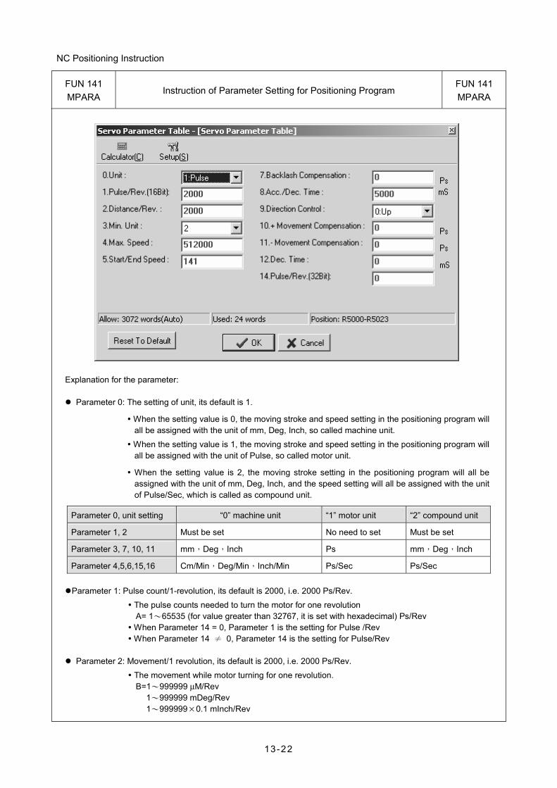
NC Positioning Instruction
13-22
FUN 141 MPARA
Instruction of Parameter Setting for Positioning Program FUN 141 MPARA
Explanation for the parameter:
Parameter 0: The setting of unit, its default is 1.
When the setting value is 0, the moving stroke and speed setting in the positioning program will all be assigned with the unit of mm, Deg, Inch, so called machine unit.
When the setting value is 1, the moving stroke and speed setting in the positioning program will all be assigned with the unit of Pulse, so called motor unit.
When the setting value is 2, the moving stroke setting in the positioning program will all be assigned with the unit of mm, Deg, Inch, and the speed setting will all be assigned with the unit of Pulse/Sec, which is called as compound unit.
Parameter 0, unit setting “0” machine unit “1” motor unit “2” compound unit
Parameter 1, 2 Must be set No need to set Must be set
Parameter 3, 7, 10, 11 mm,Deg,Inch Ps mm,Deg,Inch
Parameter 4,5,6,15,16 Cm/Min,Deg/Min,Inch/Min Ps/Sec Ps/Sec
Parameter 1: Pulse count/1-revolution, its default is 2000, i.e. 2000 Ps/Rev.
The pulse counts needed to turn the motor for one revolution A= 1~65535 (for value greater than 32767, it is set with hexadecimal) Ps/Rev
When Parameter 14 = 0, Parameter 1 is the setting for Pulse /Rev When Parameter 14 ≠ 0, Parameter 14 is the setting for Pulse/Rev
Parameter 2: Movement/1 revolution, its default is 2000, i.e. 2000 Ps/Rev.
The movement while motor turning for one revolution. B=1~999999 µM/Rev
1~999999 mDeg/Rev 1~999999×0.1 mInch/Rev

NC Positioning Instruction
13-23
FUN 141 MPARA
Instruction of Parameter Setting for Positioning Program FUN 141 MPARA
Parameter 3: The resolution of moving stroke setting, its default is 2.
Set value=0, machine unit; Set value=2, compound unit; Parameter 0
Parameter 3 mm Deg Inch Set value=1
motor unit (Ps)
Set value =0 ×1 ×1 ×0.1 ×1000
Set value =1 ×0.1 ×0.1 ×0.01 ×100
Set value =2 ×0.01 ×0.01 ×0.001 ×10
Set value =3 ×0.001 ×0.001 ×0.0001 ×1
Parameter 4: The limited speed setting, its default is 460000, i.e. 460000 Ps/Sec.
Motor and compound unit: 1~921600 Ps/Sec. Machine unit: 1~153000 (cm/Min, ×10 Deg/Min, Inch/Min).
However, the limited frequency can’t be greater than921600 Ps/Sec. f_max =(V_max ×1000×A)/(6×B)≤ 921600 Ps/Sec f_min ≥ 1 Ps/Sec
Note: A = Parameter 1, B =Parameter 2.
Parameter 5: Initiate/Stop speed, the default = 141. Motor and compound unit: 1~921600 Ps/Sec. Machine unit: 1~15300 (cm/Min, ×10 Deg/Min, Inch/Min).
However, the limited frequency can’t be greater than 921600 Ps/Sec.
Parameter 6: Reserved, the default = 0.
Parameter 7: Backlash compensation, the default =0.
Setting range: 0~32767 Ps. While backward traveling, the traveling distance will be added with this value automatically.
Parameter 8: Acceleration/Deceleration time setting, the default = 5000, and the unit is mS.
Setting range: 0~30000 mS. The setting value represents the time required to accelerate from idle state upto limited speed state or declerate from the limited speed state down to the idle state.
The acceleration/deceleration is constant slope depending on Parameter 4 / Parameter 8 When Parameter 12 = 0, Parameter 8 is the deceleration time There will have the auto deceleration function for short stroke movement.
Parameter 9: Coordinnate direction setting, the default =0.
Setting value =0, while in forward pulse output, the current Ps value is adding up. While in backward pulse output, the current Ps value is deducting down.
Setting value =1, while in forward pulse output, the current Ps value is deducting down. While in backward pulse output, the current Ps value is adding up.

NC Positioning Instruction
13-24
FUN 141 MPARA
Instruction of Parameter Setting for Positioning Program FUN 141 MPARA
Parameter 10: Forward movement compensation, the default = 0.
Setting range: −32768~32767 Ps. When it is in forward pulse output, it will automatically add with this value as the moving distance.
Parameter 11: Backward movement compensation, the default =0.
Setting range: −32768~32767 Ps. When it is in backward pulse output, it will automatically add with this value as the moving distance.
Parameter 12: Deceleration time setting, the default =0, and the unit is mS. Setting range: 0~30000 mS. When Parameter 12 = 0, Parameter 8 is the deceleration time When Parameter 12 ≠ 0, Parameter 12 is the deceleration time
Parameter 13: Reserved.
Parameter 14: Pulse count/1-revolution, the default = 0. The pulse counts needed to turn the motor for one revolution When Parameter 14 = 0, Parameter 1 is the setting for Pulse /Rev
When Parameter 14 ≠ 0, Parameter 14 is the setting for Pulse/Rev
Parameter 15: Reserved, it is recommended to be used as return home speed, the default = 20000 Ps/Sec.
Parameter 16: Reserved, it is recommended to be used as slow down speed while returning home , the default = 1000 Ps/Sec.
Parameter 17: Reserved.
Work speed
Parameter 5Initiate/Stop speed
Speed
Time
Parameter 4 : Max. speed
Work speed
Parameter 8or
Parameter 12
Parameter 8Acceleration/Deceleration
time setting

NC Positioning Instruction
13-25
FUN 142 P PSOFF
Enforcing to Stop Pulse Output FUN 142 P
PSOFF
Ladder symbol
142P.ENExecution control PSOFF Ps
N: 0~3, enforces the asigned set number of Pulse Output to stop its output.
Instruction Explanation
1. When stop control “EN” =1, or changes from 0→1( P instruction), this instruction will enforce the assigned set number of Pulse Output to stop its output.
2. When applying in the process of return home , as the home has returned, it can immediately stop the pulse output by using this instruction, so as to make it stop at the same position every time when performing machine homing.
Program example
142P.EN PSOFF 0
M0
; When M0 changes from 0→1, it enforces the Ps0 to stop the pulse output.

NC Positioning Instruction
13-26
FUN 143 P PSCNV
Converting the Current Pulse Value to the Displaying Value (mm, Deg, Inch, PS)
FUN 143 PPSCNV
Ps: 0~3; converting the asigned pulse position to mm (Deg, Inch, PS) which has the same unit as the set point, so as to make the current position displayed.
D: Registers that store the current position after conversion. It uses 2 registers, e.g. D10 represents D10 (Low Word) and D11 (High Word) two registers.
HR DR ROR KRange
Ope- rand
R0 ∣
R3839
D0 ∣
D3999
R5000∣
R8071
Ps 0~3D *
Instruction Explanation
1. When execution control “EN” =1 or changes from 0→1( P instruction), this instruction will convert the assigned current pulse position (PS) to be the mm (or Deg, Inch, or PS) that has the same unit as the set value, so as to make current position displaying.
2. After the FUN140 instruction has been performed, it will then be able to get the correct conversion value by executing this instruction.
Program Example
; When M0=1, it converts the current pulse position of Ps0 (DR4088) to the mm (or Deg or Inch or PS) that has the same unit as the set value, and store it into the DD10 to make the current position displaying.

13-27
13.7 Machine homing
The machine set which undertakes relative model Encoder as shifting detector usually need the reset action for the reference of positioning coordinate; we called this action as machine homing (seeking for zero reference).
The machine homing diagram for NC servo unit is as follows:
Method 1: Return home speed
Slow down speed
Left over travel limit switch Near home sensing Right over travel limit switch
When it encounters the near home signal, starts the Z phase counting.
Z phase counting is up, the pulse output stops, then send out the CLR signal to clear the error counter of servo driver.
e.g.: X3: Near home sensing input is configured as interrupt input; in the case of machine homing, it starts HSC4 to
begin counting in X3+ interrupt service subroutine. X2: Z phase counting input, it is configured as UP input of HSC4; the X2+ is prohibited to interrupt in regular time,
when executing machine homing and X3 near home interrupt occurred, it starts HSC4 to begin Z phase counting. When HSC4 counting is up, it stops the pulse output, prohibit the X2+ interrupt, set home position to signal, and sends out the CLR signal to clear the error counter of servo driver. Please consult program example.
Method 2: According to application demand, it may slow down when encountering the near home sensor, while over the sensor a little far away, stop the pulse output, and then traveling slowly with backward direction; the very moment when it get out of near home sensor (the sensing signal changes from 1→0), it is treated as machine home. This program is simpler!
Near home signal 1→0, machine zero reference
Left over travel limit switch Near home sensing Right over travel limit switch
X3: Near home sensing input; it is configured as falling edge interrupt input.
• Once encountering the near home sensor, it will enable X3 falling edge interrupt, and slow down to stop within the near home sensing range.
• Slowly backward traveling until the near home sensing signal changes from 1→0.
• When the near home sensing signal changes from 1→0, it performs the X3- interrupt service subroutine immediately.
• The X3- interrupt service subroutine: Stops the pulse output immediately, prohibits the X3- interrupt, sets home position to signal, and sends out CLR signal to clear the error counter of servo driver. (Please consult the example program.)
(2) Slow down speed
(3) Stop
(5) Stop
(1) Home speed
(4) Slowly backward

13-28
Program Example 1: Machine homing (method 1)
X2: Configured as the UP input of HSC4, and connected to Z phase input. X3: Configured as the rising edge interrupt input, and connected to near home sensing input.
【Main Program】
T0
Y8
M4
M51
M50
M1996
M4
M4
M92Manual
operationReadyServo
M5
M92
M1924
: R 4114D
: R 4088D
RST
.01S
EN
EN T0
Y8
50 TUP
M1007
M1006
ABT DN
: 008D.MOV
EN S
EN SET M5
140.HSPSO
PAU WR
EN Ps
SR
M1007M50
: R 2014
: 0
: R 5040::
ERR
ACT
M51
M4
D
: R 292308.MOV
RST
RST
RST
EN S
EN
D
EN
EN
R 4115
R 4112
R 2014
RST
RST
: R 2900
EN
EN RST
EN
SR
M1007
M5
M50
: 0141.MPARA
EN Ps
EN DIS146
X2+I
ERR
• Prohibits X2+ interruption (HSC4 does not count)
• Parameter table R2900→R2923.
• Clears the homing completion signal.
• Clears the instruction completion signal for homing
• Clears the error signal.
• Clears the step pointer, it starts from the first step to execute.
• Clears the current value of HSC4.
• Clears the High Word of preset value for HSC4.
• Fill the prset value of HSC4 with the content of Parameter 17 of FUN141.
• Configure R5000~R5199 as the read only register (ROR) before programming, after then, when storing program, the Ladder program will automatically contains the positioning program.
• Homing instruction completed
• Signal for homing completion
• Fill the current PS registers with 0, while homing completed.
• Signal to clear error counter of servo driver -- Y8 is ON for 0.5 second.
Positioning program: 001 SPD R2919
DRV ADR,−,999999,Ut EXT X3 GOTO NEXT
002 SPD R2921 DRV ADR,−,9999,Ut MEND

13-29
【Sub Program】
M4
M4
N : 169
ENEN X2+I
RTI
69
LBL
D74.IMDIO
EN
HSC4I
: Y8
RTI
PSOFF
DISEN
EN
X2+I
0
65LBL
145
Y8
M50
65
142
146
X3+I
• X3 rising edge interrupt service subroutine.
• Enables HSC4 counting if homing.
• Interrupt service subroutine of HSC4 (Z phase counting is up)
• Stops pulse output immediately.
• Prohibits rising edge interrupt of X2.
• Output to clear error counter of servo driver.
• Sets the homing completion signal.
• Sends output immediately.

13-30
Program Example 2: Machine homing (method 2)
X3: Connected to near home sensing input, and configured as falling edge interrupt input.
【Main Program】
Left overtravel limit
HOME
T0
M4
M50
M51
Y8
M1996
M4
M4
M20
M4
X3
ReadyServo
M5
Homing
M20
ManualoperationReady
Servo
M1924
65LBL
ACT: 0EN Ps
RST
: 008D.MOV
: R 4088EN S
D
EN Y8
.01S
EN T0
EN SET
SETEN
30
Y8
TUP
M5
PAU WR
ABT
SR: R 2014
: R 5040::
ERR
DN
M51
M1006
145P
RST
140.HSPSO
↑ ENEN
M50
EN
X3 - I
R2014
RST
EN
D
RST
EN M50
M5
M4
M20
CALLEN
67INIT
• Clears the homing completion signal.
• Clears the instruction completion signal for homing.
• Clears the step pointer, it starts from the first step to execute.
• Enable X3− (falling edge) interrupt.
• Configure R5000~R5199 to be the read only register (ROR) before programming, after then, when storing program, the Ladder program will automatically contains the positioning program.
• Homing instruction completed.
• Signal for homing completion.
• Output to clear error counter of servo driver -- Y8 is ON for 0.3 second.
• Fill the current PS registers with 0.
Positioning Program: 001 SPD R2919
DRV ADR,−,999999,Ut EXT X3 GOTO NEXT
002 SPD 1000 DRV ADR,−,1000,Ps WAIT TIME,10 GOTO NEXT
003 SPD R200 DRV ADR,+,999999,Ut MEND

13-31
【Sub Program】
69RTI
M4
LBL65
X3 - I
68RTS
65LBL INIT
EN DIS146
X3 - I
: 2900
141.MPARA: 0
PSOFFEN
142
SREN Ps
0
ERR
EN DIS146
X3 - I • Prohibits X3− interrupt
• Parameter table R2900~R2923
X3 falling edge interrupt service subroutine.
• Stops pulse output immediately
• Prohibits X3− interrupt
• Sets the homing completion signal.

13-32
Program Example 3: JOG Forward
M0 M1996
M0
↑
ServoReady
Manauloperation
Jog forward button
DNABT
SETEN M1
SR
Ps
WR
140.HSPSO
PAU
EN: R 5000
: R 2000
: 0
::
ERR
ACTM1000
M0
RSTEN M1
Jog forward button
EN RSTD
R 2000
M0
M1
M1001
• Clears the completion signal
• Starts from the first step every jog execution.
• As the execution of last step completed, it sets up the completion signal.
Program Example 4: JOG Backward
M2 M1996
M2
↑
DNABT
SETEN M3
SR
Ps
WR
140.HSPSO
PAU
EN: R 5020
: R 2007
: 0
::
ERR
ACTM1003
M2
RSTEN M3
EN RSTD
R 2007
M2
M3
M1004
Jog backward
buttonManaul
operationServoReady
Jog backward button
• Clears the completion signal.
• Starts from the first step every jog execution.
• As the execution of the last step completed, it sets up the completion signal.
Positioning program: 001 SPD 1000
DRV ADR,+,1,Ps WAIT TIME,50 GOTO NEXT
002 SPD R2907 DRV ADR,+,99999999,Ut MEND
Positioning Program 001 SPD 1000
DRV ADR,−,1,Ps WAIT TIME,50 GOTO NEXT
002 SPD R2907 DRV ADR,−,99999999,Ut MEND

13-33
Program Example 5: Step by step, One cycle, Continuous positioning control.
M93 : Start
M101 : Step by step operation mode
M102 : One cycle operation mode
M103 : Continuous operation mode
M104 : Regular shut down. M105 : Emergency stop.
M93
M6
M6↑
SERVOREADY
M93↑
DNABT
SR
Ps
WR
140.HSPSO
PAU
EN
M105 M1010
: R 5100
: R 2021
: 0
::
ERR
ACTM1009
M1010
M6
RST
RSTEN
EN
R 2022
R 2021
RST
RST
RST
EN
EN
EN
M1011
M1010
M7
M101
M101 M7
M1011M101
M1011
M1996
M103 M104
M6 M102M7EN SET
• Clears shut down signal.
• Clears the error signal.
• Clears the step completion signal.
• Except step by step mode, the step pointer is cleared to be 0; it starts from the first step to execute.
• Clears being active bit of FUN140
• Set up the shut down signal.
Positioning program: 001 SPD 1000
DRV ADR,+,20000,Ut WAIT TIME,100 GOTO NEXT
002 SPD 20000 DRV ADR,+,40000,Ut WAIT M200 GOTO NEXT
003 SPD 25000 DRV ADR,−,50000,Ut WAIT TIME,500 GOTO NEXT
004 SPD 5000 DRV ADR,−,10000,Ut WAIT X16 GOTO 1

MEMO

14-1
Chapter 14 Application of ASCII Output Function
The FBs-PLC's ASCII file output function allows the PLC to directly drive ASCII output devices such as printers and terminals, and let them print or display English document data or display screens such as production reports, materials details and warning messages. For application of the ASCII file output function, it is necessary to edit, the ASCII file data to be output must be edited to fit the required format of the FBs-PLC FUN 94 (ASCWR) instruction. Then using this instruction, it will be sent out via port 1 to the ASCII output device connected with port 1.
14.1 Format of ASCII file
ASCII file data may be divided into fixed, unchanging background file data and dynamically changing variable data. The background file data may be in English characters, numerals, symbols, graphs, etc, and the variable data can only be printed out as binary, decimal, or hexadecimal numeric value data.
ASCII code is a byte length code, which has a total of 256 combinations. Of these, the first 128 (0-127) are fairly clearly defined and are used by most of the ASCII peripherals. For codes greater than 128 each manufacturer has different definitions and graphics and there are no uniform specifications. FBs-PLC designed the FUN 94 (ASCWR) instruction to be solely responsible for transmission, and not for editing. This work is done by the ASCII editor of the WinProladder software package. Below is the editing command format adopted by the WinProladder software package editor.
1. Basic command Symbols
/ Linefeed
A line slanting down from right to left means that no matter where the printing is up to, if this symbol is encountered, then the printing head or the terminal display will move to the beginning (the very left) of the next line and go on printing or displaying from that point. A series of "/" will create a succession of linefeeds (one "/" will cause one linefeed) .
\ Pagefeed
A line slanting down from left to right means that when this symbol is encountered the printing head or the terminal display will move to the beginning (top left hand corner) of the next page, and continue printing or displaying from that point. A series of "\" will create a succession of pagefeeds. (One "\" will cause one pagefeed).
, Comma
Used to separate statements in the file data. All the data included between two commas is a complete and executable statement (must not be used for beginning and end of file). Note that although the shape of a comma is the same as the shape of a single quotation mark, their positions are different (the comma is in a position near the center of the letter, while the single quotation mark is near the top right corner). The function meaning that they represent is completely different. Please refer to Item 2, background data format - statements.
END File end
At the end of the ASCII file END is added to show that the ASCII file is finished.

14-2
2. Background Data Format
,M X N N1 N N2………, Repeat ASCII code(N)
or ,M X ' A B C D E F G H I J K ',
Repeat tangible ASCII code
MX: Represents the number of repeats. M can be 1 to 999. The ASCWR instruction can send out M times successively all the hexadecimal ASCII code or tangible ASCII code data contained between X and the first comma ( , ). If there is no data after X (ie, the comma comes directly after X), then the ASCWR instruction will send out M successive space codes. If you only have to send out the ASCII code or the tangible ASCII code once, then MX can be discarded.
ASCII code data format: This data format has an N two-digit hexadecimal value. Every two adjoining hexadecimal numerals starting from the right hand side of X will be regarded as an ASCII code. NN can be any ASCII code, including tangible or intangible ASCII code such as English characters, numeric symbols or control codes. However, its main use is as a special tangible code for control codes which cannot be represented by tangible character fonts or cannot find a font or symbol on the WinProladder ASCII editor. For tangible characters or symbols that can be directly represented on the ASCII editor by tangible keys, it should be more convenient to use the original printing out format. For example, if you want to print out the character "A", with the original printing method you can type A via the keyboard. But if you want to use ASCII code, you must check the table on which "A" is represented by 41 H, and then enter 41. It is obviously a lot less convenient.
Original printing out tangible ASCII code data format: What is enclosed within two single quotation marks' ', can only be tangible ASCII code such as English characters, numerals, symbols, and graphics (characters that can be found on or input via the ASCII editor keyboard). The ASCWR instruction will faithfully print out all the characters that are contained in ' ', so if you need to print out a single quotation mark itself, you must have two successive single quotation marks. For example:
'I''M A BOY' will be printed out as I' M A BOY
If the graphics or symbols of the ASCII output device cannot be found on the ASCII editor keyboard, then you naturally are unable to do input using this format. In such a case you can check the ASCII code for that symbol or graphic, and use ASCII code to input and print out.
3. Variable Data Format
,"8 . 2 R 0 D",
format code variable register digits after the decimal point
total number of variables printed out
A data statement within two double quotation marks " ", is used to specify the register address of variable data, and what format or format code it will be printed out .
Total number of variables printed out: In this example, "8" are used to print out the reserved 8 digit columns of the variable (R0) numeric value (including negative signs). If the variable value is larger than the total number of printed out digits then the high digit will be cut out. If the number of digits is insufficient, the remaining positions will be occupied by spaces.
Digits after the decimal point: The number of digits after the decimal point within the total number of digits of the variable. In this example, in a total number of 8 digits, there are 2 places after the decimal point. The decimal point symbol "." itself occupies one position so the integer will remain 5 digits.

14-3
Variable register: Can be R, D,WX, WY,etc, of a 16-bit register, or DR,DD,DWX, DWY, etc, of a 32-bit register. The contents of these registers can be retrieved and printed out using the format and format code specified by the contents of " " .
Format code: Can use hexadecimal H, decimal D or binary B format for printing out (when format code is not specified, it will be decimal - therefore D can be omitted).
This example assumes that the content value of R0 is -32768. In the 8.2 format, the print out result is
−3 2 7 . 6 8
If the format changes from 8.2 to 5.1 then the print out result changes to
2 7 6 . 8
14.2 Application examples of ASCII file output
The file data print out will start from the top left hand corner of each page. It will print from left to right with lines going from top to bottom (please refer to the format in the diagram below). When the final character in a line is reached (this varies according to the output device - a printer can have 80 characters or 132 characters), the printer will automatically jump to the start (left-hand side) of the next line. If it has not yet printed to the final character, but encounters the linefeed command (/) or the page feed command (\), then it will jump to the start of the next line or the next page, and start printing from that point.
Suppose that the production statistics table for the manufacturing division of a certain company has the following format. This can be used as an example to explain the editing and printing out of its ASCII file data.
↓
← ...................28 spaces.....................→ PRODUCTION REPORT ==================
← ................................ 52 spaces .......................................................................................→DATE: 1/20/99
←... .16 spaces.. .. → TOTAL NUMBER (A): 1000 PCS
NUMBER OF YIELD (B): 983 PCS
NUMBER OF REPAIR (C): 17 PCS
STANDARD TIME (D): 8.5 MIN/PCS
TOTAL WORKING TIME (E): 8500 MIN
ACTUAL WORKING TIME (F): 9190 MIN
EFFICIENCY (G): 92.49 %
←… … … 22 spaces… … … →REMARK: A×D=E,E/F=G
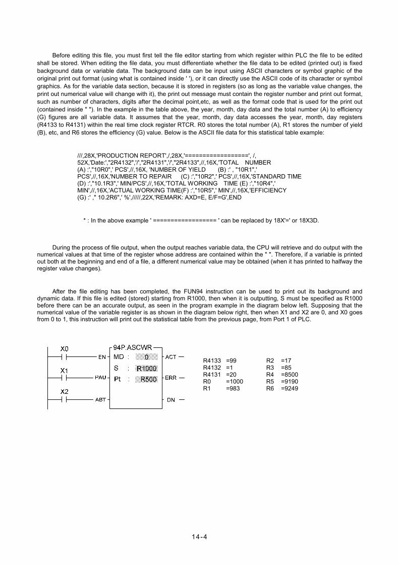
14-4
Before editing this file, you must first tell the file editor starting from which register within PLC the file to be edited shall be stored. When editing the file data, you must differentiate whether the file data to be edited (printed out) is fixed background data or variable data. The background data can be input using ASCII characters or symbol graphic of the original print out format (using what is contained inside ' '), or it can directly use the ASCII code of its character or symbol graphics. As for the variable data section, because it is stored in registers (so as long as the variable value changes, the print out numerical value will change with it), the print out message must contain the register number and print out format, such as number of characters, digits after the decimal point,etc, as well as the format code that is used for the print out (contained inside " "). In the example in the table above, the year, month, day data and the total number (A) to efficiency (G) figures are all variable data. It assumes that the year, month, day data accesses the year, month, day registers (R4133 to R4131) within the real time clock register RTCR. R0 stores the total number (A), R1 stores the number of yield (B), etc, and R6 stores the efficiency (G) value. Below is the ASCII file data for this statistical table example:
///,28X,'PRODUCTION REPORT',/,28X,'==================', /, 52X,'Date:',"2R4132",'/',"2R4131",'/',"2R4133",//,16X,'TOTAL NUMBER (A) :',"10R0",' PCS',//,16X, 'NUMBER OF YIELD (B) :' , "10R1",' PCS',//,16X,'NUMBER TO REPAIR (C) :',"10R2",' PCS',//,16X,'STANDARD TIME (D) :',"10.1R3",' MIN/PCS',//,16X,'TOTAL WORKING TIME (E) :',"10R4",' MIN',//,16X,'ACTUAL WORKING TIME(F) :',"10R5",' MIN',//,16X,'EFFICIENCY (G) :' ," 10.2R6",' %',/////,22X,'REMARK: AXD=E, E/F=G',END
* : In the above example ' ================== ' can be replaced by 18X'=' or 18X3D.
During the process of file output, when the output reaches variable data, the CPU will retrieve and do output with the numerical values at that time of the register whose address are contained within the " ". Therefore, if a variable is printed out both at the beginning and end of a file, a different numerical value may be obtained (when it has printed to halfway the register value changes).
After the file editing has been completed, the FUN94 instruction can be used to print out its background and dynamic data. If this file is edited (stored) starting from R1000, then when it is outputting, S must be specified as R1000 before there can be an accurate output, as seen in the program example in the diagram below left. Supposing that the numerical value of the variable register is as shown in the diagram below right, then when X1 and X2 are 0, and X0 goes from 0 to 1, this instruction will print out the statistical table from the previous page, from Port 1 of PLC.
R4133 =99 R2 =17 R4132 =1 R3 =85 R4131 =20 R4 =8500 R0 =1000 R5 =9190 R1 =983 R6 =9249

15-1
Chapter 15 Real Time Clock (RTC)
A real time clock (RTC) has been built in the FBs-PLC's MC/MN main unit. No matter whether the PLC is switched on or off, the RTC will always keep accurate time. It provides 7 kinds of time value data-week, year, month, day, hour, minute and second. Users can take advantage of the real time clock to do 24 hour controls throughout the year (for example, businesses or factories can switch lights on and off at set times each day, control gate access, and do pre-cooling and pre-heating before business or operations begin). It can enable your control system to automatically coordinate with people's living schedules, and not only will it raise the level of automatic control, it will improve efficiency.
15.1 Correspondence between RTC and the RTCR within PLC
Within PLC, there are special purpose registers (RTCR) for storing the time values of the RTC. There are 8 RTCR registers in all, going from R4128 to R4135. R4128 to R4134 are used to store the 7 kinds of time values mentioned above, from weeks to seconds. Because in practical daily application, certain hour and minute time data is often used, we have specially merged the time values of the hour register (R4130) and minute register (R4129) within RTCR, and put them in R4135 high byte and low byte, so they can be accessed by the user. The diagram below shows the correspondence between RTC and the RTCR within PLC, as well as the control switch and status flag (M1952-M1955) related to RTC accessing.

15-2
15.2 RTC access control and setting
Within PLC, the RTCR registers have been allocated to store the time values of RTC, and this is of great convenience to the user. However, if you want to load the set values of RTCR into RTC or read out what is in RTC onto RTCR, and tune the time value etc, then the setting must be done using the special relays (M1952 and M1953) for RTC access. Below is an explanation of the access and adjustment procedures, and the status flag relays.
1. RTC setting: The (RTCR→RTC) setting action is only executed once at the moment that relay M1952 goes from 1→0 (falling edge).
ON
M1952 Timing stopped Timing active
At the moment when M1952 goes from 1 to 0, the set values of R4128 to R4134 within RTCR will be written into the corresponding hardware registers within RTC. After M1952 has returned to 0 the timing action will start. Also, with each scan, CPU will retrieve time values from RTC in the opposite direction and write them onto RTCR.
Note: If you want to load the set values into RTC, you must first make M1952 as 1 and then load the set values into RTCR. The loading of the set values into RTCR can be done via MOVE instruction. However, you must first halt the RTC read out (make M1952 as 1), otherwise the data that you just wrote into RTCR will immediately be overridden by the time data being read back from RTC in the opposite direction.
2. RTC read out (RTC→RTCR): whenever the M1952 relay is 0 (RTC timing active). With every scan, CPU will take the time value data within RTC and move it to RTCR. When it is 1, it will not read out. In this case RTCR can load in the set values and they won't be overridden.
3. ±30 second adjustment: At the moment that the status of relay M1953 goes 1, CPU will check the value of the second register (R4128) within RTC. If its value is between 0 and 29 seconds then it will be cleared to 0. If its value is between 30 and 59 seconds then besides being cleared to 0, the minute register (R4129) will be increased by 1 (ie, one minute will be added). This can be used to adjust your RTC time value.
4. M1954 RTC installation detecting flag: When RTC is fitted to the PLC, relay M1954 will be set as 1; otherwise it will be 0.
5. M1955 set value error flag: When the time value which is set to RTC's IC is illegal, then the error flag relay M1955 will be set as 1, and the setting action will not be executed.

15-3
Setting calendar with WinProladder
Click the “calendar” Item which in Tool bar :
PLC
Setting
calendar Click right button and select “New Table”
『 PLC current time 』 : It is means current time of PLC in on-line situation. In the “Setup” frame, if “Apply PC time” item is chosen then current time of PC will display below, press “Update PLC time” button to write PC’s current time into PLC. But if “Apply PC time” item isn’t chosen you can modify the Date and Time by yourself. After you change the Date and Time, press “Update PLC time” button to write the Date and time into PLC’s calendar.

MEMO

16-1
Chapter 16 FBs-7SG 7/16-segment LED Display Module 16.1 FBs-7SG overview
There two models in the FBs-7SG range: 7SG1 and 7SG2. Each of which has one or two 8-digit display driver ICs for driving eight or sixteen 7-segment LED displays using a common ground; or four or eight 16-segment LED displays. The drawing below is an example of FBs-7SG2. Appearance
External 24V power input
Expansion output(connect to lower level expansion unit)
Expansion input(connect to main unit or upper level expansion unit)
CH1
POWPOW
CH0
0POW 1
FATEK
EXT VO
VO
2nd set
First set
FBs-7SG has been equipped with an exclusive 7-segment LED display driver IC for multiplexing display of one to eight 7-segment or one to four 16-segment LED displays (one group). With one 16-core flat ribbon cable, users can display 8 digits (numbers) or 64 independent LED displays (8 LEDs for one digit, selectable between digital or LED display) or 4-digit character display. Every 7SG module will occupy three to eight output registers(OR) addresses (R3904~R3967) in the I/O address. Therefore, the PLC can control a maximum of 192 7-segnment displays or 64 16-segment displays or 1024 independent LED displays.
First Channel
2nd Channel

16-2
16.2 The procedure of using FBs-7SG module
Start
Install FBs-7SG and connect the 24VDC power cable and 7-segnment LED display cable.
See FBs-7SG Hardware Wiring, Section 16.4.1 for details. Refer to Section 16.4 for details about the circuit of 7-segment LED display
Set appropriate driving voltage for each group according to the number of LEDs in each group of the 7-segment display and adjust LED to the best display condition according to the forward voltage drop of each group and ensure no over voltage (OV) has occurred.
See FBs-7SG Hardware Setup, Section 16.4.2 for details.
Enter OR to the FBs-PLC to light up the 7-segment LED display or display characters and numbers by means of FUN84 (TDSP)
See FUN84. TDSP Commands, Section 16.8 for details.
End
16.3 FBs-7SG I/O address
Every FBs-7SG module will occupy three to eight output registers(OR) addresses (R3904~R3967) in the I/O address. In general, WinProladder will detect and calculate the actual I/O addresses occupied by the expansion modules installed on the system after connecting to the PLC. Users may refer to the I/O Module Number Configuration provided by WinProladder in order to find out the exact I/O address of each expansion module to facilitate programming. 16.4 FBs-7SG hardware wiring and setup
16.4.1 FBs-7SG hardware wiring
The hardware wiring diagram of FBs-7SG is shown above. In addition to the external 24V power, expansion module input and expansion module output, users will only need to connect the output to a 7-/16-segment LED display board with an 16-core FRC flat ribbon cable.

16-3
16.4.2 FBs-7SG hardware setup
The drawing below presents the output driver circuit of the internal display IC on FBs-7SG. General users will not need to calculate the voltage drop of LEDs. They will only need to adjust the voltage according to the jumper table below in order to prevent over voltage.
Driving power sourceVIN
40mA
Fixed current fordisplaying IC
7-segment LED displayer
Multiplexing scan
VIC=VIN - VLED - 0.8V
PD=40mA VIC ≦ 0.8W
VLED=(1.7 2.8V) Numbers of cascadeconnected amp sect LED
VMUX 0.8V(Fixed)
The power consumption will completely depend on the amount of voltage drop VIC (PD = 40mA × VIC) connected to it because the IC current source is fixed at 40mA. As shown in the above diagram, VIC = VIN − VLED − 0.8V, i.e. VIC is affected by the driving current voltage VIN and the forward voltage drop of the 7-segment display VLED, because the safety power consumption of display IC at the severest ambient temperature condition must be controlled at or under 0.8W; i.e. VIC must be smaller than 2V. If the VIC is too low, the brightness of the LED will be reduced; if it is too high, it will result in incorrect display (LEDs that are not supposed to be lighted up will be lighted up) or display IC damage. The forward voltage drop of LED is generally between 1.7V and 2.8V. Depending on the size of ordinary 7-segment or 16-segment LED displays, each segment (e.g. a-g) consists of one to five LEDs connected in series. While the range of forward voltage drop among segments will be from 1.7V to 14V, it will be impossible to drive different LED displays with a single voltage. In order to drive the majority 7-segment LED displays, FBs-7SG comes with four driving voltage options at 5V (low-voltage), 7.5V, 10V and 12.5V (high voltage for the last three options) and a fine tuning function at 0.6V-1.8V by means of the diodes and jumpers incorporated to them. In practice, the power supply can drive LEDs of different forward voltages and prevent display IC from blowing by limiting VIC within 2V. The diagrams below show the high/low voltage setup (common) of LED on FBs-7SG, the high/low voltage driving options of displays and the jumper setting of forward voltage drop fine tuning, and its exaction location (as seen after opening the top cover of FBs-7SG). In this section, we will show you how to obtain the optimal display of 7-/16-segment LED displays without blowing or shorten the life of the display IC by means of driving voltage (VIN) setup, high/low voltage selection and forward voltage fine tuning.

16-4
FBs-7SG jumper location
JP5 JP6 .6V
JP71V2
JP101V2
JP9 .6VJP3
JP8
D JP2
JP1
插梢位置圖(打開上蓋) 插梢位置(背面)
HV LV
HV LV
T
The jumper settings below are referred to FBs-7SG2, because they have covered those in FBs-7SG1.
Attribute Jumper Function
JP2 Decode (D closed)/Non-decode (D open) setting
JP3 O.V. Test (T) or Normal (No Jumper) setting
Common
JP1 High Voltage (HV) selection (back of module)
JP5 High (HV)/Low (LV) voltage selection
JP6 0.6V(0.6V) voltage drop fine tuning
CH0 JP7 1.2V(1V2) voltage drop fine tuning
JP8 High (HV)/Low (LV) voltage selection
JP9 0.6V(0.6V) voltage drop fine tuning CH1
JP10 1.2V(1V2) voltage drop fine tuning
Jumper Layout (open top cover) Jumper Layout (back of module)
FBs-7SG2
FBs-7SG1

16-5
JP5/JP8 JP1 JP7/JP10 JP6/JP9 LED Driving Voltage
Open Open 2.4V
Open Short 3V
Short Open 3.6V LV Inactive
Short Short 4.2V
Open Open 4.9V
Open Short 5.5V
Short Open 6.1V 7.5V
Short Short 6.7V
Open Open 7.4V
Open Short 8V
Short Open 8.6V 10V
Short Short 9.2V
Open Open 9.9V
Open Short 10.5V
Short Open 11.1V
HV
12.5V
Short Short 11.7V
Short JP5/JP8 with a jumper horizontally; place the jumper head onto the JP5/JP8. JP1 is located at the back of the module. Turn module over for setup.
Short only one of the three options above. JP1 is effective only when HV is selected from JP5. When LV is selected from JP5, JP1 will be ineffective.
When BOOST is short, the driving voltage will be boosted by 5% to compensate circuit voltage drop. JP5 to JP7 are effective on CH0 and JP8-JP10 on CH1.

16-6
16.4.3 LED driving voltage setup and over-voltage (OV) inspection Users must select the correct driving voltage according to the voltage requirements of LEDs of different sizes before applying the module. If the voltage is too low, the brightness of LEDs will be reduced. If the voltage is too high, the brightness of LEDs will be uneven. More importantly, the LED driver IC will be blown due to over-voltage (O.V.). Therefore, it is necessary to make sure that the CE intermittent voltage (VIC) of the driver IC is below 2V to prevent an O.V. of the driver IC. Yet, it is difficult for users to measure the VIC of driver IC in multiplexing. Therefore, FBs-7SG is equipped with an O.V. LED indicator to facilitate users to check if an OV occurs. The O.V. indicator is located next to the output socket on the panel labeled with O.V. The result of the O.V. indicator is meaningful only when all segments (a total of 64, including the decimal point) are lighted up. If the O.V. indicator is out in this situation, it means there is no O.V. If the indicator is on, it means there is an O.V. (the indicator may blink or is on constantly if not all segments are lighted up, in this case, it is meaningless). If you want to perform a full segment test, set the TEST Jumper (JP3) to “T” (only when the PLC is OFF) on the lower left part of 7SG or use the convenient command (FUN84:TDSP) on 7SG by setting All Input-ON to “1” (PLC is in “RUN” mode) to light up all segments for an O.V. test. The following examples show the LED of FBs-7SG module driving voltage setup and O.V. test procedures. 1. Set JP3 to “T” or All Input-ON of FUN84:TDSP to “1”.
2. Start with LV and then adjust driving voltage to the required brightness or the O.V. indicator is on according to the jumper setting as shown in the table above. When the O.V. indicator is on, reduce voltage until the O.V. indicator is off. Please be noted that if the brightness is at its maximum level but it cannot meet the requirements, replace LEDs with higher efficiency.
3. Set JP3 back to ‘N” (normal position) or All Input-ON of FUN84:TDSP to “0”.
Caution
The 7-segment LED display of FBs-7SG is driven by the driver IC with a rated current ≒40mA. The power consumption depends on the VIC of CE because the maximum power limit is only 0.7W/25°C, do not use module in O.V. condition to prevent the driver IC from blowing.

16-7
16.5 7-segment LED display and individual LED display circuits
1(Le
ast s
igni
fican
t)2
34
56
78(
Mos
t sig
nific
ant)
7-se
gmen
t di
spla
yer o
r In
depe
nden
t LE
D
21
34
56
78
109
1112
1314
1516
5049
5152
5354
5556
5857
5960
6162
6364
15
16
1
2
Inde
pend
ent
LED
di
spla
ying
of
no
n-de
codi
ng
mod
e
Dig
it di
spla
ying
of
mod
e de
codi
ng
c
(D7)
(D6)
g(D
5) f
(D4)
e(D
3) d
(D2)
c(D
1) b
(D0)
a
eg
fd
cb
ag
fd
eb
ag
fc
ed
ba
ag
fe
db
c
The above diagram indicates the correct wiring (common ground) of the 7-segment LED display or independent LED display of FBs-7SG. Users may make their own display according to this circuit and layout and connect the display to any output socket on FBs-7SG with a 16-pin flat ribbon cable. We offer LED display boards and products in six different dimensions to meet the demands of users. The table below shows the range of our LED display boards and products.

16-8
Model Specification
DBAN.8 (DBAN.8LEDR) 0.8” x 4 16-segment LED display board (with red LEDs onboard)
DBAN2.3 (DBAN2.3LEDR) 2.3” x 4 16-segment LED display board (with red LEDs onboard)
DB.56 (DB.56LEDR) 0.56” x 8 7-segment LED display board (with red LEDs onboard)
DB.8 (DB.8LEDR) 0.8” x 8 7-segment LED display board (with red LEDs onboard)
DB2.3 (DB2.3LEDR) 2.3” x 8 7-segment LED display board (with red LEDs onboard)
DB4.0 (DB4.0LEDR) 4.0” x 4 7-segment LED display board (with red LEDs onboard)
※ Models inside parentheses are products equipped with LED display and ribbon cable socket. Recommended pin settings
Model HV/LV
(JP5/JP8) JP1 JP7/JP10 JP6/JP9 Driving Voltage
DBAN.8 LV Open Short 3V
DBAN2.3 HV 10V Open Open 7.4V
DB.56 LV Open Open 2.4V
DB.8 LV Short Open 3.6V
DB2.3 HV 10V Short Short 9.2V
DB4.0 HV 10V Short Open 8.6V Users can adjust the pin settings tabulated above table on any FATEK standard products. If higher brightness is desired, users can fine-tune the driving voltage according to the jumper settings as shown above. Users must avoid over voltage (O.V.) of output (O.V. indicator will light up) in order not to blow the 7SG module. Connector pin layout
Pin Signal Pin Signal
1 DIG0 2 DIG1
3 DIG2 4 DIG3
5 DIG4 6 DIG5
7 DIG6 8 DIG7
9 a/D0 10 b/D1
11 c/D2 12 d/D3
13 e/D4 14 f/D5
15 g/D6 16 p/D7 There are two display output connectors on 7SG2, each can support 64 segments of LED display. When all segments are on, 8 segments will be scanned at a time for a total of 8 times. DIG0-DIG7 as tabulated above refer to low active output signals (Sink or NPN output), only one signal will be active (multiplexing) at the same time to select a group of LEDs (8 segments). a/D0-p/D7 are source output signals (PNP) controlling the display of corresponding segments.

16-9
16.6 Decode display and non-decode display 1 Non-decode display: (All segments are dimmed, controlled by user-defined applications independently) A total of 8 ORs are equipped on FBs-7SG2 to control the display of 128 segments. Each segment is controlled by a corresponding bit. When the bit value is 1, the corresponding segment will light up. The correlations of each segment and OR is tabulated below. OR is the first output register that occupied by the module. Each OR will output signals twice, i.e. 1 bit of data (8 segments) each time. These data will be transferred to the corresponding outputs p/D7-a/D0.
OR D15~D8 D7~D0
OR+0 SEG15~SEG8 SEG7~SEG0
OR+1 SEG31~SEG24 SEG23~SEG16
OR+2 SEG47~SEG40 SEG39~SEG32 CH0
OR+3 SEG63~SEG56 SEG63~SEG48
OR+4 SEG15~SEG8 SEG7~SEG0
OR+5 SEG31~SEG24 SEG23~SEG16
OR+6 SEG47~SEG40 SEG39~SEG32 CH1
OR+7 SEG63~SEG56 SEG63~SEG48 7-segment LED correspondence
D6
D1
D2
D5
D4
D3
D7
D0
a
f b
e c
d
g
P
16-segment LED correspondence
The digit on the farthest right of the display board (8 digits, max.) corresponds to outputs SEG0-SEG7; the next digit to the left corresponds to outputs SEG8-SEG15; the digit on the farthest left of the display board corresponds to outputs SEG63-SEG56. Each 7SG2 can drive sixteen 7-segment LED displays.
Segments D0-D15 of the digit on the farthest right of the display board (4 digits, max.) correspond to outputs SEG0-SEG15 on 7SG2; the next digit to the left corresponds to outputs SEG16-SEG31; the digit on the farthest left of the display board corresponds to outputs SEG63-SEG48. Each 7SG2 can drive 8 16-segment LED displays.

16-10
2 Decode Display : Display data on the corresponding segments with default coding In this mode, a total of 5 output registers(OR) are equipped on FBs-7SG2 to control the display of 16 digits of 7-segment LEDs. Each digit is controlled by 4 bits. The decimal point of an 8-digit number is controlled by the first output register. Each point is controlled by the corresponding bit. The correlations among the digits, decimal point and ORs are tabulated below. OR is the first output register that occupied by the module.
Attribute OR D15~D12 D11~D8 D7~D4 D3~D0
Common OR+0 P15~P8 P7~P0
OR+1 DIG3 DIG2 DIG1 DIG0 CH0
OR+2 DIG7 DIG6 DIG5 DIG4
OR+3 DIG3 DIG2 DIG1 DIG0 CH1
OR+4 DIG7 DIG6 DIG5 DIG4 OR0 controls the display of decimal point. When the value is “1”, the corresponding decimal point will light up. OR1-OR4 control the display of 16-digit numbers. Each digit will be controlled by four corresponding bits. A total of 16 changes correspond to the following displays. 4-bit digital 7-segment LED decode and non-decode number displays
Nibble Value Segment DIM (0) ON (1)
Number
Hexadecimal Binary
7-segment LED display structure
a b c d e f g 0 0000 1 1 1 1 1 1 0
1 0001 0 1 1 0 0 0 0
2 0010 1 1 0 1 1 0 1
3 0011 1 1 1 1 0 0 1
4 0100 0 1 1 0 0 1 1
5 0101 1 0 1 1 0 1 1
6 0110 1 0 1 1 1 1 1
7 0111 1 1 1 0 0 1 0
8 1000 1 1 1 1 1 1 1
9 1001 1 1 1 1 0 1 1
A 1010 0 0 0 0 0 0 1
B 1011 1 0 0 1 1 1 1
C 1100 0 1 1 0 1 1 1D 1101 0 0 0 1 1 0 1
E 1110 0 0 0 1 1 1 1
F 1111
g
b
a
f
e
d
c
P
0 0 0 0 0 0 0
1_st 8-digit
2_nd 8-digit

16-11
ASCII Code and 16-segment number display cross-reference table
x110 x111x000 x001 x010 x011 x100 x101
0000
0001
0010
0011
0100
0101
0110
0111
1000
1001
1010
1011
1100
1101
1110
1111
M SBLSB

16-12
16.7 FBs-7SG input power requirements and consumption FBs-7SG is equipped with a DC24V isolated power supply to convert an external 24V power input into power supply for use by the internal circuit and 7-segment LED display on FBs-7SG. The tolerance of input is DC24V±20%. FBs-7SG consumes 2Wmax when idled. The consumption increases according to the number of 7-segments lighted up. The segment driving current of every display IC on FBs-7SG is 40mA. The driving current for displaying one digit using 8 segments consumes 320mA, and the maximum power consumption of a group is obtained as formulated below:
Pd = 320mA × VIN (LED driving voltage) ÷ 0.8 (power efficiency) W
Total consumption = 2 + Pd × n(W)
For example, the total power consumption of FBs-7SG2 (output from both groups) at maximum power (VIN = 12.5V, all 8 segments are on):
2W +(320mA × 12.5V ÷8 )= 7W
16.8 Controlling display contents with OR on FBs-7SG There are two ways to light up an LED with FBs-7SG. In this section, we will introduce the method of how to light up a 7-segment number display by programming the OR output. In the next section, we will continue with displaying special symbols with FUN84. If displaying numbers with OR controls in decode mode, digits in front of a number will be displayed as 0. If expansion modules are connected to the FBs PLC, these modules and the I/O address they occupied (see Chapter 12, WinProladder User’s Manual for details) will be displayed on the screen when WinProladder is connected to the PLC. If a FBs-7SG2 is connected to the FBs PLC, users will find in the project window that the system has automatically assigned the output address to FBs-7SG2 when WinProladder is connected to the PLC. Program example 1 (Decode Display Mode) Control of 8-digit 7-segment display with FBs-7SG1, with decimal point on. In this case, the FBs-7SG1 must be set to Decode Mode.
END :S :
EN S :D :
D :EN S :
M008.MOV
08.MOV
08.MOV
00FFHR3904
5678H
1234HR3906
R3905

16-13
Description :
When M0=1, move the value to be output to the OR. As described above, OR+0 (R3904 in the example) controls the display of decimal point in decode mode; OR+1 (R3905 in the example) controls the display of the lower section of the four digits and OR+2 (R3906 in the example) the upper section of the four digits. The results are:
OR Contents
R3904 00FFH
R3905 5678H
R3906 1234H Program example 2 (Non-decode Display Mode) Display numbers on the 8-digit 7-segment display with FBs-7SG1, with decimal point on. In this case, the FBs-7SG1 must be set to Non-decode Mode.
M0EN
R3904D :
08.MOV
S :
D :EN S :
R3905
08.MOV
08.MOV
R3906D :S :EN
EN
08.MOV
D :S :
EDB0H
B3F9H
R3907
DFDBH
CFBDH
Description :
When M0=1, move the value to be output to the OR. As described above, OR+0 (R3904 in the example) controls the display of the first two digits, OR+1 (R3905 in the example) the third and fourth digits, OR+2 (R3906 in the example) the fifth and sixth digits, and OR+3(R3907 in the example) the last two digits. The results are:
OR Contents
R3904 EDB0H
R3905 B3F9H
R3906 DFDBH
R3907 CFBDH 16.9 FBs-7SG output commands FUN84: TDSP
The TDSP commands are described in the next page.
7-segment display contents : 1.2.3.4.5.6.7.8.
7-segment display contents : E.d.6.5.4.3.2.1.

TDSP
16-14
FUN84 TDSP
FBs-7SG Display Module Convenient Commands 7/16-segment display character and number display conversion
FUN84 TDSP
S :ENExecution control
Ladder symbol
84.TDSP
N :OFF
ON
N :D :
L
All OFF Input control
All ON Input control
Md :
S
N :d
Md : Operation Mode, 0~3 S : Starting address of being converted characters Ns : Start of source character, 0~63 Nl : Length of character, 1~64 D : Starting address to store the converted pattern Nd : Start pointer while storing S operand can be combined with V、Z、P0~P9 index registers for indirect addressing
HR OR ROR DR K Index Range Oper-and
R0 ∣
R3839
R3904∣
R3967
R5000∣
R8071
D0∣
D3999
Positive integer
16/32-bit
V 、 Z 、P0~ P 9
Md 0~ 3
S
Ns 0~ 63
Nl 1~ 64
D *
Nd * 0~ 63
This convenient instruction is used to generate the corresponding display pattern for FBs series 7-segment or 16-segment display pannel under the control of FBs-7SG1 or FBs-7SG2 modules.
When execution control "EN"=1, input "OFF"=0, and input "ON"= 0, this instruction will perform the display pattern conversion, where S is the starting address storing the being converted characters, Ns is the pointer to locate the starting character, Nl tells the length of being converted characters, and D is the starting address to store the converted result, Nd is the pointer to locate the start of storing. There are 4 kinds of operation mode as below: Md=0, display pattern conversion for 16-segment display; the source character is the 8-bit ASCII Code, the converted result is the 16-bit display pattern. By the control of M1990, it determines the display direction, where M1990=0, right to left display ; M1990=1, left to right display Md=1, Without leading zero display conversion for 16-segment display; the source character is the 8-bit ASCII Code, the converted result is the 16-bit display pattern without leading zero. Md=2, Non-decoded display pattern conversion for 7-segment display; the source character is the 4-bit nibble code, the converted result is the 8-bit display pattern. Md=3, Without leading zero display conversion for 7-segment decoded display; the source character is the 4-bit nibble code, the converted result is the 4-bit display pattern without leading zero. Byte 0 or Nibble 0 of S is the 1st displaying character, Byte 1 or Nibble 1 of S is the 2nd displaying character,…
Ns operand is the pointer to tell where the displaying character starts Nl operand is the character quantity for conversion

TDSP
16-15
FUN84 TDSP
FBs-7SG Display Module Convenient Commands 7/16-segment display character and number display conversion
FUN84 TDSP
D oerand is the starting address to store the converted display pattern; while Md=0 or 1, one source character of 8-bit ASCII code needs one 16-bit location to store the result; while Md=2, one source character of 4-bit nibble code needs one 8-bit location to store it; while Md=3, one source character of 4-bit nibble code needs one 4-bit location to store it.
Nd operand is the pointer to tell where is the start to store the converted pattern.
When inputs "OFF"=1, "ON"=0, and "EN"=0/1, the D operand will be filled with the all OFF pattern according to the operation mode, the Nd pointer, and the quantity of Nl.
When inputs "ON"=1, "OFF"=0/1, and "EN"=0/1, the D operand will be filled with the all ON pattern according to the operation mode, the Nd pointer, and the quantity of Nl.
Data will be converted differently based on the selected mode. The description below is based on Example 2.
In Example 2, MD=1; S=R0; Ns=0; Nl=8; D=R3904; and Nd=8. Data conversion is presented below.
Example1
8-character of text display by using the FBs-7SG2 display module and 16-Segment display pannels; for this application, the FBs-7SG2 module must be set to work at the non-decoded operation mode.
The WinProladder supports the "ASCII Table" editing for easy and convenient text message display; we can create one ASCII Table with the content ' WELCOME ' for testing, and we assign R5000 is the table starting address, then R5000~R5007 will have the follwoing contents :

TDSP
16-16
FUN84 TDSP
FBs-7SG Display Module Convenient Commands 7/16-segment display character and number display conversion
FUN84 TDSP
R5000=2027H (20H= ; 27H=' ) R5001=4557H (45H=E; 57H=W ) R5002=434CH (43H=C; 4CH=L) R5003=4D4FH (4DH=M; 4FH=O) R5004=2045H (20H= ; 45H=E) R5005=2C27H (2CH=,; 27H=' ) R5006=4E45H (4EH=N; 45H=E) R5007=0044H (00H= ; 44H=D)
M1990
R50002
84.TDSP
MD:M100
EN
NS:Nl :
0
S500
S :
D :Nd:
R3904
OFFM101
ONM102
8
0
Description: When M100=1, M101=0 and M102=0, the FUN84 will perform the display pattern conversion, where the source (S) begins from the R5000, the start pointer (Ns) is pointed to byte 2, and the quantity (Nl) is 8, it means the contens of R5001~R5004 are the displaying characters; the registers R3904~R3911 will store the converted pattern for text message displaying (D operand begins from R3904, Nd operand is pointed to word 0, Nl operand is 8 for quantity)
While M1990=1, the 16-segment pannel will display "WELCOME " ;
While M1990=0, the 16-segment pannel will display " EMOCLEW".
When M101=1, M102=0, the registers R3904~R3911 will be filled with the all OFF pattern for displaying.
When M102=1, the registers R3904~R3911 will be filled with the all ON pattern for displaying.
Example2
8-character of display without the leading zeor through the second FBs-7SG2 display module and 16-Segment display pannels; for this application, the FBs-7SG2 module must be set to work at the non-decoded operation mode.
R00
84.TDSP
MD:M110
EN
NS:Nl :
1S :
D :Nd:
R3904
OFF
ON
8
8

TDSP
16-17
FUN84 TDSP
FBs-7SG Display Module Convenient Commands 7/16-segment display character and number display conversion
FUN84 TDSP
Description
When M110=1, the FUN84 will perform the display pattern conversion, where the source (S) begins from the R0, the start pointer (Ns) is pointed to byte 0, and the quantity (Nl) is 8, it means the contens of R0~
R3 are the displaying characters; the registers R3912~R3919 will store the converted pattern for message displaying (D operand begins from R3904, Nd operand is pointed to word 8, Nl operand is 8 for quantity).
(1) R0=0008H R1=0506H R2=0304H R3=0102H Display on the 16-segment display : "12345608"
(2) R0=0708H R1=0506H R2=0000H R3=0000H Display on the 16-segment display : " 5678"
(3) R0=3738H R1=3536H R2=3334H R3=3132H Display on the 16-segment display : "12345678"
(4) R0=3038H R1=3536H R2=3334H R3=3030H Display on the 16-segment display : " 345608"
※ The I/O address of FBs-7SG2 in Example 2 must be at R3912~R3919 to ensure the correct display of the message/number (length=8); i.e. other digital or analog output modules may be connected in front of FBs-7SG2.
Example3
4-digit of numeric display and 32-point of external independent LED's display through the control of FBs-7SG1 display module and 4-digit of 7-segment display pannel; also, it needs the extra circuit to control the 32-point of independent LED's display. For this application, the FBs-7SG1 module must be set to work at the non-decoded operation mode.

TDSP
16-18
FUN84 TDSP
FBs-7SG Display Module Convenient Commands 7/16-segment display character and number display conversion
FUN84 TDSP
R00
84.TDSP
M D:EN
NS:Nl :
2
4
S :
D :Nd: 0
R3906
OFF
ON
08D.M OV
END : R3904S :
M 120W M0
Description : When M120=1, the status of M0~M31 will be copied to the output registers R3904~R3905 to control the display of the 32-point of independent LEDs. The FUN84 also performs the display pattern conversion, where the source (S) begins from the R0, the start pointer (Ns) is pointed to nibble 0, and the quantity (Nl) is 4, it means nibble0~nibble3 of R0 are the displaying characters; the output registers R3906~R3907 will store the converted pattern for displaying (D operand begins from R3906, Nd operand is pointed to byte 0, Nl operand is 4 for quantity).
R0=1024H The 7-segment pannel will disply "1024"
Example4
12-digit of decoded numeric display without the leading zero through the control of FBs-7SG2 display module and 12-digit of 7-segment display pannels. For this application, the FBs-7SG2 module must be set to work at the decoded operation mode.
R 00
84.TD S P
M D :E N
N S:N l :
S :
D :N d:
O F F
O N
M 1303
R 390512
0
Description:When M130=1, the FUN84 will perform the display pattern conversion, where the source (S) begins from the R0, the start pointer (Ns) is pointed to nibble 0, and the quantity (Nl) is 12, it means nibble0~nibble11 of R0~R2 are the displaying characters; the output registers R3905~
R3907 will store the converted pattern for displaying (D operand begins from R3904, Nd operand is pointed to nibble 0, Nl operand is 12 for quantity).
(1) . R2=1234H, R1=5678H, R0=9000H Display on the 7-segment display : "123456789000"
(2) . R2=0000H, R1=5678H, R0=9000H Display on the 7-segment display : " 56789000"

17-1
Chapter 17 FBs-32DGI Thumbwheel Switch Input Module
FBs-32DGI is a multiplex input module. One 32DGI module can support up to 32 digits thumbwheel switch or 128 discrete switch inputs. Thanks to the I/O control chip that incorporated in this module, the update rate of the input status is irrelevant to CPU scan time. The input refresh time of this module is mere 10 mS. Owing to the scan nature of PLC, though the multiplex input task is not performed by CPU, the over-all refresh time of this input module is still constrained by the CPU scan time if the scan time is larger than 10 mS.
Appearance
POW
FATEK
S8
S4S6
NC
S5S7
NCD14
D10D12
D4
S1S3
D3
D11
D7D9
D5
D15D13
FG24V-
D1NC24V+
D8
D2
D6
D0
S2
By using the multiplex input, users only need to connect the FBs-32DGI with 24 wires to achieve 32-digit inputs (or 128 switch points). While FBs-32DGI is only 4cm wide, it is a truly high-density, low-cost and labor-saving solution.

17-2
17.1 FBs-32DGI specifications
Item Specification Remarks
Input points 32-digit DIP/128 independent switch points
Occupied Resources 8 IRs
Connector 30-pin boxed header
Control signal Column Output– 8 dots SINK (NPN) output Row Output– 16 dots SOURCE output
Refresh rate 10mS
Insulation Transformer (power) and optical separation (contact signal)
Status indicator 5V PWR LED indicator
Power supply and consumption
24V-15%/+20%, 40mA
Internal current 5V, 14mA
Working temperature 0 - 60°C
Storage temperature 20 - 80°C
Dimensions 40(W)×90(H)×80(D) mm 17.2 The procedure of using FBs-32DGI module
Start
Connect input signals to the DIP/switch point according to the FBs-32DGI pin layout and connect a 24VDC source to the module.
Read values from the analog/digital IR R3840~R3903 to retrieve the digital input reading of the DIP/switch point.
End

17-3
17.3 FBs-32DGI I/O address
Each FBs-32DGI module occupies 8 IRs (R3840~R3903) for I/O address. In general, WinProladder will automatically detect and calculate the actual I/O address occupied by the module installed on the system after connecting to the PLC. Users may refer to the I/O Module Number Configuration provided by WinProladder in order to find out the exact I/O address of each expansion module to facilitate programming. 17.4 FBs-32DGI hardware description
FBs-32DGI pin layout
Pin Signal Name Pin Signal Name
1 FG 2 24V+(external)
3 24V-(external) 4 No Connection
5 D0 6 D1
7 D2 8 D3
9 D4 10 D5
11 D6 12 D7
13 D8 14 D9
15 D10 16 D11
17 D12 18 D13
19 D14 20 D15
21 No Connection 22 S1
23 S2 24 S3
25 S4 26 S5
27 S6 28 S7
I 2
3029
FBS-32DGI
NC
D15
S3S5S7NC
D3D5D7D9D11D13
24V+
D8
D14
D0
NC
D12D10
S6S8
S4S2
D6D4D2
24V-FG
S1
D1
[Aerial View]
29 S8 30 No Connection The I/O control chip built in the module multiplexes the 32 digits of thumbwheel switch or 128 discrete switch inputs by eight times scan, each scan reads in 4 digits of thumbwheel switch or 16 discrete switch inputs. The input selection signals S1~S8 listed in the above table are all low active output signal(NPN output). The multiplex data input signals D0~D15 are sink type input signals. Each times of scan, data are read from D0~D15 inputs and stored in I/O control chip. The status of 32 digits of thumbwheel switch or 128 discrete switch inputs are directly mapped to 8 input registers as shown in following table. The IR is the first input register allocated for corresponding module.

17-4
DIP switch input
IR D15-D12 D11-D8 D7-D4 D3-D0 IR+0 DIG3 DIG2 DIG1 DIG0 IR+1 DIG7 DIG6 DIG5 DIG4 IR+2 DIG11 DIG10 DIG9 DIG8 IR+3 DIG15 DIG14 DIG13 DIG12 IR+4 DIG19 DIG18 DIG17 DIG16 IR+5 DIG23 DIG22 DIG21 DIG20 IR+6 DIG27 DIG26 DIG25 DIG24 IR+7 DIG31 DIG30 DIG29 DIG28
Single point switch input
IR D15 D14 D13 D12 D11 D10 D9 D8 D7 D6 D5 D4 D3 D2 D1 D0IR+0 I15 I14 I13 I12 I11 I10 I9 I8 I7 I6 I5 I4 I3 I2 I1 I0
IR+1 I31 - I16
IR+2 I47 - I32
IR+3 I63 - I48
IR+4 I79- I64
IR+5 I95 - I80
IR+6 I111- I96
IR+7 I127 - I112
※ The I0 is the bit0 of DIG1, the I15 is the bit3 of DIG3 and so forth.

17-5
17.5 FBs-32DGI input circuit diagram
2 30
1
24V+
24V-
D0FG 24V-
D4D2 D6 S4D14
D10
D8 D12
NC S2 S6
29S8
Thum
bwhe
el s
witc
h m
odul
e
D0D4
D12
D8D9NC24
V+
D1 D5D3 D7 S5D15
D11
D13
S1 S3 S7 NC
88
88
S1
D0D4
D8D1
2
88
8S2
8S5
S3S4
S6S7
D0D4
D12
D8
S8
Con
nect
ion
for
inde
pend
ent
switc
h in
put

MEMO

18-1
Chapter 18 FBs-6AD Analog Input Module
FBs-6AD is one of the analog input modules of FATEK FBs series PLC. It provides 6 channels A/D input with 12 or 14 bits effective resolution.. Base on the different jumper settings it can measure the varieties of current or voltage signal. The reading value is represented by a 14-bit value no matter the effective resolution is set to 12 or 14 bits. In order to filter out the field noise imposed on the signal, it also provides the average of sample input function.
18.1 Specifications of FBs-6AD
Item Specifications Remark
Total Channel 6 Channel
Digital Input Value −8192~+8191or 0~16383(14 bits)
−2048~+2047or 0~4095(12 bits)
10V* *1.Voltage:−10~10V 5.Current:−20~20mA Bipolar*
5V 2. Voltage:−5~5V 6. Current:−10~10mA
10V 3. Voltage:0~10V 7. Current:0~20mA
Span Of Analog input Unipolar
5V 4. Voltage:0~5V 8. Current:0~10mA
*: It means the default setting
Resolution 14 or 12 bits
Finest resolution Voltage:0.3mV
Current:0.61µA = Analog input signal / 16383
I/O Points Occupied 6 IR(Input Register)
Accuracy Within ±1% of full scale
Conversion Time Updated each scan
Maximum absolute input signal
Voltage:±15V(max) Current:±30mA(max)
It may cause the destruction to hardware if exceeds this value.
Input resistance 63.2KΩ(Voltage input)、250Ω(Current input)
Isolation Transformer(Power) and photocouple(Signal)
Indicator(s) 5V PWR LED
Supply Power 24V-15%/+20%、2VA
Internal Power Consumption 5V、100mA
Operating Temperature 0 ~ 60
Storage Temperature -20 ~ 80
Dimensions 40(W)x90(H)x80(D) mm

18-2
18.2 The procedure of Using FBs-6AD module
Start
Set the I/O voltage/current (V/I), polarity (B/U), and the V/I range of each point before installation. Connect FBs-6AD to the expansion interface on PLC in series and connect an external 24VDC source and analog output wires to the module.
- - - - - - - Please refer to section 18.4 for hardware explanation.
Directly read the value of the six corresponding value input registers to obtain the analog input reading of CH0~CH5.
End
18.3 Address allocation of FBs-PLC analog inputs
The I/O addressing of FBs-6AD inputs is beginning from the module closest to main unit, it is orderly numbered as CH0~CH5 (1st module), CH6~CH11 (2nd module), CH12~CH17 (3rd module)…… and increased with occurring order number, i.e. for each module, it adds with 6 and is totally 64 inputs from CH0~CH63, and they are corresponding to the respective internal analogue input register of PLC (so called as IR register) R3840~R3903 as listed in following table. After connecting FBs-6AD to the expansion interface on the PLC, FBs-PLC will automatically detect the number of AD points. WinProladder will automatically detect and calculate the IRs on the system after connecting to the PLC. Users may refer to the I/O Module Number Configuration provided by WinProladder in order to find out the exact I/O address of each expansion module to facilitate programming.
Content of IR (CH0~CH63) Numeric Input
Register(IR) B1 5 B 1 4 B1 3 B1 2 B11 B 1 0 B9 B8 B7 B 6 B5 B4 B 3 B 2 B1 B0
Input lable Of FBs- 6AD
IR+0 14/12 bit ; 14-bit , B14~ B15= B13 ; 12-bit, B12~ B15= B11 CH0
IR +1 14/12 bit ; 14-bit , B14~ B15= B13 ; 12-bit, B12~ B15= B11 CH1
IR +2 ″ CH2
IR +3 ″ CH3
IR +4 ″ CH4
IR +5 ″ CH5
FBs-6AD
IR +6 Depends on module type CHX
IR +7 Depends on module type CHX
IR +8 ″ CHX
IR +9 ″ CHX

18-3
....
......
......
R3896 ″ CHX
R3897 ″ CHX
R3898 ″ CHX
R3899 ″ CHX Other Modules
R3900 ″ CHX
R3901 ″ CHX
R3902 Depends on module type CHX
R3903 Depends on module type CHX
18.4 FBs-6AD hardware description
5
119 10 12
3
2
4
1 6 7 8
I2+ I4+I3+I2- I3-
C
2H
C
3H
I5+I4- I5-
C
4H
C
5H
FATEK
POW
V
I0+
5V
24V IN
UI B 10V
AGI1+
I0-
H0
C
I1-
1HC
Outlook of top view
~~ ~~ ~~ ~~
※ FBs-6AD contains 3 PCBs overlapping one another. The lowest one is the power supply unit (isolated power supply). The middle one is the I/O board (connectors are on this layer). The upper one is the control board (control/expansion I/O connections) as described below.:

18-4
1 External power input terminal :Power supply of analogue circuit for FBs-6AD, the voltage can be 24VDC±20% and
should be supplied with 4W of power at least.
2 Protecting ground terminal:Connect to the shielding of the signal cable.
3 Expansion input cable:It should be connected to the front expansion unit, or the expansion output of main unit.
4 Expansion output connector:Provides the connection for next expansion unit.
5 Power indicator: It indicates whether the power supply at analogue circuit and external input power source are
normal.
6 AG Ground:No connection is needed in general; except when the common mode signal is too high. See examples
overleaf for details.
7 ~12 :Input terminal of CH0~CH5.
18.4.1 FBs-6AD hardware jumper setting
JP1
B U
Pin layout in control board (open top cover)
VI
VI
VI
VI
VI
VI
JP8
JP9
JP7
JP6
JP3
VI
JP5
JP4
JP2
BU
5V10V
Pin layout on I/O board (remove control board)

18-5
1. Input code format selection (JP1)
Users can select between unipolar and bipolar codes. The input range of unipolar codes and bipolar codes is 0~16383 and –8192~8191, respectively. The two extreme values of these formats correspond to the lowest and highest input signal values, respectively (see table below). For example, if the input signal type is set to -10V~ +10V, the unipolar code corresponding to the input is 8192 and the bipolar code corresponding to the input is 0 for 0V input. If the input is 10V, the unipolar code corresponding to the input is 16383 and the bipolar code corresponding to the input is 8191. In general, the input code format is selected according to the form of input signals; i.e. unipolar codes for unipolar input signals; and bipolar codes for bipolar input signals. In doing so, their correlations will become more heuristics. Unless it is necessary to make a deviation conversion through FUN32; otherwise, do not select bipolar codes for unipolar input signals (see FUN32 description for details). The format of input codes of all channels is selected from JP1. See above diagram for the location of JP1:
Input Code Format JP1 Setting Input Value Range Corresponding Input Signals
Bipolar
-8192~ 8191
Unipolar
0~ 16383
-10V~ 10V(-20mA~ 20mA)
-5V~ 5V(-20mA~ 20mA)
0V~ 10V(0mA~ 20mA)
0V~ 5V(0mA~ 10mA)
2. Input signal form setup (JP2&JP3)
Users can set the input signal form (voltage/current) of individual channels; except the polarity and amplitude which are common. The location of jumpers are tabulated below:
Signal Form JP3 Setting JP2 Setting
0~ 10V or
0~ 20mA
0~ 5V or
0~ 10mA
-10~ +10V or
-20~ +20mA
-5~ +5V or
-10mA~ +10mA

18-6
CH0~CH5 share the JP2 and JP3 jumper, therefore all channels must be of the same type that is one of the four types listed at above table. Only the current/voltage setting can be chosen arbitrary: 3. Voltage or current setting (JP4~JP9)
Signal Type JP4(CH0) ~ JP9(CH5) Setting
Voltage
I
V
Current
*The default factory settings of 6AD analogue input module are:
Input code format Bipolar(-8192~+8191)
Input signal type and range Bipolar(-10V ~ +10V) For those applications that require the setting differ than the above default setting should make some modifications of jumper position according to above tables. While application, besides the setting of jumper should be conducted, the AI module configuration of Winproladder also need to be performed.

18-7
18.5 FBs-6AD input circuit diagram
Voltage/Currentselection
+
V I5
I I5+
AG
+
+
I1+V
I I1
V
I I0
I0+
FBs-6AD
15V
+15V
24V
24V+
Twisted pair with shielding
CH5 Input(Voltage sou
V
External power supply24VDC+
CH1 Input(Current souI
CH0 Input(Voltage souV
Inputs
18.6 FBs-6AD input characteristics and jumper setting
Users can select the Input ranges of FBs-6AD from the jumpers described above, such as V/I, U/B (I/O codes), U/B
(signal form), 5V/10V, etc. The Input signals conversion characteristics of these settings are illustrated below. Users can adjust different Input forms by coordinating the conversion curve with various V/I (voltage/current) Input settings. See Section 18.4 for details of V/I settings :
Ch0 Input (Voltage Source)
Ch1 Input (Current Source)
Ch5 Input (Voltage Source)

18-8
Diagram 1:Bipolar 10V(20mA)Span
Input Voltage −10V~ 10V Jumper
Range
Current −20mA~ 20mA Setting
14 bit input format
12 bit input format

18-9
Diagram 2:Bipolar 5V(10mA)Span
Input Voltage −5V~ 5V Jumper
Range
Current −10mA~ 10mA Setting
14 bit input format
12 bit input format

18-10
Diagram 3:Unipolar 10V(20mA)Span
Input Voltage 0V~ 10V Jumper
Range
Current 0mA~ 20mA Setting
14 bit input format
12 bit input format

18-11
Diagram 4:Unipolar 5V(10mA)Span
Input Voltage 0V~ 5V Jumper
Range
Current 0mA~ 10mA Setting
14 bit input format
12 bit input format
+2047-2048 +40950
Analog Input(MAX.)
Analog Input(Min.)
Input Register Value (12 bit)
Bipolar(B) Unipolar(U)+5V(+10mA)
0V(0mA)

18-12
18.7 Configuration of analog input
For the analog input reading of FBs series PLC, there are 3 kinds of data formats used to represent the reading value in compliance with the variation of the external analog inputs. Also, it supports the average method to improve the drift of the reading value away from the noise interference or unstable original analog signal.
The WinProladder provides the friendly and convenient operation interface for the purpose of analog input configuration. There are "analog input data format", "valid bits", and "number of average" for settings.
The procedures for analog inputs configuration with WinProladder
Click the item “I/O Configuration” which in Project Windows :
Project name
System Configuration
I/O Configuration Select “AI Configuration”
If FBs main unit connects with AD Expansion nodule, then it will auto detect and allotted the system resource(IR).

18-13
Description of the configuration screen:
AI Data Format : All analog inputs can be assigned as 12-bit or 14-bit resolution of data format.
AI Modules : This window displays the information of installed analog input modules, click the selective module will bring the setting window for valid bits and times of average.
AI Setup : When the data format is 12-bit resolution, each channel of analog input can be allowed to set the times of average; When the data format is 14-bit resolution, each channel of analog input can be allowed to set the valid bits and times of average.
AI Data Format
12-bit resolution with sign representation (-2048~2047):
B15 B14 B13 B12 B11 B10 B9 B8 B7 B6 B5 B4 B3 B2 B1 B0B11 B11 B11 B11 0/1 0/1 0/1 0/1 0/1 0/1 0/1 0/1 0/1 0/1 0/1 0/1
* B11 = 0- - - - - - - - - Positive reading value 1- - - - - - - - - Negative reading value * B15~ B12 = B11 12-bit resolution without sign representation (0~4095):
B15 B14 B13 B12 B11 B10 B9 B8 B7 B6 B5 B4 B3 B2 B1 B00 0 0 0 0/1 0/1 0/1 0/1 0/1 0/1 0/1 0/1 0/1 0/1 0/1 0/1
14-bit but valid 12-bit resolution with sign representation (-8192~8188):
B15 B14 B13 B12 B11 B10 B9 B8 B7 B6 B5 B4 B3 B2 B1 B0B13 B13 0/1 0/1 0/1 0/1 0/1 0/1 0/1 0/1 0/1 0/1 0/1 0/1 0 0
* B13 = 0- - - - - - - - - Positive reading value 1- - - - - - - - - Negative reading value * B15~ B14= B13 ; B1~ B0= 0
* In this Data Format, because B1 and B0 are fixed 0 then value change by times of 4. 14-bit but valid 12-bit resolution without sign representation (0~16380):
B15 B14 B13 B12 B11 B10 B9 B8 B7 B6 B5 B4 B3 B2 B1 B00 0 0/1 0/1 0/1 0/1 0/1 0/1 0/1 0/1 0/1 0/1 0/1 0/1 0 0
*In this Data Format, because B1 and B0 are fixed 0 then value change by time of 4.

18-14
14-bit resolution with sign representation (-8192~8191):
B15 B14 B13 B12 B11 B10 B9 B8 B7 B6 B5 B4 B3 B2 B1 B0B13 B13 0/1 0/1 0/1 0/1 0/1 0/1 0/1 0/1 0/1 0/1 0/1 0/1 0/1 0/1
* B13 = 0- - - - - - - - - Positive reading value 1- - - - - - - - - Negative reading value * B15~ B14= B13 ; B1~ B0= 0 14-bit resolution without sign representation (0~16383):
B15 B14 B13 B12 B11 B10 B9 B8 B7 B6 B5 B4 B3 B2 B1 B00 0 0/1 0/1 0/1 0/1 0/1 0/1 0/1 0/1 0/1 0/1 0/1 0/1 0/1 0/1
Relative registers of AI configuration
This introduction is for HMI or SCADA User, because they may modify through registers. Winprolader’s User can ignore this introduction. When you configure Analog Input format with Winproladder, these value of registers will be finished.
Register Content Description
D4042 5612H all analog inputs are the 12-bit resolution ; it is allowed to set times of average for each channel.
〃 5614H all analog inputs are the 14-bit resolution ; it is allowed to set times of average for each channel.
Register Content Description
B0 = 0 AI channel 0 is valid 12-bit resolution. D4006
B0 = 1 AI channel 0 is valid 14-bit resolution.
〃
B15 = 0 AI channel 15 is valid 12-bit resolution. D4006
B15 = 1 AI channel 15 is valid 14-bit resolution.
B0 = 0 AI channel 16 is valid 12-bit resolution. D4007
B0 = 1 AI channel 16 is valid 14-bit resolution.
〃
B15 = 0 AI channel 31 is valid 12-bit resolution. D4007
B15 = 1 AI channel 31 is valid 14-bit resolution.

18-15
Register Content Description
B0 = 0 AI channel 32 is valid 12-bit resolution. D4008
B0 = 1 AI channel 32 is valid 14-bit resolution.
〃
B15 = 0 AI channel 47 is valid 12-bit resolution. D4008
B15 = 1 AI channel 47 is valid 14-bit resolution.
B0 = 0 AI channel 48 is valid 12-bit resolution. D4009
B0 = 1 AI channel 48 is valid 14-bit resolution.
〃
B15 = 0 AI channel 63 is valid 12-bit resolution. D4009
B15 = 1 AI channel 63 is valid 14-bit resolution.
Register Content Description
1~ 16 Low byte is used to define the times of average for AI channel 0. D4010
1~ 16 High byte is used to define the times of average for AI channel 1.
1~ 16 Low byte is used to define the times of average for AI channel 62. D4041
1~ 16 High byte is used to define the times of average for AI channel 63.
※ The default of AI data format is 14-bit resolution, valid 12-bit, and times of average is 1.
※ The legal setting value for times of average is 1~16, if it is not the value :
The default for times of average is 1 when it is valid 12-bit resolution. The default for times of average is 8 when it is valid 14-bit resolution.
18.8 Tackling on the OFFSET mode input
For the process of input for signal source of offset mode (take 4~20mA input for example), the user can set A/D input range to be 0 ~ 20mA, convert the IR value to unipolar (0 ~ 16383), lessen the offset (4mA) value (16383x4/20=3276), then times the maximum input amount (20mA), and divide by the maximum span (4mA~20mA); and it can acquire the offset input conversion from 4mA~20mA reflect to 0~16383, the procedure is as follows :
a. Set the A/D input range of analogue input module to be 0~20mA.
b. Add the IR (R3840~R3903) value with * 8192 and then store it into register Rn (the value of Rn is 0~16383).
c . Deduct 3276 (16383x204
) from value of register Rn, and store the calculated value back to register Rn; if the value is
negative, clear the content of register Rn to 0 (the value of Rn is 0~13107).

18-16
d. The value of register Rn times 20 and then divide by 16 (Rn x 1620
), and it will convert the 4mA~20mA input to
range of 0~16383.
e. To sum up the items from a~d, the mathematical equation is as follows:
Offset mode conversion value =〔 IR+8192(or 0) −( 16383×204
)〕 ×1620 ; value is 0~ 16383
Special to 4※ ~20 mA Offset mode, you can use FUN32 to substitute for processing above, but another offset mode please refer to above processing.
* note : Step b “Add 8192” is means input code setting in bipolar mode( JP1 setting in position B). If input code setting in
unipolar mode (JP1 setting in position U) then you don’t have to “Add 8192”.

19-1
Chapter 19 FBs-4DA/2DA Analog Output Module
FBs-4DA and FBs-2DA are two of the analog output modules of FATEK FBs series PLC. They provide 4 and 2 channels 14 bits D/A output respectively. Base on the different jumper settings it can provide varieties of current or voltage output signal. The output code can be configured as unipolar or bipolar which makes the relation of output code and real output signal more intuitive. For safety, the output signal will be automatically forced to zero(0V or 0mA) when the module is not serviced by CPU for 0.5 second.
19.1 Specifications of FBs-4DA/2DA
Item Specifications Remark Total Channel 4 Channel(FBs-4DA)、2 Channel(FBs-2DA) Digital Output Value −8192~+8191(Bipolar) or 0~16383(Unipolar)
*10V *1. Voltage:−10~10V 5. Current:−20~20mABipolar*
5V 2. Voltage:−5~5V 6. Current:−10~10mA
10V 3. Voltage:0~10V 7. Current:0~20mA
Span Of
Analog output Unipolar
5V 4. Voltage:0~5V 8. Current:0~10mA
*: It means the default setting
Resolution 14 bits
Finest resolution 0.3mV(Voltage)、0.61µA(Current)
I/O Points Occupied 4(4DA) or 2(DA) OR(Output register)
Accuracy Within ±1% of full scale
Conversion Time Updated each scan
Maximum accommodation for resistance loading
Voltage:500Ω~1MΩ Current:0Ω~500Ω
The deviation will be enlarged if exceeding this range
Isolation Transformer(Power) and photocouple(Signal)
Indicator(s) 5V PWR LED
Internal Power Consumption 5V、20mA
Operating Temperature 0~60
Storage Temperature -20~80 External power supply 24V-15%/+20%、120mA(4DA)、70mA(2DA) Dimensions 40(W)x90(H)x80(D) mm
19.2 The procedure of using FBs-4DA/2DA analog output module

19-2
Start
Set the I/O voltage/current (V/I), polarity (B/U), and the V/I range of each point before installation. Connect FBs-4DA/2DA to the expansion interface on PLC in series and connect an external 24VDC source and analog output wires to the module.
- - - - - - -Please refer to section 19.4 for hardware explanation.
Directly fill the output value into the analogue output registers R3904~R3967 to acquire the corresponding analogue output span of CH0 ~ CH63 from output module.
End
19.3 Address allocation of FBs-PLC analog outputs
FBs-4DA/2DA Provides 4 points of outputs(4DA) or 2 points of outputs(2DA). The I/O addressing of output is beginning from the module closest to main unit; it is orderly numbered as CH0~CH1 (1st module), CH2~CH3 (2nd module), CH4~CH5 (3rd module)…… and increased with occurring order number, which reaches 64 points in total, and they are corresponding to the respective internal analogue output registers (so called OR register) R3904~R3967. User needs only to expand connecting FBs-DA modules through expansion interface, and main unit will automatically detect the quantity of the outputs and send out the value to corresponding output of each DA modules. The following table is detailed OR registers (R3904~R3967) corresponding to the expansion analogue outputs (CH0~CH63). WinProladder will automatically detect and calculate the ORs on the system after connecting to the PLC. Users may refer to the I/O Module Number Configuration provided by WinProladder in order to find out the exact I/O address of each expansion module to facilitate programming.
I/O allocation of FBs-2DA
Contents (CH0~CH63) Numeric Output
Register(OR) B1 5 B 1 4 B1 3 B 1 2 B 11 B1 0 B9 B8 B 7 B6 B5 B4 B 3 B2 B1 B 0
Output lable Of FBs-2DA
OR+0 * * B1 3 CH0 output value B0 CH0
OR+1 * * CH1 output value CH1 FBs-2DA
OR+2 * * CH2 output value CH0
OR+3 * * CH3 output value CH1 FBs-2DA
....
......
......
......
R3966 Depends on module type CHX
R3967 Depends on module type CHX
~~ ~~~~ ~~ ~~
Other modules
* * - - - - - - - - - - - - Unipolar code output (0~16383),B14、B15 = 00 Bipolar code output (-8192~8191),B14、B15 = B13

19-3
I/O allocation of FBs-4DA
Contents (CH0~ CH63) Numeric Output
Regis ter(OR) B1 5 B 1 4 B1 3 B 1 2 B 11 B1 0 B9 B8 B 7 B6 B5 B4 B 3 B2 B1 B 0
Output lable Of FBs-4DA
OR+0 * * B1 3 CH0 output value B 0 CH0
OR+1 * * CH1 output value CH1
OR+2 * * CH2 output value CH2
OR+3 * * CH3 output value CH3
FBs-4DA
....
....
....
....
R3964 Depends on module type CHX
R3965 Depends on module type CHX
R3966 Depends on module type CHX
R3967 Depends on module type CHX
19.4 FBs-4DA/2DA hardware description
55
109
2
3
4
1 876
2
4
1 6 7 8
FBS-2DA FBS-4DA
3
FATEK
10VIV U B 5V
24V IN
POW
O1-C
O0+
0H
AG O0-
1HC
O1+
O2+ O3+O2- O3-
CH2
CH3
FATEK
POW
V
O0+
5V
24V IN
I U B 10V
AGO1+
O0-C
0H
O1-CH1
~~ ~~ ~~ ~~ ~~
Other modules

19-4
1 External power input terminal:Power supply of analogue circuit for this module, the voltage can be 24VDC±20% and
should be supplied with 4W of power at least.
2 Protecting ground terminal: Connect to the shielding signal cable.
3 Expansion input cable: It should be connected to the front expansion unit, or the expansion output of main unit.
4 Expansion output connector: Provides the connection for next expansion unit.
5 Power indicator: It indicates whether the power supply at analogue circuit and external input power source are
normal.
6 AG Ground: No connection is needed in general; except when the common mode signal is too high. See examples
overleaf for details.
7 、8 : Output terminal of CH0~CH1.
9 、 10 : Output terminal of CH2~CH3.
19.4.1 FBs-4DA/2DA hardware jumper setting
CH0
CH1
JPB
CH2
CH3
JP1
CH0
CH1
JPA
CH2
CH3
IV
10V
5V
B U
B
U
FBs-4DA/2DA Jumper location

19-5
Output code format selection (JP1)
Users can select between unipolar and bipolar codes. The output range of unipolar codes and bipolar codes is 0~16383 and –8192~8191, respectively. The two extreme values of these formats correspond to the lowest and highest output signal values, respectively (see table below). In general, the output code format is selected according to the form of output signals; i.e. unipolar codes for unipolar output signals; and bipolar codes for bipolar output signals. In doing so, their correlations will become more heuristics. Yet, as the format of output code on all channels is selected from JP1, it is the user’s choice to select unipolar or bipolar codes if both are used on different channels. See diagram above for location of JP1 :
Output Code Format JP1 Setting Output Value Range Corresponding Input Signals
Bipolar
-8192~ 8191
Unipolar
0~ 16383
-10V~ 10V(-20mA~ 20mA)
-5V~ 5V(-20mA~ 20mA)
0V~ 10V(0mA~ 20mA)
0V~ 5V(0mA~ 10mA)
Output signal form setup (JPA&JPB)
Users can set the output signal form (voltage/current) of individual channels; except the polarity and amplitude which are common.
Signal Form JPA (voltage/current) Setting JPB (polarity/amplitude) Setting
0V~ 10V
-10V~ 10V
0V~ 5V
-5V~ 5V
IV
0mA~ 20mA
-20mA~ 20mA
0mA~ 10mA
-10mA~ 10VmA
IV

19-6
19.5 FBs-4DA/2DA output circuit diagram
Twisted pair with shielding
n = 1 --- 2DA
n = 3 --- 4DA
Voltage/Current output
selection
V On+
I On
AG
CHn Current outputI+ +
Current InputFG
I
I
FBs-4DA/2DA
15V
+15V
24V
O0+V
O0
24V+
Voltage InputFG
External power supply
CH0 Voltage output
24VDC+
V
V+ +
Output

19-7
19.6 FBs-4DA/2DA output characteristics and jumper setting
Users can select the output ranges of FBs-4DA/2DA from the jumpers described above, such as V/I, U/B (I/O codes), U/B (signal form), 5V/10V, etc. The Output signals conversion characteristics of these settings are illustrated below. Users can adjust different Output forms by coordinating the conversion curve with various V/I (voltage/current) Output settings. See Section 19.4 for details of V/I settings :
Diagram 1:Bipolar 10V(20mA)Span
Output Voltage −10V~ 10V
Jumper
Range
Current −20mA~ 20mA Setting
Diagram 2:Bipolar 5V(10mA)Span
Output Voltage −5V~ 5V
Jumper
Range
Current −10mA~ 10mA Setting

19-8
Diagram 3:Unipolar 10V(20mA)Span
Output Voltage 0V~ 10V
Jumper
Range
Current 0mA~ 20mA Setting

19-9
Diagram 4:Unipolar 5V(10mA)Span
Output Voltage 0V~ 5V
Jumper
Range
Current 0mA~ 10mA Setting

MEMO

20-1
Chapter 20 FBs-4A2D Analog Input/Output Module FBs-4A2D is one of the analog I/O modules of FATEK FBs series PLC. For analog output it provides 2 channels of 14 bit D/A output. Base on the different jumper settings it can provide varieties of current or voltage output signal. The output code can be configured as unipolar or bipolar which makes the relation of output code and real output signal more intuitive. For safety, the output signal will be automatically forced to zero(0V or 0mA) when the module is not serviced by CPU for 0.5 second.
For analog input it provides 4 channels A/D input with 12 or 14 bits effective resolution. Base on the different jumper settings it can measure the varieties of current or voltage signal. The reading value is represented by a 14 bit value no matter the effective resolution is set to 12 or 14 bits The output code also can be configured as unipolar or bipolar which makes the relation of input code and real input signal more intuitive.. In order to filter out the field noise imposed on the signal, it also provides the average of sample input function.
20.1 Specifications of FBs-4A2D
General specifications
Isolation Transformer(Power) and photocouple(Signal)
Indicator(s) 5V PWR LED
Internal Power Consumption
5V、100mA
External power supply 24V-15%/+20%、100mA
Operating Temperature 0 ~ 60
Storage Temperature -20 ~ 80
Dimensions 40(W)x90(H)x80(D) mm Analog output specifications
Item Specifications Remark Output Channel 2 Channel (2DA) Digital Output Value −8192~ +8191(Bipolar) or 0~ 16383(Unipolar)
*10V *1. Voltage:−10~10V 5. Current:−20~20mA Bipolar*
5V 2. Voltage:−5~5V 6. Current:−10~10mA
10V 3. Voltage:0~10V 7. Current:0~20mA
Span Of
Analog output Unipolar
5V 4. Voltage:0~5V 8. Current:0~10mA
*: It means the default setting
Resolution 14 bits
Finest resolution 0.3mV(Voltage)、0.61µA(Current)
I/O Points Occupied 2 OR(Output register)
Accuracy Within ±1% of full scale
Conversion Time Updated each scan
Maximum accommodation for resistance loading
Voltage:500Ω~1MΩ Current:0Ω~300Ω
The deviation will be enlarged if exceeding this range

20-2
Analog input specifications
Item Specifications Remark
Input Channel 4 Channel (4AD)
Digital Input Value −8192~+8191or 0~16383(14bit)
−2048~+2047or 0~4095(12bit)
*10V *1. Voltage:−10~10V 5. Current:−20~20mA Bipolar*
5V 2. Voltage:−5~5V 6. Current:−10~10mA
10V 3. Voltage:0~10V 7. Current:0~20mA
Span Of
Analog Input Unipolar
5V 4. Voltage:0~5V 8. Current:0~10mA
*: It means the default setting
Resolution 14 or 12 bit
Finest resolution Voltage:0.3mV
Current:0.61µA
=Analog Input Signal/ 16383(rounded the third decimal place)
I/O Points Occupied 4 IR(Input register)
Accuracy Within ±1% of full scale
Conversion Time Updated each scan
Maximum absolute input signal
Voltage:±15V(max) Current:±30mA(max)
It may cause the destruction to hardware if exceeds this value.
Input resistance 63.2KΩ(Voltage input)、250Ω(Current Input)
20.2 The procedure of using FBs-4A2D analog input/output module
Star t
Set the I/O voltage/current (V/I), polarity (B/U), and the V/I range of each point before installation. Connect FBs-4A2D to the expansion interface on PLC in series and connect an external 24VDC source and analog output wires to the module.
- - - - - - -Please refer to section 20.4 for hardware explanation.
Analog Input : Directly read the value of the four corresponding IRs to obtain the analog input reading of CH0~CH3.
Analog Output : Directly fill the output value into the analogue output registers R3904~R3967 to acquire the corresponding analogue output span of CH0~CH63 from output module.
End

20-3
20.3 Address allocation of FBs-PLC analog inputs/outputs
FBs-4A2D offers 4 AD points and 2 DA points. The AD points number starts from the one nearest to the PLC, the number in order is CH0~CH3 (module 1); CH4~CH7 (module 2); CH8~CH11 (module 3); etc, accumulates in serial; i.e. add 4 to each module, the total is 64 points (CH0~CH63) corresponding top the value IRs inside the PLC (R3840~R3903), respectively. In DA point numbering, from the one nearest to the PLC, the number runs from CH0 through to CH63 in serial, the total is 64 points corresponding top the value ORs inside the PLC (R3904~R3967), respectively. After connecting FBs-4A2D to the expansion interface on the PLC, FBs-PLC will automatically detect the number of AD/DA points. WinProladder will automatically detect and calculate the value IRs/ORs on the system after connecting to the PLC. Users may refer to the I/O Module Number Configuration provided by WinProladder in order to find out the exact I/O address of each expansion module to facilitate programming (see I/O Number Configuration, Section 12.6, WinProladder User’s Manual for details).
Address allocation of FBs-4A2D(Analog output)
Content of OR (CH0~CH63) Numeric Output
Register(OR) B1 5 B 1 4 B1 3 B 1 2 B 11 B1 0 B9 B8 B 7 B6 B5 B4 B 3 B2 B1 B 0
Output
lable
OR+0 * * B1 3 CH0 output value B 0 CH0
OR+1 * * CH1 output value CH1 FBs-4A2D
OR+2 Depends on module type CHX
OR+3 CHX
....
......
......
R3966 Depends on module type CHX
R3967 Depends on module type CHX
* * - - - - - - - - - - - - Unipolar code output (0~16383),B14、B15 = 00 Bipolar code output (-8192~8191),B14、B15 = B13
Address allocation of FBs-4A2D(Analog input)
Content of IR (CH0~CH63) Numeric Input
Regis ter( IR) B1 5 B 1 4 B1 3 B1 2 B11 B 1 0 B9 B8 B7 B 6 B5 B4 B 3 B 2 B1 B0
Input lable
IR+0 14/12 bit ; 14-bit , B14~ B15= B13 ; 12-bit, B12~ B15= B11 CH0
IR+1 14/12 bit ; 14-bit , B14~ B15= B13 ; 12-bit, B12~ B15= B11 CH1
IR+2 ″ CH2
IR+3 ″ CH3
FBs-4A2D
~~ ~~ ~~ ~~ ~~ Other modules

20-4
....
....
....
R3900 Depends on module type CHX
R3901 Depends on module type CHX
R3902 ″ CHX
R3903 ″ CHX
20.4 FBs-4A2D hardware description
I1+I0+I0-
0HC
I2-I2+
I1-
1HC
2HC
I3+I3-
3HC
5VIV U BCC
FATEK
POWPOW
10V 0H
1H
O0-AGO0+
O1-O1+
9 10
4
1 6 7 8
2
5
3
11 12
Outlook of top view
1 External power input terminal : Power supply of analogue circuit for this module, the voltage can be 24VDC±20%
and should be supplied with 4W of power at least.
2 Protecting ground terminal: Connect to the shielding of signal cable.
3 Expansion input cable: It should be connected to the front expansion unit, or the expansion output of main unit.
~~ ~~ ~~ ~~
Other modules
※ FBs-4A2D contains 3 PCBs overlapping one another. The lowest one is the power supply unit (isolated power supply). The middle one is the I/O board (connectors are on this layer). The upper one is the control board (control/expansion I/O connections) as described below.:

20-5
4 Expansion output connector: Provides the connection for next expansion unit.
5 Power indicator: It indicates whether the power supply at analogue circuit and external input power source are
normal.
6 AG Ground: No connection is needed in general; except when the common mode signal is too high. See examples
overleaf for details.
7 、8 : Output terminal of CH0~CH1.
9 、 12 : Input terminal of CH0~CH3.
20.4.1 FBs-4A2D hardware jumper setting
JP1JP1
D/AA/DB U
(Code)
B U
B U
10V
5V
IV
Pin Layout in Control Board (open top cover)
CH0
CH1
JPB
10V
5V
CH0
CH1
JPA
JP5 ~ JP8JP3
JP4UB
5V10V
I V
B U
IV
Pin Layout on I/O Board (Remove Control Board)
(Analog output)
1. Output code format selection (JP1)
Users can select between unipolar and bipolar codes. The output range of unipolar codes and bipolar codes is 0~16383 and –8192~8191, respectively. The two extreme values of these formats correspond to the lowest and highest output signal values, respectively (see table below). In general, the output code format is selected according to the form of output signals; i.e. unipolar codes for unipolar output signals; and bipolar codes for bipolar output signals. In doing so, their correlations will become more heuristics. Yet, as the format of output code on all channels is selected from JP1, it is the user’s choice to select unipolar or bipolar codes if both are used on different channels. See diagram above for location of JP1 :

20-6
Output Code Format JP1 Setting Output Value Range Corresponding Input Signals
Bipolar
-8192~ 8191
Unipolar
0~ 16383
-10V~ 10V(-20mA~ 20mA)
-5V~ 5V(-20mA~ 20mA)
0V~ 10V(0mA~ 20mA)
0V~ 5V(0mA~ 10mA)
2. Output signal form setup (JPA&JPB)
Users can set the output signal form (voltage/current) of individual channels; except the polarity and amplitude which are common.
Signal Form JPA (voltage/current) Setting JPB (polarity/amplitude) Setting
0V~ 10V
-10V~ 10V
0V~ 5V
-5V~ 5V
0mA~ 20mA
-20mA~ 20mA
0mA~ 10mA
-10mA~ 10VmA
(Analog input)
1 . Input code format selection (JP1)
Users can select between unipolar and bipolar codes. The input range of unipolar codes and bipolar codes is 0~16383 and –8192~8191, respectively. The two extreme values of these formats correspond to the lowest and highest input signal values, respectively (see table below). For example, if the input signal type is set to -10V~ +10V, the unipolar code corresponding to the input is 8192 and the bipolar code corresponding to the input is 0 for 0V input. If the input is 10V, the unipolar code corresponding to the input is 16383 and the bipolar code corresponding to the input is 8191. In general, the input code format is selected according to the form of input signals; i.e. unipolar codes for unipolar input signals; and bipolar codes for bipolar input signals. In doing so, their correlations will become more heuristics. Unless it is

20-7
necessary to make a deviation conversion through FUN32; otherwise, do not select bipolar codes for unipolar input signals (see FUN32 description for details). The format of input codes of all channels is selected from JP1. See above diagram for the location of JP1:
Input Code Format JP1 Setting Input Value Range Corresponding Input Signals
Bipolar
-8192~ 8191
Unipolar
0~ 16383
-10V~ 10V(-20mA~ 20mA)
-5V~ 5V(-20mA~ 20mA)
0V~ 10V(0mA~ 20mA)
0V~ 5V(0mA~ 10mA)
2. Input signal form setup (JP3&JP4)
Users can set the input signal form (voltage/current) of individual channels; except the polarity and amplitude which are common. The location of jumpers are tabulated below:
Signal Form JP3 Setting JP4Setting
0~ 10V or
0~ 20mA
0~ 5V or
0~ 10mA
-10~ +10V or
-20~ +20mA
-5~ +5V or
-10mA~ +10mA
U
B
3. Voltage or current setting (JP5~JP8)
Signal Type JP5(CH0) ~ JP8(CH3) Setting
Voltage
Current
I V

20-8
20.5 FBs-4A2D input/output circuit diagram
FG
I
Voltage/Current input
selection
A/D I1
I I2
I3+
I3
V
I2+V
I
I1+
I0
V
I
I0+V
Twisted pair with shielding
CH2 Input(Voltage source)
CH1 Input(Current source)
CH0 Input(Voltage source)
CH3 Input(Current source)
I
V
V
I
Input
D/A
Voltage/Current output
selectionAG
O1
O1+O1+
O1
V
I
15V15V
O0O0II
24V
O0+O0+
24V
VV
FBs-4A2DFBs-4A2D
+15V+15V 24V+24V+
External power supply
Current Input
Voltage Input
Twisted pair with shielding
CH1 Current Input
FGFG
I+I+
II
+
CH0 Voltage output
VV
FGFG
V+V+ +
24VDC24VDC++
Output
20.6 FBs-4A2D input/output characteristics
Users can select the I/O ranges of FBs-4A2D from the jumpers described above, such as V/I, U/B (I/O codes), U/B (signal form), 5V/10V, etc. The I/O conversion characteristics of these settings are illustrated below. Users can adjust different I/O forms by coordinating the conversion curve with various V/I (voltage/current) I/O settings. See Section 20.4 for details of V/I settings.

20-9
Diagram 1:Bipolar 10V(20mA)Span
Input/Output Voltage −10V~ 10V
Range
Current −20mA~ 20mA
14 bit input/output format
12 bit input format
※ No 12-bit mode for analog output

20-10
Diagram 2:Bipolar 5V(10mA)Span
Input/Output Voltage −5V~ 5V
Range
Current −10mA~ 10mA
14 bit input/output format
12 bit input format
※ No 12-bit mode for analog output

20-11
Diagram 3:Unipolar 10V(20mA)Span
Input/Output Voltage 0V~ 10V
Range
Current
0mA~ 20mA
14 bit input/output format
12 bit input format
※ No 12-bit mode for analog output

20-12
Diagram 4:Unipolar 5V(10mA)Span
Input/Output Voltage 0V~ 5V
Range
Current
0mA~ 10mA
14 bit input/output format
12 bit input format
※ No 12-bit mode for analog output

20-13
20.7 FBs-4A2D analog input format planning
The reading input format planning of FBs-4A2D is exactly the same as that of FBs-6AD. See Section 18.7 for details. The figure below shows the FBs-4A2D analog input format planning screen in WinProladder.

MEMO
21-1
Chapter 21 Temperature Measurement of FBs-PLC and PID Control FBs-PLC provides two kinds of temperature modules to meet the great temperature measurement applications.
One kind of these modules are directly interfacing with the thermocouple, and the others are interfacing with the RTD sensor. The modules FBs-TC2/FBs-TC6/FBs-TC16 support 2/6/16 temperature channels correspondingly to connect the J,K,T,E,N,B,R,S type of thermocouple. The modules FBs-RTD6/FBs-RTD16 support 6/16 temperature channels correspondingly to connect the PT-100,PT-1000 type of RTD sensor. The total temperature inputs can be expanded up to 32 channels at the most.
By the time domain multiplexing design method, each temperature module occupies 1 point of register input and 8 points of digital output for I/O addressing. The update rate for temperature reading value can be set as normal (Update time is 4 second, the resolution is 0.1°) or fast (Update time is 2 second, the resolution is 1°).
The Winproladder provides the very user friendly table editing operation interface to configure the temperature measurement, for example, selecting the temperature module, type of sensor, and assign the registers to store the reading values… As to the temperature control, it has the convenient instruction FUN86(TPCTL) to perform the PID operation to control the heating or cooling of the temperature process.
21.1 Specifications of temperature measuring modules of FBs-PLC
21.1.1 Thermocouple input of FBs-PLC
Module Specifications
Items FBs-TC2 FBs-TC6 FBs-TC16
Number of input points 2 Points 6 Points 16 Points
Thermocouple type and temperature measurement range
J(−200~ 900°C) E(−190~ 1000°C) K(−190~ 1300°C) T(−190~ 380°C) R(0~ 1800°C) B(350~ 1800°C) S(0~ 1700°C) N(−200~ 1000°C)
I/O Points Occupied 1 IR(Input Register)、8 DO(Discrete Output)
Software Filter Moving Average
Average Samples NO、2、4、8 Configurable
Compensation Built-in cold junction compensation
Resolution 0.1°C
Conversion Time 1 or 2 Sec. 2 or 4 Sec. 3 or 6 Sec.
Overall Precision ±(1%+1°C)
Isolation Transformer(Power) and photocouple(Signal) isolation (per-channel isolation) Internal Power Consumption
5V,32mA 5V,35mA
Power Input 24VDC-15%/+20%、2VA max
Indicator(s) 5V PWR LED
Operating Temperature 0~60 °C
Storage Temperature -20~80°C
Dimensions 40(W)x90(H)x80(D) mm 90(W) x90(H) x80(D) mm

21-2
21.1.2 RTD input of FBs-PLC
Module Specifications
Items FBs-RTD6 FBs-RTD16
Number of input points 6 Points 16 Points
RTD type and temperature measurement range
3-wire RTD sensor JIS(α=0.00392) or DIN(α=0.00385) Pt-100(−200~850°C)
Pt-1000(−200~600°C)
I/O Points Occupied 1 IR(Input Register)、8 DO(Discrete Output)
Software Filter Moving Average
Average Samples NO、2、4、8 Configurable
Resolution 0.1°C Conversion Time 1 or 2 Sec. 2 or 4 Sec.
Overall Precision ±1% Isolation Transformer(Power) and photocouple(Signal) isolation (per-channel isolation) Internal Power Consumption
5V,35mA 5V,35mA
Power Input 24VDC-15%/+20%、2VA max
Indicator(s) 5V PWR LED
Operating Temperature 0~60 °C
Storage Temperature -20~80°C
Dimensions 40(W)x90(H)x80(D) mm 90(W) x90(H) x80(D)mm
21.2 The procedure of using FBs temperature module
21.2.1 Temperature measurement procedure
Start
Connect Modules to the expansion interface on PLC in series and connect an external 24VDC source and temperature measure input wires.
- - - - - - - Please refer to section 21.6 for setting and wiring.
Executing the WinProladder and configure the configuration table address、Temperature register address and working register in “Temp. configuration” windows then you can read temperature value from register directly.
- - - - - - - Please refer to section 21.3
End

21-3
21.2.2 Closed loop PID temperature control
Start
Connect Modules to the expansion interface on PLC in series and connect an external 24VDC source and temperature measure input wires.
- - - - - - - Please refer to section 21.6 for setting and wiring.
Using convenient instruction of PID temperature control(FUN86) combine to “Temp. configuration” Table to get the current value of temperature and let it be as so called Process Variable (PV); after the calculation of software PID expression, it will respond the error with an output signal according to the setting of Set Point (SP),the error's integral and the rate of change of the process variable. Through the closed loop operation, the steady state of the process may be expected.
- - - - - - -Please refer to FUN86 explanation of instructions and program example.
End
21.3 The procedures to configure the temperature measurement
Click the item “I/O Configuration” which in Project Windows :
Project name
System Configuration
I/O Configuration Select “Temp. Configuration”

21-4
1.﹝Starting Address of Configuration Table﹞: Assign the starting of registers to store the temperature configuration table, there will allow the following inputs.
a. Space (Without temperature configuration table) b. Rxxxx or Dxxxxx The configuration table will occupy 4+N of registers, where N is the number of modules. As shown the sample above, R5000~R5005 stores the table 2.﹝.Starting Address of Temp. Register﹞: Assign the starting of registers to store the current temperature reading
values, there will allow the following inputs, Rxxxx or Dxxxxx ; 1 channel of temperature occupies 1 register as shown the sample above, R0~R31 stores the reading values. The resolution of reading value is 0.1°.
For example. R0=1234, it means 123.4° 3.﹝Starting Address of Working Register﹞: Assign the starting of registers to reserve the working registers, there will
allow the following inputs Rxxxx or Dxxxxx As shown the sample above, D0~D11 are the working registers
【Temperature module installation information and setup】 4.﹝Module #1 ~ # 8﹞: Display the name of the installed temperature module and the analog starting address of it's own,
there are the following modules。
1 TC6 (6 channels of thermocouple input) 2 RTD6 (6 channels of RTD input) 3 TC16 (16 channels of thermocouple input) 4 RTD16 (16 channels of RTD input) 5 TC2 (2 channels of thermocouple input)
※The Sensor Type field is used to assign and display the sensor type, the detail Sensor Type please refer to section 21.1 5.﹝Unit of Temperature﹞: Assign the unit of temperature, there have the following selections
1 Celsius 2 Fahrenheit
6.﹝Times of Average﹞: Assign the times of average for temperature measurement, there have the following selections, No / 2 / 4 / 8.
7.﹝Scan Rate﹞: Assign the update rate of temperature reading value, there will have the following selections : Normal
(Update time is 4 second, the measurement resolution is 0.1°), Fast (Update time is 2 second, the measurement resolution is 1°). The resolution of reading value is always 0.1°.
21.3.1 The internal format of temperature configuration table
This introduction is for trouble shooting or HMI or SCADA User, because they may modify through registers. Winprolader’s User can ignore this introduction. When you configure temperature configuration table with Winproladder, these value of registers will be finished. When SR+0 = A556h, it means valid temperature configuration table. But if SR+0 = other values, it means invalid temperature configuration table.

21-5
Address High Byte Low Byte
SR + 0 A5H 56H
SR + 1 Quantity of temperature modules (1~8)
SR + 2 Starting address of reading values
SR + 3 Starting address of working registers
SR + 4 Type of sensor (#1) Module name (#1)
SR + 5 Type of sensor (#2) Module name (#2)
SR + 6 Type of sensor (#3) Module name (#3)
SR + 7 Type of sensor (#4) Module name (#4)
SR + 8 Type of sensor (#5) Module name (#5)
SR + 9 Type of sensor (#6) Module name (#6)
...
...
...
※ The temperature configuration table occupies (4+N) registers in total ; where N is the quantity of modules.
21.3.2 The internal format of working registers
Supposing the starting address is WR
Address High Byte Low Byte
WR+0 Execute Code XXXXH
WR+1 Sensor abnormal indicator (Sensor 0 ~ Sensor 15)
WR+2 Sensor abnormal indicator (Sensor 16 ~ Sensor 31)
WR+3 Total amount of TP channel Qty of Temperature Module
WR+4 Type of sensor of Module #1 D.O. of TP Module #1
WR+5 Channel No. of Module #1 A.I. of TP Module #1
WR+6 Reading start of Temperature Module #1
WR+7 Current channel of Temperature Module #1
...
...
WR+(N×4)+0 Sensor of Module #N D.O. of TP Module #N
WR+(N×4)+1 Channel No. of Module #N A.I. of TP Module #N
WR+(N×4)+2 Reading start of Temperature Module #N
WR+(N×4)+3 Current channel of Temperature Module #N
Notes : 1. Lower byte of WR+0 : Tells the mismatch between the configuration table & installed temperature board b0=1,means module #1 . . . b7=1,means module #8

21-6
2. Upper byte of WR+0 : Execute Code
= 00H,Idle
= FFH,TP channel > 32, w/o temperature measurement
= FEH,lower byte of WR+3 = 0 or > 8, same as above
= 56H,already read all TP channels, measurement in progress ※ The working table occupies (N×4)+4 registers in total ; where N is the quantity of modules
21.3.3 Description of related special registers for temperature measurement
sensor's installation status
R4010 : Each bit of R4010 to tell the status of the sensor's installation. Bit0=1 means that 1st point of temperature sensor is installed. Bit1=1 means that 2nd point of temperature sensor is installed. ‧ ‧ Bit15=1 means that 16th point of temperature sensor is installed. (The default of R4010 is FFFFH)
R4011 : Each bit of R4011 to tell the status of the sensor's installation. Bit0=1 means that 17th point of temperature sensor is installed. Bit1=1 means that 18th point of temperature sensor is installed. ‧ ‧ Bit15=1 means that 32th point of temperature sensor is installed. (The default of R4011 is FFFFH)
When the temperature sensor is installed (the corresponding bit of R4010 or R4011 must be 1), the system will perform the line broken detection to the sensor. If there is line broken happened to the sensor, there will have the warning and the line broken value will be displayed.
When the temperature sensor is not installed (the corresponding bit of R4010 or R4011 must be 0), the system won’t perform the line broken detection to the sensor and there will not have the warning; the temperature value will be displayed as 0.
Depends on the sensor's installation, the ladder program may control the corresponding bit of R4010 and R4011 to perform or not to perform the line broken detection.
21.4 I/O addressing of temperature module
By the time domain multiplexing design method, each temperature module occupies 1 point of input register and 8 points of digital output for I/O addressing. For correct I/O access, the I/O addressing of expension modules following the temperature module must be added the I/O quantity which the corresponding module shoud have. The WinProladder provides the easy and convenient way to calculate the I/O address for the expension modules through the on-line "I/O Numbering" operation.
21.5 Temperature modules hardware description
Temperature modules contains 3 PCBs overlapping one another. The lowest one is the power supply unit (isolated power supply). The middle one is the I/O board (connectors are on this layer). The upper one is the control board (control/expansion I/O connections) as described below.:
21.5.1 FBs-TC2、TC6、TC16 outlook of top view

21-7
TC2
POW
FATEK
T0-T0+
T1-T1+
5
3
4
2
1 6 87
TC6
3
1 6 87
4
5
1211109
2
T2+T5-
T4+T3-T2-
T3+T4-
T5+
POW
T1-
FATEK
T0+T0-
T1+

21-8
TC16
T8-
CONTROLLERPROGRAMMABLE
T7+T7-
T8+T15-
T12+T10-T9-
T9+ T10+ T11+T11- T13-
T13+T12- T14-
T14+ T15+
T5-
POW
T2+T0-
T0+T1-
T1+T3-T2-
T3+T4-
T4+ T5+T6-
T6+
3
2
5
4
1 6 87 9 10 11 12
1917 1815 16 212013 14
1 External power input terminal : Power supply for analogue circuit of FBs-TCXX module, supply voltage is
24VDC±20%
2 Protecting ground terminal:Connect to the shielding of signal cable.
3 Expansion input cable:It should be connected to the front expansion unit, or the expansion output of main unit.
4 Expansion output connector:Provides the connection for next expansion unit.
5 Power indicator: Indicates whether the power supply at analogue circuit and external input power source are normal.
6 Input terminal for 1st TC input:The TC input of channel0(T0+、T0-)
7 Input terminal for 2nd TC input:The TC input of channel1(T1+、T1-)
8 ~21 Input terminal for (3rd ~16th ) TC input: The TC input of channel2~channel15(T2+、T2-~T15+、T15-)

21-9
21.5.2 FBs-RTD6、RTD16 outlook of top view
RTD6
9 1110 12
5
3
2
71 6 8
4
P4-P3+
P2-P2+
P3-P4+
POW
P5-P5+
P0-
FATEK
COMP0+
P1-P1+
RTD16
P12+
P2+
19
P7+
14
P9-
15 16
P8-P7-P8+ P9+
17 18
P11+P10-
P10+P11-
3
8761
2
PROGRAMMABLE CONTROLLER
COMP1+
P0-P0+
P1-
P14-
20 21
P13-P13+
P12-P14+
22
P15+P15- 5
131210 119
POW
P4-P3-P2-P3+ P4+ P6+
P5-P5+
4
P6-

21-10
1 External power input terminal : Power supply for analogue circuit of FBs-RTDXX module, supply voltage is 24VDC±20%
2 Protecting ground terminal:Connect to the shielding signal cable.
3 Expansion input cable:It should be connected to the front expansion unit, or the expansion output of main unit.
4 Expansion output connector:Provides the connection for next expansion unit.
5 Power indicator: Indicates whether the power supply at analogue circuit and external input power source are normal.
6 Common terminal for 3-wires RTD input: To connect to the common wire of each 3-wires RTD input.
7 Input terminal for 1st RTD input: The RTD input of channel0(P0+、P0-)
8 ~22 Input terminal for (2nd ~16th ) RTD input: The RTD input of channel1~15 (P1+、P1-~P15+、P15-)
21.6 Wiring of the temperature modules
21.6.1 Wiring of the thermocouple input module
Multiplexer
××FBs-TC
(Shielding must be connected to FG)J(K) extension cable
If it's FBs-TC6, n is 5If it's FBs-TC16, n is 15
Thermocouple Input
J(K) extension cable
24VDCExternal power supply
TCn+
TCn
+
TC1
TC1++
TC0+
TC0
+
24V
24V+ +
J(K) typethermocouple
J(K) typethermocouple
+
+
J(K) typethermocouple
+
Inputs
thermocouple
thermocouple
thermocouple
extension cable
extension cable

21-11
21.6.2 Wiring of the RTD input module
Multiplexer
FBs-RTD
Pn
Pn+
P1+
P1
P0
P0+
24VDCExternal power supply
24V
24V+ +
×× Inputs
If it's FBs-RTD6, n is 5If it's FBs-RTD16, n is 15
COM
White lineRTD Sensor
RTD Sensor
RTD Sensor
White line
White line
White line
Red line
White line
Red line
White line
Red line
+
+
+
+
21.7 Instructions explanation and program example for temperature measurement and PID temperature control of FBs-PLC
The followings are the instructions explanation and program example for temperature measurement and PID temperature control of FBs-PLC.

21-12
FUN86 TPCTL
Convenient Instruction of PID Temperature Control FUN86 TPCTL
Md : Selection of PID method =0, Modified minimum overshoot method =1, Universal PID method
Yn : Starting address of PID ON/OFF output; it takes Zn points.
Sn : Starting point of PID control of this instruction; Sn = 0~31.
Zn : Number of the PID control of this instruction; 1≤ Zn ≤32 and 1 ≤ Sn+Zn ≤ 32
Sv : Starting register of the setpoint; it takes Zn registers. (Unit in 0.1°)
Os : Starting register of the in-zone offset; it takes Zn registers. (Unit in 0.1°)
PR : Starting register of the gain (Kc); it takes Zn registers.
IR :Starting register of integral tuning constant (Ki);it takes Zn registers.
DR : Starting register of derivative tuning constant (Td); it takes Zn registers.
OR : Starting register of the PID analog output; it takes Zn registers.
W R: Starting of working register for this instruction. It takes 9 registers and can’t be repeated in using.
By employing the temperature module and table editing method to get the current value of temperature and let it be as so called Process Variable (PV); after the calculation of software PID expression, it will respond the error with an output signal according to the setting of Set Point (SP),the error's integral and the rate of change of the process variable. Through the closed loop operation, the steady state of the process may be expected.
Convert the output of PID calculation to be the time proportional on/off (PWM) output, and via transistor output to control the SSR for heating or cooling process; this is a good performance and very low cost solution.
Through the analog output module (D/A module), the output of PID calculation may control the SCR or proportional valve to get more precise process control.
Digitized PID expression is as follows:
M n = [ K c × E n ] + ∑0
n
[ K c × K i × T s × E n ] + [ K c × T d × ( P V n − P V n - 1 ) / T s ]
Mn : Output at time “n”. Kc : Gain (Range: 1~9999;Pb=1000 / Kc ×0.1%, Unit in 0.1%) K i : Integral tuning constant (Range:0~9999, equivalent to 0.00~99.99 Repeat/Minute) T d : Derivative tuning constant (Range:0~9999, equivalent to 0.00~99.99 Minute) PVn : Process variable at time “n” PVn − 1 : Process variable when loop was last sovled En : Error at time “n” ; E= SP – PVn T s : Solution interval for PID calculation (Valid value are 10, 20, 40, 80,160, 320; the unit is in 0.1Sec)
Y HR ROR DR K Range
Operand
Y0 ∣
Y255
R0 ∣
R3839
R5000 ∣
R8071
D0 ∣
D3999
Md 0~1Yn Sn 0~31Zn 1~32Sv * Os * PR * IR * DR * OR * WR *

21-13
FUN86 TPCTL
Convenient Instruction of PID Temperature Control FUN86 TPCTL
Principle of PID parameter adjustment
As the gain (Kc) adjustment getting larger, the larger the proportional contribution to the output. This can obtain a sensitive and rapid control reaction. However, when the gain is too large, it may cause oscillation. Do the best to adjust “Kc” larger (but not to the extent of making oscillation), which could increase the process reaction and reduce the steady state error.
Integral item may be used to eliminate the steady state error. The larger the number ( Ki, integral tuning constant, Ki=1/Ti ), the larger the integral contribution to the output. When there is steady state error, adjust the “Ki” larger to decrease the error. When the “Ki” = 0, the integral item makes no contribution to the output.
For example : if the reset time is 5 minutes, Ki=1/Ti=100/5=20;It means integral tuning constant is 0.2 Repeat/Minute
Derivative item may be used to make the process smoother and not too over shoot. The larger the number (Td, derivative tuning constant), the larger the derivative contribution to the output. When there is too over shoot, adjust the “Td” larger to decrease the amount of over shoot. When the “Td” = 0, the derivative item makes no contribution to the output.
For example : if the rate time is 1 minute, then the Td = 100; if the differential time is 2 minute, then the Td = 200.
Properly adjust the PID parameters can obtain an excellent result for temperature control.
The default solution interval for PID calculation is 4 seconds (Ts=40).
The default of gain value (Kc) is 110, where Pb=1000/110×0.1%≒0.91%; the system full range is 1638°, it means the value SP-14.8° (1638×0.91≒14.8) will let PID operation enter proportional band control.
The default of integral tuning constant is 17
The default of derivative tuning constant is50, it means the rate time is 0.5 minutes (Td=50).
When changing the PID solution interval, it may tune the parameters Kc, Ki, Td again.
Instruction guide
FUN86 will be enabled after reading all temperature channels.
When execution control “EN” = 1, it depends on the input status of H/C for PID operation to make heating (H/C=1) or cooling (H/C=0) control. The current values of measured temperature are through the multiplexing temperature module ; the set points of desired temperature are stored in the registers starting from Sv. With the calculation of software PID expression, it will respond the error with an output signal according to the setting of set point, the error's integral and the rate of change of the process variable. Convert the output of PID calculation to be the time proportional on/off (PWM) output, and via transistor output to control the SSR for heating or cooling process; where there is a good performance and very low cost solution. It may also apply the output of PID calculation (stored in registers starting from OR), by way of D/A analog output module, to control SCR or proportional valve, so as to get more precise process control.
When the setting of Sn, Zn (0 Sn 31 and 1 Zn 32, as well as 1 Sn + Zn 32) comes error, this instruction will not be executed and the instruction output “ERR” will be ON.
This instruction compares the current value with the set point to check whether the current temperature falls within deviation range (stored in register starting from Os). If it falls in the deviation range, it will set the in-zone bit of that point to be ON; if not, clear the in-zone bit of that point to be OFF, and make instruction output “ALM” to be ON.

21-14
FUN86 TPCTL
Convenient Instruction of PID Temperature Control FUN86 TPCTL
In the mean time, this instruction will also check whether highest temperature warning (the register for the set point of highest temperature warning is R4008). When successively scanning for ten times the current values of measured temperature are all higher than or equal to the highest warning set point, the warning bit will set to be ON and instruction output “ALM” will be ON. This can avoid the safety problem aroused from temperature out of control, in case the SSR or heating circuit becomes short.
This instruction can also detect the unable to heat problem resulting from the SSR or heating circuit runs open, or the obsolete heating band. When output of temperature control turns to be large power (set in R4006 register) successively in a certain time (set in R4007 register), and can not make current temperature fall in desired range, the warning bit will set to be ON and instruction output “ALM” will be ON.
WR: Starting of working register for this instruction. It takes 9 registers and can’t be repeated in using. The content of the two registers WR+0 and WR+1 indicating that whether the current temperature falls
within the deviation range (stored in registers starting from Os). If it falls in the deviation range,the in-zone bit of that point will be set ON; if not, the in-zone bit of that point will be cleared OFF.
Bit definition of WR+0 explained as follows: Bit0=1, it represents that the temperature of the Sn+0 point is in-zone… Bit15=1, it represents that the temperature of the Sn+15 point is in-zone. Bit definition of WR+1 explained as follows: Bit0=1, it represents that the temperature of the Sn+16 point is in-zone… Bit15=1, it represents that the temperature of Sn+31 point is in-zone. The content of the two registers WR+2 and WR+3 are the warning bit registers, they indiacte that whether
there exists the highest temperature warning or heating circuit opened. Bit definition of WR+2 explained as follows: Bit0=1, it means that there exists the highest warning or heating circuit opened at the Sn+0 point... Bit15=1, it means that there exists the highest warning or heating circuit opened at the Sn+15 point. Bit definition of WR+11 explained as follows:
Bit0=1, it means that there exists the highest warning or heating circuit opened at the Sn+16 point... Bit15=1 , it means that there exists the highest warning or heating circuit opened at the Sn+31 point. Registers of WR+4 ~ WR+8 are used by this instruction.
It needs separate instructions to perform the heating or cooling control.
Specific registers related to FUN86
R4005 : The content of Low Byte to define the solution interval between PID calculation =0, perform the PID calculation evey 1 seconds.
=1, perform the PID calculation evey 2 seconds. =2, perform the PID calculation evey 4 seconds. (System default) =3, perform the PID calculation evey 8 seconds. =4, perform the PID calculation evey 16 seconds. ≥5, perform the PID calculation evey 32 second
: The content of High Byte to define the cycle time of PID ON/OFF(PWM)output. =0,PWM cycle time is 1 seconds. =1,PWM cycle time is 2 seconds. (System default) =2,PWM cycle time is 4 seconds. =3,PWM cycle time is 8 seconds. =4,PWM cycle time is 16 seconds. ≥5,PWM cycle time is 32 second.

21-15
FUN86 TPCTL
Convenient Instruction of PID Temperature Control FUN86 TPCTL
Note 1 : When changing the value of R4005, the execution control “EN” of FUN86 must be set at 0. The next time when execution control “EN” =1, it will base on the latest set point to perform the PID calculation.
Note 2 : The smaller the cycle time of PWM, the more even can it perform the heating. However, the error caused by the PLC scan time will also become greater. For the best control, it can base on the scan time of PLC to adjust the solution interval of PID calculation and the PWM cycle time.
R4006:The setting point of large power output detection for SSR or heating circuit opened, or heating band obsolete. The unit is in % and the setting range falls in 80~100(%); system default is 90(%).
R4007:The setting time to detect the continuing duration of large power output while SSR or heating circuit opened, or heating band obsolete. The unit is in second and the setting range falls in 60~65535 (seconds); system default is 600 (seconds).
R4008:The setting point of highest temperature warning for SSR, or heating circuit short detection. The unit is in 0.1 degree and the setting range falls in 100~65535; system default is 3500 (Unit in 0.1°).
R4012:Each bit of R4012 to tell the need of PID temperature control. Bit0=1 means that 1st point needs PID temperature control. Bit1=1 means that 2nd point needs PID temperature control. ‧ ‧ Bit15=1 means that 16th point needs PID temperature control.
(The default of R4012 is FFFFH) R4013:Each bit of R4013 to tell the need of PID temperature control. Bit0=1 means that 17th point needs PID temperature control. Bit1=1 means that 18th point needs PID temperature control. ‧ ‧ Bit15=1 means that 32th point needs PID temperature control. (The default of R4013 is FFFFH)
While execution control “EN”=1 and the corresponding bit of PID control of that point is ON (corresponding bit of R4012 or R4013 must be 1), the FUN86 instruction will perform the PID operation and respond to the calculation with the output signal.
While execution control “EN”=1 and the corresponding bit of PID control of that point is OFF (corresponding bit of R4012 or R4013 must be 0), the FUN86 will not perform the PID operation and the output of that point will be OFF.
The ladder program may control the corresponding bit of R4012 and R4013 to tell the FUN86 to perform or not to perform the PID control, and it needs only one FUN86 instruction.

21-16
FUN86 TPCTL
Convenient Instruction of PID Temperature Control FUN86 TPCTL
Program example
EN::
08.MOV
: R4012
: WM800S
D
M0
::
::ERR
86.TPCTL
EN
H/C
::
::
WR
ALMM101
M100MD
Yn
SnZn
SvOs
PR
IR
DR
OR
: 0
: Y30
: 0
: 10
: R100
: R110
: R120
: R130
: R140
: R200: R300
08.MOV
EN
D ::
S
EN
D ::
S08.MOV
: R300
: WM400
: R302
: WM416
Description
The status of M800~M815 are controlled by the MMI or external inputs to tell which temperature channel needs PID control; if the corresponding bit is ON, it means yes; if the bit is OFF, it means no PID control.
When M0=ON, it will perform the PID heating control of 10 (Zn=10) channels from channel 0 (Sn=0) to channel 9.
Y30 ~ Y39 : PID ON/OFF (PWM) output; they must be the transistor outputs.
R100~R109 : Registers of set point (Unit in 0.1°). R110~R119 : Registers of deviation zone (Unit in 0.1°), it determines whether the temperature falls into
setting range. E.g. Set point is 2000 (200.0°) and deviation zone is 50 (5.0°), then 1950 (195.0°) ≦ Current value ≦ 2050 (205.0°) means the temperature is in zone.
R120~R129 : Setting point of gain .
R130~R139 : Setting point of integral tuning constant .
R140~R149 : Setting point of derivative tuning constant .
R200~R209 : Output of PID calculation (Value from 0~16383).
R300~R308 : Working registers, they can't be repeated in use.
When the setting of Sn, Zn comes error, this instruction will not be executed and output M100 will be ON.

21-17
FUN86 TPCTL
Convenient Instruction of PID Temperature Control FUN86 TPCTL
When one of the temperatures is not in zone, or there exists highest temperature warning or heating abnormal, the output M101 will be ON.
M400~M409 : The temperature in zone indicators.
M416~M425 : To tell the highest temperature warning or heating abnormal channel.
Note : When performing the instruction of the first time, the system will automatically assgin the default value of gain (Kc), integral tuning constant (Ki), and derivative tuning constant (Td) for each channel. They can be changed while application tuning.

MEMO

22-1
Chapter 22 General Purpose PID Control
22.1 Introduction of PID control
As the general application of process control, the open loop methodology may be good enough for most situations, because the key control elements or components are more sophisticated, and the performances of which are getting better, there is no doubt, the stability and reliability may meet the desired requirement. It is the way to get not bad C/P value with great economic consideration. But the characteristics of the elements or components may change following the time eclipse and the controlling process may be affected by the change of loading or external disturbances, the performance of open loop becomes looser; it is the weakness of such solution. Thus, closed loop (with the sensors to feedback the real conditions of controlling process for loop calculation) PID control is one of the best choices for manufacturing process to make perfect quantity and best products.
FBs-PLC provides digitized PID mathematical algorithm for general purpose application, it is enough for most of applications, but the response time of loop calculation will have the limitation by the scan time of PLC, thus it must be taken into consideration while in very fast closed loop control.
For an introduction to key parts of a control loop, refer to the block diagram shown below. The closed path around the diagram is the "loop" referred to in "closed loop control".
Typical Analog Loop Control System
22.2 How to select the controller
Depends on the requirement, the users may apply the suitable controller for different applications; it is much better of the thinking that the control algorithm is so simple and easy to operate and the final result will be good enough, that's all. Therefore comes the answers, there are three types of controller could be activated from the PID mathematical expression, these are so called "Proportional Controller”, "Proportional + Integral Controller" and "Proportional + Integral + Derivative Controller". The digitized mathematical expression of each controller shown bellows.

22-2
22.2.1 Proportional controller
The digitized mathematical expression as follows:
Mn = (D4005/Pb) × (En) + Bias
Where,
Mn :Output at time “n”. D4005:The gain constant, the default is 1000, it's range is 1~5000. Pb :Proportional band
- the expression stating the percent change in error required to change the output full scale. 〔Range:1~5000, unit in 0.1%;Kc(gain)=D4005/Pb〕
En :The difference between the set point (SP) and the process variable (PV) at time "n"; En = SP - PVn
Ts :Solution interval between calculations(Range:1~3000, unit in 0.01S) Bias :Offset to the output(Range:0~16383)
The algorithm of "Proportional Controller" is very simple and easy to implement, and it takes less time for loop calculation. Most of the general applications, this kind of controller is good enough, but it needs to adjust the offset (Bias)
to the output to eliminate the steady state error due to the change of set point.
22.2.2 Proportional + Integral Controller
The digitized mathematical expression as follows:
Mn =(D4005/Pb) × (En) + ∑0
n [(D4005/Pb)×Ki×Ts×En] + Bias
Where, Mn : Output at time “n”. D4005:The gain constant, the default is 1000, it's range is 1~5000. Pb : Proportional band 〔Range:1~5000,unit in 0.1%;Kc(gain)=D4005/Pb〕 En : The difference between the set point (SP) and the process variable (PV) at time "n";
En = SP - PVn Ki : Integral tuning constant(Range:0~9999,it means 0.00~99.99 Repeats/Minute) Ts : Solution interval between calculations(Range:1~3000, unit in 0.01S) Bias : Offset to the output(Range:0~16383)
The most benefit of the controller with integral item is to overcome the shortage of the "Proportional Controller" mentioned above; via the integral contribution, the steady state error may disappear, thus it is not necessary to adjust the offset manually while changing the set point. Almost, the offset(Bias)to the output will be 0.
22.2.3 Proportional + Integral + Derivative Controller
The digitized mathematical expression as follows:
Mn = (D4005/Pb) × (En) + ∑0
n [(D4005/Pb)×Ki×Ts×En] − [(D4005/Pb)×Td×(PVn−PVn-1)/Ts] + Bias
Where,
Mn :Output at time “n”.

22-3
D4005:The gain constant, the default is 1000, it's range is 1~5000. Pb :Proportional band 〔Range:1~5000,unit in 0.1%;Kc(gain)=D4005/Pb〕 En : The difference between the set point (SP) and the process variable (PV) at time "n";
En = SP - PVn Ki : Integral tuning constant(Range:0~9999,it means 0.00~99.99 Repeats/Minute) Td :Derivative tuning constant (Range:0~9999,it means 0.00~99.99 Minute) PVn : Process variable at time “n” PVn-1 : Process variable when loop was last solved Ts :Solution interval between calculations(Range:1~3000, unit in 0.01S) Bias :Offset to the output(Range:0~16383)
Derivative item of the controller may have the contribution to make the response of controlling process smoother and not too over shoot. But because it is very sensitive of the derivative contribution to the process reaction, most of applications, it is not necessary of this item and let the tuning constant (Td) be equal to 0.
22.3 Explanation of the PID instruction and example program follows
The followings are the instruction explanation and program example for PID (FUN30) loop control of FBs-PLC.

22-4
FUN 30 PID
Convenient Instruction of PID Loop Operation FUN 30
PID
Ts :A/MMode
Ladder symbol
30.PID
SR :
BUM
ERR
HAL
LAL
Setting error
High alarm
Low alarmD/RDirection
Bumpless OR :
PR :
WR :
Ts :Solution interval between calculations (1~3000 ; unit in 0.01S)
SR :Starting register of loop settings ; it takes 8 registers in total.
OR :Output register of PID loop operation.
PR :Starting register of loop parameters; it takes 7registers.
WR :Staring register of working registers for this instruction ; it takes 5 registers and can't be repeated in using.
The FBs-PLC software algorithym uses mathematical functions to simulate a three-mode (PID) analog controlling technique to provide direct digital control. The control technique responds to an error with an output signal. The output is proportional to the error, the error's integral and the rate of change of the process variable. Control algorithyms include, P, PI, PD and PID which all include the features of auto/manual operation, bumpless/balanceless transfers, reset wind-up protection, and adaptive tuning of gain, integral, and derivative terms.
The digitized mathematical expression of FBs-PLC PID instruction as bellows:
Mn = (D4005/Pb) × (En) + ∑0
n [(D4005/Pb)×Ki×Ts×En] − [(D4005/Pb)×Td×(PVn−PVn-1)/Ts] + Bias
Where,
Mn : Output at time “n”
D4005 : The gain constant, the default is 1000, which can be set between 1~5000.
Pb : Proportional band - the expression stating the percent change in error required to change the output full scale. 〔Range:1~5000,unit in 0.1%;Kc(gain)=D4005/Pb〕
Ki : Integral tuning constant (Range:0~9999,it means 0.00~99.99 Repeats/Minute)
Td : Derivative tuning constant (Range:0~9999,it means 0.00~99.99 Minute)
PVn : Process variable at time “n”
PVn-1 : Process variable when loop was last solved
En : The difference between the set point (SP) and the process variable (PV) at time "n"; En = SP - PVn
Ts : Solution interval between calculations(Range:1~3000, unit in 0.01S)
Bias : Offset to the output(Range:0~16383)
HR ROR DR K Range
Ope- rand
R0 ∣
R3839
R5000 ∣
R8071
D0 ∣
D3999
Ts 1~3000SR * OR * PR * WR *

22-5
FUN30 PID
Convenient Instruction of PID Loop Operation FUN30
PID
Principle of PID parameter adjustment
As the proportional band (Pb) adjustment getting smaller, the larger the proportional contribution to the output. This can obtain a sensitive and rapid control reaction. However, when the proportional band is too small, it may cause oscillation. Do the best to adjust “Pb” smaller (but not to the extent of making oscillation), which could increase the process reaction and reduce the steady state error.
Integral item may be used to eliminate the steady state error. The larger the number (Ki, integral tuning constant), the larger the integral contribution to the output. When there is steady state error, adjust the “Ki” larger to decrease the error. When the “Ki” = 0, the integral item makes no contribution to the output. For ex, if the reset time is 6 minutes, Ki=100/6=17;if the integral time is 5 minutes, Ki=100/5=20.
Derivative item may be used to make the process smoother and not too over shoot. The larger the number (Td, derivative tuning constant), the larger the derivative contribution to the output. When there is too over shoot, adjust the “Td” larger to decrease the amount of over shoot. When the “Td” = 0, the derivative item makes no contribution to the output. For ex, if the rate time is 1 minute, then the Td = 100; if the rate time is 2 minute, then the Td = 200.
Properly adjust the PID parameters can obtain an excellent result for loop control.
Instruction description
When control input "A/M"=0, it performs manual control and will not execute the PID calculation. Directly fill the output value into the output register (OR) to control the loop operation.
When control input "A/M"=1, it defines the auto mode of loop control; the output of the loop operation is loaded by the PID instruction every time it is solved. It is equal to Mn (control loop output) in the digital
approximation equation.
When control input "BUM"=1, it defines bumpless transfer while the loop operation changing from manual into auto mode.
When control input "A/M"=1, and direction input "D/R"=1, it defines the direct control for loop operation; it means the output increases as error increases
When control input "A/M"=1, and direction input "D/R"=0, it defines the reverse control for loop operation; it means the output decreases as error increases
When comes the error setting of loop setting points or loop parameters, the PID operation will not be performed and the output indication "ERR" will be ON
While the engineering value of the controlling process is greater than or equal to the user set High Limit, the output indication "HAL" will be ON regardless of "A/M" state.
While the engineering value of the controlling process is less than or equal to the user set Low Limit, the output indication "LAL" will be ON regardless of "A/M" state.

22-6
FUN30 PID
Convenient Instruction of PID Loop Operation FUN30
PID
Description of operand Ts:
Ts:It defines the solution interval between PID calculations, the unit is in 0.01 sec; this term may be constant or variable data.
Description of operand SR (Loop setting registers):
SR+0 = Scaled Process Variable:This register is loaded by the PID instruction every time it gets solved. A linear scaling is done on SR+6 using the high and low engineering range found in SR+4 and SR+5.
SR+1 = Setpoint (SP) :The user must load this register with the desired setpoint the loop should control at. The setpoint is entered in engineering units, it must be the range:LER ≦ SP ≦ HER
SR+2 = High Alarm Limit (HAL): The user must load this register with the value at which the process variable should be alarmed as a high alarm (above the setpoint). This value is entered as the actual alarm point in engineering units and it must be the range:LER ≦ LAL < HAL ≦ HER
SR+3 = Low Alarm Limit (LAL): The user must load this register with the value at which the process variable should be alarmed as a low alarm (below the setpoint). This value is entered as the actual alarm point in engineering units and it must be the range:LER ≦ LAL < HAL ≦ HER
SR+4 = High Engineering Range (HER): The user must load this register with the highest value for which the measurement device is spanned. (For example a thermocouple might be spanned for 0 to 500 degrees centigrade, resulting in a 0 to 10V analog input to the FBs-PLC (0V=0, 10V=500); the high engineering range is 500, this is the value entered into SR+4.) The high engineering range must be:−9999 < HER ≦ 19999
SR+5 = Low Engineering Range (LER):The user must load this register with the lowest value for which the measurement device is spanned. The low engineering range must be:−9999 ≦ LER ≦ LAL < HAL ≦ HER
SR+6 = Raw Analog Measurement (RAM):The user's program must load this register with the process variable (measurement). It is the value that the content of analog input register(R3840~R3903)
is added by the offset if necessary. It must be the range:0 ≦ RAM ≦ 16380 if the analog input is 14-bit format but valid 12-bit resolution, and 0 ≦ RAM ≦ 16383 if the analog input is 14-bit format and valid 14-bit resolution. The resolution of analog input can be defined by register D4004, D4004=0, it means 14-bit format but valid 12-bit resolution ; D4004=1, it means 14-bit format and valid 14-bit resolution.
SR+7 = Offset of Process Variable (OPV):The user must load this register with the value as described follows: OPV must be 0 if the raw analog signal and the measurement span of the analog input module are all 0~20mA, there is no loss of the measurement resolution; OPV must be 3276 if the raw analog signal is 4~20mA but the measurement span of the analog input module is 0~
20mA, there will have few loss of the measurement resolution(16383×4 / 20 = 3276). It must be the range: 0 ≦ OPV < 16383
When the setting mentioned above comes error, it will not perform PID operation and the output indication "ERR" will be ON.
Description of operand OR:
OR:Output register, this register is loaded directly by the user while the loop in manual operation mode. While the loop in auto operation mode, this register is loaded by the PID instruction every time it is solved. It is equal to Mn (control loop output) in the digital approximation equation. It must be the range:0 ≦ OR ≦ 16383
22-7
FUN 30 PID
Convenient Instruction of PID Loop Operation FUN 30
PID
Description of operand PR (Loop parameters):
PR+0 = Proportional Band (Pb):The user must load this register with the desired proportional constant. The proportion constant is entered as a value between 1 and 5000 where the smaller the number, the larger the proportional contribution. (This is because the equation uses D4005 divided by Pb.) It must be the range:1 ≦ Pb ≦5000, unit is in 0.1% Kc(gain)=D4005/ Pb; the default of D4005 is 1000, and it's range is 1 ≦ D4005 ≦5000.
PR+1 = Integral tuning Constant (Ki):The user may load this register to add integral action to the calculation. The value entered is "Repeats/Minute" and is entered as a number between 0 and 9999. (The actual range is 00.00 to 99.99 Repeats/Minute.) The larger the number, the larger the integral contribution to the output. It must be the range:0 ≦ Ki ≦ 9999 (0.00~99.99 Repeats/Minute)
PR+2 = Rate Time Constant (Td):The user may load this register to add derivative action to the calculation. The value is entered as minutes and ia entered as a number between 0 and 9999. (The actual range is 0.00 to 99.99 minutes.) The larger the number, the larger the derivative contribution to the output. It must be the range:0 ≦ Td ≦ 9999 (0.00~99.99 Minutes)
PR+3 = Bias:The user may load this register if a bias is desired to be added to the output when using PI or PID control. A bias must be used when running proportional only control. The bias is entered as a value between 0 and 16383 and is added directly to the calculated output. Bias is not required for most applications and may be left at 0. It must be the range:0 ≦ Bias ≦ 16383
PR+4 = High Integral Wind_up Limit (HIWL):The user must load this register with the output value, (1 to 16383), at which the loop shoud go into "anti-reset wind-up" mode. Anti-reset wind-up consists of solving the digital approximation for the integral value. For most applications this should be set to 16383. It must be the range:1 ≦ HIWL ≦ 16383
PR+5 = Low Integral Wind_up Limit (LIWL):The user must load this register with the output value, (0 to 16383), at which the loop shoud go into "anti-reset wind-up" mode. It functions in the same manner as PR+4. For most applications this should be set to 0. It must be the range:0 ≦ LIWL ≦ 16383
PR+6 = PID Method: =0 , Standard PID method; =1 , Minimum Overshoot Method; Method 0 is prefer because most applications using PI control (Td=0). The user may try method 1 when using PID control and the result is not stable.
When the setting mentioned above comes error, it will not perform PID operation and the output indication "ERR" will be ON.

22-8
FUN 30 PID
Convenient Instruction of PID Loop Operation FUN 30
PID
Description of operand WR (Working registers):
WR+0 = Loop status register: Bit0 =0 , Manual operation mode =1 , Auto mode Bit1 : This bit will be a 1 during the scan the solution is being solved, and it is ON for a scan time. Bit2=1 , Bumpless transfer Bit4 : The status of "ERR" indication Bit5 : The status of "HAL" indication Bit6 : The status of "LAL" indication
WR+1 = Loop timer register:This register stores the cyclic timer reading from the system's 1ms cyclic timer each time the loop is solved. The elapsed time is calculated by calculating the difference between the current reading of the system's 1ms cyclic timer and the value stored in this register. This difference is compared to 10× the solution interval. If the difference is greater than or equal to the solution interval, the loop should be solved this scan.
WR+2 = Low order integral summation:This register stores the low order 16 bits of the 32-bit sum created by the integral term.
WR+3 = High order integral summation:This register stores the high order 16 bits of the 32-bit sum created by the integral term.
WR+4 = Process variable - previous solution:The raw analog input (Register SR+6) at the time the loop was last sovled. This is used for the derivative control
mode.
Program example
M0
U/S
BUM
U/S
SR Y1
12.(-)
: R3904
: R2001
: R1010
D
EN Sa
Sb ::
: R1030
: R1020
: R1010
D/R WR
Pr ::OR
BR
D=0
CY
Y2LAL
HAL
30.PID: R999
: R1000
: R1006
A/M Ts
::
D
: R2000
: R384011.(+)
EN Sa
Sb :: CY
Y0ERR
BR
D=0
Adding the content of analog input register with the offset R2000 and stores it into R1006 being as the raw analog input of PID instruction.
When the value of R3840 is -8192~8191, the value of
R2000 must be 8192 ; the value of R3840 is 0~16383, then the value of R2000 must be 0.
X0=0,Manual operation =1,Auto operation
R1010 is the output of PID instruction. Deducting the offset R2001 from the output value
and stores it into the analog output register for analog output.
If the output value of R3904 is 0~16383, the value of R2001 must be 0 ; If the value of R3904 is -8192~8191,
the value of R2001 must be 8192.

22-9
FUN 30 PID
Convenient Instruction of PID Loop Operation FUN 30
PID
R999 :The setting of solution interval between calculations; for example the content of R999 is 200, it means it will perform this PID operation every 2 seconds.
R1000 :Scaled process variable, which is the engineering unit loaded by the PID instruction every time it gets solved. A linear scaling is done on R1006 using the high and low engineering range found in R1004 and R1005.
R1001 :Setpoint, it is the desired value the loop should control at; which is entered in engineering unit. For example the span of controlling process is 0°C~500°C, the setting of R1001 is equal to 100, it means the desired result is at 100°C.
R1002 :The setting of high alarm limit; which is entered in engineering unit. The example mentioned above, if the setting of R1002 is equal to 105, it means there will have the high alarm while the loop is greater than or equal to 105°C.
R1003 :The setting of low alarm limit; which is entered in engineering unit. The example mentioned, if the setting of R1003 is equal to 95, it means there will have the low alarm while the loop is less than or equal to 95°C.
R1004 : The setting of high engineering range. The example mentioned, if the setting of R1004 is equal to 500, it means the highest value of this loop is 500°C.
R1005 : The setting of low engineering range. The example mentioned, if the setting of R1005 is equal to 0, it means the lowest value of this loop is 0°C.
R1006 :Raw analog measurement; it is the value that the content of analog input register (R3840~R3903) is added by the offset of 2048.
R1007 :Offset of process variable; let it be 0 if the raw analog signal and the span of the analog input module are all 0~10V.
R1020 :The setting of proportional band; for example the content of R1020 is 20, it means the proportional band is 2.0% and the gain is 50.
R1021 :The setting of integral tuning constant; for example the content of R1021 is 17, it means the reset time is 6 minutes (100/6≒17).
R1022 :The setting of derivative tuning constant; for example the content of R1022 is 0, it means PI control.
R1023 :The setting of the bias to the output; most applications let it be 0.
R1024 :The setting of high integral wind-up; most applications let it be 16383.
R1025 :The setting of low integral wind-up; most applications let it be 0.
R1026 :The setting of PID method; most applications let it be 0.
R1030 = Loop status register
Bit0 =0, Manual operation mode =1, Auto operation mode
Bit1 : This bit will be a 1 during the scan the solution is being solved, and it is ON for a scan time.
Bit2=1 , Bumpless transfer
Bit4 : The status of "ERR" indication
Bit5 : The status of "HAL" indication
Bit6 : The status of "LAL" indication
R1031~R1034: They are the working registers, please refer to the description of operand WR.

MEMO

Appendix 1-1
Instruction List of FBs-PLC
General Timer/Counter Function Instructions
FUN No. Name Operand Derivative
Instruction Function descriptions
T nnn PV General timer instructions (“nnn” range 0~255)
C nnn PV General counter instructions (“nnn” range 0~255)
7 UDCTR CV,PV D P 16-Bit or 32-Bit up/down counter
Single Operand Function Instructions
4 DIFU D P To get the up differentiation of a D relay and store the result to D
5 DIFD D P To get the down differentiation of a D relay and store the result to D
10 TOGG D P Toggle the status of the D relay
Setting/Resetting
SET D D P Set all bits of register or a discrete point to 1
RST D D P Clear all bits of register or a discrete point to 0
114 Z-W R N P Zone set or clear
SFC Instructions
STP Snnn STEP declaration
STPEND End of the STEP program
TO Snnn STEP divergent instruction
FROM Snnn STEP convergent instruction
Mathematical Operation Instructions
11 (+ ) Sa,Sb,D D P Perform addition of Sa and Sb and then store the result to D
12 (- ) Sa,Sb,D D P Perform subtraction of Sa and Sb and then store the result to D
13 (* ) Sa,Sb,D D P Perform multiplication of Sa and Sb and then store the result to D
14 (/ ) Sa,Sb,D D P Perform division of Sa and Sb and then store the result to D
15 (+1) D D P Adds 1 to the D value
16 (−1) D D P Subtracts 1 from the D value
23 DIV48 Sa,Sb,D P Perform 48 bits division of Sa and Sb and then store the result to D

Appendix 1-2
FUN No. Name Operand Derivative
Instruction Function descriptions
24 SUM S,N,D D P Take the sum of the successive N values beginning from S and store it in D
25 MEAN S,N,D D P Take the mean average of the successive N values beginning from S and store it in D
26 SQRT S,D D P Take the square root of the S value and store it in D
27 NEG D D P Take the 2's complement (negative number) of the D value and store it back in D
28 ABS D D P Take the absolute value of D and store it back in D
29 EXT D P Take the 16 bit numerical value and extend it to 1 32 bit numerical value (value will not change)
30 PID TS,SR,OR,PR,W R PID operation
31 CRC MD,S,N,D P CRC16 checksum calculation
32 ADCNV Pl ,S,N,D Offset and full scale conversion
33 LCNV Md,S,Ts,D,L P Linear conversion
200 I→F S,D D P Integer to floating point number conversion
201 F→I S,D D P Floating point number to integer conversion
202 FADD Sa,Sb,D P Addition of floating point number
203 FSUB Sa,Sb,D P Subtraction of floating point number
204 FMUL Sa,Sb,D P Multiplication of floating point number
205 FDIV Sa,Sb,D P Division of floating point number
206 FCMP Sa,Sb P Comparison of floating point number
207 FZCP S,Su,SL P Zone comparison of floating point number
208 FSQR S,D P Square root of floating point number
209 FSIN S,D P SIN trigonometric function
210 FCOS S,D P COS trigonometric function
211 FTAN S,D P TAN trigonometric function
212 FNEG D P Change sign of floating point number
213 FABS D P Take absolute value of floating point number

Appendix 1-3
Logical Operation Instructions
FUN No. Name Operand Derivative
Instruction Function descriptions
18 AND Sa,Sb,D D P Perform logical AND for Sa and Sb and store the result to D
19 OR Sa,Sb,D D P Perform logical OR for Sa and Sb and store the result to D
35 XOR Sa,Sb,D D P Take the result of the Exclusive OR logical operation made between Sa and Sb, and store it in D
36 XNR Sa,Sb,D D P Take the result of the Exclusive OR logical operation made between Sa and Sb, and store it in D
Comparison Instructions
17 CMP Sa,Sb D P Compare the data at Sa and data at Sb and output the result to function outputs (FO)
37 ZNCMP S,SU,SL D P Compare S with the zones formed by the upper limit SU and lower limit SL, and set the result to FO0~FO2
Data Movement Instructions
8 MOV S,D D P Transfer the W or DW data specified at S to D
9 MOV/ S,D D P Invert the W or DW data specified at S, and then transfers the result to D
40 BITRD S,N D P Read the status of the bits specified by N within S, and send it to FO0
41 BITW R D,N D P Write the INB input status into the bits specified by N within D
42 BITMV S,Ns ,D,Nd D P Write the status of bit specified by N within S into the bit specified by N within D
43 NBMV S,Ns ,D,Nd D P Write the Ns nibble within S to the Nd nibble within D
44 BYMV S,Ns ,D,Nd D P Write the byte specified by Ns within S to the byte specified by Nd within D
45 XCHG Da,Db D P Exchange the values of Da and Db
46 SWAP D P Swap the high-byte and low-byte of D
47 UNIT S,N,D P Take the nibble 0 (NB0) of the successive N words starting from S and combine the nibbles sequentially then store in D
48 DIST S,N,D P De-compose the word into successive N nibbles starting from nibble 0 of S, and store them in the NB0 of the successive N words starting from D
49 BUNIT S,N,D P Low byte of words re-unit
50 BDIST S,N,D P Words split into multi-byte
160 RW -FR Sa,Sb,Pr,L D P File register access
161 W R-MP S,BK,Os,Pr,L,W R P Write data record into the MEMORY PACK
162 RD-MP BK,Os,Pr,L,D P Read data record from the MEMORY PACK

Appendix 1-4
Shifting/Rotating Instructions
FUN No. Name Operand Derivative
Instruction Function descriptions
6 BSHF D D P Shift left or right 1 bit of D register
51 SHFL D,N D P Shift left the D register N bits and move the last shifted out bits to OTB. The empty bits will be replaced by INB input bit
52 SHFR D,N D P Shift right the D register N bits and move the last shifted out bits to OTB, The empty bits will be replaced by INB input bit
53 ROTL D,N D P Rotate left the D operand N bits and move the last rotated out bits to OTB
54 ROTR D,N D P Rotate right the D operand N bits and move the last rotated out bits to OTB
Code Conversion Instruction
20 →BCD S,D D P Convert binary data of S into BCD data and store the result to D
21 →BIN S,D D P Convert BCD data of S into binary data and store the result to D
55 B G S,D D P Binary to Gray code conversion
56 G B S,D D P Gray code to Binary conversion
57 DECOD S,Ns ,N L,D P Decode the binary data formed by NL bits starting from Ns bit within S, and store the result in the register starting from D
58 ENCOD S,Ns ,N L,D P Encoding the NL bits starting from the Ns bit within S, and store the result in D
59 →7SG S,N,D P Convert the N+1 number of nibble data within S, into 7 segment code, then store in D
60 →ASC S,D P Write the constant string S (max. 12 alpha-numeric or symbols) into the registers starting from D
61 →SEC S,D P Convert the time data (hours, minutes, seconds) of the three successive registers starting from S into seconds data then store to D
62 →HMS S,D P Convert the seconds data of S into time data (hours, minutes, seconds) and store the data in the three successive registers starting from D
63 →HEX S,N,D P Convert the successive N ASCII data starting from S into hexadecimal data and store them to D
64 →ASCII S,N,D P Convert the successive N hexadecimal data starting from S into ASCII codes and store them to D
Appendix 1-5
Flow Control Instructions
FUN No. Name Operand Derivative
Instruction Function descriptions
0 MC N The start of master control loop
1 MCE N The end of master control loop
2 SKP N The start of skip loop
3 SKPE N The end of skip loop
END End of Program
22 BREAK P Define the label with 1~6 alphanumeric characters
65 LBL 1~6
alphanumeric Jump to LBL label and continues the program execution
66 JMP LBL P Call the sub-program begin with LBL label
67 CALL LBL P Return to the calling main program from sub-program
68 RTS Return to interrupted main program from sub-program
69 RTI Define the starting point of the FOR Loop and the loop count N
70 FOR N Define the end of FOR loop
71 NEXT The start of master control loop
I/O Function Instructions
74 IMDIO D,N P Update the I/O signal on the main unit immediately
76 TKEY IN,D,KL D Convenient instruction for 10 numeric keys input
77 HKEY IN,OT, D,KL,W R D Convenient instruction for 16 keys input
78 DSW IN,OT,D, W R D Convenient instruction for digital switch input
79 7SGDL S,OT,N,W R D Convenient instruction for multiplexing 7-segment display
80 MUXI IN,OT,N,D, W R Convenient instruction for multiplexing input instruction
81 PLSO MD, Fr, PC UY,DY,HO D Pulse output function (for bi-directional drive of step motor)
82 PW M To,Tp,OT Pulse width modulation output function
83 SPD S,T I ,D Speed detection function
84 TDSP MD,S,Ns Nl ,D,Nd 7/16-segment LED display control

Appendix 1-6
FUN No. Name Operand Derivative
Instruction Function descriptions
86 TPCTL
Md,Yn,Sn,Zn,Sv,Os, PR, IR,DR,
OR,W R
PID Temperature control
139 HSPW M PW,OP,RS PN,OR,W R
Hardware PWM pulse output
Cumulative Timer Function Instructions
87 T.01S CV,PV D Cumulative timer using 0.01S as the time base
88 T.1S CV,PV D Cumulative timer using 0.1S as the time base
89 T1S CV,PV D Cumulative timer using 1S as the time base
Watch Dog Timer Control Function Instructions
90 W DT N P Set the WDT timer time out time to N mS
91 RSW DT P Reset the WDT timer to 0
High Speed Counter Control Function Instructions
92 HSCTR CN P Read the current CV value of the hardware HSCs, HSC0~HSC3, or HST on SoC to the corresponding CV register in the PLC respectively
93 HSCTW S,CN,D P Write the CV or PV register of HSC0~HSC3 or HST in the PLC to CV or PV register of the hardware HSC or HST on SoC respectively
Report Function Instructions
94 ASCW R MD,S,Pt Parse and generate the report message based on the ASCII formatted data starting from the address S. Then report message will send to port1
Ramp Function Instructions
95 RAMP Tn,PV,SL,
SU,D P Ascending/Descending convenient instruction
Communication Function Instructions
150 M-Bus Pt ,SR,W R P Modbus protocol communication
151 CLINK Pt ,MD,SR, W R P Fatek/Generic protocol communication

Appendix 1-7
Table Function Instructions
FUN No. Name Operand Derivative
Instruction Function descriptions
100 R→T Rs,Td,L,Pr D P Store the Rs value into the location pointed by the Pr in Td
101 T→R Ts,L,Pr,Rd D P Store the value at the location pointed by the Pr in Ts into Rd
102 T→T Ts,Td,L,Pr D P Store the value at the location pointed by the Pr in Ts into the location pointed by the Pr in Td
103 BT_M Ts,Td,L D P Copy the entire contents of Ts to Td
104 T_SW P Ta,Tb,L D P Swap the entire contents of Ta and Tb
105 R-T_S Rs,Ts,L,Pr D P Search the table Ts to find the location with data different or equal to the value of Rs. If found store the position value into the Pr
106 T-T_C Ta,Tb,L,Pr D P Compare two tables Ta and Tb to search the entry with different or same value. If found store the position value into the Pr
107 T_FIL Rs,Td,L D P Fill the table Td with Rs
108 T_SHF IW,Ts,Td,
L,OW D P
Store the result into Td after shift left or right one entry of table Ts. The shift out data is send to OW and the shift in data is from IW
109 T_ROT Ts,Td,L D P Store the result into Td after shift left or right one entry of table Ts.
110 QUEUE IW,QU,L,
Pr,OW D P Push IW into QUEUE or get the data from the QUEUE to
OW (FIFO)
111 STACK IW,ST,L, Pr,OW
D P Push IW into STACK or get the data from the STACK to OW (LIFO)
112 BKCMP Rs,Ts,L,D D P Compare the Rs value with the upper/lower limits of L, constructed by the table Ts, then store the comparison result of each pair into the relay designated by D (DRUM)
113 SORT S,D,L D P Sorting the registers starting from S length L and store the sorted result to D
Matrix Instructions
120 MAND Ma,Mb,Md,L P Store the results of logic AND operation of Ma and Mb into Md
121 MOR Ma,Mb,Md,L P Store the results of logic OR operation of Ma and Mb into Md
122 MXOR Ma,Mb,Md,L P Store the results of logic Exclusive OR operation of Ma and Mb into Md
123 MXNR Ma,Mb,Md,L P Store the results of logic Exclusive OR operation of Ma and Mb into Md
124 MINV Ms,Md ,L P Store the results of inverse Ms into Md
125 MCMP Ma,Mb,L Pr P Compare Ma and Mb to find the location with different value, then store the location into Pr

Appendix 1-8
FUN No. Name Operand Derivative
Instruction Function descriptions
126 MBRD Ms,L,Pr P Read the bit status pointed by the Pr in Ms to the OTB output
127 MBW R Md,L,Pr P Write the INB input status to the bits pointed by the Pr in Ms
128 MBSHF Ms,Md,L P Store the results to Md after shift one bit of the Ms. Shifted out bit will appear at OTB and the shift in bits comes from INB
129 MBROT Ms,Md,L P Store the results to Md after rotate one bit of the Ms. Rotated out bit will appear at OTB.
130 MBCNT Ms,L,D P Calculate the total number of bits that are 0 or 1 in Ms, then store the results into D
NC Positioning Instruction
140 HSPSO Ps,SR,W R HSPSO instruction of NC positioning control
141 MPARA Ps,SR Parameter setting instruction of NC positioning control
142 PSOFF Ps P Stop the pulse output of NC positioning control
143 PSCNV Ps,D P Convert the Ps positions of NC positioning to mm, Inch or Deg
Disable/Enable Control of Interrupt or Peripheral
145 EN LBL P Enable HSC, HST, external INT or peripheral operation
146 DIS LBL P Disable HSC, HST, external INT or peripheral operation

Appendix 2-1
Appendix 2 FATEK Communication Protocol
This Protocol is each communication port of FATEK PLC to communicate with the peripherals under standard mode. Any peripherals that want to communicate with FATEK PLC model have to meet the rules, not only the hardware connection but also the software parameter setting. Besides, the message format also has to be the same with this protocol so that the PLC can respond normally.
1.Master and slave definition and communication
FATEK PLC is defined as slaves in the communication with peripheral devices that are always defined as masters when communicate with FATEK PLC. All the peripheral devices send the message when communicate with FATEK PLC and its respond when receive the message from masters.
Command message
Master (peripheral devices)
Slave (FATEK PLC)
Response
2.The communication message format of FATEK PLC
There are 6 data columns in the FATEK PLC communication format including command (master) and response (slave) message.
Send ing d i rec t i on F i r s t se nd Las t s end
↓ ↓
Co lumn name→
S ta r t code
S la ve s ta t i o n
No .
Command No . Da ta
Chec ksum
End code
A SCI I code→ STX H L H L 0~ 500 AS CI I code H L ETX
P i c k L RC
Start code(STX): The hexadecimal code of the STX in ASCII code is 02H. The start characters are all STX in command and response message. The receiving site can determine the data start code with STX.
The station No. of slave :The station numbers are hexadecimal two-number value. There is only master station and are 255 slave stations in the PLC communication frame. Every slave station has the only number from 1~FEH.(if the station No. is 0, it means the master can send command to all slaves)When the master want to send command to one or all(station No.=0)it accords the station No. assignment. The slave will send its own station No. when it send response message to master.

Appendix 2-2
Remark: The default value of station No. for PLC is all 1. The station No. can not be amended in the net, it can be changed or amended through FP-07C or Winproladder.
Command code :The command No. is two numbers of hexadecimal systems. It is the action which the master wants slave to execute. For example, to read or write the status of discrete, force setting, run, stop… The command No. which is received from master is also included in response message when slave send the response message.
Data information :The data information contains 0(no data)~500 ASCII character. The data in this column is to assign the address or value for reading or writing. The beginning of this data information contains the error code in the response message. In normal condition(no error happened)the error code must be 0(30H)in the beginning and then follow the responding status or value in the response message. When error happened, it will be the error code instead of 0(30H)and it will not follow the data information.
Checksum :Checksum check the hexadecimal value of ASCII code in the previous ~ columns and produce one checksum value in one byte length (two hexadecimal value 00~FF)with “LRC (Longitudinal Redundancy Check)” method. This message will be checked with the same way at the receiving side when the message is received. When the two check values are the same, it means the data transferred correctly. If the two check values are different, there are some error happened. The calculation of LRC method is to add all the hexadecimal value (8 bits length) of ASCII code and ignore to carry the number to keep the check value at 8 bits length.
End code (ETX):The hexadecimal code of EXT code of ASCII is 03H. The EXT code of either command or response is all ETX. When the receiving side receive the ETX code, it means the data transmission terminated and start to process command or data.
3.The communication error code of FATEK PLC
If the error happened in OS command, address, value area of software operation or hardware problem will cause the slave system can not process the command comes from master system. If there is error happened, slave system will respond the message to master system. No matter what command code or data the master system sends, the format of responding message is all the same. Including the required start code (STX), end code (ETX) and checksum value, the command code and station No. will be sent back to master system. The slave system will judge what kind of the error and respond the error code to master system.

Appendix 2-3
Following table is the response format of communication error of FATEK PLC:
Error code Description
0 Error free
2 Illegal value.
4 Illegal format, or communication command can not execute.
5 Can not run(Ladder Checksum error when run PLC)
6 Can not run(PLC ID≠Ladder ID when run PLC)
7 Can not run(Snytax check error when run PLC)
9 Can not run(Function not supported)
A Illegal address
4.The function description of communication command
In this section only focus on communication command code and explain the command message of master and the response format of slave.(only perform the examples in success)
4.1 The classification and assignment of components
The main function of PLC communication is to read and write the status or value inside PLC components. Concerning the discrete and register which are available for read and write and address assignment are as following table:
Com
ponent
Sym
bol Name
Discrete address (5 characters)
16 bits register address(6 characters)
32 bits register address (7 characters)
X Input discrete X0000 ~ X999 9 WX 0000 ~ W X9 984 DW X000 0~ DW X9 968
Y Output relay Y0000 ~ Y999 9 WY 0000 ~ W Y9 984 DW Y000 0~ DW Y9 968
M Internal relay M0000~ M9999 WM0000 ~ WM998 4 DWM0 000~ D WM996 8
S Step relay S0000 ~ S999 9 WS 0000 ~ W S9 984 DW S000 0~ DW S9 968
T Timer discrete T0000~ T9 999 WT0000~ WT9984 DWT00 00~ D WT9968
The status of discrete
C Counter discrete C0000~ C 9999 WC0 000~ W C9984 DW C0000 ~ DW C9968
TMR Timer register − RT0000 ~ RT999 9 DRT0000 ~ DRT999 8
CTR Counter register − RC00 00~ RC 9999 DR C0000 ~ D RC 9998
HR Data register − R00000~ R65535 DR00 000~ D R65534
The data of register
DR Data register − D00000~ D65535 DD00 000~ D D65534

Appendix 2-4
The discrete status(X,Y,M,S)can combine 16 or 32 continuous status as the 16-bit or 32-bit register, such as the above table WX or DWX , but should be multiple of 8.
It needs 5 characters when assign the discrete address and 6 characters when assign the 16-bit register address and 7 characters to assign the 32-bit register address.
The address boundary of components in above table is the largest for FATEK PLC. Users should notice the valid address and attribution of each PLC components.(ex. The boundary for X、Y address is 0000~0255; for S is 0000~0999 of FBE-PLC) If exceed the boundary of valid address, PLC will reply error code “A” (illegal address), and will not execute that command.
4.2 The description of communication command
The description of communication command:
Command code
Function description Message length can be
processed during one scan Remark
40 The gist read the system status of PLC −
41 Control RUN/STOP of PLC −
42 Single discrete control 1 point
43
The status reading of ENABLE/DISABLE of continuous discrete
1~256 points
44 The status reading of continuous discrete 1~256 points
45 Write the status to continuous discrete 1~256 points
46 Read the data from continuous registers 1~64 Words
47 Write to continuous registers 1~64 Words
48 Mixed read the random discrete status of register data 1~64 points or Words
49 Mixed write the random discrete status of register data 1~32 points or Words
4E Loop back testing 0~256 characters
53 The detail read the system status of PLC −

Appendix 2-5
1: The message of discrete status is represented by one character (1 means ON, 0 means OFF) and the data of 16-bit register uses 4 characters to represent the value of one WORD(0000H~FFFFH)
2: The data of 32-bit register is DW(two continuous Words), it has to use 8 characters to represent its data. If the component is 32-bit register, the component has to be treated as 2W. For example, in command code 46 and 47, they can process 64 16-bit components and only process 32 32-bit components.
3: In the command code 48 and 49, the message length is the total of discrete and word. They can not exceed 64W(command 48) and 32W(command 49). As increase one point, its total words will decrease one word. It is the same in the other hand. Because the message length of 32-bit component uses 2 words, it will be less 2 words or point when increase one 32-bit component. For example, the message length of command 48 is 1~64W. If it read 20 32-bit components, its message will occupy 40 words and remain 24W available for discrete or 16-bit register. In this example, command code can read 44 components(20 32-bit components and 24discrete or 16-bit components) in one communication.
4: The operation (read and write) of continuous discrete or register is not only one component and the numbers are continuous so that you don’t need to assign their components number during your assignment. You just only need to appoint the start number and how many components (N). Its operating object can only being one of discrete or register and can not be operated randomly.
5: The random operating objects can read or write several discrete and register. As their number is not continuous, you have to appoint their number and allow operating discrete and register randomly.
6: The Save and Load operation saves all the program area of PLC to disk or loads to PLC. The maximum data transferring in one communication is 64 words so that it will takes times of communication to save or load to complete.

Appendix 2-6
Command code 40(Read the system status of PLC)
Format
MASTER Command
S T X
0 1 4 0 C 7 ETX
H L H L H L
Station No.
Comm
and code
PLC response
STX 0 1 4 0
STATUS 1
STATUS 2
STATUS 3
Check sum
E T X
Station No.
Comm
and code
Check sum
H L H LError code
H L H L H L H L
H L STATUS 1: B7 B6 B5 B4 B3 B2 B1 B0
STATUS 2: Reserved (LADDER program capacity)
STATUS 3: 0(RESERVE FOR FUTURE)
B0:RUN/STOP B2:Ladder checksum
error/NORMAL B3: USE MEMORY PACK/NOT
USE B4:WDT Timeout/NORMAL B5: SET ID/NOT SET ID B6: EMERGENCY
STOP/NORMAL B7:0( RESERVE FOR
FUTURE)
Ex.
If the PLC is equipped with MEMORY PACK and ID is set in both PLC and MEMORY PACK and PLC status is “RUN” under normal condition, the system status of PLC which MASTER read will be as following: (B5,B3, and B0 are 1 and the other are all 0 that the STATUS is 29H)。
MASTER Command
S T X
0 1 4 0 C 7 ETX
02H 30H 31H 34H 30H 43H 37H 03H
PLC response
STX
0 1 4 0 0 2 9 0 0 0 0 2 2 E T X
02H 30H 31H 34H 30H 30H 32H 39H 30H 30H 30H 30H 30H 32H 32H

Appendix 2-7
Command code 41(Control the PLC RUN/STOP)
Format
MASTER Command
S T X
0 1 4 1 C 7ETX
H L H L
Control code H L
Station No.
Comm
and code
PLC response
STX 0 1 4 1
Check sum
ETX
Station No.
Comm
and code
H L H L
Error code
H L
0:STOP Control code 1:RUN
Ex. Turn on PLC to “RUN”
MASTER Command
S T X
0 1 4 1 1 F 9ETX
02H 30H 31H 34H 31H 31H 46H 39H 03H
PLC response
STX
0 1 4 1 0 F 8ETX
02H 30H 31H 34H 31H 30H 46H 38H 03H

Appendix 2-8
Command code 42(Single discrete control)
Format This command can control the appointed discrete to do ENABLE, DISABLE, SET, RESET four activities.
MASTER Command
S T X
0 1 4 2 Discrete No.
Check sum
ETX
H L H L
Running code
H LStation No.
Comm
and code
PLC response
STX
0 1 4 2
Check sum
E T X
Station No.
Comm
and code H L H L
Error code H L
1:Disable 2:Enable 3:Set
Running code
4:Reset
Ex. The following communication format is the example to DISABLE the discrete X16.
MASTER Command
S T X
0 1 4 2 1 X 0 0 1 6 1 9ETX
02H 30H 31H 34H 32H 31H 58H 30H 30H 31H 36H 31H 39H 03H
PLC response
STX
0 1 4 2 0 F 9 E T X
02H 30H 31H 34H 32H 30H 46H 39H 03H

Appendix 2-9
Command code 43(The status reading of ENABLE/DISABLE of continuous discrete)
Format Use this command to read the ENABLE/DISABLE status of continuous adding discrete.
MASTER Command
S T X
0 1 4 3
Number N
Start No.
Check sum
ETX
H L H L H L
Station No.
Comm
and code
PLC response
STX
0 1 4 3 ‧‧‧‧
Check sum
ETX
Station No.
Comm
and code H L H L
Error code Status 0 Status 1
Status N
H L
Number N: The range of Hex value of two number can be 1≤N≤256(When N=00H it equals to 256)
Ex.
If Y10,Y12,Y16 of the continuous 7 discrete, Y10~Y16 are DISABLE and the others are all ENABLE, the PLC status of this command reading is as following.
MASTER Command
S T X
0 1 4 3 0 7 Y 0 0 1 0 4 BETX
02H 30H 31H 34H 33H 30H 37H 59H 30H 30H 31H 30H 34H 42H 03H
PLC response
STX
0 1 4 3 0 1 0 1 0 0 0 1 4 DETX
02H 30H 31H 34H 33H 30H 31H 30H 31H 30H 30H 30H 31H 34H 44H 03H

Appendix 2-10
Command code 44(The status reading of continuous discrete)
Format
MASTER Command
S T X
0 1 4 4
Number N
Start No.
Check sum
ETX
H L H L H L
Station No.
Comm
and code
PLC response
STX
0 1 4 4 ‧‧‧‧
Check sum
ETX
Station No.
Comm
and code H L H L
Error code Status 0 Status 1
Status N
H L
Number N: The range of Hex value of two numbers can be 1≤N≤256(When N=00H, is equals to 256)
Ex.
If the status of X50, X52, X55 are all 0 and X51, X53, X54 are all 1, following is the status of reading the continuous 6 inputs(X50~X55)
MASTER Command
S T X
0 1 4 4 0 6 X 0 0 5 0 4 EETX
02H 30H 31H 34H 34H 30H 36H 58H 30H 30H 35H 30H 34H 44H 03H
PLC response
STX
0 1 4 4 0 0 1 0 1 1 0 1 EETX
02H 30H 31H 34H 34H 30H 30H 31H 30H 31H 31H 30H 31H 44H 03H X55 Status
X54 Status No error X53 Status
X52 Status X51 Status X50 Status
N=6

Appendix 2-11
Command code 45(Write the status to continuous discrete)
Format
MASTER Command
S T X
0 1 4 5
Number
N Start No. ‧‧‧‧
Check sum
ETX
H L H L
Status 0 Status 1
Status N H L
Station No.
Comm
and code
PLC response
STX
0 1 4 5
Check sum
ETX
Station No.
Comm
and code H L H L
Error code
H L
Number N: The range of Hex value of two numbers can be 1≤N≤256(When N=00H it equals to256)
Ex.
Write the status to continuous 4 outputs(Y0~Y3), Y0 and Y3 are 1, Y1 and Y2 are 0.
Y0 Status Y1 Status Y2 Status Y3 Status
MASTER Command
S T X
0 1 4 5 0 4 Y 0 0 0 0 1 0 0 1 0 BETX
02H 30H 31H 34H 35H 30H 34H 59H 30H 30H 30H 30H 31H 30H 30H 31H 30H 42H 03H
PLC response
STX
0 1 4 5 0 F C E T X
02H 30H 31H 34H 35H 30H 46H 43H 03H

Appendix 2-12
Command code 46(Read the data from continuous registers)
Format
‧‧‧
MASTER Command
S T X
0 1 4 6
Number
N Start register No. (6 or 7 words)
Check sum
ETX
H L H L ‧‧‧ H L
Stations No.
Comm
and code ‧‧‧ ‧‧‧
PLC response
STX
0 1 4 6Data 1 (4 or 8
number) ‧‧‧‧
Data N (4 or 8
number)
Check sum
ETX
Station No.
Comm
and code H L H L
Error code
‧‧‧ ‧‧‧ H L
Number N consists of Hex value of two numbers, its range can be 01H~40H or 20H(32-bit component)
The number of 16-bit register contains 6 characters and the Hex value of its data contains 4 characters. (It can be shown as 0000H~FFFFH)
The number of 32-bit register contains 7 characters and the Hex value of its data contains 8 characters.(It can be shown as 00000000H~FFFFFFFFH)
Ex. Read the data of continuous 3 16-bit registers and start with R12.(R12,R13,R14)
MASTER Command
S T X
0 1 4 6 0 3 R 0 0 0 1 2 7 5ETX
02H 30H 31H 34H 36H 30H 33H 52H 30H 30H 30H 31H 32H 37H 35H 03H
PLC response
STX
0 1 4 6 0 1 0 A 5 7 F C 4 0 0 0 1 8 9ETX
02H 30H 31H 34H 36H 30H 31H 30H 41H 35H 37H 46H 43H 34H 30H 30H 30H 31H 38H 39H 03H
The data of R12
The data of R13
The data of R14
Refer to the above example, the PLC responds as R12=10A5H, R13=7FC4H, R14=0001H

Appendix 2-13
Command code 47(Write to continuous registers)
Format
‧‧‧ ‧‧‧ ‧‧‧
MASTER Command
S T X
0 1 4 7
Number
N Start register No. (6 or 7 words)
Data 1 (4 or 8
numbers) ‧‧‧
Data N (4 or 8
numbers) Check sum
ETX
H L H L ‧‧‧ ‧‧‧ ‧‧‧ H L
Station No.
Comm
and code
PLC response
S T X
0 1 4 7
Check sum
ETX
Station No.
Comm
and code H L H L
Error code
H L
Number N consists of Hex value of two numbers, its range can be 01H~40H or 20H(32-bit component)
The number of 16-bit register contains 6 characters and the Hex value of its data contains 4 characters.(It can be shown as 0000H~FFFFH)
The number of 32-bit register contains 7 characters and the Hex value of its data contains 8 characters.(It can be shown as 00000000H~FFFFFFFFH)
Ex.
Input AAAAH to the 16-bit register WY8 and input 5555H to WY24. This is the format of input data to continuous register because WY8 and WY24 are continuous.
Start component numbers
WY8 Data WY24 Data
MASTER Command
S T X
0 1 4 7 0 2 W Y 0 0 0 8 A A A A 5 5 5 5 8 0ETX
02H 30H 31H 34H 37H 30H 32H 57H 59H 30H 30H 30H 38H 41H 41H 41H 41H 35H 35H 35H 35H 38H 30H 03H
PLC response
STX
0 1 4 7 0 F F E T X
02H 30H 31H 34H 37H 30H 46H 45H 03H

Appendix 2-14
Command code 48(Mixed read the random discrete status or register data)
Format ‧‧‧ ‧‧‧
MASTER Command
S T X
0 1 4 8
Number N
Component No.1(5 , 6 or 7 words) ‧‧‧‧‧‧
Component No.N (5, 6 or 7 words)
Check sum
ETX
H L H L ‧‧‧ ‧‧‧ H L
Station No.
Comm
and code
PLC response
S T X
0 1 4 8
Station No.
Comm
and code
H L H L
Error code
‧‧‧ ‧‧‧
Component No.1 data
(1, 4 or 8 numbers) ‧‧‧‧‧‧
Component No.N data
(1, 4 or 8 numbers)
Check sum
E T X
‧‧‧ ‧‧‧ H L
Number N consists of Hex value of two numbers, it means the total numbers of components. Its range can be 01H~40H.(Refer to the item 3)
If the component is discrete, its number can only be 5 characters and status response can only be one number (1 or 0)
If the component is 16-bit register, its number can be 6 characters and data response is Hex value of 4 characters.
If the component is 32-bit register, its number can be 7 characters and data response is Hex value of 8 characters.
Ex. Read the status and data of R1,Y9 and DWM0(i.e. M31~M0)
Component 1 Component 2 Component 3
MASTER Command
S T X
0 1 4 8 0 3 R 0 0 0 0 1 Y 0 0 0 9 D W M 0 0 0 0 3 F E T X
02H 30H 31H 34H 38H 30H 33H 52H 30H 30H 30H 30H 31H 41H 41H 41H 41H 41H 44H 57H 4DH 30H 30H 30H 30H 33H 46H 03H
PLC response
The status of component 2
S T X
0 1 4 8
02H 30H 31H 34H 37H Data of component 1 Data of component 3
0 5 C 3 4 1 0 0 3 5 4 7 B A C 5ETX
30H 35H 43H 33H 34H 31H 30H 30H 33H 35H 34H 37H 42H 41H 43H 35H 03H In the above example, R1=5C34H and Y9 status is 1(〝ON〞),DWM0=3547BAH

Appendix 2-15
Command code 49(Mixed write the random discrete status or register data)
Format ‧‧‧ ‧‧‧ ‧‧‧
MASTER Command
S T X
0 1 4 9
Number N
Component No.1 (5, 6 or 7 words)
Component No.1 data
(1, 4 or 8 words) ‧‧‧‧‧‧‧‧‧‧‧
Component No.N (5, 6 or 7 words)
H L H L ‧‧‧ ‧‧‧ ‧‧‧
‧‧‧
Component No.N
data (1, 4 or 8 words)
Check sum
ETX
‧‧‧ H L
PLC response
STX
0 1 4 9
Check sum
E T X
H L H L
Errorcode
H L
Number N consists of Hex value of two numbers, it means the total numbers of write to components. Its range can be 01H~20H.(Refer to the item 3)
If the component is discrete, its number can only be 5 characters and status response can only be one number (0 or 1)
If the component is 16-bit register, its number can be 6 characters and data response is Hex value of 4 characters.
If the component is 32-bit register, its number can be 7 characters and data response is Hex value of 8 characters.
Ex. Set the status of Y0 at 1, Y1 at 0, 16-bit register WM8 at 5555H, 32-bit register DR2 at FFH.
The status of component 1 The status of component 2 Component 1 Component 2 Component 3 Data of component 3
MASTER Command
S T X
0 1 4 9 0 4 Y 0 0 0 0 1 Y 0 0 0 1 0 W M 0 0 0 8 5 5 5 5
02H 30H 31H 34H 39H 30H 34H 59H 30H 30H 30H 30H 31H 59H 30H 30H 30H 31H 44H 57H 4DH 30H 30H 30H 38H 35H 35H 35H 35H
Component 4 Data of component 4
D R 0 0 0 0 2 0 0 0 0 0 0 F F 3 CETX
44H 52H 30H 33H 30H 30H 32H 30H 30H 30H 30H 30H 30H 46H 46H 33H 43H 03H
PLC response
STX
0 1 4 9 0 0 0 E T X
02H 30H 31H 34H 39H 30H 30H 30H 03H
Station No.
Comm
andcode

Appendix 2-16
Command code 4E(Loop back testing)
Format
This command makes PLC respond all test data back to Master. It is only for testing the communication condition between Master and PLC and it will not influence the PLC function.
MASTER Command
S T X
0 1 4 E Testing data X
Check sum
ETX
Station No.
Comm
and code
H L H L H L
PLC response
STX
0 1 4 6 Testing data X
Check sum
E T X
Station No.
Comm
and code H L H L H L
These two messages are all the same
Ex.
Use this command to send the data〝ABCDEFG〞from Master to PLC to rest weather the PLC respond normally.
MASTER Command
S T X
0 1 4 E A B C D E F G B 8ETX
02H 30H 31H 34H 45H 41H 42H 43H 44H 45H 46H 47H 42H 38H 03H
PLC response
STX
0 1 4 E A B C D E F G B 8 E T X
02H 30H 31H 34H 45H 41H 42H 43H 44H 45H 46H 47H 42H 38H 03H

Appendix 2-17
Command code 53(Read the detailed system status of PLC)
Format
MASTER Command
S T X
0 1 5 3 C BE T X
Station No.
H L H L H L
Comm
and code
PLC response
S T X
0 1 5 3 STATUS 1
STATUS 2
STATUS 3
STATUS 4
STATUS 5
STATUS 6
‧‧‧‧‧‧‧‧ STATUS
64
Check sum
ETX
Station No.
Comm
and code
Checksum
H L H L
Checksum
H L H L H L H L H L H L H L H L
B0:RUN/STOP B1:Battery Low/Normal B2:Ladder checksum error/Normal B3:Use MEMORY PACK/Not use B4:WDT Time out/Normal B5:ID setting/Not set ID STATUS 15 M Relay Hi-Byte B6:Urgent stop/Normal STATUS 16 M Relay Lo-Byte
STATUS 1
B7:(reserve for future use) STATUS 17 S Relay Hi-Byte Types of Main unit STATUS 18 S Relay Lo-Byte
STATUS 19 L Relay Hi-Byte STATUS 20 L Relay Lo-Byte
STATUS 2 ˙
˙
˙ STATUS 21 R Register Hi-Byte I/O points of main unit STATUS 22 R Register Lo-Byte
STATUS 23 D Register Hi-Byte STATUS 24 D Register Lo-Byte STATUS 25 Timer Hi-byte
STATUS 3
˙ ˙ ˙ ˙ ˙ STATUS 26 Timer Lo-byte
OS Version of PLC STATUS 27 Counter Hi-Byte 40H:V4.0X STATUS 28 Counter Lo-Byte 41H:V4.1X STATUS 29
STATUS 4 ˙ ˙
STATUS 5 Ladder Size Hi-Byte STATUS 6 Ladder Size Lo-Byte
˙ ˙
˙
˙ ˙
˙ STATUS 7 Discrete input Hi-Byte ˙ ˙ STATUS 8 Discrete input Lo-Byte STATUS 9 Discrete output Hi-Byte
˙ ˙
STATUS 10 Discrete output Lo-Byte STATUS 64
˙ ˙
STATUS 11 Analog input Hi-Byte STATUS 12 Analog input Lo-Byte STATUS 13 Analog output Hi-Byte STATUS 14 Analog output Lo-Byte
~ ~ ~ ~

Appendix 2-18
Command code 53(Read the detailed system status of PLC)
Ex.
If the type of PLC is FBs-20MC, OS version is 4.0x, program capacity is 32K words, without MEMORY PACK, and ID setting, all the status are normal and in RUN model, then the result of reading the system status is as following:
Ladder Size
=32KW DI=256 MASTER Command
S T X
0 1 5 3 C B E T X
02H 30H 31H 35H 33H 43H 42H 03H
Station No.
Comm
and code
STATUS
1
MC
STATUS
2
20point CPU
STATUS
3
OS V4.0
STATUS
4 STATUS
5 STATUS
6 STATUS
7 STATUS
8
PLC response
S T X
0 1 5 3 0 2 1 0 1 0 2 4 0 8 0 0 0 0 1 0 0
Station No.
Comm
and code
Checksum
02H 30H 31H 35H 33H 30H 32H 31H 30H 31H 30H 32H 33H 31H 33H 33H 38H 30H 30H 31H 30H 30H
DO=256 AI=64 AO=64
M Relay = 2002
S Relay = 1000
L Relay = 0
R Register = 8072
STATUS
9 STATUS
10 STATUS
11 STATUS
12 STATUS
13 STATUS
14 STATUS
15 STATUS
16 STATUS
17 STATUS
18 STATUS
19 STATUS
20 STATUS
21 STATUS
22
0 1 0 0 0 0 6 4 0 0 6 4 0 7 D 2 0 3 E 8 0 0 0 0 1 F 8 8
30H 31H 30H 30H 30H 30H 36H 34H 30H 30H 36H 34H 30H 37H 44H 32H 30H 33H 45H 38H 30H 30H 30H 30H 31H 46H 38H 38H
D Register = 4096 Timer=256 Counter=256 reserve
STATUS
23 STATUS
24 STATUS
25 STATUS
26 STATUS
27 STATUS
28 STATUS
29 STATUS
30
1 0 0 0 0 1 0 0 0 1 0 0 0 0 0 0 ‧‧‧‧ 0 0 0 0
Checksum
E T X
30H 43H 30H 30H 30H 31H 30H 30H 30H 31H 30H 30H 30H 30H 30H 30H 30H 30H 30H 30H 03H

Appendix 3-1
Appendix 3 FBs-PACK Operation Instruction
The main unit of FBs series PLC provides the function to write ladder program and the selected data registers into MEMORY_PACK directly. FBs-PACK is the product name of MEMORY PACK; the memory capacity is 64K WORD. Setting the DIP switch of the MEMORY_PACK at the unprotect position while writing, and at the protect ON position to avoid accidental writing. To operate friendly, WinProladder supports the corresponding MEMORY PACK operation interface; but for general usage, the direct register's access method is also introduced for further reference.
1.1 Write program and register data to FBs-PACK through WinProladder
Select Run MEMORY_PACK from Tool : Tool
MEMORY_PACK operations :
Write program and data to MEMORY_PACK :
Users can write programs and data into the MEMORY_PACK with this function. After clicking Next, the window display below :

Appendix 3-2
Users can assign the range of registers which you want to read form MEMORY_PACK and write into PLC. If you don’t want to back-up any data of register, press “Execute” to start. The execution time may different depend on the size of ladder program and register data. During written data into MEMORY_PACK, the system will appear the message “Under programming, please wait…”. If the data are successfully stored into MEMORY_PACK, the message “MEMORY_PACK write OK” will appear. If it failed, the message “MEMORY_PACK write error” will appear.
※ It is allowed up to 4 groups of register or system backup for MEMORY_PACK manipulation, click "Add" or "Edit" or "Delete" to accomplish the writing and further retrieve of the selected registers.
※ The item “System Backup” means stored all of data(including the PLCID and station number of PLC) into MEMORY_PACK.
Erase MEMORY_PACK :
Users can clear programs or data stored in MEMORY_PACK with this function. click "Next", it is showing “Under erase, please wait…”. It will show "MEMORY_PACK erase OK" if this erase is successful. It will show " MEMORY_PACK erase error" if this erase is failed. Disable FLASH content loading when power on :
Users can enter the test run modification mode with this function. Press Next to enter test run modification mode (Disable programs and data overwrite).
※ If the user needs to equip with a new MEMORY_PACK, selecting this item first to avoid the undesired overwrite of ladder program by which storing in the new MEMORY_PACK while power up. This function is used to let the main unit enter into the "Modify and Testing" mode for programming if it equips with the MEMORY_PACK. Please refer to the next page for detailed description.

Appendix 3-3
Enable FLASH content loading when power on :
Press Next to complete normal mode setup.
※ Every power up, the ladder program and the selected data registers storing in battery backup RAM of the main unit will be replaced by which storing in the MEMORY_PACK (if this MEMORY_PACK was equipped with the main unit and it had ever been written the ladder program), and the PLC will enter into "RUN" mode automatically regardless it's "RUN" or "STOP" mode before.
※ For mass production of machine manufacturing or for long term easy after sale maintenance, the MEMORY_PACK is a very good solution.
1.2 Write program and register data to FBs-PACK through special register operation
To meet the application needs of different customers, users can write data into MEMORY_PACK by setting special register. WinProladder users can skip this section because setting actions will be completed at the same time when executing MEMORY_PACK options with WinProladder.
Operation relevant special register
R4052 : Dedicated register for MEMORY_PACK operation.
Register Content value Functions
R4052
5530H (Test run modification mode)
Modify & Test mode for PLC programming while main unit being equipped with the MEMORY_PACK. There are 2 kinds of memory on main unit to store the ladder program and data registers; one is the battery backup RAM, this is standard equipment and the ladder program and data registers must be executed here; another memory to store the ladder program and data registers is the optional MEMORY_PACK, the ladder program and data registers can't be executed here directly. In Modify & Test mode, the ladder program and data registers storing in battery backup RAM of main unit will not be overwritten by the MEMORY_PACK's while power up; it means the content of the battery backup RAM will be kept, and the modification if ever will not be lost, this is so called "Modify & Test mode". After the modification and testing has been finished, writing the ladder program and data registers into the MEMORY_PACK is a better way for long term saving and easy after sale service of maintenance or for mass copy of same machine's program. During the modification and testing, if the user want to give up the change, it is only to set R4052 to be 0, and turn off then turn on the power again, the ladder program and data registers storing in battery backup RAM will be overwritten by which storing in the MEMORY_PACK while power up, the main unit will return to the environment before modification.

Appendix 3-4
R4052
Other value
Normal operation or Writing mode. If the main unit equips with the optional MEMORY_PACK, and the MEMORY_PACK had ever been written the ladder program before, while every power up, the ladder program storing in battery backup RAM of the main unit will be replaced by which storing in the MEMORY_PACK, and the PLC will enter into "RUN" mode automatically regardless it's "RUN" or "STOP" mode before.
R4046 : Dedicated register to retrive the data registers storing in ROM_PACK.
While writing the ladder program into the MEMORY_PACK along with the selected data registers, the content of the selected data registers (locating at the RAM of the main unit) will be initialized with the values which previously being written into the MEMORY_PACK on each power up; it is very useful for machine turning parameter's long term saving and after sale service of maintenance.
But in many applications, it needs only one time initialization for the selected data registers while the first power up and then the contents of those will be retentive after followings' power up.
User may control the value of R4046 to accomplish above mentioned applications.
Register Content value Functions
5530H The selected data registers of the main unit will not be initialized with the values which previously being written into the MEMORY_PACK while power up.
R4046
Other value The selected data registers of the main unit will be initialized with the values which previously being written into the MEMORY_PACK while power up.
※ If it needs only one time initialization for selected data registers while the first power up, fill the register R4046 with the value 5530H in the ladder program.
Either PLC in RUN or in STOP mode, the user can give the command to clear MEMORY_PACK or write the ladder
program and selected registers into MEMORY_PACK.
Register Content value Functions
5550H giving the command to clear MEMORY_PACK
5551H the status to say " Being cleared"
5552H the status to say "Verify for clearing"
5553H the status to say "Complete the clear command "
5554H the status to say "Failed to clear the MEMORY_PACK"
5560H giving the command to write ladder program and selectde registers into MEMORY_PACK
5562H the status to say "Writing the Ladder Program"
5563H the status to say "Writing the Registers"
5566H the status to say "Verify the Ladder Program"
5567H the status to say "Verify the Registers"
5569H the status to say "Verify the Special Register"
556AH the status to say "Complete the writing"
556BH the status to say "Failed to write ladder program"
R4052
556CH the status to say "Failed to write registers"

Appendix 3-5
1.3 Assigning the retrieval of register stored FBs-PACK
The contents of the selected registers can be written into the MEMORY_PACK and those will be read back from the MEMORY_PACK for initialization while every power up. The tunning values or fixed preset values can be written into the MEMORY_PACK for this kind of application to keep proper operation even the loss of the battery power.
The special registers of R4030~R4039 are used to assign which group of registers needed to be written into
MEMORY_PACK for above mentioned application, it is necessary to do the assignment first before giving command to write the MEMORY_PACK.
Register Content value Functions
A66AH It is the identification flag to tell the selected registers needed be written into and read back from the MEMORY_PACK according to the following settings of R4031~R4039 (Retentive registers support this function). R4030
Other value There is not any register needed be written into and read back from the MEMORY_PACK.
R4031 1~4 Quantity of register groups needed be written into and read back from the MEMORY_PACK (4 in maximum).
R4032 Length 0
The data length of register group 0. The length is between 1 ~ 3840 for register R0 ~ R3839; The length is between 1 ~ 3072 for register R5000 ~ R8071; The length is between 1 ~ 4096 for register D0 ~ D4095; The length is between 1 ~ 166 for register R4000 ~ R4165; While the length is 7FF7H, it means for system backup including the PLCID and station number of PLC ; It will not work when illegal length or out of range;
R4033 Start 0
The starting address of register group 0. The address is between 0 ~ 3839 for register R0 ~ R3839; The address is between 5000 ~ 8071 for R5000 ~ R8071; The address is between 10000 ~ 14095 for D0 ~ D4095; (The address must be added by 10000 for register Dxxxx) The address is between 4000 ~ 4165 for R4000 ~ R4165; R4033 and R4032 are used in pair.
R4034 Length 1 The data length of register group 1. The ranges of length same as mentioned above for R4032;
R4035 Start 1 The starting address of of register group 1. The ranges of address same as mentioned above for R4033; R4035 and R4034 are used in pair.
R4036 Length 2 The data length of register group 2 The ranges of length same as mentioned above for R4032;
R4037 Start 2 the starting address of of register group 2 The ranges of address same as mentioned above for R4033; R4037 and R4036 are used in pair.

Appendix 3-6
Register Content value Functions
R4038 Length 3 The data length of register group 3 The ranges of length same as mentioned above for R4032;
R4039 Start 3 the starting address of of register group 3 The ranges of address same as mentioned above for R4033; R4039 and R4038 are used in pair.
1.4 Read and write FBs-PACK by function instruction
You also can read and write data or ladder program by Function Instruction( FUN161、FUN162 ). The followings are the instructions explanation and program example for FUN161 and FUN162 :

Appendix 3-7
FUN161P WR-MP
Write Data Record into the MEMORY_PACK (Write memory pack)
FUN161P WR-MP
S :Starting address of the source data BK:Block number of the MEMORY_PACK,0~1 Os:Offset of the block Pr:Address of the pointer L:Quantity of writing,1~128 WR:Starting address of working registers, it takes 2
registers S may combine with V、Z、P0~P9 for indirect addressing
application
HR ROR DR K XR Range
Operand
R0 ∣
R3839
R5000∣
R8071
D0 ∣
D4095
V、Z P0~P9
S BK 0~1 Os 0~32510 Pr * L * 1~128
WR *
The main purpose of the MEMORY_PACK of FBs series's is used for long term storing of the user's ladder program, except this, through the FUN161/FUN162 instructions, the MEMORY_PACK can be worked as the portable MEMORY_PACK for machine working parameters's saving and loading. When execution control〝EN〞changes from 0→1, it will perform the data writing, where S is the starting address of the source data, BK is the block number of the MEMORY_PACK to store this writing, Os is the offset of specified block, Pr is the pointer to point to corresponding data area, L is the quantity of this writing. The access of MEMORY_PACK manipulation adopts the concept of RECORD data structure to implement with. The working diagram as shown below :
The RECORD strats from S, Write
Block 0 Block 1
Head of Block 0 Head of Block 1
The length is L of RECORD 0
The length is L of RECORD 0
The length is L of RECORD 1
The length is L of RECORD 1
The length is L of RECORD 2
The length is L of RECORD 2
•••••
•••••
Os = 0
Os = 32510
Pr = 0
Pr = 1
Pr = 2
Pr = N
the length is L.
When input "INC" = 1, the content of the pointer will be increased by one after the execution of writing, it
points to next record.
MEMORY_PACK

Appendix 3-8
FUN161P WR-MP
Write Data Record into the MEMORY_PACK (Write memory pack)
FUN161P WR-MP
If the value of L is equal to 0 or greater than 128, or the pointed data area over the range, the output "ERR" will be 1, it will not perform the writing operation.
It needs couple of PLC solving scans for data writing and verification; during the execution, the output "ACT" will be 1; when completing the execution and verification without the error, the output "DN" will be 1; when completing the execution and verification with the error, the output "ERR" will be 1. The MEMORY_PACK can be configured to store the user's ladder program or machine's working parameters, or both. The ladder program can be stored into the block 0 only, but the machine's working parameters can be stored into block 0 or 1; the memory capacity of each block has 32K Word in total.
Example program : Writing the record into block 1 of MEMORY_PACK with the different length
DN
ERR
ACT
M105
M103
M104
M1
Pr :
S :
Os :Bk :
EN
INC1
D10
R0 ACT
DN
ERRM102
M101
M100
M2
INC
EN
M4
M3
20R2900
L :WR:
R2910WR:
D250
10000
R1001Bk :
L :
Os :Pr :
S :
161P.WR_MP
161P.WR_MP

Advanced Funct ion Ins t ruc t ion
Appendix 3-9
FUN162 P RD-MP
Read Data Record from the MEMORY_PACK (Read memory pack)
FUN162 PRD-MP
BK :
Pr :
EN
162P.RD-MP
OS :
D :
L :
ERR
INCPointer Increment
Ladder symbol
Operation control Error
BK:Block number of the MEMORY_PACK,0~1 Os:Offset of the block Pr:Address of the pointer L:Quantity of reading,1~128 D:Starting address to store the reading record
HR ROR DR K Range
Operand
R0 ∣
R3839
R5000∣
R8071
D0 ∣
D3999
BK 0~1 Os 0~32510Pr * L * 1~128 D *
If the MEMORY_PACK of the FBs series's has stored the data record written by the FUN161 instruction, they can be read out for machine's working through this instruction, it will reduce the tuning time for machine operation.
When execution control "EN" = 1 or from 0→1( P instruction), it will perform the data reading, where BK is the block number of the MEMORY_PACK storing the record, Os is the offset of specified block, Pr is the pointer to point to corresponding data area, L is the quantity of this record, and D is the starting address to stor this reading of record. The access of MEMORY_PACK manipulation adopts the concept of RECORD data structure to implement with. The working diagram as shown below:
The RECORD strats from D,Read
Block 0 Block 1
Head of Block 0 Head of Block 1
The length is L of RECORD 0
The length is L of RECORD 0
The length is L of RECORD 1
The length is L of RECORD 1
The length is L of RECORD 2
The length is L of RECORD 2
•••••
•••••
Os = 0
Os = 32510
Pr = 0
Pr = 1
Pr = 2
Pr = N
the length is L.
When input "INC"=1, the content of the pointer will be increased by one after the execution of reading, it
points to next record.
MEMORY_PACK

Advanced Func t ion Ins t ruc t ion
Appendix 3-10
FUN162 P RD-MP
Read Data Record from the MEMORY_PACK (Read memory pack)
FUN162 PRD-MP
If the value of L is equal to 0 or greater than 128, or the pointed data area over the range, the output "ERR" will be 1, it will not perform the reading operation.
Output will be “ERR” if MEMORY_PACK is empty or data format not correct, and user used FUN162 to read data from MEMORY_PACK.
Example program : Reading the record from block 1 of MEMORY_PACK with the different length
※ It is necessary that correct data in MEMORY_PACK or this example can’t execute correctly.
ERRM111
M10
Pr :
D :
Os :Bk :EN
INC
1
D100
R0
ERRM110
M11
INC
EN
M13
M12
20L :
10000Os :
D :
Pr :L :
R10050D11
Bk : 1
162P.RD_MP
162P.RD_MP

Appendix 4-1
PWMDA Analog Output Module
Although FBs Series main unit has been provide analog output module, but allow for the customer who only one point analog output demand. FATEK Automation created the simple and easy analog output module(PWMDA) which to fit various application. FBs PWMDA Using the theorem of pulse width modulation, cooperate to peripheral output circuit, and then it can transform the different width of digital signal pulse to corresponding analog output voltage(0~10V). If you want to use PWMDA then you must purchase the PWMDA component form FATEK Automation, and replace to transistor output (the step of replace output component, please refer to chapter 1.1). After finish the component change procedure. Using high speed pulse width modulation instruction (FUN139) to send analog voltage.
1.1 PWMDA component installation
FBs-PLC PWMDA component only can be installed in high speed output(Y0、Y2..), because it must match up with FUN139. The shape of PWMDA component and change method shows in below :
1. If the output component(Y0) were TR(J)-H originally, then remove TR(J)-H directly. And replace to PWMDA component to finish change procedure.
2. If the output component(Y0) were Relay, TR(J), or TR(J)-M originally, then you not only to remove driver transistor (DTC123E), but also to install a SMD resistance(100Ω) in Y0R position.
Opening the cover of PLC, take I/O board out and turn it over

Appendix 4-2
Before PWMDA component change
After PWMDA component change
Caution
When Y0 has been finished PWMDA component change, then Y1 won’t be used anymore (because they used the same common ground). After component changed, please pasting the serials number stickers in correct position for recognized easily.
Removed drive transistor DTC123E.
Installed the SMD resistance(100Ω) in Y0R position.

Appendix 4-3
1.2 Specifications of PWMDA
Items Specifications Remark
Span of Analog Output DC 0~ 10V
Digital output value 0~ 1000
Resolution 10mV(10V/1000)
Output resistance 1K Minimum loading(≥10V output) 5 .2K
D/A conversion time < 50mS
Performance curve
Application Example
OUT Y( )
Y6Y1AC100~240V
C 0 Y0Y4Y2
C2 Y3
PO RT0
Y5C 4 C6
0
84
2I65
9
Y8Y7 Y9
37
SIN KSRCE
( )IN X
X8X0
PROGRAMM ABLE C ONT ROLL ER
24V OU TS/S
RXTX
RUNERR
I2 I3
POW
X4X2X1 X 3
0
84
2I
I0965
X6X5 X7
X12
3
I I7
X10X9 X11 X 13
IN
400mAm ax.

Appendix 4-4
Pw : High speed pulse width modulation (pulse width modulation analog voltage) output point(0=Y0, 1=Y2,…)
Op : Output polarity;= 0:Digital output value = 0, Vo=0V;Digital output value = 1000, Vo=10V.
= 1:Digital output value = 0, Vo=10V;Digital output value =1000, Vo=0V.
Rs : Resolution;1=1/1000 (0.1%)。
Pn : Setting of output frequency(0~255). Suggesting to set as 1(output frequency = 9.2KHz).
OR : Output pulse width setting register(0~1000)………digital output value.
WR : Working register, it can’t repeat in use.
※ For detail illustration of FUN139, please refer to FBs user’s manual I(Instruction Chapter). PWMDA hardware diagram & resolution adjustment indication:
PWMDA hardware diagram

Appendix 4-5
Adjust through hardware : Firstly setting digital output value as 1000, then to adjust parallel resistance(Rv) to make Vo = 10V.(see curve A in below chart).
Adjust through software : Firstly setting digital output value as 1000. If Vo≥ 10V then to reduce digital output value until
Vo = 10V(see curve B in below chart).
Rin=∞. When digital output value around 879, Vo=10V, resolution = 11.41mV.
Adjusting the parallel resistance Rv to make Vo=10V when digital output value = 1000.