Embed Size (px)
Citation preview
VLSI Physical Design: From Graph Partitioning to Timing Closure Chapter 4: Global and Detailed Placement 1
©KLMH
Lienig
Chapter 4 – Global and Detailed Placement
Original Authors:
Andrew B. Kahng, Jens Lienig, Igor L. Markov, Jin Hu
VLSI Physical Design: From Graph Partitioning to Timing Closure

VLSI Physical Design: From Graph Partitioning to Timing Closure Chapter 4: Global and Detailed Placement 2
©KLMH
Lienig
Chapter 4 – Global and Detailed Placement
4.1 Introduction
4.2 Optimization Objectives
4.3 Global Placement
4.3.1 Min-Cut Placement
4.3.2 Analytic Placement
4.3.3 Simulated Annealing
4.3.4 Modern Placement Algorithms
4.4 Legalization and Detailed Placement
VLSI Physical Design: From Graph Partitioning to Timing Closure Chapter 4: Global and Detailed Placement 3
©KLMH
Lienig
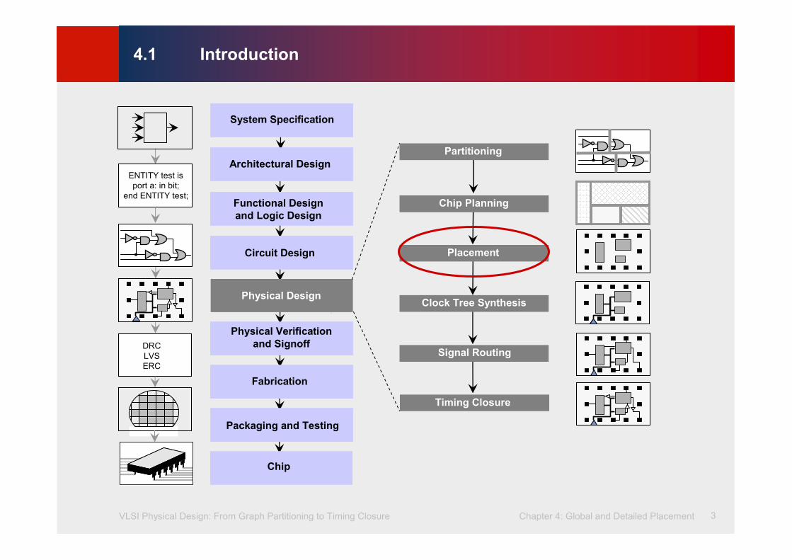
4.1 Introduction
ENTITY test isport a: in bit;
end ENTITY test;
DRC
LVSERC
Circuit Design
Functional Design
and Logic Design
Physical Design
Physical Verification
and Signoff
Fabrication
System Specification
Architectural Design
Chip
Packaging and Testing
Chip Planning
Placement
Signal Routing
Partitioning
Timing Closure
Clock Tree Synthesis
VLSI Physical Design: From Graph Partitioning to Timing Closure Chapter 4: Global and Detailed Placement 4
©KLMH
Lienig
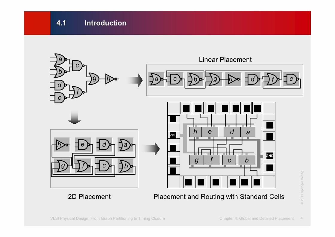
4.1 Introduction
©2011 Springer Verlag
c
h
f
b
a
gd
e
a c b hg d ef
eh
g f
d a
c b
GND
VDD
Linear Placement
2D Placement Placement and Routing with Standard Cells
h e d a
g f c b
VLSI Physical Design: From Graph Partitioning to Timing Closure Chapter 4: Global and Detailed Placement 5
©KLMH
Lienig
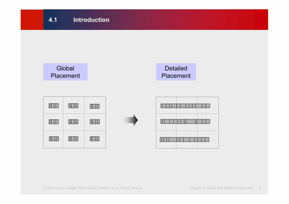
4.1 Introduction
Global
Placement
Detailed
Placement

VLSI Physical Design: From Graph Partitioning to Timing Closure Chapter 4: Global and Detailed Placement 6
©KLMH
Lienig
4.2 Optimization Objectives
Total
Wirelength
Number of
Cut Nets
Wire
CongestionSignal
Delay
©2011 Springer Verlag

VLSI Physical Design: From Graph Partitioning to Timing Closure Chapter 4: Global and Detailed Placement 7
©KLMH
Lienig
4.2 Optimization Objectives – Total Wirelength
a
b
c
e
dg
f
h
i
j
l
k
c ed
g
f h
il
k
j
a
b
©2011 Springer Verlag

VLSI Physical Design: From Graph Partitioning to Timing Closure Chapter 4: Global and Detailed Placement 8
©KLMH
Lienig
Wirelength estimation for a given placement
4.2 Optimization Objectives – Total Wirelength
Half-perimeter
wirelength
(HPWL)
HPWL = 9
4
5
Complete
graph
(clique)
8
6
5
33
4
Clique Length =
(2/p)Σe ∈ cliquedM(e) = 14.5
Monotone
chain
Chain Length = 12
63
3
Star model
Star Length = 15
83
4
Sait, S. M., Youssef, H.: VLSI Physical Design Automation, World Scientific
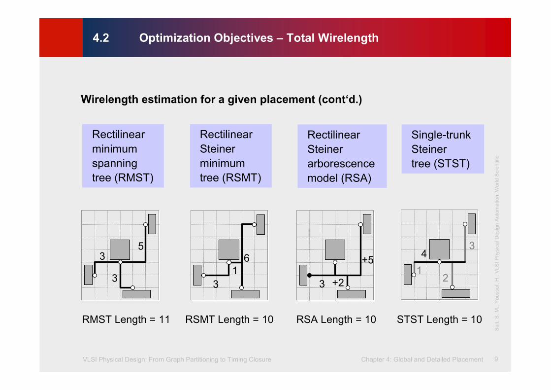
VLSI Physical Design: From Graph Partitioning to Timing Closure Chapter 4: Global and Detailed Placement 9
©KLMH
Lienig
Sait, S. M., Youssef, H.: VLSI Physical Design Automation, World Scientific
4.2 Optimization Objectives – Total Wirelength
Wirelength estimation for a given placement (cont‘d.)
Rectilinear
minimum
spanning
tree (RMST)
RMST Length = 11
3
3
5
Rectilinear
Steiner
minimum
tree (RSMT)
RSMT Length = 10
3
1
6
Rectilinear
Steiner
arborescence
model (RSA)
RSA Length = 10
+5
3 +2
Single-trunk
Steiner
tree (STST)
STST Length = 10
3
12
4
VLSI Physical Design: From Graph Partitioning to Timing Closure Chapter 4: Global and Detailed Placement 10
©KLMH
Lienig
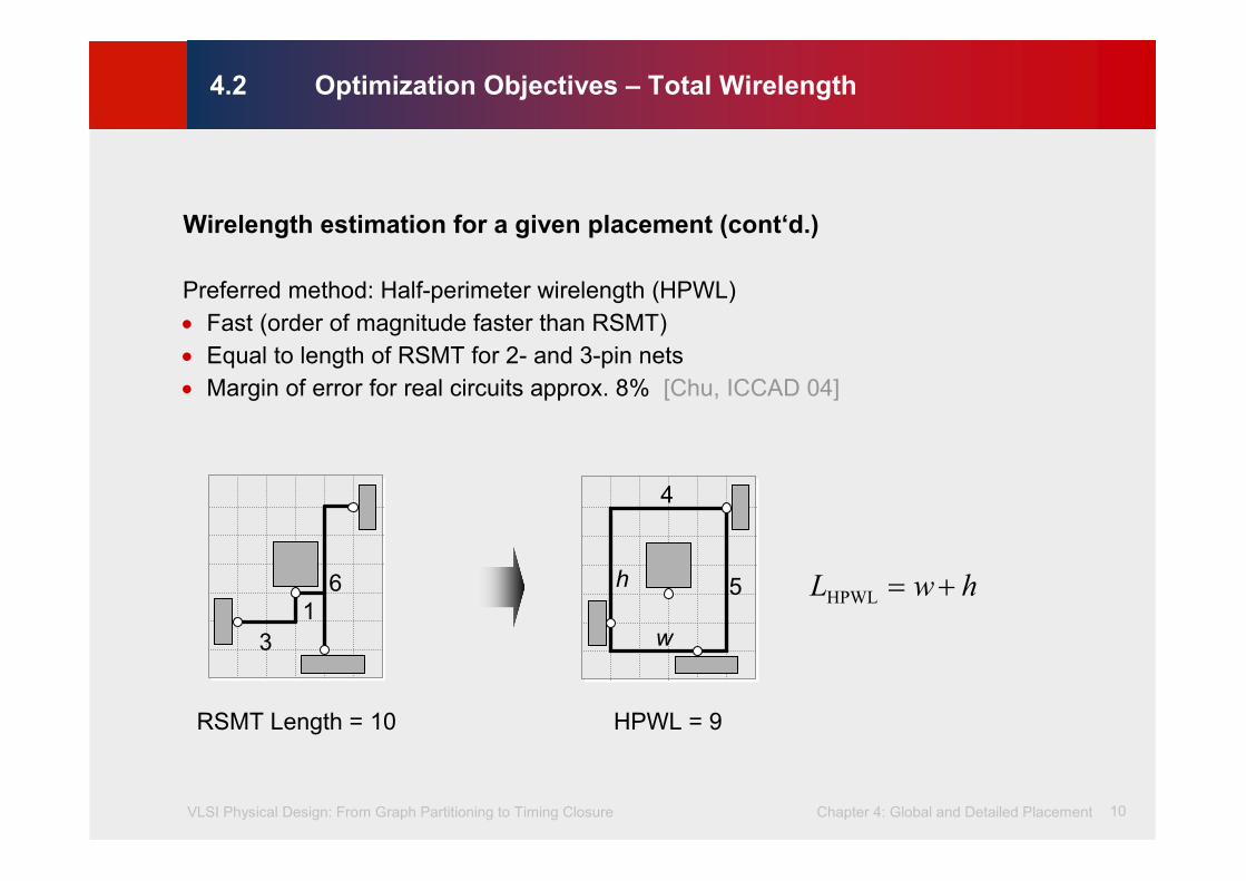
Preferred method: Half-perimeter wirelength (HPWL)
• Fast (order of magnitude faster than RSMT)
• Equal to length of RSMT for 2- and 3-pin nets
• Margin of error for real circuits approx. 8% [Chu, ICCAD 04]
hwL +=HPWL
4.2 Optimization Objectives – Total Wirelength
RSMT Length = 10
3
1
6
HPWL = 9
4
5
w
h
Wirelength estimation for a given placement (cont‘d.)

VLSI Physical Design: From Graph Partitioning to Timing Closure Chapter 4: Global and Detailed Placement 11
©KLMH
Lienig
4.2 Optimization Objectives – Total Wirelength
Total wirelength with net weights (weighted wirelength)
• For a placement P, an estimate of total weighted wirelength is
where w(net) is the weight of net, and L(net) is the estimated wirelength of net.
• Example:
∑∈
⋅=Pnet
netLnetwPL )()()(
33314472)()()( =⋅+⋅+⋅=⋅= ∑∈Pnet
netLnetwPL
a
b
d
c
f
e
b1 e1
c1
a1
d1
d2 f2
f1
Nets Weights
N1 = (a1, b1, d2) w(N1) = 2
N2 = (c1, d1, f1) w(N2) = 4
N3 = (e1, f2) w(N3) = 1

VLSI Physical Design: From Graph Partitioning to Timing Closure Chapter 4: Global and Detailed Placement 12
©KLMH
Lienig
4.2 Optimization Objectives – Number of Cut Nets
Cut sizes of a placement
• To improve total wirelength of a placement P, separately calculate the number
of crossings of global vertical and horizontal cutlines, and minimize
where ΨP(cut) be the set of nets cut by a cutline cut
∑∑∈∈
+=
PP Hh
P
Vv
P hvPL )(ψ)(ψ)(

VLSI Physical Design: From Graph Partitioning to Timing Closure Chapter 4: Global and Detailed Placement 13
©KLMH
Lienig
4.2 Optimization Objectives – Number of Cut Nets
Cut sizes of a placement
• Example:
• Cut values for each global cutline
ψP(v1) = 1 ψP(v2) = 2
ψP(h1) = 3 ψP(h2) = 2
• Total number of crossings in P
ψP(v1) + ψP(v2) + ψP(h1) + ψP(h2) = 1 + 2 + 3 + 2 = 8
• Cut sizes
X(P) = max(ψP(v1),ψP(v2)) = max(1,2) = 2
Y(P) = max(ψP(h1),ψP(h2)) = max(3,2) = 3
Nets
N1 = (a1, b1, d2)
N2 = (c1, d1, f1)
N3 = (e1, f2)
a
b
d
c
f
b1 e1
c1
d1
d2
a1
e
v1 v2
h2
h1 f2
f1
VLSI Physical Design: From Graph Partitioning to Timing Closure Chapter 4: Global and Detailed Placement 14
©KLMH
Lienig
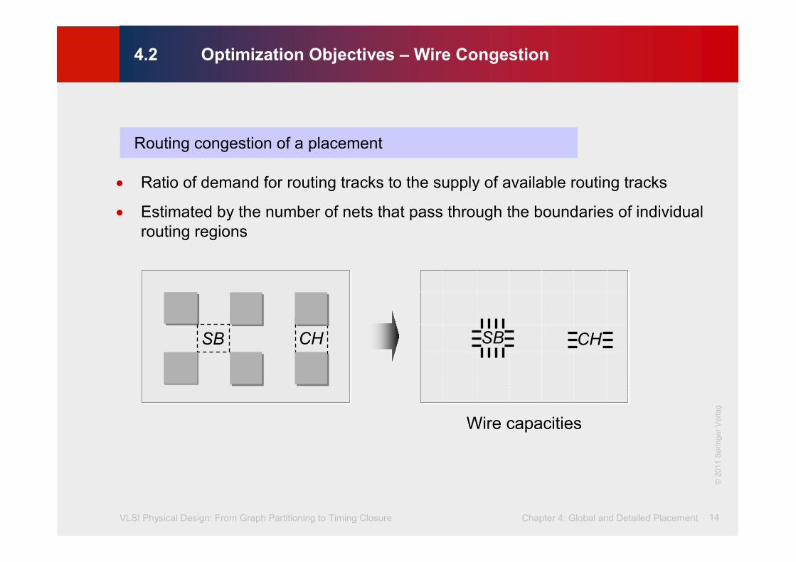
4.2 Optimization Objectives – Wire Congestion
Routing congestion of a placement
• Ratio of demand for routing tracks to the supply of available routing tracks
• Estimated by the number of nets that pass through the boundaries of individual
routing regions
SBCH CHSB
Wire capacities
©2011 Springer Verlag

VLSI Physical Design: From Graph Partitioning to Timing Closure Chapter 4: Global and Detailed Placement 15
©KLMH
Lienig
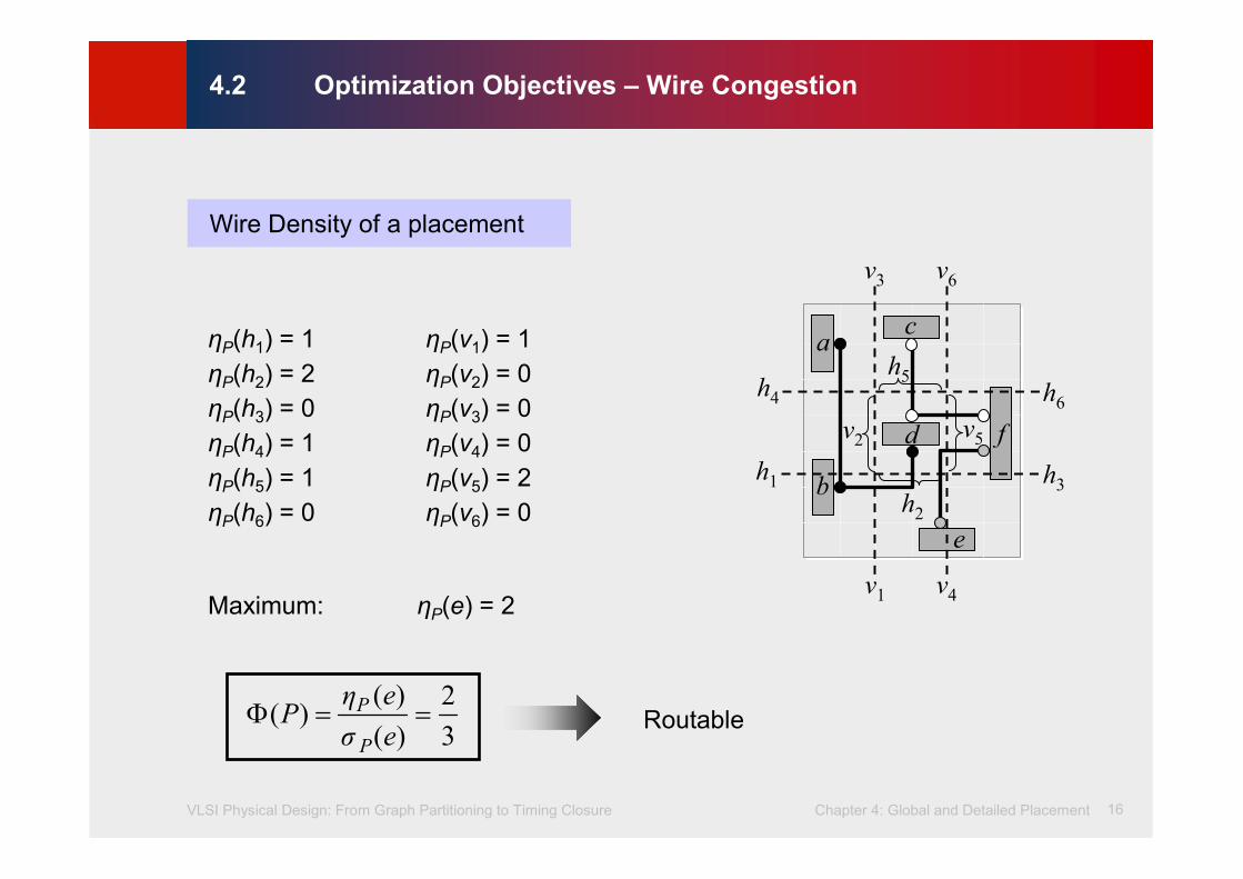
4.2 Optimization Objectives – Wire Congestion
Routing congestion of a placement
• Formally, the local wire density φP(e) of an edge e between two neighboring
grid cells is
where ηP(e) is the estimated number of nets that cross e and
σP(e) is the maximum number of nets that can cross e
• If φP(e) > 1, then too many nets are estimated to cross e, making P more likely
to be unroutable.
• The wire density of P is
where E is the set of all edges
• If Φ(P) ≤ 1, then the design is estimated to be fully routable, otherwise routing
will need to detour some nets through less-congested edges
)(σ
)(η)(φ
e
ee
P
PP =
( ))(φmax)( eP PEe∈
=Φ
VLSI Physical Design: From Graph Partitioning to Timing Closure Chapter 4: Global and Detailed Placement 16
©KLMH
Lienig
4.2 Optimization Objectives – Wire Congestion
Wire Density of a placement
a
b
c
f
e
h5
h2
v2
v1 v4
h4
h1
h6
h3
v3 v6
d v5
ηP(h1) = 1
ηP(h2) = 2
ηP(h3) = 0
ηP(h4) = 1
ηP(h5) = 1
ηP(h6) = 0
ηP(v1) = 1
ηP(v2) = 0
ηP(v3) = 0
ηP(v4) = 0
ηP(v5) = 2
ηP(v6) = 0
Maximum: ηP(e) = 2
3
2
)(
)()( ==Φ
eσ
eηP
P
PRoutable
VLSI Physical Design: From Graph Partitioning to Timing Closure Chapter 4: Global and Detailed Placement 17
©KLMH
Lienig
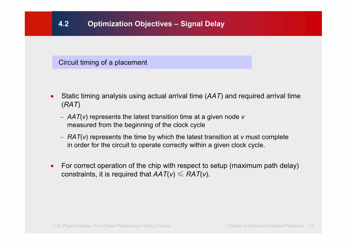
4.2 Optimization Objectives – Signal Delay
Circuit timing of a placement
• Static timing analysis using actual arrival time (AAT) and required arrival time
(RAT)
− AAT(v) represents the latest transition time at a given node v
measured from the beginning of the clock cycle
− RAT(v) represents the time by which the latest transition at v must complete
in order for the circuit to operate correctly within a given clock cycle.
• For correct operation of the chip with respect to setup (maximum path delay)
constraints, it is required that AAT(v) ≤ RAT(v).

VLSI Physical Design: From Graph Partitioning to Timing Closure Chapter 4: Global and Detailed Placement 18
©KLMH
Lienig
Global Placement
4.1 Introduction
4.2 Optimization Objectives
4.3 Global Placement
4.3.1 Min-Cut Placement
4.3.2 Analytic Placement
4.3.3 Simulated Annealing
4.3.4 Modern Placement Algorithms
4.4 Legalization and Detailed Placement

VLSI Physical Design: From Graph Partitioning to Timing Closure Chapter 4: Global and Detailed Placement 19
©KLMH
Lienig
• Partitioning-based algorithms:
− The netlist and the layout are divided into smaller sub-netlists and sub-regions,
respectively
− Process is repeated until each sub-netlist and sub-region is small enough
to be handled optimally
− Detailed placement often performed by optimal solvers, facilitating a natural
transition from global placement to detailed placement
− Example: min-cut placement
• Analytic techniques:
− Model the placement problem using an objective (cost) function,
which can be optimized via numerical analysis
− Examples: quadratic placement and force-directed placement
• Stochastic algorithms:
− Randomized moves that allow hill-climbing are used to optimize the cost
function
− Example: simulated annealing
Global Placement

VLSI Physical Design: From Graph Partitioning to Timing Closure Chapter 4: Global and Detailed Placement 20
©KLMH
Lienig
StochasticPartitioning-based Analytic
Quadratic
placement
Min-cut
placement
Simulated annealingForce-directed
placement
Global Placement

VLSI Physical Design: From Graph Partitioning to Timing Closure Chapter 4: Global and Detailed Placement 21
©KLMH
Lienig
4.3.1 Min-Cut Placement
• Uses partitioning algorithms to divide (1) the netlist and (2) the layout region
into smaller sub-netlists and sub-regions
• Conceptually, each sub-region is assigned a portion of the original netlist
• Each cut heuristically minimizes the number of cut nets using, for example,
− Kernighan-Lin (KL) algorithm
− Fiduccia-Mattheyses (FM) algorithm
VLSI Physical Design: From Graph Partitioning to Timing Closure Chapter 4: Global and Detailed Placement 22
©KLMH
Lienig
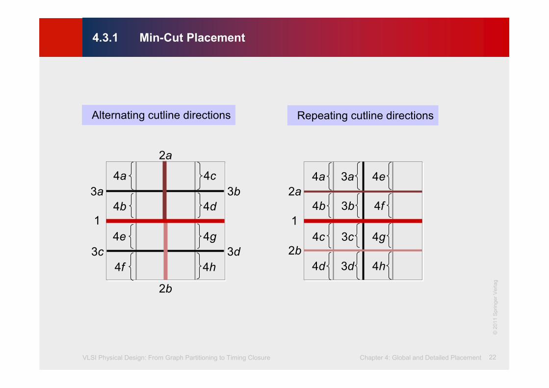
Alternating cutline directions
4.3.1 Min-Cut Placement
1
2b
3a
3c
2a
3b
3d
4b
4c4a
4d
4f
4g4e
4h
1
2a
2b
3a
3b
3c
3d
4a
4b
4c
4d
4e
4f
4g
4h
Repeating cutline directions
©2011 Springer Verlag

VLSI Physical Design: From Graph Partitioning to Timing Closure Chapter 4: Global and Detailed Placement 23
©KLMH
Lienig
Input: netlist Netlist, layout area LA, minimum number of cells per region cells_min
Output: placement P
P = Ø
regions = ASSIGN(Netlist,LA) // assign netlist to layout area
while (regions != Ø) // while regions still not placed
region = FIRST_ELEMENT(regions) // first element in regions
REMOVE(regions, region) // remove first element of regions
if (region contains more than cell_min cells)
(sr1,sr2) = BISECT(region) // divide region into two subregions
// sr1 and sr2, obtaining the sub-
// netlists and sub-areas
ADD_TO_END(regions,sr1) // add sr1 to the end of regions
ADD_TO_END(regions,sr2) // add sr2 to the end of regions
else
PLACE(region) // place region
ADD(P,region) // add region to P
4.3.1 Min-Cut Placement

VLSI Physical Design: From Graph Partitioning to Timing Closure Chapter 4: Global and Detailed Placement 24
©KLMH
Lienig
Given:
Task: 4 x 2 placement with minimum wirelength using alternative
cutline directions and the KL algorithm
1
2
3
4
5 6
4.3.1 Min-Cut Placement – Example
cut1

VLSI Physical Design: From Graph Partitioning to Timing Closure Chapter 4: Global and Detailed Placement 25
©KLMH
Lienig
4.3.1 Min-Cut-Platzierung: Beispiel
Vertical cut cut1: L={1,2,3}, R={4,5,6}
1
2
3
0
4
5
6
0
1
2 3
0
4 5
6
0
cut1 cut1
1
2
3
4
5 6
cut1
KL Algorithmus

VLSI Physical Design: From Graph Partitioning to Timing Closure Chapter 4: Global and Detailed Placement 26
©KLMH
Lienig
Horizontal cut cut2L: T={1,4}, B={2,0}
1
2 0
4
Horizontal cut cut2R: T={3,5}, B={6,0}
3 5
60
cut2L cut2R
1 4 5 3
2 6
1
2 3
0
4 5
6
0
cut1
1
20
4 5 3
06
cut3BL cut3BR
cut3TL cut3TR

VLSI Physical Design: From Graph Partitioning to Timing Closure Chapter 4: Global and Detailed Placement 27
©KLMH
Lienig
2
1
3
4 1
2
4
3
2
1
4
3
p‘
BR
TR
BR
TR
2
1
43
x
2
1
43
1
2 4
3
4.3.1 Min-Cut Placement – Terminal Propagation
• Terminal Propagation
− External connections are represented by artificial connection points
on the cutline
− Dummy nodes in hypergraphs
©2011 Springer Verlag
VLSI Physical Design: From Graph Partitioning to Timing Closure Chapter 4: Global and Detailed Placement 28
©KLMH
Lienig
4.3.1 Min-Cut Placement
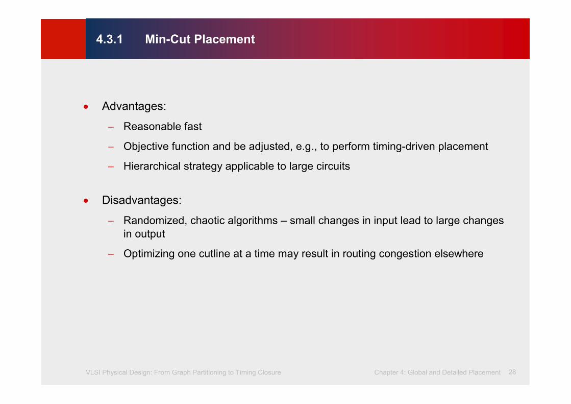
• Advantages:
− Reasonable fast
− Objective function and be adjusted, e.g., to perform timing-driven placement
− Hierarchical strategy applicable to large circuits
• Disadvantages:
− Randomized, chaotic algorithms – small changes in input lead to large changes
in output
− Optimizing one cutline at a time may result in routing congestion elsewhere
VLSI Physical Design: From Graph Partitioning to Timing Closure Chapter 4: Global and Detailed Placement 29
©KLMH
Lienig
4.3.2 Analytic Placement – Quadratic Placement
• Objective function is quadratic; sum of (weighted) squared Euclidean distance
represents placement objective function
where n is the total number of cells, and c(i,j) is the connection cost between cells i and j.
• Only two-point-connections
• Minimize objective function by equating its derivative to zero
which reduces to solving a system of linear equations
( ) ( )( )∑=
−+−=n
ji
jijiij yyxxcPL1,
22
2
1)(
VLSI Physical Design: From Graph Partitioning to Timing Closure Chapter 4: Global and Detailed Placement 30
©KLMH
Lienig30
4.3.2 Analytic Placement – Quadratic Placement
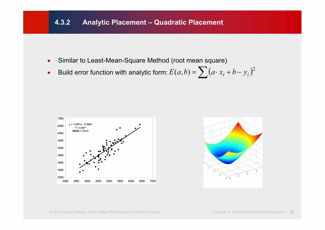
• Similar to Least-Mean-Square Method (root mean square)
• Build error function with analytic form: ( )∑ −+⋅=2
),( ii ybxabaE

VLSI Physical Design: From Graph Partitioning to Timing Closure Chapter 4: Global and Detailed Placement 31
©KLMH
Lienig
4.3.2 Analytic Placement – Quadratic Placement
where n is the total number of cells, and c(i,j) is the connection cost between cells i and j.
• Each dimension can be considered independently:
• Convex quadratic optimization problem: any local minimum solution
is also a global minimum
• Optimal x- and y--coordinates can be found by setting the partial derivatives
of Lx(P) and Ly(P) to zero
( ) ( )( )∑=
−+−=n
ji
jijiij yyxxcPL1,
22
2
1)(
2
1,1
)(),()( ji
n
ji
x xxjicPL −= ∑==
2
1,1
)(),()( ji
n
ji
y yyjicPL −= ∑==

VLSI Physical Design: From Graph Partitioning to Timing Closure Chapter 4: Global and Detailed Placement 32
©KLMH
Lienig
4.3.2 Analytic Placement – Quadratic Placement
where n is the total number of cells, and c(i,j) is the connection cost between cells i and j.
• Each dimension can be considered independently:
• where A is a matrix with A[i][j] = -c(i,j) when i≠ j,
and A[i][i] = the sum of incident connection weights of cell i.
• X is a vector of all the x-coordinates of the non-fixed cells, and bx is a vector
with bx[i] = the sum of x-coordinates of all fixed cells attached to i.
• Y is a vector of all the y-coordinates of the non-fixed cells, and by is a vector
with by[i] = the sum of y-coordinates of all fixed cells attached to i.
( ) ( )( )∑=
−+−=n
ji
jijiij yyxxcPL1,
22
2
1)(
2
1,1
)(),()( ji
n
ji
x xxjicPL −= ∑==
2
1,1
)(),()( ji
n
ji
y yyjicPL −= ∑==
0)(
=−=∂
∂x
x bAXX
PL0
)(=−=
∂
∂y
ybAY
Y
PL

VLSI Physical Design: From Graph Partitioning to Timing Closure Chapter 4: Global and Detailed Placement 33
©KLMH
Lienig
4.3.2 Analytic Placement – Quadratic Placement
where n is the total number of cells, and c(i,j) is the connection cost between cells i and j.
• Each dimension can be considered independently:
• System of linear equations for which iterative numerical methods can be used
to find a solution
( ) ( )( )∑=
−+−=n
ji
jijiij yyxxcPL1,
22
2
1)(
2
1,1
)(),()( ji
n
ji
x xxjicPL −= ∑==
2
1,1
)(),()( ji
n
ji
y yyjicPL −= ∑==
0)(
=−=∂
∂x
x bAXX
PL0
)(=−=
∂
∂y
ybAY
Y
PL

VLSI Physical Design: From Graph Partitioning to Timing Closure Chapter 4: Global and Detailed Placement 34
©KLMH
Lienig
• Mechanical analogy: mass-spring system
− Squared Euclidean distance is proportional to the energy of a spring
between these points
− Quadratic objective function represents total energy of the spring system;
for each movable object, the x (y) partial derivative represents the total force
acting on that object
− Setting the forces of the nets to zero, an equilibrium state is mathematically
modeled that is characterized by zero forces acting on each movable object
− At the end, all springs are in a force equilibrium with a minimal total spring
energy; this equilibrium represents the minimal sum of squared wirelength
→ Result: many cell overlaps
4.3.2 Analytic Placement – Quadratic Placement

VLSI Physical Design: From Graph Partitioning to Timing Closure Chapter 4: Global and Detailed Placement 35
©KLMH
Lienig
• Second stage of quadratic placers: cells are spread out to remove overlaps
• Methods:
− Adding fake nets that pull cells away from dense regions toward anchors
− Geometric sorting and scaling
− Repulsion forces, etc.
4.3.2 Analytic Placement – Quadratic Placement
VLSI Physical Design: From Graph Partitioning to Timing Closure Chapter 4: Global and Detailed Placement 36
©KLMH
Lienig
• Advantages:
− Captures the placement problem concisely in mathematical terms
− Leverages efficient algorithms from numerical analysis and available software
− Can be applied to large circuits without netlist clustering (flat)
− Stability: small changes in the input do not lead to large changes in the output
• Disadvantages:
− Connections to fixed objects are necessary: I/O pads, pins of fixed macros, etc.
4.3.2 Analytic Placement – Quadratic Placement

VLSI Physical Design: From Graph Partitioning to Timing Closure Chapter 4: Global and Detailed Placement 37
©KLMH
Lienig
• Cells and wires are modeled using the mechanical analogy of a mass-spring
system, i.e., masses connected to Hooke’s-Law springs
• Attraction force between cells is directly proportional to their distance
• Cells will eventually settle in a force equilibrium→ minimized wirelength
4.3.2 Analytic Placement – Force-directed Placement

VLSI Physical Design: From Graph Partitioning to Timing Closure Chapter 4: Global and Detailed Placement 38
©KLMH
Lienig
• Given two connected cells a and b, the attraction force exerted on a by b is
where
− c(a,b) is the connection weight (priority) between cells a and b, and
− is the vector difference of the positions of a and b in the Euclidean plane
• The sum of forces exerted on a cell i connected to other cells 1… j is
• Zero-force target (ZFT): position that minimizes this sum of forces
4.3.2 Analytic Placement – Force-directed Placement
abF
)(),( abbacFab −⋅=
∑≠
=
0),( jic
iji FF
)( ab −

VLSI Physical Design: From Graph Partitioning to Timing Closure Chapter 4: Global and Detailed Placement 39
©KLMH
Lienig
Zero-Force-Target (ZFT) position of cell i
4.3.2 Analytic Placement – Force-directed Placement
min Fi = c(i,a) · (a – i ) + c(i,b) · (b – i ) + c(i,c) · (c – i ) + c(i,d) · (d – i )
a
b
c
d
i
ZFT Position
©2011 Springer Verlag

VLSI Physical Design: From Graph Partitioning to Timing Closure Chapter 4: Global and Detailed Placement 40
©KLMH
Lienig
Basic force-directed placement
4.3.2 Analytic Placement – Force-directed Placement
• Iteratively moves all cells to their respective ZFT positions
• x- and y-direction forces are set to zero:
• Rearranging the variables to solve for xi0 and yi
0 yields
0)(),(
0),(
00 =−⋅∑≠jic
ij xxjic 0)(),(
0),(
00 =−⋅∑≠jic
ij yyjic
∑
∑
≠
≠
⋅
=
0),(
0),(
0
0
),(
),(
jic
jic
j
ijic
xjic
x
∑
∑
≠
≠
⋅
=
0),(
0),(
0
0
),(
),(
jic
jic
j
ijic
yjic
y
Computation of
ZFT position of cell i
connected with
cells 1 … j

VLSI Physical Design: From Graph Partitioning to Timing Closure Chapter 4: Global and Detailed Placement 41
©KLMH
Lienig
0 1 2
1
2
In2
In3
In1
Out
In1
In2
In3
Out1
Example: ZFT position
4.3.2 Analytic Placement – Force-directed Placement
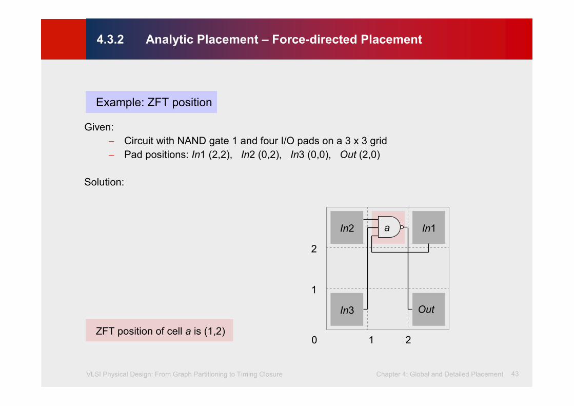
Given:
− Circuit with NAND gate 1 and four I/O pads on a 3 x 3 grid
− Pad positions: In1 (2,2), In2 (0,2), In3 (0,0), Out (2,0)
− Weighted connections: c(a,In1) = 8, c(a,In2) = 10, c(a,In3) = 2, c(a,Out) = 2
Task: find the ZFT position of cell a

VLSI Physical Design: From Graph Partitioning to Timing Closure Chapter 4: Global and Detailed Placement 42
©KLMH
Lienig
4.3.2 Analytic Placement – Force-directed Placement
Given:
− Circuit with NAND gate 1 and four I/O pads on a 3 x 3 grid
− Pad positions: In1 (2,2), In2 (0,2), In3 (0,0), Out (2,0)
Solution:
ZFT position of cell a is (1,2)
),()3,()2,()1,(
),()3,()2,()1,(
),(
),(
321
0),(
0),(
0
0
OutacInacInacInac
xOutacxInacxInacxInac
jac
xjac
x OutInInIn
jic
jic
j
a+++
⋅+⋅+⋅+⋅=
⋅
=
∑
∑
≠
≠9.0
22
20
22108
220201028≈=
+++
⋅+⋅+⋅+⋅=
),()3,()2,()1,(
),()3,()2,()1,(
),(
),(
321
0),(
0),(
0
0
OutacInacInacInac
yOutacyInacyInacyInac
jac
yjac
y OutInInIn
jic
jic
j
a+++
⋅+⋅+⋅+⋅=
⋅
=∑
∑
≠
≠ 6.122
36
22108
020221028≈=
+++
⋅+⋅+⋅+⋅=
Example: ZFT position
VLSI Physical Design: From Graph Partitioning to Timing Closure Chapter 4: Global and Detailed Placement 43
©KLMH
Lienig
4.3.2 Analytic Placement – Force-directed Placement
0 1 2
1
2
In2
In3
In1
Out
a
Given:
− Circuit with NAND gate 1 and four I/O pads on a 3 x 3 grid
− Pad positions: In1 (2,2), In2 (0,2), In3 (0,0), Out (2,0)
Solution:
Example: ZFT position
ZFT position of cell a is (1,2)
VLSI Physical Design: From Graph Partitioning to Timing Closure Chapter 4: Global and Detailed Placement 44
©KLMH
Lienig
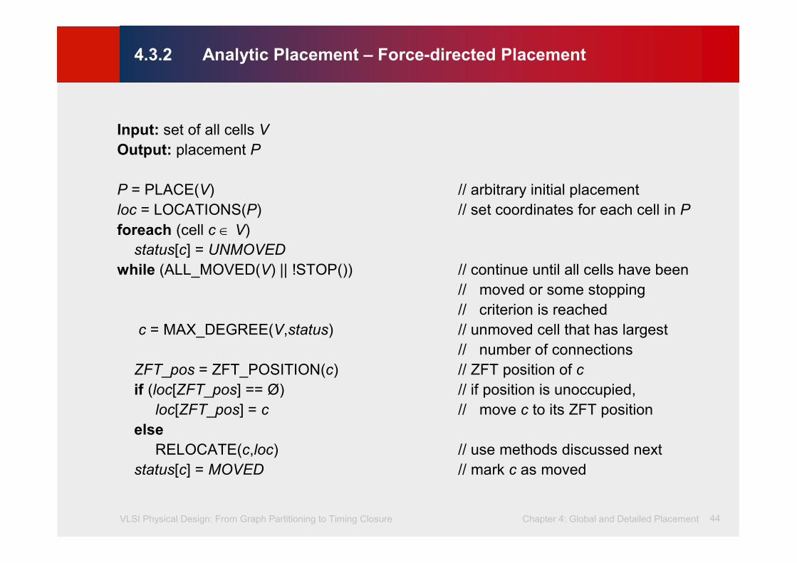
4.3.2 Analytic Placement – Force-directed Placement
Input: set of all cells V
Output: placement P
P = PLACE(V) // arbitrary initial placement
loc = LOCATIONS(P) // set coordinates for each cell in P
foreach (cell c ∈ V)
status[c] = UNMOVED
while (ALL_MOVED(V) || !STOP()) // continue until all cells have been
// moved or some stopping
// criterion is reached
c = MAX_DEGREE(V,status) // unmoved cell that has largest
// number of connections
ZFT_pos = ZFT_POSITION(c) // ZFT position of c
if (loc[ZFT_pos] == Ø) // if position is unoccupied,
loc[ZFT_pos] = c // move c to its ZFT position
else
RELOCATE(c,loc) // use methods discussed next
status[c] = MOVED // mark c as moved

VLSI Physical Design: From Graph Partitioning to Timing Closure Chapter 4: Global and Detailed Placement 45
©KLMH
Lienig
Finding a valid location for a cell with an occupied ZFT position
(p: incoming cell, q: cell in p‘s ZFT position)
• If possible, move p to a cell position close to q.
• Chain move: cell p is moved to cells q’s location.
− Cell q, in turn, is shifted to the next position. If a cell r is occupying this space,
cell r is shifted to the next position.
− This continues until all affected cells are placed.
• Compute the cost difference if p and q were to be swapped.
If the total cost reduces, i.e., the weighted connection length L(P) is smaller,
then swap p and q.
4.3.2 Analytic Placement – Force-directed Placement

VLSI Physical Design: From Graph Partitioning to Timing Closure Chapter 4: Global and Detailed Placement 46
©KLMH
Lienig
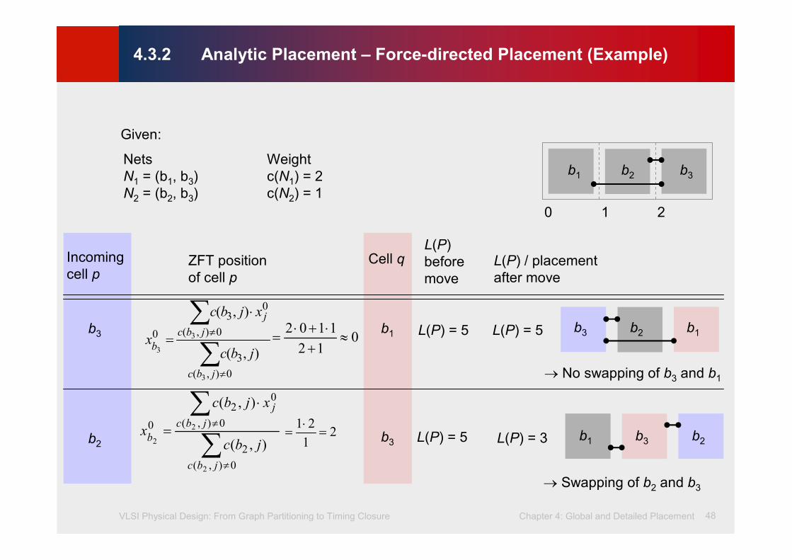
Nets Weight
N1 = (b1, b3) c(N1) = 2
N2 = (b2, b3) c(N2) = 1
Given:
4.3.2 Analytic Placement – Force-directed Placement (Example)
b1 b3b2
0 1 2

VLSI Physical Design: From Graph Partitioning to Timing Closure Chapter 4: Global and Detailed Placement 47
©KLMH
Lienig
Incoming
cell pZFT position
of cell p
L(P)
before
move
L(P) / placement
after move
b3 L(P) = 5
Cell q
b1
Nets Weight
N1 = (b1, b3) c(N1) = 2
N2 = (b2, b3) c(N2) = 1
Given:
∑
∑
≠
≠
⋅
=
0),(
3
0),(
03
0
3
3
3 ),(
),(
jbc
jbc
j
bjbc
xjbc
x 012
1102≈
+
⋅+⋅=
4.3.2 Analytic Placement – Force-directed Placement (Example)
3 12L(P) = 5
⇒ No swapping of b3 and b1
b3 b1b2
b1 b3b2
0 1 2
VLSI Physical Design: From Graph Partitioning to Timing Closure Chapter 4: Global and Detailed Placement 48
©KLMH
Lienig
Incoming
cell pZFT position
of cell p
L(P)
before
move
L(P) / placement
after move
b3 L(P) = 5
Cell q
b1 3 12
Nets Weight
N1 = (b1, b3) c(N1) = 2
N2 = (b2, b3) c(N2) = 1
Given:
b1 b3b2
0 1 2
∑
∑
≠
≠
⋅
=
0),(
3
0),(
03
0
3
3
3 ),(
),(
jbc
jbc
j
bjbc
xjbc
x 012
1102≈
+
⋅+⋅= L(P) = 5
→ No swapping of b3 and b1
b3 b1b2
4.3.2 Analytic Placement – Force-directed Placement (Example)
b2 L(P) = 3L(P) = 5b3b1 b2b3∑
∑
≠
≠
⋅
=
0),(
2
0),(
02
0
2
2
2 ),(
),(
jbc
jbc
j
bjbc
xjbc
x 21
21=
⋅=
→ Swapping of b2 and b3

VLSI Physical Design: From Graph Partitioning to Timing Closure Chapter 4: Global and Detailed Placement 49
©KLMH
Lienig
• Advantages:
− Conceptually simple, easy to implement
− Primarily intended for global placement, but can also be adapted to detailed
placement
• Disadvantages:
− Does not scale to large placement instances
− Is not very effective in spreading cells in densest regions
− Poor trade-off between solution quality and runtime
• In practice, FDP is extended by specialized techniques for cell spreading
− This facilitates scalability and makes FDP competitive
4.3.2 Analytic Placement – Force-directed Placement
VLSI Physical Design: From Graph Partitioning to Timing Closure Chapter 4: Global and Detailed Placement 50
©KLMH
Lienig
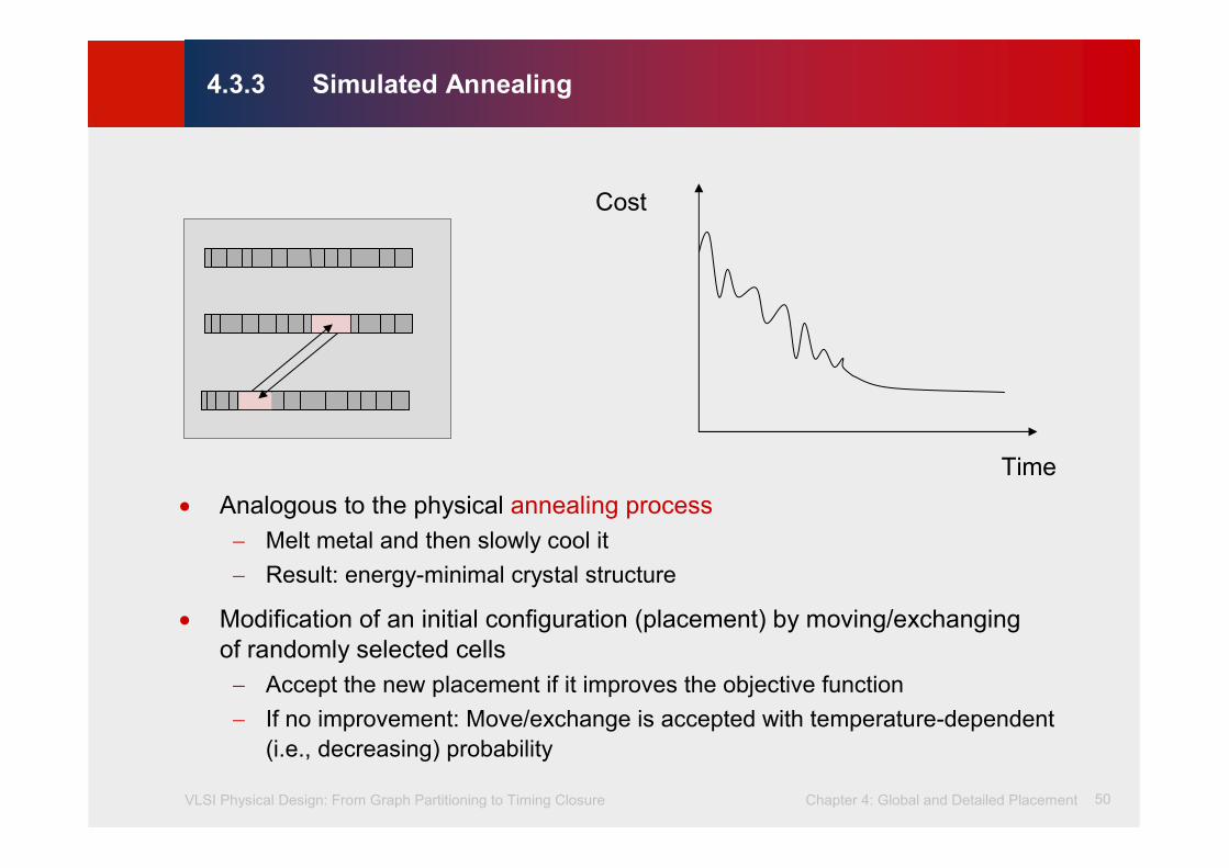
4.3.3 Simulated Annealing
Time
Cost
• Analogous to the physical annealing process
− Melt metal and then slowly cool it
− Result: energy-minimal crystal structure
• Modification of an initial configuration (placement) by moving/exchanging
of randomly selected cells
− Accept the new placement if it improves the objective function
− If no improvement: Move/exchange is accepted with temperature-dependent
(i.e., decreasing) probability

VLSI Physical Design: From Graph Partitioning to Timing Closure Chapter 4: Global and Detailed Placement 51
©KLMH
Lienig
Input: set of all cells V
Output: placement P
T = T0 // set initial temperature
P = PLACE(V) // arbitrary initial placement
while (T > Tmin)
while (!STOP()) // not yet in equilibrium at T
new_P = PERTURB(P)
Δcost = COST(new_P) – COST(P)
if (Δcost < 0) // cost improvement
P = new_P // accept new placement
else // no cost improvement
r = RANDOM(0,1) // random number [0,1)
if (r < e -Δcost/T) // probabilistically accept
P = new_P
T = α · T // reduce T, 0 < α < 1
4.3.3 Simulated Annealing – Algorithm

VLSI Physical Design: From Graph Partitioning to Timing Closure Chapter 4: Global and Detailed Placement 52
©KLMH
Lienig
• Advantages:
− Can find global optimum (given sufficient time)
− Well-suited for detailed placement
• Disadvantages:
− Very slow
− To achieve high-quality implementation, laborious parameter tuning is necessary
− Randomized, chaotic algorithms - small changes in the input
lead to large changes in the output
• Practical applications of SA:
− Very small placement instances with complicated constraints
− Detailed placement, where SA can be applied in small windows
(not common anymore)
− FPGA layout, where complicated constraints are becoming a norm
4.3.3 Simulated Annealing

VLSI Physical Design: From Graph Partitioning to Timing Closure Chapter 4: Global and Detailed Placement 53
©KLMH
Lienig53
4.3.3 Simulated Annealing
Time
Cost
• Analogous to the physical annealing process
− Melt metal and then slowly cool it
− Result: energy-minimal crystal structure
• Modification of an initial configuration (placement) by moving/exchanging
of randomly selected cells
− Accept the new placement if it improves the objective function
− If no improvement: Move/exchange is accepted with temperature-dependent
(i.e., decreasing) probability
VLSI Physical Design: From Graph Partitioning to Timing Closure Chapter 4: Global and Detailed Placement 54
©KLMH
Lienig
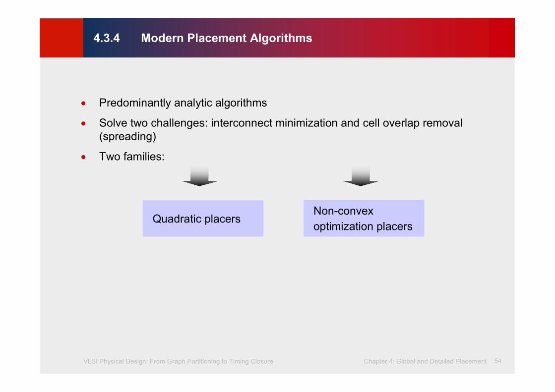
• Predominantly analytic algorithms
• Solve two challenges: interconnect minimization and cell overlap removal
(spreading)
• Two families:
4.3.4 Modern Placement Algorithms
Quadratic placersNon-convex
optimization placers

VLSI Physical Design: From Graph Partitioning to Timing Closure Chapter 4: Global and Detailed Placement 55
©KLMH
Lienig
• Solve large, sparse systems of linear equations (formulated
using force-directed placement) by the Conjugate Gradient algorithm
• Perform cell spreading by adding fake nets that pull cells away
from dense regions toward carefully placed anchors
4.3.4 Modern Placement Algorithms
Quadratic placersNon-convex
optimization placers

VLSI Physical Design: From Graph Partitioning to Timing Closure Chapter 4: Global and Detailed Placement 56
©KLMH
Lienig
• Model interconnect by sophisticated differentiable functions,
e.g., log-sum-exp is the popular choice
• Model cell overlap and fixed obstacles by additional (non-convex) functional
terms
• Optimize interconnect by the non-linear Conjugate Gradient algorithm
• Sophisticated, slow algorithms
• All leading placers in this category use netlist clustering to improve
computational scalability (this further complicates the implementation)
4.3.4 Modern Placement Algorithms
Quadratic placersNon-convex
optimization placers

VLSI Physical Design: From Graph Partitioning to Timing Closure Chapter 4: Global and Detailed Placement 57
©KLMH
Lienig
Pros and cons:
• Quadratic placers are simpler and faster, easier to parallelize
• Non-convex optimizers tend to produce better solutions
• As of 2011, quadratic placers are catching up in solution quality
while running 5-6 times faster [1]
4.3.4 Modern Placement Algorithms
Quadratic
Placement
Non-convex
optimization placers
[1] M.-C.Kim, D. Lee, I. L. Markov: SimPL: An effective placement algorithm.
ICCAD 2010: 649-656

VLSI Physical Design: From Graph Partitioning to Timing Closure Chapter 4: Global and Detailed Placement 58
©KLMH
Lienig
4.1 Introduction
4.2 Optimization Objectives
4.3 Global Placement
4.3.1 Min-Cut Placement
4.3.2 Analytic Placement
4.3.3 Simulated Annealing
4.3.4 Modern Placement Algorithms
4.4 Legalization and Detailed Placement
4.4 Legalization and Detailed Placement
VLSI Physical Design: From Graph Partitioning to Timing Closure Chapter 4: Global and Detailed Placement 59
©KLMH
Lienig
• Global placement must be legalized
− Cell locations typically do not align with power rails
− Small cell overlaps due to incremental changes, such as cell resizing or buffer
insertion
• Legalization seeks to find legal, non-overlapping placements for all placeable
modules
• Legalization can be improved by detailed placement techniques, such as
− Swapping neighboring cells to reduce wirelength
− Sliding cells to unused space
• Software implementations of legalization and detailed placement are often
bundled
4.4 Legalization and Detailed Placement

VLSI Physical Design: From Graph Partitioning to Timing Closure Chapter 4: Global and Detailed Placement 60
©KLMH
Lienig
4.4 Legalization and Detailed Placement
Power
Rail Standard Cell Row
VDD
GND
Legal positions of standard cells between VDD and GND rails
INV NAND NOR
©2011 Springer Verlag
VLSI Physical Design: From Graph Partitioning to Timing Closure Chapter 4: Global and Detailed Placement 61
©KLMH
Lienig
Summary of Chapter 4 – Problem Formulation and Objectives
• Row-based standard-cell placement
− Cell heights are typically fixed, to fit in rows (but some cells may have double
and quadruple heights)
− Legal cell sites facilitate the alignment of routing tracks, connection to power
and ground rails
• Wirelength as a key metric of interconnect
− Bounding box half-perimeter (HPWL)
− Cliques and stars
− RMSTs and RSMTs
• Objectives: wirelength, routing congestion, circuit delay
− Algorithm development is usually driven by wirelength
− The basic framework is implemented, evaluated and made competitive
on standard benchmarks
− Additional objectives are added to an operational framework

VLSI Physical Design: From Graph Partitioning to Timing Closure Chapter 4: Global and Detailed Placement 62
©KLMH
Lienig
Summary of Chapter 4 – Global Placement
• Combinatorial optimization techniques: min-cut and simulated annealing
− Can perform both global and detailed placement
− Reasonably good at small to medium scales
− SA is very slow, but can handle a greater variety of constraints
− Randomized and chaotic algorithms – small changes at the input can lead
to large changes at the output
• Analytic techniques: force-directed placement and non-convex optimization
− Primarily used for global placement
− Unrivaled for large netlists in speed and solution quality
− Capture the placement problem by mathematical optimization
− Use efficient numerical analysis algorithms
− Ensure stability: small changes at the input can cause only small changes
at the output
− Example: a modern, competitive analytic global placer takes 20mins for global
placement of a netlist with 2.1M cells (single thread, 3.2GHz Intel CPU) [1]
[1] M.-C.Kim, D. Lee, I. L. Markov: SimPL: An effective placement algorithm.
ICCAD 2010: 649-656

VLSI Physical Design: From Graph Partitioning to Timing Closure Chapter 4: Global and Detailed Placement 63
©KLMH
Lienig
Summary of Chapter 4 – Legalization and Detailed Placement
• Legalization ensures that design rules & constraints are satisfied
− All cells are in rows
− Cells align with routing tracks
− Cells connect to power & ground rails
− Additional constraints are often considered, e.g., maximum cell density
• Detailed placement reduces interconnect, while preserving legality
− Swapping neighboring cells, rotating groups of three
− Optimal branch-and-bound on small groups of cells
− Sliding cells along their rows
− Other local changes
• Extensions to optimize routed wirelength, routing congestion and circuit timing
• Relatively straightforward algorithms, but high-quality, fast implementation
is important
• Most relevant after analytic global placement, but are also used after min-cut
placement
• Rule of thumb: 50% runtime is spent in global placement, 50% in detailed
placement [1]
[1] M.-C.Kim, D. Lee, I. L. Markov: SimPL: An effective placement algorithm.
ICCAD 2010: 649-656


![Vorles-SeqTec 111206.ppt [Kompatibilitätsmodus] · DNA sequencing platforms 2x300 Gb/10d, ... stranded DNA templates ... Microsoft PowerPoint - Vorles-SeqTec_111206.ppt [Kompatibilitätsmodus]](https://img.dokumen.tips/doc/110x75/5aef00757f8b9ac2468c1b76/vorles-seqtec-kompatibilittsmodus-sequencing-platforms-2x300-gb10d-stranded.jpg)