Embed Size (px)
Citation preview
81
Chapter 4
Device fabrication and characterization
4.1. Introduction
In this chapter, the fabrication and characterization of working electrode are presented.
The working electrode consists of a layer of porous TiO2 material on FTO coated glass
substrates. Various TiO2 layer deposition methods, such as spray-pyrolysis, hydrothermal method
and doctor-blade method have been used. The scanning electron microscopy is done for
morphological characterization of these layers. X-ray diffraction technique is used to explore the
phases of TiO2 in the layer. Further, these electrodes have been used for DSSC fabrication and
the current-voltage characterization is done to explore their actual device performance. This
chapter also describes the effect of underlying layers and barrier layers on cell performance. The
fabrication of dye-sensitized solar cells with Ruthenium-based sensitizer dye as absorbers are
described and the effects of electrode morphology on solar cell performance are presented.
4.2. Titanium dioxide (TiO2)
Titanium dioxide has been extensively used for solar energy conversion, photo-catalysis
and gas sensing because of its high photo-catalytic activity, stability and suitable band-gap [349-
358]. Titanium dioxide is a wide band-gap semiconductor material with a band-gap > 3 eV. Low
dimensional nanostructures of titanium dioxide have been investigated for dye-sensitized solar
cells due to its unique structural, electrical, and optical properties [350-366]. The one-
dimensional (1D) TiO2 nanostructure has attracted much attention in preparing
photoelectrochemical solar cells because of its efficient charge separation and transport properties
[367-373]. Dye-sensitized solar PV modules based on TiO2 have achieved efficiencies ≈10%
[374]. There is much interest among the researchers worldwide in the synthesis of TiO2
nanostructures (nanorods, nanowires, nanofibres, nanoflowers, nanobelts etc.) in order to improve
charge collection efficiency and power conversion efficiency of DSSC.

82
The photo-catalytic activity of these oxide materials depend on crystal structure,
morphology, particle size, surface area, and porosity. Titanium dioxide has mainly three types of
crystal phases: anatase, rutile, and brookite [375, 376]. Among these phases, the anatase phase,
which is a meta-stable phase, is chemically and optically active and is also suitable for photo-
catalysis applications. In dye-sensitized solar cells, photo-electrodes prepared using anatase phase
TiO2 give better solar cell efficiency compared to those having other crystal structures [377].
Titanium dioxide particles have strong tendency to agglomerate to larger particles, which leads to
a decrease in surface area. Hence, it is very important to synthesize the TiO2 nanoparticles with
desired crystal structures and controlled particle size. Several methods have been used for
synthesis of one-dimensional TiO2 nanostructures for photo-electrochemical and dye-sensitized
solar cell applications [349-373]. It would be an added advantage if the required TiO2
nanoparticles are synthesized at low temperatures.
Nanocrystalline TiO2 has been prepared using techniques like sol-gel, hydrothermal
method and reverse-micelle methods [378-381]. The nano-particles prepared using sol-gel
methods are amorphous in nature and need further heat treatment to get a crystalline product.
This may lead to grain growth and may also induce phase transformation. For the synthesis of
anatase TiO2 nanocrystallites, much attention has been paid to hydrothermal methods using
amorphous TiO2 [378], TiCl4 [379-381], or TiOCl2 aqueous solution [382], and sol-gel methods
using titanium alkoxides [383, 384]. Titanium dioxide can also be obtained by hydrolysis of
titanium compounds, such as titanium tetrachloride (TiCl4) [385, 386] or titanium alkoxides
(Ti(OR)4) [272, 387].
One of the methods used here for depositing thin-layers of TiO2 on FTO coated glass
substrates is spray pyrolysis. The spray pyrolysis is a simple and versatile method of making thin
films and multilayered films [388]. This technique had been used in research to prepare thin and
thick films, ceramic coatings, and powders [388]. It had been used for several decades in the
glass [389] and in solar cell production industry [390, 391]. Spray pyrolysis represents a very
simple and relatively cost-effective processing method, especially with regard to equipment costs
[392].
The hydrothermal method for thin-layer deposition, which is described as a technique in
which reaction occurs in a pressure vessel that allows solvents such as water to be heated to
temperatures above their normal boiling points [270]. Unlike conventional synthetic processes

83
(e.g. capping method), the hydrothermal synthesis involves much milder conditions and softer
chemistry conducted at low temperatures (≈200 °C). One of the main advantages of this
technique is materials with single crystalline form can be synthesized at lower temperatures.
TiO2 films are prepared using the Teflon lined steel autoclave. An aqueous solution of titanium
isopropoxide (TiOCH(CH3)24) in acidic environment is used for growth of nano structured
TiO2 films.
The titanium dioxide layer is one of the main components of DSSC, which is
conventionally prepared by using a doctor-blade method [24, 68, 92, 393-397]. In doctor-blade
method, organic additives are commonly used for colloidal TiO2 paste preparation to increase
porosity of the resulting TiO2 thin film [397]. The doctor-blade method results in high porosity of
TiO2 thin film, which inherently decreases charge transfer between the TiO2 thin film and
electrode [68]. In this work, the mesoporous TiO2 thin film was prepared, using a dense colloidal
paste of TiO2 nanoparticles and diluted acetic acid by a doctor-blade coating followed by drying
at 80 °C and sintering at 450 °C.
4.3. Experimental details
Fluorine doped tin oxide (F:SnO2/FTO) coated glass substrates having sheet resistance ≈
10 Ω/ (Pilkington glass, India) were cleaned sequentially by ultrasonic treatment in detergent,
deionized (DI) water, acetone and isopropyl alcohol and dried with nitrogen before TiO2 film
preparation.
4.3.1. Deposition by using the spray pyrolysis system
Titanium dioxide nanoparticles (Anatase titanium (IV) oxide nanopowder, < 25 nm) and
other required chemicals were procured from the Sigma Aldrich Company. The precursor sol was
prepared by stirring 100 mg TiO2 nanoparticles in 30 ml 1-butanol and small amount of ethylene
glycol (< 5 ml) is also added to improve adhesion. Before starting the spray process, the cleaned
FTO substrate is heated at 500°C on a hot-plate kept below the sprayer nozzle. The sol was
sprayed on the FTO substrate to deposit a layer of TiO2 using spray pyrolysis system (Fig. 4.1).
The deposition parameters are listed in Table 4.1. Multiple layers were deposited on the FTO
substrates by spraying 5-10 ml spray sol with a break of 5-10 minutes. This step is necessary to
84
remove organic matter from the deposited TiO2 films. TiO2 film thickness is controlled by
varying the spray time.
Table 4.1: Spray deposition parameters
Parameters Values
Spray solution TiO2 Nanoparticles (100 mg) + 1-butanol (30
ml) + Ethylene glycol (< 5 ml)
Spray temperature 500 °C
Pressure 20 psi
Spray rate (solution flow rate) 5 ml/min
Distance between nozzle and substrate 20-25 cm
Figure 4.1: Spray pyrolysis schematic diagram
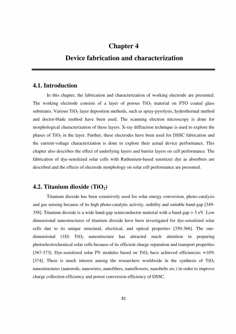
4.3.2. Deposition using the hydrothermal technique
Very thin layers of TiO2 material (50-70 nm) were deposited to be used as a seed layers in
hydrothermal process. The precursor was prepared by adding 1 mL of titanium isopropoxide to a
well-mixed solution containing 15 mL of HCl and 15 mL of H2O, and then the whole mixture
85
was vigorously stirred for another 10 min until the solution became clear. Afterward, the
precursor was poured into a Teflon-lined stainless steel autoclave with the FTO substrates placed
at an angle against the wall with the conductive side facing down (Fig. 4.2). Hydrothermal
growth was conducted at 200 °C for 3 h in an electric oven. Afterward, the FTO substrates were
rinsed with deionized water and dried in ambient air.
Figure 4.2: Schematic diagram of autoclave for deposition of TiO2 nanorods
4.3.3. Deposition by doctor-blade method
Anatase titanium (IV) oxide nanopowder having a particle size < 25 nm, 99.7% trace
metals basis (Sigma-Aldrich) was used for preparing the working electrode of DSSC. The
nanocrystalline TiO2 paste was prepared by grinding TiO2 nanopowder (12 gm) in a mortar-pestle
while adding solvent (about 20 ml acetic acid (pH adjusted to 3.5 in DI water)) dropwise. The
paste preparation was done in ambient air at room temperature. The paste obtained was mixed
with excess ethanol (150 ml) and magnetically stirred at 350 rpm for 2-4 hours. The
ultrasonication was performed for 15 minutes to homogenize TiO2 nanoparticles. The contents in
the dispersion were concentrated by evaporator at 40 °C. The DSSC working electrodes were
prepared by immersing the FTO glass plates in a 40 mM aqueous TiCl4 solution at 70 °C for 15
minutes and rinsed with DI water and ethanol. The rinsed working electrode was sintered at 450
86
°C for 30 minutes. A layer of nanocrystalline titania paste was deposited on the above FTO glass
by doctor-blade method. The developed DSSC working electrodes were placed in ethanol for a
few minutes to reduce surface irregularities, and then dried for 5 minutes at 130 °C. The samples
were sintered at 450 °C for 30 minutes in ambient air. Further, the developed nanocrystalline
TiO2 electrodes were immersed in 40 mM TiCl4 solution for 15 minutes and sintered at 450 °C
for 15 minutes.
4.3.4. Assembling of DSSC
The TiO2 working electrode was sensitized in 0.5 mM N-719 dye (Dyesol, Australia)
solution (mixture of acetonitrile and methanol, volume ratio: 1:1) at 70°C for 18-20 hours in a
dark room. Transparent platinum-coated counter electrodes with fill holes were procured from
Dyesol (MBPT-38, Dyesol, Australia). The dye-covered TiO2 electrode and Pt-coated counter
electrode were assembled in to a sandwich type cell and sealed with Surlyn (25 µm). A drop of
high-stability electrolyte (EL-HSE, Dyesol, Australia) was put in the hole in the back of the
counter electrode. Finally the hole was sealed by using a hot-melt aluminum baked Bynel-
thermoplastic sealant (Dyesol).
4.4. Characterization
4.4.1. Morphological characterization of TiO2 layer
4.4.1.1. Hydrothermally grown TiO2
A thin layer of TiO2 was obtained by spray pyrolysis, which is used as a seed layer for
further deposition of TiO2 using hydrothermal technique. The sprayed samples were
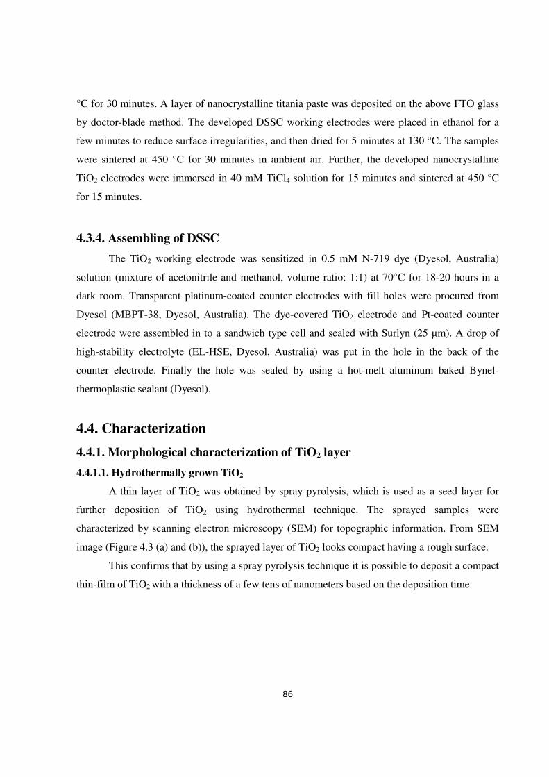
characterized by scanning electron microscopy (SEM) for topographic information. From SEM
image (Figure 4.3 (a) and (b)), the sprayed layer of TiO2 looks compact having a rough surface.
This confirms that by using a spray pyrolysis technique it is possible to deposit a compact
thin-film of TiO2 with a thickness of a few tens of nanometers based on the deposition time.
87
Figure 4.3: (a) The SEM image of sprayed TiO2 layer; (b) Magnified view of sprayed TiO2 layer
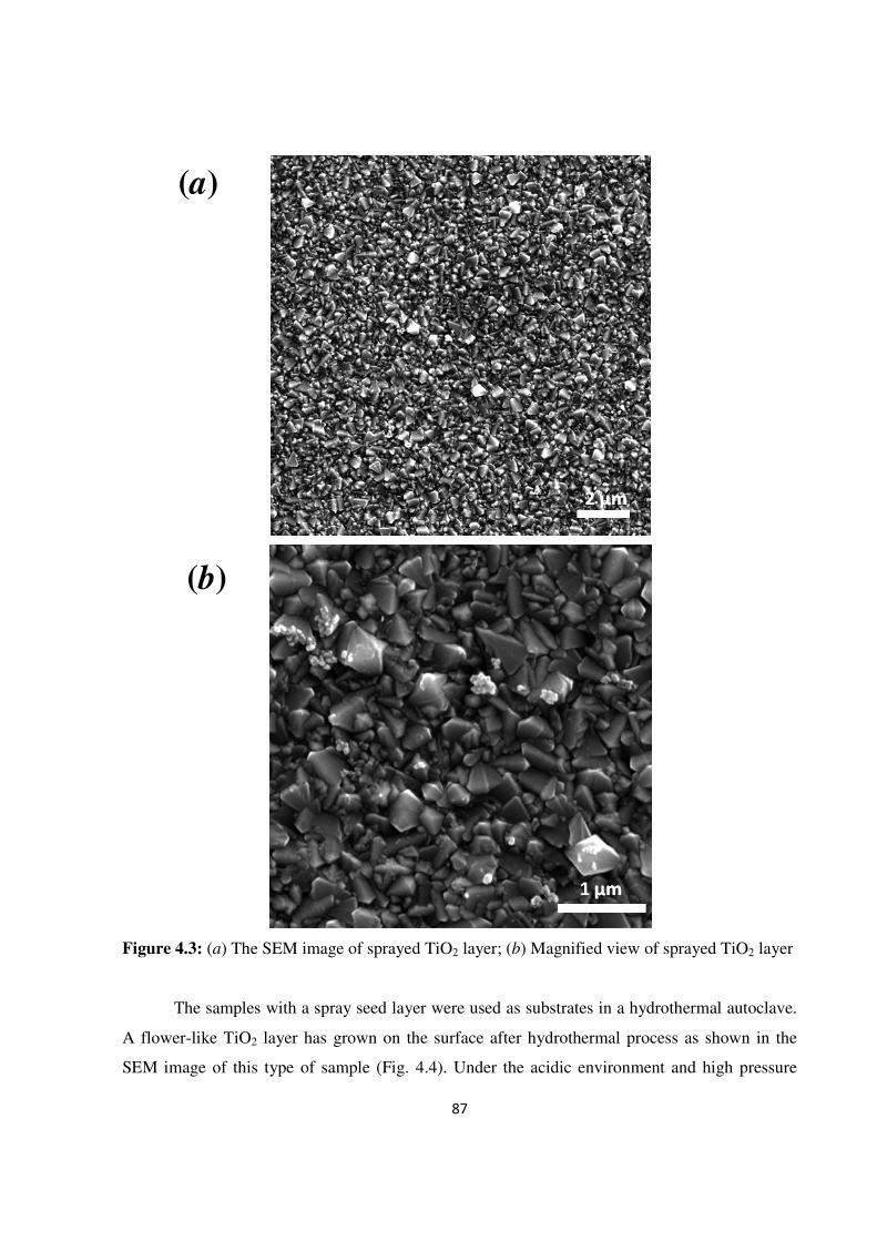
The samples with a spray seed layer were used as substrates in a hydrothermal autoclave.
A flower-like TiO2 layer has grown on the surface after hydrothermal process as shown in the
SEM image of this type of sample (Fig. 4.4). Under the acidic environment and high pressure
(a)
(b)
88
conditions of hydrothermal process (200 °C, 3 hrs), the morphology of seed layer completely
changed as shown in the Fig. 4.4 (b). From the Figure 4.4 it is observed that there is layered
structure and then the formation of TiO2 flower-like structure has happened from the one-
dimensional nano-rods. Due to changed morphology, which shows the layers are not
interconnected, this type of samples could not be used for DSSC applications. As we know the
device need interconnected particles (or grains) for better electron transport; this requirement is
not fulfilled by these samples.
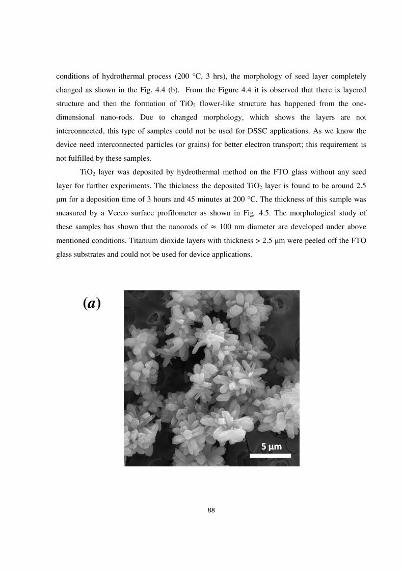
TiO2 layer was deposited by hydrothermal method on the FTO glass without any seed
layer for further experiments. The thickness the deposited TiO2 layer is found to be around 2.5
µm for a deposition time of 3 hours and 45 minutes at 200 °C. The thickness of this sample was
measured by a Veeco surface profilometer as shown in Fig. 4.5. The morphological study of
these samples has shown that the nanorods of ≈ 100 nm diameter are developed under above
mentioned conditions. Titanium dioxide layers with thickness > 2.5 µm were peeled off the FTO
glass substrates and could not be used for device applications.
(a)
89
Figure 4.4: (a) The SEM image of hydrothermally grown TiO2 flower-like structures on the FTO
glass; (b) Morphology change observed for the seed layer deposited by spray pyrolysis (this
morphology is observed between the flower-like structures)
Figure 4.5: The surface profile of the hydrothermally processed TiO2 thin film on the FTO glass
substrate
(b)
90
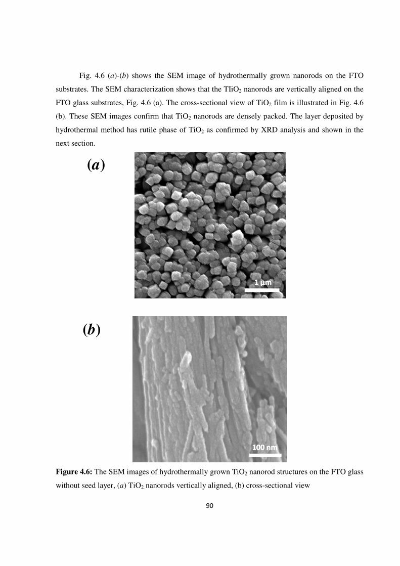
Fig. 4.6 (a)-(b) shows the SEM image of hydrothermally grown nanorods on the FTO
substrates. The SEM characterization shows that the TIiO2 nanorods are vertically aligned on the
FTO glass substrates, Fig. 4.6 (a). The cross-sectional view of TiO2 film is illustrated in Fig. 4.6
(b). These SEM images confirm that TiO2 nanorods are densely packed. The layer deposited by
hydrothermal method has rutile phase of TiO2 as confirmed by XRD analysis and shown in the
next section.
Figure 4.6: The SEM images of hydrothermally grown TiO2 nanorod structures on the FTO glass
without seed layer, (a) TiO2 nanorods vertically aligned, (b) cross-sectional view
(b)
(a)
91
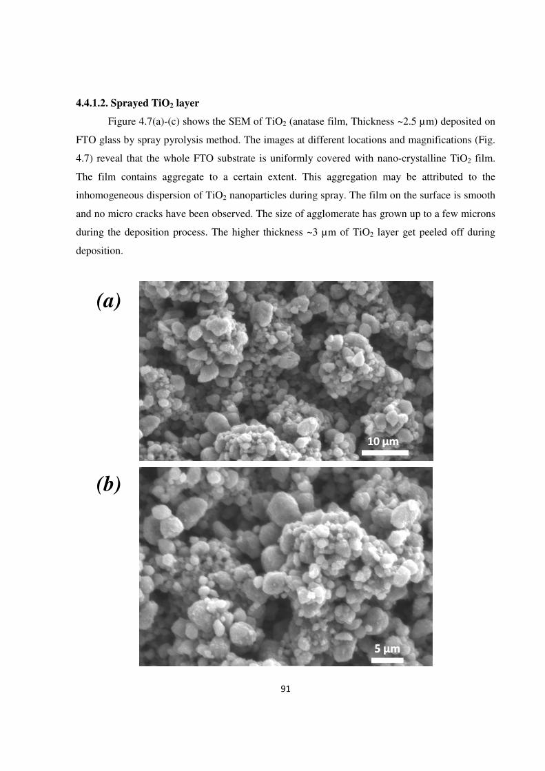
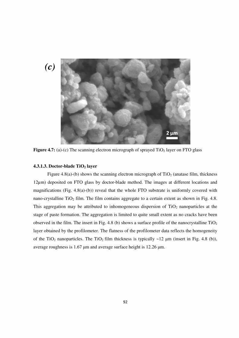
4.4.1.2. Sprayed TiO2 layer
Figure 4.7(a)-(c) shows the SEM of TiO2 (anatase film, Thickness ~2.5 µm) deposited on
FTO glass by spray pyrolysis method. The images at different locations and magnifications (Fig.
4.7) reveal that the whole FTO substrate is uniformly covered with nano-crystalline TiO2 film.
The film contains aggregate to a certain extent. This aggregation may be attributed to the
inhomogeneous dispersion of TiO2 nanoparticles during spray. The film on the surface is smooth
and no micro cracks have been observed. The size of agglomerate has grown up to a few microns
during the deposition process. The higher thickness ~3 µm of TiO2 layer get peeled off during
deposition.
(a)
(b)
92
Figure 4.7: (a)-(c) The scanning electron micrograph of sprayed TiO2 layer on FTO glass
4.3.1.3. Doctor-blade TiO2 layer
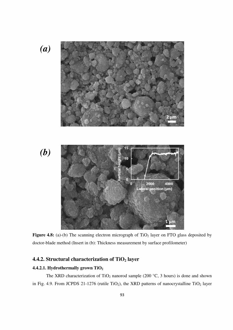
Figure 4.8(a)-(b) shows the scanning electron micrograph of TiO2 (anatase film, thickness
12µm) deposited on FTO glass by doctor-blade method. The images at different locations and
magnifications (Fig. 4.8(a)-(b)) reveal that the whole FTO substrate is uniformly covered with
nano-crystalline TiO2 film. The film contains aggregate to a certain extent as shown in Fig. 4.8.
This aggregation may be attributed to inhomogeneous dispersion of TiO2 nanoparticles at the
stage of paste formation. The aggregation is limited to quite small extent as no cracks have been
observed in the film. The insert in Fig. 4.8 (b) shows a surface profile of the nanocrystalline TiO2
layer obtained by the profilometer. The flatness of the profilometer data reflects the homogeneity
of the TiO2 nanoparticles. The TiO2 film thickness is typically ~12 µm (insert in Fig. 4.8 (b)),
average roughness is 1.67 µm and average surface height is 12.26 µm.
(c)
93
Figure 4.8: (a)-(b) The scanning electron micrograph of TiO2 layer on FTO glass deposited by
doctor-blade method (Insert in (b): Thickness measurement by surface profilometer)
4.4.2. Structural characterization of TiO2 layer
4.4.2.1. Hydrothermally grown TiO2
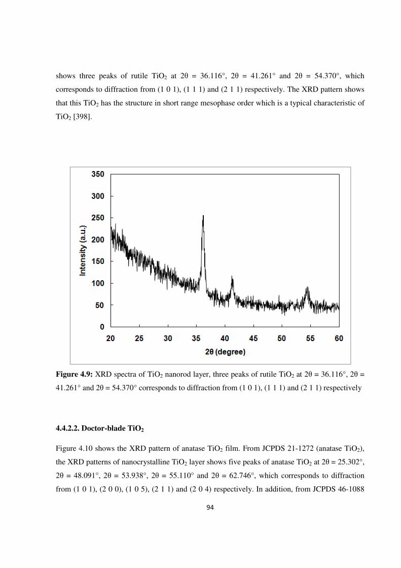
The XRD characterization of TiO2 nanorod sample (200 °C, 3 hours) is done and shown
in Fig. 4.9. From JCPDS 21-1276 (rutile TiO2), the XRD patterns of nanocrystalline TiO2 layer
(a)
(b)
94
shows three peaks of rutile TiO2 at 2θ = 36.116°, 2θ = 41.261° and 2θ = 54.370°, which
corresponds to diffraction from (1 0 1), (1 1 1) and (2 1 1) respectively. The XRD pattern shows
that this TiO2 has the structure in short range mesophase order which is a typical characteristic of
TiO2 [398].
Figure 4.9: XRD spectra of TiO2 nanorod layer, three peaks of rutile TiO2 at 2θ = 36.116°, 2θ =
41.261° and 2θ = 54.370° corresponds to diffraction from (1 0 1), (1 1 1) and (2 1 1) respectively
4.4.2.2. Doctor-blade TiO2
Figure 4.10 shows the XRD pattern of anatase TiO2 film. From JCPDS 21-1272 (anatase TiO2),
the XRD patterns of nanocrystalline TiO2 layer shows five peaks of anatase TiO2 at 2θ = 25.302°,
2θ = 48.091°, 2θ = 53.938°, 2θ = 55.110° and 2θ = 62.746°, which corresponds to diffraction
from (1 0 1), (2 0 0), (1 0 5), (2 1 1) and (2 0 4) respectively. In addition, from JCPDS 46-1088
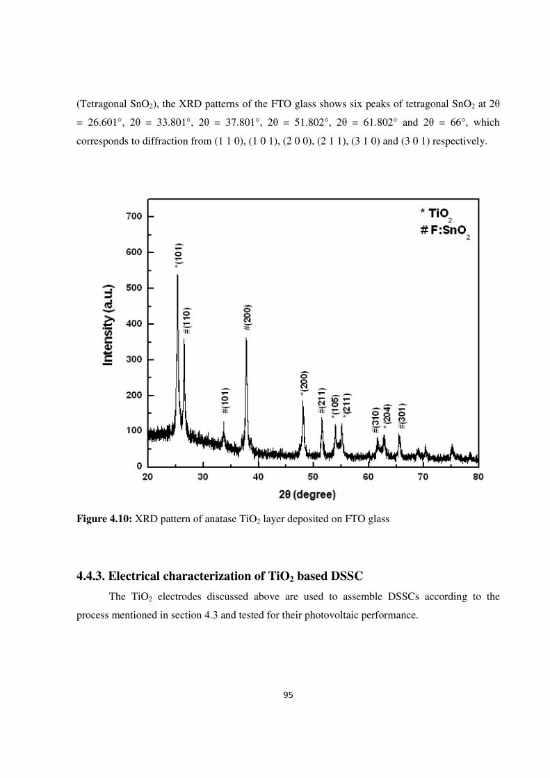
95
(Tetragonal SnO2), the XRD patterns of the FTO glass shows six peaks of tetragonal SnO2 at 2θ
= 26.601°, 2θ = 33.801°, 2θ = 37.801°, 2θ = 51.802°, 2θ = 61.802° and 2θ = 66°, which
corresponds to diffraction from (1 1 0), (1 0 1), (2 0 0), (2 1 1), (3 1 0) and (3 0 1) respectively.
Figure 4.10: XRD pattern of anatase TiO2 layer deposited on FTO glass
4.4.3. Electrical characterization of TiO2 based DSSC
The TiO2 electrodes discussed above are used to assemble DSSCs according to the
process mentioned in section 4.3 and tested for their photovoltaic performance.
96
4.4.3.1. Hydrothermal TiO2 sample
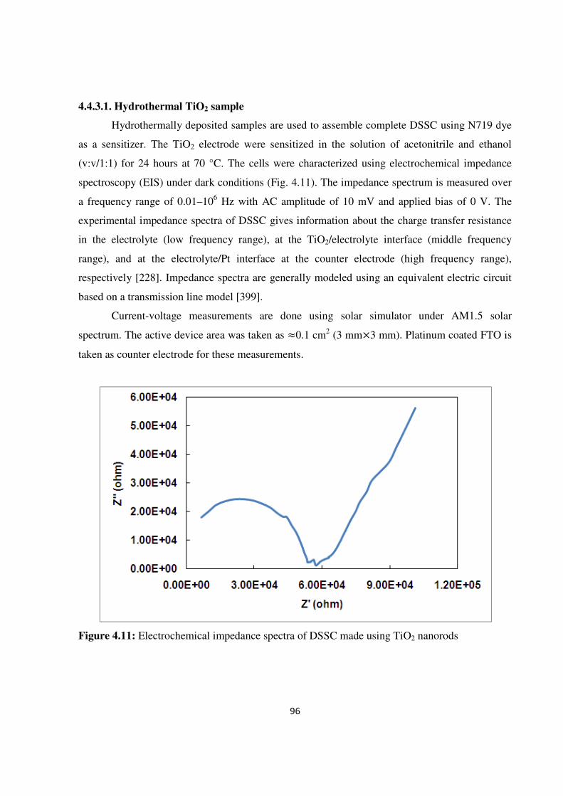
Hydrothermally deposited samples are used to assemble complete DSSC using N719 dye
as a sensitizer. The TiO2 electrode were sensitized in the solution of acetonitrile and ethanol
(v:v/1:1) for 24 hours at 70 °C. The cells were characterized using electrochemical impedance
spectroscopy (EIS) under dark conditions (Fig. 4.11). The impedance spectrum is measured over
a frequency range of 0.01–106 Hz with AC amplitude of 10 mV and applied bias of 0 V. The
experimental impedance spectra of DSSC gives information about the charge transfer resistance
in the electrolyte (low frequency range), at the TiO2/electrolyte interface (middle frequency
range), and at the electrolyte/Pt interface at the counter electrode (high frequency range),
respectively [228]. Impedance spectra are generally modeled using an equivalent electric circuit
based on a transmission line model [399].
Current-voltage measurements are done using solar simulator under AM1.5 solar
spectrum. The active device area was taken as ≈0.1 cm2 (3 mm×3 mm). Platinum coated FTO is
taken as counter electrode for these measurements.
Figure 4.11: Electrochemical impedance spectra of DSSC made using TiO2 nanorods
97
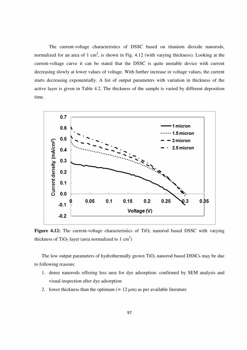
The current-voltage characteristics of DSSC based on titanium dioxide nanorods,
normalized for an area of 1 cm2, is shown in Fig. 4.12 (with varying thickness). Looking at the
current-voltage curve it can be stated that the DSSC is quite unstable device with current
decreasing slowly at lower values of voltage. With further increase in voltage values, the current
starts decreasing exponentially. A list of output parameters with variation in thickness of the
active layer is given in Table 4.2. The thickness of the sample is varied by different deposition
time.
Figure 4.12: The current-voltage characteristics of TiO2 nanorod based DSSC with varying
thickness of TiO2 layer (area normalized to 1 cm2)
The low output parameters of hydrothermally grown TiO2 nanorod based DSSCs may be due
to following reasons:
1. dense nanorods offering less area for dye adsorption: confirmed by SEM analysis and
visual inspection after dye adsorption
2. lower thickness than the optimum (≈ 12 µm) as per available literature
98
3. large series resistance: there may be a dense thicker layer between nanorods and
conducting surface of FTO
Further, another method for TiO2 deposition, namely spray-pyrolysis has been tried out.
Table 4.2: The output parameters of TiO2 nanorod (NR) layer based DSSC and their dependence
on thickness (given in µm)
Sample description JSC
(mA/cm2)
VOC (V) FF (%) η (%)
DSSC-H1 (TiO2 NR (1.0 µm)/N719 dye) 0.29 0.265 37.5 0.03
DSSC-H2 (TiO2 NR (1.5 µm)/N719 dye) 0.48 0.302 34.3 0.05
DSSC-H3 (TiO2 NR (2.0 µm)/N719 dye) 0.53 0.298 34.7 0.055
DSSC-H4 (TiO2 NR (2.5 µm)/N719 dye) 0.61 0.296 32.3 0.06
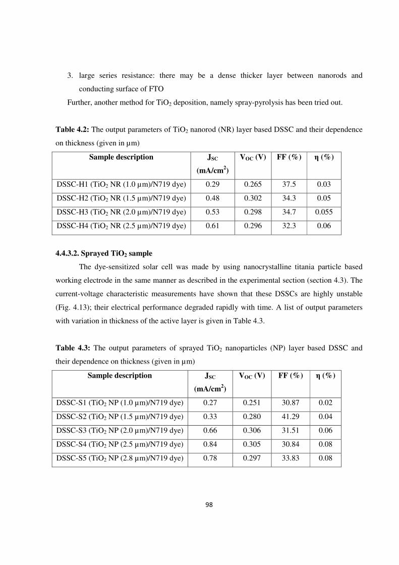
4.4.3.2. Sprayed TiO2 sample
The dye-sensitized solar cell was made by using nanocrystalline titania particle based
working electrode in the same manner as described in the experimental section (section 4.3). The
current-voltage characteristic measurements have shown that these DSSCs are highly unstable
(Fig. 4.13); their electrical performance degraded rapidly with time. A list of output parameters
with variation in thickness of the active layer is given in Table 4.3.
Table 4.3: The output parameters of sprayed TiO2 nanoparticles (NP) layer based DSSC and
their dependence on thickness (given in µm)
Sample description JSC
(mA/cm2)
VOC (V) FF (%) η (%)
DSSC-S1 (TiO2 NP (1.0 µm)/N719 dye) 0.27 0.251 30.87 0.02
DSSC-S2 (TiO2 NP (1.5 µm)/N719 dye) 0.33 0.280 41.29 0.04
DSSC-S3 (TiO2 NP (2.0 µm)/N719 dye) 0.66 0.306 31.51 0.06
DSSC-S4 (TiO2 NP (2.5 µm)/N719 dye) 0.84 0.305 30.84 0.08
DSSC-S5 (TiO2 NP (2.8 µm)/N719 dye) 0.78 0.297 33.83 0.08
99
Figure 4.13: The current-voltage characteristics of DSSC
The low output parameters of sprayed TiO2 nanoparticle based DSSCs may be due to
following reasons:
1. dense nanoparticles growing as big agglomerate offering less area for dye adsorption:
confirmed by SEM analysis
2. lower thickness than the optimum (≈ 12 µm) as per available literature
3. low shunt resistance: short-circuit path may be available through nanospace among the
bigger agglomerates
4. higher recombination as seen in a sharp decrease of current at lower voltage [400]
5. the large series resistance offered by FTO
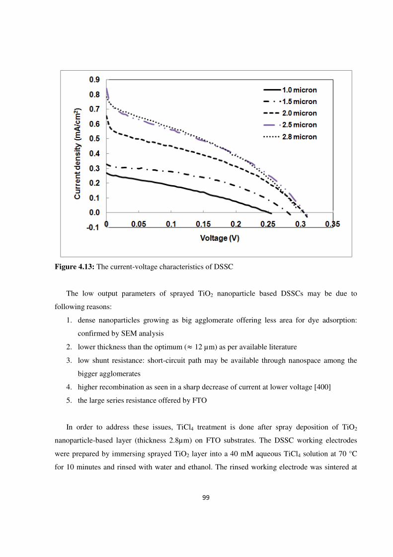
In order to address these issues, TiCl4 treatment is done after spray deposition of TiO2
nanoparticle-based layer (thickness 2.8µm) on FTO substrates. The DSSC working electrodes
were prepared by immersing sprayed TiO2 layer into a 40 mM aqueous TiCl4 solution at 70 °C
for 10 minutes and rinsed with water and ethanol. The rinsed working electrode was sintered at
100
450 °C for 15 minutes. The current-voltage characteristic of this sample is shown in Fig. 4.14 and
corresponding output parameters are listed in Table 4.4.
Figure 4.14: The current-voltage characteristics of DSSC developed using sprayed TiO2 layer
Table 4.4: The output parameters of DSSC fabricated using TiCl4-treated sprayed TiO2 layer
Sample description JSC (mA/cm2) VOC (V) FF (%) η (%)
DSSC-S6 (TiO2 NP (3 µm)/N719 dye) 4.89 0.673 28.1 0.92
This improvement in performance due to TiCl4 treatment is attributed to better dye absorption
and relaxing of TiO2 defects. In literature, improvements in photon-to-current conversion
efficiencies of DSSCs using TiCl4-treated TiO2 films were attributed to enhanced film thickness
and light scattering [401]. Further, the luminescence measurements reported in the literature
provide experimental evidence that TiCl4 treatment suppresses surface defect states that are likely
to be associated with oxygen vacancies [402].
There is significant improvement in photovoltaic performance of spray deposited thin films
as compared to hydrothermally prepared, further improve is restricted in spray deposited films

101
due to pealing of films at higher thickness (> 3µm). So to get higher thickness films, well known
doctor blade method is adopted for further study.
4.4.3.3. Doctor-blade TiO2 layer
Electrical characterization for DSSC based on doctor-blade TiO2 layer is presented in Fig.
4.15. A list of output parameters with variation in thickness of TiO2 layer is given in Table 4.5.
Table 4.5: The output parameters of doctor-blade made TiO2 layer based DSSC and their
dependence on thickness (given in µm)
Sample description JSC (mA/cm2) VOC (V) FF (%) η (%)
DSSC-D1 (TiO2 NP (10 µm)/N719 dye) 13.02 0.613 19.54 1.56
DSSC-D2 (TiO2 NP (11 µm)/N719 dye) 13.85 0.616 17.61 1.50
Figure 4.15: The current-voltage characteristics of DSSC developed using doctor-blade TiO2
layer
102
The low fill factor and efficiencies of doctor-blade made TiO2 nanoparticle layer based
DSSCs may be due to following reasons:
1. low shunt resistance: short-circuit path may be available through nanospace among the
agglomerates
2. large series resistance
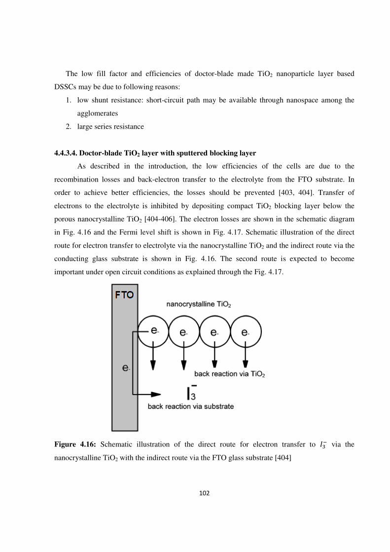
4.4.3.4. Doctor-blade TiO2 layer with sputtered blocking layer
As described in the introduction, the low efficiencies of the cells are due to the
recombination losses and back-electron transfer to the electrolyte from the FTO substrate. In
order to achieve better efficiencies, the losses should be prevented [403, 404]. Transfer of
electrons to the electrolyte is inhibited by depositing compact TiO2 blocking layer below the
porous nanocrystalline TiO2 [404-406]. The electron losses are shown in the schematic diagram
in Fig. 4.16 and the Fermi level shift is shown in Fig. 4.17. Schematic illustration of the direct
route for electron transfer to electrolyte via the nanocrystalline TiO2 and the indirect route via the
conducting glass substrate is shown in Fig. 4.16. The second route is expected to become
important under open circuit conditions as explained through the Fig. 4.17.
Figure 4.16: Schematic illustration of the direct route for electron transfer to via the
nanocrystalline TiO2 with the indirect route via the FTO glass substrate [404]
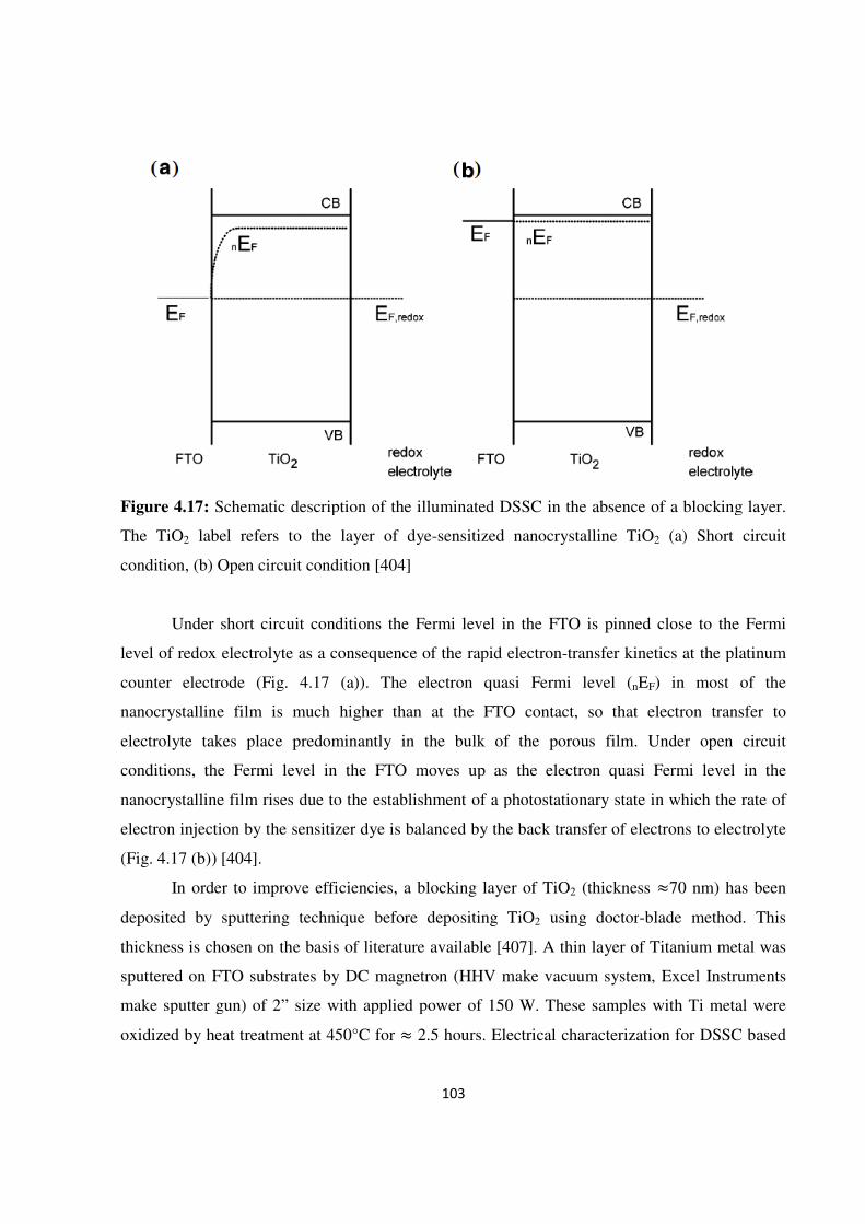
Figure 4.17: Schematic description of the illuminated DSSC in the
The TiO2 label refers to the layer of dye
condition, (b) Open circuit condition
Under short circuit conditions the Fermi level in the FTO is
level of redox electrolyte as a consequence of the rapid electron
counter electrode (Fig. 4.1
nanocrystalline film is much higher than at the FTO contact, so
electrolyte takes place predominantly in the bulk of the porous film. Under open circuit
conditions, the Fermi level in the FTO moves up as the electron quasi Fermi level in the
nanocrystalline film rises due to the establishment of a photostationary state in which the rate of
electron injection by the sensitizer dye is balance
(Fig. 4.17 (b)) [404].
In order to improve efficiencies,
deposited by sputtering technique before
thickness is chosen on the basis of literature available
sputtered on FTO substrates
make sputter gun) of 2” size with applied power of 150 W
oxidized by heat treatment at 450°C for
103
Schematic description of the illuminated DSSC in the absence of a blocking layer.
label refers to the layer of dye-sensitized nanocrystalline TiO
pen circuit condition [404]
Under short circuit conditions the Fermi level in the FTO is pinned
as a consequence of the rapid electron-transfer kinetics at the platinum
(Fig. 4.17 (a)). The electron quasi Fermi level (
nanocrystalline film is much higher than at the FTO contact, so
takes place predominantly in the bulk of the porous film. Under open circuit
ons, the Fermi level in the FTO moves up as the electron quasi Fermi level in the
nanocrystalline film rises due to the establishment of a photostationary state in which the rate of
electron injection by the sensitizer dye is balanced by the back transfer of electrons to
In order to improve efficiencies, a blocking layer of TiO2 (thickness
deposited by sputtering technique before depositing TiO2 using doctor
thickness is chosen on the basis of literature available [407]. A thin layer of Titanium metal was
on FTO substrates by DC magnetron (HHV make vacuum system, Excel Instruments
make sputter gun) of 2” size with applied power of 150 W. These samples with Ti metal were
oxidized by heat treatment at 450°C for ≈ 2.5 hours. Electrical characterization for DSSC based
absence of a blocking layer.
nanocrystalline TiO2 (a) Short circuit
pinned close to the Fermi
transfer kinetics at the platinum
. The electron quasi Fermi level (nEF) in most of the
nanocrystalline film is much higher than at the FTO contact, so that electron transfer to
takes place predominantly in the bulk of the porous film. Under open circuit
ons, the Fermi level in the FTO moves up as the electron quasi Fermi level in the
nanocrystalline film rises due to the establishment of a photostationary state in which the rate of
by the back transfer of electrons to electrolyte
(thickness ≈70 nm) has been
using doctor-blade method. This
A thin layer of Titanium metal was
by DC magnetron (HHV make vacuum system, Excel Instruments
samples with Ti metal were
Electrical characterization for DSSC based
104
on doctor-blade TiO2 layer along with the blocking layer is presented in Fig. 4.18. A list of output
parameters with variation in thickness of TiO2 layer is given in Table 4.6.
Table 4.6: The output parameters DSSC fabricated from doctor-blade made TiO2 layer on
blocking layer and their dependence on thickness (given in µm)
Sample description JSC (mA/cm2) VOC (V) FF (%) η (%)
DSSC-D-B1 (TiO2 NP (7 µm)/N719 dye) 1.68 0.660 45.24 0.50
DSSC-D-B2 (TiO2 NP (10 µm)/N719 dye) 3.64 0.678 36.21 0.89
DSSC-D-B3 (TiO2 NP (12 µm)/N719 dye) 5.29 0.702 35.9 1.33
Figure 4.18: The current-voltage characteristics of DSSC developed using doctor-blade TiO2
layer
As expected the blocking layer has reduced short-circuit current density, but at the same
time, the fill factor has improved. So it can be concluded from these experiments that blocking
105
layer reduces nanospace in between the agglomerate and conducting FTO substrates. The results
are in accordance with the literature [406].
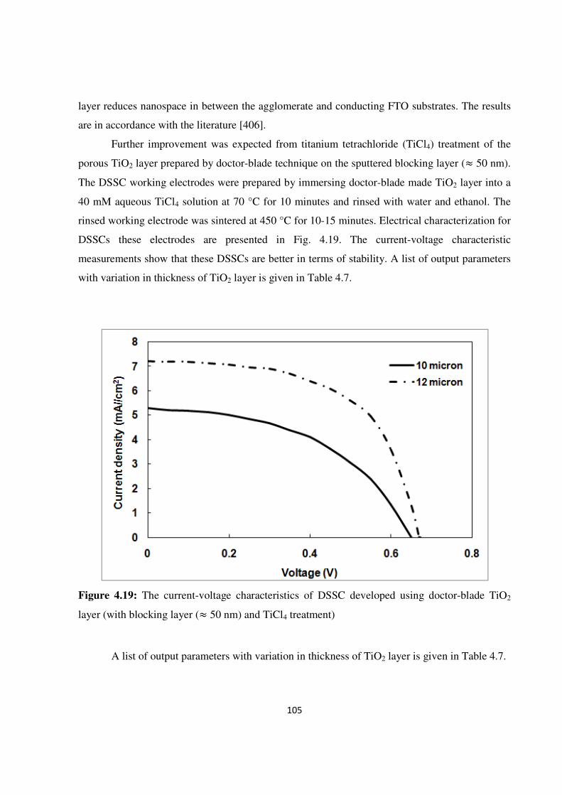
Further improvement was expected from titanium tetrachloride (TiCl4) treatment of the
porous TiO2 layer prepared by doctor-blade technique on the sputtered blocking layer (≈ 50 nm).
The DSSC working electrodes were prepared by immersing doctor-blade made TiO2 layer into a
40 mM aqueous TiCl4 solution at 70 °C for 10 minutes and rinsed with water and ethanol. The
rinsed working electrode was sintered at 450 °C for 10-15 minutes. Electrical characterization for
DSSCs these electrodes are presented in Fig. 4.19. The current-voltage characteristic
measurements show that these DSSCs are better in terms of stability. A list of output parameters
with variation in thickness of TiO2 layer is given in Table 4.7.
Figure 4.19: The current-voltage characteristics of DSSC developed using doctor-blade TiO2
layer (with blocking layer (≈ 50 nm) and TiCl4 treatment)
A list of output parameters with variation in thickness of TiO2 layer is given in Table 4.7.
106
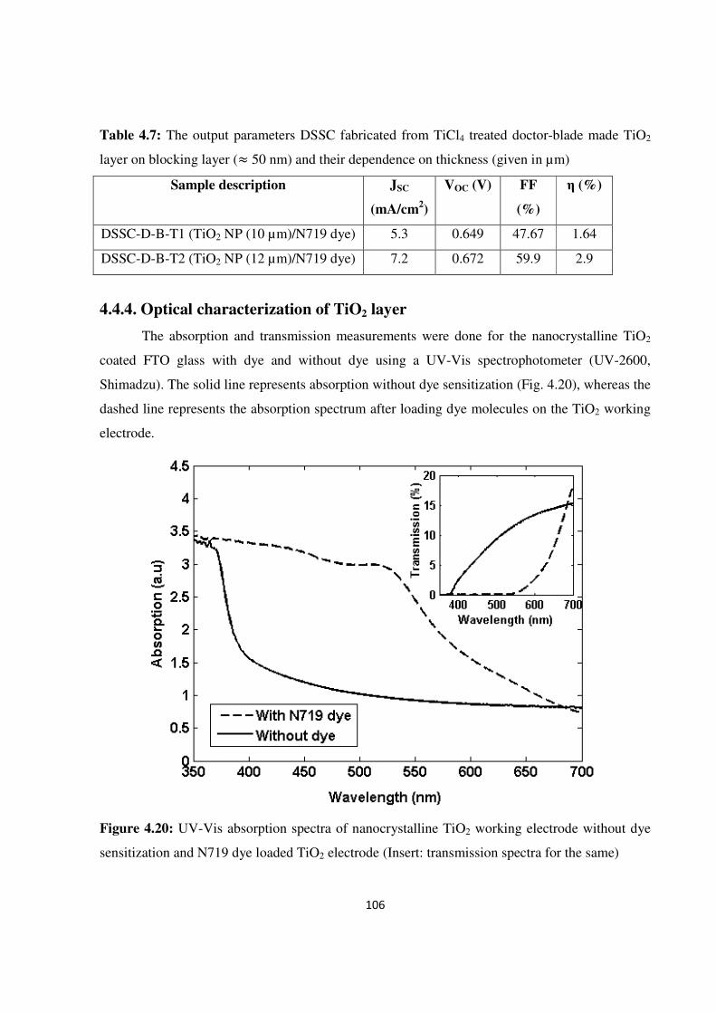
Table 4.7: The output parameters DSSC fabricated from TiCl4 treated doctor-blade made TiO2
layer on blocking layer (≈ 50 nm) and their dependence on thickness (given in µm)
Sample description JSC
(mA/cm2)
VOC (V) FF
(%)
η (%)
DSSC-D-B-T1 (TiO2 NP (10 µm)/N719 dye) 5.3 0.649 47.67 1.64
DSSC-D-B-T2 (TiO2 NP (12 µm)/N719 dye) 7.2 0.672 59.9 2.9
4.4.4. Optical characterization of TiO2 layer
The absorption and transmission measurements were done for the nanocrystalline TiO2
coated FTO glass with dye and without dye using a UV-Vis spectrophotometer (UV-2600,
Shimadzu). The solid line represents absorption without dye sensitization (Fig. 4.20), whereas the
dashed line represents the absorption spectrum after loading dye molecules on the TiO2 working
electrode.
Figure 4.20: UV-Vis absorption spectra of nanocrystalline TiO2 working electrode without dye
sensitization and N719 dye loaded TiO2 electrode (Insert: transmission spectra for the same)
107
Figure 4.20 illustrates that light absorption increases in the 400-700 nm wavelength range
for a dye-sensitized TiO2 electrode compared to that for a bare TiO2 working electrode. The
absorption peak is observed at ~520 nm, which is a characteristic of N719 dye. The insert shows
transmission spectra of bare nanocrystalline TiO2 working electrode and N719 dye-loaded TiO2
electrode (Fig. 4.20). The TiO2 nanoparticle layer was hazy and whitish in nature. The incident
light below 380 nm is absorbed by the band-to-band absorption. The transmission curve shifts
downward when the TiO2 electrode is dye-sensitized, due to absorbing nature of dye molecules in
the visible range.
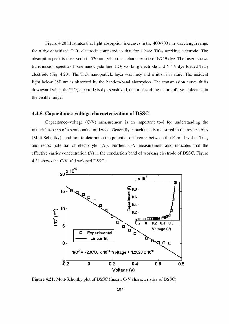
4.4.5. Capacitance-voltage characterization of DSSC
Capacitance–voltage (C-V) measurement is an important tool for understanding the
material aspects of a semiconductor device. Generally capacitance is measured in the reverse bias
(Mott-Schottky) condition to determine the potential difference between the Fermi level of TiO2
and redox potential of electrolyte (Vbi). Further, C-V measurement also indicates that the
effective carrier concentration (N) in the conduction band of working electrode of DSSC. Figure
4.21 shows the C-V of developed DSSC.
Figure 4.21: Mott-Schottky plot of DSSC (Insert: C-V characteristics of DSSC)
108
The slope and its intersection on the abscissa in the Mott-Schottky plot shown in Fig.
4.21 for the DSSC, gives the carrier concentration (N) under dark conditions and the potential
difference (Vbi) respectively. A linear fit was performed on the experimental data obtained to
explore the charge carrier density and barrier potential. The N value is calculated as ≈1011
cm-3
and the value of Vbi - 2 kT/q is equal to 0.6 eV, which corresponds to Vbi = 0.55 eV. The
magnitude of charge carrier density is in agreement with the insulating nature of TiO2 material
under dark conditions.
The experimental non-linear plot of C-2 versus V (Fig. 4.20) results from the surface state
effects, recombination effects and non-negligible contributions of the Helmhotz layer to the
interfacial capacitance. The insert in Fig. 4.21 shows an increase in the capacitance of DSSC with
increasing bias voltage, which is in agreement with existing literature [280].
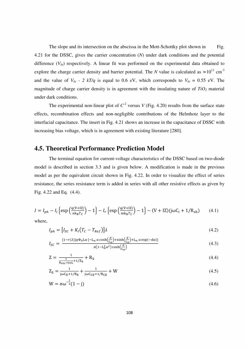
4.5. Theoretical Performance Prediction Model
The terminal equation for current-voltage characteristics of the DSSC based on two-diode
model is described in section 3.3 and is given below. A modification is made in the previous
model as per the equivalent circuit shown in Fig. 4.22. In order to visualize the effect of series
resistance, the series resistance term is added in series with all other resistive effects as given by
Fig. 4.22 and Eq. (4.4).
= − exp ()
− 1 − exp ()!
− 1 − (V + IZ)(jωC) + 1/R,-) (4.1)
where,
= ./0 + 12340 − 456789: (4.2)
/0 = [= (>)]@ABCD [CE D FG,- H
IE,)- H
IECE D JKL(MD)]
N3=COP DP8 FG,- QIE
(4.3)
Z = =R
STUVWXYI=/Z+ R[ (4.4)
Z[ = =\]^_=/`_
+ =\]^a_=/`a_
+ W (4.5)
W = σωRP(1 − j) (4.6)
109
Figure 4.22: The equivalent circuit of the DSSC
A short description of the dynamic resistance prediction model is given below. The
detailed treatment is given in section 3.3. The equation (4.1) can be modified under static
condition (ω ≈ 0) as given below:
= − exp ()ea
− 1 − exp ()!ea
− 1 − ((V + IZ)/R,-) (4.7)
In order to estimate the dynamic resistance, Eq. (4.7) is subjected to following boundary
conditions:
(i) 0 < V < Vm and Im < I < ISC
(ii) Vm< V < VOC and 0 < I < Im
At any two operating points (V1, I1) and (Vm, Im) on a single I-V curve, the relationships
between V and I are:
V= = !ea × ln `hi.ji2k2lR9R
`hi2l− I=Z (4.8)
V! = !ea × ln `hi.ji2k2lm9m
`hi2l− I!Z (4.9)
At any two operating points (Vm, Im) and (V2, I2) on a single I-V curve, the relationship
between V and I are:
V! = ea × ln `hi.ji2k2lm9m
`hi2l− I!Z (4.10)
Vn = ea × ln `hi.ji2k2lP9P
`hi2l− InZ (4.11)
Since a shunt resistance is normally much greater than series impedance Z. Thus
R,-.IL- + + − I=9>>I=Z and R,-.IL- + + − In9>>InZ. Therefore,
110
o = pRpP2P2R
− (!)ea × ln .ji2k2lR9
.ji2k2lP9 (4.12)
The first term of Eq. (4.12) is essentially a slope at any operating point, or the external
dynamic resistance, RD. The second term is the internal dynamic resistance, Rd of the DSSC.
4.6. Validation and analysis of the model developed
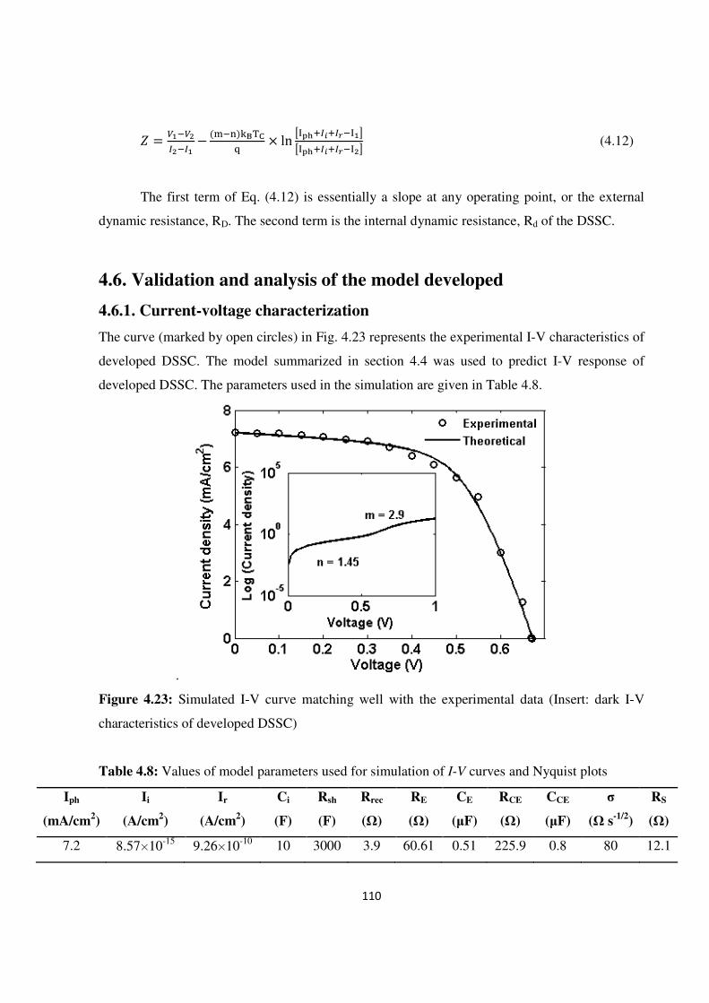
4.6.1. Current-voltage characterization
The curve (marked by open circles) in Fig. 4.23 represents the experimental I-V characteristics of
developed DSSC. The model summarized in section 4.4 was used to predict I-V response of
developed DSSC. The parameters used in the simulation are given in Table 4.8.
.
Figure 4.23: Simulated I-V curve matching well with the experimental data (Insert: dark I-V
characteristics of developed DSSC)
Table 4.8: Values of model parameters used for simulation of I-V curves and Nyquist plots
Iph
(mA/cm2)
Ii
(A/cm2)
Ir
(A/cm2)
Ci
(F)
Rsh
(F)
Rrec
(Ω)
RE
(Ω)
CE
(µF)
RCE
(Ω)
CCE
(µF)
σ
(Ω s-1/2
)
RS
(Ω)
7.2 8.57×10⁻¹⁵
9.26×10⁻¹⁰
10 3000 3.9 60.61 0.51 225.9 0.8 80 12.1
111
It is evident from Fig. 4.23 that the theoretical model given in section 4.5 agrees quite
well with the experimental data. The experimentally observed cell efficiency of 2.9% (JSC = 7.2
mA/cm2; VOC = 672 mV; PMAX = 2.9 mW; FF = 59.9%; RS = 22 Ω) is in good agreement with the
simulated parameters of a DSSC having efficiency of 2.9% (JSC = 7.2 mA/cm2; VOC = 672.5 mV;
PMAX = 2.9 mW; FF = 59.89%; RS = 22.2 Ω). The experimental and simulated I-V curves were
fitted by means of the parameters RS, Rsh, Di and Dr. The insert in Fig. 4.23 represents the dark I-
V characteristics of the DSSC. The fitted ideality factor reflects a combination of recombination
and diffusion currents where the n > 2 corresponds to the dominance of recombination current,
which signifies non-ideal behavior in the I-V characteristics. The non-ideality causes the
limitation of the photocurrent generated in the solar cell by diffusion of iodide-triiodide ion
within nanocrystalline TiO2 layer.
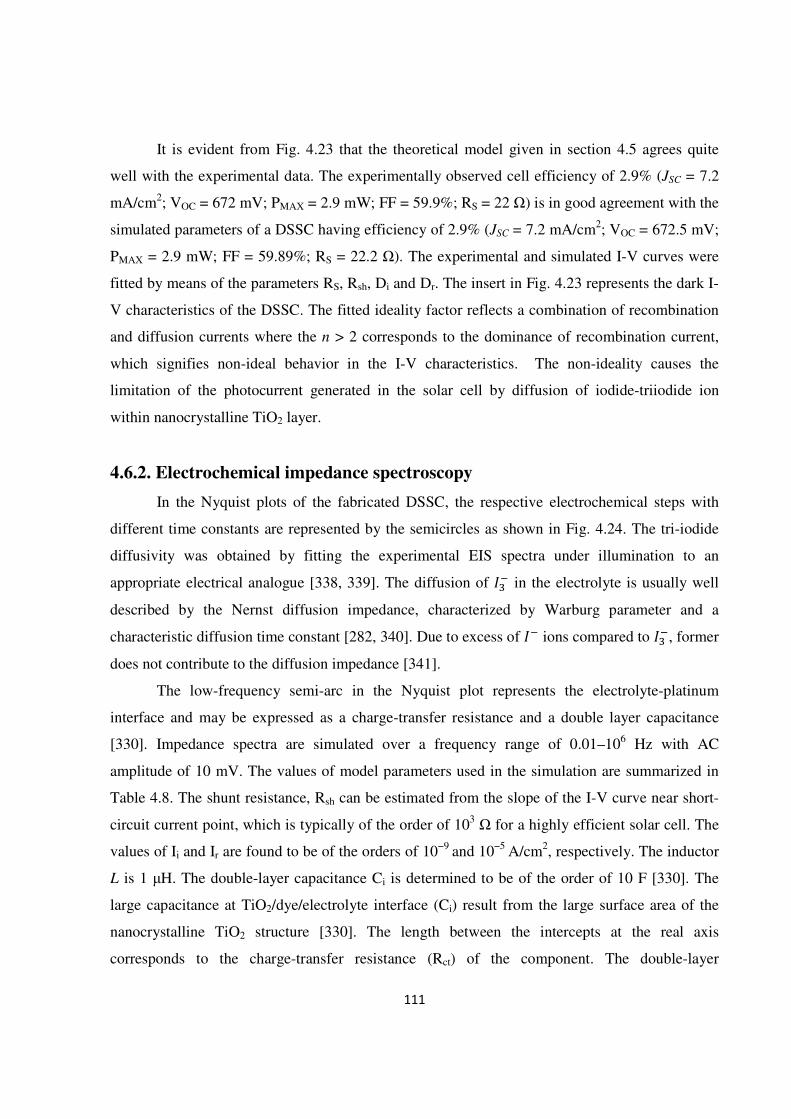
4.6.2. Electrochemical impedance spectroscopy
In the Nyquist plots of the fabricated DSSC, the respective electrochemical steps with
different time constants are represented by the semicircles as shown in Fig. 4.24. The tri-iodide
diffusivity was obtained by fitting the experimental EIS spectra under illumination to an
appropriate electrical analogue [338, 339]. The diffusion of in the electrolyte is usually well
described by the Nernst diffusion impedance, characterized by Warburg parameter and a
characteristic diffusion time constant [282, 340]. Due to excess of ions compared to , former
does not contribute to the diffusion impedance [341].
The low-frequency semi-arc in the Nyquist plot represents the electrolyte-platinum
interface and may be expressed as a charge-transfer resistance and a double layer capacitance
[330]. Impedance spectra are simulated over a frequency range of 0.01–106 Hz with AC
amplitude of 10 mV. The values of model parameters used in the simulation are summarized in
Table 4.8. The shunt resistance, Rsh can be estimated from the slope of the I-V curve near short-
circuit current point, which is typically of the order of 103 Ω for a highly efficient solar cell. The
values of Ii and Ir are found to be of the orders of 10−9
and 10−5
A/cm2, respectively. The inductor
L is 1 µH. The double-layer capacitance Ci is determined to be of the order of 10 F [330]. The
large capacitance at TiO2/dye/electrolyte interface (Ci) result from the large surface area of the
nanocrystalline TiO2 structure [330]. The length between the intercepts at the real axis
corresponds to the charge-transfer resistance (Rct) of the component. The double-layer
112
capacitance (q) is determined from the characteristic frequency, q = (rstuvwx)= [345]. The
resistance elements Rrec, RE, RCE, and RS are typically several ohms for a highly efficient solar
cell. The interfacial capacitances CE and CCE are of the orders of 1 mF and 1 µF, respectively.
Figure 4.24: The EIS of simulated DSSC matches well with experimental data
4.6.3. Effect of illumination on steady and dynamic parameters
The model proposed in section 4.4 is used to estimate the I-V characteristics of the DSSC.
The static parameters (ISC, VOC, PMAX and RS) of the fabricated DSSC are estimated under STC
conditions. The simulated current-voltage characteristics of the fabricated DSSC are shown in
Fig. 4.25 as a function of incident illumination at constant cell temperature.
The values of the dynamic resistance at MPP are computed using the values of Iph, ISC and
RS. The dynamic resistance of DSSC cell is calculated in an effective manner using a
mathematical model given in section 3.3, and reported in Table 4.9. From the data given in Table
4.9, the series resistance, RS shows a decreasing trend (from 77.8 Ω to 22.2 Ω) continuously with
increase in the intensity of illumination. The dynamic resistance is calculated from the theoretical
model for various illumination levels as listed in Table 4.9. It is found that the dynamic resistance
of fabricated DSSC decreases from 440.7 Ω to 78.6 Ω with an increase in illumination level from
20 mW/m2 to 100 mW/m
2.

113
Figure 4.25: Effect of illumination on the I-V characteristics of DSSC
Table 4.9: Effect of illumination on steady state and dynamic parameters of DSSC calculated at
298.14 K
Illumination
(mW/cm2)
JSC
(mA/cm2)
VOC
(mV)
PMAX
(mW)
RS
(Ω)
Rd
(Ω)
Efficiency,
η (%)
Ii
(A/cm2)
Ir
(A/cm2)
20 1.4 585.0 0.41 77.8 440.7 2.03 8.57×10⁻¹⁵
9.26×10⁻¹⁰
40 2.9 628.6 1.00 38.2 223.8 2.50 8.57×10⁻¹⁵
9.26×10⁻¹⁰
60 4.3 649.0 1.70 28.8 152.7 2.83 8.57×10⁻¹⁵
9.26×10⁻¹⁰
80 5.8 662.5 2.30 24.7 109.2 2.87 8.57×10⁻¹⁵ 9.26×10⁻¹⁰
100 7.2 672.5 2.90 22.2 78.6 2.90 8.57×10⁻¹⁵
9.26×10⁻¹⁰
The short-circuit current density (JSC) increases from 1.4 to 7.2 mA/cm2 with an increase
in illumination level from 20 mW/m2 to 100 mW/m
2. A logarithmic dependence of VOC (changes
from 585 mV to 672.5 mV) on the illumination is observed in the DSSC and shown in Fig. 4.25.
The dependence of VOC on the illumination (:) is given by [347]:

114
yz0α |@ ln (:) (4.13)
A detailed discussion for dependence of JSC and VOC on illumination is given in section 3.3. The
open-circuit voltage is also dependent on the saturation current density of the recombination
diode and described in section 3.3.
4.6.4. Effect of temperature on steady-state and dynamic parameters
Figure 4.26 shows the effect of cell temperature (TC) on I-V characteristics of DSSC. The
steady-state and dynamic parameters are estimated from the proposed model at different
temperatures and are listed in Table 4.10.
Table 4.10: Effect of temperature on steady state and dynamic parameters of DSSC at 100
mWcmn
Temperature
(K)
ISC
(mA/cm2)
VOC
(mV)
PMAX
(mW)
RS
(Ω)
Rd
(Ω)
Efficiency,
η (%)
Ii
(A/cm2)
Ir
(A/cm2)
298 7.2 672.5 2.9 17.2 78.6 2.9 8.57×10⁻¹⁵ 9.26×10⁻¹⁰
303 7.2 645.0 2.7 22.7 79.6 2.7 2.31×10⁻¹⁴
1.52×10⁻⁹
308 7.3 617.2 2.5 23.1 75.3 2.5 6.06×10⁻¹⁴
2.46×10⁻⁹
313 7.3 588.8 2.3 23.5 71.8 2.3 1.54×10⁻¹⁴
3.92×10⁻⁹
The increase in the DSSC working temperature can influence the charge transfer and the
recombination kinetics, resulting in change in VOC and JSC. For a given solar irradiation, the
increase in cell temperature causes an insignificant increase in JSC (insert of Fig. 4.26). The small
increase in JSC (from 7.2 mA/cm2 to 7.3 mA/cm
2) with cell temperature is due to a reduction in
the gap between Fermi-level of TiO2 and the redox potential which causes an enhanced electron
transfer from the excited state of dye (LUMO) to the conduction band of TiO2 semiconductor.
Figure 4.26 also shows that, VOC decreases significantly with increase in cell temperature and this
reduction is mainly attributed to reduction in the gap between Fermi-level of TiO2 and redox
potential. A detailed description of effect of temperature on the JSC of a DSSC is given in section
3.3.
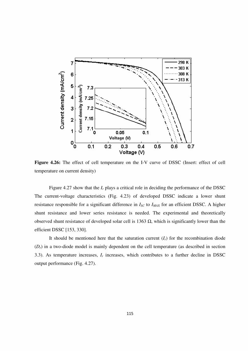
115
Figure 4.26: The effect of cell temperature on the I-V curve of DSSC (Insert: effect of cell
temperature on current density)
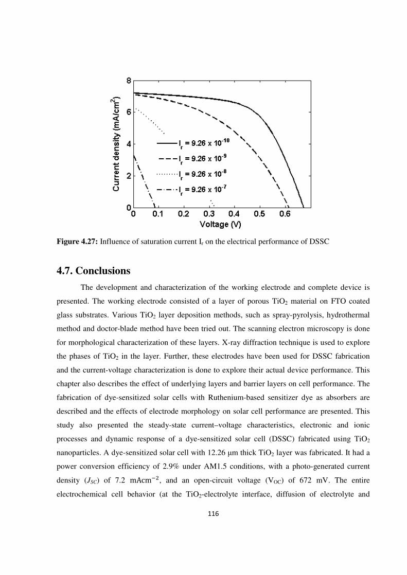
Figure 4.27 show that the Ir plays a critical role in deciding the performance of the DSSC
The current-voltage characteristics (Fig. 4.23) of developed DSSC indicate a lower shunt
resistance responsible for a significant difference in ISC to IMAX for an efficient DSSC. A higher
shunt resistance and lower series resistance is needed. The experimental and theoretically
observed shunt resistance of developed solar cell is 1363 Ω, which is significantly lower than the
efficient DSSC [153, 330].
It should be mentioned here that the saturation current (Ir) for the recombination diode
(Dr) in a two-diode model is mainly dependent on the cell temperature (as described in section
3.3). As temperature increases, Ir increases, which contributes to a further decline in DSSC
output performance (Fig. 4.27).
116
Figure 4.27: Influence of saturation current Ir on the electrical performance of DSSC
4.7. Conclusions
The development and characterization of the working electrode and complete device is
presented. The working electrode consisted of a layer of porous TiO2 material on FTO coated
glass substrates. Various TiO2 layer deposition methods, such as spray-pyrolysis, hydrothermal
method and doctor-blade method have been tried out. The scanning electron microscopy is done
for morphological characterization of these layers. X-ray diffraction technique is used to explore
the phases of TiO2 in the layer. Further, these electrodes have been used for DSSC fabrication
and the current-voltage characterization is done to explore their actual device performance. This
chapter also describes the effect of underlying layers and barrier layers on cell performance. The
fabrication of dye-sensitized solar cells with Ruthenium-based sensitizer dye as absorbers are
described and the effects of electrode morphology on solar cell performance are presented. This
study also presented the steady-state current–voltage characteristics, electronic and ionic
processes and dynamic response of a dye-sensitized solar cell (DSSC) fabricated using TiO2
nanoparticles. A dye-sensitized solar cell with 12.26 µm thick TiO2 layer was fabricated. It had a
power conversion efficiency of 2.9% under AM1.5 conditions, with a photo-generated current
density (JSC) of 7.2 mAcmn, and an open-circuit voltage (VOC) of 672 mV. The entire
electrochemical cell behavior (at the TiO2-electrolyte interface, diffusion of electrolyte and

117
charge transfer at counter electrode) was mathematically modeled using an AC electrical
equivalent circuit. The effect of temperature and illumination on the steady state and dynamic
parameters of DSSCs was also studied. A positive temperature coefficient of dynamic resistance
is observed. The dynamic resistance of DSSC decreases from 440.7 Ω to 78.6 Ω with increase in
illumination level from 20 mWcmn to 100 mWcmn. It is found that the saturation current of
the rectifying diode and the saturation current of the recombination diode are responsible for the
recombination losses and have major influence on the overall conversion efficiency.