Embed Size (px)
Citation preview
SIMULATION OF SEMICONDUCTOR LITHOGRAPHY AND TOPOGRAPHY - ARN 95
CHAPTER 4 Characterization of Deposition and Etching
The physical mechanisms in deposition and etching give rise to key trade-offs which are important in characterizing processes and equipment modeling for deposition, etching and planarization unit processes. The development of a give unit process is important in its own right. However, it is even more important on a global scale to understanding of the flexibility within a process and the manner in which it interacts with other unit processes for creating process flow sequences for integration. Untested pattern level to pattern level interactions can result in unanticipated gotchas when a process is moved into production. Having sufficient understanding to avoid them gives important leverage. New processes for deposition and etching are constantly being developed and characterizing and model-ing these processes is a hot topic in TCAD research. A number of major simulator exten-sions for these advanced processes will be considered.
4.1 Designing Deposition Processes
Test structures such as long lines are often used to characterize deposition systems. The long lines are easy to cross sections and SEM. It is important to examine lines with the two principal orientations parallel and perpendicular to the incidence plane formed by the wafer normal and the system axis. The geometry of an evaporation system is shown in Figure 4.1. An undercut resist profile was used to test this system and the results for a 1 μm line and space pattern are shown in Figure 4.2.The parameters shown on the simulated profile describe the system geometry. When the lines on the wafer are perpendicular to the incidence plane the sidewall is not as effectively coated when the wafer is at the top of the dome. This occurs when the wafer is fastened to the rotating dome. If the apparatus is modified such that the wafer can spin independently of the dome this orientation effect is eliminated
The geometrical nature of deposition provides important leverage in designing metal lift-off processes. The simulation in Figure 4.3 shows the profile time-evolution during evapo-

Characterization of Deposition and Etching
96 SIMULATION OF SEMICONDUCTOR LITHOGRAPHY AND TOPOGRAPHY - ARN 3/3/06
ration and the final SiO2 coated profile (once the resist and metal on top is lifted). Deposi-tion nearly vertical to the wafer is required. This is difficult to achieve along with uniformity of thickness across a load of wafers. The thickness of deposition can be adjusted by moving wafers closer to the source on the edges. As a result the dome is not
FIGURE 4.1 Evaporator geometry which is designed to produce good step coverage [rzz.arn.iee].
FIGURE 4.2 SEM of aluminum deposition onto the test structure for the symmetric and asymmetrical cases and comparison with modeling and simulation [rzz.arn.ieee].

Designing Plasma Etching Processes
3/3/06 SIMULATION OF SEMICONDUCTOR LITHOGRAPHY AND TOPOGRAPHY - ARN 97
spherical and wafers may receive flux from off-axis. Of particular concern is the small foot of metal which occurs when the angle is not exactly vertical.The SEMs in Figure 4.4 show this foot in detail.
4.2 Designing Plasma Etching Processes
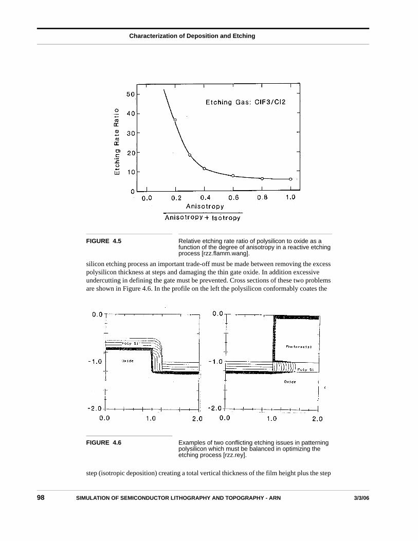
In reactive ion etching the relative etch rate of the unmasked and masked regions is a func-tion of the operating parameters which gives the technologists choices in designing the unit process. For example, Figure 4.5 shows that this etching rate ratio drops rapidly as the degree of anisotropy increases. This is due to the fact that in increasing the degree of anisotropy the role of less selective ion bombardment is increased. In designing the poly-
FIGURE 4.3 Lift-off process showing initial profile, time-evolution of aluminum evaporation, profile after lifting and interlayer dielectric deposition [zz.winm].
FIGURE 4.4 SEMs of the lift-off profiles prior to and after lifting. Not the small foot on the edge of the aluminum profile [rzz.winm].
Characterization of Deposition and Etching
98 SIMULATION OF SEMICONDUCTOR LITHOGRAPHY AND TOPOGRAPHY - ARN 3/3/06
silicon etching process an important trade-off must be made between removing the excess polysilicon thickness at steps and damaging the thin gate oxide. In addition excessive undercutting in defining the gate must be prevented. Cross sections of these two problems are shown in Figure 4.6. In the profile on the left the polysilicon conformably coates the
step (isotropic deposition) creating a total vertical thickness of the film height plus the step
FIGURE 4.5 Relative etching rate ratio of polysilicon to oxide as a function of the degree of anisotropy in a reactive etching process [rzz.flamm.wang].
FIGURE 4.6 Examples of two conflicting etching issues in patterning polysilicon which must be balanced in optimizing the etching process [rzz.rey].

Designing Plasma Etching Processes
3/3/06 SIMULATION OF SEMICONDUCTOR LITHOGRAPHY AND TOPOGRAPHY - ARN 99
height. It is necessary to remove this ‘stringer’ completely as otherwise it will act as a short circuit between polysilicon features in front of and in back of this cross sectional cut. The additional height could be removed by overetching. However, at the bottom of the trench lies the critically important and very thin gate oxide. To limit the loss of thin oxide high selectivity might be utilized by operating at a low degree of anisotropy. The low selectivity, however, causes undercutting in the etching of the gate structure shown on the right hand side of Figure 4.6. This linewidth loss must be traded-off against the amount of gate oxide on the source/drain area which is etched. Typical data for linewidth loss and oxide thickness loss as a function of the degree of anisotropy is shown in Figure 4.7.
When the polysilicon is silicided to reduce the sheet resistance the etching process must be carefully be modified to preserve a vertical sidewall through both the silicided and regular polysilicon beneath it [rzz.siemens.tasi]. As shown in Figure 4.8 the two layers of the gate material may have differing etch rates which produces a stepped edge of the gate structure. In characterizing such a process parameters such as the gas mixture, pressure and power are typically examined. A robust process must be found which is insensitive to manufac-turing issues such as uniformity (location on the wafer) and loading. The loading effect here occurs because the relative amount of TaSi2 and polysilicon being etched changes abruptly each time the etch front reaches another interface between these materials. Ini-tially TaSi2 loads the system, then polysilicon and in overetching there is no loading. The loading is roughly proportional to the area of a particular material being etched. It sud-denly drops to almost zero when the etch front reaches an interface and only the sidewall area remains.
FIGURE 4.7 Linewidth loss and gate oxide etched as a function of the degree of anisotropy in etching polysilicon [rzz.rey].

Characterization of Deposition and Etching
100 SIMULATION OF SEMICONDUCTOR LITHOGRAPHY AND TOPOGRAPHY - ARN 3/3/06
4.3 Planarization
Many of the processing problems such as step coverage are aggravated by the topographi-cal features which tend to be enhanced with each step inn the process. This topography propagation effect was evident from the lift-off process and subsequent SiO2 deposition in Figure 4.3. One simple approach for reducing the topography effects is to use the phos-phosilicate glass (PSG) reflow shown in Figure 4.9. The PSG process consists of first
sputter depositing oxide which produces the initial shape. In a thermal treatment with phosphorous (and sometimes boron containing gas) the upper layer of this oxide is con-verted to a glassy layer which will reflow at temperatures around 950oC. This temperature
FIGURE 4.8 Etching of a TaSi2 gate material and the stepped profile which results from dissimilarity in the etch rates of the too materials.
FIGURE 4.9 PSG process showing as deposited profile and its evolution in reflow and an SEM of the final shape [rzz.sutjarda].

Planarization
3/3/06 SIMULATION OF SEMICONDUCTOR LITHOGRAPHY AND TOPOGRAPHY - ARN 101
is sufficiently low that the dopants in the shallow source/drain regions due not tend to increase the junction depth.
A method of reducing the accumulating topography through planarized sputter deposited SiO2 was reported by Ting et al. [rzz.ting.in.arn.seg]. The process consists of using a sub-strate bias voltage or a separate RF-power driven substrate to adjust the resputtering of the substrate during sputtering of SiO2. The resputtering improves the quality of the SiO2 for passivation and eliminates the ‘rat hole’ problem.
Without substrate bias, the deposition process appears, to first order, to have a deposition rate independent of angle. This is evident from the almost equal lateral and vertical cover-age of features seen in SEM’s and can be modeled by a constant deposition rate versus angle. Biasing the substrate tends to increase the bombardment and hence, induce reduce resputtering of the deposited material. To first order, the ion bombardment resputtering is analogous to ion milling and can be modeled by the etch rate dependence on angle shown in Figure 4.10 . The simultaneous etching and deposition in this process subtract from
each other result in a net deposition for surfaces with angles less than 30o and etching of surfaces with angles from 30o to nearly vertical.
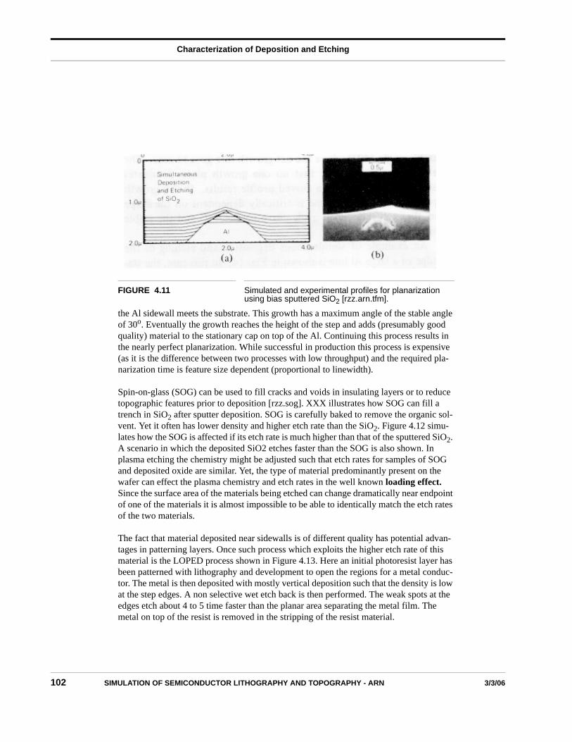
An example of an experimental and simulated profiles are shown in Figure 4.11. The sim-ulation clearly shows how the profile evolves with time. On top of the Al and on the sub-strate the SiO2 slowly deposits. The SiO2 on top of the Al attempts to form a square corner. However, multiple faceting exists there. If the angle is ever steeper than 30o etch-ing occurs and material is removed. If the angle is ever larger than 30o material is depos-ited. Thus a cap of deposited material with the stable 30o angle builds up and comes to a stop. Meanwhile growth planes at shallow angles are generated from the point at which
FIGURE 4.10 Etch rate versus angle for resputtering and deposition rate versus angle for bias sputtering planarization [rzz.arn.tfd].
Characterization of Deposition and Etching
102 SIMULATION OF SEMICONDUCTOR LITHOGRAPHY AND TOPOGRAPHY - ARN 3/3/06
the Al sidewall meets the substrate. This growth has a maximum angle of the stable angle of 30o. Eventually the growth reaches the height of the step and adds (presumably good quality) material to the stationary cap on top of the Al. Continuing this process results in the nearly perfect planarization. While successful in production this process is expensive (as it is the difference between two processes with low throughput) and the required pla-narization time is feature size dependent (proportional to linewidth).
Spin-on-glass (SOG) can be used to fill cracks and voids in insulating layers or to reduce topographic features prior to deposition [rzz.sog]. XXX illustrates how SOG can fill a trench in SiO2 after sputter deposition. SOG is carefully baked to remove the organic sol-vent. Yet it often has lower density and higher etch rate than the SiO2. Figure 4.12 simu-lates how the SOG is affected if its etch rate is much higher than that of the sputtered SiO2. A scenario in which the deposited SiO2 etches faster than the SOG is also shown. In plasma etching the chemistry might be adjusted such that etch rates for samples of SOG and deposited oxide are similar. Yet, the type of material predominantly present on the wafer can effect the plasma chemistry and etch rates in the well known loading effect. Since the surface area of the materials being etched can change dramatically near endpoint of one of the materials it is almost impossible to be able to identically match the etch rates of the two materials.
The fact that material deposited near sidewalls is of different quality has potential advan-tages in patterning layers. Once such process which exploits the higher etch rate of this material is the LOPED process shown in Figure 4.13. Here an initial photoresist layer has been patterned with lithography and development to open the regions for a metal conduc-tor. The metal is then deposited with mostly vertical deposition such that the density is low at the step edges. A non selective wet etch back is then performed. The weak spots at the edges etch about 4 to 5 time faster than the planar area separating the metal film. The metal on top of the resist is removed in the stripping of the resist material.
FIGURE 4.11 Simulated and experimental profiles for planarization using bias sputtered SiO2 [rzz.arn.tfm].

Planarization
3/3/06 SIMULATION OF SEMICONDUCTOR LITHOGRAPHY AND TOPOGRAPHY - ARN 103
FIGURE 4.12 Spin-on-glass (a) as deposited to fill a trench and the resulting topography in etch back (b) when the SOG etches much more rapidly than the SiO2 or (c) when the SiO2 etches slightly faster than the SOG [rzz.lyons].
FIGURE 4.13 LOPED process as simulated by SAMPLE [rzz.lyons.kodak].
(c)
(b)(a)

Characterization of Deposition and Etching
104 SIMULATION OF SEMICONDUCTOR LITHOGRAPHY AND TOPOGRAPHY - ARN 3/3/06
4.4 Integration Versus Unit Process Perfection
If the conditions and circumstances that are relevant to using a unit process step in a pro-cess flow sequence are well defined then perfection of the unit process is very helpful. In many situations, however, it may be more important to devote some of the limited time and resources to understanding the range of what is possible in a unit process and to exam-ine how trade-offs between process steps can improve the overall process flow. This is particularly true for back-of-the-line processes involving the etching and deposition pro-cesses discussed in this chapter.
A basic example of patterning and metalizing contact holes is shown in Figure 4.14 [rxx.sakai.con]. Here a three step process flow of patterning the resist, transferring the pat-
tern to the SiO2, and metalization is shown. The left set of cross sections shows a contact etch with a very vertical sidewall. Obtaining perfectly vertical sidewalls is a noble goal and no simple task. Yet in looking a the subsequent deposition of metal it is clear that self shadowing and perhaps mutual shadowing of vertical walls results in poor sidewall cover-age. The set of cross sections on the right show much better sidewall coverage owing to the taper of the oxide profile. The detailed shape of the taper is not essential. An adequate taper could be produced by controlled undercutting in the oxide etching unit process, by tapering the resist profile in lithography, or combinations of both. From the process inte-gration point of view it is clear that there are many choices and the options increase with
FIGURE 4.14 Improved design for a contact filling process through tapering of sidewalls [rzz.sakai.con]. (Test structures were trenches.)

Integration Versus Unit Process Perfection
3/3/06 SIMULATION OF SEMICONDUCTOR LITHOGRAPHY AND TOPOGRAPHY - ARN 105
the knowledge of the breadth of what is possible in each unit process. The process integra-tor has many choices and thus freedom to select an approach which gives the best overall manufacturability. As usual there is a consequence for every improvement and in this case the sidewall coverage comes at the expense of the greater lateral dimension of the contact which will likely affect spacing design rules and hence overall packing density.
The buried contact structure shown in Figure 4.15 is another classical example of where process integration is an issue. The buried contact is formed by adding an extra mask to
open the thin oxide such that the polysilicon can make direct contact with the substrate. The out diffusion of the dopant from the polysilicon makes the substrate conducting underneath the polysilicon and this n+ region merges with the implant through the open-ing as well as the adjacent implant through the gate oxide in the source/drain region. A problem in generating this structure is that the silicon substrate in the buried contact win-dow which is not protected by the polysilicon inadvertently suffers a certain amount of etching. A trench as deep as half of the polysilicon thickness can be result and this makes it difficult for the out diffusion from the polysilicon to link up with low resistance to the implant in the bottom of the trench.
The dominant factor contributing to the depth of the trench is the wall angle on the isola-tion. Since the poysilicon covering the isolation at angle ΘISO must be etched a vertical distance 1/cosΘISO an over etch of (1/cosΘIOS -1) is needed. For a 45o isolation angle this is a 41% overetch and assuming silicon etches at the same rate as polysilicon a trench depth dTRENCH = 0.41 tPOLY results. Nonuniformity factors for the polysilicon thickness, its etch rate uniformity and the uniformity of the plasma etching can easily increase the trench depth to well over 50% of the polysilicon thickness. To compensate for a deep trench the Dt product for the out diffusion of the polysilicon can be increased but this affects increases the encroachment of the source and drain under the gate. So for the bur-
FIGURE 4.15 Buried contact process integration issue of the polysilicon etc. attacking the substrate and creating a height offset which creates difficulty in laterally linking the electrically conducting doped regions for low resistance.
ΘISO
StringerProblem
OveretchCreates Trench
Dopant HasProblem Linking
n+n+n+
n+
Poly
Oxide
GateΔTRENCH
Isolation

Characterization of Deposition and Etching
106 SIMULATION OF SEMICONDUCTOR LITHOGRAPHY AND TOPOGRAPHY - ARN 3/3/06
ied contact there is a trade-off between the oxide isolation angle, polysilicon uniformity in deposition and etching and the thermal cycle to form the device structure.
4.5 Unanticipated Gotchas
The transfer of a design from development to the high volume production facility can be delayed several weeks and idle the production facility when an unanticipated process inte-gration problem arises. The process development team tries to anticipate likely problems through the use of test structures and test circuits. Yet it is nearly impossible to test in advance every possible critical fabrication scenario used in the actual design. Good design rules generally prevent problems and simulation makes it possible to go through every pattern on a mask and qualify its aerial image at the wafer. Where problems arise is usu-ally in wafer topography from one process step influencing the pattern transfer of a subse-quent step. Unfortunately processes like resist spinning and plasma etching have interaction distances over tens to hundreds of adjacent features which makes the number of combinations to be considered beyond the scope traditional process characterization.
An effect as simple as the proximity of nearby topography on the resulting thickness of resist after spinning known to shut a production line down for as much a six weeks. An simplified illustration is shown in Figure 4.16. Here two lines on the metal 2 mask are to
be patterned to produce identical features on the wafer. They are adjacent to a large feature on the metal 1mask which has produced a large raised area on the wafer. The resist in coat-ing the large feature on the wafer slowly makes a transition from trying to attain its nomi-nal spin thickness on top of the large feature to the corresponding thickness for the area of lower height, The feature being patterned by mask 2 locally sees a thicker resist than the feature further from the large feature. The additional resist thickness make it more difficult to successfully pattern the feature adjacent to the large pre-existing feature on the sub-strate. Even if the adjacent line is defined it will likely be of different width than the line further from the pre-existing feature.
FIGURE 4.16 Illustration of linewidth change resulting from the proximity of preexisting features during resist spinning.
Unanticipated Gotchas
3/3/06 SIMULATION OF SEMICONDUCTOR LITHOGRAPHY AND TOPOGRAPHY - ARN 107
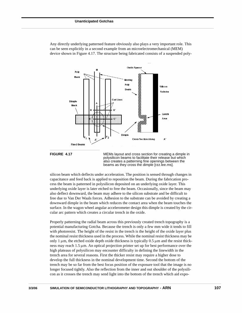
Any directly underlying patterned feature obviously also plays a very important role. This can be seen explicitly in a second example from an microelectromechanical (MEM) device shown in Figure 4.17. The structure being fabricated consists of a suspended poly-
silicon beam which deflects under acceleration. The position is sensed through changes in capacitance and feed back is applied to reposition the beam. During the fabrication pro-cess the beam is patterned in polysilicon deposited on an underlying oxide layer. This underlying oxide layer is later etched to free the beam. Occasionally, since the beam may also deflect downward, the beam may adhere to the silicon substrate and be difficult to free due to Van Der Waals forces. Adhesion to the substrate can be avoided by creating a downward dimple in the beam which reduces the contact area when the beam touches the surface. In the wagon wheel angular accelerometer design this dimple is created by the cir-cular arc pattern which creates a circular trench in the oxide.
Properly patterning the radial beam across this previously created trench topography is a potential manufacturing Gotcha. Because the trench is only a few mm wide it tends to fill with photoresist. The height of the resist in the trench is the height of the oxide layer plus the nominal resist thickness used in the process. While the nominal resist thickness may be only 1 μm, the etched oxide depth oxide thickness is typically 0.5 μm and the resist thick-ness may reach 1.5 μm. An optical projection printer set up for best performance over the high plateaus of polysilicon may encounter difficulty in defining the linewidth in the trench area for several reasons. First the thicker resist may require a higher dose to develop the full thickness in the nominal development time. Second the bottom of the trench may be so far from the best focus position of the exposure tool that the image is no longer focused tightly. Also the reflection from the inner and out shoulder of the polysili-con as it crosses the trench may send light into the bottom of the trench which aid expo-
FIGURE 4.17 MEMs layout and cross section for creating a dimple in polysilicon beams to facilitate their release but which also creates a patterning fine openings between the beams as they cross the dimple [rzz.lee.ms].

Characterization of Deposition and Etching
108 SIMULATION OF SEMICONDUCTOR LITHOGRAPHY AND TOPOGRAPHY - ARN 3/3/06
sure or reduce exposure through constructive or destructive interference with the direct light. From any of these causes a thin residue of unexposed resist can remain in the trench. During the subsequent plasma etch step this residue erodes slowly and leaves insufficient time to etch completely etch the polysilicon film at the bottom of the trench to separate the beams as shown in Figure 4.18
Within a process flow there are usually multiple choices for possible minor changes at a number of process steps which could be utilized to fix the Gotcha. Solutions might be as simple as increasing the resist exposure dose or development time slightly. The focus of the exposure tool might be shifted downward slightly. The resist descum process could be increased. The resist etch process time could be increased or the etch selectivity could be reduced initially to rapidly erode the residue., A possible layout related fix is to reduce the width of the trench such that the polysilicon completely fills the trench and the resist thickness is near its nominal value. This, however, means that in etching the polysilicon the overetch would have to be sufficient to etch polysilicon of a thickness equal to the oxide height plus the nominal polysilicon height. Since there are so many options, it is important to have an understanding of the flexibility possible in each process step as pos-sible options and the interdependencies between process steps which affect exercising the options.
4.6 Characterizing Advanced Processes
The characterization of etching and deposition has revealed evidence of many factors which potentially influence the resultant device topography. Figure 4.19 lists a number of these for dry etching compiled from the literature [rzz.sch.phd]. Both ions and reactive neutrals arrive at the mask opening. The ions have an angular dependent sputtering rate and may reflect off of the sidewall. The arriving species have surface reaction coefficients, may diffuse along the arc length of the surface, and may even bounce due to a sticking coefficient less than unity. Polymer deposition from the plasma and resputtered material may passivated the surface. There is even some evidence of the charging of the profile affecting the arrival of electrons from the plasma.
FIGURE 4.18 Cross section of MEMs dimple process [rzz.lee.ms].

Characterizing Advanced Processes
3/3/06 SIMULATION OF SEMICONDUCTOR LITHOGRAPHY AND TOPOGRAPHY - ARN 109
The SAMPLE-3D process simulator was designed to support both the calculation of arriv-ing species, surface migration and reactions, reflection, etching of redeposited inhomoge-neous materials, as well as surface advance in 3D [rzz.sch.PhD]. Figure 4.20 shows 3D effects in defining features in lithography and deposition. On the left a negative DUV pho-
toresist SBR-248 has been patterned by exposure and development. The resulting profile is then reactive ion etched (RIE) into the substrate. Note that in the region between the narrow lines less etching takes place due to shadowing of the incident flux in what is known as the RIE-lag effect. In deposition on the right the shadowing and tilt of the step
FIGURE 4.19 Physical factors of interest in characterizing dry etching [rzz.sch.phd].
FIGURE 4.20 Typical topographies from defining features in 3D as simulated by SAMPLE-3D [rzz.sch.vlsi].
Characterization of Deposition and Etching
110 SIMULATION OF SEMICONDUCTOR LITHOGRAPHY AND TOPOGRAPHY - ARN 3/3/06
reduces the metal thickness on the sidewall. This effect is of course much more pro-nounced at the inside corner of the trench.
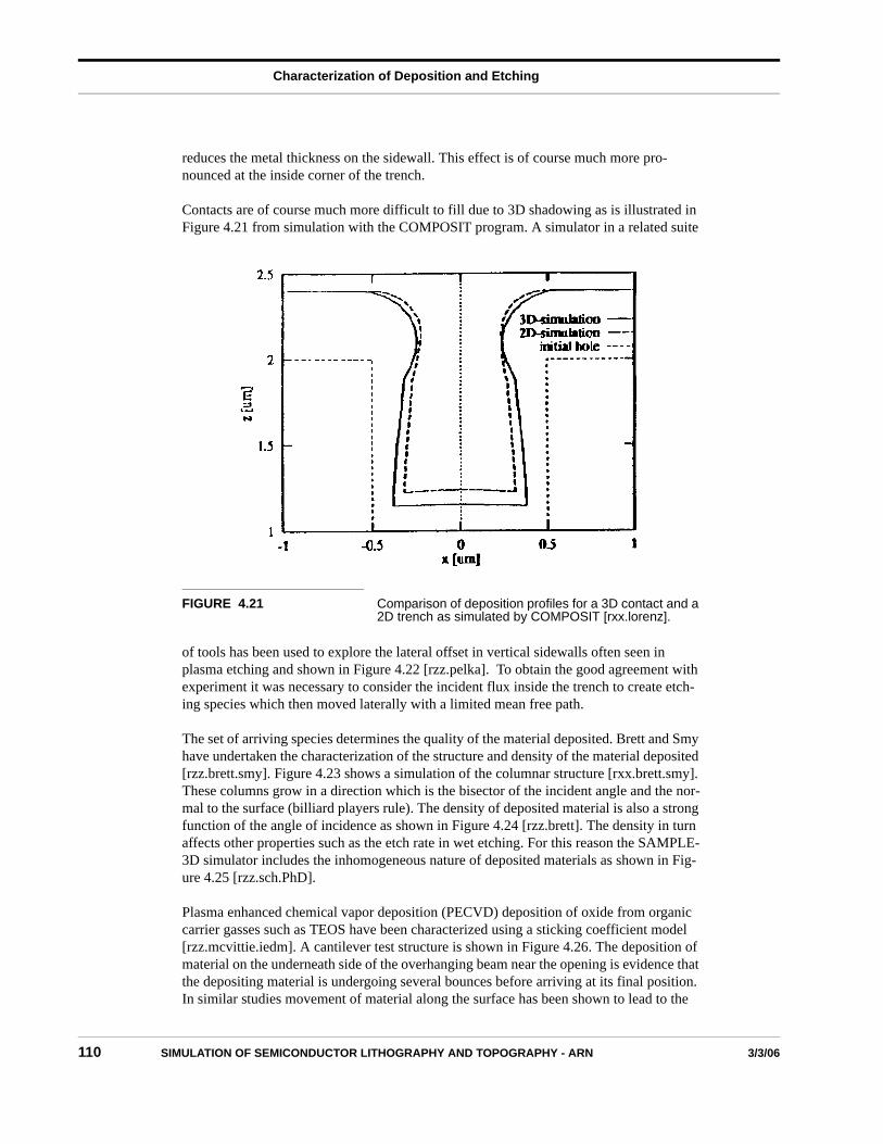
Contacts are of course much more difficult to fill due to 3D shadowing as is illustrated in Figure 4.21 from simulation with the COMPOSIT program. A simulator in a related suite
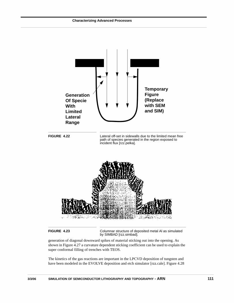
of tools has been used to explore the lateral offset in vertical sidewalls often seen in plasma etching and shown in Figure 4.22 [rzz.pelka]. To obtain the good agreement with experiment it was necessary to consider the incident flux inside the trench to create etch-ing species which then moved laterally with a limited mean free path.
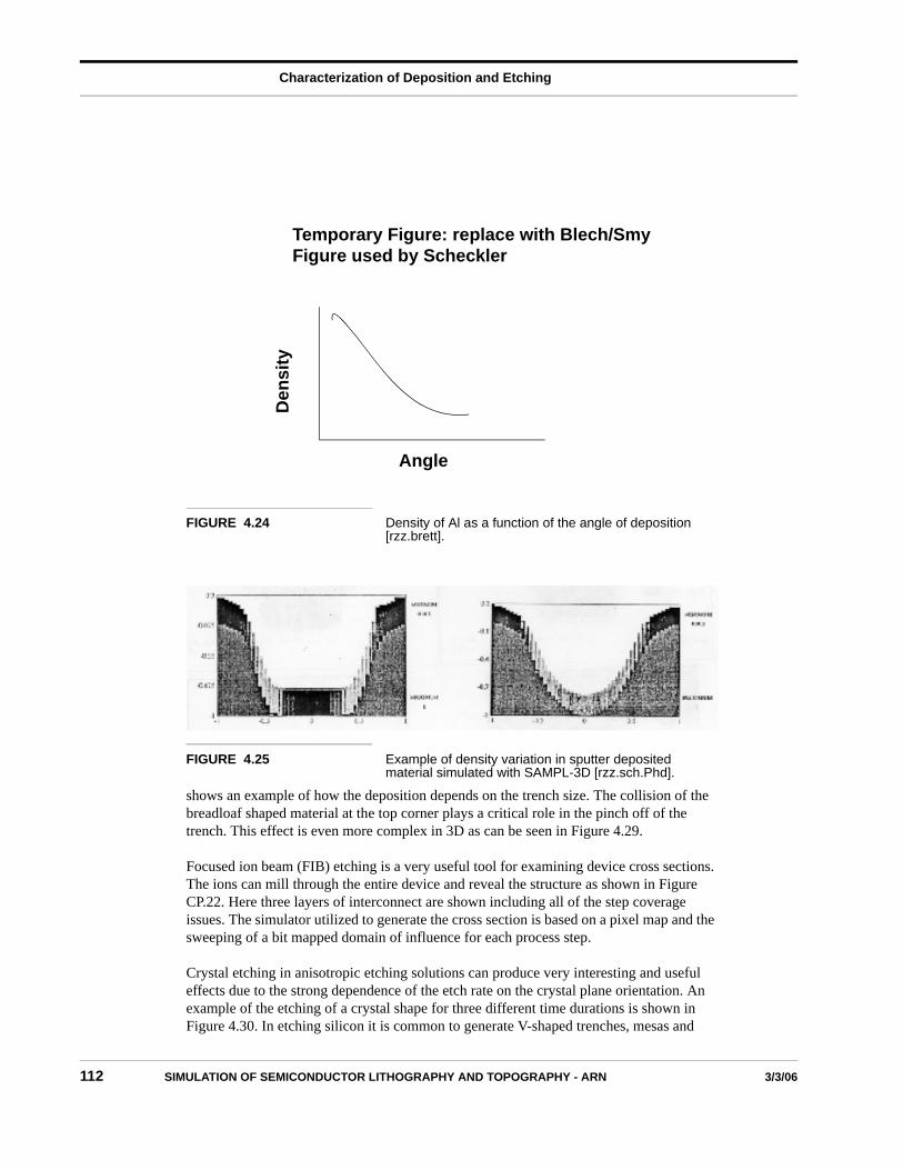
The set of arriving species determines the quality of the material deposited. Brett and Smy have undertaken the characterization of the structure and density of the material deposited [rzz.brett.smy]. Figure 4.23 shows a simulation of the columnar structure [rxx.brett.smy]. These columns grow in a direction which is the bisector of the incident angle and the nor-mal to the surface (billiard players rule). The density of deposited material is also a strong function of the angle of incidence as shown in Figure 4.24 [rzz.brett]. The density in turn affects other properties such as the etch rate in wet etching. For this reason the SAMPLE-3D simulator includes the inhomogeneous nature of deposited materials as shown in Fig-ure 4.25 [rzz.sch.PhD].
Plasma enhanced chemical vapor deposition (PECVD) deposition of oxide from organic carrier gasses such as TEOS have been characterized using a sticking coefficient model [rzz.mcvittie.iedm]. A cantilever test structure is shown in Figure 4.26. The deposition of material on the underneath side of the overhanging beam near the opening is evidence that the depositing material is undergoing several bounces before arriving at its final position. In similar studies movement of material along the surface has been shown to lead to the
FIGURE 4.21 Comparison of deposition profiles for a 3D contact and a 2D trench as simulated by COMPOSIT [rxx.lorenz].
Characterizing Advanced Processes
3/3/06 SIMULATION OF SEMICONDUCTOR LITHOGRAPHY AND TOPOGRAPHY - ARN 111
generation of diagonal downward spikes of material sticking out into the opening. As shown in Figure 4.27 a curvature dependent sticking coefficient can be used to explain the super conformal filling of trenches with TEOS.
The kinetics of the gas reactions are important in the LPCVD deposition of tungsten and have been modeled in the EVOLVE deposition and etch simulator [rzz.cale]. Figure 4.28
FIGURE 4.22 Lateral off-set in sidewalls due to the limited mean free path of species generated in the region exposed to incident flux [rzz.pelka].
FIGURE 4.23 Columnar structure of deposited metal Al as simulated by SIMBAD [rzz.simbad].
GenerationOf SpecieWithLimitedLateralRange
TemporaryFigure(Replace with SEMand SIM)
Characterization of Deposition and Etching
112 SIMULATION OF SEMICONDUCTOR LITHOGRAPHY AND TOPOGRAPHY - ARN 3/3/06
shows an example of how the deposition depends on the trench size. The collision of the breadloaf shaped material at the top corner plays a critical role in the pinch off of the trench. This effect is even more complex in 3D as can be seen in Figure 4.29.
Focused ion beam (FIB) etching is a very useful tool for examining device cross sections. The ions can mill through the entire device and reveal the structure as shown in Figure CP.22. Here three layers of interconnect are shown including all of the step coverage issues. The simulator utilized to generate the cross section is based on a pixel map and the sweeping of a bit mapped domain of influence for each process step.
Crystal etching in anisotropic etching solutions can produce very interesting and useful effects due to the strong dependence of the etch rate on the crystal plane orientation. An example of the etching of a crystal shape for three different time durations is shown in Figure 4.30. In etching silicon it is common to generate V-shaped trenches, mesas and
FIGURE 4.24 Density of Al as a function of the angle of deposition [rzz.brett].
FIGURE 4.25 Example of density variation in sputter deposited material simulated with SAMPL-3D [rzz.sch.Phd].
Temporary Figure: replace with Blech/SmyFigure used by Scheckler
Angle
Den
sity

Characterizing Advanced Processes
3/3/06 SIMULATION OF SEMICONDUCTOR LITHOGRAPHY AND TOPOGRAPHY - ARN 113
ultra flat surfaces by utilizing the fact that the dense planes etch a hundred times more slowly normal to their dense {1,1,1} planes than other more loosely packed planes. Simu-lation of these etching effects is challenging not only due to the dynamic range of the etch rate but also by the fact that it is often difficult to determine the fast-etching and slow-etching facets which emerge. C.H. Sequin has systematically analyzed the various cases
FIGURE 4.26 Cantilevered test structure for calibrating the sticking coefficient in LPCVD TEOS [rzz.mcvittie.iedm].
FIGURE 4.27 Simulation of TEOS oxide deposition using a curvature dependent sticking coefficient [rzz.mcvittie.iedm].

Characterization of Deposition and Etching
114 SIMULATION OF SEMICONDUCTOR LITHOGRAPHY AND TOPOGRAPHY - ARN 3/3/06
under which faces are generated and disappear and shown that the shape of the surface can be modeled algebraically as a function of time between these events [rzz.sequin.sa]. Based on this analysis, a simulator has been written to follow the 3D etching of crystal structures by stitching together the algebraic solutions over the individual time intervals. In this sim-ulator the user can scan forward or backward in time to investigate effects.
FIGURE 4.28 LPCVD deposition of tungsten as affected by trench size [rzz.cale].
FIGURE 4.29 Corner effect in LPCVD tungsten as simulated by EVOLVE [rzz.cale].

Summary
3/3/06 SIMULATION OF SEMICONDUCTOR LITHOGRAPHY AND TOPOGRAPHY - ARN 115
4.7 Summary
This chapter has illustrated process design, issues in process integration, hidden gotchas in going into production and modeling advance process in deposition and etching. The key ideas are.
• In etching each material has its own etching characteristics and boundaries between materials must be considered and often give rise to faceting.
• Planarization can be accomplished by simultaneous etching and deposition or by spin-on and etch-back of materials.
• It is important to examine how trade-offs between individual process steps can improve the overall process robustness.
• Unanticipated process integration issues often arise in moving from process development to production and are a potential cost effective application for simulation.
• In characterizing advanced processes many physical mechanisms are be con-sidered and are a hot topic in TCAD research.
4.8 References
FIGURE 4.30 Etching of a crystal for three different time durations [rzz.sequin.sa].

Characterization of Deposition and Etching
116 SIMULATION OF SEMICONDUCTOR LITHOGRAPHY AND TOPOGRAPHY - ARN 3/3/06