Embed Size (px)
Citation preview

CHEM 793, 2008 Fall
Chapter 3Basic Crystallography and Electron Diffraction from Crystals
Lecture 13

CHEM 793, 2008 Fall
Announcement
Midterm Exam: Oct. 22, Wednesday, 2:30 – 4:30

CHEM 793, 2008 Fall
Indexing Diffraction Pattern
FCC single crystal Pattern FCC Polycrystalline ring Pattern
000
000
000

CHEM 793, 2008 Fall
Indexing Diffraction Pattern
• Indexing means labeling the diffraction rings and spot with appropriate (hkl)
• Key to determining:
interplanar spacing: d-spacing
lattice parameter, a
crystal orientation
nature of defects
• Cannot do phase identification or defect analysis until diffraction pattern is indexed.
Don’t take any TEM image of a crystal without a corresponding diffraction pattern!
CHEM 793, 2008 Fall
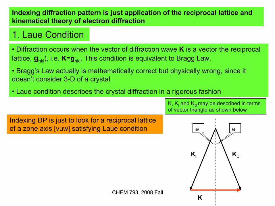
1. Laue Condition• Diffraction occurs when the vector of diffraction wave K is a vector the reciprocal lattice, ghkl), i.e. K=ghkl. This condition is equivalent to Bragg Law.
• Bragg’s Law actually is mathematically correct but physically wrong, since it doesn’t consider 3-D of a crystal
• Laue condition describes the crystal diffraction in a rigorous fashion
KI KD
K
өө
K, KI and KD may be described in terms of vector triangle as shown below
Indexing diffraction pattern is just application of the reciprocal lattice and kinematical theory of electron diffraction
Indexing DP is just to look for a reciprocal lattice of a zone axis [vuw] satisfying Laue condition
CHEM 793, 2008 Fall
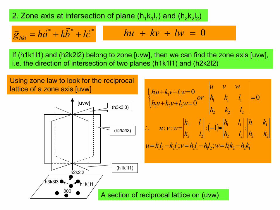
2. Zone axis at intersection of plane (h1k1l1) and (h2k2l2)
[uvw]
(h1k1l1)
(h2k2l2)
(h3k3l3)
• •••••• 000
h1k1l1
h2k2l2
h3k3l3
If (h1k1l1) and (h2k2l2) belong to zone [uvw], then we can find the zone axis [uvw], i.e. the direction of intersection of two planes (h1k1l1) and (h2k2l2)
( )
122121121221
22
11
22
11
22
11
222
111222
111
;;
:1:::
00
0
khkhwlhlhvlklkukhkh
lhlh
lklk
wvu
lkhlkhwvu
orwlvkuhwlvkuh
−=−=−=
•−=∴
=
=++=++
A section of reciprocal lattice on (uvw)
*** clbkahghklrrrv ++= 0=++ lwkvhu
Using zone law to look for the reciprocal lattice of a zone axis [uvw]
CHEM 793, 2008 Fall
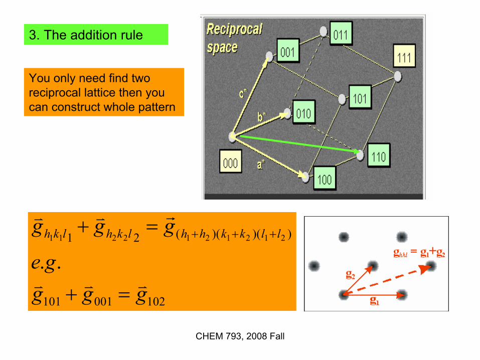
102001101
))()((21
..2121212211
gggge
ggg llkkhhlkhlkh
vvv
rvv
=+
=+ +++
3. The addition rule
You only need find two reciprocal lattice then you can construct whole pattern
CHEM 793, 2008 Fall
21
21
*2
*2
*22
*1
*1
*11
2211
2211
22
11
coslkhlkh
lkhlkh
lkh
lkh
gg
gg
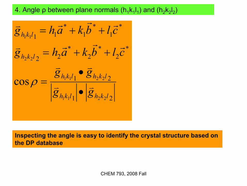
clbkahg
clbkahg
vv
vv
rrrv
rrrv
•
•=
++=
++=
ρ
4. Angle ρ between plane normals (h1k1l1) and (h2k2l2)
Inspecting the angle is easy to identify the crystal structure based on the DP database
CHEM 793, 2008 Fall
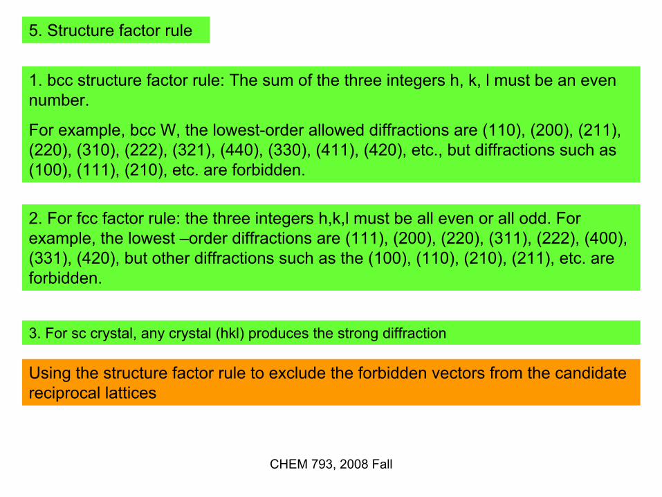
1. bcc structure factor rule: The sum of the three integers h, k, l must be an even number.
For example, bcc W, the lowest-order allowed diffractions are (110), (200), (211), (220), (310), (222), (321), (440), (330), (411), (420), etc., but diffractions such as (100), (111), (210), etc. are forbidden.
5. Structure factor rule
2. For fcc factor rule: the three integers h,k,l must be all even or all odd. For example, the lowest –order diffractions are (111), (200), (220), (311), (222), (400),(331), (420), but other diffractions such as the (100), (110), (210), (211), etc. are forbidden.
3. For sc crystal, any crystal (hkl) produces the strong diffraction
Using the structure factor rule to exclude the forbidden vectors from the candidate reciprocal lattices

CHEM 793, 2008 Fall
Indexing Diffraction Patterns
Three typical DPs:
• A single perfect crystal
• A small number of grains- note that even with three grains the spots begin to form circle
• A large number pf randomly oriented grains-the spots have now merged into rings.
• The amophorousmaterials is also forming the ring pattern (usually only one ring)
CHEM 793, 2008 Fall
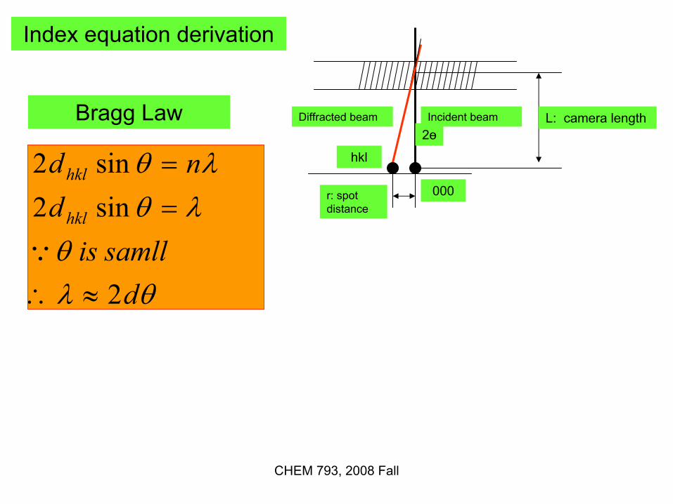
θλθ
λθλθ
dsamllis
dnd
hkl
hkl
2
sin2sin2
≈∴
==
Q
Bragg Law
Index equation derivation
Diffracted beam Incident beam2ө
L: camera length
r: spot distance
hkl
000

CHEM 793, 2008 Fall
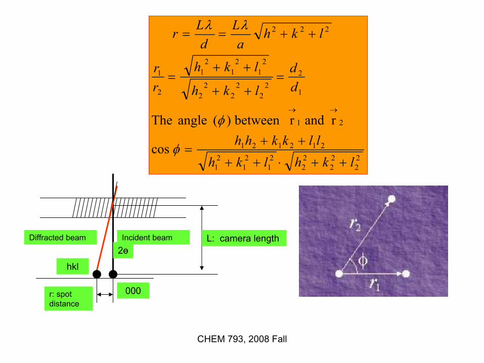
222
222
constant camera called is ,
2
lkhaL
dLr
lkhadand
LLrdordL
rLr
++==∴
++=
=
=∴
=
λλ
λλ
λ
θ
Diffracted beam Incident beam2ө
L: camera length
r: spot distance
hkl
000
CHEM 793, 2008 Fall
22
22
22
21
21
21
212121
21
1
22
22
22
2
21
21
21
2
1
222
cos
r and rbetween )( angle The
lkhlkhllkkhh
dd
lkh
lkhrr
lkhaL
dLr
++⋅++
++=
=++
++=
++==
→→
φ
φ
λλ
Diffracted beam Incident beam2ө
L: camera length
r: spot distance
hkl
000
CHEM 793, 2008 Fall
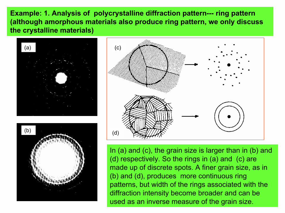
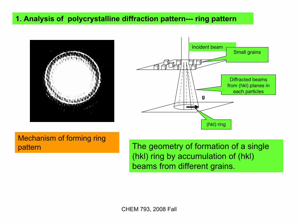
Example: 1. Analysis of polycrystalline diffraction pattern--- ring pattern (although amorphous materials also produce ring pattern, we only discuss the crystalline materials)
(a)
(b)
(c)
(d)
In (a) and (c), the grain size is larger than in (b) and (d) respectively. So the rings in (a) and (c) are made up of discrete spots. A finer grain size, as in (b) and (d), produces more continuous ring patterns, but width of the rings associated with the diffraction intensity become broader and can be used as an inverse measure of the grain size.
CHEM 793, 2008 Fall
1. Analysis of polycrystalline diffraction pattern--- ring pattern
Incident beamSmall grains
Diffracted beams from (hkl) planes in
each particles
(hkl) ring
g
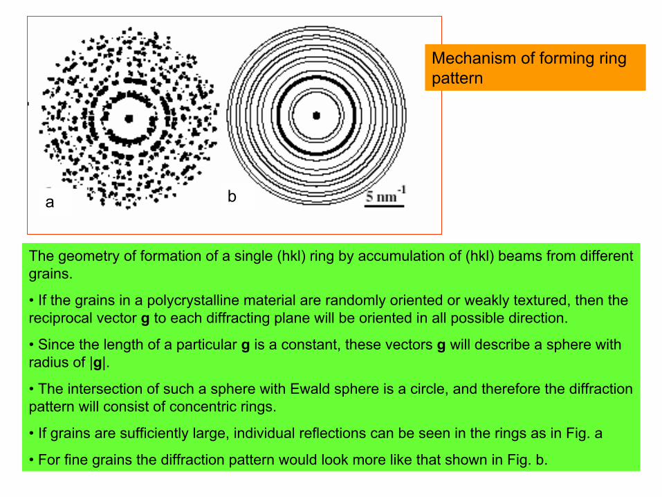
The geometry of formation of a single (hkl) ring by accumulation of (hkl) beams from different grains.
Mechanism of forming ring pattern
CHEM 793, 2008 Fall
The geometry of formation of a single (hkl) ring by accumulation of (hkl) beams from different grains.
• If the grains in a polycrystalline material are randomly oriented or weakly textured, then the reciprocal vector g to each diffracting plane will be oriented in all possible direction.
• Since the length of a particular g is a constant, these vectors g will describe a sphere with radius of |g|.
• The intersection of such a sphere with Ewald sphere is a circle, and therefore the diffraction pattern will consist of concentric rings.
• If grains are sufficiently large, individual reflections can be seen in the rings as in Fig. a
• For fine grains the diffraction pattern would look more like that shown in Fig. b.
a b
Mechanism of forming ring pattern

CHEM 793, 2008 Fall
a
b
c• If texture is present, then one or more rings may be absent, or the intensity in any particular ring may vary along the ring. From an analysis of these intensity distributions, one can, in principal, derive information about the thin foil texture.
• Fig. a shows a texture ring pattern with more intense over a certain angular range, and the corresponding interception of the Ewald sphere with reciprocal lattice
• Fig. b shows a DF image of textured grains, taken from a brighter portion of one of the hklrings, showing an equiaxed structure.
• Fig.c shows the elongated spots or acrs in diffraction pattern, since the specimen is textured about a direction at an angle to the beam.
Planar Ewald sphere
Planar Ewald sphere
CHEM 793, 2008 Fall
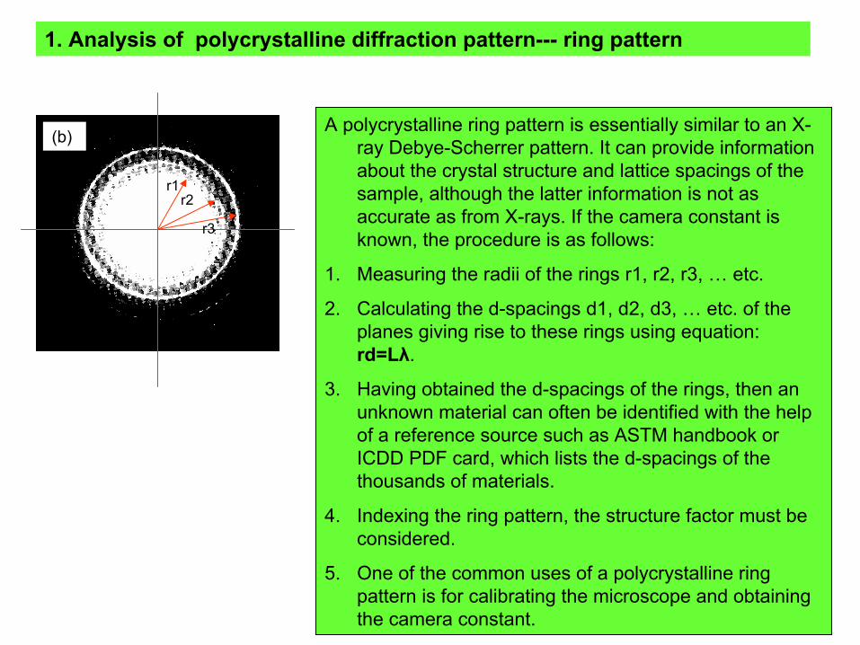
1. Analysis of polycrystalline diffraction pattern--- ring pattern
(b)
r1r2
r3
A polycrystalline ring pattern is essentially similar to an X-ray Debye-Scherrer pattern. It can provide information about the crystal structure and lattice spacings of the sample, although the latter information is not as accurate as from X-rays. If the camera constant is known, the procedure is as follows:
1. Measuring the radii of the rings r1, r2, r3, … etc.
2. Calculating the d-spacings d1, d2, d3, … etc. of the planes giving rise to these rings using equation: rd=Lλ.
3. Having obtained the d-spacings of the rings, then an unknown material can often be identified with the help of a reference source such as ASTM handbook or ICDD PDF card, which lists the d-spacings of the thousands of materials.
4. Indexing the ring pattern, the structure factor must be considered.
5. One of the common uses of a polycrystalline ring pattern is for calibrating the microscope and obtaining the camera constant.
CHEM 793, 2008 Fall
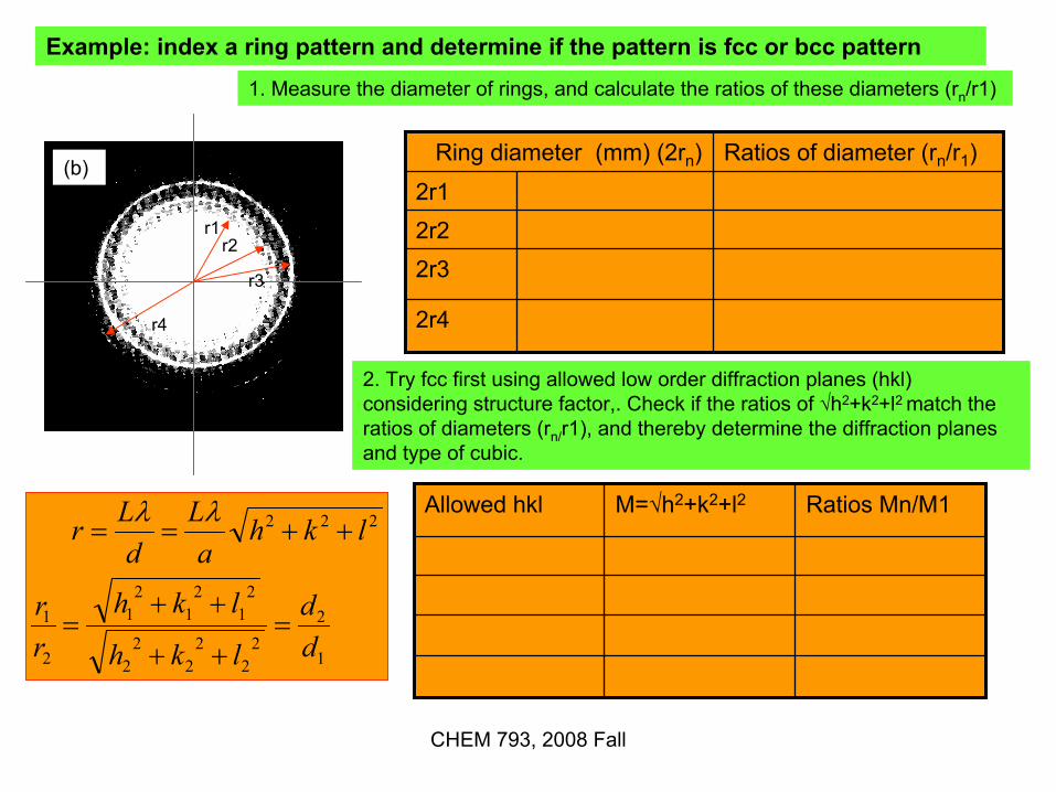
Example: index a ring pattern and determine if the pattern is fcc or bcc pattern
(b)
r1r2
r3
r4
1. Measure the diameter of rings, and calculate the ratios of these diameters (rn/r1)
2r4
2r32r22r1
Ratios of diameter (rn/r1)Ring diameter (mm) (2rn)
1
22
22
22
2
21
21
21
2
1
222
dd
lkh
lkhrr
lkhaL
dLr
=++
++=
++==λλ
2. Try fcc first using allowed low order diffraction planes (hkl) considering structure factor,. Check if the ratios of √h2+k2+l2 match the ratios of diameters (rn/r1), and thereby determine the diffraction planes and type of cubic.
Ratios Mn/M1M=√h2+k2+l2Allowed hkl

CHEM 793, 2008 Fall
Example: index a ring pattern and determine if the pattern is fcc or bcc pattern
r1r2
r3
r4
1
22
22
22
2
21
21
21
2
1
222
dd
lkh
lkhrr
lkhaL
dLr
=++
++=
++==λλ
1.90909090931.52r41.6303030326.92r31.15757575819.12r2
116.52r1Ratios of diameter (rn/r1)Ring diameter (mm) (2rn)
1.9148542163.316624793111.6329931622.8284271252201.1547005382200
11.732050808111Ratios of M (Mn/M1)M=√h^2+k^2+l^2
fcc Allowed hkl
So ratios (rn/r1) match Mn/M1. This ring pattern is fccpattern. Indexing is (111), (200), (220) and (311) from inside to outside
(111)
(200)
(220)
(311)
CHEM 793, 2008 Fall
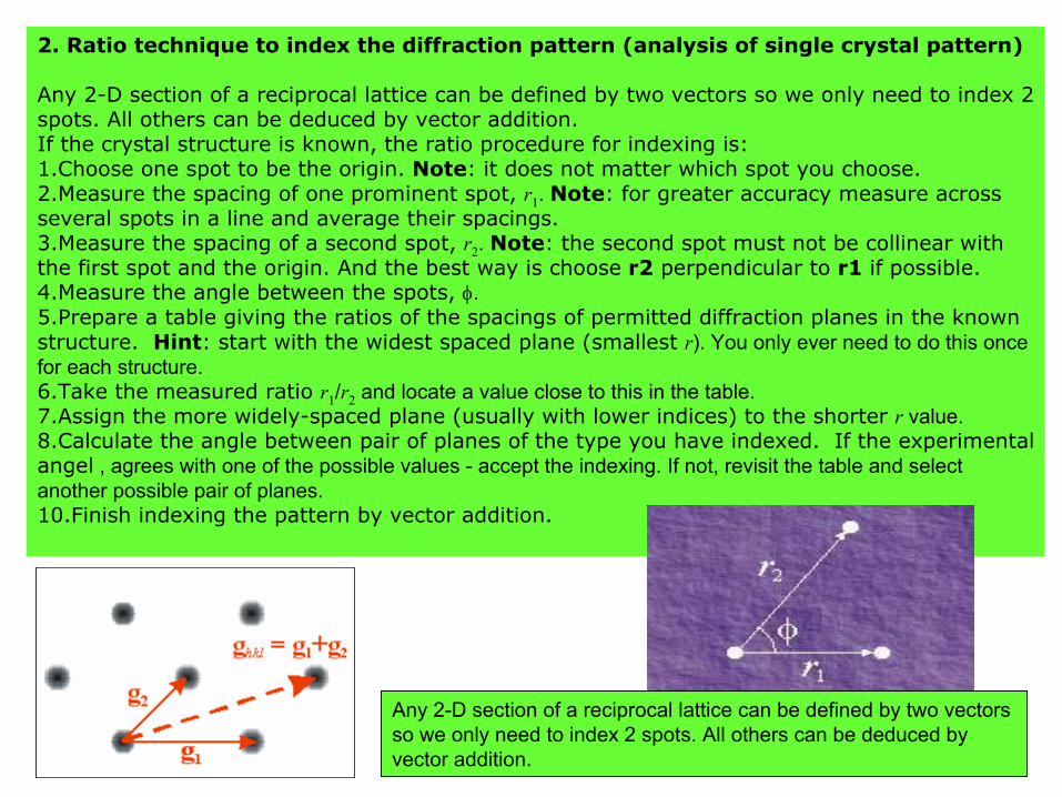
2. Ratio technique to index the diffraction pattern (analysis of single crystal pattern)
Any 2-D section of a reciprocal lattice can be defined by two vectors so we only need to index 2 spots. All others can be deduced by vector addition.If the crystal structure is known, the ratio procedure for indexing is: 1.Choose one spot to be the origin. Note: it does not matter which spot you choose. 2.Measure the spacing of one prominent spot, r1. Note: for greater accuracy measure across several spots in a line and average their spacings. 3.Measure the spacing of a second spot, r2. Note: the second spot must not be collinear with the first spot and the origin. And the best way is choose r2 perpendicular to r1 if possible.4.Measure the angle between the spots, φ. 5.Prepare a table giving the ratios of the spacings of permitted diffraction planes in the known structure. Hint: start with the widest spaced plane (smallest r). You only ever need to do this once for each structure.6.Take the measured ratio r1/r2 and locate a value close to this in the table. 7.Assign the more widely-spaced plane (usually with lower indices) to the shorter r value. 8.Calculate the angle between pair of planes of the type you have indexed. If the experimental angel , agrees with one of the possible values - accept the indexing. If not, revisit the table and select another possible pair of planes. 10.Finish indexing the pattern by vector addition.
Any 2-D section of a reciprocal lattice can be defined by two vectors so we only need to index 2 spots. All others can be deduced by vector addition.
CHEM 793, 2008 Fall
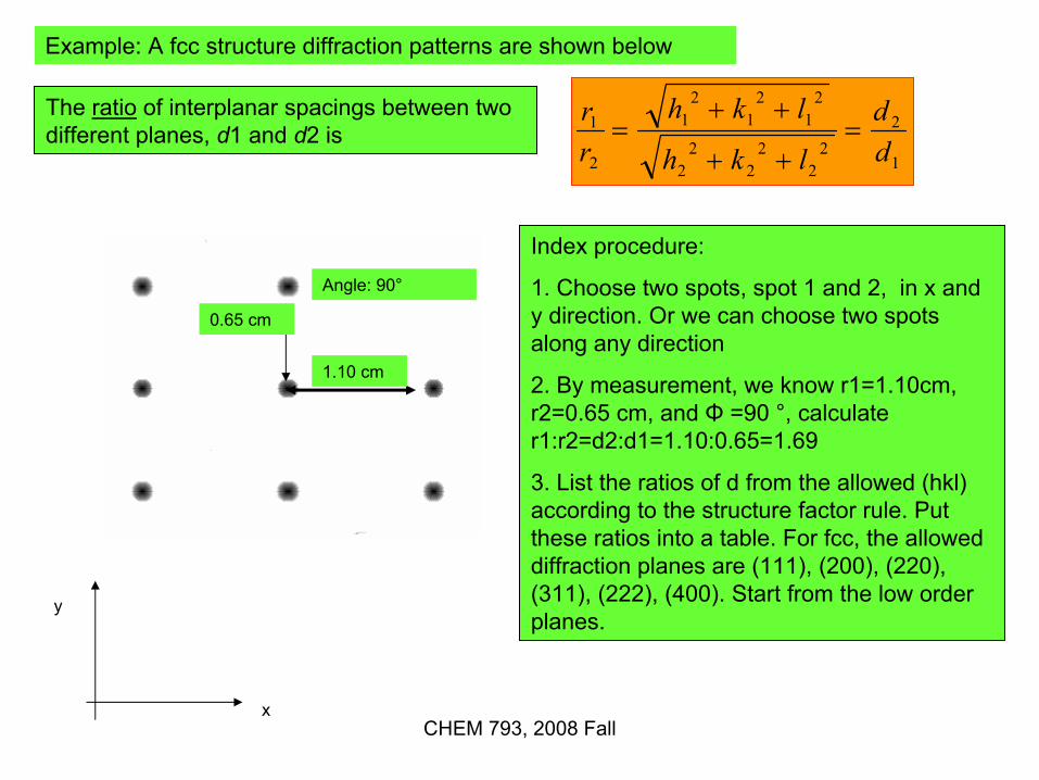
Example: A fcc structure diffraction patterns are shown below
1.10 cm
0.65 cm
Angle: 90°
Index procedure:
1. Choose two spots, spot 1 and 2, in x and y direction. Or we can choose two spots along any direction
2. By measurement, we know r1=1.10cm, r2=0.65 cm, and Φ =90 °, calculate r1:r2=d2:d1=1.10:0.65=1.69
3. List the ratios of d from the allowed (hkl) according to the structure factor rule. Put these ratios into a table. For fcc, the allowed diffraction planes are (111), (200), (220), (311), (222), (400). Start from the low order planes.
x
y
1
22
22
22
2
21
21
21
2
1
dd
lkh
lkhrr
=++
++=
The ratio of interplanar spacings between two different planes, d1 and d2 is
CHEM 793, 2008 Fall
1√16400
1√12222
1√11311
1√8220
1√4200
1√3111
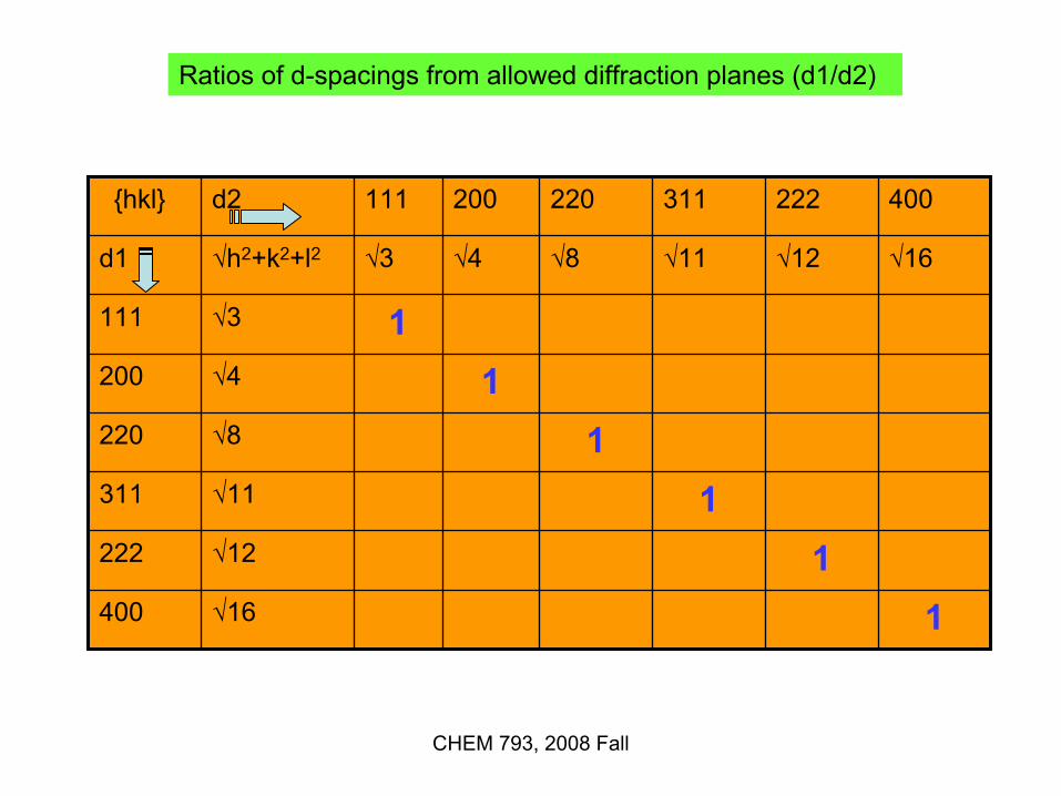
√16√12√11√8√4√3√h2+k2+l2d1
400222311220200111d2{hkl}
Ratios of d-spacings from allowed diffraction planes (d1/d2)
CHEM 793, 2008 Fall
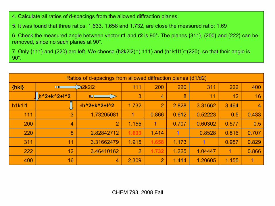
11.1551.206051.41422.309416400
0.86611.044471.2251.73223.4641016212222
0.8290.95711.1731.6581.9153.3166247911311
0.7070.8160.852811.4141.6332.828427128220
0.50.5770.603020.70711.15524200
0.4330.50.522230.6120.86611.732050813111
43.4643.316622.82821.732√h^2+k^2+l^2h1k1l1
161211843h^2+k^2+l^2400222311220200111h2k2l2{hkl}
Ratios of d-spacings from allowed diffraction planes (d1/d2)
4. Calculate all ratios of d-spacings from the allowed diffraction planes.
5. It was found that three ratios, 1.633, 1.658 and 1.732, are close the measured ratio: 1.69
6. Check the measured angle between vector r1 and r2 is 90°. The planes {311}, {200} and {222} can be removed, since no such planes at 90°.
7. Only {111} and {220} are left. We choose (h2k2l2)=(-111) and (h1k1l1)=(220), so that their angle is 90°.
CHEM 793, 2008 Fall
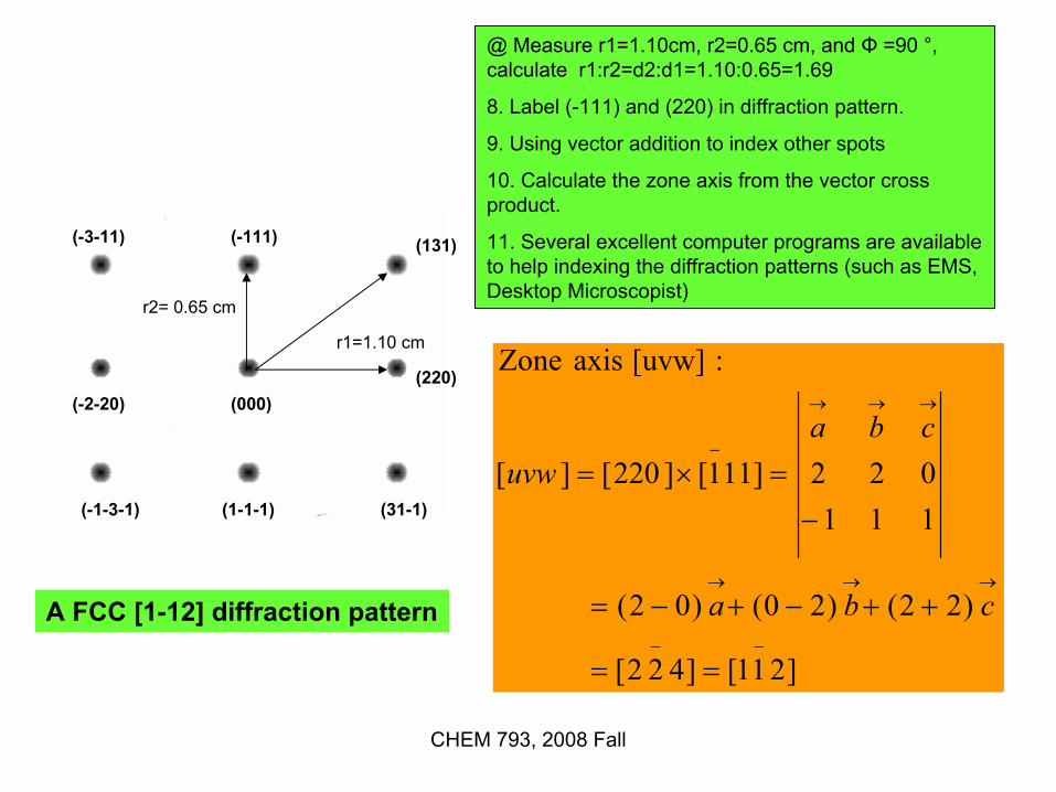
@ Measure r1=1.10cm, r2=0.65 cm, and Φ =90 °, calculate r1:r2=d2:d1=1.10:0.65=1.69
8. Label (-111) and (220) in diffraction pattern.
9. Using vector addition to index other spots
10. Calculate the zone axis from the vector cross product.
11. Several excellent computer programs are available to help indexing the diffraction patterns (such as EMS, Desktop Microscopist)
(-111)
(220)
(131)
r1=1.10 cm
r2= 0.65 cm
(1-1-1)
(000)(-2-20)
(-3-11)
(-1-3-1) (31-1)
]211[]422[
)22()20()02(
111022]111[]220[][
:[uvw] axisZone
−−
→→→
→→→
−
==
++−+−=
−=×=
cba
cbauvw
A FCC [1-12] diffraction pattern

CHEM 793, 2008 Fall
Kinematical Simulation of Aluminum
On-line simulation is available at http://emaps.mrl.uiuc.edu/
CHEM 793, 2008 Fall
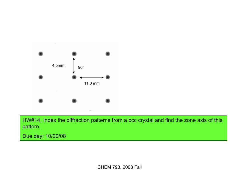
4.5mm
11.0 mm
90°
HW#14, Index the diffraction patterns from a bcc crystal and find the zone axis of this pattern.
Due day: 10/20/08
CHEM 793, 2008 Fall
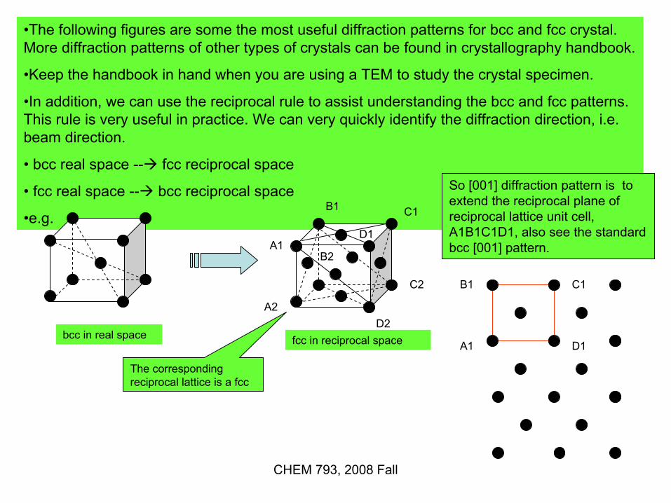
•The following figures are some the most useful diffraction patterns for bcc and fcc crystal. More diffraction patterns of other types of crystals can be found in crystallography handbook.
•Keep the handbook in hand when you are using a TEM to study the crystal specimen.
•In addition, we can use the reciprocal rule to assist understanding the bcc and fcc patterns. This rule is very useful in practice. We can very quickly identify the diffraction direction, i.e. beam direction.
• bcc real space -- fcc reciprocal space
• fcc real space -- bcc reciprocal space
•e.g.
bcc in real space fcc in reciprocal space
A1
C1B1
D1
D2A2
B2
C2
So [001] diffraction pattern is to extend the reciprocal plane of reciprocal lattice unit cell, A1B1C1D1, also see the standard bcc [001] pattern.
A1
B1 C1
D1
The corresponding reciprocal lattice is a fcc
CHEM 793, 2008 Fall
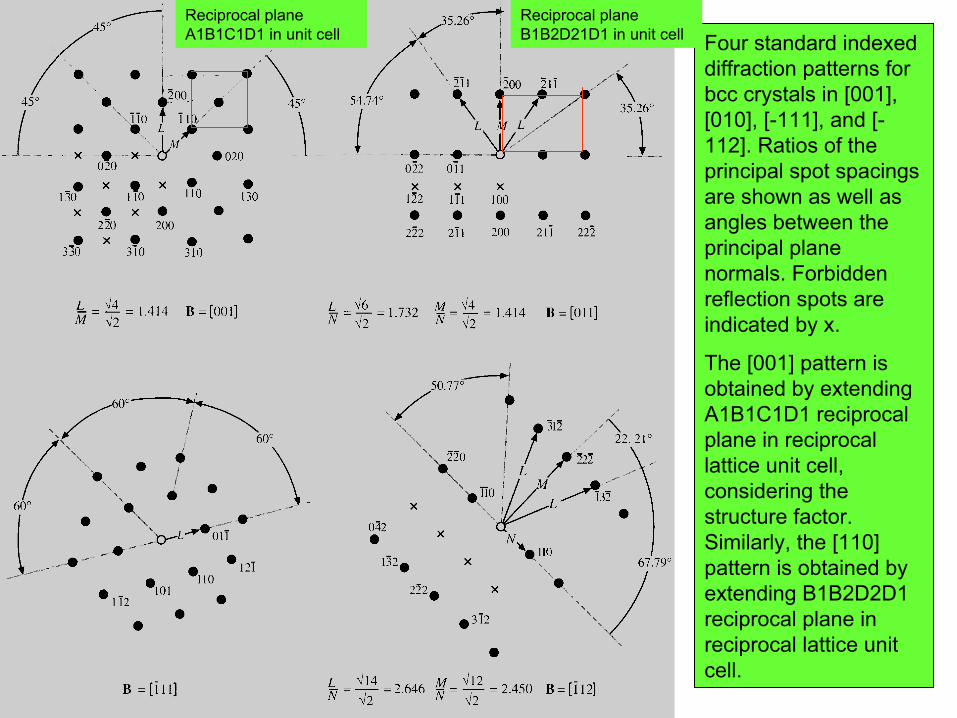
Four standard indexed diffraction patterns for bcc crystals in [001], [010], [-111], and [-112]. Ratios of the principal spot spacingsare shown as well as angles between the principal plane normals. Forbidden reflection spots are indicated by x.
The [001] pattern is obtained by extending A1B1C1D1 reciprocal plane in reciprocal lattice unit cell, considering the structure factor. Similarly, the [110] pattern is obtained by extending B1B2D2D1 reciprocal plane in reciprocal lattice unit cell.
Reciprocal plane A1B1C1D1 in unit cell
Reciprocal plane B1B2D21D1 in unit cell

CHEM 793, 2008 Fall
Four standard indexed diffraction patterns for fcccrystals in [001], [010], [-111], and [-112]. Ratios of the principal spot spacings are shown as well as angles between the principal plane normals. Forbidden reflection spots are indicated by x.


![EDT/Collect for DigitalMicrograph · 2017-01-31 · [1] P. Oleynikov. Automated Quantitative 3D Electron Diffraction Rotation Tomography. In: Uniting Electron Crystallography and](https://img.dokumen.tips/doc/110x75/5f778d86c79dc727f2733122/edtcollect-for-digitalmicrograph-2017-01-31-1-p-oleynikov-automated-quantitative.jpg)