Embed Size (px)
Citation preview
Duncan Alexander: TEM Crystallography and Diffraction CIME, EPFL
TEM Crystallography and Diffraction
1
Duncan AlexanderEPFL-CIME
Duncan Alexander: TEM Crystallography and Diffraction CIME, EPFL
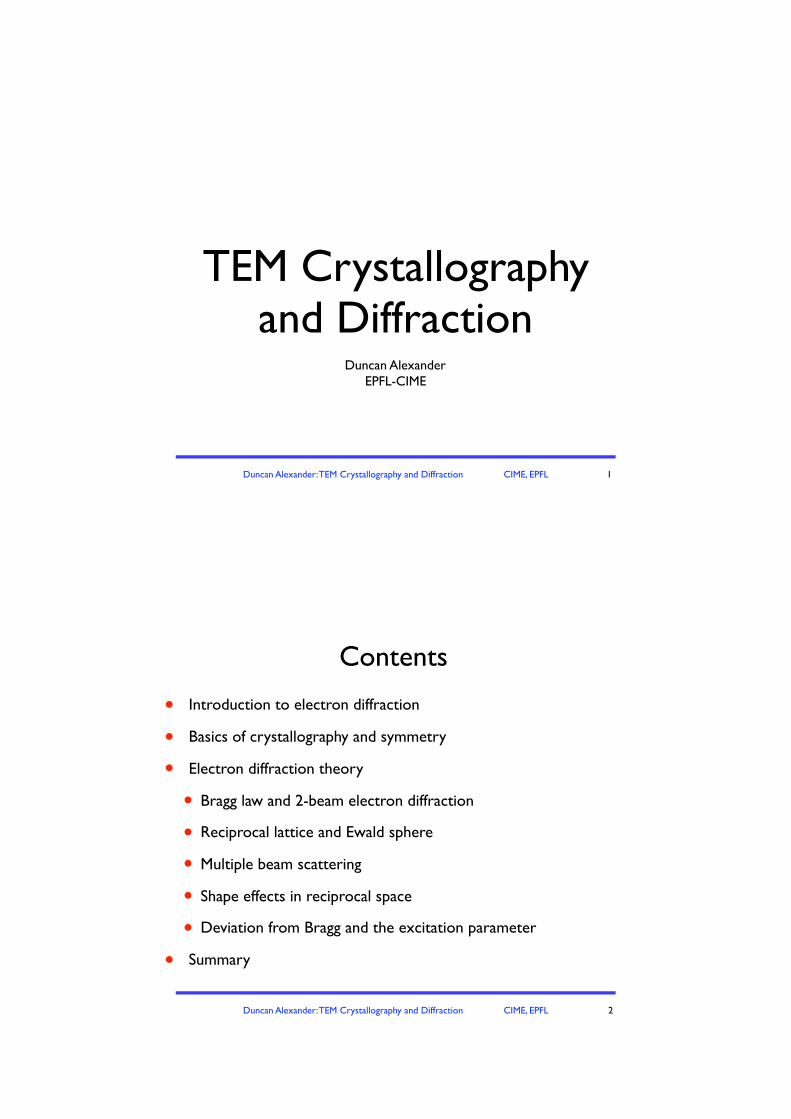
Contents
• Introduction to electron diffraction
• Basics of crystallography and symmetry
• Electron diffraction theory
• Bragg law and 2-beam electron diffraction
• Reciprocal lattice and Ewald sphere
• Multiple beam scattering
• Shape effects in reciprocal space
• Deviation from Bragg and the excitation parameter
• Summary
2
Duncan Alexander: TEM Crystallography and Diffraction CIME, EPFL
Introduction to electron diffraction
3
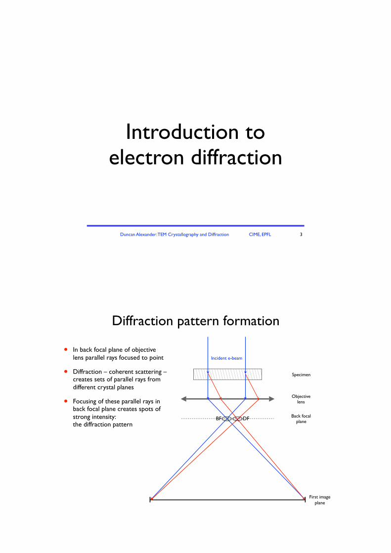
Diffraction pattern formation
Incident e-beam
Specimen
Objective lens
Back focalplane
First imageplane
BF DF
• In back focal plane of objective lens parallel rays focused to point
• Diffraction – coherent scattering – creates sets of parallel rays from different crystal planes
• Focusing of these parallel rays in back focal plane creates spots of strong intensity:!the diffraction pattern
Duncan Alexander: TEM Crystallography and Diffraction CIME, EPFL
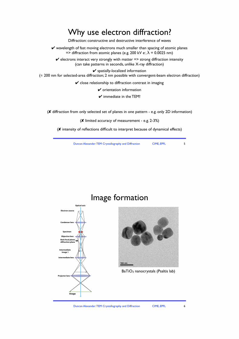
Diffraction: constructive and destructive interference of waves
✔ electrons interact very strongly with matter => strong diffraction intensity (can take patterns in seconds, unlike X-ray diffraction)
✘ diffraction from only selected set of planes in one pattern - e.g. only 2D information
✔ wavelength of fast moving electrons much smaller than spacing of atomic planes => diffraction from atomic planes (e.g. 200 kV e-, λ = 0.0025 nm)
✔ spatially-localized information(≳ 200 nm for selected-area diffraction; 2 nm possible with convergent-beam electron diffraction)
✔ orientation information
✔ close relationship to diffraction contrast in imaging
✔ immediate in the TEM!
✘ limited accuracy of measurement - e.g. 2-3%
✘ intensity of reflections difficult to interpret because of dynamical effects
Why use electron diffraction?
5
(✘ diffraction from only selected set of planes in one pattern - e.g. only 2D information)
(✘ limited accuracy of measurement - e.g. 2-3%)
(✘ intensity of reflections difficult to interpret because of dynamical effects)
Duncan Alexander: TEM Crystallography and Diffraction CIME, EPFL
Optical axis
Electron source
Condenser lens
Specimen
Objective lens
Back focal plane/diffraction plane
Intermediate lens
Projector lens
Image
Intermediate image 1
BaTiO3 nanocrystals (Psaltis lab)
Image formation
6
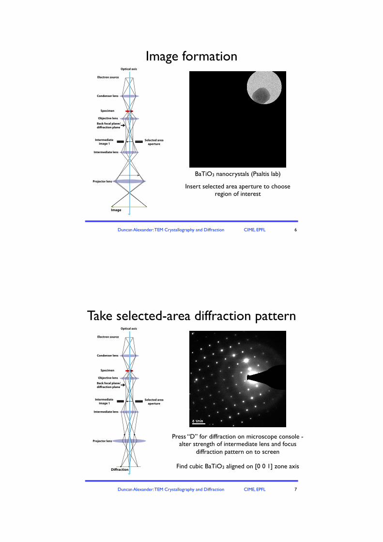
Duncan Alexander: TEM Crystallography and Diffraction CIME, EPFL
Insert selected area aperture to choose region of interest
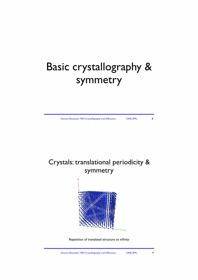
Optical axis
Electron source
Condenser lens
Specimen
Objective lens
Back focal plane/diffraction plane
Intermediate lens
Projector lens
Image
Intermediate image 1
Optical axis
Electron source
Condenser lens
Specimen
Objective lens
Back focal plane/diffraction plane
Intermediate lens
Projector lens
Image
Intermediate image 1
Selected areaaperture
BaTiO3 nanocrystals (Psaltis lab)
Image formation
6
Duncan Alexander: TEM Crystallography and Diffraction CIME, EPFL
Press “D” for diffraction on microscope console - alter strength of intermediate lens and focus
diffraction pattern on to screen
Optical axis
Electron source
Condenser lens
Specimen
Objective lens
Back focal plane/diffraction plane
Intermediate lens
Projector lens
Image
Intermediate image 1
Selected areaaperture
Optical axis
Electron source
Condenser lens
Specimen
Objective lens
Back focal plane/diffraction plane
Intermediate lens
Projector lens
Diffraction
Intermediate image 1
Selected areaaperture
Find cubic BaTiO3 aligned on [0 0 1] zone axis
Take selected-area diffraction pattern
7
Duncan Alexander: TEM Crystallography and Diffraction CIME, EPFL
Basic crystallography & symmetry
8
Duncan Alexander: TEM Crystallography and Diffraction CIME, EPFL
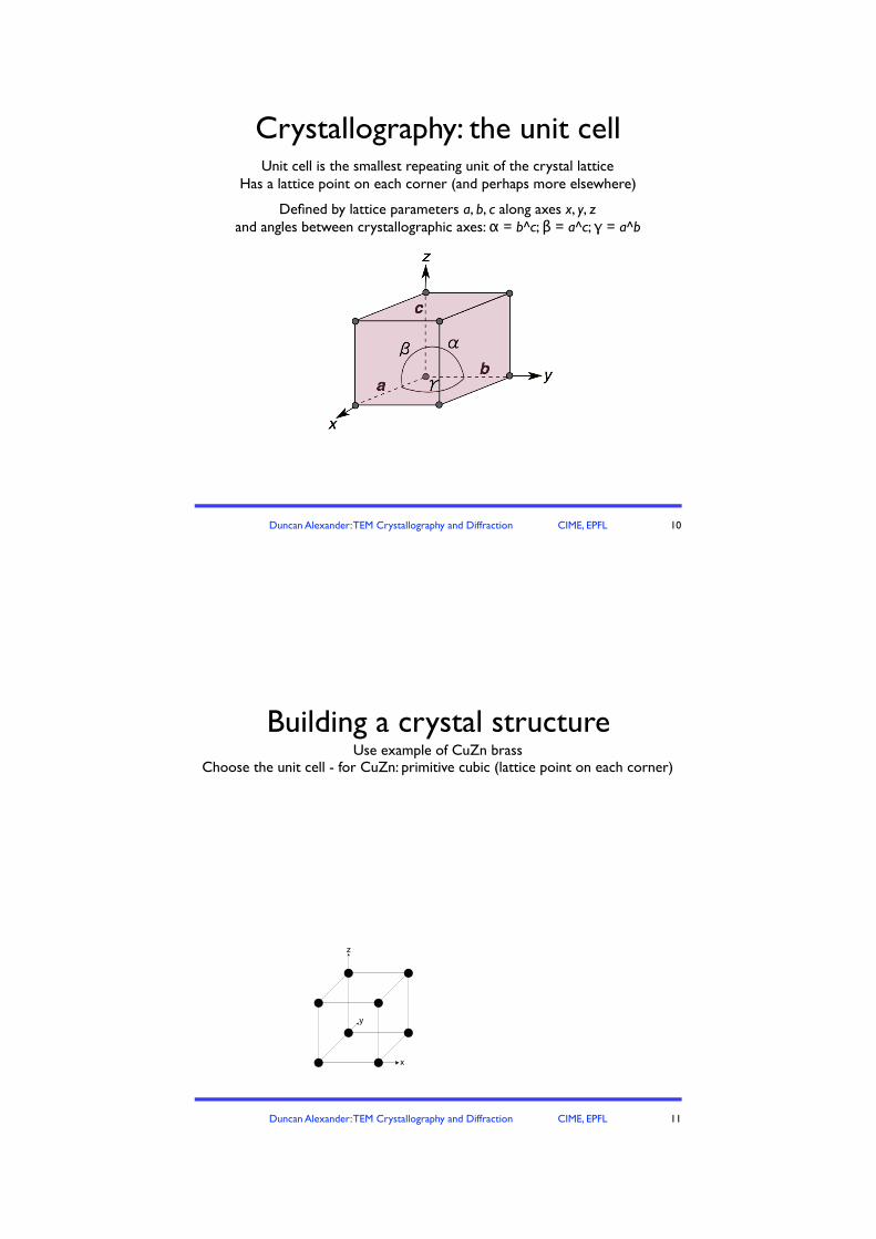
Repetition of translated structure to infinity
Crystals: translational periodicity & symmetry
9
Duncan Alexander: TEM Crystallography and Diffraction CIME, EPFL
Unit cell is the smallest repeating unit of the crystal latticeHas a lattice point on each corner (and perhaps more elsewhere)
Defined by lattice parameters a, b, c along axes x, y, z!and angles between crystallographic axes: # = b^c; $ = a^c; % = a^b
Crystallography: the unit cell
10
Duncan Alexander: TEM Crystallography and Diffraction CIME, EPFL
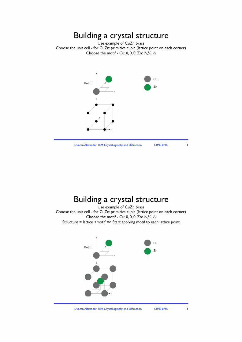
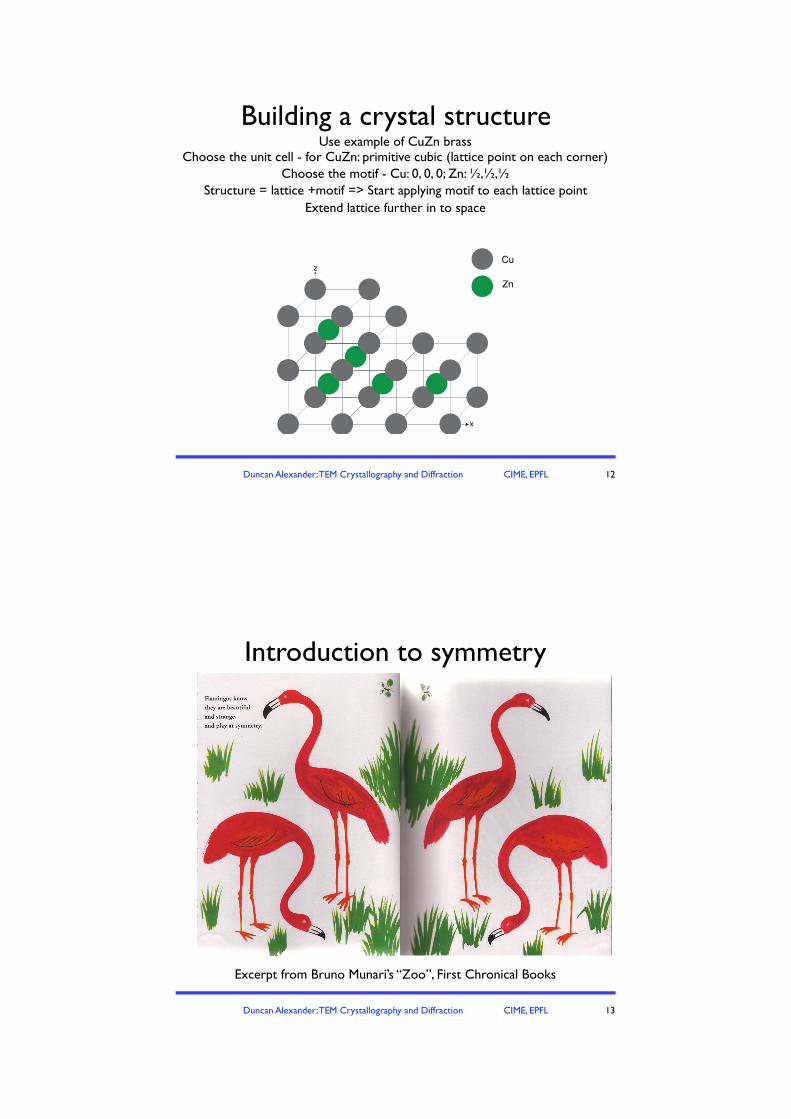
Use example of CuZn brassChoose the unit cell - for CuZn: primitive cubic (lattice point on each corner)
x
y
z
Building a crystal structure
11
Duncan Alexander: TEM Crystallography and Diffraction CIME, EPFL
Use example of CuZn brassChoose the unit cell - for CuZn: primitive cubic (lattice point on each corner)
x
y
z
Choose the motif - Cu: 0, 0, 0; Zn: ½,½,½
x
y
z
Motif:Cu
Znx
y
z
Building a crystal structure
11
Duncan Alexander: TEM Crystallography and Diffraction CIME, EPFL
Use example of CuZn brassChoose the unit cell - for CuZn: primitive cubic (lattice point on each corner)
x
y
z
Choose the motif - Cu: 0, 0, 0; Zn: ½,½,½
x
y
z
Motif:Cu
Znx
y
z
Structure = lattice +motif => Start applying motif to each lattice point
x
y
z
Motif:Cu
Znx
y
z
x
y
z
Motif:Cu
Znx
y
z
Building a crystal structure
11
Duncan Alexander: TEM Crystallography and Diffraction CIME, EPFL
x
y
z
Motif:Cu
Znx
y
z
Use example of CuZn brassChoose the unit cell - for CuZn: primitive cubic (lattice point on each corner)
Choose the motif - Cu: 0, 0, 0; Zn: ½,½,½Structure = lattice +motif => Start applying motif to each lattice point
Extend lattice further in to space
x
y
z
Cu
Zn
x
y
z
Cu
Zn
x
y
z
Cu
Zn
y
x
y
zCu
Zn
y
y
x
y
zCu
Zn
y
y
y
x
y
zCu
Zn
y
y
y
y
Building a crystal structure
12
Duncan Alexander: TEM Crystallography and Diffraction CIME, EPFL
Introduction to symmetry
13
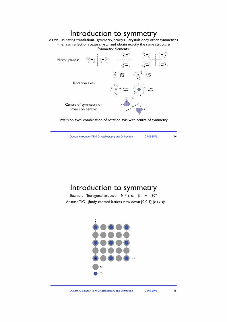
Flamingos knowthey are beautifuland strange,and play at symmetry.
\,t4r
lTal
\/' \ /\ / \ / I V \ 1 \ X Y \ \
qr
lt\-4l
Excerpt from Bruno Munari’s “Zoo”, First Chronical Books
Duncan Alexander: TEM Crystallography and Diffraction CIME, EPFL
As well as having translational symmetry, nearly all crystals obey other symmetries !- i.e. can reflect or rotate crystal and obtain exactly the same structure
Symmetry elements:
Mirror planes:
Symmetry elements:
Rotation axes:
Inversion axes: combination of rotation axis with centre of symmetry
Centre of symmetry orinversion centre:
Introduction to symmetry
14
Duncan Alexander: TEM Crystallography and Diffraction CIME, EPFL
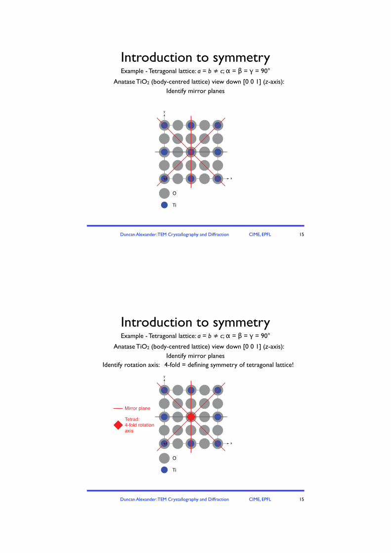
Example - Tetragonal lattice: a = b & c; # = $ = % = 90°
Anatase TiO2 (body-centred lattice) view down [0 0 1] (z-axis):
x
y
z
O
Ti
x
y
z
O
Ti
Introduction to symmetry
15
Duncan Alexander: TEM Crystallography and Diffraction CIME, EPFL
Example - Tetragonal lattice: a = b ≠ c; α = β = γ = 90°
Anatase TiO2 (body-centred lattice) view down [0 0 1] (z-axis):
x
y
z
O
Ti
x
y
z
O
Ti
Identify mirror planes
x
y
z
O
Ti
x
y
z
O
Ti
x
y
z
O
Ti
x
y
z
O
Ti
x
y
z
O
Ti
x
y
z
O
Ti
Tetrad:4-fold rotationaxis
Mirror plane
Identify rotation axis: 4-fold = defining symmetry of tetragonal lattice!
Introduction to symmetry
15
Duncan Alexander: TEM Crystallography and Diffraction CIME, EPFL
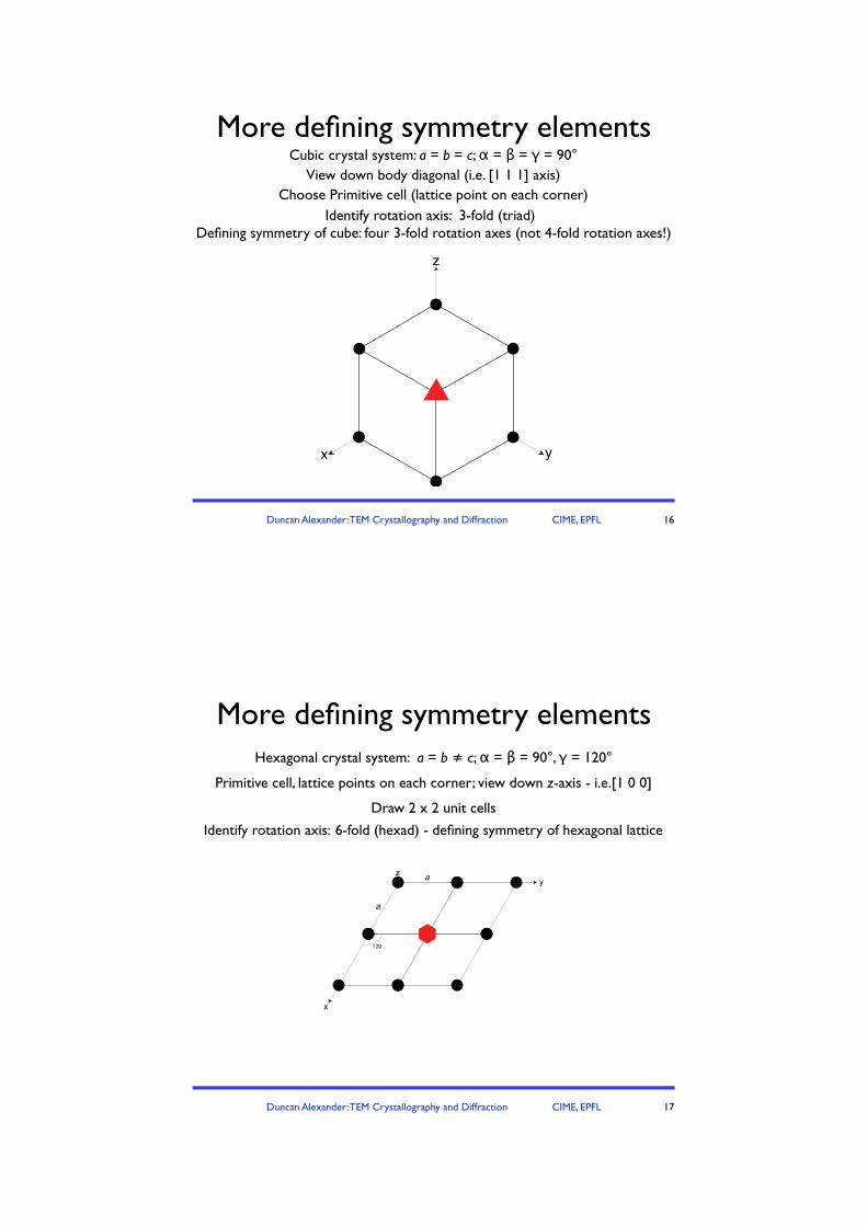
Cubic crystal system: a = b = c; α = β = γ = 90°View down body diagonal (i.e. [1 1 1] axis)
Choose Primitive cell (lattice point on each corner)Identify rotation axis: 3-fold (triad)
Defining symmetry of cube: four 3-fold rotation axes (not 4-fold rotation axes!)
x y
z
x y
z
x y
z
More defining symmetry elements
16
Duncan Alexander: TEM Crystallography and Diffraction CIME, EPFL
Hexagonal crystal system: a = b ≠ c; α = β = 90°, γ = 120°
Primitive cell, lattice points on each corner; view down z-axis - i.e.[1 0 0]
x
yz
120
a
a
Draw 2 x 2 unit cells
Identify rotation axis: 6-fold (hexad) - defining symmetry of hexagonal lattice
x
yz
120
a
a
x
yz
120
a
a
More defining symmetry elements
17
Duncan Alexander: TEM Crystallography and Diffraction CIME, EPFL
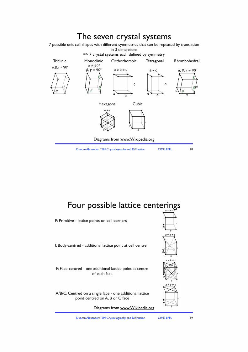
7 possible unit cell shapes with different symmetries that can be repeated by translation in 3 dimensions!
=> 7 crystal systems each defined by symmetry
Triclinic Monoclinic Orthorhombic Tetragonal Rhombohedral
Hexagonal Cubic
Diagrams from www.Wikipedia.org
The seven crystal systems
18
Duncan Alexander: TEM Crystallography and Diffraction CIME, EPFL
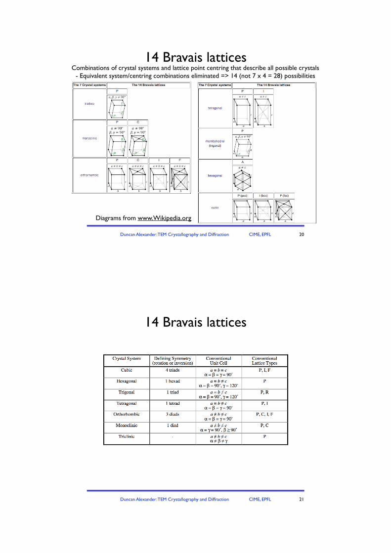
P: Primitive - lattice points on cell corners
I: Body-centred - additional lattice point at cell centre
F: Face-centred - one additional lattice point at centre !of each face
A/B/C: Centred on a single face - one additional lattice!point centred on A, B or C face
Diagrams from www.Wikipedia.org
Four possible lattice centerings
19
Duncan Alexander: TEM Crystallography and Diffraction CIME, EPFL
Combinations of crystal systems and lattice point centring that describe all possible crystals!- Equivalent system/centring combinations eliminated => 14 (not 7 x 4 = 28) possibilities
Diagrams from www.Wikipedia.org
14 Bravais lattices
20
Duncan Alexander: TEM Crystallography and Diffraction CIME, EPFL
14 Bravais lattices
21
Duncan Alexander: TEM Crystallography and Diffraction CIME, EPFL
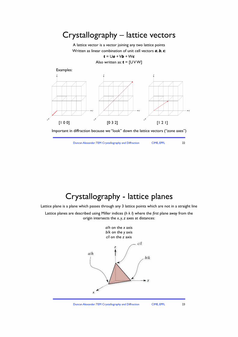
A lattice vector is a vector joining any two lattice pointsWritten as linear combination of unit cell vectors a, b, c:
t = Ua + Vb + WcAlso written as: t = [U V W]
Examples:z
x
y
z
x
y
z
x
y
[1 0 0] [0 3 2] [1 2 1]
Important in diffraction because we “look” down the lattice vectors (“zone axes”)
Crystallography – lattice vectors
22
Duncan Alexander: TEM Crystallography and Diffraction CIME, EPFL
Lattice plane is a plane which passes through any 3 lattice points which are not in a straight line
Lattice planes are described using Miller indices (h k l) where the first plane away from the !origin intersects the x, y, z axes at distances:
a/h on the x axisb/k on the y axisc/l on the z axis
Crystallography - lattice planes
23
Duncan Alexander: TEM Crystallography and Diffraction CIME, EPFL
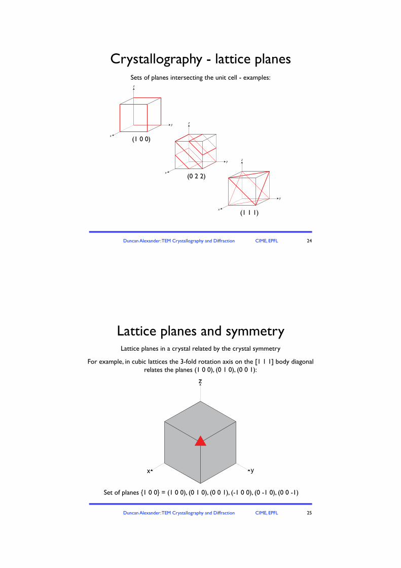
Sets of planes intersecting the unit cell - examples:
x
z
y
x
z
y
x
z
y
(1 0 0)
(0 2 2)
(1 1 1)
Crystallography - lattice planes
24
Duncan Alexander: TEM Crystallography and Diffraction CIME, EPFL
Lattice planes in a crystal related by the crystal symmetry
For example, in cubic lattices the 3-fold rotation axis on the [1 1 1] body diagonalrelates the planes (1 0 0), (0 1 0), (0 0 1):
x y
z
x y
z
x y
z
x y
z
x y
z
Set of planes {1 0 0} = (1 0 0), (0 1 0), (0 0 1), (-1 0 0), (0 -1 0), (0 0 -1)
Lattice planes and symmetry
25
Duncan Alexander: TEM Crystallography and Diffraction CIME, EPFL
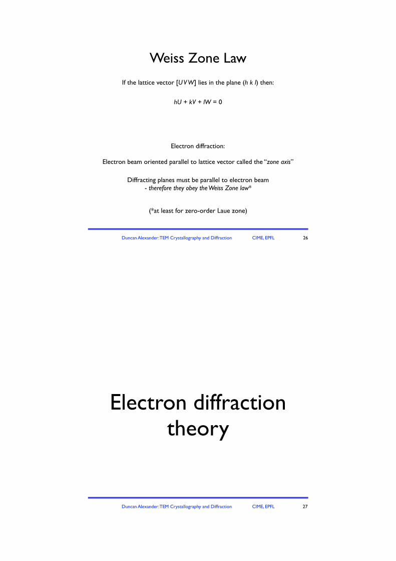
If the lattice vector [U V W] lies in the plane (h k l) then:
hU + kV + lW = 0
Electron diffraction:
Electron beam oriented parallel to lattice vector called the “zone axis”
Diffracting planes must be parallel to electron beam- therefore they obey the Weiss Zone law*
(*at least for zero-order Laue zone)
Weiss Zone Law
26
Duncan Alexander: TEM Crystallography and Diffraction CIME, EPFL
Electron diffraction theory
27
Duncan Alexander: TEM Crystallography and Diffraction CIME, EPFL
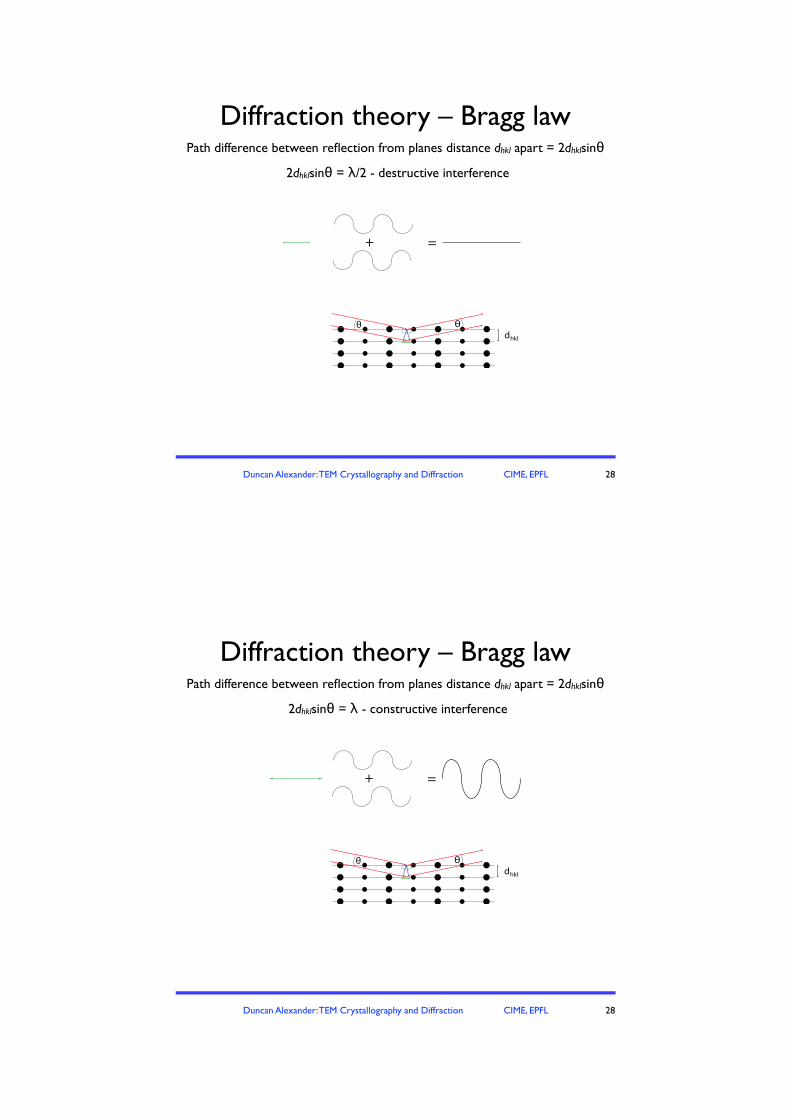
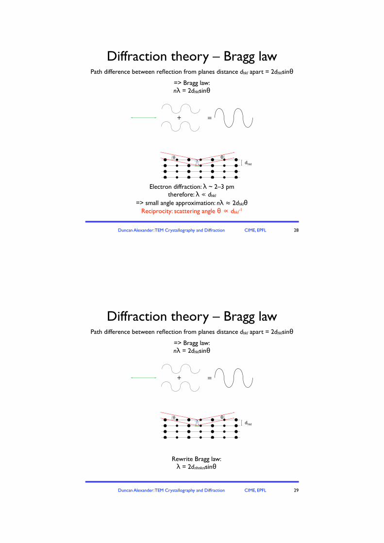
Path difference between reflection from planes distance dhkl apart = 2dhklsinθ
dhkldθ
hkldθ θ
hkldθ θ
hkldθ θ
hkldθ θ
+ =
hkl
2dhklsinθ = λ/2 - destructive interference
Diffraction theory – Bragg law
28
Duncan Alexander: TEM Crystallography and Diffraction CIME, EPFL
Path difference between reflection from planes distance dhkl apart = 2dhklsinθ
dhkldθ
hkldθ θ
hkldθ θ
hkldθ θ
hkldθ θ
+ =
hkldθ θ
+ =
hkl
2dhklsinθ = λ/2 - destructive interference2dhklsinθ = λ - constructive interference
Diffraction theory – Bragg law
28
Duncan Alexander: TEM Crystallography and Diffraction CIME, EPFL
Path difference between reflection from planes distance dhkl apart = 2dhklsinθ
Electron diffraction: λ ~ 2–3 pmtherefore: λ ≪ dhkl
=> small angle approximation: nλ ≈ 2dhklθReciprocity: scattering angle θ ∝ dhkl-1
dhkldθ
hkldθ θ
hkldθ θ
hkldθ θ
hkldθ θ
+ =
hkldθ θ
+ =
hkl
2dhklsinθ = λ/2 - destructive interference2dhklsinθ = λ - constructive interference=> Bragg law:nλ = 2dhklsinθ
Diffraction theory – Bragg law
28
Duncan Alexander: TEM Crystallography and Diffraction CIME, EPFL
Path difference between reflection from planes distance dhkl apart = 2dhklsinθ
dhkldθ
hkldθ θ
hkldθ θ
hkldθ θ
hkldθ θ
+ =
hkldθ θ
+ =
hkl
2dhklsinθ = λ/2 - destructive interference2dhklsinθ = λ - constructive interference=> Bragg law:nλ = 2dhklsinθ
Rewrite Bragg law:λ = 2dnhnknlsinθ
Diffraction theory – Bragg law
29
Duncan Alexander: TEM Crystallography and Diffraction CIME, EPFL
d
θ
θ
hkl
Diffraction theory – 2-beam condition
30
Duncan Alexander: TEM Crystallography and Diffraction CIME, EPFL
d
θ
θ
hkl
θ
θ
θ
θθ
k I
θ
θθ
k I
k D
k I
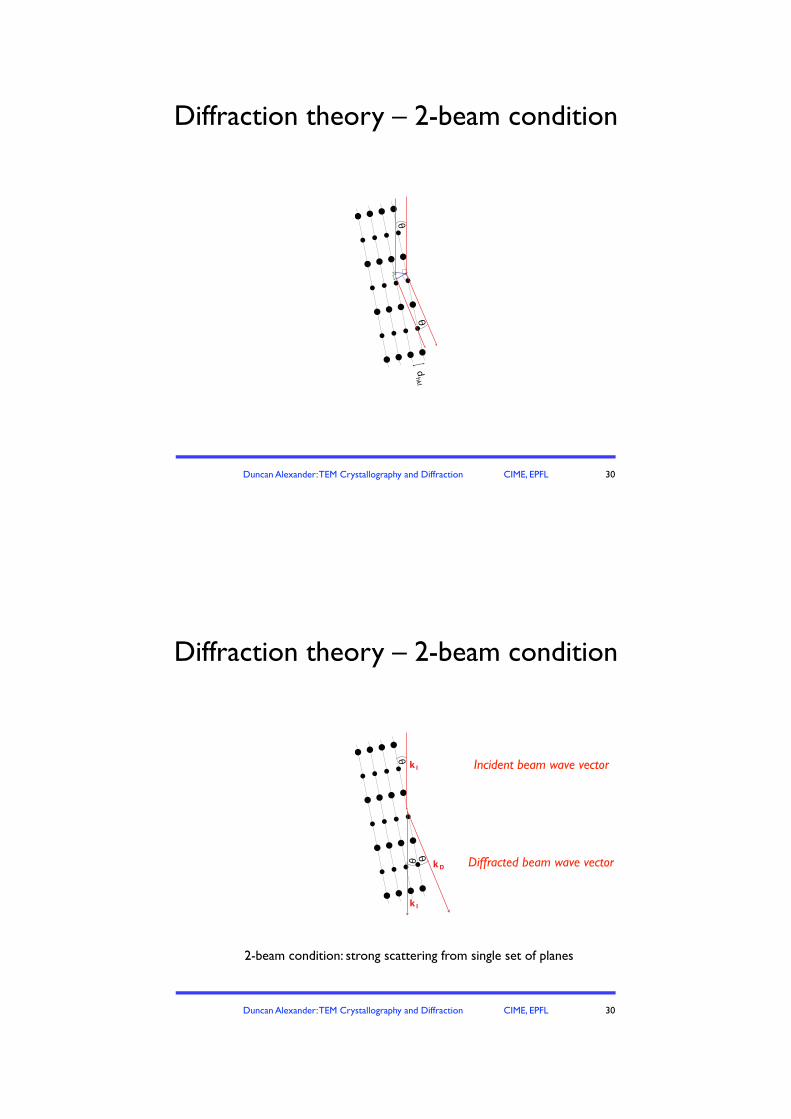
2-beam condition: strong scattering from single set of planes
Diffraction theory – 2-beam condition
30
Incident beam wave vector
Diffracted beam wave vector
Duncan Alexander: TEM Crystallography and Diffraction CIME, EPFL
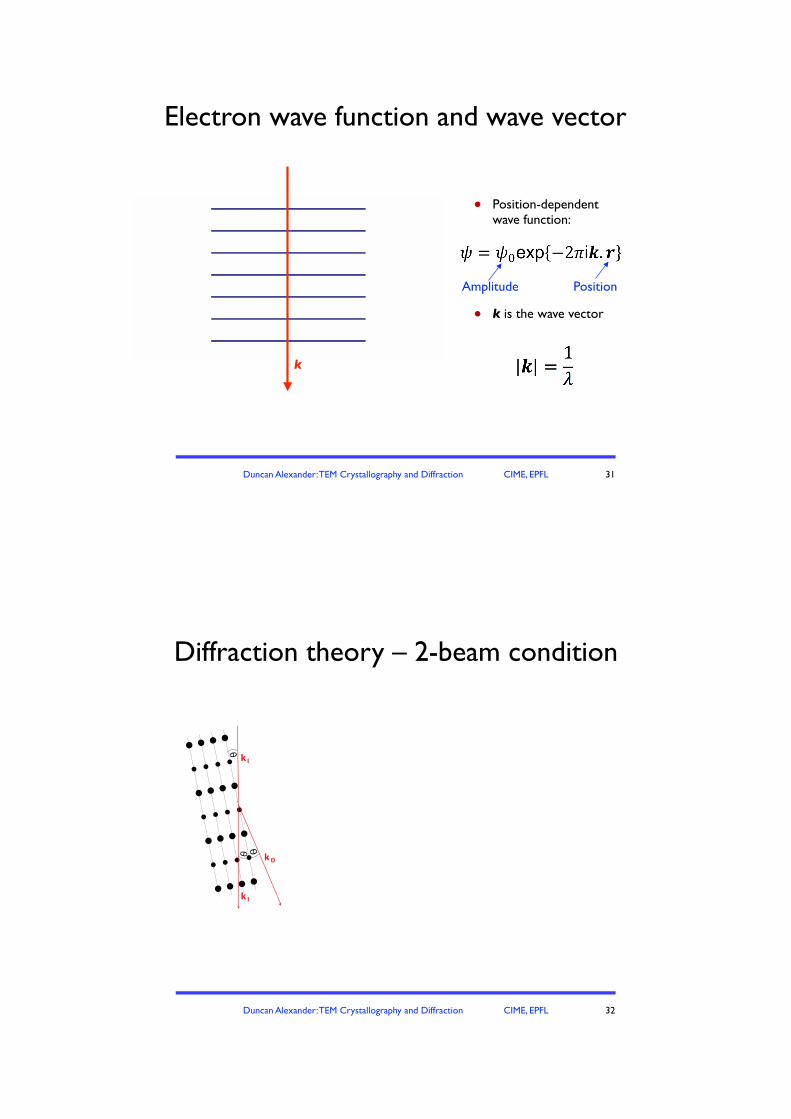
Electron wave function and wave vector
31
' Position-dependent!wave function:
' k is the wave vector
Amplitude Position
k
Duncan Alexander: TEM Crystallography and Diffraction CIME, EPFL
d
θ
θ
hkl
θ
θ
θ
θθ
k I
θ
θθ
k I
k D
k I
32
Diffraction theory – 2-beam condition
Duncan Alexander: TEM Crystallography and Diffraction CIME, EPFL
d
θ
θ
hkl
θ
θ
θ
θθ
k I
θ
θθ
k I
k D
k I
θ
θ
0 0 0 Gg
θ
k I
k D
k I
32
Diffraction theory – 2-beam condition
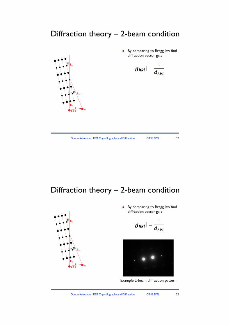
! By comparing to Bragg law find diffraction vector ghkl:
Duncan Alexander: TEM Crystallography and Diffraction CIME, EPFL
d
θ
θ
hkl
θ
θ
θ
θθ
k I
θ
θθ
k I
k D
k I
θ
θ
0 0 0 Gg
θ
k I
k D
k I
32
Diffraction theory – 2-beam condition
' By comparing to Bragg law find diffraction vector ghkl:
Example 2-beam diffraction pattern
Duncan Alexander: TEM Crystallography and Diffraction CIME, EPFL
d
θ
θ
hkl
θ
θ
θ
θθ
k I
θ
θθ
k I
k D
k I
θ
θ
0 0 0 Gg
θ
k I
k D
k I
33
Diffraction theory – 2-beam condition
' By comparing to Bragg law find diffraction vector ghkl:
' Small angle approximation
Important because scattering angles are essentially linear with reciprocal spacing in TEM, and so plane spacings are
easy to measure from diffraction patterns!
Duncan Alexander: TEM Crystallography and Diffraction CIME, EPFL
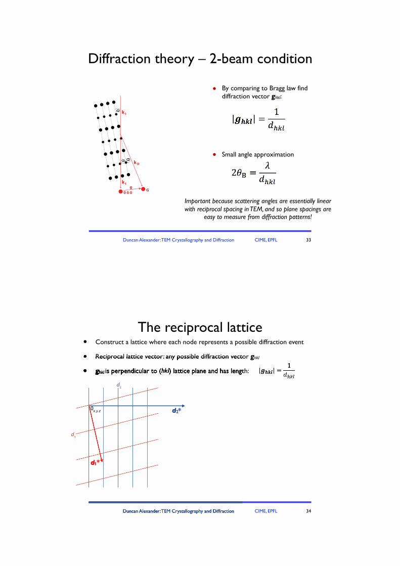
The reciprocal lattice• Construct a lattice where each node represents a possible diffraction event
• Reciprocal lattice vector: any possible diffraction vector ghkl
• ghkl is perpendicular to (hkl) lattice plane and has length:
34
d1*
d2*
Duncan Alexander: TEM Crystallography and Diffraction CIME, EPFL
• Reciprocal lattice vector: any possible diffraction vector
• ghkl ghkl g is perpendicular to (hkl) lattice plane and has length: hkl) lattice plane and has length: hkl
d1*
d2*
Duncan Alexander: TEM Crystallography and Diffraction CIME, EPFL
The reciprocal lattice• Add plane d3 with (h3 k3 l3) which is related to planes
d1 with (h1 k1 l1) and d2 with (h2 k2 l2) by:
35
d1*
d2*
Duncan Alexander: TEM Crystallography and Diffraction CIME, EPFL
with ( 1) with ( 2) by:
d1*
d2*
d3*
• In this case find:
d3* = d1* + d2*
(h3 k3 l3) = (h1+h2 k1+k2 l1+l2)
Duncan Alexander: TEM Crystallography and Diffraction CIME, EPFL
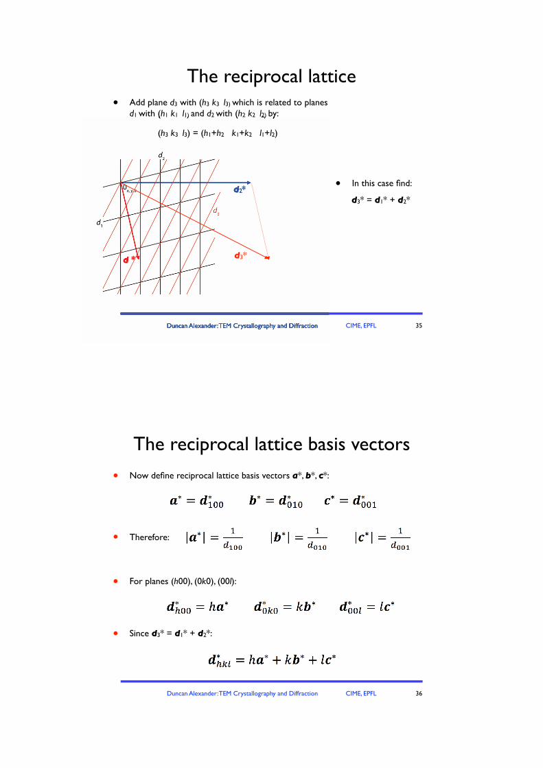
The reciprocal lattice basis vectors
• Now define reciprocal lattice basis vectors a*, b*, c*:
36
• Therefore:
• For planes (h00), (0k0), (00l):
• Since d3* = d1* + d2*:
Duncan Alexander: TEM Crystallography and Diffraction CIME, EPFL
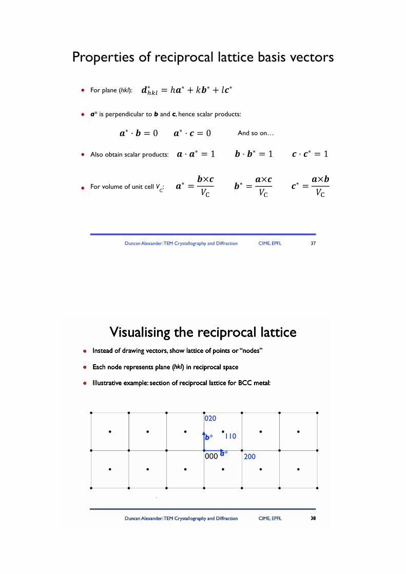
' For plane (hkl):
' a* is perpendicular to b and c, hence scalar products:
' Also obtain scalar products:
' For volume of unit cell VC:
Properties of reciprocal lattice basis vectors
37
And so on…
Duncan Alexander: TEM Crystallography and Diffraction CIME, EPFL
Visualising the reciprocal lattice
38
' Instead of drawing vectors, show lattice of points or “nodes”
' Each node represents plane (hkl) in reciprocal space
' Illustrative example: section of reciprocal lattice for BCC metal:
Duncan Alexander: TEM Crystallography and Diffraction CIME, EPFL
Visualising the reciprocal lattice
38
' Instead of drawing vectors, show lattice of points or “nodes”
' Each node represents plane (hkl) in reciprocal spacehkl) in reciprocal spacehkl
' Illustrative example: section of reciprocal lattice for BCC metal:
200
020
110
a*
b*
Duncan Alexander: TEM Crystallography and Diffraction CIME, EPFL
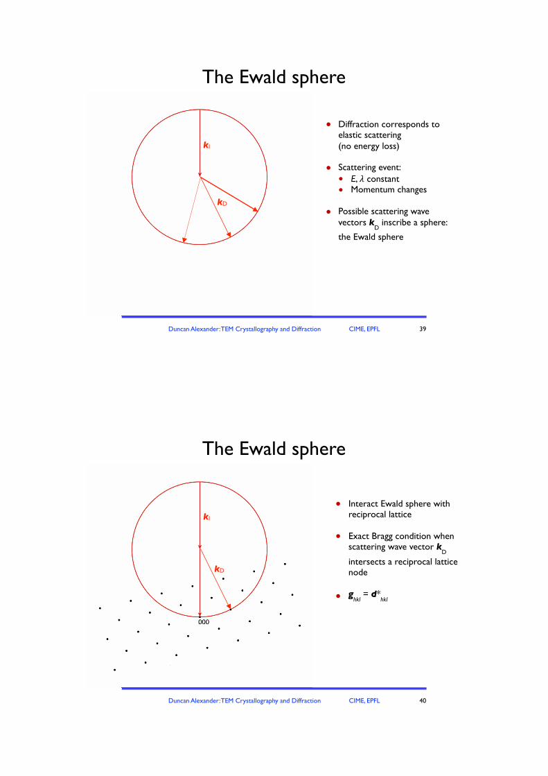
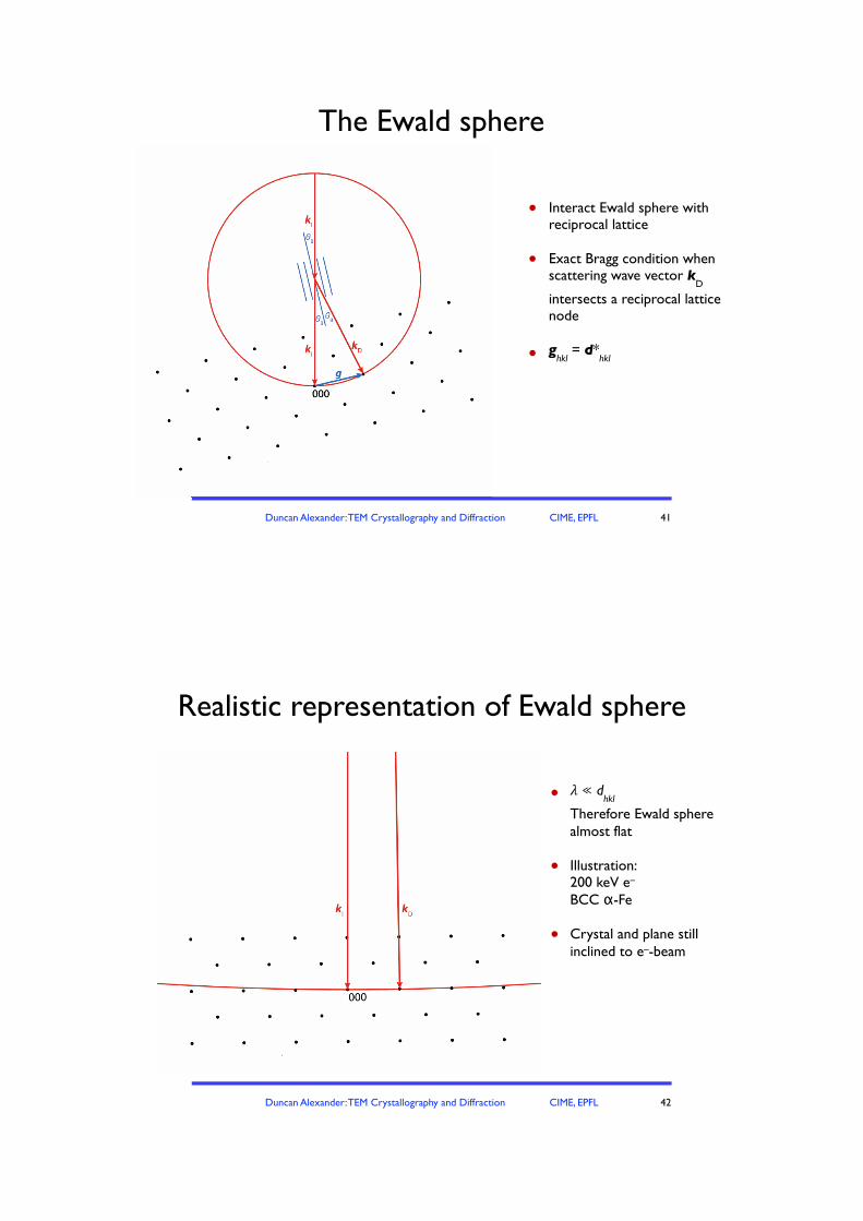
The Ewald sphere
39
' Diffraction corresponds to elastic scattering!(no energy loss)
' Scattering event:' E, ! constant' Momentum changes
' Possible scattering wave vectors k
D inscribe a sphere:
the Ewald sphere
kI
kD
Duncan Alexander: TEM Crystallography and Diffraction CIME, EPFL
The Ewald sphere
40
' Interact Ewald sphere with reciprocal lattice
' Exact Bragg condition when scattering wave vector k
D
intersects a reciprocal lattice node
' ghkl
= d*hkl
kI
kD
Duncan Alexander: TEM Crystallography and Diffraction CIME, EPFL
The Ewald sphere
41
' Interact Ewald sphere with reciprocal lattice
' Exact Bragg condition when scattering wave vector k
D
intersects a reciprocal lattice node
' ghkl
= d*hkl
Duncan Alexander: TEM Crystallography and Diffraction CIME, EPFL
Realistic representation of Ewald sphere
42
' ! " dhkl
!Therefore Ewald sphere almost flat
' Illustration:!200 keV e–!BCC #-Fe
' Crystal and plane still inclined to e–-beam
Duncan Alexander: TEM Crystallography and Diffraction CIME, EPFL
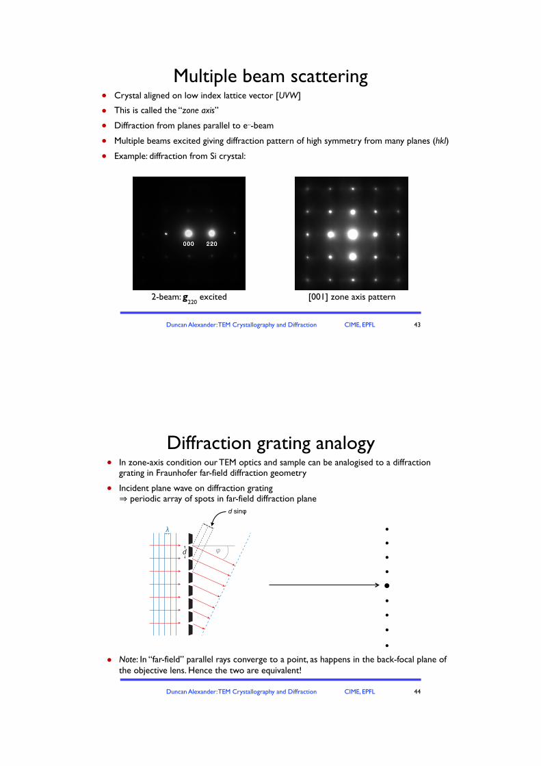
Multiple beam scattering
43
2-beam: g220
excited [001] zone axis pattern
! Crystal aligned on low index lattice vector [UVW]
! This is called the “zone axis”
! Diffraction from planes parallel to e–-beam
! Multiple beams excited giving diffraction pattern of high symmetry from many planes (hkl)
! Example: diffraction from Si crystal:
Duncan Alexander: TEM Crystallography and Diffraction CIME, EPFL
Diffraction grating analogy
44
! In zone-axis condition our TEM optics and sample can be analogised to a diffraction grating in Fraunhofer far-field diffraction geometry
! Incident plane wave on diffraction grating"⇒ periodic array of spots in far-field diffraction plane
φ
λ
d
!"
"
"
""
"
"
"
"
!
!
!
!
!
!
!
!
d sin!
! Note: In “far-field” parallel rays converge to a point, as happens in the back-focal plane of the objective lens. Hence the two are equivalent!

Duncan Alexander: TEM Crystallography and Diffraction CIME, EPFL
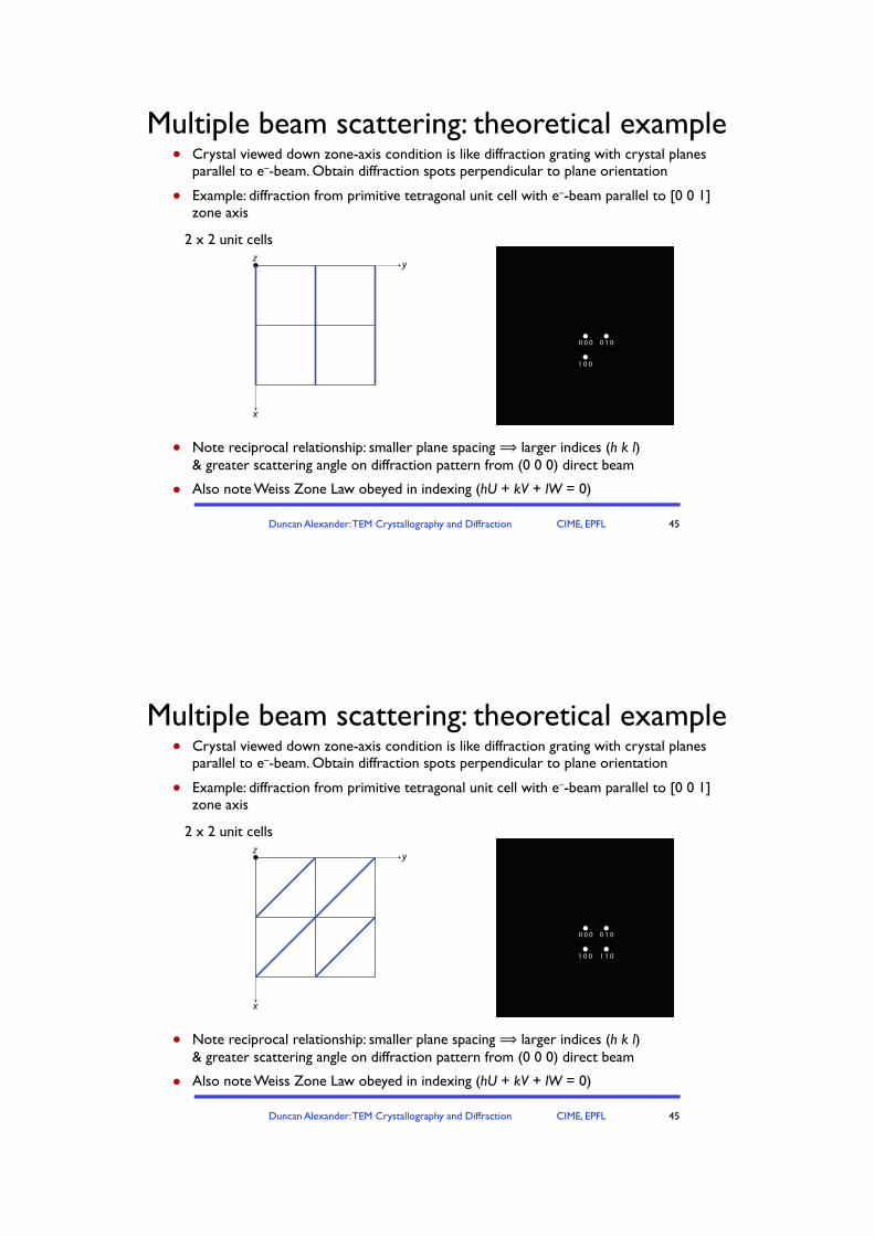
Multiple beam scattering: theoretical example
45
● Crystal viewed down zone-axis condition is like diffraction grating with crystal planes parallel to e–-beam. Obtain diffraction spots perpendicular to plane orientation
● Example: diffraction from primitive tetragonal unit cell with e–-beam parallel to [0 0 1] zone axis
x
yz
0 0 0
2 x 2 unit cells
● Note reciprocal relationship: smaller plane spacing ⟹ larger indices (h k l)& greater scattering angle on diffraction pattern from (0 0 0) direct beam
● Also note Weiss Zone Law obeyed in indexing (hU + kV + lW = 0)
Duncan Alexander: TEM Crystallography and Diffraction CIME, EPFL
Multiple beam scattering: theoretical example
45
● Crystal viewed down zone-axis condition is like diffraction grating with crystal planes parallel to e–-beam. Obtain diffraction spots perpendicular to plane orientation
● Example: diffraction from primitive tetragonal unit cell with e–-beam parallel to [0 0 1] zone axis
x
yz
x
yz
0 0 00 0 0
1 0 0
2 x 2 unit cells
● Note reciprocal relationship: smaller plane spacing ⟹ larger indices (h k l)& greater scattering angle on diffraction pattern from (0 0 0) direct beam
● Also note Weiss Zone Law obeyed in indexing (hU + kV + lW = 0)
Duncan Alexander: TEM Crystallography and Diffraction CIME, EPFL
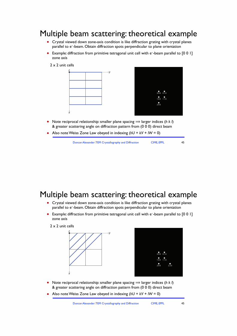
Multiple beam scattering: theoretical example
45
● Crystal viewed down zone-axis condition is like diffraction grating with crystal planes parallel to e–-beam. Obtain diffraction spots perpendicular to plane orientation
● Example: diffraction from primitive tetragonal unit cell with e–-beam parallel to [0 0 1] zone axis
x
yz
x
yz
0 0 00 0 0
1 0 0
x
yz
0 0 0
1 0 0
0 1 0
2 x 2 unit cells
● Note reciprocal relationship: smaller plane spacing ⟹ larger indices (h k l)& greater scattering angle on diffraction pattern from (0 0 0) direct beam
● Also note Weiss Zone Law obeyed in indexing (hU + kV + lW = 0)
Duncan Alexander: TEM Crystallography and Diffraction CIME, EPFL
Multiple beam scattering: theoretical example
45
● Crystal viewed down zone-axis condition is like diffraction grating with crystal planes parallel to e–-beam. Obtain diffraction spots perpendicular to plane orientation
● Example: diffraction from primitive tetragonal unit cell with e–-beam parallel to [0 0 1] zone axis
x
yz
x
yz
0 0 00 0 0
1 0 0
x
yz
0 0 0
1 0 0
0 1 0
x
yz
0 0 0
1 0 0
0 1 0
1 1 0
2 x 2 unit cells
● Note reciprocal relationship: smaller plane spacing ⟹ larger indices (h k l)& greater scattering angle on diffraction pattern from (0 0 0) direct beam
● Also note Weiss Zone Law obeyed in indexing (hU + kV + lW = 0)
Duncan Alexander: TEM Crystallography and Diffraction CIME, EPFL
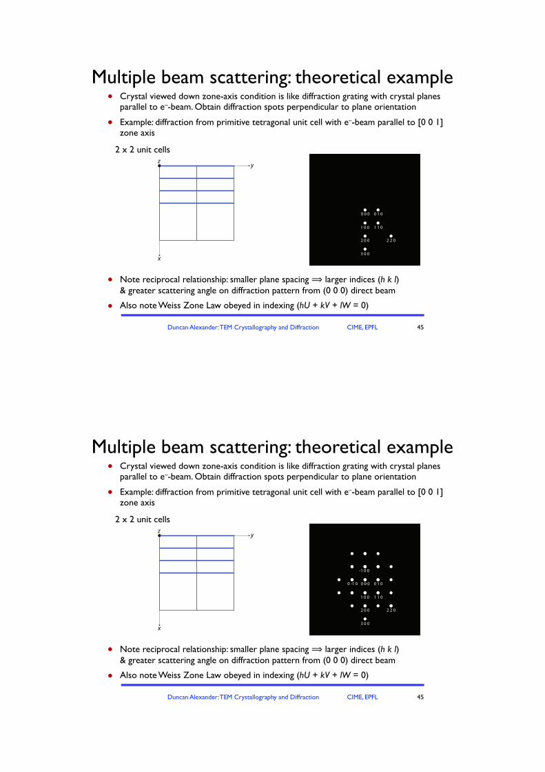
Multiple beam scattering: theoretical example
45
● Crystal viewed down zone-axis condition is like diffraction grating with crystal planes parallel to e–-beam. Obtain diffraction spots perpendicular to plane orientation
● Example: diffraction from primitive tetragonal unit cell with e–-beam parallel to [0 0 1] zone axis
x
yz
x
yz
0 0 00 0 0
1 0 0
x
yz
0 0 0
1 0 0
0 1 0
x
yz
0 0 0
1 0 0
0 1 0
1 1 0
x
yz
0 0 0
1 0 0
0 1 0
1 1 0
2 0 0
2 x 2 unit cells
● Note reciprocal relationship: smaller plane spacing ⟹ larger indices (h k l)& greater scattering angle on diffraction pattern from (0 0 0) direct beam
● Also note Weiss Zone Law obeyed in indexing (hU + kV + lW = 0)
Duncan Alexander: TEM Crystallography and Diffraction CIME, EPFL
Multiple beam scattering: theoretical example
45
● Crystal viewed down zone-axis condition is like diffraction grating with crystal planes parallel to e–-beam. Obtain diffraction spots perpendicular to plane orientation
● Example: diffraction from primitive tetragonal unit cell with e–-beam parallel to [0 0 1] zone axis
x
yz
x
yz
0 0 00 0 0
1 0 0
x
yz
0 0 0
1 0 0
0 1 0
x
yz
0 0 0
1 0 0
0 1 0
1 1 0
x
yz
0 0 0
1 0 0
0 1 0
1 1 0
2 0 0
x
yz
0 0 0
1 0 0
0 1 0
1 1 0
2 0 0 2 2 0
x
yz
2 x 2 unit cells
0 0 0
1 0 0
0 1 0
1 1 0
2 0 0 2 2 0
3 0 0
0 0 0
1 0 0
0 1 0
1 1 0
2 0 0 2 2 0
3 0 0
-1 0 0
0 -1 0
● Note reciprocal relationship: smaller plane spacing ⟹ larger indices (h k l)& greater scattering angle on diffraction pattern from (0 0 0) direct beam
● Also note Weiss Zone Law obeyed in indexing (hU + kV + lW = 0)
Duncan Alexander: TEM Crystallography and Diffraction CIME, EPFL
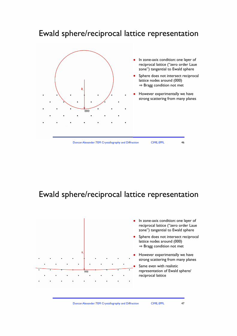
Ewald sphere/reciprocal lattice representation
46
' In zone-axis condition: one layer of reciprocal lattice (“zero order Laue zone”) tangential to Ewald sphere
' Sphere does not intersect reciprocal lattice nodes around (000)!⇒ Bragg condition not met
' However experimentally we have strong scattering from many planes
"
Duncan Alexander: TEM Crystallography and Diffraction CIME, EPFL
Ewald sphere/reciprocal lattice representation
47
' In zone-axis condition: one layer of reciprocal lattice (“zero order Laue zone”) tangential to Ewald sphere
' Sphere does not intersect reciprocal lattice nodes around (000)!⇒ Bragg condition not met
' However experimentally we have strong scattering from many planes
' Same even with realistic representation of Ewald sphere/reciprocal lattice
"
Duncan Alexander: TEM Crystallography and Diffraction CIME, EPFL
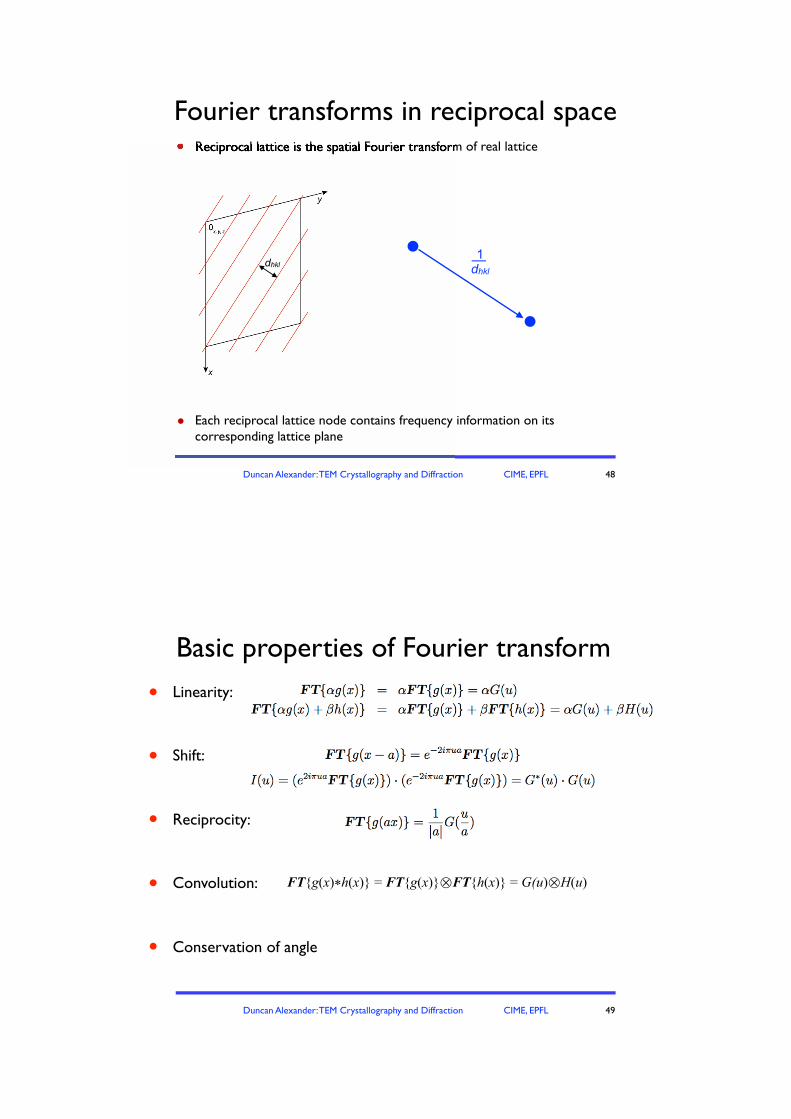
Fourier transforms in reciprocal space
48
' Reciprocal lattice is the spatial Fourier transform of real lattice' Reciprocal lattice is the spatial Fourier transform of real lattice
dhkl dhkl1––
' Each reciprocal lattice node contains frequency information on its corresponding lattice plane
Duncan Alexander: TEM Crystallography and Diffraction CIME, EPFL
Basic properties of Fourier transform
• Linearity:
• Shift:
• Reciprocity:
• Convolution:
• Conservation of angle
49
FT{g(x)*h(x)} = FT{g(x)}#FT{h(x)} = G(u)#H(u)
Duncan Alexander: TEM Crystallography and Diffraction CIME, EPFL
X
X “Relrod”
= 2 lengths scales in!reciprocal space!
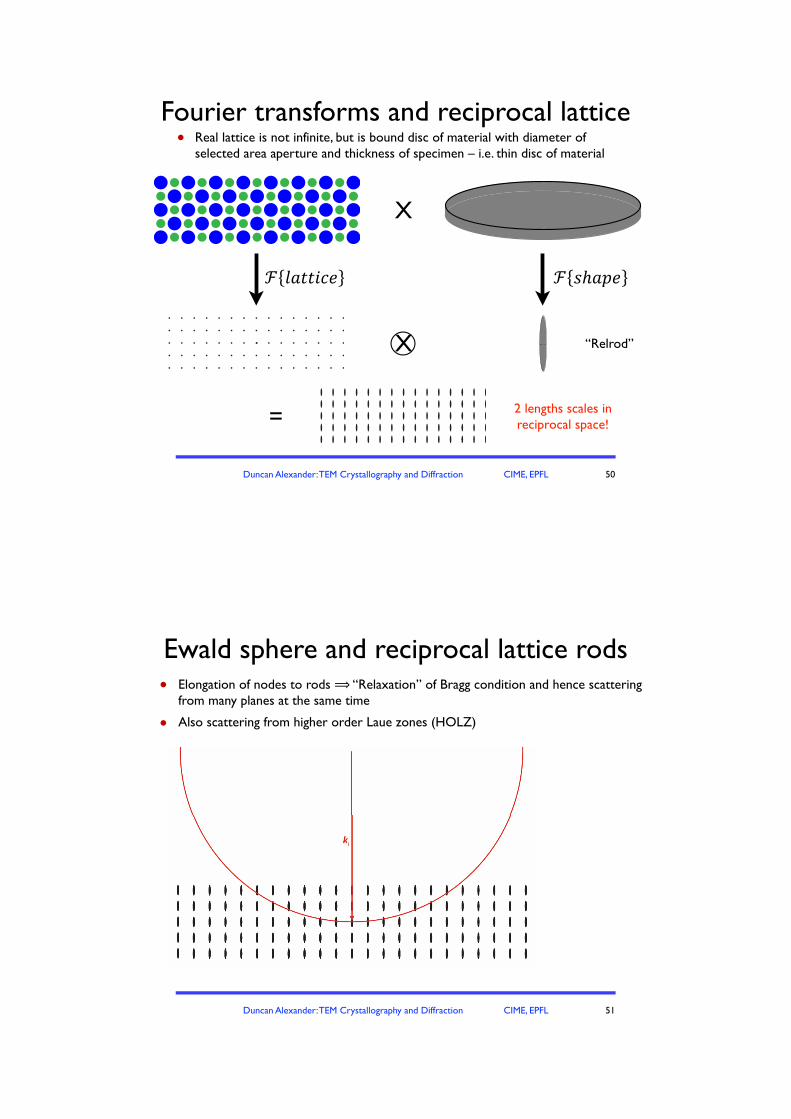
Fourier transforms and reciprocal lattice
50
' Real lattice is not infinite, but is bound disc of material with diameter of!selected area aperture and thickness of specimen – i.e. thin disc of material
Duncan Alexander: TEM Crystallography and Diffraction CIME, EPFL
Ewald sphere and reciprocal lattice rods
51
' Elongation of nodes to rods ! “Relaxation” of Bragg condition and hence scattering from many planes at the same time
' Also scattering from higher order Laue zones (HOLZ)
Duncan Alexander: TEM Crystallography and Diffraction CIME, EPFL
Ewald sphere and reciprocal lattice rods
52
' Elongation of nodes to rods ! “Relaxation” of Bragg condition and hence scattering from many planes at the same time
' Also scattering from higher order Laue zones (HOLZ)
hU + kV + lW = 0hU + kV + lW = 1hU + kV + lW = 2
Zero order Laue zone
First order Laue zone
Second order Laue zone
Duncan Alexander: TEM Crystallography and Diffraction CIME, EPFL
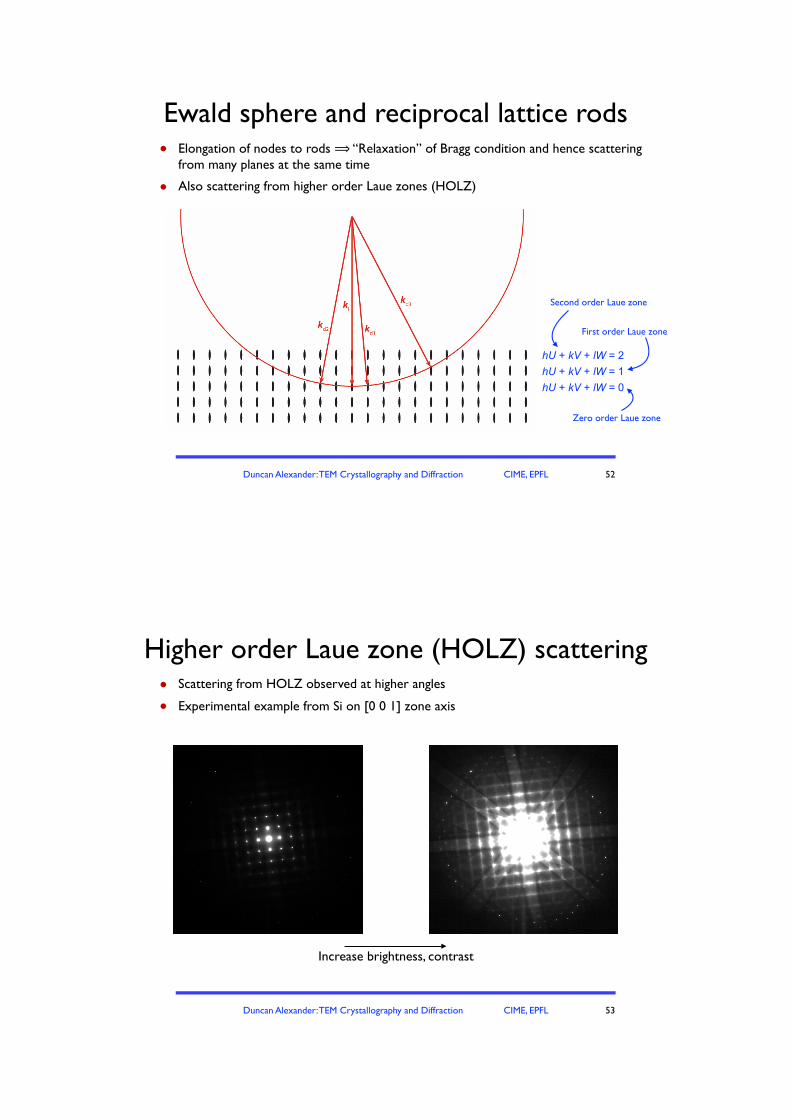
Higher order Laue zone (HOLZ) scattering
53
' Scattering from HOLZ observed at higher angles
' Experimental example from Si on [0 0 1] zone axis
Increase brightness, contrast
Duncan Alexander: TEM Crystallography and Diffraction CIME, EPFL
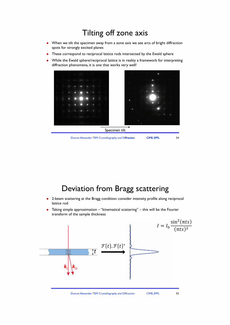
Tilting off zone axis
54
! When we tilt the specimen away from a zone axis we see arcs of bright diffraction spots for strongly excited planes
! These correspond to reciprocal lattice rods intersected by the Ewald sphere
! While the Ewald sphere/reciprocal lattice is in reality a framework for interpreting diffraction phenomena, it is one that works very well!
Specimen tilt
Duncan Alexander: TEM Crystallography and Diffraction CIME, EPFL
Duncan Alexander: TEM Crystallography and Diffraction CIME, EPFL
Deviation from Bragg scattering
55
' 2-beam scattering at the Bragg condition: consider intensity profile along reciprocal lattice rod
' Taking simple approximation – “kinematical scattering” –"this will be the Fourier transform of the sample thickness
kI kD
t
Duncan Alexander: TEM Crystallography and Diffraction CIME, EPFL
Deviation from Bragg scattering
56
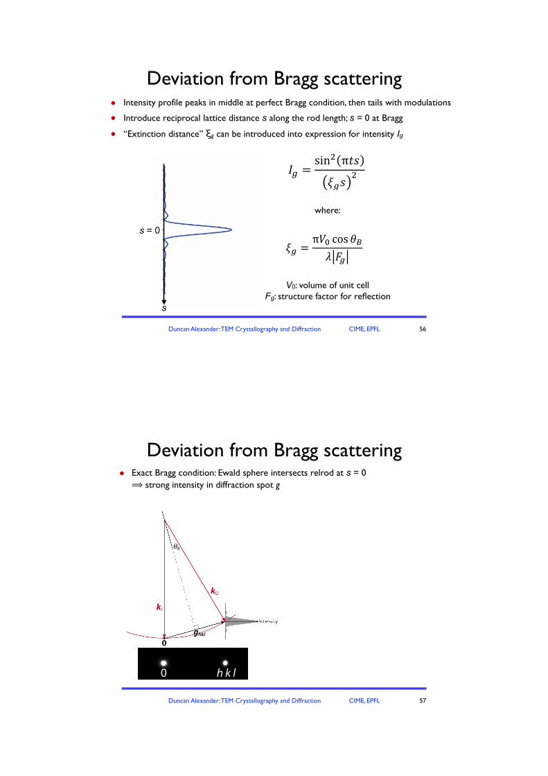
' Intensity profile peaks in middle at perfect Bragg condition, then tails with modulations
' Introduce reciprocal lattice distance s along the rod length; s = 0 at Bragg
' “Extinction distance” (g can be introduced into expression for intensity Ig
s
s = 0
where:
V0: volume of unit cell!Fg: structure factor for reflection
Duncan Alexander: TEM Crystallography and Diffraction CIME, EPFL
Deviation from Bragg scattering
57
' Exact Bragg condition: Ewald sphere intersects relrod at s = 0!! strong intensity in diffraction spot g
h k l0
Duncan Alexander: TEM Crystallography and Diffraction CIME, EPFL
Deviation from Bragg scattering
58
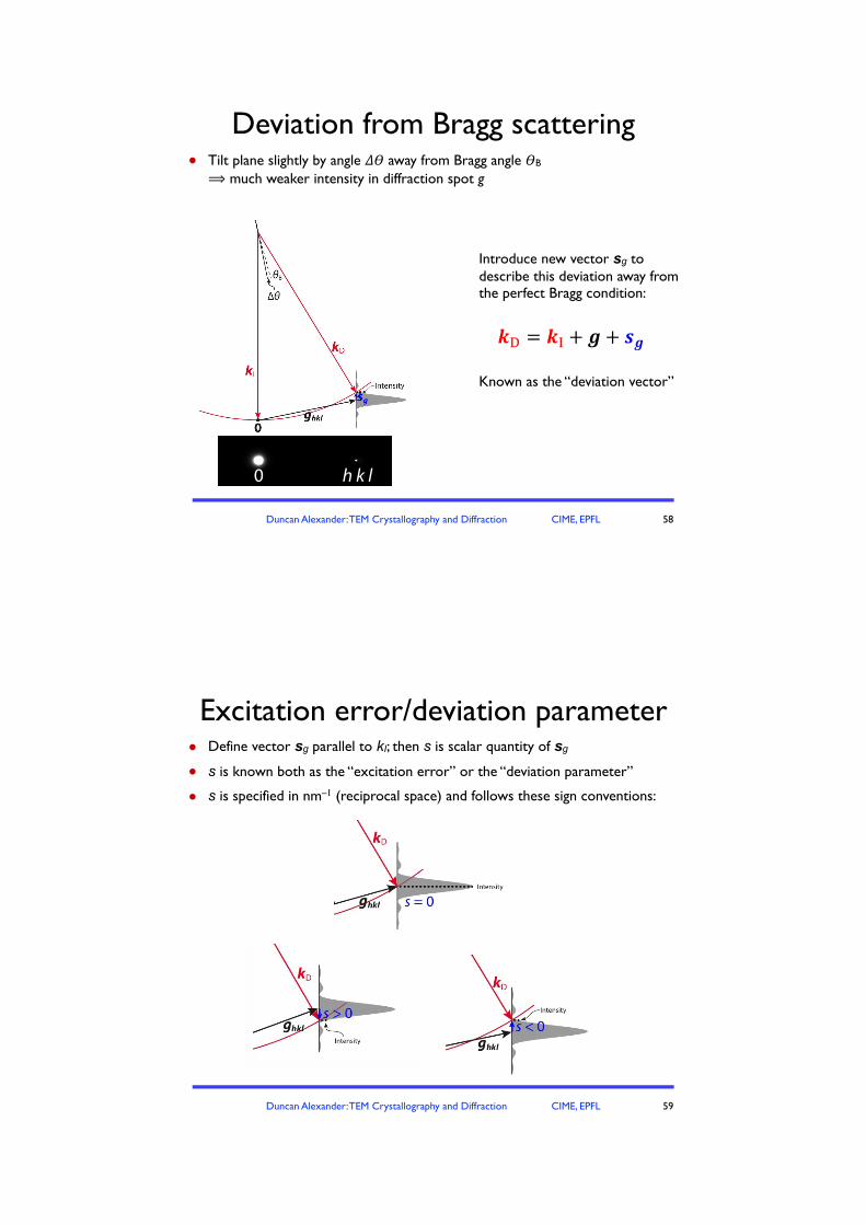
' Tilt plane slightly by angle "# away from Bragg angle #B!! much weaker intensity in diffraction spot g
h k l0
Introduce new vector sg to describe this deviation away from the perfect Bragg condition:
Known as the “deviation vector”
Duncan Alexander: TEM Crystallography and Diffraction CIME, EPFL
Excitation error/deviation parameter
59
' Define vector sg parallel to kI; then s is scalar quantity of sg' s is known both as the “excitation error” or the “deviation parameter”
' s is specified in nm–1 (reciprocal space) and follows these sign conventions:
Duncan Alexander: TEM Crystallography and Diffraction CIME, EPFL
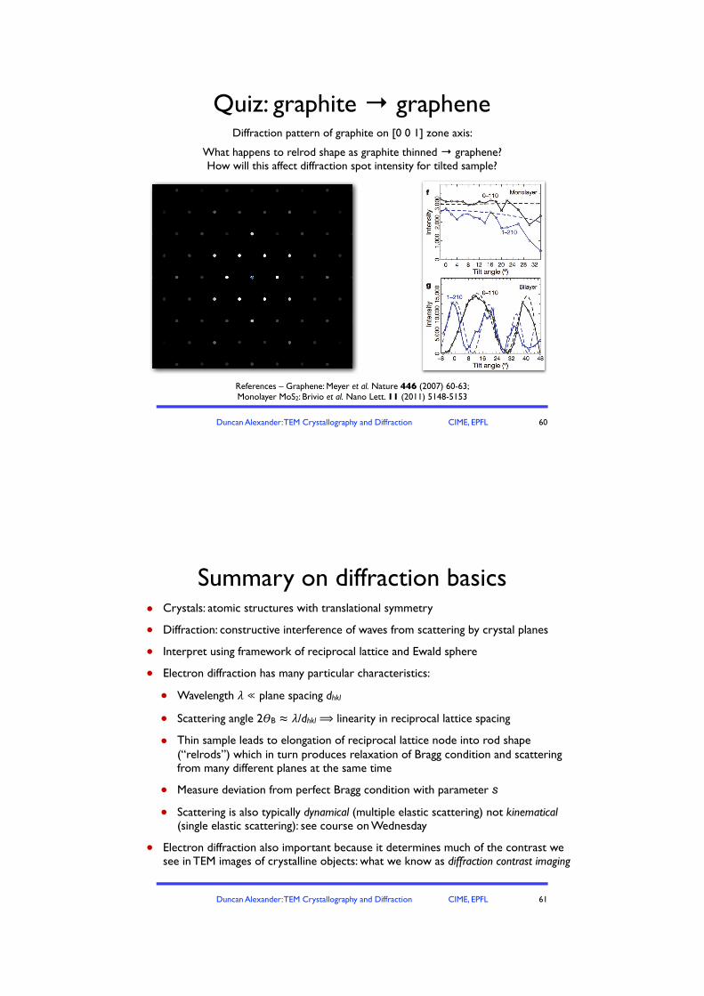
Quiz: graphite ) graphene
60
Diffraction pattern of graphite on [0 0 1] zone axis:
References – Graphene: Meyer et al. Nature 446 (2007) 60-63;Monolayer MoS2: Brivio et al. Nano Lett. 11 (2011) 5148-5153
What happens to relrod shape as graphite thinned ) graphene?How will this affect diffraction spot intensity for tilted sample?
Duncan Alexander: TEM Crystallography and Diffraction CIME, EPFL
Summary on diffraction basics
61
! Crystals: atomic structures with translational symmetry
! Diffraction: constructive interference of waves from scattering by crystal planes
! Interpret using framework of reciprocal lattice and Ewald sphere
! Electron diffraction has many particular characteristics:
! Wavelength ! ! plane spacing dhkl
! Scattering angle 2"B " !/dhkl ! linearity in reciprocal lattice spacing
! Thin sample leads to elongation of reciprocal lattice node into rod shape (“relrods”) which in turn produces relaxation of Bragg condition and scattering from many different planes at the same time
! Measure deviation from perfect Bragg condition with parameter s
! Scattering is also typically dynamical (multiple elastic scattering) not kinematical (single elastic scattering): see course on Wednesday
! Electron diffraction also important because it determines much of the contrast we see in TEM images of crystalline objects: what we know as diffraction contrast imaging