Embed Size (px)
Citation preview
Chapter 2 Scanning probes microscopes
instrumentation
Objective: learn the general techniques that are essential for SPM.
Chapter 2 Scanning probes microscopes
instrumentation
2.1: Tips
STM tips: requirements Geometry: Need for atomically-sharp apex for atomic resolution on a “flat” surface, rest of the tip can be blunt. Strong relief: need for a small angle, otherwise the surface is not faithfully imaged. The latter point is also true for AFM and related techniques.
An artefact: tip imaging
The blunt tip is imaged by the sharp sample needle-like structures.
Effect recognized by observation of numerous identical structures.
Different brightness due to different heights of the needles.
Sample with needle-like structures: a Al2O3 surface imaged by AFM.
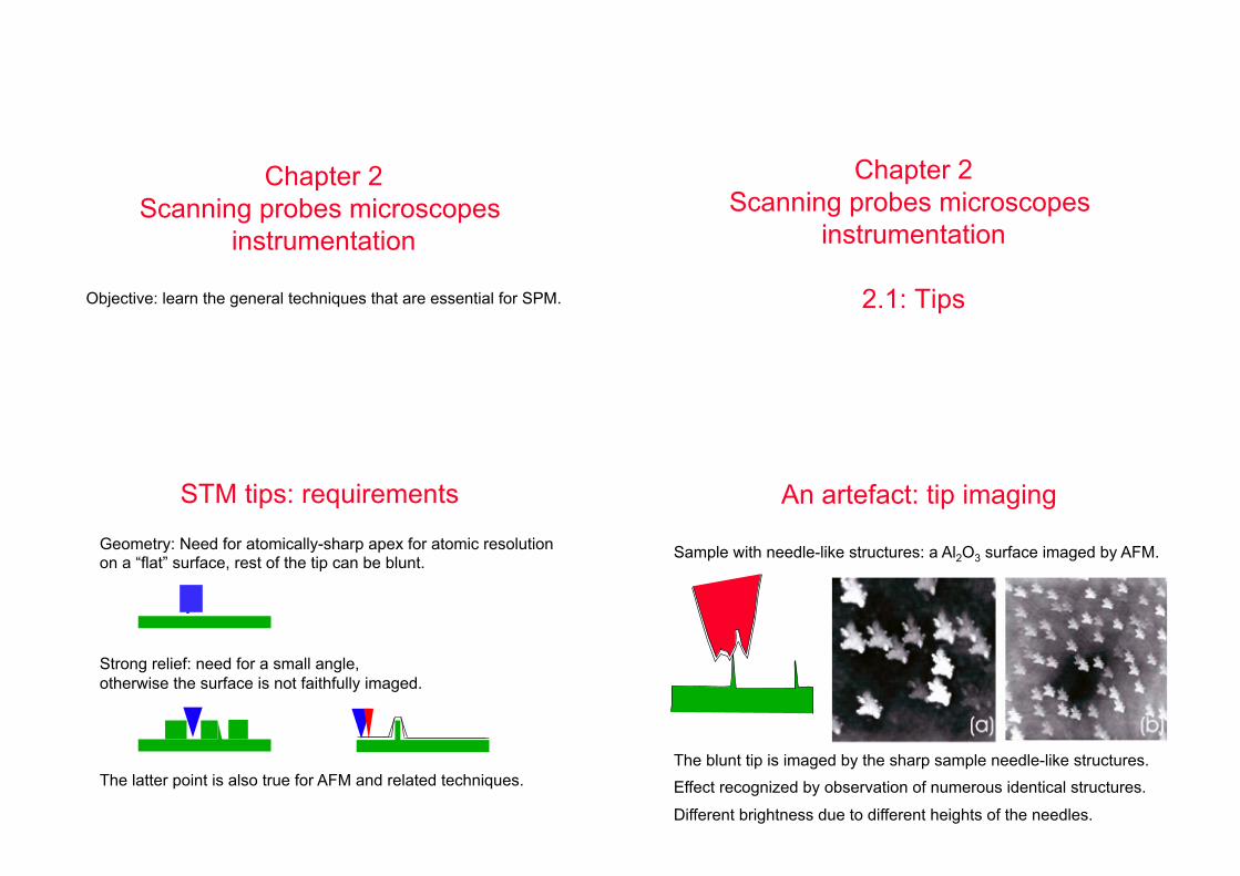
STM tips: materials Criteria: Surface quality, low oxydability, Ease of preparation, Rigidity. Materials: W: easy to etch, rigid. Pt: very low oxydability, but soft. Au: very low oxydability but very soft. Pt90Ir10: good rigidity/oxydability compromise. Tip can be simply cut from a wire. Electrochemistry-based recipies are more reliable.
STM tips: etching techniques
The excess etching time after the drop of the lower part has a strong influence on the final tip geometry: Long over-etch = blunt tip.
Material-dependent, W is easy. The reactants flow governs the locality of the etch.
100 µm
1 µm
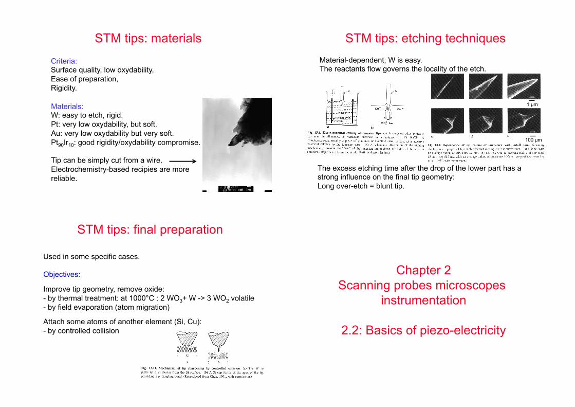
STM tips: final preparation
Used in some specific cases. Objectives:
Improve tip geometry, remove oxide: - by thermal treatment: at 1000°C : 2 WO3+ W -> 3 WO2 volatile - by field evaporation (atom migration)
Attach some atoms of another element (Si, Cu): - by controlled collision
Chapter 2 Scanning probes microscopes
instrumentation
2.2: Basics of piezo-electricity
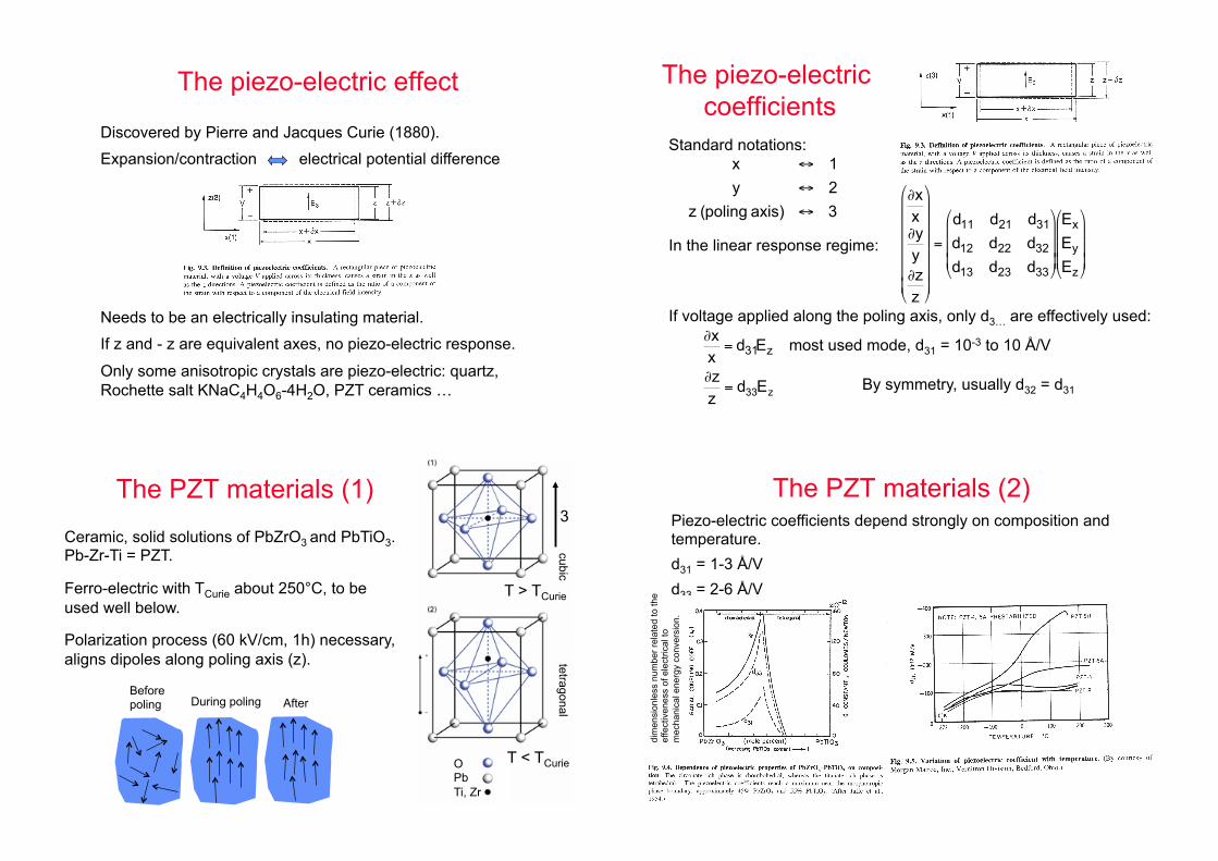
The piezo-electric effect Discovered by Pierre and Jacques Curie (1880).
Expansion/contraction electrical potential difference
Needs to be an electrically insulating material.
If z and - z are equivalent axes, no piezo-electric response.
Only some anisotropic crystals are piezo-electric: quartz, Rochette salt KNaC4H4O6-4H2O, PZT ceramics …
The piezo-electric coefficients
€
x ↔ 1y ↔ 2
z (poling axis) ↔ 3
Standard notations:
€
∂xx∂yy∂zz
#
$
% % % % % %
&
'
( ( ( ( ( (
=
d11 d21 d31
d12 d22 d32
d13 d23 d33
#
$
% % %
&
'
( ( (
Ex
Ey
Ez
#
$
% % %
&
'
( ( (
In the linear response regime:
€
∂xx
= d31Ez
€
∂zz
= d33Ez
most used mode, d31 = 10-3 to 10 Å/V
If voltage applied along the poling axis, only d3… are effectively used:
By symmetry, usually d32 = d31
The PZT materials (1) Ceramic, solid solutions of PbZrO3 and PbTiO3. Pb-Zr-Ti = PZT.
Ferro-electric with TCurie about 250°C, to be used well below.
Polarization process (60 kV/cm, 1h) necessary, aligns dipoles along poling axis (z).
T < TCurie
T > TCurie
3
O Pb Ti, Zr
Before poling During poling After
cubic tetragonal
The PZT materials (2) Piezo-electric coefficients depend strongly on composition and temperature. d31 = 1-3 Å/V d33 = 2-6 Å/V
dim
ensi
onle
ss n
umbe
r rel
ated
to th
e ef
fect
iven
ess
of e
lect
rical
to
mec
hani
cal e
nerg
y co
nver
sion
.
Chapter 2 Scanning probes microscopes
instrumentation
2.3: Piezo-electric actuators
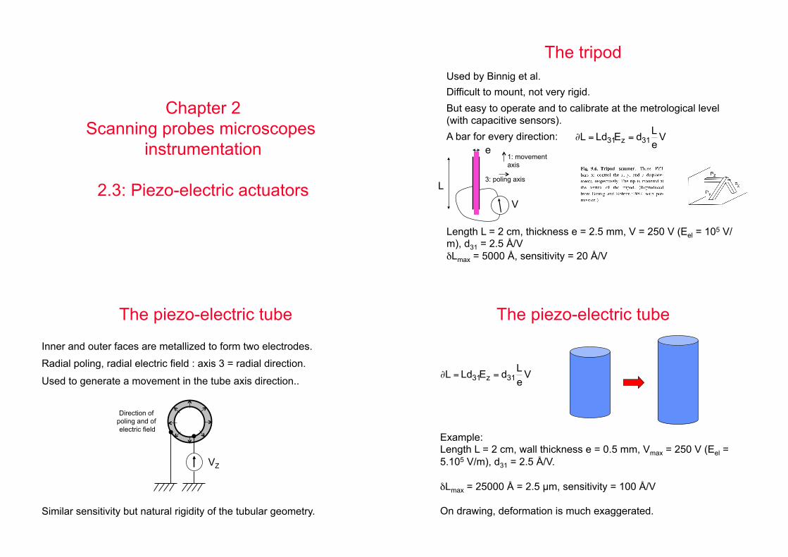
The tripod Used by Binnig et al. Difficult to mount, not very rigid. But easy to operate and to calibrate at the metrological level (with capacitive sensors). A bar for every direction:
V
Length L = 2 cm, thickness e = 2.5 mm, V = 250 V (Eel = 105 V/m), d31 = 2.5 Å/V δLmax = 5000 Å, sensitivity = 20 Å/V
€
∂L = Ld31Ez = d31Le
V
L
e
3: poling axis
1: movement axis
The piezo-electric tube Inner and outer faces are metallized to form two electrodes.
Radial poling, radial electric field : axis 3 = radial direction.
Used to generate a movement in the tube axis direction..
Similar sensitivity but natural rigidity of the tubular geometry.
Direction of poling and of electric field
VZ
The piezo-electric tube
€
∂L = Ld31Ez = d31Le
V
Example: Length L = 2 cm, wall thickness e = 0.5 mm, Vmax = 250 V (Eel = 5.105 V/m), d31 = 2.5 Å/V. δLmax = 25000 Å = 2.5 µm, sensitivity = 100 Å/V On drawing, deformation is much exaggerated.

The scanner tube Tube with again radial poling. Four quadrant electrodes on the outer face: + Vx,y and – Vx,y applied on two opposite electrodes. Again, a voltage Vz can be applied on the (single) internal electrode.
VZ VX -VX VY -VY
The scanner tube
€
∂X =2 2π
d31L2
DeV
Same parameters + Diameter D = 1 cm. δXmax = 50000 Å = 5 µm, sensitivity = 200 Å/V
Bow: displacement not purely lateral. Voltage Vz applied to inner electrode: Z movement capability added. Three movements can be done simultaneously. Compact and quite sensitive : broadly used.
VX -VX
The benders
+V
+V 0
Base
Low stiffness, force and resonant frequency.
A scanner built with 4 benders polarized in two halves: no angle with interest for laser beam reflection in AFM.
Similar effect as the scanner tube but in a single plate geometry.
Poling in the up direction
The shear piezos
€
∂X = d15V
The labels 4, 5 and 6 in piezo-electric coefficients describe rotations. Here, E is applied along direction 1, perpendicular to poling. The corresponding strain coefficient d15 is as high as 11 Å/V.
L = 1 mm, Vmax = 250 V (Eel = 2.5 105 V/m), d15 = 10 Å/V δXmax = 250 Å.
High forces, used in coarse positioning.
V
Chapter 2 Scanning probes microscopes
instrumentation
2.4: Limitations of piezo-electric actuators
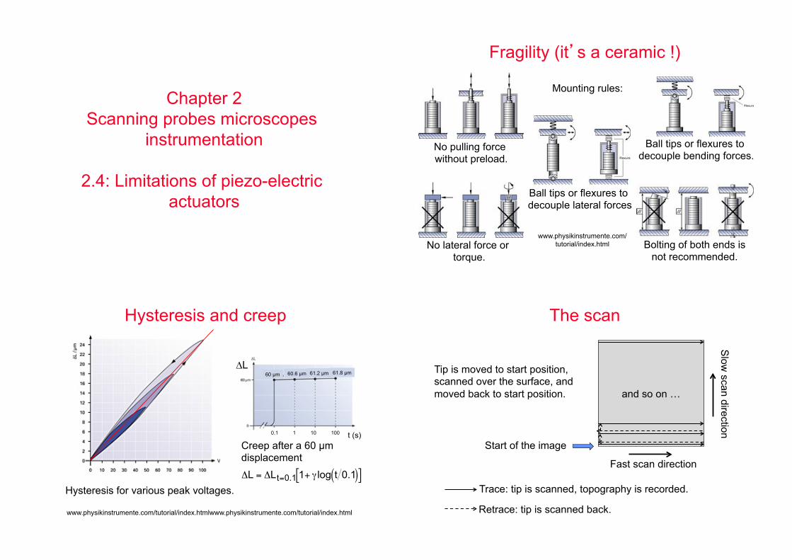
Fragility (it�s a ceramic !)
Mounting rules:
www.physikinstrumente.com/tutorial/index.html Bolting of both ends is
not recommended.
No pulling force without preload.
No lateral force or torque.
Ball tips or flexures to decouple lateral forces
Ball tips or flexures to decouple bending forces.
Hysteresis and creep
Hysteresis for various peak voltages.
Creep after a 60 µm displacement
www.physikinstrumente.com/tutorial/index.htmlwww.physikinstrumente.com/tutorial/index.html
t (s)
61.2 µm 60.6 µm 60 µm 61.8 µm
0.1 1 10 100
∆L
€
ΔL = ΔLt=0.1 1+ γ log t 0.1( )[ ]
The scan
and so on …
Trace: tip is scanned, topography is recorded.
Retrace: tip is scanned back.
Start of the image
Slow
scan direction
Fast scan direction
Tip is moved to start position, scanned over the surface, and moved back to start position.
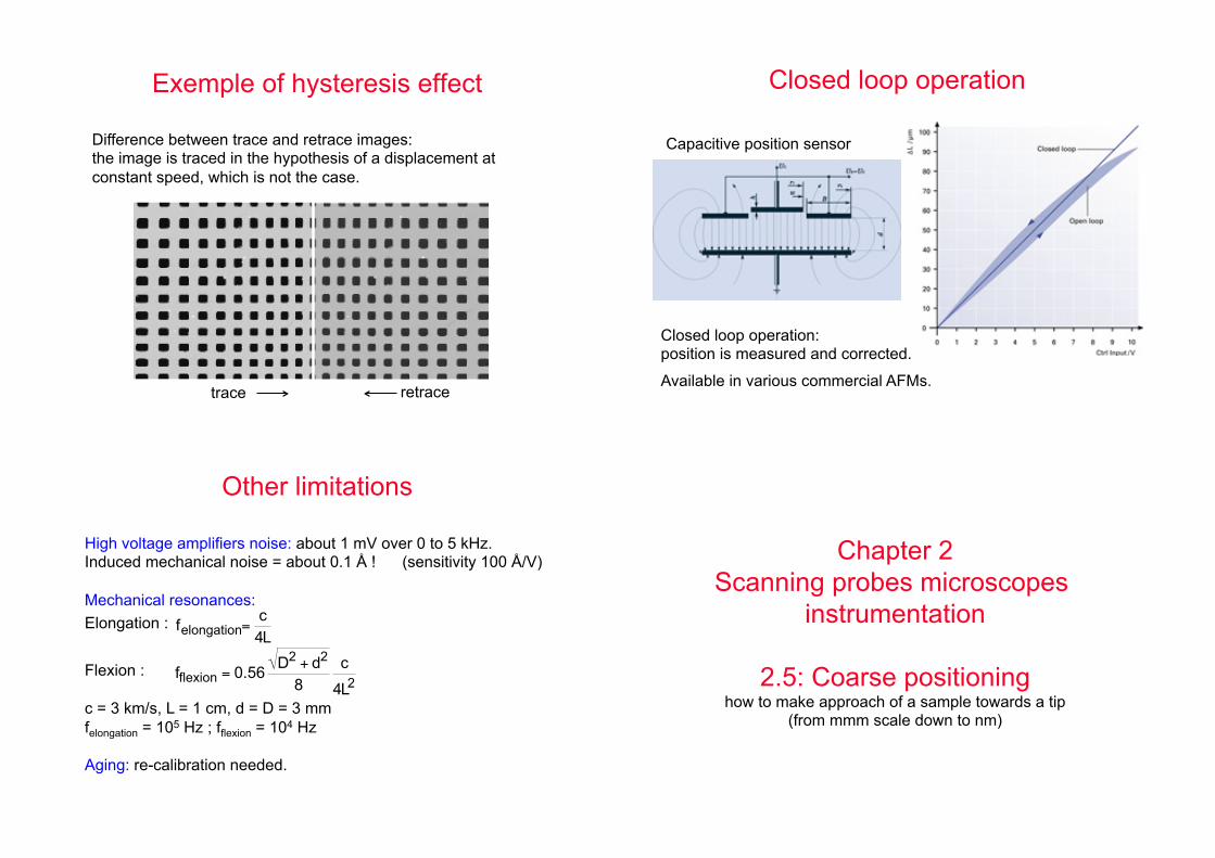
Exemple of hysteresis effect
trace retrace
Difference between trace and retrace images: the image is traced in the hypothesis of a displacement at constant speed, which is not the case.
Closed loop operation
Capacitive position sensor
Closed loop operation: position is measured and corrected.
Available in various commercial AFMs.
Other limitations
High voltage amplifiers noise: about 1 mV over 0 to 5 kHz. Induced mechanical noise = about 0.1 Å ! (sensitivity 100 Å/V) Mechanical resonances: Elongation :
Flexion : c = 3 km/s, L = 1 cm, d = D = 3 mm felongation = 105 Hz ; fflexion = 104 Hz Aging: re-calibration needed.
€
felongation=c4L
€
fflexion = 0.56 D2 + d2
8c
4L2
Chapter 2 Scanning probes microscopes
instrumentation
2.5: Coarse positioning how to make approach of a sample towards a tip
(from mmm scale down to nm)
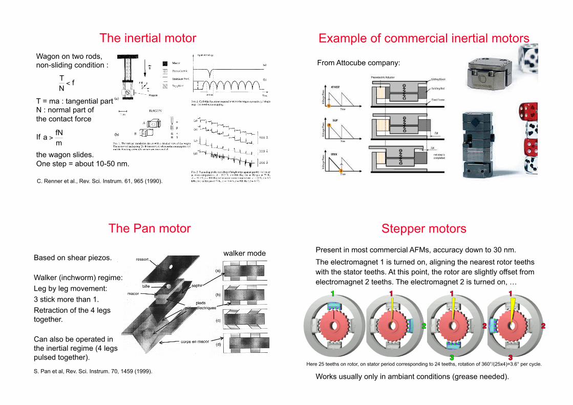
The inertial motor
C. Renner et al., Rev. Sci. Instrum. 61, 965 (1990).
Wagon on two rods, non-sliding condition : T = ma : tangential part N : normal part of the contact force If the wagon slides. One step = about 10-50 nm.
€
TN
< f
€
a >fNm
From Attocube company:
Example of commercial inertial motors
The Pan motor
Based on shear piezos.
Walker (inchworm) regime: Leg by leg movement: 3 stick more than 1. Retraction of the 4 legs together.
Can also be operated in the inertial regime (4 legs pulsed together).
walker mode
S. Pan et al, Rev. Sci. Instrum. 70, 1459 (1999).
Stepper motors Present in most commercial AFMs, accuracy down to 30 nm. The electromagnet 1 is turned on, aligning the nearest rotor teeths with the stator teeths. At this point, the rotor are slightly offset from electromagnet 2 teeths. The electromagnet 2 is turned on, …
Here 25 teeths on rotor, on stator period corresponding to 24 teeths, rotation of 360°/(25x4)=3.6° per cycle.
Works usually only in ambiant conditions (grease needed).

Chapter 2 Scanning probes microscopes
instrumentation
2.6: Design rules and examples
Vibration isolation
Incoming vibrations / mechanical damping. Practical limitation: f0 > 2 Hz
xM = difference between tip and base positions:
Driven harmonic oscillator, ω0, Q.
€
TS =xM0
x0=
ω# ω 0
$
% &
'
( )
2
1− ω# ω 0
$
% &
'
( )
2$
% & &
'
( ) )
2
+ω# Q # ω 0
$
% &
'
( )
2
€
T =x0
xS0=
1+ω
Qω0
#
$ %
&
' (
2
1− ωω0
#
$ %
&
' (
2#
$ % %
&
' ( (
2
+ω
Qω0
#
$ %
&
' (
2
€
xS t( ) = xS0 sin ωt( )
€
x t( ) = x0 sin ωt +ϕ( )
€
xM t( ) = xM0 sin ωt + # ϕ ( )
base
O. Z
üger
, H. P
. Ott,
and
U. D
ürig
, Rev
. Sci
. Ins
trum
. 63,
563
4 (1
992)
.
Driven harmonic oscillator, ω0�, Q�.
Need for a double stage isolation
With a 100 nm vibration source at 1 kHz, a 10-5 transfer amplitude gives here a 1 pm vibration on the microscope. 10-3 gives 100 pm = 1 Å.
With positioning motors
Very low temperature (60 mK) AFM-STM with Attocube motors F. Dahlem, T. Quaglio, H. Courtois (2008).
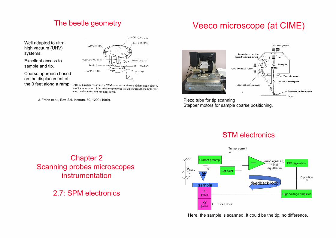
The beetle geometry
Well adapted to ultra-high vacuum (UHV) systems.
Excellent access to sample and tip.
Coarse approach based on the displacement of the 3 feet along a ramp.
J. Frohn et al., Rev. Sci. Instrum. 60, 1200 (1989).
Veeco microscope (at CIME)
Piezo tube for tip scanning Stepper motors for sample coarse positioning.
Chapter 2 Scanning probes microscopes
instrumentation
2.7: SPM electronics
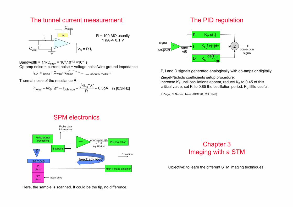
STM electronics
tip
sample Z
piezo
Current preamp.
Set point
PID regulation
Z position
Tunnel current
XY piezo
High Voltage amplifier
Scan drive
Vbias
error signal e(t) = 0 at
equilibrium
feedback loop
Here, the sample is scanned. It could be the tip, no difference.
The tunnel current measurement
R It
VS = R It
Bandwidth = 1/RCstray = 108.10-12 =10-4 s Op-amp noise = current noise + voltage noise/wire-ground impedance Thermal noise of the resistance R :
Cstray
€
iOA = inoise + Cwireωvnoise
R = 100 MΩ usually 1 nA -> 0.1 V
€
Pnoise = 4kBTΔf ⇒ iJohnson =4kBTΔf
R≈ 0.3pA
Cwire
-
+
about 5 nV/Hz1/2
in [0;3kHz]
The PID regulation
correction signal
P
I
D
Σ$error e(t)
signal
set-point
€
KP e t( )
€
KDde t( )
dt
€
KI e t( )dτ∫
P, I and D signals generated analogically with op-amps or digitally.
Ziegel-Nichols coefficients setup procedure: increase KP until oscillations appear, reduce KP to 0.45 of this critical value, set KI to 0.85 the oscillation period. KD little useful.
J. Ziegel, N. Nichols, Trans. ASME 64, 759 (1942).
-
SPM electronics
Z piezo
Set point
PID regulation
XY piezo
High Voltage amplifier
Scan drive
Probe signal processing
Probe data information
Z position
tip
sample feedback loop
Here, the sample is scanned. It could be the tip, no difference.
error signal e(t) = 0 at
equilibrium Chapter 3 Imaging with a STM
Objective: to learn the different STM imaging techniques.
Chapter 3 Imaging with a STM
3.1: Imaging principle and techniques
Important parameters
Voltage bias determines the energy range of probed electronic states
Vtip - Vsample > 0 : e- from sample to tip, occupied states are imaged.
Vtip - Vsample < 0 : e- from tip to sample, empty states are imaged.
Scanning frequency: below the resonance frequency of tubes, below the bandwidth of the tunnel current regulation if active.
Tunnel resistance Rt determines the tip-sample distance. Usually, the current is the parameter:
€
Rt =VIt
= 5 MΩ to 5GΩ
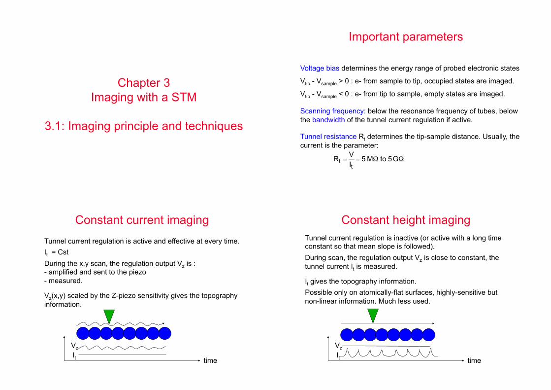
Constant current imaging Tunnel current regulation is active and effective at every time. It = Cst During the x,y scan, the regulation output Vz is : - amplified and sent to the piezo - measured.
Vz(x,y) scaled by the Z-piezo sensitivity gives the topography information.
time
Vz It
Constant height imaging Tunnel current regulation is inactive (or active with a long time constant so that mean slope is followed). During scan, the regulation output Vz is close to constant, the tunnel current It is measured.
It gives the topography information. Possible only on atomically-flat surfaces, highly-sensitive but non-linear information. Much less used.
time
Vz It
Chapter 3 Imaging with a STM
3.2: The spatial resolution
The corrugation Corrugation ∆d is by definition: the topography variation amplitude as measured by the microscope. It is a fraction of Angtröm on an atomically flat surface, and can be larger on rougher surfaces. Depends on every experimental conditions. Can be decreased by a blunt tip, an inefficient regulation …: not an intrinsic quantity.
Spatial resolution
Binnig (1978); hypothesis of a continuous media. The tunnel current is concentrated on a scale: R = 10 nm, α = 1 Å-1 : current flows on a scale ∆x = 1 nm. Spatial resolution is not limited by the tip radius.
Tip radius R
∆x
€
I Δx( ) = I0 exp −αΔx2
R
%
& '
(
) * where α =
2mW
€
Rα
<< R
Trying to model the atomic resolution
€
Δdtheoh
= exp −π2 R + d
αa2
& ' (
) * +
,
- .
/
0 1 if a >>
πα
and d >>2α
,
- .
/
0 1
Stoll (1984)
For a metal : a = 2.5 to 3 Å, k = 1 Å-1, h = 3 Å. Tip: R = d = 3 Å calculated ∆dtheo = 0.01 Å: too small compared to experiment!
Model of a continuous media surface: homogenous electron gas. Calculated corrugation ∆dtheo:
This model fails to describe the atomic resolution: the hypothesis of a continuous media is incorrect.
a ∆d
h d
The origin of atomic resolution
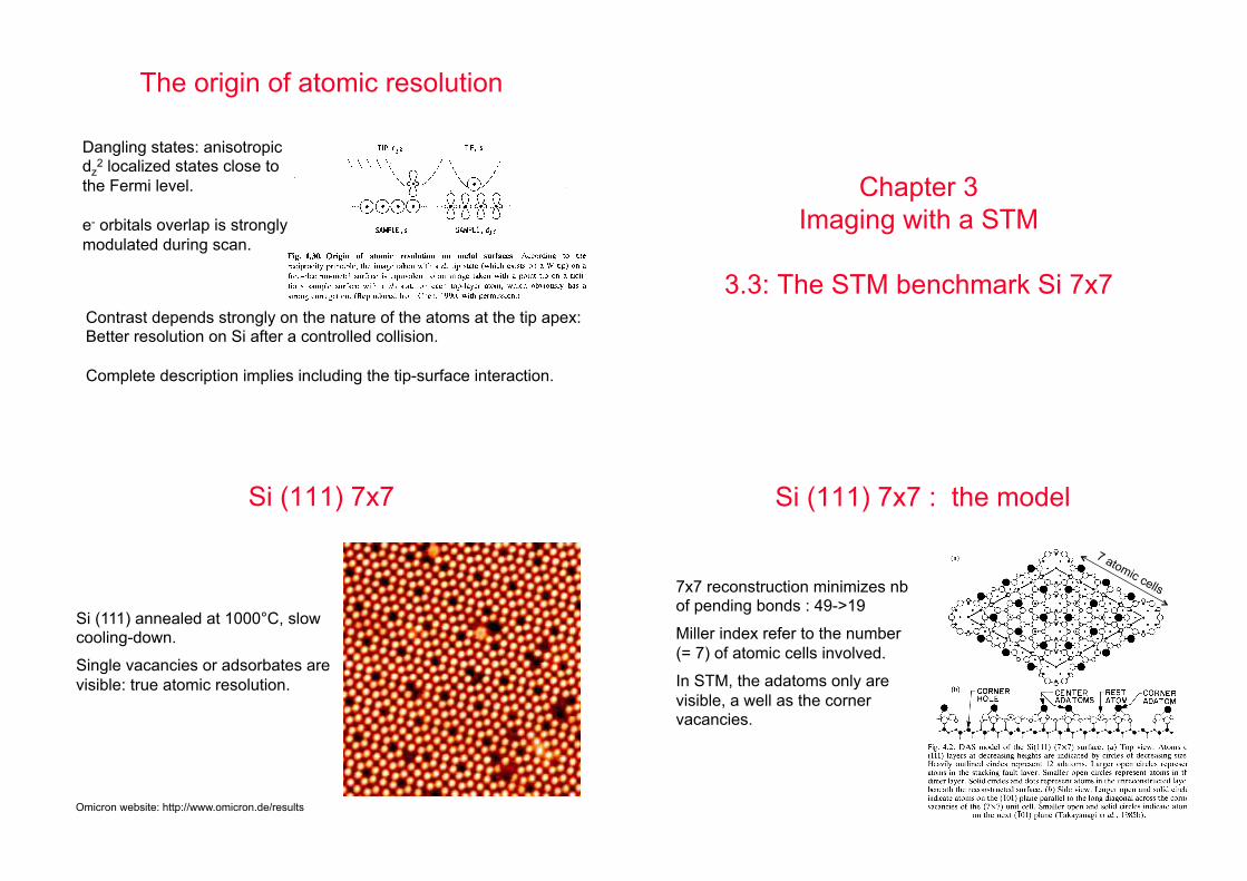
Contrast depends strongly on the nature of the atoms at the tip apex: Better resolution on Si after a controlled collision. Complete description implies including the tip-surface interaction.
Dangling states: anisotropic dz
2 localized states close to the Fermi level. e- orbitals overlap is strongly modulated during scan.
Chapter 3 Imaging with a STM
3.3: The STM benchmark Si 7x7
Si (111) 7x7
Omicron website: http://www.omicron.de/results
Si (111) annealed at 1000°C, slow cooling-down.
Single vacancies or adsorbates are visible: true atomic resolution.
Si (111) 7x7 : the model
7x7 reconstruction minimizes nb of pending bonds : 49->19
Miller index refer to the number (= 7) of atomic cells involved.
In STM, the adatoms only are visible, a well as the corner vacancies.

Surface dynamics studies
Real-time dynamics of Pb atoms on Si
J.-M. Rofriguez-Campos et al, Phys. Rev. Lett. 76, 799 (1996), Institut Néel, Grenoble.