Embed Size (px)
Citation preview

Chapter 1
Infrared DetectorCharacterization
Over the past several hundreds of years, optical systems (telescopes, microscopes,eyeglasses, cameras, etc.) have formed their optical image on the humanretina, photographic plate, or film. The birth of photodetectors dates back to1873 when Smith discovered photoconductivity in selenium. Progress wasslow until 1905, when Einstein explained the newly observed photoelectriceffect in metals, and Planck solved the blackbody emission puzzle byintroducing the quantum hypothesis. Applications and new devices soonflourished, pushed by the dawning technology of vacuum tube sensorsdeveloped in the 1920s and 1930s, culminating in the advent of television.Zworykin and Morton, the celebrated fathers of videonics, on the last page oftheir legendary book Television (1939) concluded that: “when rockets will flyto the moon and to other celestial bodies, the first images we will see of them willbe those taken by camera tubes, which will open to mankind new horizons.”Their foresight became a reality with the Apollo and Explorer missions.Photolithography enabled the fabrication of silicon monolithic imaging focalplanes for the visible spectrum beginning in the early 1960s. Some of theseearly developments were intended for a videophone, and other efforts werefor television cameras, satellite surveillance, and digital imaging. Infraredimaging has been vigorously pursued in parallel with visible imaging becauseof its utility in military applications. More recently (1997), the charged-coupled device (CCD) camera aboard the Hubble Space Telescope delivered adeep-space picture, a result of 10 day’s integration, featuring galaxies ofthe 30th magnitude—an unimaginable figure, even for astronomers of ourgeneration. Thus, photodetectors continue to open to humanity the mostamazing new horizons.
1.1 Introduction
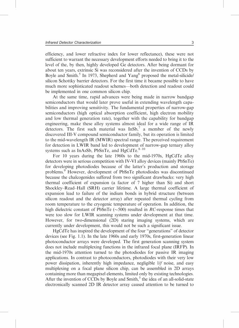
Many materials have been investigated in the infrared (IR) field. Figure 1.1gives approximate dates of significant developmental efforts for infrared
1

materials. During the 1950s, IR detectors were built using single-element-cooled lead salt photodetectors, primarily for anti-air-missile seekers. Usuallylead salt detectors were polycrystalline and were produced by vacuumevaporation and chemical deposition from a solution, followed by a post-growth sensitization process.1 The first extrinsic photoconductive detectorswere reported in the early 1950s2 after the discovery of the transistor, whichstimulated a considerable improvement and growth of material purificationtechniques. Since the techniques for controlled impurity introduction becameavailable for germanium at an earlier date, the first high-performance extrin-sic detectors were based on Ge:Hg with activation energy for the Hg acceptorof 0.089 eV. Extrinsic photoconductive response from copper, zinc, and goldimpurity levels in germanium gave rise to devices using the 8- to 14-mm longwavelength IR (LWIR) spectral window and beyond to the 14- to 30-mm verylong wavelength IR (VLWIR) region.
In 1967 the first comprehensive extrinsic Si detector-oriented paper waspublished by Soref.4 However, the state of extrinsic Si was not changed signi-ficantly. Although Si has several advantages over Ge (namely, a lower dielectricconstant giving shorter dielectric relaxation time and lower capacitance, higherdopant solubility and larger photoionization cross section for higher quantum
Figure 1.1 History of the development of infrared detectors and systems. New concepts ofdetectors developed in last two decades are marked in blue. Four generations of systemscan be considered for principal military and civilian applications: first generation (scanningsystems), second generation (staring systems with electronic scanning), third generation(staring systems with a large number of pixels and two-color functionality), and fourthgeneration (staring systems with a very large number of pixels, multi-color functionality, andother on-chip functions; e.g., better radiation/pixel coupling, avalanche multiplication inpixels, and polarization/phase sensitivity) (adapted from Ref. 3).
2 Chapter 1
efficiency, and lower refractive index for lower reflectance), these were notsufficient to warrant the necessary development efforts needed to bring it to thelevel of the, by then, highly developed Ge detectors. After being dormant forabout ten years, extrinsic Si was reconsidered after the invention of CCDs byBoyle and Smith.5 In 1973, Shepherd and Yang6 proposed the metal-silicide/silicon Schottky barrier detectors. For the first time it became possible to havemuch more sophisticated readout schemes—both detection and readout couldbe implemented in one common silicon chip.
At the same time, rapid advances were being made in narrow bandgapsemiconductors that would later prove useful in extending wavelength capa-bilities and improving sensitivity. The fundamental properties of narrow-gapsemiconductors (high optical absorption coefficient, high electron mobilityand low thermal generation rate), together with the capability for bandgapengineering, make these alloy systems almost ideal for a wide range of IRdetectors. The first such material was InSb,7 a member of the newlydiscovered III-V compound semiconductor family, but its operation is limitedto the mid-wavelength IR (MWIR) spectral range. The perceived requirementfor detection in LWIR band led to development of narrow-gap ternary alloysystems such as InAsSb, PbSnTe, and HgCdTe.8–10
For 10 years during the late 1960s to the mid-1970s, HgCdTe alloydetectors were in serious competition with IV-VI alloy devices (mainly PbSnTe)for developing photodiodes because of the latter’s production and storageproblems.9 However, development of PbSnTe photodiodes was discontinuedbecause the chalcogenides suffered from two significant drawbacks: very highthermal coefficient of expansion (a factor of 7 higher than Si) and shortShockley–Read–Hall (SRH) carrier lifetime. A large thermal coefficient ofexpansion lead to failure of the indium bonds in hybrid structure (betweensilicon readout and the detector array) after repeated thermal cycling fromroom temperature to the cryogenic temperature of operation. In addition, thehigh dielectric constant of PbSnTe (�500) resulted in RC-response times thatwere too slow for LWIR scanning systems under development at that time.However, for two-dimensional (2D) staring imaging systems, which arecurrently under development, this would not be such a significant issue.
HgCdTe has inspired the development of the four “generations” of detectordevices (see Fig. 1.1). In the late 1960s and early 1970s, first-generation linearphotoconductor arrays were developed. The first generation scanning systemdoes not include multiplexing functions in the infrared focal plane (IRFP). Inthe mid-1970s attention turned to the photodiodes for passive IR imagingapplications. In contrast to photoconductors, photodiodes with their very lowpower dissipation, inherently high impedance, negligible 1/f noise, and easymultiplexing on a focal plane silicon chip, can be assembled in 2D arrayscontaining more than megapixel elements, limited only by existing technologies.After the invention of CCDs by Boyle and Smith,5 the idea of an all-solid-stateelectronically scanned 2D IR detector array caused attention to be turned to
3Infrared Detector Characterization

HgCdTe photodiodes. In the end of the 1970s the emphasis was directed towardlarge photovoltaic HgCdTe arrays in the MWIR and LWIR spectral bands forthermal imaging. Recent efforts have been extended to short wavelengths,e.g., for starlight imaging in the short wavelength IR (SWIR) range, as well asto VLWIR spaceborne remote sensing beyond 15 mm.
The third-generation HgCdTe and type-II superlattice (T2SL) systemscontinue to be developed, and concept development towards the so-calledfourth generation systems was also recently initiated. The definition of fourth-generation systems is not well established. These systems provide enhancedcapabilities in terms of greater number of pixels, higher frame rates, and betterthermal resolution, as well as multicolor functionality and other on-chipfunctions. Multicolor capabilities are highly desirable for advanced IR sys-tems. Collection of data in distinct IR spectral bands can discriminate for boththe absolute temperature and the unique signature of objects within the scene.By providing this new dimension of contrast, multiband detection also offersadvanced color processing algorithms to further improve sensitivity comparedto that of single-color devices. It is expected that the functionalities of fourth-generation systems could manifest themselves as spectral, polarization, phase,or dynamic range signatures that could extract more information from a givenscene.11
At the beginning of the 1990s, several national agencies (e.g., in U.S.,Germany, and France) switched their research emphasis to III-V low-dimensional solid materials (quantum wells and superlattices), as an alternativetechnology option to HgCdTe, to attain their stated goal of inexpensive large-area IR focal plane arrays (FPAs) amenable to fabrication by the horizontalintegration of material foundries and processing centers of excellence. There hasbeen considerable progress towards the materials development and device designinnovations. Several new concepts for improvement of the performance of pho-todetectors have been proposed (see bottom part of Fig. 1.1), where approximatedata of significant development efforts are marked in blue. In particular,significant advances have been made in the bandgap engineering of variouscompound III-V semiconductors that has led to new detector architectures.New emerging strategies include T2SLs, barrier structures such as nBn detectorswith lower generation–recombination leakage mechanisms, photon trappingdetectors, and multi-stage/cascade infrared devices. The barrier-structure detec-tor concept has recently been applied to resurrect the performance of III-VFPAs, allowing them to operate at considerably higher temperatures than theirphotodiode counterparts simply by the elimination of depletion regions in theabsorber volume. At present, the trade-offs between both competing III-Vand II-VI IR materials technologies is observed. It is expected that these twosignificant schools of thought with regard to the ultimate in photon detection,namely, operation at room temperature, might play a crucial role in the futuredevelopments.
4 Chapter 1

1.2 Classification of Infrared Detectors
Optical radiation is considered to be radiation ranging from vacuum ultravioletto submillimeter wavelengths (25 nm to 3000 mm). The terahertz (THz) regionof electromagnetic spectrum (see Fig. 1.2) is often described as the finalunexplored area of the spectrum and still presents a challenge for both elec-tronic and photonic technologies. It is frequently treated as the spectralregion within the frequency range of n� 0.1–10 THz (l� 3 mm – 30 mm)and is partly overlapping with the loosely treated submillimeter (sub-mm)wavelength band n� 0.1–3 THz (l� 3 mm – 100 mm).
The majority of optical detectors can be classified in two broad categories:photon detectors (also called quantum detectors) and thermal detectors.
1.2.1 Photon detectors
In photon detectors the radiation is absorbed within the material by interactionwith electrons either bound to lattice atoms or to impurity atoms or with freeelectrons. The observed electrical output signal results from the changedelectronic energy distribution. The fundamental optical excitation processes insemiconductors are illustrated in Fig. 1.3. In quantum wells [Fig. 1.3(b)] theintersubband absorption takes place between the energy levels of a quantum wellassociated with the conduction band (n-doped) or valence band (p-doped). In thecase of type-II InAs/GaSb superlattice [Fig. 1.3(c)] the superlattice bandgap isdetermined by the energy difference between the electron miniband E1 andthe first heavy-hole state HH1 at the Brillouin zone center. A consequence of thetype-II band alignment is spatial separation of electrons and holes.
Relative response of infrared detectors is plotted as a function of wave-length with either a vertical scale of W–1 or photon–1 (see Fig. 1.4). The
Figure 1.2 The electromagnetic spectrum (adapted from Ref. 12).
5Infrared Detector Characterization

photon detectors show a selective wavelength dependence of response perunit incident radiation power. Their response is proportional to the rate ofarrival photons as the energy per photon is inversely proportional to wave-length. In consequence, the spectral response increases linearly with increasingwavelength [see Fig. 1.4(a)], until the cutoff wavelength is reached, which isdetermined by the detector material. The cutoff wavelength is usuallyspecified as the long wavelength point at which the detector responsivity fallsto 50% of the peak responsivity.
Thermal detectors tend to be spectrally flat in the first case (their response isproportional to the energy absorbed), thus they exhibit a flat spectral response[see Fig 1.4(a)], while photon detectors are generally flat in the second case[see Fig. 1.4(b)].
Photon detectors exhibit both good signal-to-noise performance and avery fast response. But to achieve this, the photon IR detectors may requirecryogenic cooling. This is necessary to prevent the thermal generation ofcharge carriers. The thermal transitions compete with the optical ones,making non-cooled devices very noisy.
Figure 1.3 Optical excitation processes in: (a) bulk semiconductors, (b) quantum wells,and (c) type-II InAs/GaSb superlattices.
Figure 1.4 Relative spectral response for a photon and thermal detector for (a) constantincident radiant power and (b) photon flux, respectively.
6 Chapter 1
Depending on the nature of the interaction, the class of photon detectorsis further sub-divided into different types. The most important are: intrinsicdetectors, extrinsic detectors, and photoemissive detectors (Schottky bar-riers).3 Different types of detectors are briefly characterized in Table 1.1.
A key difference between intrinsic and extrinsic detectors is that extrinsicdetectors require much cooling to achieve high sensitivity at a given spectralresponse cutoff in comparison with intrinsic detectors. Low-temperatureoperation is associated with longer-wavelength sensitivity in order to suppressnoise due to thermally induced transitions between close-lying energy levels.
There is a fundamental relationship between the temperature of thebackground viewed by the detector and the lower temperature at which thedetector must operate to achieve background-limited performance (BLIP).HgCdTe photodetectors with a cutoff wavelength of 12.4 mm operate at77 K. One can scale the results of this example to other temperatures andcutoff wavelengths by noting that for a given level of detector performance,Tlc� constant;13 i.e., the longer lc, the lower is T while their product remainsroughly constant. This relation holds because quantities that determinedetector performance vary mainly as an exponential of Eexc/kT ¼ hc/kTlc,where Eexc is the excitation energy, k is Boltzmann’s constant, h is Planck’sconstant, and c is the velocity of light.
The long wavelength cutoff can be approximated as
Tmax ¼300Klc½mm� : (1.1)
The general trend is illustrated in Fig. 1.5 for six high-performancedetector materials suitable for low-background applications: Si, InGaAs,InSb, HgCdTe photodiodes, and Si:As blocked impurity band (BIB)detectors; and extrinsic Ge:Ga unstressed and stressed detectors. Terahertzphotoconductors are operated in extrinsic mode.
The most widely used photovoltaic detector is the p–n junction, where astrong internal electric field exists across the junction even in the absence ofradiation. Photons incident on the junction produce free hole–electron pairsthat are separated by the internal electric field across the junction, causing achange in voltage across the open-circuit cell or a current to flow in the short-circuited case. Due to the absence of recombination noise, the limiting p–njunction’s noise level can ideally be
p2 times lower than that of the
photoconductor.Photoconductors that utilize excitation of an electron from the valence
to conduction band are called intrinsic detectors. Instead those that operate byexciting electrons into the conduction band or holes into the valence bandfrom impurity states within the band (impurity-bound states in energy gap,quantum wells, or quantum dots), are called extrinsic detectors. A key
7Infrared Detector Characterization

Tab
le1.1
Pho
tonde
tectors.
Modeof
operation
Schematic
ofdetector
Operatio
nandpropertie
s
Pho
tocond
uctor
Thisisessentially
aradiation-sensitiveresistor,g
enerally
asemicon
ductor,eitherin
thin
film
orbu
lkform
.A
photon
may
releasean
electron
–ho
lepa
iror
anim
purity-bou
ndcharge
carrier,
therebyincreasing
theelectrical
cond
uctivity.In
almostallcasesthechan
gein
cond
uctivity
ismeasuredby
means
ofelectrod
esattached
tothesample.
For
low-resistancematerial,the
photocon
ductor
isusua
llyop
erated
inaconstant
currentcircuit.For
high
-resistance
photocon
ductors,aconstant
voltagecircuitispreferred,
andthesign
alisdetected
asachan
gein
currentin
thebias
circuit.
Blocked
impu
rity
band
(BIB
)detector
The
active
region
ofaBIB
detector
structure,
usua
llyba
sedon
epitaxially
grow
nn-type
material,issand
wichedbetw
eenahigh
er-dop
eddegenerate
substrateelectrod
ean
dan
undo
ped
blocking
layer.Dop
ingof
theactive
layerishigh
enou
ghfortheon
setof
anim
purity
band
inorderto
displayahigh
quan
tum
efficiency
forim
purity
ionization
(inthecase
ofSi:A
sBIB
,the
active
layerisdo
pedto
�5�10
17cm
–3 ).The
device
exhibits
adiod
e-lik
echaracteristic,except
that
photoexcitationof
electron
stakesplacebetw
eenthedo
norim
purity
andthecond
uction
band
.The
heavily
dopedn-type
IR-activelayerha
sasm
allcon
centration
ofnegatively
charged
compensatingacceptor
impu
rities.Intheab
senceof
anap
pliedbias,c
hargeneutralityrequ
ires
anequa
lconcentrationof
ionizeddo
nors.Whereas
thenegative
chargesarefixedat
acceptor
sites,thepo
sitive
chargesassociated
withionizeddo
norsites(D
þcharges)aremob
ilean
dcan
prop
agatethroug
htheIR
-activelayerviathemecha
nism
ofho
ppingbetw
eenoccupied
(D0 )
andvacant
(Dþ)neighb
oringsites.A
positive
bias
tothetran
sparentcontactcreatesafieldthat
drives
thepre-existing
Dþ
chargestowards
thesubstrate,
while
theun
dopedblocking
layer
preventstheinjectionof
newD
þcharges.A
region
depleted
ofD
þchargesisthereforecreated,
withawidth
depend
ingon
theap
pliedbias
andon
thecompensatingacceptor
concentration.
p–njunction
photod
iode
This
isthemostwidelyused
photov
oltaic
detector
butis
rather
rarely
used
asaTHz
detector.Pho
tons
withen
ergy
greaterthan
theen
ergy
gapcreate
electron
–ho
lepa
irsin
the
materialo
nbo
thside
sof
thejunc
tion
.Bydiffusion,
theelectron
san
dho
lesgene
ratedwithin
adiffusionleng
thfrom
thejunc
tion
reachthespace-ch
arge
region
whe
rethey
aresepa
rated
bythestrong
electric
field;
minoritycarriers
beco
memajoritycarriers
ontheothe
rside
.Thisway
aph
otoc
urrent
isgene
ratedcausingach
ange
invo
ltag
eacross
theop
en-circu
itcell
oracu
rren
tto
flow
intheshort-circuitedcase.The
limitingno
iselevelof
photod
iode
scan
ideallybe
p 2times
lower
than
that
oftheph
otoc
ondu
ctor,du
eto
theab
senc
eof
reco
mbinationno
ise.
Respo
nsetimes
aregene
rallylimited
byde
vice
capa
citanc
ean
dde
tector-circu
itresistan
ce.
8 Chapter 1

nBndetector
The
nBndetector
consistsof
ana
rrow
-gap
n-type
absorber
layer(A
L),athin
wide-gapba
rrier
layer(BL),an
dana
rrow
-gap
n-type
contactlayer(C
L).The
thin
wide-gapBLpresentsalarge
barrierin
thecond
uction
band
that
elim
inates
electron
flow
.Current
throug
hthenB
ndetector
relieson
tran
sportof
mob
ileho
lesthroug
hdriftan
ddiffusionin
theBLbetw
eenthetw
on-type
narrow
-gap
region
s.Effectively,thenB
ndetector
isdesign
edto
redu
cetheda
rkcurrent
(generation–
recombina
tion
currentoriginatingwithinthedepletionlayer)
andno
isewitho
utim
peding
theph
otocurrent
(signa
l).In
particular,theba
rrierserves
toredu
cethesurface
leak
agecurrent.The
nBndetector
operates
asaun
ipolar
unity-gain
detector,an
dthisdesign
canbe
stated
asahy
brid
betw
eenph
otocon
ductor
andph
otod
iode.
Metal-insulator-
semicon
ductor
(MIS)ph
otod
iode
The
MIS
device
consistsof
ametal
gatesepa
ratedfrom
asemicon
ductor
surfaceby
aninsulator
(I).Byap
plying
anegative
voltageto
themetal
electrod
e,electron
sarerepelledfrom
theI–S
interface,
creating
adepletionregion
.Whenincident
photon
screate
hole–electron
pairs,the
minoritycarriers
driftaw
ayto
thedepletionregion
andthevo
lumeof
thedepletionregion
shrink
s.The
totala
mou
ntof
charge
that
aph
otog
atecancollect
isdefinedas
itswellcap
acity.
The
totalwellcapa
city
isdecidedby
thegate
bias,theinsulatorthickn
ess,thearea
ofthe
electrod
es,a
ndtheba
ckgrou
nddo
ping
ofthesemicon
ductor.N
umerou
ssuch
photog
ates
with
prop
erclocking
sequ
ence
form
aCCD
imagingarray.
Scho
ttky
barrier
photod
iode
Scho
ttky
barrierph
otod
iodesreveal
somead
vantages
over
p–njunction
photod
iodes:
fabricationsimplicity(depositionof
metal
barrieron
n(p)-sem
icon
ductor),ab
senceof
high
-temperature
diffusionprocesses,an
dhigh
speedof
respon
se.S
ince
itisamajoritycarrierdevice,
minoritycarrierstoragean
dremov
alprob
lemsdo
notexist,an
dthereforehigh
erba
ndwidths
canbe
expected.
The
thermionicem
ission
processin
aScho
ttky
barrierismuchmoreefficientthan
thediffusion
process,an
dthereforeforagivenbu
ilt-invo
ltage,thesaturation
currentin
aScho
ttky
diod
eis
severalorders
ofmagnitude
high
erthan
inthep–
njunction
.
9Infrared Detector Characterization

difference between intrinsic and extrinsic detectors is that extrinsic detectorsrequire much cooling to achieve high sensitivity at a given spectral responsecutoff in comparison with intrinsic detectors. Low-temperature operation isassociated with longer-wavelength sensitivity in order to suppress noise due tothermally induced transitions between close-lying energy levels. Intrinsicdetectors are most common at the short wavelengths, below 20 mm. In thelonger-wavelength region the photoconductors are operated in extrinsic mode.One advantage of photoconductors is their current gain, which is equal to therecombination time divided by the majority-carrier transit time. This currentgain leads to higher responsivity than is possible with nonavalanching pho-tovoltaic detectors. However, serious problem of photoconductors operated atlow temperature is nonuniformity of detector element due to recombinationmechanisms at the electrical contacts and its dependence on electrical bias.
Recently, interfacial workfunction internal photoemission detectors, quan-tum well and quantum dot detectors, which can be included to extrinsic photo-conductors, have been proposed especially for IR and THz spectral bands.3 Thevery fast time response of quantum well and quantum dot semiconductordetectors make them attractive for heterodyne detection.
1.2.2 Thermal detectors
The second class of detectors is composed of thermal detectors. In a thermaldetector shown schematically in Fig. 1.6, the incident radiation is absorbed to
Figure 1.5 Operating temperatures for low-background material systems with theirspectral band of greatest sensitivity. The dashed line indicates the trend toward loweroperating temperature for longer-wavelength detection (adapted from Ref. 3).
10 Chapter 1

change the material temperature, and the resultant change in some physicalproperty is used to generate an electrical output. The detector is suspended onlags, which are connected to the heat sink. The signal does not depend uponthe photonic nature of the incident radiation. Thus, thermal effects aregenerally wavelength independent [see Fig. 1.4(a)]; the signal depends uponthe radiant power (or its rate of change) but not upon its spectral content.Since the radiation can be absorbed in a black surface coating, the spectralresponse can be very broad. Attention is directed toward three approachesthat have found the greatest utility in infrared technology, namely, bolo-meters, pyroelectric, and thermoelectric effects. The thermopile is one of theoldest IR detectors, and is a collection of thermocouples connected in series inorder to achieve better temperature sensitivity. In pyroelectric detectors achange in the internal electrical polarization is measured, whereas in the caseof thermistor bolometers a change in the electrical resistance is measured. Fora long time, thermopiles were slow, insensitive, bulky, and costly devices. Butwith developments in semiconductor technology, thermopiles can be opti-mized for specific applications. Recently, thanks to conventional complemen-tary metal-oxide semiconductor (CMOS) processes, the thermopile’s on-chipcircuitry technology has opened the door to mass production.
Usually a bolometer is a thin, blackened flake or slab, whose impedance ishighly temperature dependent. Bolometers may be divided into several types.The most commonly used are the metal, the thermistor, and the semiconduc-tor bolometers. A fourth type is the superconducting bolometer. This bolo-meter operates on a conductivity transition in which the resistance changes
Figure 1.6 Schematic diagram of thermal detector (adapted from Ref. 3).
11Infrared Detector Characterization

dramatically over the transition temperature range. Figure 1.7 showsschematically the temperature dependence of resistance of different types ofbolometers.
Many types of thermal detectors are operated in wide spectral range ofelectromagnetic radiation. The operation principles of thermal detectors arebriefly described in Table 1.2.
Microbolometer detectors are now produced in larger volumes than allother IR array technologies together. At present, VOx microbolometer arraysare clearly the most used technology for uncooled detectors. VOx wins thebattle between the amorphous silicon bolometers and barium strontiumtitanate (BST) ferroelectric detectors.
1.3 Detector Figures of Merit
It is difficult to measure the performance characteristics of infrared detectorsbecause of the large number of experimental variables involved. A variety ofenvironmental, electrical, and radiometric parameters must be taken intoaccount and carefully controlled. With the advent of large 2D detector arrays,detector testing has become even more complex and demanding.
This section is intended to serve as an introductory reference for thetesting of infrared detectors. Numerous texts and journals cover this issue,including: Infrared System Engineering14 by R. D. Hudson; The InfraredHandbook,15 edited by W. L. Wolfe and G. J. Zissis; The Infrared and Electro-Optical Systems Handbook,16 edited by W. D. Rogatto; and Fundamentals ofInfrared Detector Operation and Testing17 by J. D. Vincent, and secondedition of Vincent’s book.18 In this chapter we have restricted our consid-eration to detectors whose output consists of an electrical signal that isproportional to the radiant signal power.
Figure 1.7 Temperature dependence of resistance of three bolometer material types.
12 Chapter 1

Tab
le1.2
The
rmal
detectors.
Modeof
operation
Schematic
ofdetector
Operatio
nandpropertie
s
Therm
opile
The
thermocou
pleisusua
llyathin,blackenedflak
econn
ectedthermally
tothejunction
oftw
odissim
ilarmetalsor
semicon
ductors.Heatab
sorbed
bytheflak
ecauses
atemperature
rise
ofthe
junction
,an
dhenceathermoelectricelectrom
otiveforceisdevelopedthat
canbe
measured.
Altho
ughthermop
ilesareno
tas
sensitiveas
bolometersan
dpy
roelectric
detectors,they
will
replacethesein
man
yap
plications
dueto
theirrelia
blecharacteristicsan
dgo
odcost/perform
ance
ratio.
Therm
ocou
ples
arewidelyused
inspectroscopy
.
Bolom
eter
Metal
Semicon
ductor
Supercon
ductor
Hot
electron
The
bolometer
isaresistiveelem
entconstructedfrom
amaterialwith
avery
smallthermal
capacity
andlargetemperature
coefficient
sothat
theabsorbed
radiationprod
uces
alargechan
gein
resistan
ce.
The
change
inresistance
islik
eto
theph
otocon
ductor,ho
wever,thebasicdetectionmechanism
isdifferent.In
thecase
ofabo
lometer,radiant
power
prod
uces
heat
with
inthematerial,which
inturn
prod
uces
theresistance
change.There
isno
direct
photon
-electroninteraction.
Initially,m
ostb
olom
eterswerethethermistortype
madefrom
oxides
ofmanganese,cob
alt,or
nickel.
Atpresent,microbo
lometersarefabricated
inlarge-form
atarrays
forthermal
imagingap
plications.
Someextrem
elysensitive
low-tem
perature
semicon
ductor
andsupercon
ductor
bolometersareused
intheTHzregion
.
Pyroelectric
detector
The
pyroelectric
detector
canbe
considered
asasm
allcapa
citorwithtw
ocond
ucting
electrod
esmou
nted
perpendicularlyto
thedirectionof
spon
taneou
spo
larization
.Duringincident
ofradiation,
thechan
gein
polarization
appearsas
acharge
onthecapa
citoran
dacurrentis
generated,
themagnitude
ofwhich
depend
son
thetemperature
rise
andthepy
roelectrical
coefficientof
thematerial.The
sign
al,ho
wever,mustbe
chop
pedor
mod
ulated.The
detector
sensitivityislim
ited
either
byam
plifierno
iseor
byloss-tan
gent
noise.
Respo
nsespeedcanbe
engineered
mak
ingpy
roelectric
detectorsuseful
forfast
laserpu
lsedetection,
however
with
prop
ortion
aldecrease
insensitivity.
Golay
cell
The
Golay
cellconsists
ofan
herm
etically
sealed
containerfilledwithgas(usually
xeno
nforits
low
thermal
cond
uctivity)an
darrang
edso
that
expa
nsionof
thegasun
derheatingby
aph
oton
sign
aldistortsaflexiblemem
bran
eon
which
amirrorismou
nted.T
hemov
ementof
themirroris
used
todeflectabeam
oflig
htshiningon
aph
otocella
ndso
prod
ucingachan
gein
theph
otocell
currentas
theou
tput.Inmod
ernGolay
cells
theph
otocellisreplaced
byasolid
-state
photod
iode
andlig
ht-emitting
diod
eisused
forillum
ination.
The
performan
ceof
theGolay
cellison
lylim
ited
bythetemperature
noiseassociated
withthe
thermal
exchan
gebetw
eentheab
sorbingfilm
andthedetector
gas,consequently
thedetector
can
beextrem
elysensitivewithD
*�3�10
9cm
Hz1
/2W
–1 ,an
drespon
sivities
of10
5to
106V/W
.The
respon
setimeisqu
itelong
,typically
15msec.
13Infrared Detector Characterization

1.3.1 Responsivity
The responsivity of an infrared detector is defined as the ratio of the rootmean square (rms) value of the fundamental component of the electricaloutput signal of the detector to the rms value of the fundamental componentof the input radiation power. The units of responsivity are volts per watt(V/W) or amperes per watt (amp/W).
The voltage (or analogous current) spectral responsivity is given by
Rvðl, f Þ ¼Vs
FeðlÞ, (1.2)
where Vs is the signal voltage due to Fe, and Fe(l) is the spectral radiantincident power (in W).
An alternative to the above monochromatic quality, the blackbodyresponsivity, is defined by the equation
RvðT , f Þ ¼ Vs
∫`0 FeðlÞdl, (1.3)
where the incident radiant power is the integral over all wavelengths of thespectral density of power distribution Fe(l) from a blackbody. The respon-sivity is usually a function of the bias voltage, the operating electrical fre-quency, and the wavelength.
1.3.2 Noise equivalent power
The noise equivalent power (NEP) is the incident power on the detectorgenerating a signal output equal to the rms noise output. Stated another way,the NEP is the signal level that produces a signal-to-noise ratio (SNR) of 1. Itcan be written in terms of responsivity:
NEP ¼ Vn
Rv¼ In
Ri: (1.4)
The unit of NEP is watts.The NEP is also quoted for a fixed reference bandwidth, which is often
assumed to be 1 Hz. This “NEP per unit bandwidth” has a unit of watts persquare root hertz (W/Hz1/2).
1.3.3 Detectivity
The detectivity D is the reciprocal of NEP:
D ¼ 1NEP
: (1.5)
14 Chapter 1
It was found by Jones19 that for many detectors the NEP is proportionalto the square root of the detector signal that is proportional to the detectorarea Ad. This means that both NEP and detectivity are functions of electricalbandwidth and detector area, so a normalized detectivity D� (or D-star)suggested by Jones19,20 is defined as
D� ¼ DðAdDf Þ1∕2 ¼ðAdDf Þ1∕2NEP
: (1.6)
The importance of D� is that this figure of merit permits comparison ofdetectors of the same type, but having different areas. Either a spectral orblackbody D� can be defined in terms of the corresponding type of NEP.
Useful equivalent expressions to Eq. (1.6) include:
D� ¼ DðAdDf Þ1∕2Vn
Rv ¼DðAdDf Þ1∕2
InRi ¼
DðAdDf Þ1∕2Fe
ðSNRÞ, (1.7)
where D� is defined as the rms SNR in a 1-Hz bandwidth per unit rmsincident radiant power per square root of detector area. D� is expressed inunits of cm Hz1/2W–1, which recently has been referred to as “Jones.”
Spectral detectivity curves for a number of commercially available IRdetectors are shown in Fig. 1.8. Interest has focused mainly on the twoatmospheric windows 3–5 mm (MWIR) and 8–14 mm (LWIR) (atmospherictransmission is the highest in these bands and the emissivity maximum of theobjects at T� 300 K is at the wavelength l� 10 mm), although in recent yearsthere has been increasing interest in longer wavelengths stimulated by spaceapplications. The spectral character of the background is influenced by thetransmission of the atmosphere that controls the spectral ranges of the infraredfor which the detector may be used when operating in the atmosphere.
1.3.4 Quantum efficiency
A signal whose photon energy is sufficient to generate photocarriers willcontinuously lose energy as the optical field propagates through the semi-conductor. Inside the semiconductor, the field decays exponentially as energyis transferred to the photocarriers. The material can be characterized by anabsorption length a and a penetration depth 1/a. Penetration depth is thepoint at which 1/e of the optical signal power remains.
The power absorbed in the semiconductor as a function of position withinthe material is then
Pa ¼ Pið1� rÞð1� e�axÞ: (1.8)
The number of photons absorbed is the power (in watts) divided by thephoton energy (E ¼ hv). If each absorbed photon generates a photocarrier,
15Infrared Detector Characterization

the number of photocarriers generated per number of incident photons for aspecific semiconductor with reflectivity r is given by
hðxÞ ¼ ð1� rÞð1� e�axÞ, (1.9)
where 0≤ h≤ 1 is a definition for the detector’s quantum efficiency as thenumber of electron–hole pairs generated per incident photon.
Figure 1.9 shows the quantum efficiency of some of the detector materialsused to fabricate arrays of ultraviolet (UV), visible, and infrared detectors.Photocathodes and AlGaN detectors are being developed in the UV region.Silicon p-i-n diodes are shown with and without antireflection coating. Leadsalts (PbS and PbSe) have intermediate quantum efficiencies, while PtSiSchottky barrier types and quantum well infrared photodetectors (QWIPs)have low values. InSb can respond from the near UV out to 5.5 mm at 80 K. Asuitable detector material for the near-IR (1.0–1.7 mm) spectral range isInGaAs lattice matched to the InP. Various HgCdTe alloys, in bothphotovoltaic and photoconductive configurations, cover from 0.7 mm to over20 mm. InAs/GaSb strained layer superlattices have emerged as an alternative
Figure 1.8 Comparison of the D of various commercially available infrared detectors whenoperated at the indicated temperature. The chopping frequency is 1000 Hz for all detectorsexcept the thermopile (10 Hz), thermocouple (10 Hz), thermistor bolometer (10 Hz), Golaycell (10 Hz), and pyroelectric detector (10 Hz). Each detector is assumed to view ahemispherical surround at a temperature of 300 K. Theoretical curves for the background-limited D for ideal photovoltaic and photoconductive detectors and thermal detectors arealso shown (adapted from Ref. 3).
16 Chapter 1

to the HgCdTe. Impurity-doped (Sb, As, and Ga) silicon BIB detectorsoperating at 10 K have a spectral response cutoff in the range of 16– to 30– mm.Impurity-doped Ge detectors can extend the response out to 100–200 mm.
1.4 Fundamental Detector Performance Limits
In general, the detector can be considered as a slab of homogeneoussemiconductor with actual “electrical” area Ae, thickness t, and volume Aet(see Fig. 1.10). Usually, the optical and electrical areas of the device are thesame or similar. However, the use of some kind of optical concentrator canincrease the Ao/Ae ratio by a large factor.
Figure 1.9 Quantum efficiency of different detectors.
Figure 1.10 Model of a photodetector (adapted from Ref. 3).
17Infrared Detector Characterization

The detectivity D� of an infrared photodetector is limited by generationand recombination rates G and R (in m–6s–1) in the active region of thedevice.21 It can be expressed as
D� ¼ l
21=2hcðG þ RÞ1=2�Ao
Ae
�h
t1=2, (1.10)
where l is the wavelength, h is Planck’s constant, c is the velocity of light, andh is the quantum efficiency.
For a given wavelength and operating temperature, the highest perfor-mance can be obtained by maximizing the ratio of the quantum efficiency tothe square root of the sum of the sheet thermal generation and recombinationrates h/[(GþR)t]1/2. This means that high quantum efficiency must beobtained with a thin device.
A possible way to improve the performance of IR detectors is to reducethe physical volume of the semiconductor, thus reducing the amount ofthermal generation. However, this must be achieved without decrease inquantum efficiency, optical area, and field of view (FOV) of the detector.
At equilibrium, the generation and recombination rates are equal. If wefurther assume Ae ¼ Ao, the detectivity of an optimized infrared photodetec-tor is limited by thermal processes in the active region of the device. It can beexpressed as
D� ¼ 0.31l
hck�a
G
�1=2, (1.11)
where 1≤ k≤ 2 and is dependent on the contribution of recombination andbackside reflection. The k-coefficient can be modified by using moresophisticated coupling of the detector with IR radiation, e.g., using photoniccrystals or surface plasmon-polaritons.
The ratio of the absorption coefficient to the thermal generation rate, a/G,is the fundamental figure of merit of any material intended for infraredphotodetection. The a/G ratio versus temperature for various material systemscapable of bandgap tuning is shown in Fig. 1.11 for a hypothetical energygap equal to 0.25 eV (l¼ 5 mm) [Fig. 1.11(a)] and 0.124 eV (l ¼ 10 mm)[Fig. 1.11(b)]. Procedures used in calculations of a/G for different materialsystems are given in Ref. 22. Analysis shows that narrow-gap semiconductorsare more suitable for high-temperature photodetectors in comparison tocompeting technologies such as extrinsic devices, QWIP (quantum well IRphotodetector) and QDIP (quantum dot IR photodetector) devices. The mainreason for the high performance of intrinsic photodetectors is the high densityof states in the valence and conduction bands, which results in strong absorp-tion of infrared radiation. Figure 1.11(b) predicts that a recently emerging
18 Chapter 1

competing IR material, type-II superlattice, is the most efficient materialtechnology for IR detection in the long-wavelength region, theoreticallyperhaps even better than HgCdTe if the influence of the Shockley–Read–Halllifetime is not considered. It is characterized by a high absorption coefficientand relatively low fundamental (band-to-band) thermal generation rate.However, this theoretical prediction has not been confirmed by experimentaldata. It is also worth noting that theoretically AlGaAs/GaAs QWIP is also abetter material than extrinsic silicon.
The ultimate performance of infrared detectors is reached when the detectorand amplifier noise are low compared to the photon noise. The photon noise isfundamental in the sense that it arises not from any imperfection in the detectoror its associated electronics but rather from the detection process itself, as aresult of the discrete nature of the radiation field. The radiation falling on thedetector is a composite of that from the target and that from the background.The practical operating limit for most infrared detectors is not the signalfluctuation limit but the background fluctuation limit, also known as thebackground-limited infrared photodetector (BLIP) limit.
The expression for shot noise can be used to derive the BLIP detectivity,
D�BLIPðl,TÞ ¼ l
hck�
h
2FB
�1=2, (1.12)
where h is the quantum efficiency, and FB is the total background photon fluxdensity reaching the detector, denoted as
Figure 1.11 a/G ratio versus temperature for (a) MWIR (l¼5 mm) and (b) LWIR(l¼ 10 mm) photodetectors based on HgCdTe, QWIP, Si extrinsic, and type-II superlattice(for LWIR only) material technology (adapted from Ref. 3).
19Infrared Detector Characterization

FB ¼ sin2ðu=2Þ∫lc
0Fðl,TBÞdl, (1.13)
where u is the detector field of view angle.Planck’s photon emittance (in units of photons cm–2s–1 mm–1) at
temperature TB is given by
Fðl,TBÞ ¼2pc
l4½expðhc=lkTBÞ � 1� ¼1.885� 1023
l4½expð14.388=lkTBÞ � 1� : (1.14)
Equation (1.12) holds for photovoltaic detectors, which are shot-noiselimited. Photoconductive detectors that are generation-recombination noiselimited have a lower D�
BLIP by a factor of 21/2:
D�BLIPðl, f Þ ¼
l
2 hck�
h
FB
�1=2: (1.15)
Once background-limited performance is reached, quantum efficiency h isthe only detector parameter that can influence detector’s performance.
Figure 1.12 shows the peak spectral detectivity of a background-limitedphotodetector operating at 300, 230, and 200 K, versus the wavelengthcalculated for 300 K background radiation and hemispherical FOV(u ¼ 90 deg). The minimum D�
BLIP (300 K) occurs at 14 mm and equals4.6 � 1010 cm Hz1/2/W. For some photodetectors that operate at near
Figure 1.12 Calculated spectral detectivities of a photodetector limited by the hemispheri-cal FOV background radiation of 300 K as a function of the peak wavelength for detectoroperating temperatures of 300, 230, and 200 K (reprinted from Ref. 23).
20 Chapter 1

equilibrium conditions, such as non-sweep-out photoconductors, the recom-bination rate is equal to the generation rate. For these detectors thecontribution of recombination to the noise will reduce D�
BLIP by a factor of21/2. Note that D�
BLIP does not depend on area and the Ao/Ae ratio. As aconsequence, the background-limited performance cannot be improved bymaking Ao/Ae large.
The highest performance possible will be obtained by the ideal detectorwith unity quantum efficiency and ideal spectral responsivity [R(l) increaseswith wavelength to the cutoff wavelength lc at which the responsivity drops tozero]. This limiting performance is of interest for comparison with actualdetectors.
The detectivity of BLIP detectors can be improved by reducing the back-ground photon flux FB. Practically, there are two ways to do this: a cooled orreflective spectral filter to limit the spectral band or a cooled shield to limit theangular field of view of the detector (as described above). The formereliminates background radiation from spectral regions in which the detectorneed not respond. The best detectors yield background-limited detectivities inquite narrow fields of view.
1.5 Performance of Focal Plane Arrays
This section discusses concepts associated with the performance of focal planearrays (FPAs). For arrays the relevant figure of merit for determining theultimate performance is not the detectivity D�, but the noise equivalentdifference temperature (NEDT) and the modulation transfer function (MTF).NEDT and MTF are considered as the primary performance metrics tothermal imaging systems: thermal sensitivity and spatial resolution. Thermalsensitivity is concerned with the minimum temperature difference that can bediscerned above the noise level. The MTF concerns the spatial resolution andanswers the question of how small an object can be and still be imaged by thesystem. The general approach of system performance is given by Lloyd in hisfundamental monograph.24
1.5.1 Modulation transfer function
The modulation transfer function (MTF) expresses the ability of an imagingsystem to faithfully image a given object; it quantifies the ability of the systemto resolve or transfer spatial frequencies.25 Consider a bar pattern with across-section of each bar being a sine wave. Since the image of a sine wavelight distribution is always a sine wave, the image is always a sine waveindependent of the other effects in the imaging system, such as aberrations.
Usually, imaging systems have no difficulty in reproducing the bar patternwhen the bar pattern is sparsely spaced. However, an imaging system reaches
21Infrared Detector Characterization

its limit when the features of the bar pattern get closer and closer together.When the imaging system reaches this limit, the contrast or the modulation Mis defined as
M ¼ Emax � Emin
Emax þ Emin, (1.16)
where E is the irradiance. Once the modulation of an image is measuredexperimentally, the MTF of the imaging system can be calculated for thatspatial frequency using
MTF ¼ M image
Mobject: (1.17)
The system MTF is dominated by the optics, detector, and display MTFsand can be cascaded by simply multiplying the MTF components to obtainthe MTF of the combination. In spatial frequency terms, the MTF of animaging system at a particular operating wavelength is dominated by limits setby the size of the detector and the aperture of the optics. More details aboutthis issue is given in section 9.2.
1.5.2 Noise equivalent difference temperature
Noise equivalent difference temperature (NEDT) is a figure of merit for ther-mal imagers that is commonly reported. In spite of its widespread use in infra-red literature, it is applied to different systems, in different conditions, andwith different meanings.26
NEDT of a detector represents the temperature change, for incident radia-tion, that gives an output signal equal to the rms noise level. While normallythought of as a system parameter, detector NEDT and system NEDT are thesame except for system losses. NEDT is defined as
NEDT ¼ VnðT∕FÞðVs∕FÞ ¼ Vn
DTDVs
, (1.18)
where Vn is the rms noise, F is the spectral photon flux density (photons/cm2s)incident on a focal plane, and DVs is the signal measured for the temperaturedifference DT.
We follow Kinch27 further to obtain useful equations for noise equivalentirradiance (NEI) and NEDT, used for estimation of detector performance(see e.g., section 6.6).
In modern IR FPAs the current generated in a biased photon detector isintegrated onto a capacitive node with a carrier well capacity of Nw. For anideal system, in absence of excess noise, the detection limit of the node is
22 Chapter 1

achieved when a minimum detectable signal flux DF creates a signal equalshot noise on the node:
DFhAdtint ¼ffiffiffiffiffiffiffiNw
p¼
ffiffiffiffiffiffiffiffiffiffiffiffiffiffiffiffiffiffiffiffiffiffiffiffiffiffiffiffiffiffiffiffiffiffiffiffiffiðJdark þ JFÞAdtint
q
s, (1.19)
where h is the detector collection efficiency, Ad is the detector area, tint is theintegration time, Jdark is the detector dark current, and JF is the flux current.
Associated with NEDT is the other critical parameter, the so-called noiseequivalent flux (NEDF). This parameter is defined for spectral regions inwhich the thermal background flux does not dominate. By equating theminimum detectable signal to the integrated current noise, we have
hFsAdtint ¼ffiffiffiffiffiffiffiffiffiffiffiffiffiffiffiffiffiffiffiffiffiffiffiffiffiffiffiffiffiffiffiffiffiffiffiffiffiðJdark þ JFÞAdtint
q
s, (1.20)
giving
NEDF ¼ 1h
ffiffiffiffiffiffiffiffiffiffiffiffiffiffiffiffiffiffiffiffiffiffiJdark þ JF
qAdtint
s: (1.21)
This can be converted to a noise equivalent irradiance (NEI), which isdefined as the minimum observable flux power incident on the systemaperture, by renormalizing the incident flux density on the detector to thesystem aperture area Aopt. The NEI is given by
NEI ¼ NEDFAdhnAopt
, (1.22)
where monochromatic radiation of energy hn is assumed.NEI [photons/(cm2sec)] is the signal flux level at which the signal produces
the same output as the noise present in the detector. This unit is useful becauseit directly gives the photon flux above which the detector will be photon-noiselimited.
For high-background-flux conditions, the signal flux can be defined asDF ¼ DT(dFB/dT). Thus, for shot noise, substituting in Eq. (1.19), we have
hDTdFB
dT¼
ffiffiffiffiffiffiffiffiffiffiffiffiffiffiffiffiffiffiffiffiffiffiJdark þ JF
qAdtint
s: (1.23)
Finally, after some re-arrangement,
23Infrared Detector Characterization

NEDT ¼ 1þ ðJdark∕JFÞffiffiffiffiffiffiffiffiffiffiffiNwC
p , (1.24)
where C ¼ (dFB/dT)/FB is the scene contrast through the optics. In derivingEq. (1.24) it was assumed that the optics transmission is unity, and that thecold shield of the detector is not contributing flux. This is reasonable at lowdetector temperatures but not at higher operating temperatures. At highertemperatures the scene contrast is defined in terms of the signal flux comingthrough the optics, whereas the flux current is defined by the total fluxthrough the optics and the flux from the cold shield.
1.5.3 Other issues
Infrared photodetectors are typically operated at cryogenic temperatures todecrease the noise of the detector arising from various mechanisms associatedwith the narrow bandgap. There are considerable efforts to decrease systemcost, size, weight, and power consumption, to increase the operating tempera-ture in so-called high-operating-temperature (HOT) detectors. Increasing theoperating temperature of the detector reduces the cooling load, allowing morecompact cooling systems with higher efficiency. Because the cost of the opticsmade from Ge (the standard material for IR optics) rises approximately withthe square of the lens diameter, the reduction of the pixel size results in asignificantly reduced cost of the optics. In addition, the reduction in pixel sizeallows for a larger number of FPAs to be fabricated on each wafer.
Pixel reduction is also needed to increase the detection and identificationrange of infrared imaging systems. It appears that, e.g., the detection range ofmany uncooled IR imaging systems is limited by pixel resolution rather thansensitivity. Figure 1.13 presents a trade-off analysis of the detection range and
Figure 1.13 Calculated detection range as a function of sensor optics for increasingdetector pixel size and format using NVESD NVTherm IP modeling, assuming a 35-mKNEDT (F/1, 30Hz) for all detectors (reprinted from Ref. 28).
24 Chapter 1

sensor optics for a thermal weapon sight using the NVESD NVTherm IPmodel, assuming a detector sensitivity of 35-mK NETD (F/1, 30 Hz) for the25-, 17-, and 12-mm pitch pixel of uncooled FPAs. The advantages of smallpixel pitch and large-format FPAs are obvious. By switching to smaller pitchand larger format detectors, the detection range of a weapon sight increasessignificantly with a fixed optical entrance aperture.
Key challenges in realizing ultimate pixel dimensions in FPA design includ-ing dark current, pixel hybridization, pixel delineation, and unit cell readoutcapacity are considered in Refs. 27 and 29, and Section 9.2 of this book.
It is interesting to consider the performance requirements of near-room-temperature photodetectors for thermal cameras. It can be shown3 that thethermal resolution of infrared thermal systems is characterized by theequation
NEDT ¼ 4ðF=#Þ2Df 1=2A1=2
d topt
24 ∫lb
la
dMdT
D�ðlÞdl35, (1.25)
where F/# is the optics f-number, Df is the frequency band, Ad is the detectorarea, topt is the optics transmission, and M is the spectral emittance of theblackbody described by Planck’s law.
As Eq. (1.25) shows, the thermal resolution improves with an increase indetector area. However, increasing detector area results in reduced spatialresolution. Hence, a reasonable compromise between the requirement of highthermal resolution and spatial resolution is necessary. Improvement ofthermal resolution without detrimental effects on spatial resolution may beachieved by:
• an decrease of detector area combined with a corresponding decrease ofthe optics f-number,
• improved detector performance, and• an increase in the number of detectors.
As was mentioned before, increasing the aperture is undesirable because itincreases the size, mass, and price of an IR system. It is more appropriate touse a detector with higher detectivity. This can be achieved by better couplingof the detector with the incident radiation. Another possibility is theapplication of a multi-elemental sensor, which reduces each elementbandwidth proportionally to the number of elements for the same frame rateand other parameters.
Figure 1.14 shows the dependence of detectivity on the cutoff wavelengthfor a photodetector thermal imager with a resolution of 0.1 K. Detectivities of1.9 � 108 cm Hz1/2/W, 2.3 � 108 cm Hz1/2/W, and 2 � 109 cm Hz1/2/W arenecessary to obtain NEDT ¼ 0.1 K for 10-mm, 9-mm, and 5-mm cutoffwavelengths, respectively. The above estimations indicate that the ultimate
25Infrared Detector Characterization

performance of the uncooled photodetectors is not sufficient to achieve athermal resolution of 0.1 K. Thermal resolution below 0.1 K is achieved forstaring thermal imagers containing thermal FPAs.
The previous considerations are valid assuming that the temporal noiseof the detector is the main source of noise. However, this assertion is not truefor staring arrays, where the nonuniformity of the detector response is a signi-ficant source of noise. This nonuniformity appears as a fixed-pattern noise(spatial noise) and is defined in various ways in the literature. The mostcommon definition is that it is the dark signal nonuniformity arising from anelectronic source (i.e., other than thermal generation of the dark current);e.g., clock breakthrough or from offset variations in row, column, or pixelamplifiers/switches. So, estimation of IR sensor performance must include atreatment of spatial noise that occurs when FPA nonuniformities cannot becompensated correctly.
Mooney et al.30 have given a comprehensive discussion of the origin ofspatial noise. The total noise of a staring array is the composite of the temporalnoise and the spatial noise. The spatial noise is the residual nonuniformity uafter application of nonuniformity compensation, multiplied by the signalelectrons N. Photon noise, which equals N1/2, is the dominant temporal noisefor the high IR background signals for which spatial noise is significant. Then,the total NEDT is
NEDTtotal ¼ðN þ u2N2Þ1=2
N=T¼ ð1=N þ u2Þ1=2
ð1=NÞðN=TÞ , (1.26)
Figure 1.14 Detectivity needed to obtain NEDT ¼ 0.1 K in a photon-counter detectorthermal imager as a function of cutoff wavelength (reprinted from Ref. 23).
26 Chapter 1

where N=T is the signal change for a 1-K source temperature change. Thedenominator, ðN=TÞ∕N, is the fractional signal change for a 1-K sourcetemperature change. This is the relative scene contrast.
The dependence of the total NEDT on detectivity for different residualnonuniformity is plotted in Fig. 1.15 for 300 K scene temperature and the setof parameters shown in the figure insert. When detectivity approaches a valueabove 1010 cm Hz1/2/W, the FPA performance is uniformity-limited prior tocorrection and thus essentially independent of the detectivity. An improve-ment in nonuniformity from 0.1% to 0.01% after correction could lower theNEDT from 63 to 6.3 mK.
References
1. R. J. Cashman, “Film-type infrared photoconductors,” Proc. IRE 47,1471–1475 (1959).
2. E. Burstein, G. Pines, and N. Sclar, “Optical and photoconductiveproperties of silicon and germanium,” in Photoconductivity Conference atAtlantic City, edited by R. Breckenbridge, B. Russell, and E. Hahn,Wiley, New York, pp. 353–413 (1956).
3. A. Rogalski, Infrared Detectors, 2nd edition, CRC Press, Boca Raton,Florida (2010).
4. R. A. Soref, “Extrinsic IR photoconductivity of Si dped with B, Al, Ga, P,As or Sb,” J. Appl. Phys. 38, 5201–5209 (1967).
5. W. S. Boyle and G. E. Smith, “Charge-coupled semiconductor devices,”Bell Syst. Tech. J. 49, 587–593 (1970).
Figure 1.15 NEDT as a function of detectivity. The effects of nonuniformity are included foru ¼ 0.01%, 0.1%, 0.2%, and 0.5%. Note that for D* > 1010 cm Hz1/2/W, detectivity is not therelevant figure of merit 9 (adapted from Ref. 3).
27Infrared Detector Characterization

6. F. Shepherd and A. Yang, “Silicon Schottky retinas for infraredimaging,” IEDM Tech. Dig., 310–313 (1973).
7. C. Hilsum and A. C. Rose-Innes, Semiconducting III-V Compounds,Pergamon Press, Oxford (1961).
8. J. Melngailis and T. C. Harman, “Single-crystal lead-tin chalcogenides,”in Semiconductors and Semimetals, Vol. 5, edited by R. K. Willardson andA. C. Beer, Academic Press, New York, pp. 111–174 (1970).
9. T. C. Harman and J. Melngailis, “Narrow gap semiconductors,” inApplied Solid State Science, Vol. 4, edited by R. Wolfe, Academic Press,New York, pp. 1–94 (1974).
10. W. D. Lawson, S. Nielson, E. H. Putley, and A. S. Young, “Preparationand properties of HgTe and mixed crystals of HgTe-CdTe,” J. Phys.Chem. Solids 9, 325–329 (1959).
11. S. Krishna, “The infrared retina,” J. Phys. D: Appl. Phys. 42, 234005 (2009).12. A. Rogalski and F. Sizov, “Terahertz detectors and focal plane arrays,”
Opto-Electr. Rev. 19(3), 346–404 (2011).13. D. Long, “Photovoltaic and photoconductive infrared detectors,” in
Optical and Infrared Detectors, edited by R. J. Keyes, Springer, Berlin,pp. 101–147 (1980).
14. R. D. Hudson, Infrared System Engineering, Wiley, New York (1969).15. The Infrared Handbook, edited by W. I. Wolfe and G. J. Zissis, Office of
Naval Research, Washington, D.C. (1985).16. The Infrared and Electro-Optical Systems Handbook, edited by W. D.
Rogatto, Infrared Information Analysis Center, Ann Arbor and SPIEPress, Bellingham, Washington (1993).
17. J. D. Vincent, Fundamentals of Infrared Detector Operation and Testing,Wiley, New York (1990).
18. J. D. Vincent, S. E. Hodges, J. Vampola, M. Stegall, and G. Pierce,Fundamentals of Infrared and Visible Detector Operation and Testing,Wiley, Hoboken, New Jersey (2016).
19. R. C. Jones, “Performance of detectors for visible and infrared radiation,”in Advances in Electronics, Vol. 5, edited by L. Morton, Academic Press,New York, pp. 27–30 (1952).
20. R. C. Jones, “Phenomenological description of the response and detectingability of radiation detectors,” Proc. IRE 47, 1495–1502 (1959).
21. J. Piotrowski and A. Rogalski, Comment on “Temperature limits on infra-red detectivities of InAs/InxGa1–xSb superlattices and bulk Hg1–xCdxTe”[J. Appl. Phys. 74, 4774 (1993)], J. Appl. Phys. 80(4), 2542–2544 (1996).
22. A. Rogalski, “Quantum well photoconductors in infrared detector tech-nology,” J. Appl. Phys. 93, 4355 (2003).
23. J. Piotrowski and A. Rogalski, High-Operating Temperature InfraredPhotodetectors, SPIE Press, Bellingham, Washington (2007) [doi: 10.1117/3.717228].
28 Chapter 1

24. J. M. Lloyd, Thermal Imaging Systems, Plenum Press, New York (1975).25. G. C. Holst, “Infrared imaging testing,” in The Infrared & Electro-Optical
Systems Handbook, Vol. 4 Electro-Optical Systems Design, Analysis, andTesting, edited by M. C. Dudzik, SPIE Press, Bellingham, Washinton (1993).
26. J. M. Lopez-Alonso, “Noise equivalent temperature difference (NETD),”in Encyclopedia of Optical Engineering, edited by R. Driggers, MarcelDekker Inc., New York, pp. 1466–1474 (2003).
27. M. A. Kinch, State-of-the-Art Infrared Detector Technology, SPIE Press,Bellingham, Washington (2014) [doi: 10.1117/3.1002766].
28. C. Li, G. Skidmore, C. Howard, E. Clarke, and C. J. Han, “Advancementin 17 micron pixel pitch uncooled focal plane arrays,” Proc. SPIE 7298,72980S (2009) [doi: 10.1117/12.818189].
29. A. Rogalski, P. Martyniuk, and M. Kopytko, “Challenges of small-pixelinfrared detectors: a review,” Rep. Prog. Phys. 79, 046501 (2016).
30. J. M. Mooney, F. D. Shepherd, W. S. Ewing, and J. Silverman,“Responsivity nonuniformity limited performance of infrared staringcameras,” Opt. Eng. 28, 1151 (1989) [doi: 10.1117/12.7977112].
29Infrared Detector Characterization