Embed Size (px)
Citation preview

Copyright © 2011, Elsevier Inc. All rights Reserved. 1
Chapter 05
Authors: John Hennessy & David Patterson

Copyright © 2011, Elsevier Inc. All rights Reserved. 2
Figure 5.1 Basic structure of a centralized shared-memory multiprocessor based on a multicore chip. Multiple processor–cache subsystems share the same physical memory, typically with one level of shared cache, and one or more levels of private per-core cache. The key architectural property is the uniform access time to all of the memory from all of the processors. In a multichip version the shared cache would be omitted and the bus or interconnection network connecting the processors to memory would run between chips as opposed to within a single chip.

Copyright © 2011, Elsevier Inc. All rights Reserved. 3
Figure 5.2 The basic architecture of a distributed-memory multiprocessor in 2011 typically consists of a multicore multiprocessor chip with memory and possibly I/O attached and an interface to an interconnection network that connects all the nodes. Each processor core shares the entire memory, although the access time to the lock memory attached to the core’s chip will be much faster than the access time to remote memories.

Copyright © 2011, Elsevier Inc. All rights Reserved. 4
Figure 5.6 A write invalidate, cache coherence protocol for a private write-back cache showing the states and state transitions for each block in the cache. The cache states are shown in circles, with any access permitted by the local processor without a state transition shown in parentheses under the name of the state. The stimulus causing a state change is shown on the transition arcs in regular type, and any bus actions generated as part of the state transition are shown on the transition arc in bold. The stimulus actions apply to a block in the private cache, not to a specific address in the cache. Hence, a read miss to a block in the shared state is a miss for that cache block but for a different address. The left side of the diagram shows state transitions based on actions of the processor associated with this cache; the right side shows transitions based on operations on the bus. A read miss in the exclusive or shared state and a write miss in the exclusive state occur when the address requested by the processor does not match the address in the local cache block. Such a miss is a standard cache replacement miss. An attempt to write a block in the shared state generates an invalidate. Whenever a bus transaction occurs, all private caches that contain the cache block specified in the bus transaction take the action dictated by the right half of the diagram. The protocol assumes that memory (or a shared cache) provides data on a read miss for a block that is clean in all local caches. In actual implementations, these two sets of state diagrams are combined. In practice, there are many subtle variations on invalidate protocols, including the introduction of the exclusive unmodified state, as to whether a processor or memory provides data on a miss. In a multicore chip, the shared cache (usually L3, but sometimes L2) acts as the equivalent of memory, and the bus is the bus between the private caches of each core and the shared cache, which in turn interfaces to the memory.
Copyright © 2011, Elsevier Inc. All rights Reserved. 5
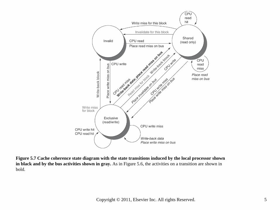
Figure 5.7 Cache coherence state diagram with the state transitions induced by the local processor shown in black and by the bus activities shown in gray. As in Figure 5.6, the activities on a transition are shown in bold.

Copyright © 2011, Elsevier Inc. All rights Reserved. 6
Figure 5.8 A multicore single-chip multiprocessor with uniform memory access through a banked sharedcache and using an interconnection network rather than a bus.

Copyright © 2011, Elsevier Inc. All rights Reserved. 7
Figure 5.11 The execution time breakdown for the three programs (OLTP, DSS, and AltaVista) in the commercial workload. The DSS numbers are the average across six different queries. The CPI varies widely from a low of 1.3 for AltaVista, to 1.61 for the DSS queries, to 7.0 for OLTP. (Individually, the DSS queries show a CPI range of 1.3 to 1.9.) “Other stalls” includes resource stalls (implemented with replay traps on the 21164), branch mispredict, memory barrier, and TLB misses. For these benchmarks, resourcebased pipeline stalls are the dominant factor. These data combine the behavior of user and kernel accesses. Only OLTP has a significant fraction of kernel accesses, and the kernel accesses tend to be better behaved than the user accesses! All the measurements shown in this section were collected by Barroso, Gharachorloo, and Bugnion [1998].

Copyright © 2011, Elsevier Inc. All rights Reserved. 8
Figure 5.12 The relative performance of the OLTP workload as the size of the L3 cache, which is set as two-way set associative, grows from 1 MB to 8 MB. The idle time also grows as cache size is increased, reducing some of the performance gains. This growth occurs because, with fewer memory system stalls, more server processes are needed to cover the I/O latency. The workload could be retuned to increase the computation/communication balance, holding the idle time in check. The PAL code is a set of sequences of specialized OS-level instructions executed in privileged mode; an example is the TLB miss handler.

Copyright © 2011, Elsevier Inc. All rights Reserved. 9
Figure 5.13 The contributing causes of memory access cycle shift as the cache size is increased. TheL3 cache is simulated as two-way set associative.

Copyright © 2011, Elsevier Inc. All rights Reserved. 10
Figure 5.14 The contribution to memory access cycles increases as processor count increases primarily due to increased true sharing. The Compulsory misses slightly increase since each processor must now handle more compulsory misses.

Copyright © 2011, Elsevier Inc. All rights Reserved. 11
Figure 5.15 The number of misses per 1000 instructions drops steadily as the block size of the L3 cache is increased,making a good case for an L3 block size of at least 128 bytes. The L3 cache is 2 MB, two-way set associative.

Copyright © 2011, Elsevier Inc. All rights Reserved. 12
Figure 5.17 The data miss rates for the user and kernel components behave differently for increases in the L1 data cache size (on the left) versus increases in the L1 data cache block size (on the right). Increasing the L1 data cache from 32 KB to 256 KB (with a 32-byte block) causes the user miss rate to decrease proportionately more than the kernel miss rate: the user- level miss rate drops by almost a factor of 3, while the kernel-level miss rate drops only by a factor of 1.3. The miss rate for both user and kernel components drops steadily as the L1 block size is increased (while keeping the L1 cache at 32 KB). In contrast to the effects of increasing the cache size, increasing the block size improves the kernel miss rate more significantly (just under a factor of 4 for the kernel references when going from 16-byte to 128-byte blocks versus just under a factor of 3 for the user references).

Copyright © 2011, Elsevier Inc. All rights Reserved. 13
Figure 5.18 The components of the kernel data miss rate change as the L1 data cache size is increased from 32 KB to 256 KB, when the multiprogramming workload is run on eight processors. The compulsory miss rate component stays constant, since it is unaffected by cache size. The capacity component drops by more than a factor of 2, while the coherence component nearly doubles. The increase in coherence misses occurs because the probability of a miss being caused by an invalidation increases with cache size, since fewer entries are bumped due to capacity. As we would expect, the increasing block size of the L1 data cache substantially reduces the compulsory miss rate in the kernel references. It also has a significant impact on the capacity miss rate, decreasing it by a factor of 2.4 over the range of block sizes. The increased block size has a small reduction in coherence traffic, which appears to stabilize at 64 bytes, with no change in the coherence miss rate in going to 128 byte lines. Because there are no significant reductions in the coherence miss rate as the block size increases, the fraction of the miss rate due to coherence grows from about 7% to about 15%.

Copyright © 2011, Elsevier Inc. All rights Reserved. 14
Figure 5.19 The number of bytes needed per data reference grows as block size is increased for both the kernel and user components. It is interesting to compare this chart against the data on scientific programs shown in Appendix I.

Copyright © 2011, Elsevier Inc. All rights Reserved. 15
Figure 5.20 A directory is added to each node to implement cache coherence in a distributed-memory multiprocessor. In this case, a node is shown as a single multicore chip, and the directory information for the associated memory may reside either on or off the multicore. Each directory is responsible for tracking the caches that share the memory addresses of the portion of memory in the node. The coherence mechanism would handle both the maintenance of the directory information and any coherence actions needed within the multicore node.

Copyright © 2011, Elsevier Inc. All rights Reserved. 16
Figure 5.22 State transition diagram for an individual cache block in a directory-based system. Requests by the local processor are shown in black, and those from the home directory are shown in gray. The states are identical to those in the snooping case, and the transactions are very similar, with explicit invalidate and write-back requests replacing the write misses that were formerly broadcast on the bus. As we did for the snooping controller, we assume that an attempt to write a shared cache block is treated as a miss; in practice, such a transaction can be treated as an ownership request or upgrade request and can deliver ownership without requiring that the cache block be fetched.

Copyright © 2011, Elsevier Inc. All rights Reserved. 17
Figure 5.23 The state transition diagram for the directory has the same states and structure as the transition diagram for an individual cache. All actions are in gray because they are all externally caused. Bold indicates the action taken by the directory in response to the request.

Copyright © 2011, Elsevier Inc. All rights Reserved. 18
Figure 5.26 A comparison of SMT and single-thread (ST) performance on the eight-processor IBM eServer p5 575. Note that the y-axis starts at a speedup of 0.9, a performance loss. Only one processor in each Power5 core is active, which should slightly improve the results from SMT by decreasing destructive interference in the memory system. The SMT results are obtained by creating 16 user threads, while the ST results use only eight threads; with only one thread per processor, the Power5 is switched to single-threaded mode by the OS. These results were collected by John McCalpin of IBM. As we can see from the data, the standard deviation of the results for the SPECfpRate is higher than for SPECintRate (0.13 versus 0.07), indicating that the SMT improvement for FP programs is likely to vary widely.
Copyright © 2011, Elsevier Inc. All rights Reserved. 19
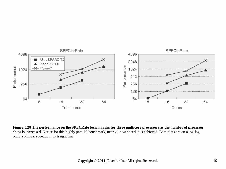
Figure 5.28 The performance on the SPECRate benchmarks for three multicore processors as the number of processor chips is increased. Notice for this highly parallel benchmark, nearly linear speedup is achieved. Both plots are on a log-log scale, so linear speedup is a straight line.

Copyright © 2011, Elsevier Inc. All rights Reserved. 20
Figure 5.29 The performance on the SPECjbb2005 benchmark for three multicore processors as the number of processorchips is increased. Notice for this parallel benchmark, nearly linear speedup is achieved.

Copyright © 2011, Elsevier Inc. All rights Reserved. 21
Figure 5.30 This chart shows the speedup for two- and four-core executions of the parallel Java and PARSEC workloads without SMT. These data were collected by Esmaeilzadeh et al. [2011] using the same setup as described in Chapter 3. Turbo Boost is turned off. The speedup and energy efficiency are summarized using harmonic mean, implying a workload where the total time spent running each 2p benchmark is equivalent.

Copyright © 2011, Elsevier Inc. All rights Reserved. 22
Figure 5.31 This chart shows the speedup for two- and four-core executions of the parallel Java and PARSEC workloads both with and without SMT. Remember that the results above vary in the number of threads from two to eight, and reflect both architectural effects and application characteristics. Harmonic mean is used to summarize results, as discussed in the caption of Figure 5.30.

Copyright © 2011, Elsevier Inc. All rights Reserved. 23
Figure 5.32 Speedup for three benchmarks on an IBM eServer p5 multiprocessor when configured with 4, 8, 16,32, and 64 processors. The dashed line shows linear speedup.

Copyright © 2011, Elsevier Inc. All rights Reserved. 24
Figure 5.33 The performance/cost relative to a 4-processor system for three benchmarks run on an IBM eServer p5 multiprocessor containing from 4 to 64 processors shows that the larger processor counts can be as cost effective as the 4- processor configuration. For TPC-C the configurations are those used in the official runs, which means that disk and memory scale nearly linearly with processor count, and a 64-processor machine is approximately twice as expensive as a 32-processor version. In contrast, the disk and memory are scaled more slowly (although still faster than necessary to achieve the best SPECRate at 64 processors). In particular, the disk configurations go from one drive for the 4-processor version to four drives (140 GB) for the 64-processor version. Memory is scaled from 8 GB for the 4-processor system to 20 GB for the 64-p-rocessor system.

Copyright © 2011, Elsevier Inc. All rights Reserved. 25
Figure 5.35 Multicore (point-to-point) multiprocessor.

Copyright © 2011, Elsevier Inc. All rights Reserved. 26
Figure 5.37 Multichip, multicore multiprocessor with DSM.

Copyright © 2011, Elsevier Inc. All rights Reserved. 27
Figure 5.38 Cache and memory states in the multichip, multicore multiprocessor.