Embed Size (px)
Citation preview

7/27/2019 Chap12-Operational Amplifier Applications
http://slidepdf.com/reader/full/chap12-operational-amplifier-applications 1/54
Jaeger/Blalock 01/05/03
Microelectronic Circuit DesignMcGraw-Hill
Chapter12
Operational Amplifier Applications
Microelectronic Circuit Design
Richard C. Jaeger
Travis N. Blalock
Chap 12 - 1

7/27/2019 Chap12-Operational Amplifier Applications
http://slidepdf.com/reader/full/chap12-operational-amplifier-applications 2/54
Jaeger/Blalock 01/05/03
Microelectronic Circuit DesignMcGraw-Hill
Chapter Goals
• Continue study of methods to determine transfer functions of circuits
containing op amps
• Introduction to active filters and switched capacitor circuits
• Explore digital-to-analog converter specifications and basic circuit
implementations
• Study analog-to-digital converter specifications and implementations
• Explore applications of op amps in nonlinear circuits, such as precision
rectifiers
• Provide examples of multivibrator circuits employing positivefeedback
• Demonstrate use of ac analysis capability of SPICE
Chapter Goals
Chap 12 - 2

7/27/2019 Chap12-Operational Amplifier Applications
http://slidepdf.com/reader/full/chap12-operational-amplifier-applications 3/54
Jaeger/Blalock 01/05/03
Microelectronic Circuit DesignMcGraw-Hill
• Op amp is voltage follower with unity
gain over a wide range of frequencies.
• Uses positive feedback through C 1 at
frequencies above dc to realize
complex poles without inductors.
• Feedback network provides dc path
for amplifier’s input bias currents.
The transfer function is:
A LP ( s)Vo
( s)Vs( s)
G1G
2
C 1C
2
s2 sG
1G
2
C 1
G
1G
2
C 1C 2
Active Filters: Low-pass
(Transfer Function)
In standard form,
A LP ( s) s2
s2 s
o
Q
o2
o 1
R1 R
2C
1C
2 Q
C 1
C 2
R1 R
2
R1 R
2
Often, circuits are designed with
C 1 = C 2 = C .
Chap 12 - 3
7/27/2019 Chap12-Operational Amplifier Applications
http://slidepdf.com/reader/full/chap12-operational-amplifier-applications 4/54
Jaeger/Blalock 01/05/03
Microelectronic Circuit DesignMcGraw-Hill
Active Filters: Low-pass
(Frequency Response)
For Q = 0.71, magnitude response is
maximally flat (Butterworth Filter:
Maximum bandwidth without peaking)
For Q >0 .71, response shows undesired
peaking.
For Q < 0.71: Filter’s bandwidth
capability is wasted.
Sensitivity, represents fractional
change in parameter P due to a given
fractional change in value of Z.Sensitivity of o with respect to R and
C is:
For << o, filter has unity gain.For >> o, response exhibits
two-pole roll-off at 40dB/decade.
At = o, gain of filter = Q.
Chap 12 - 4
S Z P
S R o S C
o 1
2
7/27/2019 Chap12-Operational Amplifier Applications
http://slidepdf.com/reader/full/chap12-operational-amplifier-applications 5/54
Jaeger/Blalock 01/05/03
Microelectronic Circuit DesignMcGraw-Hill
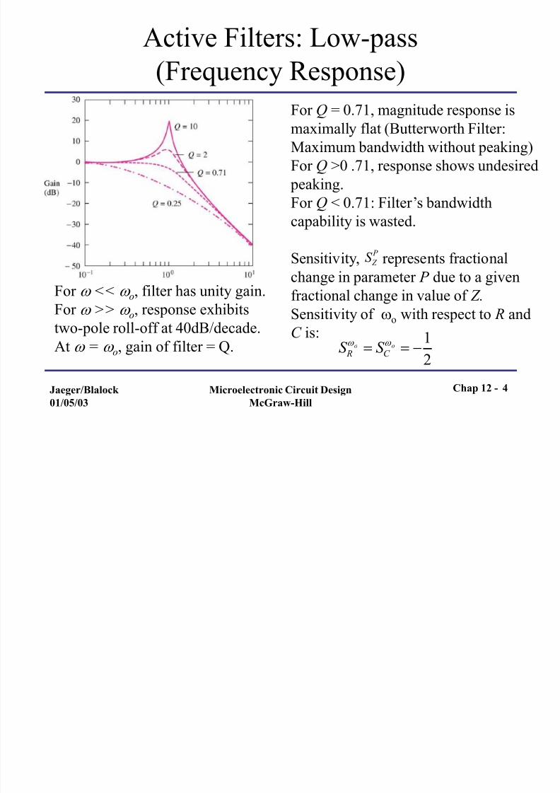
Active Filters: Low-pass (Example)
• Problem: Design second-order low-pass filter with maximally flatresponse.
• Given data: f H = 5 kHZ
• Analysis: C 1 = 2C 2 = 2C and R1 = R2 = R.
R 1
2 oC Q=
1
2
1/ oC is the reactance of C at o, R is 30% smaller than this value. Thus
impedance level of filter is set by C . If impedance level is too low, op amp
will not be able to supply current required to drive feedback network.
For a 0.01 mF capacitor at 5 kHz,
Final values: R1 = R2 = 2.26 k W,C 1 = 0.02 mF, C 2 = 0.01 mF
1
oC
1
104
(108
)
3180 W
R 3180W2
2250 W
Chap 12 - 5

7/27/2019 Chap12-Operational Amplifier Applications
http://slidepdf.com/reader/full/chap12-operational-amplifier-applications 6/54
Jaeger/Blalock 01/05/03
Microelectronic Circuit DesignMcGraw-Hill
Active Filters: High-pass with Gain
(Transfer Function)
• Voltage follower in low-pass filter
replaced by non-inverting amplifier
with gain K , which gives an added
degree of freedom in design.
• dc paths for both op amp input bias
currents through R2 and feedback
resistors.
A HP
( s) s2
s2 s
o
Q
o2
o 1
RC
Q R1
R2
C 1C
2
C 1C 2
(1 K ) R
2C
2
R1C 1
1
The transfer function is:
For R1 = R2 = R and C 1 = C 2 = C ,
o 1
RC Q=
1
3- K
For K = 3, Q is infinite; poles are on j axis causing sinusoidal oscillations.
K > 3 causes instability due to right-
half plane poles.31 K
Chap 12 - 6

7/27/2019 Chap12-Operational Amplifier Applications
http://slidepdf.com/reader/full/chap12-operational-amplifier-applications 7/54
Jaeger/Blalock 01/05/03
Microelectronic Circuit DesignMcGraw-Hill
Active Filters: High-pass with Gain
(Frequency Response)
• For Q = 0.71, magnitude response is maximally flat (Butterworth Filter
response).
• Amplifier gain is constant for > o, the lower cutoff frequency of
the filter.
Chap 12 - 7

7/27/2019 Chap12-Operational Amplifier Applications
http://slidepdf.com/reader/full/chap12-operational-amplifier-applications 8/54
Jaeger/Blalock 01/05/03
Microelectronic Circuit DesignMcGraw-Hill
Active Filters: Band-pass
(Transfer Function)
Gth
V th
s C 1C
2
G
th
V
1( s) sC
1V
o( s)
A BP ( s) V o( s)
V th( s)
R3
R1 R
3
R2C 2 R
1C
1
s o s2 s
o
Q
o2
o 1
Rth R
2C
1C
2
QR
2
Rth
C 1C
2
C 1C
2
For C 1 = C 2 = C ,
o 1
C Rth R
2
QR
2
Rth
BW 2
R2C
Uses inverting op amp and its full loop gain
(ideally infinite).
sC 2V1( s)Vo
( s) R
2
Chap 12 - 8

7/27/2019 Chap12-Operational Amplifier Applications
http://slidepdf.com/reader/full/chap12-operational-amplifier-applications 9/54
Jaeger/Blalock 01/05/03
Microelectronic Circuit DesignMcGraw-Hill
Active Filters: Band-pass
(Frequency Response)
• Response peaks at o and gain at center frequency is 2Q2
.• For << o or >> o, filter response corresponds to single-pole
high-pass or low-pass filter changing at a rate of ±20dB/decade.
Chap 12 - 9
7/27/2019 Chap12-Operational Amplifier Applications
http://slidepdf.com/reader/full/chap12-operational-amplifier-applications 10/54
Jaeger/Blalock 01/05/03
Microelectronic Circuit DesignMcGraw-Hill
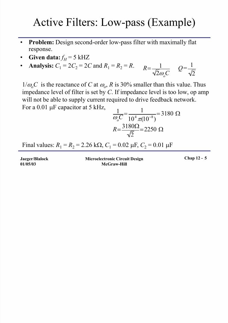
Active Filters: Tow-Thomas Biquad
T ( s) a2 s2a
1 sa
0
s2 s
o
Q
o2
General biquadratic transfer function
to represent low-pass, high-pass,
band-pass, all-pass and notch filters:
In Tow-Thomas biquad, first op amp
is a multi-input integrator and third
op amp is simply an inverter.
V bp( s) 1
sR1C
V s( s) 1
sRC -V
lp( s)
1
sR2
C V
bp( s)
V lp( s)
1
sRC V
bp( s)
Abp
( s) K s
o
s2 s oQ o2
K R R
1
o
1
RC Q
R2
RBW
1
R2
C
Alp( s) K
o2
s2 s
o
Q
o
2
Thus, center frequency, Q
and gain can each be
adjusted independently.
Chap 12 - 10

7/27/2019 Chap12-Operational Amplifier Applications
http://slidepdf.com/reader/full/chap12-operational-amplifier-applications 11/54
7/27/2019 Chap12-Operational Amplifier Applications
http://slidepdf.com/reader/full/chap12-operational-amplifier-applications 12/54
Jaeger/Blalock 01/05/03
Microelectronic Circuit DesignMcGraw-Hill
Active Filters: Tow-Thomas Biquad
(Example)
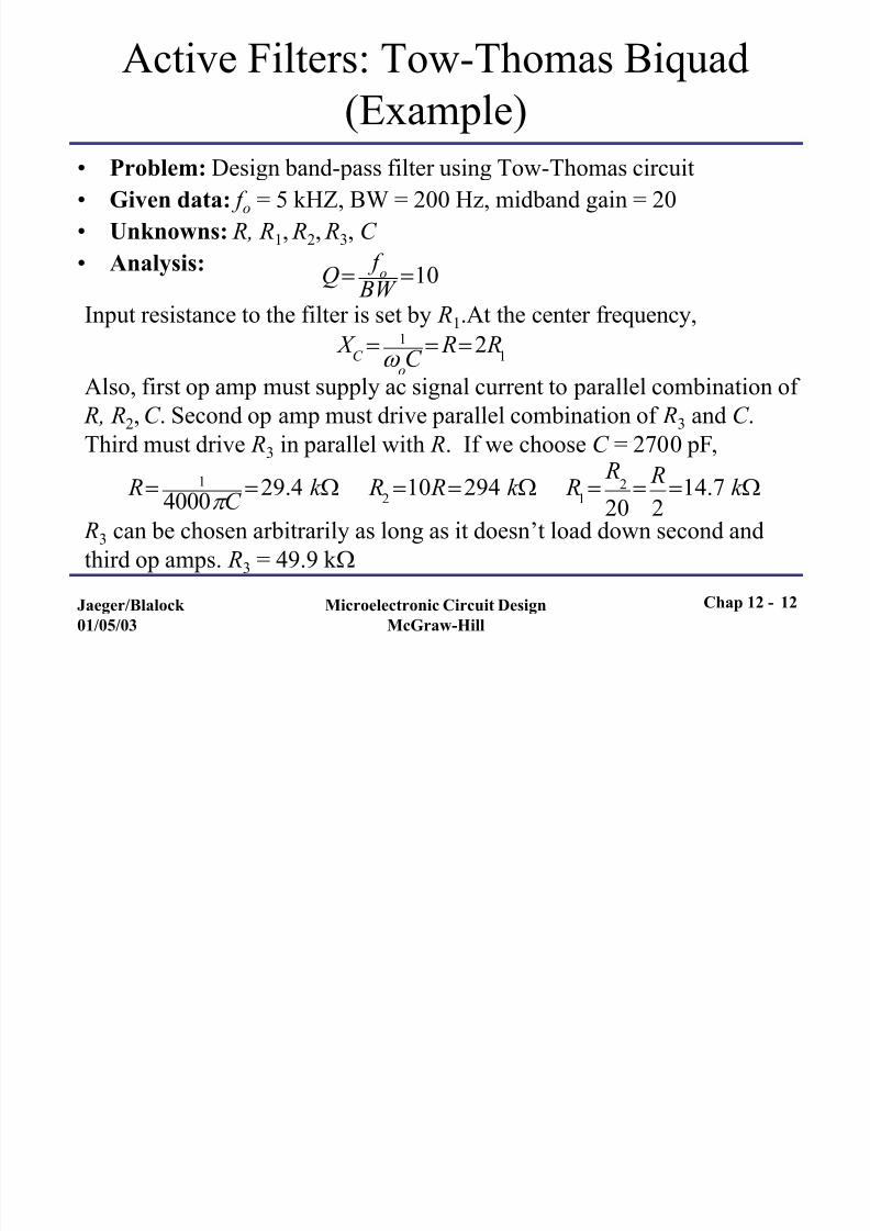
• Problem: Design band-pass filter using Tow-Thomas circuit
• Given data: f o = 5 kHZ, BW = 200 Hz, midband gain = 20
• Unknowns: R, R1, R2, R3, C
• Analysis:
Q f o
BW 10
R 1
4000 C 29.4 k W R
210 R294 k W R
1
R2
20 R
214.7 k W
Input resistance to the filter is set by R1.At the center frequency,
Also, first op amp must supply ac signal current to parallel combination of
R, R2, C . Second op amp must drive parallel combination of R3 and C .
Third must drive R3 in parallel with R. If we choose C = 2700 pF,
R3 can be chosen arbitrarily as long as it doesn’t load down second and
third op amps. R3 = 49.9 k W
X C
1
oC
R2 R1
Chap 12 - 12
7/27/2019 Chap12-Operational Amplifier Applications
http://slidepdf.com/reader/full/chap12-operational-amplifier-applications 13/54
Jaeger/Blalock 01/05/03
Microelectronic Circuit DesignMcGraw-Hill
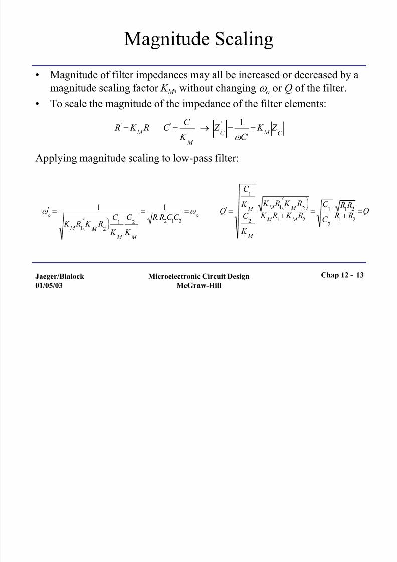
Magnitude Scaling
• Magnitude of filter impedances may all be increased or decreased by a
magnitude scaling factor K M , without changing o or Q of the filter.
• To scale the magnitude of the impedance of the filter elements:
Applying magnitude scaling to low-pass filter:
R' K M
R C ' C
K M
Z C
' 1
C '
K M
Z C
o' 1
K M
R1
K M
R2
C 1
K M
C 2
K M
1 R
1 R
2C 1C 2
o Q'
C 1
K M
C 2
K M
K M
R1
K M
R2
K M
R1
K M
R2
C 1
C 2
R1 R2 R
1 R
2Q
Chap 12 - 13

7/27/2019 Chap12-Operational Amplifier Applications
http://slidepdf.com/reader/full/chap12-operational-amplifier-applications 14/54
Jaeger/Blalock 01/05/03
Microelectronic Circuit DesignMcGraw-Hill
Frequency Scaling
• Cutoff or center frequencies of filter may be scaled by a frequencyscaling factor K F without changing Q of the filter if each capacitor value is divided by K F and resistor values are left unchanged.
Applying frequency scaling to low-pass filter:
R' R C ' C
K F
o
' 1
R1 R
2C 1
K F
C 2
K F
K
F
R1 R2C 1C 2
K F
o
Q'
C 1
K F
C 2
K F
R1 R
2
R1 R2
C 1
C 2
R1 R
2
R1 R2
Q
Chap 12 - 14

7/27/2019 Chap12-Operational Amplifier Applications
http://slidepdf.com/reader/full/chap12-operational-amplifier-applications 15/54
Jaeger/Blalock 01/05/03
Microelectronic Circuit DesignMcGraw-Hill
Switched-Capacitor Circuits
• Switched-capacitor (SC) circuits eliminate resistors in filters by
replacing them with capacitors and switches
• Resulting filters are discrete-time or sampled-data equivalents of
the continuous-time filters discussed so far
• Provide additional flexibility not readily available in continuous-
time form, such as inversion of signal polarity without using an
amplifier
• SC circuits are compatible with high density MOS IC processes• SC circuits provide low-pass filters and CMOS ICs for signal
processing and communications applications
Chap 12 - 15

7/27/2019 Chap12-Operational Amplifier Applications
http://slidepdf.com/reader/full/chap12-operational-amplifier-applications 16/54
Jaeger/Blalock 01/05/03
Microelectronic Circuit DesignMcGraw-Hill
SC Integrator
During phase 1, input voltage is sampled and
output is constant. In phase 2, output changes
to reflect sampled information in phase 1.
Charge stored in phase 1 is:
Q1
C 1V
S
V S
vS
n1 T
Voltage stored on C 1 at
end of sampling interval
Change in charge stored
on C 2 in phase 2.Q
2C
2v
O
vO
C 1
C 2
V S
vO
nT vO(n 1)T
C 1
C 2
vS (n 1)T
Output voltage at end of nth clock cycle is:
Chap 12 - 16

7/27/2019 Chap12-Operational Amplifier Applications
http://slidepdf.com/reader/full/chap12-operational-amplifier-applications 17/54
Jaeger/Blalock 01/05/03
Microelectronic Circuit DesignMcGraw-Hill
Equivalence Between SC Integrator and
Continuous-Time Integrator
Consider total charge Q s flowing from source vS through resistor R during clock period T . For simplicity, assume vS is constant: vS = V S .
Equating this charge to charge stored on C 1
f C is clock frequency.
For a capacitance of 1 pF and a switching frequency of 100 kHz, theequivalent resistance is 10 MW,which is much larger than resistorsthat can be realized in ICs.
Q s IT V s R
T
sV C T R sV
1
1
1
1C
C f C
T R
Chap 12 - 17
7/27/2019 Chap12-Operational Amplifier Applications
http://slidepdf.com/reader/full/chap12-operational-amplifier-applications 18/54
Jaeger/Blalock 01/05/03
Microelectronic Circuit DesignMcGraw-Hill
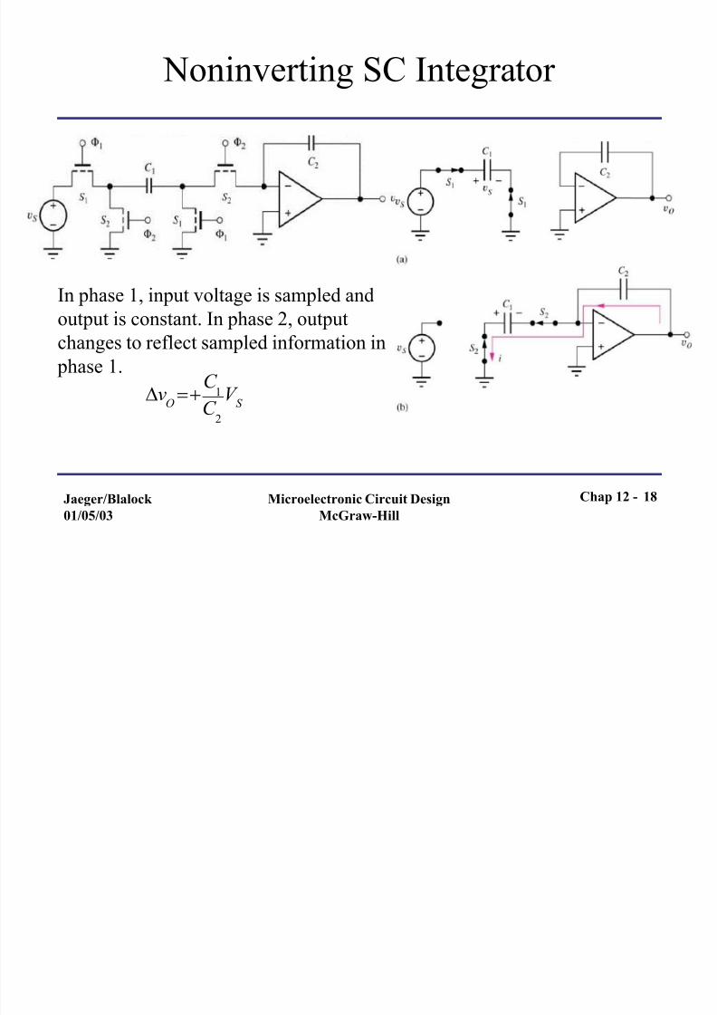
Noninverting SC Integrator
In phase 1, input voltage is sampled and
output is constant. In phase 2, output
changes to reflect sampled information in
phase 1.
vO
C 1C
2
V S
Chap 12 - 18

7/27/2019 Chap12-Operational Amplifier Applications
http://slidepdf.com/reader/full/chap12-operational-amplifier-applications 19/54
Jaeger/Blalock 01/05/03
Microelectronic Circuit DesignMcGraw-Hill
Stray-Insensitive SC Circuits
In phase 1, source is connected to summing
junction of op amp, charge C 1V s is delivered to
C 2. Node 1 is driven by and node 2 is kept at
zero.
In phase 2, source is disconnected, output is
constant and C 1 is totally discharged. Any stray
capacitances at nodes 1 or 2 don’t introduce
errors into charge transfer process.
vO
C 1
C 2
V S
Chap 12 - 19

7/27/2019 Chap12-Operational Amplifier Applications
http://slidepdf.com/reader/full/chap12-operational-amplifier-applications 20/54
Jaeger/Blalock 01/05/03
Microelectronic Circuit DesignMcGraw-Hill
Switched-Capacitor Band-Pass Filter
Rth T C
3
R2 T C
4
o1
T
C 3C
4
C 1C 2
f C
C 3C
4
C 1C 2
QC
3
C 4
C 1C
2
C 1C
2
Center frequency is tunable just by changingclock frequency, Q is independent of frequency.
But, SC filters are sampled-data systems. Hence,
due to sampling theorem,
f f
C 2
Chap 12 - 20

7/27/2019 Chap12-Operational Amplifier Applications
http://slidepdf.com/reader/full/chap12-operational-amplifier-applications 21/54
Jaeger/Blalock 01/05/03
Microelectronic Circuit DesignMcGraw-Hill
Switched-Capacitor
Tow-Thomas Biquad
• Ability of SC circuits to change polarities without an amplifier
eliminate one op amp in the SC implementation.
Chap 12 - 21

7/27/2019 Chap12-Operational Amplifier Applications
http://slidepdf.com/reader/full/chap12-operational-amplifier-applications 22/54
Jaeger/Blalock 01/05/03
Microelectronic Circuit DesignMcGraw-Hill
Digital-to-Analog (D/A) Converters
Fundamentals
• In a DAC, an n-bit binary input word (b1,b2,…bn) is combined withreference voltage V REF to give output of the DAC.
• Full-scale voltage V FS is related to V REF of the converter by V FS = KV REF
where K determines converter gain commonly set to 1.
• V OS, the offset voltage of the converter characterizes the DAC outputwhen the digital input code is zero. Offset voltage is normally adjustedto zero.
• The smallest voltage change at DAC output occurs when the LSB bn in
the digital word changes from a 0 to 1 and is also called resolution.
• b1, the MSB has a weight of one-half V FS.
vO
V FS (b
121b
222...b
n2n)V
OS b
i 1,0
V LSB
2nV FS
Chap 12 - 22

7/27/2019 Chap12-Operational Amplifier Applications
http://slidepdf.com/reader/full/chap12-operational-amplifier-applications 23/54
Jaeger/Blalock 01/05/03
Microelectronic Circuit DesignMcGraw-Hill
D/A Converter Specifications
Offset and Gain Errors
• Maximum output of ideal converter is
always 1 LSB smaller than V FS.
• For shown ideal DAC characteristic,
0.875 V FS corresponds to maximum
output code of 111.
• Gain error of converter represents
deviation of slope of converter transfer
function from that of corresponding
ideal DAC.
• Shown ideal DAC has been calibrated
so that V OS = 0 and 1 LSB is V FS /8.• Offset voltage is output of converter for
zero binary input code.
Chap 12 - 23
7/27/2019 Chap12-Operational Amplifier Applications
http://slidepdf.com/reader/full/chap12-operational-amplifier-applications 24/54
Jaeger/Blalock 01/05/03
Microelectronic Circuit DesignMcGraw-Hill
D/A Converter Specifications
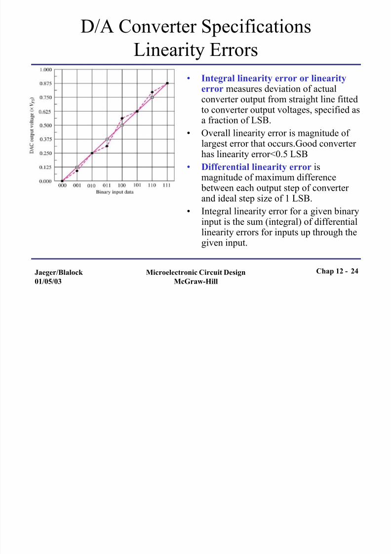
Linearity Errors
• Integral linearity error or linearityerror measures deviation of actualconverter output from straight line fittedto converter output voltages, specified asa fraction of LSB.
• Overall linearity error is magnitude of largest error that occurs.Good converter has linearity error<0.5 LSB
• Differential linearity error ismagnitude of maximum difference between each output step of converter and ideal step size of 1 LSB.
• Integral linearity error for a given binaryinput is the sum (integral) of differentiallinearity errors for inputs up through thegiven input.
Chap 12 - 24

7/27/2019 Chap12-Operational Amplifier Applications
http://slidepdf.com/reader/full/chap12-operational-amplifier-applications 25/54
Jaeger/Blalock 01/05/03
Microelectronic Circuit DesignMcGraw-Hill
D/A Converter Specifications
Monotonicity
• If the output of the DAC does not
increase in a monotonic manner if the
input code is increased, the DAC is
said to be non monotonic.
• It is possible for a monotonic
converter to have a differential
linearity error >1 LSB but, a non-
monotonic converter always has a
differential linearity error > 1 LSB
Chap 12 - 25

7/27/2019 Chap12-Operational Amplifier Applications
http://slidepdf.com/reader/full/chap12-operational-amplifier-applications 26/54
Jaeger/Blalock 01/05/03
Microelectronic Circuit DesignMcGraw-Hill
Weighted-Resistor DAC
Drawbacks:
• Need to have accurate resistor ratios over a wide range of resistor values.
• Switches in series withresistors require zero offsetvoltage and low on-resistance.
• Current drawn form referencevaries with input patterncausing change in voltage drop
in Thévenin equivalent sourceresistance of reference leadingto data-dependent errors calledsuperposition errors.
Binary input data controls the switches.
Successive resistors are progressively
weighted by a factor of 2 producing:
Linearity errors arise due to improper resistor
ratios, op amp offset voltage adds to V OS of
converter.
vO V REF(b121b222...bn2n)
Chap 12 - 26

7/27/2019 Chap12-Operational Amplifier Applications
http://slidepdf.com/reader/full/chap12-operational-amplifier-applications 27/54
Jaeger/Blalock 01/05/03
Microelectronic Circuit DesignMcGraw-Hill
R-2R Ladder
• Avoids weighted-resistor DAC problem
of wide range of resistor values
• Well-suited to IC realization as itrequires matching of only two resistor
values, R and 2 R
• The contribution of each
bit is reduced by a factor
of 2 going from MSB to
LSB
Drawbacks:
• Requires switches with
low on-resistance and zero
offset voltage
• Current drawn from
reference varies depending
on input data pattern
Chap 12 - 27

7/27/2019 Chap12-Operational Amplifier Applications
http://slidepdf.com/reader/full/chap12-operational-amplifier-applications 28/54
Jaeger/Blalock 01/05/03
Microelectronic Circuit DesignMcGraw-Hill
Inverted R-2R Ladder
• Currents in ladder and reference are independent of digital input
• Complementary currents are available at output of inverted ladder
• Switches still need to have low on-resistance to minimize errors
Chap 12 - 28

7/27/2019 Chap12-Operational Amplifier Applications
http://slidepdf.com/reader/full/chap12-operational-amplifier-applications 29/54
Jaeger/Blalock 01/05/03
Microelectronic Circuit DesignMcGraw-Hill
Inherently Monotonic DAC
• Analog switch tree connects desired
tap to input of an op amp operating
as a voltage follower.
• Each tap on resistor network is
forced to produce voltage greater than or equal to the taps below it ,
forcing the output to increase
monotonically as the digital input
code increases.
• An 8-bit version requires 256equal-valued resistors, 510 switches
and additional decoding logic.
Chap 12 -
29

7/27/2019 Chap12-Operational Amplifier Applications
http://slidepdf.com/reader/full/chap12-operational-amplifier-applications 30/54
Jaeger/Blalock 01/05/03
Microelectronic Circuit DesignMcGraw-Hill
Switched-Capacitor DACs
• Since circuits consist only of capacitors
and switches, static power dissipation
occurs only in the op amps.
• Dynamic switching losses occur.
• When switch changes state, current
impulses charge/discharge network
capacitors, changing voltage on feedback
capacitor by an amount corresponding to
bit weight of switch that changed state.
• Circuits represent direct SC analogs of weighted-resistor and R-2R ladder
DACs. Power consumption is very low.
Chap 12 -
30

7/27/2019 Chap12-Operational Amplifier Applications
http://slidepdf.com/reader/full/chap12-operational-amplifier-applications 31/54
Jaeger/Blalock 01/05/03 Microelectronic Circuit DesignMcGraw-Hill
DACs in Bipolar Technology
Bipolar transistors aren’t good voltage switches due to their inherent offset voltage in
saturation, but they are very good current sources and switches.
• Currents switched into summing junction, supplied through R F , determine output voltage of theDAC.
• V BE of current-source transistors must be same for proper weighting of current sources,
requiring equal current densities in the transistors. Thus, the area of each transistor is raised by
factor of 2 from LSB to MSB.
Chap 12 -
31
7/27/2019 Chap12-Operational Amplifier Applications
http://slidepdf.com/reader/full/chap12-operational-amplifier-applications 32/54
Jaeger/Blalock 01/05/03 Microelectronic Circuit DesignMcGraw-Hill
DACs in Bipolar Technology (cont.)
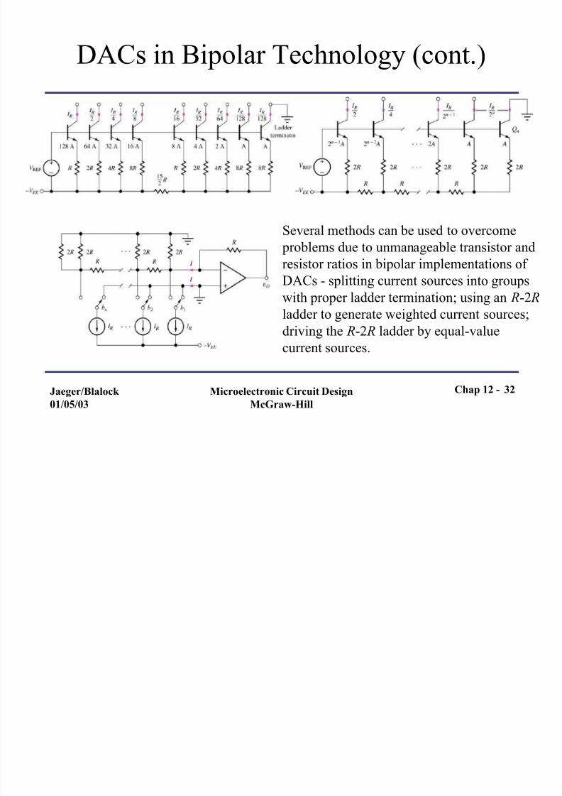
Several methods can be used to overcome
problems due to unmanageable transistor and
resistor ratios in bipolar implementations of
DACs - splitting current sources into groups
with proper ladder termination; using an R-2 R ladder to generate weighted current sources;
driving the R-2 R ladder by equal-value
current sources.
Chap 12 -
32
7/27/2019 Chap12-Operational Amplifier Applications
http://slidepdf.com/reader/full/chap12-operational-amplifier-applications 33/54
Jaeger/Blalock 01/05/03 Microelectronic Circuit DesignMcGraw-Hill
Reference Current Circuitry for Bipolar
Implementations of DACs
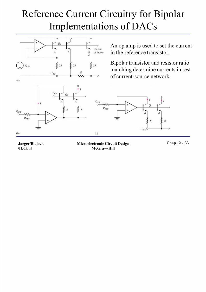
An op amp is used to set the current
in the reference transistor.
Bipolar transistor and resistor ratio
matching determine currents in rest
of current-source network.
Chap 12 -
33

7/27/2019 Chap12-Operational Amplifier Applications
http://slidepdf.com/reader/full/chap12-operational-amplifier-applications 34/54
Jaeger/Blalock 01/05/03 Microelectronic Circuit DesignMcGraw-Hill
Analog -to-Digital (A/D) Converters
Fundamentals
• ADC takes unknown continuous analog input signal, mostly voltagev X and converts it into n-bit binary number, which is a binary fractionrepresenting ratio between unknown input voltage and full-scalevoltage
• For given output code, we know that value of input voltage lies withina 1-LSB quantization interval.
V FS
KV REF
Quantization error occurs due to
initial underestimation and then
overestimation of input voltage by
output code.
Ideal ADC should pick values of bits
in binary word to minimizemagnitude of quantization error:
v v
X (b
121b
222 ...b
n2n )V
FS
Chap 12 -
34

7/27/2019 Chap12-Operational Amplifier Applications
http://slidepdf.com/reader/full/chap12-operational-amplifier-applications 35/54
Jaeger/Blalock 01/05/03 Microelectronic Circuit DesignMcGraw-Hill
A/D Converter Specifications
Offset and Gain Errors
• Differential linearity error is difference
between actual code step width and ideal
step size of 1 LSB.
• ADC with differential linearity error<
1LSB has no missing codes.
• Gain error is deviation of slope of
converter transfer function from that of
corresponding ideal ADC.
• Shown ADC characteristic has offset
error of 0.5LSB first transition occurs at
a 0.5LSB higher voltage.• Good ADC is monotonic with linearity
error<0.5LSB and no missing codes over
full temperature range.
• Integral linearity error or linearity
error is deviation of code transition
points from their ideal positions.
• Integral linearity error is sum of
differential linearity errors for individual
steps.
Chap 12 -
35

7/27/2019 Chap12-Operational Amplifier Applications
http://slidepdf.com/reader/full/chap12-operational-amplifier-applications 36/54
Jaeger/Blalock 01/05/03 Microelectronic Circuit DesignMcGraw-Hill
A/D Conversion Techniques
• If v X > vREF, output voltage is high corresponding to logic 1.
• If v X < vREF, output voltage is high corresponding to logic 0.
vREF is time-dependent reference voltage, varied till unknown input is
determined within quantization error of converter.
Ideally ADC logic chooses bi so that
v X
V FS
bi2i
i 1
n
V FS
2n 1
Chap 12 -
36
7/27/2019 Chap12-Operational Amplifier Applications
http://slidepdf.com/reader/full/chap12-operational-amplifier-applications 37/54
Jaeger/Blalock 01/05/03 Microelectronic Circuit DesignMcGraw-Hill
Counting ADC
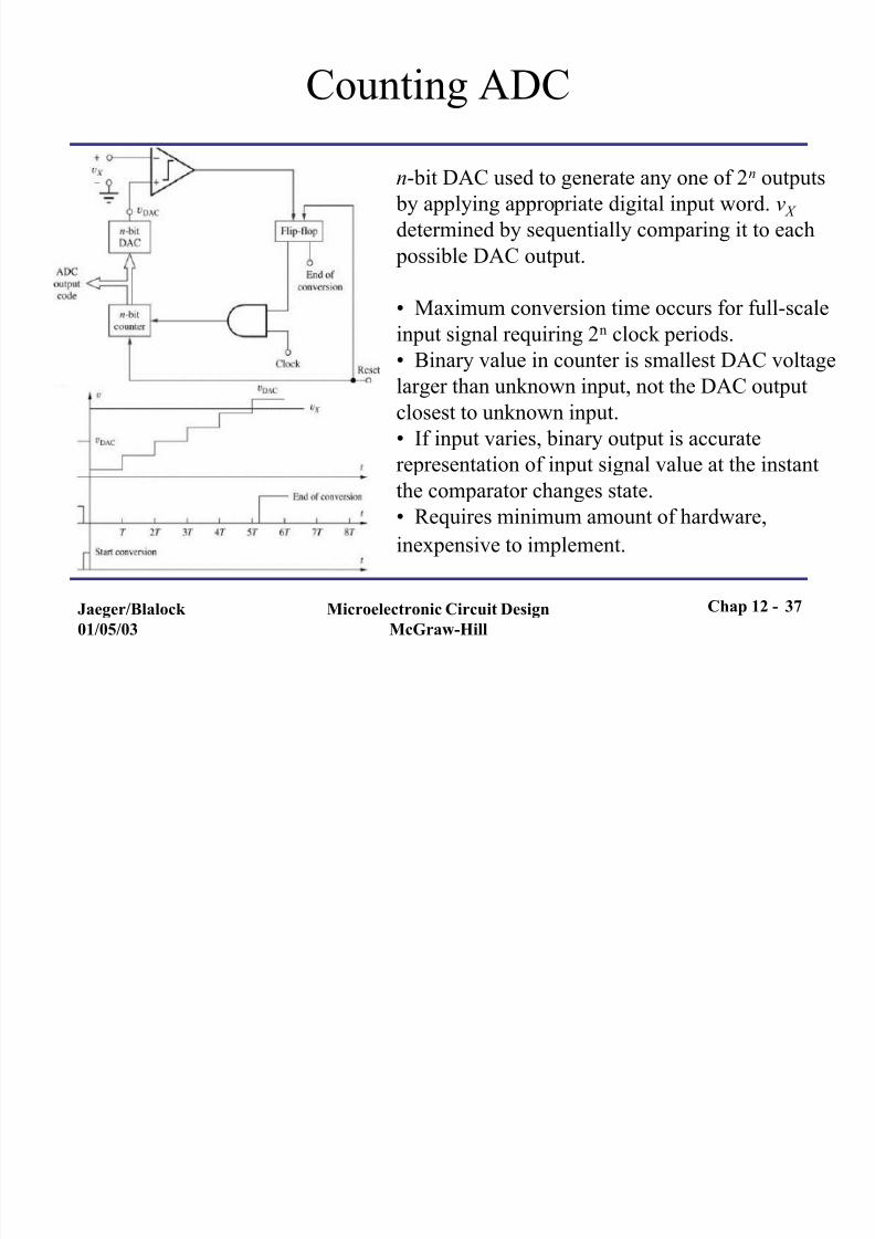
n-bit DAC used to generate any one of 2n outputs
by applying appropriate digital input word. v X
determined by sequentially comparing it to each
possible DAC output.
•Maximum conversion time occurs for full-scale
input signal requiring 2n clock periods.
• Binary value in counter is smallest DAC voltage
larger than unknown input, not the DAC output
closest to unknown input.
• If input varies, binary output is accurate
representation of input signal value at the instantthe comparator changes state.
• Requires minimum amount of hardware,
inexpensive to implement.
Chap 12 -
37

7/27/2019 Chap12-Operational Amplifier Applications
http://slidepdf.com/reader/full/chap12-operational-amplifier-applications 38/54
Jaeger/Blalock 01/05/03 Microelectronic Circuit DesignMcGraw-Hill
Successive Approximation ADC
•Binary search used by SAL to determine v X .
•n-bit conversion needs n clock periods. Speed limited by
time taken by DAC output to settle within a fraction of an
LSB of V FS and by comparator to respond to input signals
differing by small amounts.
•Slowly varying input signals not changing by more than
0.5 LSB (V FS /2n+1 ) during conversion time (T T = nT C ) are
acceptable.
•For a sinusoidal input signal with p-p amplitude V FS ,
•To avoid this frequency limitation, high speed sample-
and-hold circuit is used ahead of the successive
approximation ADC.
•Very popular ADC with fast conversion times, used in 8-
to 16- bit converters
f O
f O
2n 2n
Chap 12 -
38

7/27/2019 Chap12-Operational Amplifier Applications
http://slidepdf.com/reader/full/chap12-operational-amplifier-applications 39/54
Jaeger/Blalock 01/05/03 Microelectronic Circuit DesignMcGraw-Hill
Single-Ramp (Single-Slope) ADC
•Reference voltage varies linearly with a well-
defines slope from slightly below 0 to above V FS
if K= V FS / 2nT C .
•Maximum conversion time occurs for full-scale
input signal requiring 2n clock periods.•Counter output is value of v X at the time end-
of-conversion signal occurs.
•Ramp voltage can be generated using an
integrator connected to a constant reference
voltage.
•Dependence of ramp’s slope on RC productwhich is susceptible to changes due to
temperature variations or aging is a limitation of
this ADC.
v X
KNT C
v
X
V FS
N
2n
Chap 12 -
39

7/27/2019 Chap12-Operational Amplifier Applications
http://slidepdf.com/reader/full/chap12-operational-amplifier-applications 40/54
Jaeger/Blalock 01/05/03 Microelectronic Circuit DesignMcGraw-Hill
Dual-Ramp (Dual-Slope) ADC
T 12nT C T 2 NT C
1
RC v
X (t )dt
0
T 1
1
RC V REF
(t )dt T 1
T 1
T 2
v
X
V REF
T 2
T 1
N
2n
•Absolute values of R and C don’t affect
operation.
•Digital output word gives average value of v X
during first integration phase.
•Conversion time is given by:
•Can be used to get resolutions exceeding 20
bits but at lower conversion rates.
T T
(2n N )T C
2n 1T C
Chap 12 -
40

7/27/2019 Chap12-Operational Amplifier Applications
http://slidepdf.com/reader/full/chap12-operational-amplifier-applications 41/54
Jaeger/Blalock 01/05/03 Microelectronic Circuit DesignMcGraw-Hill
Dual-Ramp (Dual-Slope) ADC (cont.)
• Integrator in dual-ramp ADC has thenormalized transfer function shown.
• Sinusoidal inputs with frequencies thatare exact multiples of 1/T 1, have
integrals of zero and don’t appear atintegrator output. This property iscalled normal-mode rejection.
• Recent dual-slope ADCs include extraintegration phases for automatic offsetelimination.
• Triple ramp ADC uses coarse and finedown ramps to improve speed byfactor of 2n/ 2 for n-bit dual-rampconverter.
Chap 12 -
41

7/27/2019 Chap12-Operational Amplifier Applications
http://slidepdf.com/reader/full/chap12-operational-amplifier-applications 42/54
Jaeger/Blalock 01/05/03 Microelectronic Circuit DesignMcGraw-Hill
Parallel or Flash ADC
• Unknown input simultaneously compared to 7
different reference voltages (3-bit converter).
Logic network encodes comparator outputs
into 3-bit binary output representing quantized
value of input voltage.
• Very high speed ( up to 108-109
conversions/sec) limited only by delays of
comparators and logic network.
• Output continuously reflects input delayed by
comparator and logic network.
• Requires 2n-1 comparators and referencevoltages for n-bit conversion. Used for
resolutions up to 10 bits.
Chap 12 - 42
7/27/2019 Chap12-Operational Amplifier Applications
http://slidepdf.com/reader/full/chap12-operational-amplifier-applications 43/54
Jaeger/Blalock 01/05/03 Microelectronic Circuit DesignMcGraw-Hill
Delta Sigma ADCs
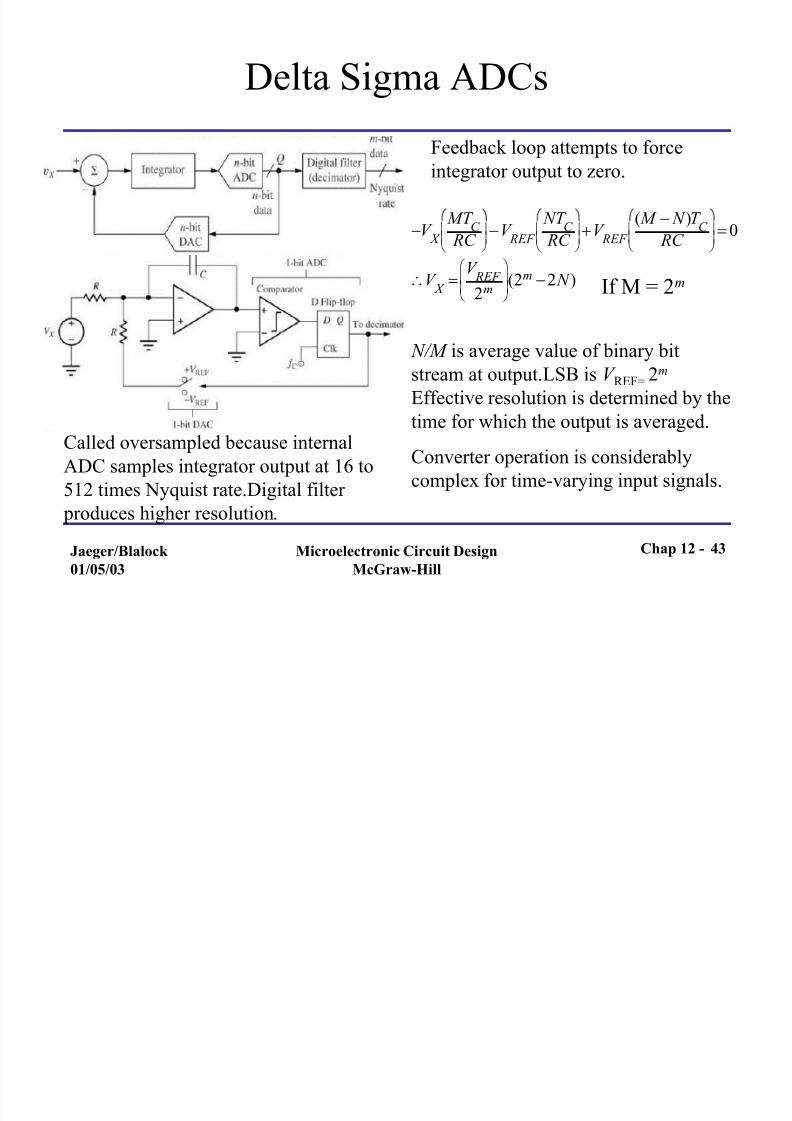
Called oversampled because internal
ADC samples integrator output at 16 to
512 times Nyquist rate.Digital filter
produces higher resolution.
V X
MT C
RC
V
REF
NT C
RC
V
REF
( M N )T C
RC
0
V X
V REF 2m
(2m
2 N ) If M = 2m
N/M is average value of binary bit
stream at output.LSB is V REF= 2m
Effective resolution is determined by the
time for which the output is averaged.
Converter operation is considerably
complex for time-varying input signals.
Feedback loop attempts to forceintegrator output to zero.
Chap 12 - 43
7/27/2019 Chap12-Operational Amplifier Applications
http://slidepdf.com/reader/full/chap12-operational-amplifier-applications 44/54
Jaeger/Blalock
01/05/03
Microelectronic Circuit Design
McGraw-Hill
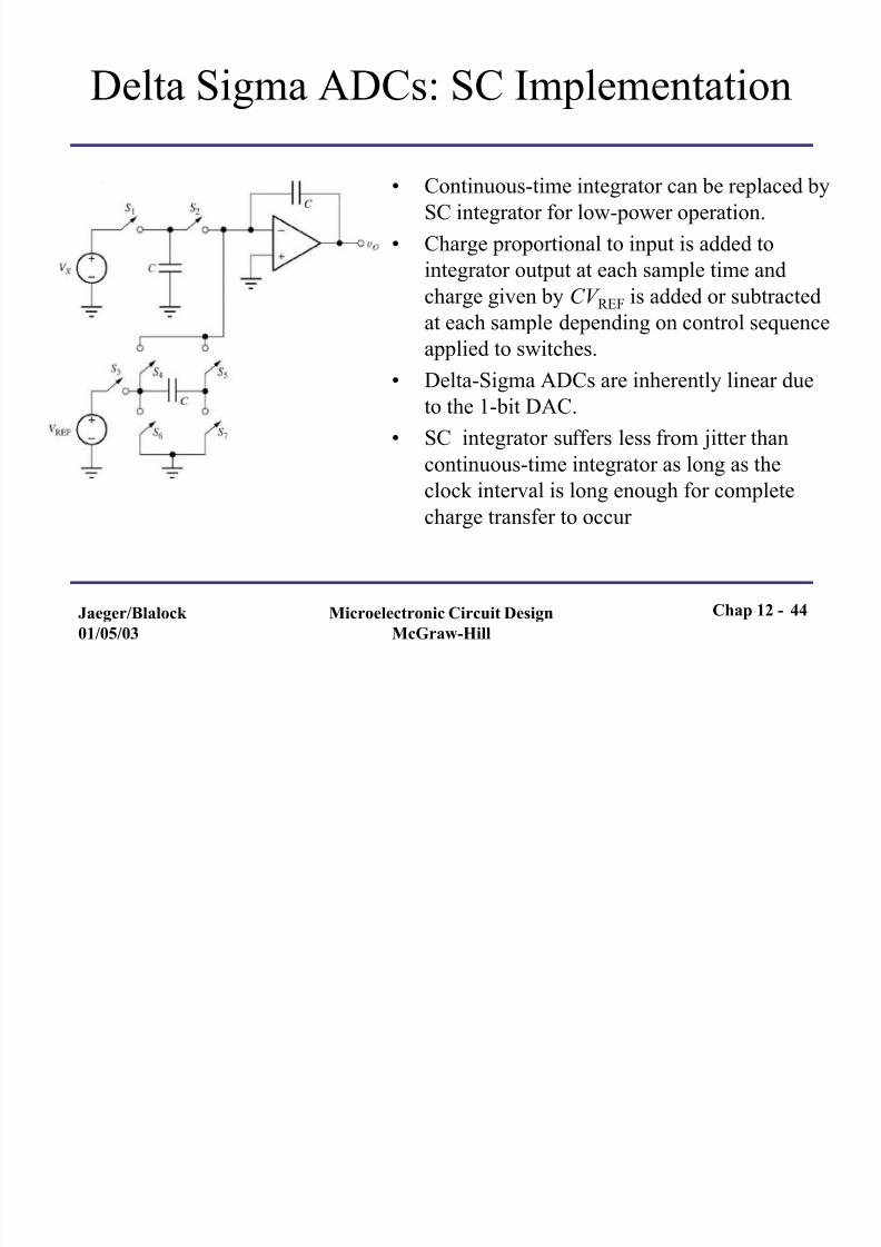
Delta Sigma ADCs: SC Implementation
• Continuous-time integrator can be replaced by
SC integrator for low-power operation.
• Charge proportional to input is added to
integrator output at each sample time and
charge given by CV REF is added or subtracted
at each sample depending on control sequence
applied to switches.
• Delta-Sigma ADCs are inherently linear due
to the 1-bit DAC.
• SC integrator suffers less from jitter than
continuous-time integrator as long as theclock interval is long enough for complete
charge transfer to occur
Chap 12 - 44

7/27/2019 Chap12-Operational Amplifier Applications
http://slidepdf.com/reader/full/chap12-operational-amplifier-applications 45/54
Jaeger/Blalock
01/05/03
Microelectronic Circuit Design
McGraw-Hill
Nonlinear Circuit Applications:
Precision Half-Wave Rectifier
• For vS > 0, vO = vS , i > 0, diode isforward-biased and feedback loop isclosed. Rectification is perfect even for small input voltages..
• For vS < 0,diode is cutoff, i = 0, vO = 0.
• Primary sources of error are gain error and offset error due to nonideal op amp.
• For negative input voltages, outputvoltage v1 is saturated at negative limit.Large negative voltages across input can
destroy unprotected op amps.• Response time of circuit is slowed down
due to slow recovery of internal circuitsfrom saturation.
vO is rectified replica of vS
without loss of voltage drop as
in diode rectifier circuit.
Chap 12 - 45

7/27/2019 Chap12-Operational Amplifier Applications
http://slidepdf.com/reader/full/chap12-operational-amplifier-applications 46/54
Jaeger/Blalock
01/05/03
Microelectronic Circuit Design
McGraw-Hill
Nonlinear Circuit Applications: Non-
Saturating Precision Half-Wave Rectifier
• For vS > 0, v1 is negative (one diode-
drop below zero), D2 is forward biased,
current in R2 is zero, vO = 0, D1 is
reverse biased. Feedback loop is closedthrough D2.
• For vS < 0, v1 is one diode-drop above
output voltage, diode D1 turns on, D2 is
off. Circuit behaves as inverting
amplifier with gain - R2
/ R1. Feedback
loop is closed through D1 and R2.
Chap 12 - 46
7/27/2019 Chap12-Operational Amplifier Applications
http://slidepdf.com/reader/full/chap12-operational-amplifier-applications 47/54
Jaeger/Blalock
01/05/03
Microelectronic Circuit Design
McGraw-Hill
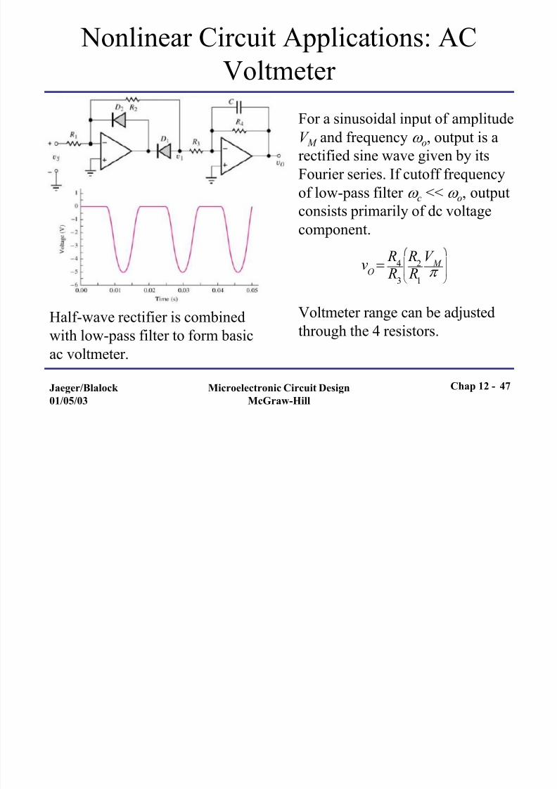
Nonlinear Circuit Applications: AC
Voltmeter
Half-wave rectifier is combined
with low-pass filter to form basic
ac voltmeter.
For a sinusoidal input of amplitude
V M and frequency o, output is a
rectified sine wave given by its
Fourier series. If cutoff frequency
of low-pass filter c << o, outputconsists primarily of dc voltage
component.
Voltmeter range can be adjusted
through the 4 resistors.
vO R
4
R3
R2
R1
V M
Chap 12 - 47

7/27/2019 Chap12-Operational Amplifier Applications
http://slidepdf.com/reader/full/chap12-operational-amplifier-applications 48/54
Jaeger/Blalock
01/05/03
Microelectronic Circuit Design
McGraw-Hill
Circuits with Positive Feedback
Comparator
• For inputs > V REF, output saturates at V CC .
• For inputs < V REF, output saturates at -V EE .
• Amplifiers built for use as comparators can
handle saturation at the voltage extremes
without incurring excessive internal time
delays.
• For noisy inputs, multiple transitions may
occur as input signal crosses reference level.
Chap 12 - 48
7/27/2019 Chap12-Operational Amplifier Applications
http://slidepdf.com/reader/full/chap12-operational-amplifier-applications 49/54
Jaeger/Blalock
01/05/03
Microelectronic Circuit Design
McGraw-Hill
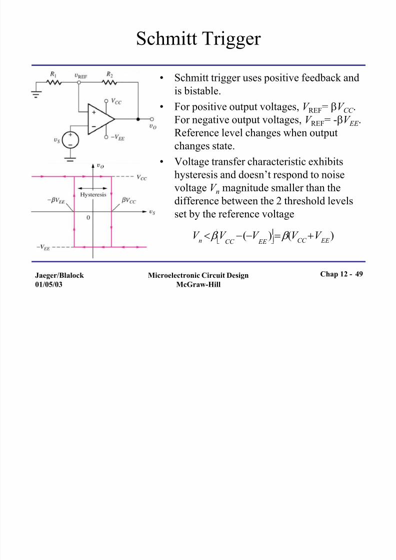
Schmitt Trigger
• Schmitt trigger uses positive feedback and
is bistable.
• For positive output voltages, V REF= bV CC .
For negative output voltages, V REF= -bV EE .
Reference level changes when output
changes state.
• Voltage transfer characteristic exhibits
hysteresis and doesn’t respond to noise
voltage V n magnitude smaller than the
difference between the 2 threshold levels
set by the reference voltage
V n
b V CC
(V EE
)
b (V
CC V
EE )
Chap 12 - 49

7/27/2019 Chap12-Operational Amplifier Applications
http://slidepdf.com/reader/full/chap12-operational-amplifier-applications 50/54
Jaeger/Blalock
01/05/03
Microelectronic Circuit Design
McGraw-Hill
Astable Multivibrator
• Uses positive and negative
feedback to generate rectangular output.
• Output voltage switches
periodically between V CC and -V EE .
For symmetrical power supplies,
output of circuit is square wave with
period T
T T 1T
22 RC ln
1 b 1 b
Chap 12 - 50

7/27/2019 Chap12-Operational Amplifier Applications
http://slidepdf.com/reader/full/chap12-operational-amplifier-applications 51/54
Jaeger/Blalock
01/05/03
Microelectronic Circuit Design
McGraw-Hill
Astable Multivibrator (cont.)
• Astable multivibrator can be used to generate square, triangular andsine wave outputs as shown at frequencies up to few MHz.
• Frequency is varied by changing R3 or C 3. C 3 is often changed in
decade steps. R3 may be varied continuously using potentiometer.
Chap 12 - 51

7/27/2019 Chap12-Operational Amplifier Applications
http://slidepdf.com/reader/full/chap12-operational-amplifier-applications 52/54
Jaeger/Blalock
01/05/03
Microelectronic Circuit Design
McGraw-Hill
Monostable Multivibrator or One Shot
• Operates with one stable state, generatessingle pulse of known duration on application
of trigger signal.• D1 couples trigger signal into circuit,
clamping diode D2 limits negative voltageexcursion on capacitor C .
Chap 12 - 52
7/27/2019 Chap12-Operational Amplifier Applications
http://slidepdf.com/reader/full/chap12-operational-amplifier-applications 53/54
Jaeger/Blalock
01/05/03
Microelectronic Circuit Design
McGraw-Hill
Monostable Multivibrator (cont.)
• Output of circuit consists of positive pulse with fixed duration T given by
• For well-defined pulse, circuit should not be triggered till voltages on all nodes
return to their quiescent steady-state values.
• Recovery time (return of circuit to state before trigger pulse was applied) is
given by:
T RC ln
1V
D
V CC
1 b
T r RC ln
1 b V
CC
V EE
1V
D
V EE
Chap 12 - 53
7/27/2019 Chap12-Operational Amplifier Applications
http://slidepdf.com/reader/full/chap12-operational-amplifier-applications 54/54
Jaeger/Blalock Microelectronic Circuit Design
End of Chapter 12