Embed Size (px)
Citation preview
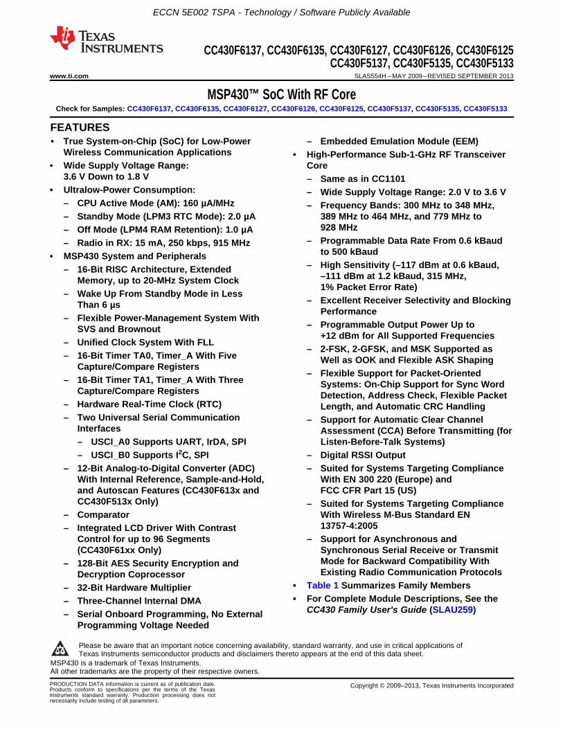
ECCN 5E002 TSPA - Technology / Software Publicly Available
CC430F6137, CC430F6135, CC430F6127, CC430F6126, CC430F6125CC430F5137, CC430F5135, CC430F5133
www.ti.com SLAS554H –MAY 2009–REVISED SEPTEMBER 2013
MSP430™ SoC With RF CoreCheck for Samples: CC430F6137, CC430F6135, CC430F6127, CC430F6126, CC430F6125, CC430F5137, CC430F5135, CC430F5133
1FEATURES23• True System-on-Chip (SoC) for Low-Power – Embedded Emulation Module (EEM)
Wireless Communication Applications • High-Performance Sub-1-GHz RF Transceiver• Wide Supply Voltage Range: Core
3.6 V Down to 1.8 V – Same as in CC1101• Ultralow-Power Consumption: – Wide Supply Voltage Range: 2.0 V to 3.6 V
– CPU Active Mode (AM): 160 µA/MHz – Frequency Bands: 300 MHz to 348 MHz,– Standby Mode (LPM3 RTC Mode): 2.0 µA 389 MHz to 464 MHz, and 779 MHz to
928 MHz– Off Mode (LPM4 RAM Retention): 1.0 µA– Programmable Data Rate From 0.6 kBaud– Radio in RX: 15 mA, 250 kbps, 915 MHz
to 500 kBaud• MSP430 System and Peripherals– High Sensitivity (–117 dBm at 0.6 kBaud,– 16-Bit RISC Architecture, Extended
–111 dBm at 1.2 kBaud, 315 MHz,Memory, up to 20-MHz System Clock1% Packet Error Rate)
– Wake Up From Standby Mode in Less– Excellent Receiver Selectivity and BlockingThan 6 µs
Performance– Flexible Power-Management System With
– Programmable Output Power Up toSVS and Brownout+12 dBm for All Supported Frequencies
– Unified Clock System With FLL– 2-FSK, 2-GFSK, and MSK Supported as
– 16-Bit Timer TA0, Timer_A With Five Well as OOK and Flexible ASK ShapingCapture/Compare Registers
– Flexible Support for Packet-Oriented– 16-Bit Timer TA1, Timer_A With Three Systems: On-Chip Support for Sync Word
Capture/Compare Registers Detection, Address Check, Flexible Packet– Hardware Real-Time Clock (RTC) Length, and Automatic CRC Handling– Two Universal Serial Communication – Support for Automatic Clear Channel
Interfaces Assessment (CCA) Before Transmitting (for– USCI_A0 Supports UART, IrDA, SPI Listen-Before-Talk Systems)– USCI_B0 Supports I2C, SPI – Digital RSSI Output
– 12-Bit Analog-to-Digital Converter (ADC) – Suited for Systems Targeting ComplianceWith Internal Reference, Sample-and-Hold, With EN 300 220 (Europe) andand Autoscan Features (CC430F613x and FCC CFR Part 15 (US)CC430F513x Only) – Suited for Systems Targeting Compliance
– Comparator With Wireless M-Bus Standard EN13757‑‑4:2005– Integrated LCD Driver With Contrast
Control for up to 96 Segments – Support for Asynchronous and(CC430F61xx Only) Synchronous Serial Receive or Transmit
Mode for Backward Compatibility With– 128-Bit AES Security Encryption andExisting Radio Communication ProtocolsDecryption Coprocessor
• Table 1 Summarizes Family Members– 32-Bit Hardware Multiplier• For Complete Module Descriptions, See the– Three-Channel Internal DMA
CC430 Family User's Guide (SLAU259)– Serial Onboard Programming, No ExternalProgramming Voltage Needed
1
Please be aware that an important notice concerning availability, standard warranty, and use in critical applications ofTexas Instruments semiconductor products and disclaimers thereto appears at the end of this data sheet.
2MSP430 is a trademark of Texas Instruments.3All other trademarks are the property of their respective owners.PRODUCTION DATA information is current as of publication date. Copyright © 2009–2013, Texas Instruments IncorporatedProducts conform to specifications per the terms of the TexasInstruments standard warranty. Production processing does notnecessarily include testing of all parameters.

ECCN 5E002 TSPA - Technology / Software Publicly Available
CC430F6137, CC430F6135, CC430F6127, CC430F6126, CC430F6125CC430F5137, CC430F5135, CC430F5133SLAS554H –MAY 2009–REVISED SEPTEMBER 2013 www.ti.com
APPLICATIONS• Wireless Analog and Digital Sensor Systems• Heat Cost Allocators• Thermostats• AMR or AMI Metering• Smart Grid Wireless Networks
DESCRIPTIONThe Texas Instruments CC430 family of ultralow-power microcontroller system-on-chip (SoC) with integrated RFtransceiver cores consists of several devices featuring different sets of peripherals targeted for a wide range ofapplications. The architecture, combined with five low-power modes, is optimized to achieve extended battery lifein portable measurement applications. The device features the powerful MSP430 16-bit RISC CPU, 16-bitregisters, and constant generators that contribute to maximum code efficiency.
The CC430 family provides a tight integration between the microcontroller core, its peripherals, software, and theRF transceiver, making these true SoC solutions easy to use as well as improving performance.
The CC430F61xx series are microcontroller SoC configurations that combine the excellent performance of thestate-of-the-art CC1101 sub-1-GHz RF transceiver with the MSP430 CPUXV2, up to 32KB of in-systemprogrammable flash memory, up to 4KB of RAM, two 16-bit timers, a high-performance 12-bit analog-to-digitalconverter (ADC) with eight external inputs plus internal temperature and battery sensors on CC430F613xdevices, a comparator, universal serial communication interfaces (USCIs), a 128-bit AES security accelerator, ahardware multiplier, a DMA, a real-time clock (RTC) module with alarm capabilities, an LCD driver, and up to44 I/O pins.
The CC430F513x series are microcontroller SoC configurations that combine the excellent performance of thestate-of-the-art CC1101 sub-1-GHz RF transceiver with the MSP430 CPUXV2, up to 32KB of in-systemprogrammable flash memory, up to 4KB of RAM, two 16-bit timers, a high performance 12-bit ADC with sixexternal inputs plus internal temperature and battery sensors, a comparator, universal serial communicationinterfaces (USCIs), a 128-bit AES security accelerator, a hardware multiplier, a DMA, an RTC module with alarmcapabilities, and up to 30 I/O pins.
Typical applications for these devices include wireless analog and digital sensor systems, heat cost allocators,thermostats, metering (AMR or AMI), and smart grid wireless networks.
Table 1 summarizes the available family members.
For complete module descriptions, see the CC430 Family User's Guide (SLAU259).
2 Submit Documentation Feedback Copyright © 2009–2013, Texas Instruments Incorporated
Product Folder Links: CC430F6137 CC430F6135 CC430F6127 CC430F6126 CC430F6125 CC430F5137CC430F5135 CC430F5133

ECCN 5E002 TSPA - Technology / Software Publicly Available
CC430F6137, CC430F6135, CC430F6127, CC430F6126, CC430F6125CC430F5137, CC430F5135, CC430F5133
www.ti.com SLAS554H –MAY 2009–REVISED SEPTEMBER 2013
Table 1. Family Members (1) (2)
USCIProgram PackageChannel A: Channel B:Device SRAM (KB) Timer_A (3) LCD_B (4) ADC12_A (4) Comp_B I/O(KB) TypeUART, LIN, SPI, I2C
IrDA, SPI
8 ext,CC430F6137 32 4 5, 3 96 seg 1 1 8 ch. 44 64 RGC4 int ch.
8 ext,CC430F6135 16 2 5, 3 96 seg 1 1 8 ch. 44 64 RGC4 int ch.
CC430F6127 32 4 5, 3 96 seg 1 1 n/a 8 ch. 44 64 RGC
CC430F6126 32 2 5, 3 96 seg 1 1 n/a 8 ch. 44 64 RGC
CC430F6125 16 2 5, 3 96 seg 1 1 n/a 8 ch. 44 64 RGC
6 ext,CC430F5137 32 4 5, 3 n/a 1 1 6 ch. 30 48 RGZ4 int ch.
6 ext,CC430F5135 16 2 5, 3 n/a 1 1 6 ch. 30 48 RGZ4 int ch.
6 ext,CC430F5133 8 2 5, 3 n/a 1 1 6 ch. 30 48 RGZ4 int ch.
(1) For the most current package and ordering information, see the Package Option Addendum at the end of this document, or see the TIweb site at www.ti.com.
(2) Package drawings, thermal data, and symbolization are available at www.ti.com/packaging.(3) Each number in the sequence represents an instantiation of Timer_A with its associated number of capture compare registers and PWM
output generators available. For example, a number sequence of 5, 3 would represent two instantiations of Timer_A, the firstinstantiation having 5 and the second instantiation having 3 capture compare registers and PWM output generators, respectively.
(4) n/a = not available
Copyright © 2009–2013, Texas Instruments Incorporated Submit Documentation Feedback 3
Product Folder Links: CC430F6137 CC430F6135 CC430F6127 CC430F6126 CC430F6125 CC430F5137CC430F5135 CC430F5133

RAM
4kB2kB
Power
Mgmt
LDO
SVM/SVS
Brownout
SYS
TA0
5 CC
Registers
EEM
(S: 3+1)
RTC_A
Comp_B
Flash
32kB
16kB
SMCLK
ACLK
MDB
MAB
XOUTXIN
Spy-Bi-
Wire
CRC16
Bus
Cntrl
Logic
MAB
MDB
MAB
MDB
MCLK
USCI_A0
(UART,
IrDA, SPI)
USCI_B0
(SPI, I2C)
LCD_B
96
Segments
1,2,3,4
Mux
I/O Ports
P1/P2
2x8 I/Os
PA
1x16 I/Os
P1.x/P2.x
2x8
I/O Ports
P3/P4
2x8 I/Os
PB
1x16 I/Os
P3.x/P4.x
2x8
I/O Ports
P5
1x8 I/Os
P5.x
1x8
AES128
Security
En-/De-
cryption
RF_XOUTRF_XIN
RF_NRF_P
TA1
3 CC
Registers
MODEM
RF/ANALOG
TX & RX
Frequency
Synthesizer
CPU Interface
Packet
Handler
Digital RSSI
Carrier Sense
PQI / LQI
CCA
Sub-1GHz
Radio
(CC1101)
MPY32
ADC12
(32kHz) (26MHz)
Unified
Clock
System
CPUXV2incl. 16
Registers
JTAG
Interface
DMA
Controller
3 Channel
PortMappingController
Watch-dog
REF
VoltageReference
ECCN 5E002 TSPA - Technology / Software Publicly Available
CC430F6137, CC430F6135, CC430F6127, CC430F6126, CC430F6125CC430F5137, CC430F5135, CC430F5133SLAS554H –MAY 2009–REVISED SEPTEMBER 2013 www.ti.com
CC430F613x Functional Block Diagram
4 Submit Documentation Feedback Copyright © 2009–2013, Texas Instruments Incorporated
Product Folder Links: CC430F6137 CC430F6135 CC430F6127 CC430F6126 CC430F6125 CC430F5137CC430F5135 CC430F5133

RGC PACKAGE(TOP VIEW)
CC430F613x
P3.7
/PM
_S
MC
LK
/S17
P2.0
/PM
_C
BO
UT
1/P
M_TA
1C
LK
/CB
0/A
0
17
64P
3.6
/PM
_R
FG
DO
1/S
16
P2.1
/PM
_TA
1C
CR
0A
/CB
1/A
1
18
63P
3.5
/PM
_TA
0C
CR
4A
/S15
P2.2
/PM
_TA
1C
CR
1A
/CB
2/A
2
19
62
P2.3
/PM
_TA
1C
CR
2A
/CB
3/A
3P
3.4
/PM
_TA
0C
CR
3A
/S14
20
61
P2.4
/PM
_R
TC
CLK
/CB
4/A
4/V
RE
F-/
VeR
EF
-P
3.3
/PM
_TA
0C
CR
2A
/S13
21
60
P2.5
//C
B5/A
5P
M_S
VM
OU
T/V
RE
F+
/VeR
EF
+P
3.2
/PM
_TA
0C
CR
1A
/S12
22
59
DV
CC
P4.4
/S6
29
52
RS
T/N
MI/S
BW
TD
IOP
4.3
/S5
30
51
TE
ST
/SB
WT
CK
P4.2
/S4
31
50
PJ.3
/TC
KP
4.1
/S3
32
49
P2.6
/PM
_A
CLK
/CB
6/A
6P
3.1
/PM
_TA
0C
CR
0A
/S11
23
58
P2.7
//C
B7/A
7P
M_A
DC
12C
LK
/PM
_D
MA
E0
P3.0
/PM
_C
BO
UT
0/P
M_TA
0C
LK
/S10
24
57
AV
CC
DV
CC
25
56
P5.0
/XIN
P4.7
/S9
26
55
P5.1
/XO
UT
P4.6
/S8
27
54
AV
SS
P4.5
/S7
28
53
P4.0/S2P1.0/PM_RFGDO0/S18 3316
P5.3/S1P1.1/PM_RFGDO2/S19 3415
P5.2/S0P1.2/PM_UCB0SOMI/PM_UCB0SCL/S20 3514
RF_XINP1.3/PM_UCB0SIMO/PM_UCB0SDA/S21 3613
RF_XOUTP1.4/PM_UCB0CLK/PM_UCA0STE/S22 3712
AVCC_RFDVCC 3811
GUARDLCDCAP/R33 454
PJ.0/TDOP1.5/PM_UCA0RXD/PM_UCA0SOMI/R23 463
PJ.1/TDI/TCLKP1.6/PM_UCA0TXD/PM_UCA0SIMO/R13/LCDREF 472
PJ.2/TMSP1.7/PM_UCA0CLK/PM_UCB0STE/R03 481
AVCC_RFVCORE 3910
RF_PP5.4/S23 409
RF_NP5.5/COM3/S24 418
AVCC_RFP5.6/COM2/S25 427
AVCC_RFP5.7/COM1/S26 436
R_BIASCOM0 445
VSSExposed dieattached pad
ECCN 5E002 TSPA - Technology / Software Publicly Available
CC430F6137, CC430F6135, CC430F6127, CC430F6126, CC430F6125CC430F5137, CC430F5135, CC430F5133
www.ti.com SLAS554H –MAY 2009–REVISED SEPTEMBER 2013
NOTE: The secondary digital functions on ports P1, P2, and P3 are fully mappable. This pinout shows only the defaultmapping. See Table 9 for details.
CAUTION: The LCDCAP/R33 must be connected to VSS if not used.
Copyright © 2009–2013, Texas Instruments Incorporated Submit Documentation Feedback 5
Product Folder Links: CC430F6137 CC430F6135 CC430F6127 CC430F6126 CC430F6125 CC430F5137CC430F5135 CC430F5133

RAM
4kB2kB2kB
Power
Mgmt
LDO
SVM/SVS
Brownout
TA0
5 CC
Registers
EEM
(S: 3+1)
RTC_A
Comp_B
Flash
32kB32kB16kB
SMCLK
ACLK
MDB
MAB
XOUTXIN
Spy-Bi-
Wire
CRC16
Bus
Cntrl
Logic
MAB
MDB
MAB
MDB
MCLK
USCI_A0
(UART,
IrDA, SPI)
USCI_B0
(SPI, I2C)
LCD_B
96
Segments
1,2,3,4
Mux
I/O Ports
P1/P2
2x8 I/Os
PA
1x16 I/Os
P1.x/P2.x
2x8
I/O Ports
P3/P4
2x8 I/Os
PB
1x16 I/Os
P3.x/P4.x
2x8
I/O Ports
P5
1x8 I/Os
P5.x
1x8
AES128
Security
En-/De-
cryption
RF_XOUTRF_XIN
RF_NRF_P
TA1
3 CC
Registers
MODEM
RF/ANALOG
TX & RX
Frequency
Synthesizer
CPU Interface
Packet
Handler
Digital RSSI
Carrier Sense
PQI / LQI
CCA
Sub-1GHz
Radio
(CC1101)
MPY32
(32kHz) (26MHz)
Unified
Clock
System
JTAG
Interface
DMA
Controller
3 Channel
SYS
PortMappingController
Watch-dog
REF
VoltageReference
CPUXV2incl. 16
Registers
ECCN 5E002 TSPA - Technology / Software Publicly Available
CC430F6137, CC430F6135, CC430F6127, CC430F6126, CC430F6125CC430F5137, CC430F5135, CC430F5133SLAS554H –MAY 2009–REVISED SEPTEMBER 2013 www.ti.com
CC430F612x Functional Block Diagram
6 Submit Documentation Feedback Copyright © 2009–2013, Texas Instruments Incorporated
Product Folder Links: CC430F6137 CC430F6135 CC430F6127 CC430F6126 CC430F6125 CC430F5137CC430F5135 CC430F5133

RGC PACKAGE(TOP VIEW)
CC430F612x
P3.7
/PM
_S
MC
LK
/S17
P2.0
/PM
_C
BO
UT
1/P
M_TA
1C
LK
/CB
0
17
64P
3.6
/PM
_R
FG
DO
1/S
16
P2.1
/PM
_TA
1C
CR
0A
/CB
1
18
63P
3.5
/PM
_TA
0C
CR
4A
/S15
P2.2
/PM
_TA
1C
CR
1A
/CB
2
19
62
P2.3
/PM
_TA
1C
CR
2A
/CB
3P
3.4
/PM
_TA
0C
CR
3A
/S14
20
61
P2.4
/PM
_R
TC
CLK
/CB
4P
3.3
/PM
_TA
0C
CR
2A
/S13
21
60
P2.5
//C
B5
PM
_S
VM
OU
TP
3.2
/PM
_TA
0C
CR
1A
/S12
22
59
DV
CC
P4.4
/S6
29
52
RS
T/N
MI/S
BW
TD
IOP
4.3
/S5
30
51
TE
ST
/SB
WT
CK
P4.2
/S4
31
50
PJ.3
/TC
KP
4.1
/S3
32
49
P2.6
/PM
_A
CLK
/CB
6P
3.1
/PM
_TA
0C
CR
0A
/S11
23
58
P2.7
//C
B7
PM
_D
MA
E0
P3.0
/PM
_C
BO
UT
0/P
M_TA
0C
LK
/S10
24
57
AV
CC
DV
CC
25
56
P5.0
/XIN
P4.7
/S9
26
55
P5.1
/XO
UT
P4.6
/S8
27
54
AV
SS
P4.5
/S7
28
53
P4.0/S2P1.0/PM_RFGDO0/S18 3316
P5.3/S1P1.1/PM_RFGDO2/S19 3415
P5.2/S0P1.2/PM_UCB0SOMI/PM_UCB0SCL/S20 3514
RF_XINP1.3/PM_UCB0SIMO/PM_UCB0SDA/S21 3613
RF_XOUTP1.4/PM_UCB0CLK/PM_UCA0STE/S22 3712
AVCC_RFDVCC 3811
GUARDLCDCAP/R33 454
PJ.0/TDOP1.5/PM_UCA0RXD/PM_UCA0SOMI/R23 463
PJ.1/TDI/TCLKP1.6/PM_UCA0TXD/PM_UCA0SIMO/R13/LCDREF 472
PJ.2/TMSP1.7/PM_UCA0CLK/PM_UCB0STE/R03 481
AVCC_RFVCORE 3910
RF_PP5.4/S23 409
RF_NP5.5/COM3/S24 418
AVCC_RFP5.6/COM2/S25 427
AVCC_RFP5.7/COM1/S26 436
R_BIASCOM0 445
VSSExposed dieattached pad
ECCN 5E002 TSPA - Technology / Software Publicly Available
CC430F6137, CC430F6135, CC430F6127, CC430F6126, CC430F6125CC430F5137, CC430F5135, CC430F5133
www.ti.com SLAS554H –MAY 2009–REVISED SEPTEMBER 2013
NOTE: The secondary digital functions on ports P1, P2, and P3 are fully mappable. This pinout shows only the defaultmapping. See Table 9 for details.
CAUTION: The LCDCAP/R33 must be connected to VSS if not used.
Copyright © 2009–2013, Texas Instruments Incorporated Submit Documentation Feedback 7
Product Folder Links: CC430F6137 CC430F6135 CC430F6127 CC430F6126 CC430F6125 CC430F5137CC430F5135 CC430F5133
RAM
4kB
2kB
Power
Mgmt
LDO
SVM/SVS
Brownout
TA0
5 CCRegisters
EEM
(S: 3+1)
RTC_A
Comp_B
Flash
32kB16kB8kB
SMCLK
ACLK
MDB
MAB
XOUTXIN
Spy-Bi-
Wire
CRC16
Bus
Cntrl
Logic
MAB
MDB
MAB
MDB
MCLK
USCI_A0
(UART,
IrDA, SPI)
USCI_B0
(SPI, I2C)
I/O Ports
P1/P2
2x8 I/Os
PA
1x16 I/Os
P1.x/P2.x
2x8
I/O Ports
P3
1x8 I/Os
P3.x
1x8
I/O Ports
P5
1x2 I/Os
P5.x
1x2
AES128
Security
En-/De-
cryption
RF_XOUTRF_XIN
RF_NRF_P
MODEM
RF/ANALOG
TX & RX
Frequency
Synthesizer
CPU Interface
Packet
Handler
Digital RSSI
Carrier Sense
PQI / LQI
CCA
Sub-1GHz
Radio
(CC1101)
MPY32
ADC12
(32kHz) (26MHz)
Unified
Clock
System
JTAG
Interface
DMA
Controller
3 Channel
SYS
PortMappingController
Watch-dog
REF
VoltageReference
CPUXV2incl. 16
Registers
TA1
3 CCRegisters
ECCN 5E002 TSPA - Technology / Software Publicly Available
CC430F6137, CC430F6135, CC430F6127, CC430F6126, CC430F6125CC430F5137, CC430F5135, CC430F5133SLAS554H –MAY 2009–REVISED SEPTEMBER 2013 www.ti.com
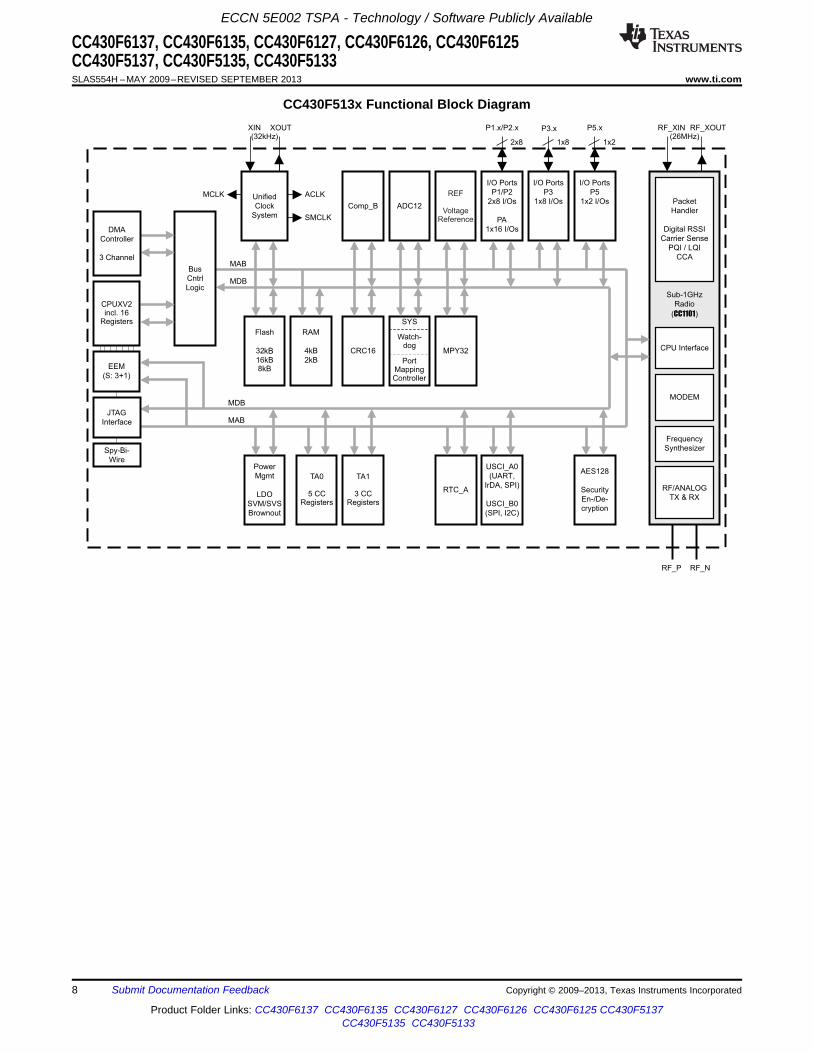
CC430F513x Functional Block Diagram
8 Submit Documentation Feedback Copyright © 2009–2013, Texas Instruments Incorporated
Product Folder Links: CC430F6137 CC430F6135 CC430F6127 CC430F6126 CC430F6125 CC430F5137CC430F5135 CC430F5133

RGZ PACKAGE(TOP VIEW)
12
11
4
3
2
1
10
9
8
7
6
5
13 14 15 16 17 18 19 20 21 22 23 2425
26
27
28
29
30
31
32
33
34
35
3648 47 46 45 44 43 42 41 40 39 38 37
P1.1/PM_RFGDO2
P1.2/PM_UCB0SOMI/PM_UCB0SCL
P1.7/PM_UCA0CLK/PM_UCB0STE
P2.0/PM_CBOUT1/PM_TA1CLK/CB0/A0
P2.1/PM_TA1CCR0A/CB1/A1
P2.2/PM_TA1CCR1A/CB2/A2
P1.3/PM_UCB0SIMO/PM_UCB0SDA
P1.4/PM_UCB0CLK/PM_UCA0STE
DVCC
VCORE
P1.5/PM_UCA0RXD/PM_UCA0SOMI
P1.6/PM_UCA0TXD/PM_UCA0SIMO
RF_XIN
RF_XOUT
AVCC_RF
GUARD
PJ.0/TDO
PJ.1/TDI/TCLK
AVCC_RF
RF_P
RF_N
AVCC_RF
AVCC_RF
R_BIAS
P2.3
/PM
_TA
1C
CR
2A
/CB
3/A
3
P2.4
/PM
_R
TC
CLK
/CB
4/A
4/V
RE
F-/
VeR
EF
-
RS
T/N
MI/S
BW
TD
IO
TE
ST
/SB
WT
CK
PJ.3
/TC
K
PJ.2
/TM
S
P2.5
/PM
_S
VM
OU
T/C
B5/A
5/V
RE
F+
/VeR
EF
+
AV
CC
P5.0
/XIN
P5.1
/XO
UT
AV
SS
DV
CC
P1.0
/PM
_R
FG
DO
0
P3.7
/PM
_S
MC
LK
P3.6
/PM
_R
FG
DO
1
P3.5
/PM
_TA
0C
CR
4A
P3.4
/PM
_TA
0C
CR
3A
P3.3
/PM
_TA
0C
CR
2A
P3.2
/PM
_TA
0C
CR
1A
P3.1
/PM
_TA
0C
CR
0A
P3.0
/PM
_C
BO
UT
0/P
M_TA
0C
LK
DV
CC
P2.7
/PM
_A
DC
12C
LK
/PM
_D
MA
E0
P2.6
/PM
_A
CLK
VSSExposed dieattached pad
CC430F513x
ECCN 5E002 TSPA - Technology / Software Publicly Available
CC430F6137, CC430F6135, CC430F6127, CC430F6126, CC430F6125CC430F5137, CC430F5135, CC430F5133
www.ti.com SLAS554H –MAY 2009–REVISED SEPTEMBER 2013
NOTE: The secondary digital functions on ports P1, P2, and P3 are fully mappable. This pinout shows only the defaultmapping. See Table 9 for details.
Copyright © 2009–2013, Texas Instruments Incorporated Submit Documentation Feedback 9
Product Folder Links: CC430F6137 CC430F6135 CC430F6127 CC430F6126 CC430F6125 CC430F5137CC430F5135 CC430F5133

ECCN 5E002 TSPA - Technology / Software Publicly Available
CC430F6137, CC430F6135, CC430F6127, CC430F6126, CC430F6125CC430F5137, CC430F5135, CC430F5133SLAS554H –MAY 2009–REVISED SEPTEMBER 2013 www.ti.com
Table 2. CC430F613x and CC430F612x Terminal FunctionsTERMINAL
I/O (1) DESCRIPTIONNAME NO.
General-purpose digital I/O with port interrupt and mappable secondary functionP1.7/ PM_UCA0CLK/ 1 I/O Default mapping: USCI_A0 clock input/output; USCI_B0 SPI slave transmit enablePM_UCB0STE/ R03 Input/output port of lowest analog LCD voltage (V5)General-purpose digital I/O with port interrupt and mappable secondary function
P1.6/ PM_UCA0TXD/ Default mapping: USCI_A0 UART transmit data; USCI_A0 SPI slave in master out2 I/OPM_UCA0SIMO/ R13/LCDREF Input/output port of third most positive analog LCD voltage (V3 or V4)External reference voltage input for regulated LCD voltageGeneral-purpose digital I/O with port interrupt and mappable secondary functionP1.5/ PM_UCA0RXD/ 3 I/O Default mapping: USCI_A0 UART receive data; USCI_A0 SPI slave out master inPM_UCA0SOMI/ R23 Input/output port of second most positive analog LCD voltage (V2)LCD capacitor connection
LCDCAP/ R33 4 I/O Input/output port of most positive analog LCD voltage (V1)CAUTION: Must be connected to VSS if not used.
COM0 5 O LCD common output COM0 for LCD backplaneGeneral-purpose digital I/O
P5.7/ COM1/ S26 6 I/O LCD common output COM1 for LCD backplaneLCD segment output S26General-purpose digital I/O
P5.6/ COM2/ S25 7 I/O LCD common output COM2 for LCD backplaneLCD segment output S25General-purpose digital I/O
P5.5/ COM3/ S24 8 I/O LCD common output COM3 for LCD backplaneLCD segment output S24General-purpose digital I/OP5.4/ S23 9 I/O LCD segment output S23
VCORE 10 Regulated core power supplyDVCC 11 Digital power supply
General-purpose digital I/O with port interrupt and mappable secondary functionP1.4/ PM_UCB0CLK/ 12 I/O Default mapping: USCI_B0 clock input/output; USCI_A0 SPI slave transmit enablePM_UCA0STE/ S22 LCD segment output S22General-purpose digital I/O with port interrupt and mappable secondary functionP1.3/ PM_UCB0SIMO/ 13 I/O Default mapping: USCI_B0 SPI slave in master out; USCI_B0 I2C dataPM_UCB0SDA/ S21 LCD segment output S21General-purpose digital I/O with port interrupt and mappable secondary functionP1.2/ PM_UCB0SOMI/ 14 I/O Default mapping: USCI_B0 SPI slave out master in; UCSI_B0 I2C clockPM_UCB0SCL/ S20 LCD segment output S20General-purpose digital I/O with port interrupt and mappable secondary function
P1.1/ PM_RFGDO2/ S19 15 I/O Default mapping: Radio GDO2 outputLCD segment output S19General-purpose digital I/O with port interrupt and mappable secondary function
P1.0/ PM_RFGDO0/ S18 16 I/O Default mapping: Radio GDO0 outputLCD segment output S18General-purpose digital I/O with mappable secondary function
P3.7/ PM_SMCLK/ S17 17 I/O Default mapping: SMCLK outputLCD segment output S17General-purpose digital I/O with mappable secondary function
P3.6/ PM_RFGDO1/ S16 18 I/O Default mapping: Radio GDO1 outputLCD segment output S16General-purpose digital I/O with mappable secondary function
P3.5/ PM_TA0CCR4A/ S15 19 I/O Default mapping: TA0 CCR4 compare output or capture inputLCD segment output S15General-purpose digital I/O with mappable secondary function
P3.4/ PM_TA0CCR3A/ S14 20 I/O Default mapping: TA0 CCR3 compare output or capture inputLCD segment output S14General-purpose digital I/O with mappable secondary function
P3.3/ PM_TA0CCR2A/ S13 21 I/O Default mapping: TA0 CCR2 compare output or capture inputLCD segment output S13
(1) I = input, O = output
10 Submit Documentation Feedback Copyright © 2009–2013, Texas Instruments Incorporated
Product Folder Links: CC430F6137 CC430F6135 CC430F6127 CC430F6126 CC430F6125 CC430F5137CC430F5135 CC430F5133

ECCN 5E002 TSPA - Technology / Software Publicly Available
CC430F6137, CC430F6135, CC430F6127, CC430F6126, CC430F6125CC430F5137, CC430F5135, CC430F5133
www.ti.com SLAS554H –MAY 2009–REVISED SEPTEMBER 2013
Table 2. CC430F613x and CC430F612x Terminal Functions (continued)TERMINAL
I/O (1) DESCRIPTIONNAME NO.
General-purpose digital I/O with mappable secondary functionP3.2/ PM_TA0CCR1A/ S12 22 I/O Default mapping: TA0 CCR1 compare output or capture input
LCD segment output S12General-purpose digital I/O with mappable secondary function
P3.1/ PM_TA0CCR0A/ S11 23 I/O Default mapping: TA0 CCR0 compare output or capture inputLCD segment output S11General-purpose digital I/O with mappable secondary functionP3.0/ PM_CBOUT0/PM_TA0CLK/ 24 I/O Default mapping: Comparator_B output; TA0 clock inputS10 LCD segment output S10
DVCC 25 Digital power supplyGeneral-purpose digital I/OP4.7/ S9 26 I/O LCD segment output S9General-purpose digital I/OP4.6/ S8 27 I/O LCD segment output S8General-purpose digital I/OP4.5/ S7 28 I/O LCD segment output S7General-purpose digital I/OP4.4/ S6 29 I/O LCD segment output S6General-purpose digital I/OP4.3/ S5 30 I/O LCD segment output S5General-purpose digital I/OP4.2/ S4 31 I/O LCD segment output S4General-purpose digital I/OP4.1/ S3 32 I/O LCD segment output S3General-purpose digital I/OP4.0/ S2 33 I/O LCD segment output S2General-purpose digital I/OP5.3/ S1 34 I/O LCD segment output S1General-purpose digital I/OP5.2/ S0 35 I/O LCD segment output S0
RF_XIN 36 I Input terminal for RF crystal oscillator, or external clock inputRF_XOUT 37 O Output terminal for RF crystal oscillatorAVCC_RF 38 Radio analog power supplyAVCC_RF 39 Radio analog power supply
RF Positive RF input to LNA in receive modeRF_P 40 I/O Positive RF output from PA in transmit modeRF Negative RF input to LNA in receive modeRF_N 41 I/O Negative RF output from PA in transmit mode
AVCC_RF 42 Radio analog power supplyAVCC_RF 43 Radio analog power supplyRBIAS 44 External bias resistor for radio reference currentGUARD 45 Power supply connection for digital noise isolation
General-purpose digital I/OPJ.0/ TDO 46 I/O Test data output portGeneral-purpose digital I/OPJ.1/ TDI/ TCLK 47 I/O Test data input or test clock inputGeneral-purpose digital I/OPJ.2/ TMS 48 I/O Test mode selectGeneral-purpose digital I/OPJ.3/ TCK 49 I/O Test clockTest mode pin – select digital I/O on JTAG pinsTEST/ SBWTCK 50 I Spy-Bi-Wire input clock
Copyright © 2009–2013, Texas Instruments Incorporated Submit Documentation Feedback 11
Product Folder Links: CC430F6137 CC430F6135 CC430F6127 CC430F6126 CC430F6125 CC430F5137CC430F5135 CC430F5133

ECCN 5E002 TSPA - Technology / Software Publicly Available
CC430F6137, CC430F6135, CC430F6127, CC430F6126, CC430F6125CC430F5137, CC430F5135, CC430F5133SLAS554H –MAY 2009–REVISED SEPTEMBER 2013 www.ti.com
Table 2. CC430F613x and CC430F612x Terminal Functions (continued)TERMINAL
I/O (1) DESCRIPTIONNAME NO.
Reset input active lowRST/NMI/ SBWTDIO 51 I/O Non-maskable interrupt input
Spy-Bi-Wire data input/outputDVCC 52 Digital power supplyAVSS 53 Analog ground supply for ADC12
General-purpose digital I/OP5.1/ XOUT 54 I/O Output terminal of crystal oscillator XT1General-purpose digital I/OP5.0/ XIN 55 I/O Input terminal for crystal oscillator XT1
AVCC 56 Analog power supplyGeneral-purpose digital I/O with port interrupt and mappable secondary function
P2.7/ PM_ADC12CLK/ Default mapping: ADC12CLK output; DMA external trigger input57 I/OPM_DMAE0/ CB7 (/A7) Comparator_B input CB7Analog input A7 – 12-bit ADC (CC430F613x only)General-purpose digital I/O with port interrupt and mappable secondary functionDefault mapping: ACLK outputP2.6/ PM_ACLK/ CB6 (/A6) 58 I/O Comparator_B input CB6Analog input A6 – 12-bit ADC (CC430F613x only)General-purpose digital I/O with port interrupt and mappable secondary functionDefault mapping: SVM output
P2.5/ PM_SVMOUT/ CB5 Comparator_B input CB559 I/O(/A5/ VREF+/ VeREF+) Analog input A5 – 12-bit ADC (CC430F613x only)Output of reference voltage to the ADC (CC430F613x only)Input for an external reference voltage to the ADC (CC430F613x only)General-purpose digital I/O with port interrupt and mappable secondary functionDefault mapping: RTCCLK output
P2.4/ PM_RTCCLK/ CB4 Comparator_B input CB460 I/O(/A4/ VREF-/ VeREF-) Analog input A4 – 12-bit ADC (CC430F613x only)Negative terminal for the ADC's reference voltage for both sources, the internalreference voltage, or an external applied reference voltage (CC430F613x only)General-purpose digital I/O with port interrupt and mappable secondary functionDefault mapping: TA1 CCR2 compare output or capture inputP2.3/ PM_TA1CCR2A/ CB3 (/A3) 61 I/O Comparator_B input CB3Analog input A3 – 12-bit ADC (CC430F613x only)General-purpose digital I/O with port interrupt and mappable secondary functionDefault mapping: TA1 CCR1 compare output or capture inputP2.2/ PM_TA1CCR1A/ CB2 (/A2) 62 I/O Comparator_B input CB2Analog input A2 – 12-bit ADC (CC430F613x only)General-purpose digital I/O with port interrupt and mappable secondary functionDefault mapping: TA1 CCR0 compare output or capture inputP2.1/PM_TA1CCR0A/CB1(/A1) 63 I/O Comparator_B input CB1Analog input A1 – 12-bit ADC (CC430F613x only)General-purpose digital I/O with port interrupt and mappable secondary function
P2.0/ PM_CBOUT1/ PM_TA1CLK/ Default mapping: Comparator_B output; TA1 clock input64 I/OCB0 (/A0) Comparator_B input CB0Analog input A0 – 12-bit ADC (CC430F613x only)Ground supply
VSS - Exposed die attach pad The exposed die attach pad must be connected to a solid ground plane as this isthe ground connection for the chip.
12 Submit Documentation Feedback Copyright © 2009–2013, Texas Instruments Incorporated
Product Folder Links: CC430F6137 CC430F6135 CC430F6127 CC430F6126 CC430F6125 CC430F5137CC430F5135 CC430F5133
ECCN 5E002 TSPA - Technology / Software Publicly Available
CC430F6137, CC430F6135, CC430F6127, CC430F6126, CC430F6125CC430F5137, CC430F5135, CC430F5133
www.ti.com SLAS554H –MAY 2009–REVISED SEPTEMBER 2013
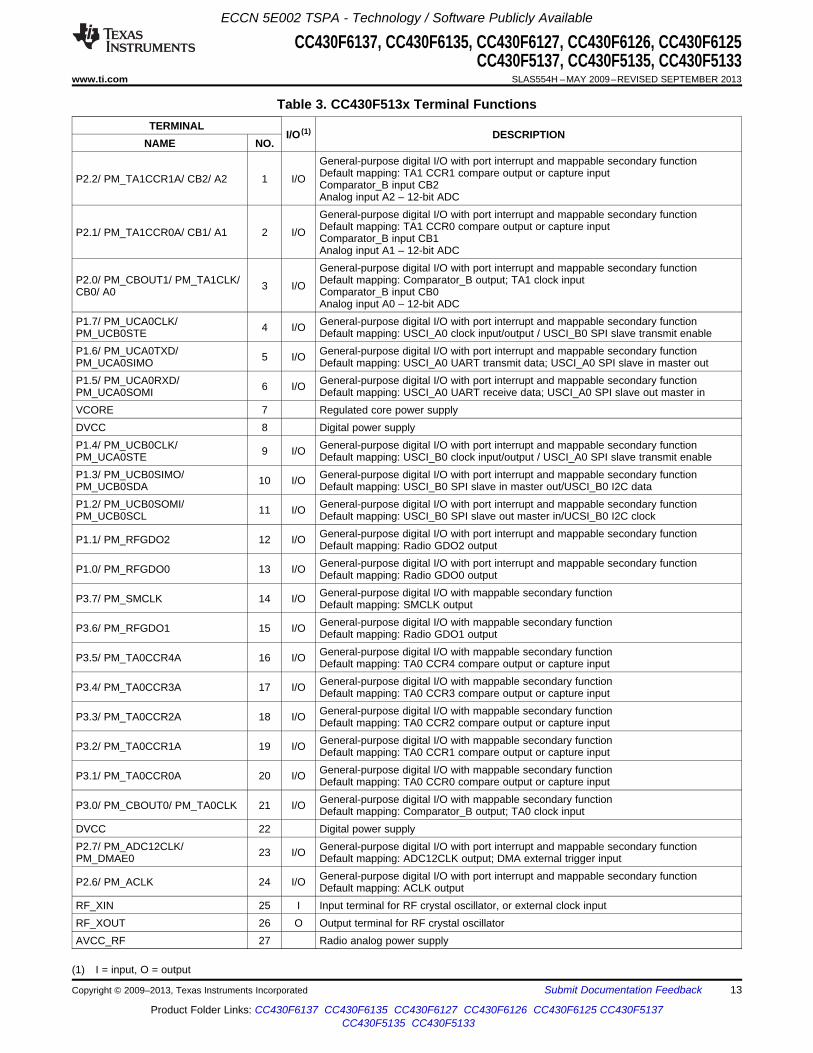
Table 3. CC430F513x Terminal FunctionsTERMINAL
I/O (1) DESCRIPTIONNAME NO.
General-purpose digital I/O with port interrupt and mappable secondary functionDefault mapping: TA1 CCR1 compare output or capture inputP2.2/ PM_TA1CCR1A/ CB2/ A2 1 I/O Comparator_B input CB2Analog input A2 – 12-bit ADCGeneral-purpose digital I/O with port interrupt and mappable secondary functionDefault mapping: TA1 CCR0 compare output or capture inputP2.1/ PM_TA1CCR0A/ CB1/ A1 2 I/O Comparator_B input CB1Analog input A1 – 12-bit ADCGeneral-purpose digital I/O with port interrupt and mappable secondary function
P2.0/ PM_CBOUT1/ PM_TA1CLK/ Default mapping: Comparator_B output; TA1 clock input3 I/OCB0/ A0 Comparator_B input CB0Analog input A0 – 12-bit ADC
P1.7/ PM_UCA0CLK/ General-purpose digital I/O with port interrupt and mappable secondary function4 I/OPM_UCB0STE Default mapping: USCI_A0 clock input/output / USCI_B0 SPI slave transmit enableP1.6/ PM_UCA0TXD/ General-purpose digital I/O with port interrupt and mappable secondary function5 I/OPM_UCA0SIMO Default mapping: USCI_A0 UART transmit data; USCI_A0 SPI slave in master outP1.5/ PM_UCA0RXD/ General-purpose digital I/O with port interrupt and mappable secondary function6 I/OPM_UCA0SOMI Default mapping: USCI_A0 UART receive data; USCI_A0 SPI slave out master inVCORE 7 Regulated core power supplyDVCC 8 Digital power supplyP1.4/ PM_UCB0CLK/ General-purpose digital I/O with port interrupt and mappable secondary function9 I/OPM_UCA0STE Default mapping: USCI_B0 clock input/output / USCI_A0 SPI slave transmit enableP1.3/ PM_UCB0SIMO/ General-purpose digital I/O with port interrupt and mappable secondary function10 I/OPM_UCB0SDA Default mapping: USCI_B0 SPI slave in master out/USCI_B0 I2C dataP1.2/ PM_UCB0SOMI/ General-purpose digital I/O with port interrupt and mappable secondary function11 I/OPM_UCB0SCL Default mapping: USCI_B0 SPI slave out master in/UCSI_B0 I2C clock
General-purpose digital I/O with port interrupt and mappable secondary functionP1.1/ PM_RFGDO2 12 I/O Default mapping: Radio GDO2 outputGeneral-purpose digital I/O with port interrupt and mappable secondary functionP1.0/ PM_RFGDO0 13 I/O Default mapping: Radio GDO0 outputGeneral-purpose digital I/O with mappable secondary functionP3.7/ PM_SMCLK 14 I/O Default mapping: SMCLK outputGeneral-purpose digital I/O with mappable secondary functionP3.6/ PM_RFGDO1 15 I/O Default mapping: Radio GDO1 outputGeneral-purpose digital I/O with mappable secondary functionP3.5/ PM_TA0CCR4A 16 I/O Default mapping: TA0 CCR4 compare output or capture inputGeneral-purpose digital I/O with mappable secondary functionP3.4/ PM_TA0CCR3A 17 I/O Default mapping: TA0 CCR3 compare output or capture inputGeneral-purpose digital I/O with mappable secondary functionP3.3/ PM_TA0CCR2A 18 I/O Default mapping: TA0 CCR2 compare output or capture inputGeneral-purpose digital I/O with mappable secondary functionP3.2/ PM_TA0CCR1A 19 I/O Default mapping: TA0 CCR1 compare output or capture inputGeneral-purpose digital I/O with mappable secondary functionP3.1/ PM_TA0CCR0A 20 I/O Default mapping: TA0 CCR0 compare output or capture inputGeneral-purpose digital I/O with mappable secondary functionP3.0/ PM_CBOUT0/ PM_TA0CLK 21 I/O Default mapping: Comparator_B output; TA0 clock input
DVCC 22 Digital power supplyP2.7/ PM_ADC12CLK/ General-purpose digital I/O with port interrupt and mappable secondary function23 I/OPM_DMAE0 Default mapping: ADC12CLK output; DMA external trigger input
General-purpose digital I/O with port interrupt and mappable secondary functionP2.6/ PM_ACLK 24 I/O Default mapping: ACLK outputRF_XIN 25 I Input terminal for RF crystal oscillator, or external clock inputRF_XOUT 26 O Output terminal for RF crystal oscillatorAVCC_RF 27 Radio analog power supply
(1) I = input, O = output
Copyright © 2009–2013, Texas Instruments Incorporated Submit Documentation Feedback 13
Product Folder Links: CC430F6137 CC430F6135 CC430F6127 CC430F6126 CC430F6125 CC430F5137CC430F5135 CC430F5133

ECCN 5E002 TSPA - Technology / Software Publicly Available
CC430F6137, CC430F6135, CC430F6127, CC430F6126, CC430F6125CC430F5137, CC430F5135, CC430F5133SLAS554H –MAY 2009–REVISED SEPTEMBER 2013 www.ti.com
Table 3. CC430F513x Terminal Functions (continued)TERMINAL
I/O (1) DESCRIPTIONNAME NO.
AVCC_RF 28 Radio analog power supplyRF Positive RF input to LNA in receive modeRF_P 29 I/O Positive RF output from PA in transmit modeRF Negative RF input to LNA in receive modeRF_N 30 I/O Negative RF output from PA in transmit mode
AVCC_RF 31 Radio analog power supplyAVCC_RF 32 Radio analog power supplyRBIAS 33 External bias resistor for radio reference currentGUARD 34 Power supply connection for digital noise isolation
General-purpose digital I/OPJ.0/ TDO 35 I/O Test data output portGeneral-purpose digital I/OPJ.1/ TDI/ TCLK 36 I/O Test data input or test clock inputGeneral-purpose digital I/OPJ.2/ TMS 37 I/O Test mode selectGeneral-purpose digital I/OPJ.3/ TCK 38 I/O Test clockTest mode pin – select digital I/O on JTAG pinsTEST/ SBWTCK 39 I Spy-Bi-Wire input clockReset input active low
RST/NMI/ SBWTDIO 40 I/O Non-maskable interrupt inputSpy-Bi-Wire data input/output
DVCC 41 Digital power supplyAVSS 42 Analog ground supply for ADC12
General-purpose digital I/OP5.1/ XOUT 43 I/O Output terminal of crystal oscillator XT1General-purpose digital I/OP5.0/ XIN 44 I/O Input terminal for crystal oscillator XT1
AVCC 45 Analog power supplyGeneral-purpose digital I/O with port interrupt and mappable secondary functionDefault mapping: SVM output
P2.5/ PM_SVMOUT/ CB5/ Comparator_B input CB546 I/OA5/ VREF+/ VeREF+ Analog input A5 – 12-bit ADCOutput of reference voltage to the ADCInput for an external reference voltage to the ADCGeneral-purpose digital I/O with port interrupt and mappable secondary functionDefault mapping: RTCCLK output
P2.4/ PM_RTCCLK/ CB4/ Comparator_B input CB447 I/OA4/ VREF-/ VeREF- Analog input A4 – 12-bit ADCNegative terminal for the ADC's reference voltage for both sources, the internalreference voltage, or an external applied reference voltageGeneral-purpose digital I/O with port interrupt and mappable secondary functionDefault mapping: TA1 CCR2 compare output or capture inputP2.3/ PM_TA1CCR2A/ CB3/ A3 48 I/O Comparator_B input CB3Analog input A3 – 12-bit ADCGround supply
VSS - Exposed die attach pad The exposed die attach pad must be connected to a solid ground plane as this isthe ground connection for the chip.
14 Submit Documentation Feedback Copyright © 2009–2013, Texas Instruments Incorporated
Product Folder Links: CC430F6137 CC430F6135 CC430F6127 CC430F6126 CC430F6125 CC430F5137CC430F5135 CC430F5133

BIAS
PA
RBIAS RF_XIN RF_XOUT
XOSC
LNA
0
90
FREQ
SYNTH
ADC
DE
MO
DU
LA
TO
R
PA
CK
ET
HA
ND
LE
R
RX
FIF
OT
XF
IFO
INT
ER
FA
CE
TO
MC
U
RADIO CONTROL
RF_P
RF_N
RC OSC
ADC
MO
DU
LA
TO
R
ECCN 5E002 TSPA - Technology / Software Publicly Available
CC430F6137, CC430F6135, CC430F6127, CC430F6126, CC430F6125CC430F5137, CC430F5135, CC430F5133
www.ti.com SLAS554H –MAY 2009–REVISED SEPTEMBER 2013
Short-Form Description
Sub-1-GHz RadioThe implemented sub-1-GHz radio module is based on the industry-leading CC1101, requiring very few externalcomponents. Figure 1 shows a high-level block diagram of the implemented radio.
Figure 1. Sub-1-GHz Radio Block Diagram
The radio features a low-IF receiver. The received RF signal is amplified by a low-noise amplifier (LNA) anddown-converted in quadrature to the intermediate frequency (IF). At IF, the I/Q signals are digitized. Automaticgain control (AGC), fine channel filtering, demodulation bit and packet synchronization are performed digitally.
The transmitter part is based on direct synthesis of the RF frequency. The frequency synthesizer includes acompletely on-chip LC VCO and a 90° phase shifter for generating the I and Q LO signals to the down-conversion mixers in receive mode.
The 26-MHz crystal oscillator generates the reference frequency for the synthesizer, as well as clocks for theADC and the digital part.
A memory mapped register interface is used for data access, configuration, and status request by the CPU.
The digital baseband includes support for channel configuration, packet handling, and data buffering.
For complete module descriptions, see the CC430 Family User's Guide (SLAU259).
Copyright © 2009–2013, Texas Instruments Incorporated Submit Documentation Feedback 15
Product Folder Links: CC430F6137 CC430F6135 CC430F6127 CC430F6126 CC430F6125 CC430F5137CC430F5135 CC430F5133

ECCN 5E002 TSPA - Technology / Software Publicly Available
CC430F6137, CC430F6135, CC430F6127, CC430F6126, CC430F6125CC430F5137, CC430F5135, CC430F5133SLAS554H –MAY 2009–REVISED SEPTEMBER 2013 www.ti.com
CPUThe MSP430 CPU has a 16-bit RISC architecture that is highly transparent to the application. All operations,other than program-flow instructions, are performed as register operations in conjunction with seven addressingmodes for source operand and four addressing modes for destination operand.
The CPU is integrated with 16 registers that provide reduced instruction execution time. The register-to-registeroperation execution time is one cycle of the CPU clock.
Four of the registers, R0 to R3, are dedicated as program counter, stack pointer, status register, and constantgenerator, respectively. The remaining registers are general-purpose registers.
Peripherals are connected to the CPU using data, address, and control buses and can be handled with allinstructions.
The instruction set consists of the original 51 instructions with three formats and seven address modes andadditional instructions for the expanded address range. Each instruction can operate on word and byte data.
Operating ModesThe CC430 has one active mode and five software-selectable low-power modes of operation. An interrupt eventcan wake up the device from any of the low-power modes, service the request, and restore back to the low-power mode on return from the interrupt program.
The following six operating modes can be configured by software:• Active mode (AM)
– All clocks are active• Low-power mode 0 (LPM0)
– CPU is disabled– ACLK and SMCLK remain active, MCLK is disabled– FLL loop control remains active
• Low-power mode 1 (LPM1)– CPU is disabled– FLL loop control is disabled– ACLK and SMCLK remain active, MCLK is disabled
• Low-power mode 2 (LPM2)– CPU is disabled– MCLK and FLL loop control and DCOCLK are disabled– DCO's dc-generator remains enabled– ACLK remains active
• Low-power mode 3 (LPM3)– CPU is disabled– MCLK, FLL loop control, and DCOCLK are disabled– DCO's dc-generator is disabled– ACLK remains active
• Low-power mode 4 (LPM4)– CPU is disabled– ACLK is disabled– MCLK, FLL loop control, and DCOCLK are disabled– DCO's dc-generator is disabled– Crystal oscillator is stopped– Complete data retention
16 Submit Documentation Feedback Copyright © 2009–2013, Texas Instruments Incorporated
Product Folder Links: CC430F6137 CC430F6135 CC430F6127 CC430F6126 CC430F6125 CC430F5137CC430F5135 CC430F5133

ECCN 5E002 TSPA - Technology / Software Publicly Available
CC430F6137, CC430F6135, CC430F6127, CC430F6126, CC430F6125CC430F5137, CC430F5135, CC430F5133
www.ti.com SLAS554H –MAY 2009–REVISED SEPTEMBER 2013
Interrupt Vector AddressesThe interrupt vectors and the power-up start address are located in the address range 0FFFFh to 0FF80h. Thevector contains the 16-bit address of the appropriate interrupt-handler instruction sequence.
Table 4. Interrupt Sources, Flags, and VectorsSYSTEM WORDINTERRUPT SOURCE INTERRUPT FLAG PRIORITYINTERRUPT ADDRESS
System ResetPower-Up
External Reset WDTIFG, KEYV (SYSRSTIV) (1) (2) Reset 0FFFEh 63, highestWatchdog Timeout, PasswordViolation
Flash Memory Password ViolationSystem NMI SVMLIFG, SVMHIFG, DLYLIFG, DLYHIFG,PMM VLRLIFG, VLRHIFG, VMAIFG, JMBNIFG, (Non)maskable 0FFFCh 62Vacant Memory Access JMBOUTIFG (SYSSNIV) (1) (3)
JTAG MailboxUser NMI
NMI NMIIFG, OFIFG, ACCVIFG (SYSUNIV) (1) (3) (Non)maskable 0FFFAh 61Oscillator FaultFlash Memory Access Violation
Comparator_B Comparator_B Interrupt Flags (CBIV) (1) Maskable 0FFF8h 60Watchdog Interval Timer Mode WDTIFG Maskable 0FFF6h 59USCI_A0 Receive or Transmit UCA0RXIFG, UCA0TXIFG (UCA0IV) (1) Maskable 0FFF4h 58
UCB0RXIFG, UCB0TXIFG, I2C Status InterruptUSCI_B0 Receive or Transmit Maskable 0FFF2h 57Flags (UCB0IV) (1)
ADC12_A ADC12IFG0 ... ADC12IFG15 (ADC12IV) (1) Maskable 0FFF0h 56(Reserved on CC430F612x)TA0 TA0CCR0 CCIFG0 Maskable 0FFEEh 55
TA0CCR1 CCIFG1 ... TA0CCR4 CCIFG4,TA0 Maskable 0FFECh 54TA0IFG (TA0IV) (1)
Radio Interface Interrupt Flags (RF1AIFIV)RF1A CC1101-based Radio Maskable 0FFEAh 53Radio Core Interrupt Flags (RF1AIV)DMA DMA0IFG, DMA1IFG, DMA2IFG (DMAIV) (1) Maskable 0FFE8h 52TA1 TA1CCR0 CCIFG0 Maskable 0FFE6h 51
TA1CCR1 CCIFG1 ... TA1CCR2 CCIFG2,TA1 Maskable 0FFE4h 50TA1IFG (TA1IV) (1)
I/O Port P1 P1IFG.0 to P1IFG.7 (P1IV) (1) Maskable 0FFE2h 49I/O Port P2 P2IFG.0 to P2IFG.7 (P2IV) (1) Maskable 0FFE0h 48
LCD_B LCD_B Interrupt Flags (LCDBIV) (1) Maskable 0FFDEh 47(Reserved on CC430F513x)RTCRDYIFG, RTCTEVIFG, RTCAIFG,RTC_A Maskable 0FFDCh 46RT0PSIFG, RT1PSIFG (RTCIV) (1)
AES AESRDYIFG Maskable 0FFDAh 450FFD8h 44
Reserved Reserved (4) ⋮ ⋮0FF80h 0, lowest
(1) Multiple source flags(2) A reset is generated if the CPU tries to fetch instructions from within peripheral space.(3) (Non)maskable: the individual interrupt-enable bit can disable an interrupt event, but the general-interrupt enable cannot disable it.(4) Reserved interrupt vectors at addresses are not used in this device and can be used for regular program code if necessary. To maintain
compatibility with other devices, it is recommended to reserve these locations.
Copyright © 2009–2013, Texas Instruments Incorporated Submit Documentation Feedback 17
Product Folder Links: CC430F6137 CC430F6135 CC430F6127 CC430F6126 CC430F6125 CC430F5137CC430F5135 CC430F5133

ECCN 5E002 TSPA - Technology / Software Publicly Available
CC430F6137, CC430F6135, CC430F6127, CC430F6126, CC430F6125CC430F5137, CC430F5135, CC430F5133SLAS554H –MAY 2009–REVISED SEPTEMBER 2013 www.ti.com
Memory Organization
Table 5. Memory OrganizationCC430F6137 CC430F6135CC430F6127 CC430F6126 (1) CC430F6125 CC430F5133 (1)
CC430F5137 (1) CC430F5135 (1)
Main Memory Total 32kB 32kB 16kB 8kB(flash) SizeMain: Interrupt 00FFFFh to 00FF80h 00FFFFh to 00FF80h 00FFFFh to 00FF80h 00FFFFh to 00FF80hvectorMain: code Bank 0 32kB 32kB 16kB 8kBmemory 00FFFFh to 008000h 00FFFFh to 008000h 00FFFFh to 00C000h 00FFFFh to 00E000h
Total 4kB 2kB 2kB 2kBRAM SizeSect 1 2kB not available not available not available
002BFFh to 002400hSect 0 2kB 2kB 2kB 2kB
0023FFh to 001C00h 0023FFh to 001C00h 0023FFh to 001C00h 0023FFh to 001C00h128 B 128 B 128 B 128 B
001AFFh to 001A80h 001AFFh to 001A80h 001AFFh to 001A80h 001AFFh to 001A80hDeviceDescriptor 128 B 128 B 128 B 128 B
001A7Fh to 001A00h 001A7Fh to 001A00h 001A7Fh to 001A00h 001A7Fh to 001A00hInfo A 128 B 128 B 128 B 128 B
0019FFh to 001980h 0019FFh to 001980h 0019FFh to 001980h 0019FFh to 001980hInfo B 128 B 128 B 128 B 128 B
00197Fh to 001900h 00197Fh to 001900h 00197Fh to 001900h 00197Fh to 001900hInformationmemory (flash) Info C 128 B 128 B 128 B 128 B
0018FFh to 001880h 0018FFh to 001880h 0018FFh to 001880h 0018FFh to 001880hInfo D 128 B 128 B 128 B 128 B
00187Fh to 001800h 00187Fh to 001800h 00187Fh to 001800h 00187Fh to 001800hBSL 3 512 B 512 B 512 B 512 B
0017FFh to 001600h 0017FFh to 001600h 0017FFh to 001600h 0017FFh to 001600hBSL 2 512 B 512 B 512 B 512 B
Bootstrap loader 0015FFh to 001400h 0015FFh to 001400h 0015FFh to 001400h 0015FFh to 001400h(BSL) memory
BSL 1 512 B 512 B 512 B 512 B(flash)0013FFh to 001200h 0013FFh to 001200h 0013FFh to 001200h 0013FFh to 001200h
BSL 0 512 B 512 B 512 B 512 B0011FFh to 001000h 0011FFh to 001000h 0011FFh to 001000h 0011FFh to 001000h
4 KB 4 KB 4 KB 4 KBPeripherals 000FFFh to 0h 000FFFh to 0h 000FFFh to 0h 000FFFh to 0h
(1) All memory regions not specified here are vacant memory, and any access to them causes a Vacant Memory Interrupt.
Bootstrap Loader (BSL)The BSL enables users to program the flash memory or RAM using various serial interfaces. Access to thedevice memory via the BSL is protected by an user-defined password. BSL entry requires a specific entrysequence on the RST/NMI/SBWTDIO and TEST/SBWTCK pins. For a complete description of the features of theBSL and its implementation, see the MSP430 Programming Via the Bootstrap Loader User's Guide (SLAU319).
Table 6. UART BSL Pin Requirements and FunctionsDEVICE SIGNAL BSL FUNCTION
RST/NMI/SBWTDIO Entry sequence signalTEST/SBWTCK Entry sequence signal
P1.6 Data transmitP1.5 Data receiveVCC Power supplyVSS Ground supply
18 Submit Documentation Feedback Copyright © 2009–2013, Texas Instruments Incorporated
Product Folder Links: CC430F6137 CC430F6135 CC430F6127 CC430F6126 CC430F6125 CC430F5137CC430F5135 CC430F5133

ECCN 5E002 TSPA - Technology / Software Publicly Available
CC430F6137, CC430F6135, CC430F6127, CC430F6126, CC430F6125CC430F5137, CC430F5135, CC430F5133
www.ti.com SLAS554H –MAY 2009–REVISED SEPTEMBER 2013
JTAG Operation
JTAG Standard InterfaceThe CC430 family supports the standard JTAG interface which requires four signals for sending and receivingdata. The JTAG signals are shared with general-purpose I/O. The TEST/SBWTCK pin is used to enable theJTAG signals. In addition to these signals, the RST/NMI/SBWTDIO is required to interface with MSP430development tools and device programmers. The JTAG pin requirements are shown in Table 7. For furtherdetails on interfacing to development tools and device programmers, see the MSP430 Hardware Tools User'sGuide (SLAU278). For a complete description of the features of the JTAG interface and its implementation, seeMSP430 Programming Via the JTAG Interface (SLAU320).
Table 7. JTAG Pin Requirements and FunctionsDEVICE SIGNAL DIRECTION FUNCTION
PJ.3/TCK IN JTAG clock inputPJ.2/TMS IN JTAG state control
PJ.1/TDI/TCLK IN JTAG data input, TCLK inputPJ.0/TDO OUT JTAG data output
TEST/SBWTCK IN Enable JTAG pinsRST/NMI/SBWTDIO IN External reset
VCC Power supplyVSS Ground supply
Spy-Bi-Wire InterfaceIn addition to the standard JTAG interface, the CC430 family supports the two wire Spy-Bi-Wire interface. Spy-Bi-Wire can be used to interface with MSP430 development tools and device programmers. The Spy-Bi-Wireinterface pin requirements are shown in Table 8. For further details on interfacing to development tools anddevice programmers, see the MSP430 Hardware Tools User's Guide (SLAU278). For a complete description ofthe features of the JTAG interface and its implementation, see MSP430 Programming Via the JTAG Interface(SLAU320).
Table 8. Spy-Bi-Wire Pin Requirements and FunctionsDEVICE SIGNAL DIRECTION FUNCTIONTEST/SBWTCK IN Spy-Bi-Wire clock input
RST/NMI/SBWTDIO IN, OUT Spy-Bi-Wire data input/outputVCC Power supplyVSS Ground supply
Flash MemoryThe flash memory can be programmed via the JTAG port, Spy-Bi-Wire (SBW), or in-system by the CPU. TheCPU can perform single-byte, single-word, and long-word writes to the flash memory. Features of the flashmemory include:• Flash memory has n segments of main memory and four segments of information memory (Info A to Info D)
of 128 bytes each. Each segment in main memory is 512 bytes in size.• Segments 0 to n may be erased in one step, or each segment may be individually erased.• Segments Info A to Info D can be erased individually, or as a group with the main memory segments.
Segments Info A to Info D are also called information memory.• Segment A can be locked separately.
Copyright © 2009–2013, Texas Instruments Incorporated Submit Documentation Feedback 19
Product Folder Links: CC430F6137 CC430F6135 CC430F6127 CC430F6126 CC430F6125 CC430F5137CC430F5135 CC430F5133

ECCN 5E002 TSPA - Technology / Software Publicly Available
CC430F6137, CC430F6135, CC430F6127, CC430F6126, CC430F6125CC430F5137, CC430F5135, CC430F5133SLAS554H –MAY 2009–REVISED SEPTEMBER 2013 www.ti.com
RAM MemoryThe RAM memory is made up of n sectors. Each sector can be completely powered down to save leakage,however, all data is lost. Features of the RAM memory include:• RAM memory has n sectors of 2k bytes each.• Each sector 0 to n can be complete disabled, however data retention is lost.• Each sector 0 to n automatically enters low power retention mode when possible.
PeripheralsPeripherals are connected to the CPU through data, address, and control busses and can be handled using allinstructions. For complete module descriptions, see the CC430 Family User's Guide (SLAU259).
Oscillator and System ClockThe Unified Clock System (UCS) module includes support for a 32768-Hz watch crystal oscillator, an internalvery-low-power low-frequency oscillator (VLO), an internal trimmed low-frequency oscillator (REFO), anintegrated internal digitally-controlled oscillator (DCO), and a high-frequency crystal oscillator. The UCS moduleis designed to meet the requirements of both low system cost and low-power consumption. The UCS modulefeatures digital frequency locked loop (FLL) hardware that, in conjunction with a digital modulator, stabilizes theDCO frequency to a programmable multiple of the watch crystal frequency. The internal DCO provides a fastturn-on clock source and stabilizes in less than 5 µs. The UCS module provides the following clock signals:• Auxiliary clock (ACLK), sourced from a 32768-Hz watch crystal, a high-frequency crystal, the internal low-
frequency oscillator (VLO), or the trimmed low-frequency oscillator (REFO).• Main clock (MCLK), the system clock used by the CPU. MCLK can be sourced by same sources made
available to ACLK.• Sub-Main clock (SMCLK), the subsystem clock used by the peripheral modules. SMCLK can be sourced by
same sources made available to ACLK.• ACLK/n, the buffered output of ACLK, ACLK/2, ACLK/4, ACLK/8, ACLK/16, ACLK/32.
Power Management Module (PMM)The PMM includes an integrated voltage regulator that supplies the core voltage to the device and containsprogrammable output levels to provide for power optimization. The PMM also includes supply voltage supervisor(SVS) and supply voltage monitoring (SVM) circuitry, as well as brownout protection. The brownout circuit isimplemented to provide the proper internal reset signal to the device during power-on and power-off. TheSVS/SVM circuitry detects if the supply voltage drops below a user-selectable level and supports both supplyvoltage supervision (the device is automatically reset) and supply voltage monitoring (SVM, the device is notautomatically reset). SVS and SVM circuitry is available on the primary supply and core supply.
Digital I/OThere are up to five 8-bit I/O ports implemented: ports P1 through P5.• All individual I/O bits are independently programmable.• Any combination of input, output, and interrupt conditions is possible.• Programmable pullup or pulldown on all ports.• Programmable drive strength on all ports.• Edge-selectable interrupt input capability for all the eight bits of ports P1 and P2.• Read/write access to port-control registers is supported by all instructions.• Ports can be accessed byte-wise (P1 through P5) or word-wise in pairs (PA and PB).
20 Submit Documentation Feedback Copyright © 2009–2013, Texas Instruments Incorporated
Product Folder Links: CC430F6137 CC430F6135 CC430F6127 CC430F6126 CC430F6125 CC430F5137CC430F5135 CC430F5133

ECCN 5E002 TSPA - Technology / Software Publicly Available
CC430F6137, CC430F6135, CC430F6127, CC430F6126, CC430F6125CC430F5137, CC430F5135, CC430F5133
www.ti.com SLAS554H –MAY 2009–REVISED SEPTEMBER 2013
Port Mapping ControllerThe port mapping controller allows the flexible and re-configurable mapping of digital functions to port pins ofports P1 through P3.
Table 9. Port Mapping, Mnemonics and FunctionsOUTPUT PIN FUNCTIONVALUE PxMAPy MNEMONIC INPUT PIN FUNCTION (PxDIR.y = 0) (PxDIR.y = 1)
0 PM_NONE None DVSSComparator_B output (on TA0 clockPM_CBOUT0 input)1 (1)
PM_TA0CLK TA0 clock input -Comparator_B output (on TA1 clockPM_CBOUT1 - input)2 (1)
PM_TA1CLK TA1 clock input -3 PM_ACLK None ACLK output4 PM_MCLK None MCLK output5 PM_SMCLK None SMCLK output6 PM_RTCCLK None RTCCLK output
PM_ADC12CLK - ADC12CLK output7 (1)
PM_DMAE0 DMA external trigger input -8 PM_SVMOUT None SVM output9 PM_TA0CCR0A TA0 CCR0 capture input CCI0A TA0 CCR0 compare output Out0
10 PM_TA0CCR1A TA0 CCR1 capture input CCI1A TA0 CCR1 compare output Out111 PM_TA0CCR2A TA0 CCR2 capture input CCI2A TA0 CCR2 compare output Out212 PM_TA0CCR3A TA0 CCR3 capture input CCI3A TA0 CCR3 compare output Out313 PM_TA0CCR4A TA0 CCR4 capture input CCI4A TA0 CCR4 compare output Out414 PM_TA1CCR0A TA1 CCR0 capture input CCI0A TA1 CCR0 compare output Out015 PM_TA1CCR1A TA1 CCR1 capture input CCI1A TA1 CCR1 compare output Out116 PM_TA1CCR2A TA1 CCR2 capture input CCI2A TA1 CCR2 compare output Out2
PM_UCA0RXD USCI_A0 UART RXD (Direction controlled by USCI - input)17 (2)
PM_UCA0SOMI USCI_A0 SPI slave out master in (direction controlled by USCI)PM_UCA0TXD USCI_A0 UART TXD (Direction controlled by USCI - output)
18 (2)PM_UCA0SIMO USCI_A0 SPI slave in master out (direction controlled by USCI)PM_UCA0CLK USCI_A0 clock input/output (direction controlled by USCI)
19 (3)PM_UCB0STE USCI_B0 SPI slave transmit enable (direction controlled by USCI - input)
PM_UCB0SOMI USCI_B0 SPI slave out master in (direction controlled by USCI)20 (4)
PM_UCB0SCL USCI_B0 I2C clock (open drain and direction controlled by USCI)PM_UCB0SIMO USCI_B0 SPI slave in master out (direction controlled by USCI)
21 (4)PM_UCB0SDA USCI_B0 I2C data (open drain and direction controlled by USCI)PM_UCB0CLK USCI_B0 clock input/output (direction controlled by USCI)
22 (5)PM_UCA0STE USCI_A0 SPI slave transmit enable (direction controlled by USCI - input)
23 PM_RFGDO0 Radio GDO0 (direction controlled by Radio)24 PM_RFGDO1 Radio GDO1 (direction controlled by Radio)25 PM_RFGDO2 Radio GDO2 (direction controlled by Radio)26 Reserved None DVSS
(1) Input or output function is selected by the corresponding setting in the port direction register PxDIR.(2) UART or SPI functionality is determined by the selected USCI mode.(3) UCA0CLK function takes precedence over UCB0STE function. If the mapped pin is required as UCA0CLK input or output USCI_B0 will
be forced to 3-wire SPI mode even if 4-wire mode is selected.(4) SPI or I2C functionality is determined by the selected USCI mode. In case the I2C functionality is selected the output of the mapped pin
drives only the logical 0 to VSS level.(5) UCB0CLK function takes precedence over UCA0STE function. If the mapped pin is required as UCB0CLK input or output USCI_A0 will
be forced to 3-wire SPI mode even if 4-wire mode is selected.
Copyright © 2009–2013, Texas Instruments Incorporated Submit Documentation Feedback 21
Product Folder Links: CC430F6137 CC430F6135 CC430F6127 CC430F6126 CC430F6125 CC430F5137CC430F5135 CC430F5133

ECCN 5E002 TSPA - Technology / Software Publicly Available
CC430F6137, CC430F6135, CC430F6127, CC430F6126, CC430F6125CC430F5137, CC430F5135, CC430F5133SLAS554H –MAY 2009–REVISED SEPTEMBER 2013 www.ti.com
Table 9. Port Mapping, Mnemonics and Functions (continued)OUTPUT PIN FUNCTIONVALUE PxMAPy MNEMONIC INPUT PIN FUNCTION (PxDIR.y = 0) (PxDIR.y = 1)
27 Reserved None DVSS28 Reserved None DVSS29 Reserved None DVSS30 Reserved None DVSS
Disables the output driver as well as the input Schmitt-trigger to prevent31 (0FFh) (6) PM_ANALOG parasitic cross currents when applying analog signals.
(6) The value of the PM_ANALOG mnemonic is set to 0FFh. The port mapping registers are only 5 bits wide and the upper bits are ignoredresulting in a read out value of 31.
Table 10. Default MappingINPUT PIN FUNCTION OUTPUT PIN FUNCTIONPIN PxMAPy MNEMONIC (PxDIR.y = 0) (PxDIR.y = 1)
P1.0/P1MAP0 PM_RFGDO0 None Radio GDO0P1.1/P1MAP1 PM_RFGDO2 None Radio GDO2
USCI_B0 SPI slave out master in (direction controlled by USCI),P1.2/P1MAP2 PM_UCB0SOMI/PM_UCB0SCL USCI_B0 I2C clock (open drain and direction controlled by USCI)USCI_B0 SPI slave in master out (direction controlled by USCI),P1.3/P1MAP3 PM_UCB0SIMO/PM_UCB0SDA USCI_B0 I2C data (open drain and direction controlled by USCI)
USCI_B0 clock input/output (direction controlled by USCI),P1.4/P1MAP4 PM_UCB0CLK/PM_UCA0STE USCI_A0 SPI slave transmit enable (direction controlled by USCI - input)USCI_A0 UART RXD (Direction controlled by USCI - input),P1.5/P1MAP5 PM_UCA0RXD/PM_UCA0SOMI USCI_A0 SPI slave out master in (direction controlled by USCI)USCI_A0 UART TXD (Direction controlled by USCI - output),P1.6/P1MAP6 PM_UCA0TXD/PM_UCA0SIMO USCI_A0 SPI slave in master out (direction controlled by USCI)USCI_A0 clock input/output (direction controlled by USCI),P1.7/P1MAP7 PM_UCA0CLK/PM_UCB0STE USCI_B0 SPI slave transmit enable (direction controlled by USCI - input)
P2.0/P2MAP0 PM_CBOUT1/PM_TA1CLK TA1 clock input Comparator_B outputP2.1/P2MAP1 PM_TA1CCR0A TA1 CCR0 capture input CCI0A TA1 CCR0 compare output Out0P2.2/P2MAP2 PM_TA1CCR1A TA1 CCR1 capture input CCI1A TA1 CCR1 compare output Out1P2.3/P2MAP3 PM_TA1CCR2A TA1 CCR2 capture input CCI2A TA1 CCR2 compare output Out2P2.4/P2MAP4 PM_RTCCLK None RTCCLK outputP2.5/P2MAP5 PM_SVMOUT None SVM outputP2.6/P2MAP6 PM_ACLK None ACLK outputP2.7/P2MAP7 PM_ADC12CLK/PM_DMAE0 DMA external trigger input ADC12CLK outputP3.0/P3MAP0 PM_CBOUT0/PM_TA0CLK TA0 clock input Comparator_B outputP3.1/P3MAP1 PM_TA0CCR0A TA0 CCR0 capture input CCI0A TA0 CCR0 compare output Out0P3.2/P3MAP2 PM_TA0CCR1A TA0 CCR1 capture input CCI1A TA0 CCR1 compare output Out1P3.3/P3MAP3 PM_TA0CCR2A TA0 CCR2 capture input CCI2A TA0 CCR2 compare output Out2P3.4/P3MAP4 PM_TA0CCR3A TA0 CCR3 capture input CCI3A TA0 CCR3 compare output Out3P3.5/P3MAP5 PM_TA0CCR4A TA0 CCR4 capture input CCI4A TA0 CCR4 compare output Out4P3.6/P3MAP6 PM_RFGDO1 None Radio GDO1P3.7/P3MAP7 PM_SMCLK None SMCLK output
22 Submit Documentation Feedback Copyright © 2009–2013, Texas Instruments Incorporated
Product Folder Links: CC430F6137 CC430F6135 CC430F6127 CC430F6126 CC430F6125 CC430F5137CC430F5135 CC430F5133

ECCN 5E002 TSPA - Technology / Software Publicly Available
CC430F6137, CC430F6135, CC430F6127, CC430F6126, CC430F6125CC430F5137, CC430F5135, CC430F5133
www.ti.com SLAS554H –MAY 2009–REVISED SEPTEMBER 2013
System Module (SYS)The SYS module handles many of the system functions within the device. These include power on reset andpower up clear handling, NMI source selection and management, reset interrupt vector generators, boot straploader entry mechanisms, as well as, configuration management (device descriptors). It also includes a dataexchange mechanism via JTAG called a JTAG mailbox that can be used in the application.
Table 11. System Module Interrupt Vector RegistersINTERRUPT VECTOR REGISTER ADDRESS INTERRUPT EVENT VALUE PRIORITY
SYSRSTIV, System Reset 019Eh No interrupt pending 00hBrownout (BOR) 02h HighestRST/NMI (POR) 04hDoBOR (BOR) 06h
Reserved 08hSecurity violation (BOR) 0Ah
SVSL (POR) 0ChSVSH (POR) 0Eh
SVML_OVP (POR) 10hSVMH_OVP (POR) 12h
DoPOR (POR) 14hWDT timeout (PUC) 16h
WDT password violation (PUC) 18hKEYV flash password violation (PUC) 1Ah
Reserved 1ChPeripheral area fetch (PUC) 1Eh
PMM password violation (PUC) 20hReserved 22h to 3Eh Lowest
SYSSNIV, System NMI 019Ch No interrupt pending 00hSVMLIFG 02h HighestSVMHIFG 04hDLYLIFG 06hDLYHIFG 08hVMAIFG 0Ah
JMBINIFG 0ChJMBOUTIFG 0Eh
VLRLIFG 10hVLRHIFG 12hReserved 14h to 1Eh Lowest
SYSUNIV, User NMI 019Ah No interrupt pending 00hNMIFG 02h HighestOFIFG 04h
ACCVIFG 06hReserved 08h to 1Eh Lowest
Copyright © 2009–2013, Texas Instruments Incorporated Submit Documentation Feedback 23
Product Folder Links: CC430F6137 CC430F6135 CC430F6127 CC430F6126 CC430F6125 CC430F5137CC430F5135 CC430F5133

ECCN 5E002 TSPA - Technology / Software Publicly Available
CC430F6137, CC430F6135, CC430F6127, CC430F6126, CC430F6125CC430F5137, CC430F5135, CC430F5133SLAS554H –MAY 2009–REVISED SEPTEMBER 2013 www.ti.com
DMA ControllerThe DMA controller allows movement of data from one memory address to another without CPU intervention.Using the DMA controller can increase the throughput of peripheral modules. The DMA controller reducessystem power consumption by allowing the CPU to remain in sleep mode, without having to awaken to movedata to or from a peripheral.
Table 12. DMA Trigger Assignments (1)
CHANNELTRIGGER
0 1 20 DMAREQ DMAREQ DMAREQ1 TA0CCR0 CCIFG TA0CCR0 CCIFG TA0CCR0 CCIFG2 TA0CCR2 CCIFG TA0CCR2 CCIFG TA0CCR2 CCIFG3 TA1CCR0 CCIFG TA1CCR0 CCIFG TA1CCR0 CCIFG4 TA1CCR2 CCIFG TA1CCR2 CCIFG TA1CCR2 CCIFG5 Reserved Reserved Reserved6 Reserved Reserved Reserved7 Reserved Reserved Reserved8 Reserved Reserved Reserved9 Reserved Reserved Reserved10 Reserved Reserved Reserved11 Reserved Reserved Reserved12 Reserved Reserved Reserved13 Reserved Reserved Reserved14 Reserved Reserved Reserved15 Reserved Reserved Reserved16 UCA0RXIFG UCA0RXIFG UCA0RXIFG17 UCA0TXIFG UCA0TXIFG UCA0TXIFG18 UCB0RXIFG UCB0RXIFG UCB0RXIFG19 UCB0TXIFG UCB0TXIFG UCB0TXIFG20 Reserved Reserved Reserved21 Reserved Reserved Reserved22 Reserved Reserved Reserved23 Reserved Reserved Reserved24 ADC12IFGx (2) ADC12IFGx (2) ADC12IFGx (2)
25 Reserved Reserved Reserved26 Reserved Reserved Reserved27 Reserved Reserved Reserved28 Reserved Reserved Reserved29 MPY ready MPY ready MPY ready30 DMA2IFG DMA0IFG DMA1IFG31 DMAE0 DMAE0 DMAE0
(1) Reserved DMA triggers may be used by other devices in the family. Reserved DMA triggers will notcause any DMA trigger event when selected.
(2) Only on CC430F613x and CC430F513x. Reserved on CC430F612x.
Watchdog Timer (WDT_A)The primary function of the watchdog timer is to perform a controlled system restart after a software problemoccurs. If the selected time interval expires, a system reset is generated. If the watchdog function is not neededin an application, the timer can be configured as an interval timer and can generate interrupts at selected timeintervals.
24 Submit Documentation Feedback Copyright © 2009–2013, Texas Instruments Incorporated
Product Folder Links: CC430F6137 CC430F6135 CC430F6127 CC430F6126 CC430F6125 CC430F5137CC430F5135 CC430F5133

ECCN 5E002 TSPA - Technology / Software Publicly Available
CC430F6137, CC430F6135, CC430F6127, CC430F6126, CC430F6125CC430F5137, CC430F5135, CC430F5133
www.ti.com SLAS554H –MAY 2009–REVISED SEPTEMBER 2013
CRC16The CRC16 module produces a signature based on a sequence of entered data values and can be used for datachecking purposes. The CRC16 module signature is based on the CRC-CCITT standard.
Hardware MultiplierThe multiplication operation is supported by a dedicated peripheral module. The module performs operations with32-bit, 24-bit, 16-bit, and 8-bit operands. The module is capable of supporting signed and unsigned multiplicationas well as signed and unsigned multiply and accumulate operations.
AES128 AcceleratorThe AES accelerator module performs encryption and decryption of 128-bit data with 128-bit keys according tothe Advanced Encryption Standard (AES) (FIPS PUB 197) in hardware.
Universal Serial Communication Interface (USCI)The USCI module is used for serial data communication. The USCI module supports synchronouscommunication protocols such as SPI (3 or 4 pin) and I2C, and asynchronous communication protocols such asUART, enhanced UART with automatic baudrate detection, and IrDA.
The USCI_An module provides support for SPI (3 or 4 pin), UART, enhanced UART, and IrDA.
The USCI_Bn module provides support for SPI (3 or 4 pin) and I2C.
A USCI_A0 and USCI_B0 module are implemented.
Copyright © 2009–2013, Texas Instruments Incorporated Submit Documentation Feedback 25
Product Folder Links: CC430F6137 CC430F6135 CC430F6127 CC430F6126 CC430F6125 CC430F5137CC430F5135 CC430F5133
ECCN 5E002 TSPA - Technology / Software Publicly Available
CC430F6137, CC430F6135, CC430F6127, CC430F6126, CC430F6125CC430F5137, CC430F5135, CC430F5133SLAS554H –MAY 2009–REVISED SEPTEMBER 2013 www.ti.com
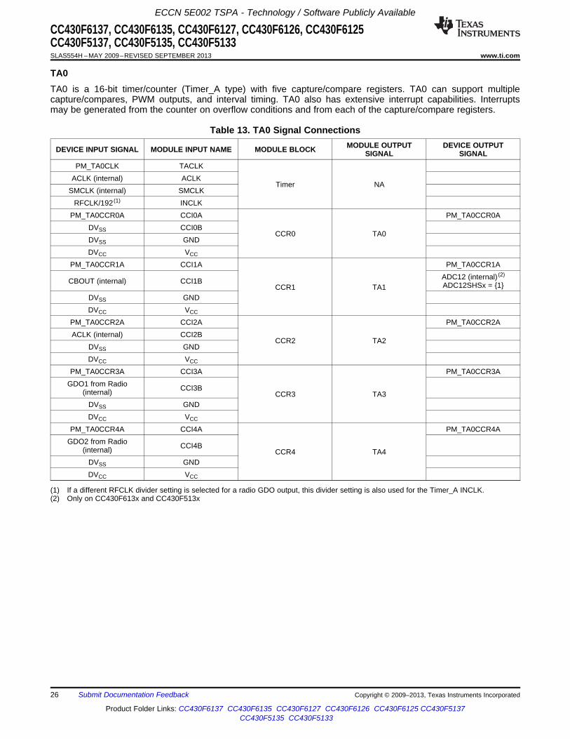
TA0TA0 is a 16-bit timer/counter (Timer_A type) with five capture/compare registers. TA0 can support multiplecapture/compares, PWM outputs, and interval timing. TA0 also has extensive interrupt capabilities. Interruptsmay be generated from the counter on overflow conditions and from each of the capture/compare registers.
Table 13. TA0 Signal ConnectionsMODULE OUTPUT DEVICE OUTPUTDEVICE INPUT SIGNAL MODULE INPUT NAME MODULE BLOCK SIGNAL SIGNAL
PM_TA0CLK TACLKACLK (internal) ACLK
Timer NASMCLK (internal) SMCLK
RFCLK/192 (1) INCLKPM_TA0CCR0A CCI0A PM_TA0CCR0A
DVSS CCI0BCCR0 TA0
DVSS GNDDVCC VCC
PM_TA0CCR1A CCI1A PM_TA0CCR1AADC12 (internal) (2)
CBOUT (internal) CCI1B ADC12SHSx = 1CCR1 TA1DVSS GNDDVCC VCC
PM_TA0CCR2A CCI2A PM_TA0CCR2AACLK (internal) CCI2B
CCR2 TA2DVSS GNDDVCC VCC
PM_TA0CCR3A CCI3A PM_TA0CCR3AGDO1 from Radio CCI3B(internal) CCR3 TA3
DVSS GNDDVCC VCC
PM_TA0CCR4A CCI4A PM_TA0CCR4AGDO2 from Radio CCI4B(internal) CCR4 TA4
DVSS GNDDVCC VCC
(1) If a different RFCLK divider setting is selected for a radio GDO output, this divider setting is also used for the Timer_A INCLK.(2) Only on CC430F613x and CC430F513x
26 Submit Documentation Feedback Copyright © 2009–2013, Texas Instruments Incorporated
Product Folder Links: CC430F6137 CC430F6135 CC430F6127 CC430F6126 CC430F6125 CC430F5137CC430F5135 CC430F5133

ECCN 5E002 TSPA - Technology / Software Publicly Available
CC430F6137, CC430F6135, CC430F6127, CC430F6126, CC430F6125CC430F5137, CC430F5135, CC430F5133
www.ti.com SLAS554H –MAY 2009–REVISED SEPTEMBER 2013
TA1TA1 is a 16-bit timer/counter (Timer_A type) with three capture/compare registers. TA1 can support multiplecapture/compares, PWM outputs, and interval timing. TA1 also has extensive interrupt capabilities. Interruptsmay be generated from the counter on overflow conditions and from each of the capture/compare registers.
Table 14. TA1 Signal ConnectionsDEVICE OUTPUT
MODULE OUTPUT SIGNALDEVICE INPUT SIGNAL MODULE INPUT NAME MODULE BLOCK SIGNALPZ
PM_TA1CLK TACLKACLK (internal) ACLK
Timer NASMCLK (internal) SMCLK
RFCLK/192 (1) INCLKPM_TA1CCR0A CCI0A PM_TA1CCR0A
RF Async. Output CCI0B RF Async. Input (internal)(internal) CCR0 TA0DVSS GNDDVCC VCC
PM_TA1CCR1A CCI1A PM_TA1CCR1ACBOUT (internal) CCI1B
CCR1 TA1DVSS GNDDVCC VCC
PM_TA1CCR2A CCI2A PM_TA1CCR2AACLK (internal) CCI2B
CCR2 TA2DVSS GNDDVCC VCC
(1) If a different RFCLK divider setting is selected for a radio GDO output, this divider setting is also used for the Timer_A INCLK.
Real-Time Clock (RTC_A)The RTC_A module can be used as a general-purpose 32-bit counter (counter mode) or as an integrated real-time clock (RTC) (calendar mode). In counter mode, the RTC_A also includes two independent 8-bit timers thatcan be cascaded to form a 16-bit timer/counter. Both timers can be read and written by software. Calendar modeintegrates an internal calendar which compensates for months with less than 31 days and includes leap yearcorrection. The RTC_A also supports flexible alarm functions and offset-calibration hardware.
REF Voltage ReferenceThe reference module (REF) is responsible for generation of all critical reference voltages that can be used bythe various analog peripherals in the device. These include the ADC12_A, LCD_B, and COMP_B modules.
LCD_B (Only CC430F613x and CC430F612x)The LCD_B driver generates the segment and common signals required to drive a liquid crystal display (LCD).The LCD_B controller has dedicated data memories to hold segment drive information. Common and segmentsignals are generated as defined by the mode. Static, 2-mux, 3-mux, and 4-mux LCDs are supported. Themodule can provide a LCD voltage independent of the supply voltage with its integrated charge pump. It ispossible to control the level of the LCD voltage and thus contrast by software. The module also provides anautomatic blinking capability for individual segments.
Comparator_BThe primary function of the Comparator_B module is to support precision slope analog-to-digital conversions,battery voltage supervision, and monitoring of external analog signals.
Copyright © 2009–2013, Texas Instruments Incorporated Submit Documentation Feedback 27
Product Folder Links: CC430F6137 CC430F6135 CC430F6127 CC430F6126 CC430F6125 CC430F5137CC430F5135 CC430F5133

ECCN 5E002 TSPA - Technology / Software Publicly Available
CC430F6137, CC430F6135, CC430F6127, CC430F6126, CC430F6125CC430F5137, CC430F5135, CC430F5133SLAS554H –MAY 2009–REVISED SEPTEMBER 2013 www.ti.com
ADC12_A (Only CC430F613x and CC430F513x)The ADC12_A module supports fast, 12-bit analog-to-digital conversions. The module implements a 12-bit SARcore, sample select control, reference generator and a 16 word conversion-and-control buffer. The conversion-and-control buffer allows up to 16 independent ADC samples to be converted and stored without any CPUintervention.
Embedded Emulation Module (EEM) (S Version)The Embedded Emulation Module (EEM) supports real-time in-system debugging. The S version of the EEMimplemented on all devices has the following features:• Three hardware triggers or breakpoints on memory access• One hardware trigger or breakpoint on CPU register write access• Up to four hardware triggers can be combined to form complex triggers or breakpoints• One cycle counter• Clock control on module level
28 Submit Documentation Feedback Copyright © 2009–2013, Texas Instruments Incorporated
Product Folder Links: CC430F6137 CC430F6135 CC430F6127 CC430F6126 CC430F6125 CC430F5137CC430F5135 CC430F5133

ECCN 5E002 TSPA - Technology / Software Publicly Available
CC430F6137, CC430F6135, CC430F6127, CC430F6126, CC430F6125CC430F5137, CC430F5135, CC430F5133
www.ti.com SLAS554H –MAY 2009–REVISED SEPTEMBER 2013
Peripheral File Map
Table 15. PeripheralsOFFSET ADDRESSMODULE NAME BASE ADDRESS RANGE
Special Functions (see Table 16) 0100h 000h-01FhPMM (see Table 17) 0120h 000h-00Fh
Flash Control (see Table 18) 0140h 000h-00FhCRC16 (see Table 19) 0150h 000h-007h
RAM Control (see Table 20) 0158h 000h-001hWatchdog (see Table 21) 015Ch 000h-001h
UCS (see Table 22) 0160h 000h-01FhSYS (see Table 23) 0180h 000h-01Fh
Shared Reference (see Table 24) 01B0h 000h-001hPort Mapping Control (see Table 25) 01C0h 000h-007hPort Mapping Port P1 (see Table 26) 01C8h 000h-007hPort Mapping Port P2 (see Table 27) 01D0h 000h-007hPort Mapping Port P3 (see Table 28) 01D8h 000h-007h
Port P1, P2 (see Table 29) 0200h 000h-01FhPort P3, P4 (see Table 30) 0220h 000h-01Fh(P4 not available on CC430F513x)
Port P5 (see Table 31) 0240h 000h-01FhPort PJ (see Table 32) 0320h 000h-01Fh
TA0 (see Table 33) 0340h 000h-03FhTA1 (see Table 34) 0380h 000h-03Fh
RTC_A (see Table 35) 04A0h 000h-01Fh32-Bit Hardware Multiplier (see Table 36) 04C0h 000h-02Fh
DMA Module Control (see Table 37) 0500h 000h-00FhDMA Channel 0 (see Table 38) 0510h 000h-00FhDMA Channel 1 (see Table 39) 0520h 000h-00FhDMA Channel 2 (see Table 40) 0530h 000h-00Fh
USCI_A0 (see Table 41) 05C0h 000h-01FhUSCI_B0 (see Table 42) 05E0h 000h-01FhADC12 (see Table 43) 0700h 000h-03Fh(only CC430F613x and CC430F513x)
Comparator_B (see Table 44) 08C0h 000h-00FhAES Accelerator (see Table 45) 09C0h 000h-00Fh
LCD_B (see Table 46) 0A00h 000h-05Fh(only CC430F613x and CC430F612x)Radio Interface (see Table 47) 0F00h 000h-03Fh
Copyright © 2009–2013, Texas Instruments Incorporated Submit Documentation Feedback 29
Product Folder Links: CC430F6137 CC430F6135 CC430F6127 CC430F6126 CC430F6125 CC430F5137CC430F5135 CC430F5133

ECCN 5E002 TSPA - Technology / Software Publicly Available
CC430F6137, CC430F6135, CC430F6127, CC430F6126, CC430F6125CC430F5137, CC430F5135, CC430F5133SLAS554H –MAY 2009–REVISED SEPTEMBER 2013 www.ti.com
Table 16. Special Function Registers (Base Address: 0100h)REGISTER DESCRIPTION REGISTER OFFSET
SFR interrupt enable SFRIE1 00hSFR interrupt flag SFRIFG1 02hSFR reset pin control SFRRPCR 04h
Table 17. PMM Registers (Base Address: 0120h)REGISTER DESCRIPTION REGISTER OFFSET
PMM Control 0 PMMCTL0 00hPMM control 1 PMMCTL1 02hSVS high side control SVSMHCTL 04hSVS low side control SVSMLCTL 06hPMM interrupt flags PMMIFG 0ChPMM interrupt enable PMMIE 0EhPMM power mode 5 control PM5CTL0 10h
Table 18. Flash Control Registers (Base Address: 0140h)REGISTER DESCRIPTION REGISTER OFFSET
Flash control 1 FCTL1 00hFlash control 3 FCTL3 04hFlash control 4 FCTL4 06h
Table 19. CRC16 Registers (Base Address: 0150h)REGISTER DESCRIPTION REGISTER OFFSET
CRC data input CRC16DI 00hCRC initialization and result CRCINIRES 04h
Table 20. RAM Control Registers (Base Address: 0158h)REGISTER DESCRIPTION REGISTER OFFSET
RAM control 0 RCCTL0 00h
Table 21. Watchdog Registers (Base Address: 015Ch)REGISTER DESCRIPTION REGISTER OFFSET
Watchdog timer control WDTCTL 00h
Table 22. UCS Registers (Base Address: 0160h)REGISTER DESCRIPTION REGISTER OFFSET
UCS control 0 UCSCTL0 00hUCS control 1 UCSCTL1 02hUCS control 2 UCSCTL2 04hUCS control 3 UCSCTL3 06hUCS control 4 UCSCTL4 08hUCS control 5 UCSCTL5 0AhUCS control 6 UCSCTL6 0ChUCS control 7 UCSCTL7 0EhUCS control 8 UCSCTL8 10h
30 Submit Documentation Feedback Copyright © 2009–2013, Texas Instruments Incorporated
Product Folder Links: CC430F6137 CC430F6135 CC430F6127 CC430F6126 CC430F6125 CC430F5137CC430F5135 CC430F5133
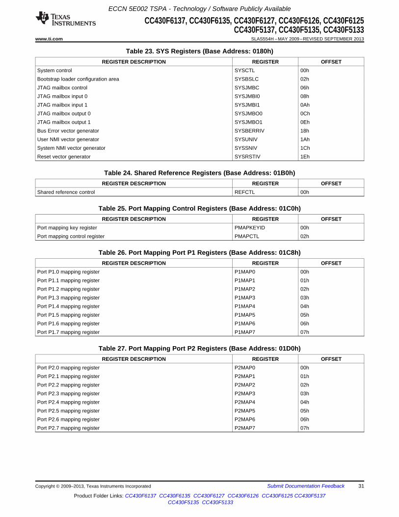
ECCN 5E002 TSPA - Technology / Software Publicly Available
CC430F6137, CC430F6135, CC430F6127, CC430F6126, CC430F6125CC430F5137, CC430F5135, CC430F5133
www.ti.com SLAS554H –MAY 2009–REVISED SEPTEMBER 2013
Table 23. SYS Registers (Base Address: 0180h)REGISTER DESCRIPTION REGISTER OFFSET
System control SYSCTL 00hBootstrap loader configuration area SYSBSLC 02hJTAG mailbox control SYSJMBC 06hJTAG mailbox input 0 SYSJMBI0 08hJTAG mailbox input 1 SYSJMBI1 0AhJTAG mailbox output 0 SYSJMBO0 0ChJTAG mailbox output 1 SYSJMBO1 0EhBus Error vector generator SYSBERRIV 18hUser NMI vector generator SYSUNIV 1AhSystem NMI vector generator SYSSNIV 1ChReset vector generator SYSRSTIV 1Eh
Table 24. Shared Reference Registers (Base Address: 01B0h)REGISTER DESCRIPTION REGISTER OFFSET
Shared reference control REFCTL 00h
Table 25. Port Mapping Control Registers (Base Address: 01C0h)REGISTER DESCRIPTION REGISTER OFFSET
Port mapping key register PMAPKEYID 00hPort mapping control register PMAPCTL 02h
Table 26. Port Mapping Port P1 Registers (Base Address: 01C8h)REGISTER DESCRIPTION REGISTER OFFSET
Port P1.0 mapping register P1MAP0 00hPort P1.1 mapping register P1MAP1 01hPort P1.2 mapping register P1MAP2 02hPort P1.3 mapping register P1MAP3 03hPort P1.4 mapping register P1MAP4 04hPort P1.5 mapping register P1MAP5 05hPort P1.6 mapping register P1MAP6 06hPort P1.7 mapping register P1MAP7 07h
Table 27. Port Mapping Port P2 Registers (Base Address: 01D0h)REGISTER DESCRIPTION REGISTER OFFSET
Port P2.0 mapping register P2MAP0 00hPort P2.1 mapping register P2MAP1 01hPort P2.2 mapping register P2MAP2 02hPort P2.3 mapping register P2MAP3 03hPort P2.4 mapping register P2MAP4 04hPort P2.5 mapping register P2MAP5 05hPort P2.6 mapping register P2MAP6 06hPort P2.7 mapping register P2MAP7 07h
Copyright © 2009–2013, Texas Instruments Incorporated Submit Documentation Feedback 31
Product Folder Links: CC430F6137 CC430F6135 CC430F6127 CC430F6126 CC430F6125 CC430F5137CC430F5135 CC430F5133

ECCN 5E002 TSPA - Technology / Software Publicly Available
CC430F6137, CC430F6135, CC430F6127, CC430F6126, CC430F6125CC430F5137, CC430F5135, CC430F5133SLAS554H –MAY 2009–REVISED SEPTEMBER 2013 www.ti.com
Table 28. Port Mapping Port P3 Registers (Base Address: 01D8h)REGISTER DESCRIPTION REGISTER OFFSET
Port P3.0 mapping register P3MAP0 00hPort P3.1 mapping register P3MAP1 01hPort P3.2 mapping register P3MAP2 02hPort P3.3 mapping register P3MAP3 03hPort P3.4 mapping register P3MAP4 04hPort P3.5 mapping register P3MAP5 05hPort P3.6 mapping register P3MAP6 06hPort P3.7 mapping register P3MAP7 07h
Table 29. Port P1, P2 Registers (Base Address: 0200h)REGISTER DESCRIPTION REGISTER OFFSET
Port P1 input P1IN 00hPort P1 output P1OUT 02hPort P1 direction P1DIR 04hPort P1 pullup/pulldown enable P1REN 06hPort P1 drive strength P1DS 08hPort P1 selection P1SEL 0AhPort P1 interrupt vector word P1IV 0EhPort P1 interrupt edge select P1IES 18hPort P1 interrupt enable P1IE 1AhPort P1 interrupt flag P1IFG 1ChPort P2 input P2IN 01hPort P2 output P2OUT 03hPort P2 direction P2DIR 05hPort P2 pullup/pulldown enable P2REN 07hPort P2 drive strength P2DS 09hPort P2 selection P2SEL 0BhPort P2 interrupt vector word P2IV 1EhPort P2 interrupt edge select P2IES 19hPort P2 interrupt enable P2IE 1BhPort P2 interrupt flag P2IFG 1Dh
Table 30. Port P3, P4 Registers (Base Address: 0220h)REGISTER DESCRIPTION REGISTER OFFSET
Port P3 input P3IN 00hPort P3 output P3OUT 02hPort P3 direction P3DIR 04hPort P3 pullup/pulldown enable P3REN 06hPort P3 drive strength P3DS 08hPort P3 selection P3SEL 0AhPort P4 input P4IN 01hPort P4 output P4OUT 03hPort P4 direction P4DIR 05hPort P4 pullup/pulldown enable P4REN 07hPort P4 drive strength P4DS 09hPort P4 selection P4SEL 0Bh
32 Submit Documentation Feedback Copyright © 2009–2013, Texas Instruments Incorporated
Product Folder Links: CC430F6137 CC430F6135 CC430F6127 CC430F6126 CC430F6125 CC430F5137CC430F5135 CC430F5133

ECCN 5E002 TSPA - Technology / Software Publicly Available
CC430F6137, CC430F6135, CC430F6127, CC430F6126, CC430F6125CC430F5137, CC430F5135, CC430F5133
www.ti.com SLAS554H –MAY 2009–REVISED SEPTEMBER 2013
Table 31. Port P5 Registers (Base Address: 0240h)REGISTER DESCRIPTION REGISTER OFFSET
Port P5 input P5IN 00hPort P5 output P5OUT 02hPort P5 direction P5DIR 04hPort P5 pullup/pulldown enable P5REN 06hPort P5 drive strength P5DS 08hPort P5 selection P5SEL 0Ah
Table 32. Port J Registers (Base Address: 0320h)REGISTER DESCRIPTION REGISTER OFFSET
Port PJ input PJIN 00hPort PJ output PJOUT 02hPort PJ direction PJDIR 04hPort PJ pullup/pulldown enable PJREN 06hPort PJ drive strength PJDS 08h
Table 33. TA0 Registers (Base Address: 0340h)REGISTER DESCRIPTION REGISTER OFFSET
TA0 control TA0CTL 00hCapture/compare control 0 TA0CCTL0 02hCapture/compare control 1 TA0CCTL1 04hCapture/compare control 2 TA0CCTL2 06hCapture/compare control 3 TA0CCTL3 08hCapture/compare control 4 TA0CCTL4 0AhTA0 counter register TA0R 10hCapture/compare register 0 TA0CCR0 12hCapture/compare register 1 TA0CCR1 14hCapture/compare register 2 TA0CCR2 16hCapture/compare register 3 TA0CCR3 18hCapture/compare register 4 TA0CCR4 1AhTA0 expansion register 0 TA0EX0 20hTA0 interrupt vector TA0IV 2Eh
Table 34. TA1 Registers (Base Address: 0380h)REGISTER DESCRIPTION REGISTER OFFSET
TA1 control TA1CTL 00hCapture/compare control 0 TA1CCTL0 02hCapture/compare control 1 TA1CCTL1 04hCapture/compare control 2 TA1CCTL2 06hTA1 counter register TA1R 10hCapture/compare register 0 TA1CCR0 12hCapture/compare register 1 TA1CCR1 14hCapture/compare register 2 TA1CCR2 16hTA1 expansion register 0 TA1EX0 20hTA1 interrupt vector TA1IV 2Eh
Copyright © 2009–2013, Texas Instruments Incorporated Submit Documentation Feedback 33
Product Folder Links: CC430F6137 CC430F6135 CC430F6127 CC430F6126 CC430F6125 CC430F5137CC430F5135 CC430F5133

ECCN 5E002 TSPA - Technology / Software Publicly Available
CC430F6137, CC430F6135, CC430F6127, CC430F6126, CC430F6125CC430F5137, CC430F5135, CC430F5133SLAS554H –MAY 2009–REVISED SEPTEMBER 2013 www.ti.com
Table 35. Real Time Clock Registers (Base Address: 04A0h)REGISTER DESCRIPTION REGISTER OFFSET
RTC control 0 RTCCTL0 00hRTC control 1 RTCCTL1 01hRTC control 2 RTCCTL2 02hRTC control 3 RTCCTL3 03hRTC prescaler 0 control RTCPS0CTL 08hRTC prescaler 1 control RTCPS1CTL 0AhRTC prescaler 0 RTCPS0 0ChRTC prescaler 1 RTCPS1 0DhRTC interrupt vector word RTCIV 0EhRTC seconds/counter register 1 RTCSEC/RTCNT1 10hRTC minutes/counter register 2 RTCMIN/RTCNT2 11hRTC hours/counter register 3 RTCHOUR/RTCNT3 12hRTC day of week/counter register 4 RTCDOW/RTCNT4 13hRTC days RTCDAY 14hRTC month RTCMON 15hRTC year low RTCYEARL 16hRTC year high RTCYEARH 17hRTC alarm minutes RTCAMIN 18hRTC alarm hours RTCAHOUR 19hRTC alarm day of week RTCADOW 1AhRTC alarm days RTCADAY 1Bh
Table 36. 32-Bit Hardware Multiplier Registers (Base Address: 04C0h)REGISTER DESCRIPTION REGISTER OFFSET
16-bit operand 1 – multiply MPY 00h16-bit operand 1 – signed multiply MPYS 02h16-bit operand 1 – multiply accumulate MAC 04h16-bit operand 1 – signed multiply accumulate MACS 06h16-bit operand 2 OP2 08h16 × 16 result low word RESLO 0Ah16 × 16 result high word RESHI 0Ch16 × 16 sum extension register SUMEXT 0Eh32-bit operand 1 – multiply low word MPY32L 10h32-bit operand 1 – multiply high word MPY32H 12h32-bit operand 1 – signed multiply low word MPYS32L 14h32-bit operand 1 – signed multiply high word MPYS32H 16h32-bit operand 1 – multiply accumulate low word MAC32L 18h32-bit operand 1 – multiply accumulate high word MAC32H 1Ah32-bit operand 1 – signed multiply accumulate low word MACS32L 1Ch32-bit operand 1 – signed multiply accumulate high word MACS32H 1Eh32-bit operand 2 – low word OP2L 20h32-bit operand 2 – high word OP2H 22h32 × 32 result 0 – least significant word RES0 24h32 × 32 result 1 RES1 26h32 × 32 result 2 RES2 28h32 × 32 result 3 – most significant word RES3 2AhMPY32 control register 0 MPY32CTL0 2Ch
34 Submit Documentation Feedback Copyright © 2009–2013, Texas Instruments Incorporated
Product Folder Links: CC430F6137 CC430F6135 CC430F6127 CC430F6126 CC430F6125 CC430F5137CC430F5135 CC430F5133

ECCN 5E002 TSPA - Technology / Software Publicly Available
CC430F6137, CC430F6135, CC430F6127, CC430F6126, CC430F6125CC430F5137, CC430F5135, CC430F5133
www.ti.com SLAS554H –MAY 2009–REVISED SEPTEMBER 2013
Table 37. DMA Module Control Registers (Base Address: 0500h)REGISTER DESCRIPTION REGISTER OFFSET
DMA module control 0 DMACTL0 00hDMA module control 1 DMACTL1 02hDMA module control 2 DMACTL2 04hDMA module control 3 DMACTL3 06hDMA module control 4 DMACTL4 08hDMA interrupt vector DMAIV 0Ah
Table 38. DMA Channel 0 Registers (Base Address: 0510h)REGISTER DESCRIPTION REGISTER OFFSET
DMA channel 0 control DMA0CTL 00hDMA channel 0 source address low DMA0SAL 02hDMA channel 0 source address high DMA0SAH 04hDMA channel 0 destination address low DMA0DAL 06hDMA channel 0 destination address high DMA0DAH 08hDMA channel 0 transfer size DMA0SZ 0Ah
Table 39. DMA Channel 1 Registers (Base Address: 0520h)REGISTER DESCRIPTION REGISTER OFFSET
DMA channel 1 control DMA1CTL 00hDMA channel 1 source address low DMA1SAL 02hDMA channel 1 source address high DMA1SAH 04hDMA channel 1 destination address low DMA1DAL 06hDMA channel 1 destination address high DMA1DAH 08hDMA channel 1 transfer size DMA1SZ 0Ah
Table 40. DMA Channel 2 Registers (Base Address: 0530h)REGISTER DESCRIPTION REGISTER OFFSET
DMA channel 2 control DMA2CTL 00hDMA channel 2 source address low DMA2SAL 02hDMA channel 2 source address high DMA2SAH 04hDMA channel 2 destination address low DMA2DAL 06hDMA channel 2 destination address high DMA2DAH 08hDMA channel 2 transfer size DMA2SZ 0Ah
Copyright © 2009–2013, Texas Instruments Incorporated Submit Documentation Feedback 35
Product Folder Links: CC430F6137 CC430F6135 CC430F6127 CC430F6126 CC430F6125 CC430F5137CC430F5135 CC430F5133

ECCN 5E002 TSPA - Technology / Software Publicly Available
CC430F6137, CC430F6135, CC430F6127, CC430F6126, CC430F6125CC430F5137, CC430F5135, CC430F5133SLAS554H –MAY 2009–REVISED SEPTEMBER 2013 www.ti.com
Table 41. USCI_A0 Registers (Base Address: 05C0h)REGISTER DESCRIPTION REGISTER OFFSET
USCI control 1 UCA0CTL1 00hUSCI control 0 UCA0CTL0 01hUSCI baud rate 0 UCA0BR0 06hUSCI baud rate 1 UCA0BR1 07hUSCI modulation control UCA0MCTL 08hUSCI status UCA0STAT 0AhUSCI receive buffer UCA0RXBUF 0ChUSCI transmit buffer UCA0TXBUF 0EhUSCI LIN control UCA0ABCTL 10hUSCI IrDA transmit control UCA0IRTCTL 12hUSCI IrDA receive control UCA0IRRCTL 13hUSCI interrupt enable UCA0IE 1ChUSCI interrupt flags UCA0IFG 1DhUSCI interrupt vector word UCA0IV 1Eh
Table 42. USCI_B0 Registers (Base Address: 05E0h)REGISTER DESCRIPTION REGISTER OFFSET
USCI synchronous control 1 UCB0CTL1 00hUSCI synchronous control 0 UCB0CTL0 01hUSCI synchronous bit rate 0 UCB0BR0 06hUSCI synchronous bit rate 1 UCB0BR1 07hUSCI synchronous status UCB0STAT 0AhUSCI synchronous receive buffer UCB0RXBUF 0ChUSCI synchronous transmit buffer UCB0TXBUF 0EhUSCI I2C own address UCB0I2COA 10hUSCI I2C slave address UCB0I2CSA 12hUSCI interrupt enable UCB0IE 1ChUSCI interrupt flags UCB0IFG 1DhUSCI interrupt vector word UCB0IV 1Eh
36 Submit Documentation Feedback Copyright © 2009–2013, Texas Instruments Incorporated
Product Folder Links: CC430F6137 CC430F6135 CC430F6127 CC430F6126 CC430F6125 CC430F5137CC430F5135 CC430F5133

ECCN 5E002 TSPA - Technology / Software Publicly Available
CC430F6137, CC430F6135, CC430F6127, CC430F6126, CC430F6125CC430F5137, CC430F5135, CC430F5133
www.ti.com SLAS554H –MAY 2009–REVISED SEPTEMBER 2013
Table 43. ADC12_A Registers (Base Address: 0700h)REGISTER DESCRIPTION REGISTER OFFSET
Control register 0 ADC12CTL0 00hControl register 1 ADC12CTL1 02hControl register 2 ADC12CTL2 04hInterrupt-flag register ADC12IFG 0AhInterrupt-enable register ADC12IE 0ChInterrupt-vector-word register ADC12IV 0EhADC memory-control register 0 ADC12MCTL0 10hADC memory-control register 1 ADC12MCTL1 11hADC memory-control register 2 ADC12MCTL2 12hADC memory-control register 3 ADC12MCTL3 13hADC memory-control register 4 ADC12MCTL4 14hADC memory-control register 5 ADC12MCTL5 15hADC memory-control register 6 ADC12MCTL6 16hADC memory-control register 7 ADC12MCTL7 17hADC memory-control register 8 ADC12MCTL8 18hADC memory-control register 9 ADC12MCTL9 19hADC memory-control register 10 ADC12MCTL10 1AhADC memory-control register 11 ADC12MCTL11 1BhADC memory-control register 12 ADC12MCTL12 1ChADC memory-control register 13 ADC12MCTL13 1DhADC memory-control register 14 ADC12MCTL14 1EhADC memory-control register 15 ADC12MCTL15 1FhConversion memory 0 ADC12MEM0 20hConversion memory 1 ADC12MEM1 22hConversion memory 2 ADC12MEM2 24hConversion memory 3 ADC12MEM3 26hConversion memory 4 ADC12MEM4 28hConversion memory 5 ADC12MEM5 2AhConversion memory 6 ADC12MEM6 2ChConversion memory 7 ADC12MEM7 2EhConversion memory 8 ADC12MEM8 30hConversion memory 9 ADC12MEM9 32hConversion memory 10 ADC12MEM10 34hConversion memory 11 ADC12MEM11 36hConversion memory 12 ADC12MEM12 38hConversion memory 13 ADC12MEM13 3AhConversion memory 14 ADC12MEM14 3ChConversion memory 15 ADC12MEM15 3Eh
Copyright © 2009–2013, Texas Instruments Incorporated Submit Documentation Feedback 37
Product Folder Links: CC430F6137 CC430F6135 CC430F6127 CC430F6126 CC430F6125 CC430F5137CC430F5135 CC430F5133

ECCN 5E002 TSPA - Technology / Software Publicly Available
CC430F6137, CC430F6135, CC430F6127, CC430F6126, CC430F6125CC430F5137, CC430F5135, CC430F5133SLAS554H –MAY 2009–REVISED SEPTEMBER 2013 www.ti.com
Table 44. Comparator_B Registers (Base Address: 08C0h)REGISTER DESCRIPTION REGISTER OFFSET
Comp_B control register 0 CBCTL0 00hComp_B control register 1 CBCTL1 02hComp_B control register 2 CBCTL2 04hComp_B control register 3 CBCTL3 06hComp_B interrupt register CBINT 0ChComp_B interrupt vector word CBIV 0Eh
Table 45. AES Accelerator Registers (Base Address: 09C0h)REGISTER DESCRIPTION REGISTER OFFSET
AES accelerator control register 0 AESACTL0 00hReserved 02hAES accelerator status register AESASTAT 04hAES accelerator key register AESAKEY 06hAES accelerator data in register AESADIN 008hAES accelerator data out register AESADOUT 00Ah
Table 46. LCD_B Registers (Base Address: 0A00h)REGISTER DESCRIPTION REGISTER OFFSET
LCD_B control register 0 LCDBCTL0 000hLCD_B control register 1 LCDBCTL1 002hLCD_B blinking control register LCDBBLKCTL 004hLCD_B memory control register LCDBMEMCTL 006hLCD_B voltage control register LCDBVCTL 008hLCD_B port control register 0 LCDBPCTL0 00AhLCD_B port control register 1 LCDBPCTL1 00ChLCD_B charge pump control register LCDBCTL0 012hLCD_B interrupt vector word LCDBIV 01EhLCD_B memory 1 LCDM1 020hLCD_B memory 2 LCDM2 021h...LCD_B memory 14 LCDM14 02DhLCD_B blinking memory 1 LCDBM1 040hLCD_B blinking memory 2 LCDBM2 041h...LCD_B blinking memory 14 LCDBM14 04Dh
38 Submit Documentation Feedback Copyright © 2009–2013, Texas Instruments Incorporated
Product Folder Links: CC430F6137 CC430F6135 CC430F6127 CC430F6126 CC430F6125 CC430F5137CC430F5135 CC430F5133

ECCN 5E002 TSPA - Technology / Software Publicly Available
CC430F6137, CC430F6135, CC430F6127, CC430F6126, CC430F6125CC430F5137, CC430F5135, CC430F5133
www.ti.com SLAS554H –MAY 2009–REVISED SEPTEMBER 2013
Table 47. Radio Interface Registers (Base Address: 0F00h)REGISTER DESCRIPTION REGISTER OFFSET
Radio interface control register 0 RF1AIFCTL0 00hRadio interface control register 1 RF1AIFCTL1 02hRadio interface error flag register RF1AIFERR 06hRadio interface error vector word RF1AIFERRV 0ChRadio interface interrupt vector word RF1AIFIV 0EhRadio instruction word register RF1AINSTRW 10hRadio instruction word register, 1-byte auto-read RF1AINSTR1W 12hRadio instruction word register, 2-byte auto-read RF1AINSTR2W 14hRadio data in register RF1ADINW 16hRadio status word register RF1ASTATW 20hRadio status word register, 1-byte auto-read RF1ASTAT1W 22hRadio status word register, 2-byte auto-read RF1AISTAT2W 24hRadio data out register RF1ADOUTW 28hRadio data out register, 1-byte auto-read RF1ADOUT1W 2AhRadio data out register, 2-byte auto-read RF1ADOUT2W 2ChRadio core signal input register RF1AIN 30hRadio core interrupt flag register RF1AIFG 32hRadio core interrupt edge select register RF1AIES 34hRadio core interrupt enable register RF1AIE 36hRadio core interrupt vector word RF1AIV 38h
Copyright © 2009–2013, Texas Instruments Incorporated Submit Documentation Feedback 39
Product Folder Links: CC430F6137 CC430F6135 CC430F6127 CC430F6126 CC430F6125 CC430F5137CC430F5135 CC430F5133

ECCN 5E002 TSPA - Technology / Software Publicly Available
CC430F6137, CC430F6135, CC430F6127, CC430F6126, CC430F6125CC430F5137, CC430F5135, CC430F5133SLAS554H –MAY 2009–REVISED SEPTEMBER 2013 www.ti.com
Absolute Maximum Ratings (1)
over operating free-air temperature range (unless otherwise noted)Voltage applied at DVCC and AVCC pins to VSS –0.3 V to 4.1 V
–0.3 V to (VCC + 0.3 V),Voltage applied to any pin (excluding VCORE, RF_P, RF_N, and R_BIAS) (2)4.1 V Max
Voltage applied to VCORE, RF_P, RF_N, and R_BIAS (2) –0.3 V to 2.0 VInput RF level at pins RF_P and RF_N 10 dBmDiode current at any device terminal ±2 mAStorage temperature range (3), Tstg –55°C to 150°CMaximum junction temperature, TJ 95°C
(1) Stresses beyond those listed under Absolute Maximum Ratings may cause permanent damage to the device. These are stress ratingsonly, and functional operation of the device at these or any other conditions beyond those indicated under Recommended OperatingConditions is not implied. Exposure to absolute-maximum-rated conditions for extended periods may affect device reliability.
(2) All voltages referenced to VSS.(3) Higher temperature may be applied during board soldering according to the current JEDEC J-STD-020 specification with peak reflow
temperatures not higher than classified on the device label on the shipping boxes or reels.
Thermal Packaging Characteristics CC430F51xxLow-K board 48 QFN (RGZ) 98°C/W
θJA Junction-to-ambient thermal resistance, still airHigh-K board 48 QFN (RGZ) 28°C/W
Thermal Packaging Characteristics CC430F61xxLow-K board 64 QFN (RGC) 83°C/W
θJA Junction-to-ambient thermal resistance, still airHigh-K board 64 QFN (RGC) 26°C/W
Recommended Operating ConditionsTypical values are specified at VCC = 3.3 V and TA = 25°C (unless otherwise noted)
MIN NOM MAX UNITSupply voltage range applied at all DVCC and AVCC PMMCOREVx = 0 1.8 3.6pins (1) during program execution and flash programming (default after POR)VCC Vwith PMM default settings, Radio is not operational with
PMMCOREVx = 1 2.0 3.6PMMCOREVx = 0 or 1 (2) (3)
Supply voltage range applied at all DVCC and AVCC PMMCOREVx = 2 2.2 3.6VCC pins (1) during program execution, flash programming, and V
PMMCOREVx = 3 2.4 3.6radio operation with PMM default settings (2) (3)
Supply voltage range applied at all DVCC and AVCCpins (1) during program execution, flash programming and PMMCOREVx = 2,
VCC radio operation with PMMCOREVx = 2, high-side SVS SVSHRVLx = SVSHRRRLx = 1 2.0 3.6 Vlevel lowered (SVSHRVL = SVSMHRRL = 1) or high-side or SVSHE = 0SVS disabled (SVSHE = 0) (2) (3) (4)
Supply voltage applied at the exposed die attach VSS andVSS 0 VAVSS pinTA Operating free-air temperature –40 85 °CTJ Operating junction temperature –40 85 °CCVCORE Recommended capacitor at VCORE (5) 470 nFCDVCC/ Capacitor ratio of capacitor at DVCC to capacitor at 10CVCORE VCORE
(1) It is recommended to power AVCC and DVCC from the same source. A maximum difference of 0.3 V between AVCC and DVCC can betolerated during power up and operation.
(2) Modules may have a different supply voltage range specification. See the specification of the respective module in this data sheet.(3) The minimum supply voltage is defined by the supervisor SVS levels when it is enabled. See the PMM, SVS High Side threshold
parameters for the exact values and further details.(4) Lowering the high-side SVS level or disabling the high-side SVS might cause the LDO to operate out of regulation, but the core voltage
will still stay within its limits and is still supervised by the low-side SVS ensuring reliable operation.(5) A capacitor tolerance of ±20% or better is required.
40 Submit Documentation Feedback Copyright © 2009–2013, Texas Instruments Incorporated
Product Folder Links: CC430F6137 CC430F6135 CC430F6127 CC430F6126 CC430F6125 CC430F5137CC430F5135 CC430F5133

2.01.8
8
0
12
20
Syste
m F
requency -
MH
z
Supply Voltage - V
The numbers within the fields denote the supported PMMCOREVx settings.
2.2 2.4 3.6
0, 1, 2, 30, 1, 20, 10
1, 2, 31, 21
2, 3
3
2
16
ECCN 5E002 TSPA - Technology / Software Publicly Available
CC430F6137, CC430F6135, CC430F6127, CC430F6126, CC430F6125CC430F5137, CC430F5135, CC430F5133
www.ti.com SLAS554H –MAY 2009–REVISED SEPTEMBER 2013
Recommended Operating Conditions (continued)Typical values are specified at VCC = 3.3 V and TA = 25°C (unless otherwise noted)
MIN NOM MAX UNITPMMCOREVx = 0 0 8(default condition)PMMCOREVx = 1 0 12fSYSTEM Processor (MCLK) frequency (6) (see Figure 2) MHzPMMCOREVx = 2 0 16PMMCOREVx = 3 0 20
PINT Internal power dissipation VCC × I(DVCC) W(VCC - VIOH) × IIOH +PIO I/O power dissipation of I/O pins powered by DVCC WVIOL × IIOL
PMAX Maximum allowed power dissipation, PMAX > PIO + PINT (TJ - TA) / θJA W
(6) Modules may have a different maximum input clock specification. See the specification of the respective module in this data sheet.
Figure 2. Maximum System Frequency
Copyright © 2009–2013, Texas Instruments Incorporated Submit Documentation Feedback 41
Product Folder Links: CC430F6137 CC430F6135 CC430F6127 CC430F6126 CC430F6125 CC430F5137CC430F5135 CC430F5133

0
1
2
3
4
5
0 5 10 15 20
MCLK Frequency - MHz
I AM
-A
cti
ve
Mo
de
Su
pp
lyC
urr
en
t-
mA
VCC = 3.0 V
PMMVCOREx=2
PMMVCOREx=0
PMMVCOREx=1
PMMVCOREx=3
ECCN 5E002 TSPA - Technology / Software Publicly Available
CC430F6137, CC430F6135, CC430F6127, CC430F6126, CC430F6125CC430F5137, CC430F5135, CC430F5133SLAS554H –MAY 2009–REVISED SEPTEMBER 2013 www.ti.com
Electrical Characteristics
Active Mode Supply Current Into VCC Excluding External Currentover recommended operating free-air temperature (unless otherwise noted) (1) (2) (3)
FREQUENCY (fDCO = fMCLK = fSMCLK)EXECUTIONPARAMETER VCC PMMCOREVx 1 MHz 8 MHz 12 MHz 16 MHz 20 MHz UNITMEMORY
TYP MAX TYP MAX TYP MAX TYP MAX TYP MAX0 0.23 0.26 1.35 1.601 0.25 0.28 1.55 2.30 2.65
IAM, Flash(4) Flash 3.0 V mA
2 0.27 0.30 1.75 2.60 3.45 3.903 0.28 0.32 1.85 2.75 3.65 4.55 5.100 0.18 0.20 0.95 1.101 0.20 0.22 1.10 1.60 1.85
IAM, RAM(5) RAM 3.0 V mA
2 0.21 0.24 1.20 1.80 2.40 2.703 0.22 0.25 1.30 1.90 2.50 3.10 3.60
(1) All inputs are tied to 0 V or to VCC. Outputs do not source or sink any current.(2) The currents are characterized with a Micro Crystal MS1V-T1K crystal with a load capacitance of 12.5 pF. The internal and external load
capacitance are chosen to closely match the required 12.5 pF.(3) Characterized with program executing typical data processing.
fACLK = 32786 Hz, fDCO = fMCLK = fSMCLK at specified frequency.XTS = CPUOFF = SCG0 = SCG1 = OSCOFF= SMCLKOFF = 0.
(4) Active mode supply current when program executes in flash at a nominal supply voltage of 3.0 V.(5) Active mode supply current when program executes in RAM at a nominal supply voltage of 3.0 V.
Typical Characteristics - Active Mode Supply Currents
Active Mode Supply Currentvs
MCLK Frequency
Figure 3.
42 Submit Documentation Feedback Copyright © 2009–2013, Texas Instruments Incorporated
Product Folder Links: CC430F6137 CC430F6135 CC430F6127 CC430F6126 CC430F6125 CC430F5137CC430F5135 CC430F5133

ECCN 5E002 TSPA - Technology / Software Publicly Available
CC430F6137, CC430F6135, CC430F6127, CC430F6126, CC430F6125CC430F5137, CC430F5135, CC430F5133
www.ti.com SLAS554H –MAY 2009–REVISED SEPTEMBER 2013
Low-Power Mode Supply Currents (Into VCC) Excluding External Currentover recommended ranges of supply voltage and operating free-air temperature (unless otherwise noted) (1) (2)
Temperature (TA)
PARAMETER VCC PMMCOREVx -40°C 25°C 60°C 85°C UNIT
TYP MAX TYP MAX TYP MAX TYP MAX
2.2 V 0 80 100 80 100 80 100 80 100ILPM0,1MHz Low-power mode 0 (3) (4) µA
3.0 V 3 90 110 90 110 90 110 90 110
2.2 V 0 6.5 11 6.5 11 6.5 11 6.5 11ILPM2 Low-power mode 2 (5) (4) µA
3.0 V 3 7.5 12 7.5 12 7.5 12 7.5 12
0 1.8 2.0 2.6 3.0 4.0 4.4 5.9
1 1.9 2.1 3.2 4.8Low-power mode 3, crystalILPM3,XT1LF 3.0 V µAmode (6) (4)2 2.0 2.2 3.4 5.1
3 2.0 2.2 2.9 3.5 4.8 5.3 7.4
0 0.9 1.1 2.3 2.1 3.7 3.5 5.6
1 1.0 1.2 2.3 3.9Low-power mode 3,ILPM3,VLO 3.0 V µAVLO mode (7) (4)2 1.1 1.3 2.5 4.2
3 1.1 1.3 2.6 2.6 4.5 4.4 7.1
0 0.8 1.0 2.2 2.0 3.6 3.4 5.5
1 0.9 1.1 2.2 3.8ILPM4 Low-power mode 4 (8) (4) 3.0 V µA
2 1.0 1.2 2.4 4.1
3 1.0 1.2 2.5 2.5 4.4 4.3 7.0
(1) All inputs are tied to 0 V or to VCC. Outputs do not source or sink any current.(2) The currents are characterized with a Micro Crystal MS1V-T1K crystal with a load capacitance of 12.5 pF. The internal and external load
capacitance are chosen to closely match the required 12.5 pF.(3) Current for watchdog timer clocked by SMCLK included. ACLK = low frequency crystal operation (XTS = 0, XT1DRIVEx = 0).
CPUOFF = 1, SCG0 = 0, SCG1 = 0, OSCOFF = 0 (LPM0); fACLK = 32768 Hz, fMCLK = 0 MHz, fSMCLK = fDCO = 1 MHz(4) Current for brownout, high side supervisor (SVSH) normal mode included. Low side supervisor and monitors disabled (SVSL, SVML).
High side monitor disabled (SVMH). RAM retention enabled.(5) Current for watchdog timer and RTC clocked by ACLK included. ACLK = low frequency crystal operation (XTS = 0, XT1DRIVEx = 0).
CPUOFF = 1, SCG0 = 0, SCG1 = 1, OSCOFF = 0 (LPM2); fACLK = 32768 Hz, fMCLK = 0 MHz, fSMCLK = fDCO = 0 MHz; DCO setting = 1MHz operation, DCO bias generator enabled.
(6) Current for watchdog timer and RTC clocked by ACLK included. ACLK = low frequency crystal operation (XTS = 0, XT1DRIVEx = 0).CPUOFF = 1, SCG0 = 1, SCG1 = 1, OSCOFF = 0 (LPM3); fACLK = 32768 Hz, fMCLK = fSMCLK = fDCO = 0 MHz
(7) Current for watchdog timer and RTC clocked by ACLK included. ACLK = VLO.CPUOFF = 1, SCG0 = 1, SCG1 = 1, OSCOFF = 0 (LPM3); fACLK = fVLO, fMCLK = fSMCLK = fDCO = 0 MHz
(8) CPUOFF = 1, SCG0 = 1, SCG1 = 1, OSCOFF = 1 (LPM4); fDCO = fACLK = fMCLK = fSMCLK = 0 MHz
Copyright © 2009–2013, Texas Instruments Incorporated Submit Documentation Feedback 43
Product Folder Links: CC430F6137 CC430F6135 CC430F6127 CC430F6126 CC430F6125 CC430F5137CC430F5135 CC430F5133

0
1
2
3
4
5
-40 -20 0 20 40 60 80
TA - Free-Air Temperature - °C
I LP
M3
,XT
1L
F-
LP
M3
Su
pp
lyC
urr
en
t-
uA
VCC = 3.0 V
PMMCOREVx = 3
PMMCOREVx = 0
0
1
2
3
4
5
-40 -20 0 20 40 60 80
TA - Free-Air Temperature - °C
I LP
M4-
LP
M4
Su
pp
lyC
urr
en
t-
uA
VDD = 3.0 V
PMMCOREVx = 3
PMMCOREVx = 0
ECCN 5E002 TSPA - Technology / Software Publicly Available
CC430F6137, CC430F6135, CC430F6127, CC430F6126, CC430F6125CC430F5137, CC430F5135, CC430F5133SLAS554H –MAY 2009–REVISED SEPTEMBER 2013 www.ti.com
Typical Characteristics - Low-Power Mode Supply Currents
LPM3 Supply Current LPM4 Supply Currentvs vs
Temperature Temperature
Figure 4. Figure 5.
44 Submit Documentation Feedback Copyright © 2009–2013, Texas Instruments Incorporated
Product Folder Links: CC430F6137 CC430F6135 CC430F6127 CC430F6126 CC430F6125 CC430F5137CC430F5135 CC430F5133

ECCN 5E002 TSPA - Technology / Software Publicly Available
CC430F6137, CC430F6135, CC430F6127, CC430F6126, CC430F6125CC430F5137, CC430F5135, CC430F5133
www.ti.com SLAS554H –MAY 2009–REVISED SEPTEMBER 2013
Low-Power Mode with LCD Supply Currents (Into VCC) Excluding External Currentover recommended ranges of supply voltage and operating free-air temperature (unless otherwise noted) (1) (2)
Temperature (TA)PARAMETER VCC PMMCOREVx -40°C 25°C 60°C 85°C UNIT
TYP MAX TYP MAX TYP MAX TYP MAX0 2.2 2.4 3.5 4.9
Low-power mode 3ILPM3 1 2.3 2.5 3.7 5.3(LPM3) current, LCD 4-LCD, 3.0 V µAmux mode, external 2 2.4 2.6 3.9 5.6ext. bias biasing (3) (4)3 2.4 2.6 4.0 5.80 3.1 3.3 4.0 4.3 5.8 7.4Low-power mode 3
ILPM3 (LPM3) current, LCD 4- 1 3.2 3.4 4.5 6.2LCD, mux mode, internal 3.0 V µA
2 3.3 3.5 4.7 6.5int. bias biasing, charge pumpdisabled (3) (5) 3 3.3 3.5 4.3 4.8 6.7 8.9
0 4.02.2 V 1 4.1
Low-power mode 3 2 4.2(LPM3) current, LCD 4-ILPM3 mux mode, internal 0 4.2 µALCD,CP biasing, charge pump 1 4.3enabled (3) (6) 3.0 V2 4.53 4.5
(1) All inputs are tied to 0 V or to VCC. Outputs do not source or sink any current.(2) The currents are characterized with a Micro Crystal MS1V-T1K crystal with a load capacitance of 12.5 pF. The internal and external load
capacitance are chosen to closely match the required 12.5 pF.(3) Current for watchdog timer and RTC clocked by ACLK included. ACLK = low frequency crystal operation (XTS = 0, XT1DRIVEx = 0).
CPUOFF = 1, SCG0 = 1, SCG1 = 1, OSCOFF = 0 (LPM3); fACLK = 32768 Hz, fMCLK = fSMCLK = fDCO = 0 MHzCurrent for brownout, high side supervisor (SVSH) normal mode included. Low side supervisor and monitors disabled (SVSL, SVML).High side monitor disabled (SVMH). RAM retention enabled.
(4) LCDMx = 11 (4-mux mode), LCDREXT = 1, LCDEXTBIAS = 1 (external biasing), LCD2B = 0 (1/3 bias), LCDCPEN = 0 (charge pumpdisabled), LCDSSEL=0, LCDPREx=101, LCDDIVx=00011 (fLCD = 32768 Hz/32/4 = 256 Hz)Current through external resistors not included (voltage levels are supplied by test equipment).Even segments S0, S2,...=0, odd segments S1, S3,...=1. No LCD panel load.
(5) LCDMx = 11 (4-mux mode), LCDREXT = 0, LCDEXTBIAS = 0 (internal biasing), LCD2B = 0 (1/3 bias), LCDCPEN = 0 (charge pumpdisabled), LCDSSEL=0, LCDPREx=101, LCDDIVx=00011 (fLCD = 32768 Hz/32/4 = 256 Hz)Even segments S0, S2,...=0, odd segments S1, S3,...=1. No LCD panel load.
(6) LCDMx = 11 (4-mux mode), LCDREXT = 0, LCDEXTBIAS = 0 (internal biasing), LCD2B = 0 (1/3 bias), LCDCPEN = 1 (charge pumpenabled), VLCDx = 1000 (VLCD= 3 V typ.), LCDSSEL=0, LCDPREx=101, LCDDIVx=00011 (fLCD = 32768 Hz/32/4 = 256 Hz)Even segments S0, S2,...=0, odd segments S1, S3,...=1. No LCD panel load.
Copyright © 2009–2013, Texas Instruments Incorporated Submit Documentation Feedback 45
Product Folder Links: CC430F6137 CC430F6135 CC430F6127 CC430F6126 CC430F6125 CC430F5137CC430F5135 CC430F5133

ECCN 5E002 TSPA - Technology / Software Publicly Available
CC430F6137, CC430F6135, CC430F6127, CC430F6126, CC430F6125CC430F5137, CC430F5135, CC430F5133SLAS554H –MAY 2009–REVISED SEPTEMBER 2013 www.ti.com
Digital Inputsover recommended ranges of supply voltage and operating free-air temperature (unless otherwise noted)
PARAMETER TEST CONDITIONS VCC MIN TYP MAX UNIT1.8 V 0.80 1.40
VIT+ Positive-going input threshold voltage V3 V 1.50 2.10
1.8 V 0.45 1.00VIT– Negative-going input threshold voltage V
3 V 0.75 1.651.8 V 0.3 0.8
Vhys Input voltage hysteresis (VIT+ – VIT–) V3 V 0.4 1.0
For pullup: VIN = VSSRPull Pullup or pulldown resistor 20 35 50 kΩFor pulldown: VIN = VCC
CI Input capacitance VIN = VSS or VCC 5 pFIlkg(Px.y) High-impedance leakage current (1) (2) 1.8 V, 3 V ±50 nA
Ports with interrupt capabilityExternal interrupt timing (External trigger pulse (see block diagram andt(int) 1.8 V, 3 V 20 nsduration to set interrupt flag) (3) terminal function
descriptions).
(1) The leakage current is measured with VSS or VCC applied to the corresponding pins, unless otherwise noted.(2) The leakage of the digital port pins is measured individually. The port pin is selected for input and the pullup or pulldown resistor is
disabled.(3) An external signal sets the interrupt flag every time the minimum interrupt pulse duration t(int) is met. It may be set by trigger signals
shorter than t(int).
46 Submit Documentation Feedback Copyright © 2009–2013, Texas Instruments Incorporated
Product Folder Links: CC430F6137 CC430F6135 CC430F6127 CC430F6126 CC430F6125 CC430F5137CC430F5135 CC430F5133

ECCN 5E002 TSPA - Technology / Software Publicly Available
CC430F6137, CC430F6135, CC430F6127, CC430F6126, CC430F6125CC430F5137, CC430F5135, CC430F5133
www.ti.com SLAS554H –MAY 2009–REVISED SEPTEMBER 2013
Digital Outputsover recommended ranges of supply voltage and operating free-air temperature (unless otherwise noted)
PARAMETER TEST CONDITIONS VCC MIN MAX UNITI(OHmax) = –1 mA, PxDS.y = 0 (2) VCC – 0.25 VCC1.8 VI(OHmax) = –3 mA, PxDS.y = 0 (3) VCC – 0.60 VCCHigh-level output voltage,VOH VReduced Drive Strength (1) I(OHmax) = –2 mA, PxDS.y = 0 (2) VCC – 0.25 VCC3.0 VI(OHmax) = –6 mA, PxDS.y = 0 (3) VCC – 0.60 VCC
I(OLmax) = 1 mA, PxDS.y = 0 (2) VSS VSS + 0.251.8 V
I(OLmax) = 3 mA, PxDS.y = 0 (3) VSS VSS + 0.60Low-level output voltage,VOL VReduced Drive Strength (1) I(OLmax) = 2 mA, PxDS.y = 0 (2) VSS VSS + 0.253.0 V
I(OLmax) = 6 mA, PxDS.y = 0 (3) VSS VSS + 0.60I(OHmax) = –3 mA, PxDS.y = 1 (2) VCC – 0.25 VCC1.8 VI(OHmax) = –10 mA, PxDS.y = 1 (3) VCC – 0.60 VCCHigh-level output voltage,VOH VFull Drive Strength I(OHmax) = –5 mA, PxDS.y = 1 (2) VCC – 0.25 VCC3 VI(OHmax) = –15 mA, PxDS.y = 1 (3) VCC – 0.60 VCC
I(OLmax) = 3 mA, PxDS.y = 1 (2) VSS VSS + 0.251.8 V
I(OLmax) = 10 mA, PxDS.y = 1 (3) VSS VSS + 0.60Low-level output voltage,VOL VFull Drive Strength I(OLmax) = 5 mA, PxDS.y = 1 (2) VSS VSS + 0.253 V
I(OLmax) = 15 mA, PxDS.y = 1 (3) VSS VSS + 0.60VCC = 1.8 V, 16PMMCOREVx = 0Port output frequencyfPx.y CL = 20 pF, RL
(4) (5) MHz(with load) VCC = 3 V, 25PMMCOREVx = 2VCC = 1.8 V, 16PMMCOREVx = 0
fPort_CLK Clock output frequency CL = 20 pF (5) MHzVCC = 3 V, 25PMMCOREVx = 2
(1) Selecting reduced drive strength may reduce EMI.(2) The maximum total current, I(OHmax) and I(OLmax), for all outputs combined should not exceed ±48 mA to hold the maximum voltage drop
specified.(3) The maximum total current, I(OHmax) and I(OLmax), for all outputs combined should not exceed ±100 mA to hold the maximum voltage
drop specified.(4) A resistive divider with 2 × R1 between VCC and VSS is used as load. The output is connected to the center tap of the divider. For full
drive strength, R1 = 550 Ω. For reduced drive strength, R1 = 1.6 kΩ. CL = 20 pF is connected to the output to VSS.(5) The output voltage reaches at least 10% and 90% VCC at the specified toggle frequency.
Copyright © 2009–2013, Texas Instruments Incorporated Submit Documentation Feedback 47
Product Folder Links: CC430F6137 CC430F6135 CC430F6127 CC430F6126 CC430F6125 CC430F5137CC430F5135 CC430F5133

-25
-20
-15
-10
-5
0
0 0.5 1 1.5 2 2.5 3 3.5
VOH - High-Level Output Voltage - V
I OH
-T
yp
icalH
igh
-LevelO
utp
ut
Cu
rren
t-
mA
VCC = 3.0 VVCC = 3.0 V
P4.3
TA = 25°C
TA = 85°C
-8
-7
-6
-5
-4
-3
-2
-1
0
0 0.5 1 1.5 2
VOH - High-Level Output Voltage - V
I OH
-T
yp
icalH
igh
-LevelO
utp
ut
Cu
rren
t-
mA
VDD = 5.5 VVDD = 5.5 V
VCC = 1.8 V
P4.3
TA = 25°C
TA = 85°C
0
5
10
15
20
25
0 0.5 1 1.5 2 2.5 3 3.5
VOL - Low-Level Output Voltage - V
I OL
-T
yp
icalL
ow
-LevelO
utp
ut
Cu
rren
t-
mA
VCC = 3.0 V
P4.3
TA = 25°C
TA = 85°C
0
1
2
3
4
5
6
7
8
0 0.5 1 1.5 2
VOL - Low-Level Output Voltage - V
I OL
-T
yp
icalL
ow
-LevelO
utp
ut
Cu
rren
t-
mA
VDD = 5.5 V
VCC = 1.8 V
P4.3 TA = 25°C
TA = 85°C
ECCN 5E002 TSPA - Technology / Software Publicly Available
CC430F6137, CC430F6135, CC430F6127, CC430F6126, CC430F6125CC430F5137, CC430F5135, CC430F5133SLAS554H –MAY 2009–REVISED SEPTEMBER 2013 www.ti.com
Typical Characteristics - Outputs, Reduced Drive Strength (PxDS.y = 0)
TYPICAL LOW-LEVEL OUTPUT CURRENT TYPICAL LOW-LEVEL OUTPUT CURRENTvs vs
LOW-LEVEL OUTPUT VOLTAGE LOW-LEVEL OUTPUT VOLTAGE
Figure 6. Figure 7.
TYPICAL HIGH-LEVEL OUTPUT CURRENT TYPICAL HIGH-LEVEL OUTPUT CURRENTvs vs
HIGH-LEVEL OUTPUT VOLTAGE HIGH-LEVEL OUTPUT VOLTAGE
Figure 8. Figure 9.
Typical Characteristics - Outputs, Full Drive Strength (PxDS.y = 1)
48 Submit Documentation Feedback Copyright © 2009–2013, Texas Instruments Incorporated
Product Folder Links: CC430F6137 CC430F6135 CC430F6127 CC430F6126 CC430F6125 CC430F5137CC430F5135 CC430F5133

-60
-50
-40
-30
-20
-10
0
0 0.5 1 1.5 2 2.5 3 3.5
VOH - High-Level Output Voltage - V
I OH
-T
yp
icalH
igh
-LevelO
utp
ut
Cu
rren
t-
mA
VCC = 3.0 VVCC = 3.0 V
P4.3
TA = 25°C
TA = 85°C
-25
-20
-15
-10
-5
0
0 0.5 1 1.5 2
VOH - High-Level Output Voltage - V
I OH
-T
yp
icalH
igh
-LevelO
utp
ut
Cu
rren
t-
mA
VDD = 5.5 VVDD = 5.5 V
VCC = 1.8 V
P4.3
TA = 25°C
TA = 85°C
0
10
20
30
40
50
60
0 0.5 1 1.5 2 2.5 3 3.5
VOL - Low-Level Output Voltage - V
I OL
-T
yp
icalL
ow
-LevelO
utp
ut
Cu
rren
t-
mA
VCC = 3.0 V
P4.3
TA = 25°C
TA = 85°C
0
5
10
15
20
25
0 0.5 1 1.5 2
VOL - Low-Level Output Voltage - VI O
L-
Typ
icalL
ow
-LevelO
utp
ut
Cu
rren
t-
mA
VDD = 5.5 V
VCC = 1.8 V
P4.3TA = 25°C
TA = 85°C
ECCN 5E002 TSPA - Technology / Software Publicly Available
CC430F6137, CC430F6135, CC430F6127, CC430F6126, CC430F6125CC430F5137, CC430F5135, CC430F5133
www.ti.com SLAS554H –MAY 2009–REVISED SEPTEMBER 2013
TYPICAL LOW-LEVEL OUTPUT CURRENT TYPICAL LOW-LEVEL OUTPUT CURRENTvs vs
LOW-LEVEL OUTPUT VOLTAGE LOW-LEVEL OUTPUT VOLTAGE
Figure 10. Figure 11.
TYPICAL HIGH-LEVEL OUTPUT CURRENT TYPICAL HIGH-LEVEL OUTPUT CURRENTvs vs
HIGH-LEVEL OUTPUT VOLTAGE HIGH-LEVEL OUTPUT VOLTAGE
Figure 12. Figure 13.
Copyright © 2009–2013, Texas Instruments Incorporated Submit Documentation Feedback 49
Product Folder Links: CC430F6137 CC430F6135 CC430F6127 CC430F6126 CC430F6125 CC430F5137CC430F5135 CC430F5133

ECCN 5E002 TSPA - Technology / Software Publicly Available
CC430F6137, CC430F6135, CC430F6127, CC430F6126, CC430F6125CC430F5137, CC430F5135, CC430F5133SLAS554H –MAY 2009–REVISED SEPTEMBER 2013 www.ti.com
Crystal Oscillator, XT1, Low-Frequency Mode (1)
over recommended ranges of supply voltage and operating free-air temperature (unless otherwise noted)PARAMETER TEST CONDITIONS VCC MIN TYP MAX UNIT
fOSC = 32768 Hz, XTS = 0,XT1BYPASS = 0, XT1DRIVEx = 1, 0.075TA = 25°C
Differential XT1 oscillator crystal fOSC = 32768 Hz, XTS = 0,ΔIDVCC.LF current consumption from lowest XT1BYPASS = 0, XT1DRIVEx = 2, 3.0 V 0.170 µA
drive setting, LF mode TA = 25°CfOSC = 32768 Hz, XTS = 0,XT1BYPASS = 0, XT1DRIVEx = 3, 0.290TA = 25°C
XT1 oscillator crystal frequency,fXT1,LF0 XTS = 0, XT1BYPASS = 0 32768 HzLF modeXT1 oscillator logic-level square-fXT1,LF,SW XTS = 0, XT1BYPASS = 1 (2) (3) 10 32.768 50 kHzwave input frequency, LF mode
XTS = 0,XT1BYPASS = 0, XT1DRIVEx = 0, 210fXT1,LF = 32768 Hz, CL,eff = 6 pFOscillation allowance forOALF kΩLF crystals (4) XTS = 0,XT1BYPASS = 0, XT1DRIVEx = 1, 300fXT1,LF = 32768 Hz, CL,eff = 12 pFXTS = 0, XCAPx = 0 (6) 2XTS = 0, XCAPx = 1 5.5Integrated effective loadCL,eff pFcapacitance, LF mode (5) XTS = 0, XCAPx = 2 8.5XTS = 0, XCAPx = 3 12.0XTS = 0, Measured at ACLK,Duty cycle, LF mode 30 70 %fXT1,LF = 32768 Hz
Oscillator fault frequency,fFault,LF XTS = 0 (8) 10 10000 HzLF mode (7)
fOSC = 32768 Hz, XTS = 0,XT1BYPASS = 0, XT1DRIVEx = 0, 1000TA = 25°C, CL,eff = 6 pF
tSTART,LF Startup time, LF mode 3.0 V msfOSC = 32768 Hz, XTS = 0,XT1BYPASS = 0, XT1DRIVEx = 3, 500TA = 25°C, CL,eff = 12 pF
(1) To improve EMI on the XT1 oscillator, the following guidelines should be observed.(a) Keep the trace between the device and the crystal as short as possible.(b) Design a good ground plane around the oscillator pins.(c) Prevent crosstalk from other clock or data lines into oscillator pins XIN and XOUT.(d) Avoid running PCB traces underneath or adjacent to the XIN and XOUT pins.(e) Use assembly materials and techniques that avoid any parasitic load on the oscillator XIN and XOUT pins.(f) If conformal coating is used, make sure that it does not induce capacitive or resistive leakage between the oscillator pins.
(2) When XT1BYPASS is set, XT1 circuits are automatically powered down. Input signal is a digital square wave with parametrics defined inthe Schmitt-trigger Inputs section of this datasheet.
(3) Maximum frequency of operation of the entire device cannot be exceeded.(4) Oscillation allowance is based on a safety factor of 5 for recommended crystals. The oscillation allowance is a function of the
XT1DRIVEx settings and the effective load. In general, comparable oscillator allowance can be achieved based on the followingguidelines, but should be evaluated based on the actual crystal selected for the application:(a) For XT1DRIVEx = 0, CL,eff ≤ 6 pF(b) For XT1DRIVEx = 1, 6 pF ≤ CL,eff ≤ 9 pF(c) For XT1DRIVEx = 2, 6 pF ≤ CL,eff ≤ 10 pF(d) For XT1DRIVEx = 3, CL,eff ≥ 6 pF
(5) Includes parasitic bond and package capacitance (approximately 2 pF per pin).Because the PCB adds additional capacitance, it is recommended to verify the correct load by measuring the ACLK frequency. For acorrect setup, the effective load capacitance should always match the specification of the used crystal.
(6) Requires external capacitors at both terminals. Values are specified by crystal manufacturers.(7) Frequencies below the MIN specification set the fault flag. Frequencies above the MAX specification do not set the fault flag.
Frequencies between the MIN and MAX specifications might set the flag(8) Measured with logic-level input frequency but also applies to operation with crystals.
50 Submit Documentation Feedback Copyright © 2009–2013, Texas Instruments Incorporated
Product Folder Links: CC430F6137 CC430F6135 CC430F6127 CC430F6126 CC430F6125 CC430F5137CC430F5135 CC430F5133

ECCN 5E002 TSPA - Technology / Software Publicly Available
CC430F6137, CC430F6135, CC430F6127, CC430F6126, CC430F6125CC430F5137, CC430F5135, CC430F5133
www.ti.com SLAS554H –MAY 2009–REVISED SEPTEMBER 2013
Internal Very-Low-Power Low-Frequency Oscillator (VLO)over recommended ranges of supply voltage and operating free-air temperature (unless otherwise noted)
PARAMETER TEST CONDITIONS VCC MIN TYP MAX UNITfVLO VLO frequency Measured at ACLK 1.8 V to 3.6 V 6 9.4 14 kHzdfVLO/dT VLO frequency temperature drift Measured at ACLK (1) 1.8 V to 3.6 V 0.5 %/°CdfVLO/dVCC VLO frequency supply voltage drift Measured at ACLK (2) 1.8 V to 3.6 V 4 %/V
Duty cycle Measured at ACLK 1.8 V to 3.6 V 40 50 60 %
(1) Calculated using the box method: (MAX(-40 to 85°C) – MIN(-40 to 85°C)) / MIN(-40 to 85°C) / (85°C – (–40°C))(2) Calculated using the box method: (MAX(1.8 to 3.6 V) – MIN(1.8 to 3.6 V)) / MIN(1.8 to 3.6 V) / (3.6 V – 1.8 V)
Internal Reference, Low-Frequency Oscillator (REFO)over recommended ranges of supply voltage and operating free-air temperature (unless otherwise noted)
PARAMETER TEST CONDITIONS VCC MIN TYP MAX UNITIREFO REFO oscillator current consumption TA = 25°C 1.8 V to 3.6 V 3 µAfREFO REFO frequency calibrated Measured at ACLK 1.8 V to 3.6 V 32768 Hz
Full temperature range 1.8 V to 3.6 V ±3.5REFO absolute tolerance calibrated %
TA = 25°C 3 V ±1.5dfREFO/dT REFO frequency temperature drift Measured at ACLK (1) 1.8 V to 3.6 V 0.01 %/°CdfREFO/dVCC REFO frequency supply voltage drift Measured at ACLK (2) 1.8 V to 3.6 V 1.0 %/V
Duty cycle Measured at ACLK 1.8 V to 3.6 V 40 50 60 %tSTART REFO startup time 40%/60% duty cycle 1.8 V to 3.6 V 25 µs
(1) Calculated using the box method: (MAX(-40 to 85°C) – MIN(-40 to 85°C)) / MIN(-40 to 85°C) / (85°C – (–40°C))(2) Calculated using the box method: (MAX(1.8 to 3.6 V) – MIN(1.8 to 3.6 V)) / MIN(1.8 to 3.6 V) / (3.6 V – 1.8 V)
Copyright © 2009–2013, Texas Instruments Incorporated Submit Documentation Feedback 51
Product Folder Links: CC430F6137 CC430F6135 CC430F6127 CC430F6126 CC430F6125 CC430F5137CC430F5135 CC430F5133

0 1 2 3 4 5 6 7
Typical DCO Frequency, V = 3.0 V,T = 25°CCC A
DCORSEL
100
10
1
0.1
f– M
Hz
DC
O
DCOx = 31
DCOx = 0
ECCN 5E002 TSPA - Technology / Software Publicly Available
CC430F6137, CC430F6135, CC430F6127, CC430F6126, CC430F6125CC430F5137, CC430F5135, CC430F5133SLAS554H –MAY 2009–REVISED SEPTEMBER 2013 www.ti.com
DCO Frequencyover recommended ranges of supply voltage and operating free-air temperature (unless otherwise noted)
PARAMETER TEST CONDITIONS MIN TYP MAX UNITfDCO(0,0) DCO frequency (0, 0) (1) DCORSELx = 0, DCOx = 0, MODx = 0 0.07 0.20 MHzfDCO(0,31) DCO frequency (0, 31) (1) DCORSELx = 0, DCOx = 31, MODx = 0 0.70 1.70 MHzfDCO(1,0) DCO frequency (1, 0) (1) DCORSELx = 1, DCOx = 0, MODx = 0 0.15 0.36 MHzfDCO(1,31) DCO frequency (1, 31) (1) DCORSELx = 1, DCOx = 31, MODx = 0 1.47 3.45 MHzfDCO(2,0) DCO frequency (2, 0) (1) DCORSELx = 2, DCOx = 0, MODx = 0 0.32 0.75 MHzfDCO(2,31) DCO frequency (2, 31) (1) DCORSELx = 2, DCOx = 31, MODx = 0 3.17 7.38 MHzfDCO(3,0) DCO frequency (3, 0) (1) DCORSELx = 3, DCOx = 0, MODx = 0 0.64 1.51 MHzfDCO(3,31) DCO frequency (3, 31) (1) DCORSELx = 3, DCOx = 31, MODx = 0 6.07 14.0 MHzfDCO(4,0) DCO frequency (4, 0) (1) DCORSELx = 4, DCOx = 0, MODx = 0 1.3 3.2 MHzfDCO(4,31) DCO frequency (4, 31) (1) DCORSELx = 4, DCOx = 31, MODx = 0 12.3 28.2 MHzfDCO(5,0) DCO frequency (5, 0) (1) DCORSELx = 5, DCOx = 0, MODx = 0 2.5 6.0 MHzfDCO(5,31) DCO frequency (5, 31) (1) DCORSELx = 5, DCOx = 31, MODx = 0 23.7 54.1 MHzfDCO(6,0) DCO frequency (6, 0) (1) DCORSELx = 6, DCOx = 0, MODx = 0 4.6 10.7 MHzfDCO(6,31) DCO frequency (6, 31) (1) DCORSELx = 6, DCOx = 31, MODx = 0 39.0 88.0 MHzfDCO(7,0) DCO frequency (7, 0) (1) DCORSELx = 7, DCOx = 0, MODx = 0 8.5 19.6 MHzfDCO(7,31) DCO frequency (7, 31) (1) DCORSELx = 7, DCOx = 31, MODx = 0 60 135 MHz
Frequency step between rangeSDCORSEL SRSEL = fDCO(DCORSEL+1,DCO)/fDCO(DCORSEL,DCO) 1.2 2.3 ratioDCORSEL and DCORSEL + 1Frequency step between tapSDCO SDCO = fDCO(DCORSEL,DCO+1)/fDCO(DCORSEL,DCO) 1.02 1.12 ratioDCO and DCO + 1Duty cycle Measured at SMCLK 40 50 60 %
dfDCO/dT DCO frequency temperature drift fDCO = 1 MHz 0.1 %/°CdfDCO/dVCC DCO frequency voltage drift fDCO = 1 MHz 1.9 %/V
(1) When selecting the proper DCO frequency range (DCORSELx), the target DCO frequency, fDCO, should be set to reside within therange of fDCO(n, 0),MAX ≤ fDCO ≤ fDCO(n, 31),MIN, where fDCO(n, 0),MAX represents the maximum frequency specified for the DCO frequency,range n, tap 0 (DCOx = 0) and fDCO(n,31),MIN represents the minimum frequency specified for the DCO frequency, range n, tap 31(DCOx = 31). This ensures that the target DCO frequency resides within the range selected. It should also be noted that if the actualfDCO frequency for the selected range causes the FLL or the application to select tap 0 or 31, the DCO fault flag is set to report that theselected range is at its minimum or maximum tap setting.
Figure 14. Typical DCO frequency
52 Submit Documentation Feedback Copyright © 2009–2013, Texas Instruments Incorporated
Product Folder Links: CC430F6137 CC430F6135 CC430F6127 CC430F6126 CC430F6125 CC430F5137CC430F5135 CC430F5133

ECCN 5E002 TSPA - Technology / Software Publicly Available
CC430F6137, CC430F6135, CC430F6127, CC430F6126, CC430F6125CC430F5137, CC430F5135, CC430F5133
www.ti.com SLAS554H –MAY 2009–REVISED SEPTEMBER 2013
PMM, Brown-Out Reset (BOR)over recommended ranges of supply voltage and operating free-air temperature (unless otherwise noted)
PARAMETER TEST CONDITIONS MIN TYP MAX UNITV(DVCC_BOR_IT–) BORH on voltage, DVCC falling level | dDVCC/dt | < 3 V/s 1.45 VV(DVCC_BOR_IT+) BORH off voltage, DVCC rising level | dDVCC/dt | < 3 V/s 0.80 1.30 1.50 VV(DVCC_BOR_hys) BORH hysteresis 60 250 mVtRESET Pulse duration required at RST/NMI pin to accept a reset 2 µs
PMM, Core Voltageover recommended ranges of supply voltage and operating free-air temperature (unless otherwise noted)
PARAMETER TEST CONDITIONS MIN TYP MAX UNITVCORE3(AM) Core voltage, active mode, PMMCOREV = 3 2.4 V ≤ DVCC ≤ 3.6 V 1.90 VVCORE2(AM) Core voltage, active mode, PMMCOREV = 2 2.2 V ≤ DVCC ≤ 3.6 V 1.80 VVCORE1(AM) Core voltage, active mode, PMMCOREV = 1 2.0 V ≤ DVCC ≤ 3.6 V 1.60 VVCORE0(AM) Core voltage, active mode, PMMCOREV = 0 1.8 V ≤ DVCC ≤ 3.6 V 1.40 VVCORE3(LPM) Core voltage, low-current mode, PMMCOREV = 3 2.4 V ≤ DVCC ≤ 3.6 V 1.94 VVCORE2(LPM) Core voltage, low-current mode, PMMCOREV = 2 2.2 V ≤ DVCC ≤ 3.6 V 1.84 VVCORE1(LPM) Core voltage, low-current mode, PMMCOREV = 1 2.0 V ≤ DVCC ≤ 3.6 V 1.64 VVCORE0(LPM) Core voltage, low-current mode, PMMCOREV = 0 1.8 V ≤ DVCC ≤ 3.6 V 1.44 V
PMM, SVS High Sideover recommended ranges of supply voltage and operating free-air temperature (unless otherwise noted)
PARAMETER TEST CONDITIONS MIN TYP MAX UNITSVSHE = 0, DVCC = 3.6 V 0
nAI(SVSH) SVS current consumption SVSHE = 1, DVCC = 3.6 V, SVSHFP = 0 200
SVSHE = 1, DVCC = 3.6 V, SVSHFP = 1 1.5 µASVSHE = 1, SVSHRVL = 0 1.53 1.60 1.67SVSHE = 1, SVSHRVL = 1 1.73 1.80 1.87
V(SVSH_IT–) SVSH on voltage level (1) VSVSHE = 1, SVSHRVL = 2 1.93 2.00 2.07SVSHE = 1, SVSHRVL = 3 2.03 2.10 2.17SVSHE = 1, SVSMHRRL = 0 1.60 1.70 1.80SVSHE = 1, SVSMHRRL = 1 1.80 1.90 2.00SVSHE = 1, SVSMHRRL = 2 2.00 2.10 2.20SVSHE = 1, SVSMHRRL = 3 2.10 2.20 2.30
V(SVSH_IT+) SVSH off voltage level (1) VSVSHE = 1, SVSMHRRL = 4 2.25 2.35 2.50SVSHE = 1, SVSMHRRL = 5 2.52 2.65 2.78SVSHE = 1, SVSMHRRL = 6 2.85 3.00 3.15SVSHE = 1, SVSMHRRL = 7 2.85 3.00 3.15SVSHE = 1, dVDVCC/dt = 10 mV/µs, SVSHFP = 1 2.5
tpd(SVSH) SVSH propagation delay µsSVSHE = 1, dVDVCC/dt = 1 mV/µs, SVSHFP = 0 20SVSHE = 0 → 1, dVDVCC/dt = 10 mV/µs, SVSHFP = 1 12.5
t(SVSH) SVSH on or off delay time µsSVSHE = 0 → 1, dVDVCC/dt = 1 mV/µs, SVSHFP = 0 100
dVDVCC/dt DVCC rise time 0 1000 V/s
(1) The SVSH settings available depend on the VCORE (PMMCOREVx) setting. See the Power Management Module and Supply VoltageSupervisor chapter in the CC430 Family User's Guide (SLAU259) on recommended settings and usage.
Copyright © 2009–2013, Texas Instruments Incorporated Submit Documentation Feedback 53
Product Folder Links: CC430F6137 CC430F6135 CC430F6127 CC430F6126 CC430F6125 CC430F5137CC430F5135 CC430F5133

ECCN 5E002 TSPA - Technology / Software Publicly Available
CC430F6137, CC430F6135, CC430F6127, CC430F6126, CC430F6125CC430F5137, CC430F5135, CC430F5133SLAS554H –MAY 2009–REVISED SEPTEMBER 2013 www.ti.com
PMM, SVM High Sideover recommended ranges of supply voltage and operating free-air temperature (unless otherwise noted)
PARAMETER TEST CONDITIONS MIN TYP MAX UNITSVMHE = 0, DVCC = 3.6 V 0
nAI(SVMH) SVMH current consumption SVMHE= 1, DVCC = 3.6 V, SVMHFP = 0 200
SVMHE = 1, DVCC = 3.6 V, SVMHFP = 1 1.5 µASVMHE = 1, SVSMHRRL = 0 1.60 1.70 1.80SVMHE = 1, SVSMHRRL = 1 1.80 1.90 2.00SVMHE = 1, SVSMHRRL = 2 2.00 2.10 2.20SVMHE = 1, SVSMHRRL = 3 2.10 2.20 2.30
V(SVMH) SVMH on or off voltage level (1) SVMHE = 1, SVSMHRRL = 4 2.25 2.35 2.50 VSVMHE = 1, SVSMHRRL = 5 2.52 2.65 2.78SVMHE = 1, SVSMHRRL = 6 2.85 3.00 3.15SVMHE = 1, SVSMHRRL = 7 2.85 3.00 3.15SVMHE = 1, SVMHOVPE = 1 3.75SVMHE = 1, dVDVCC/dt = 10 mV/µs, 2.5SVMHFP = 1
tpd(SVMH) SVMH propagation delay µsSVMHE = 1, dVDVCC/dt = 1 mV/µs, 20SVMHFP = 0SVMHE = 0 → 1, dVDVCC/dt = 10 mV/µs, 12.5SVMHFP = 1
t(SVMH) SVMH on or off delay time µsSVMHE = 0 → 1, dVDVCC/dt = 1 mV/µs, 100SVMHFP = 0
(1) The SVMH settings available depend on the VCORE (PMMCOREVx) setting. See the Power Management Module and Supply VoltageSupervisor chapter in the CC430 Family User's Guide (SLAU259) on recommended settings and usage.
54 Submit Documentation Feedback Copyright © 2009–2013, Texas Instruments Incorporated
Product Folder Links: CC430F6137 CC430F6135 CC430F6127 CC430F6126 CC430F6125 CC430F5137CC430F5135 CC430F5133

ECCN 5E002 TSPA - Technology / Software Publicly Available
CC430F6137, CC430F6135, CC430F6127, CC430F6126, CC430F6125CC430F5137, CC430F5135, CC430F5133
www.ti.com SLAS554H –MAY 2009–REVISED SEPTEMBER 2013
PMM, SVS Low Sideover recommended ranges of supply voltage and operating free-air temperature (unless otherwise noted)
PARAMETER TEST CONDITIONS MIN TYP MAX UNITSVSLE = 0, PMMCOREV = 2 0 nA
I(SVSL) SVSL current consumption SVSLE = 1, PMMCOREV = 2, SVSLFP = 0 200 nASVSLE = 1, PMMCOREV = 2, SVSLFP = 1 1.5 µASVSLE = 1, dVCORE/dt = 10 mV/µs, 2.5SVSLFP = 1
tpd(SVSL) SVSL propagation delay µsSVSLE = 1, dVCORE/dt = 1 mV/µs, 20SVSLFP = 0SVSLE = 0 → 1, dVCORE/dt = 10 mV/µs, 12.5SVSLFP = 1
t(SVSL) SVSL on or off delay time µsSVSLE = 0 → 1, dVCORE/dt = 1 mV/µs, 100SVSLFP = 0
PMM, SVM Low Sideover recommended ranges of supply voltage and operating free-air temperature (unless otherwise noted)
PARAMETER TEST CONDITIONS MIN TYP MAX UNITSVMLE = 0, PMMCOREV = 2 0 nA
I(SVML) SVML current consumption SVMLE= 1, PMMCOREV = 2, SVMLFP = 0 200 nASVMLE= 1, PMMCOREV = 2, SVMLFP = 1 1.5 µASVMLE = 1, dVCORE/dt = 10 mV/µs, 2.5SVMLFP = 1
tpd(SVML) SVML propagation delay µsSVMLE = 1, dVCORE/dt = 1 mV/µs, 20SVMLFP = 0SVMLE = 0 → 1, dVCORE/dt = 10 mV/µs, 12.5SVMLFP = 1
t(SVML) SVML on or off delay time µsSVMLE = 0 → 1, dVCORE/dt = 1 mV/µs, 100SVMLFP = 0
Wake Up From Low Power Modes and Resetover recommended ranges of supply voltage and operating free-air temperature (unless otherwise noted)
PARAMETER TEST CONDITIONS MIN TYP MAX UNITPMMCOREV = SVSMLRRL = n fMCLK ≥ 4.0 MHz 5Wake-up time from LPM2, LPM3, ortWAKE-UP-FAST (where n = 0, 1, 2, or 3), µsLPM4 to active mode (1) fMCLK < 4.0 MHz 6SVSLFP = 1PMMCOREV = SVSMLRRL = nWake-up time from LPM2, LPM3 ortWAKE-UP-SLOW (where n = 0, 1, 2, or 3), 150 165 µsLPM4 to active mode (2)SVSLFP = 0
Wake-up time from RST or BORtWAKE-UP-RESET 2 3 msevent to active mode (3)
(1) This value represents the time from the wake-up event to the first active edge of MCLK. The wake-up time depends on the performancemode of the low-side supervisor (SVSL) and low side monitor (SVML). Fastest wake-up times are possible with SVSLand SVML in fullperformance mode or disabled when operating in AM, LPM0, and LPM1. Various options are available for SVSLand SVML whileoperating in LPM2, LPM3, and LPM4. See the Power Management Module and Supply Voltage Supervisor chapter in the CC430 FamilyUser's Guide (SLAU259).
(2) This value represents the time from the wake-up event to the first active edge of MCLK. The wake-up time depends on the performancemode of the low-side supervisor (SVSL) and low side monitor (SVML). In this case, the SVSLand SVML are in normal mode (low current)mode when operating in AM, LPM0, and LPM1. Various options are available for SVSLand SVML while operating in LPM2, LPM3, andLPM4. See the Power Management Module and Supply Voltage Supervisor chapter in the CC430 Family User's Guide (SLAU259).
(3) This value represents the time from the wake-up event to the reset vector execution.
Copyright © 2009–2013, Texas Instruments Incorporated Submit Documentation Feedback 55
Product Folder Links: CC430F6137 CC430F6135 CC430F6127 CC430F6126 CC430F6125 CC430F5137CC430F5135 CC430F5133

ECCN 5E002 TSPA - Technology / Software Publicly Available
CC430F6137, CC430F6135, CC430F6127, CC430F6126, CC430F6125CC430F5137, CC430F5135, CC430F5133SLAS554H –MAY 2009–REVISED SEPTEMBER 2013 www.ti.com
Timer_Aover recommended ranges of supply voltage and operating free-air temperature (unless otherwise noted)
PARAMETER TEST CONDITIONS VCC MIN TYP MAX UNITInternal: SMCLK, ACLK,
fTA Timer_A input clock frequency External: TACLK, 1.8 V, 3 V 25 MHzDuty cycle = 50% ± 10%All capture inputs,
tTA,cap Timer_A capture timing Minimum pulse duration required for 1.8 V, 3 V 20 nscapture.
56 Submit Documentation Feedback Copyright © 2009–2013, Texas Instruments Incorporated
Product Folder Links: CC430F6137 CC430F6135 CC430F6127 CC430F6126 CC430F6125 CC430F5137CC430F5135 CC430F5133

ECCN 5E002 TSPA - Technology / Software Publicly Available
CC430F6137, CC430F6135, CC430F6127, CC430F6126, CC430F6125CC430F5137, CC430F5135, CC430F5133
www.ti.com SLAS554H –MAY 2009–REVISED SEPTEMBER 2013
USCI (UART Mode) Recommended Operating ConditionsPARAMETER CONDITIONS VCC MIN TYP MAX UNIT
Internal: SMCLK, ACLK,fUSCI USCI input clock frequency External: UCLK, fSYSTEM MHz
Duty cycle = 50% ± 10%BITCLK clock frequencyfBITCLK 1 MHz(equals baud rate in MBaud)
USCI (UART Mode)over recommended ranges of supply voltage and operating free-air temperature (unless otherwise noted)
PARAMETER TEST CONDITIONS VCC MIN TYP MAX UNIT2.2 V 50 600
tτ UART receive deglitch time (1) ns3 V 50 600
(1) Pulses on the UART receive input (UCxRX) shorter than the UART receive deglitch time are suppressed. To ensure that pulses arecorrectly recognized, their duration should exceed the maximum specification of the deglitch time.
USCI (SPI Master Mode) Recommended Operating ConditionsPARAMETER CONDITIONS VCC MIN TYP MAX UNIT
Internal: SMCLK, ACLKfUSCI USCI input clock frequency fSYSTEM MHzDuty cycle = 50% ± 10%
USCI (SPI Master Mode)over recommended ranges of supply voltage and operating free-air temperature (unless otherwise noted)(see Note (1), Figure 15 and Figure 16)
PARAMETER TEST CONDITIONS PMMCOREVx VCC MIN TYP MAX UNIT1.8 V 55
0 ns3.0 V 38
tSU,MI SOMI input data setup time2.4 V 30
3 ns3.0 V 251.8 V 0
0 ns3.0 V 0
tHD,MI SOMI input data hold time2.4 V 0
3 ns3.0 V 01.8 V 20
0 ns3.0 V 18UCLK edge to SIMO valid,tVALID,MO SIMO output data valid time (2)
CL = 20 pF 2.4 V 163 ns
3.0 V 151.8 V -10
0 ns3.0 V -8
tHD,MO SIMO output data hold time (3) CL = 20 pF2.4 V -10
3 ns3.0 V -8
(1) fUCxCLK = 1/2tLO/HI with tLO/HI ≥ max(tVALID,MO(USCI) + tSU,SI(Slave), tSU,MI(USCI) + tVALID,SO(Slave)).For the slave's parameters tSU,SI(Slave) and tVALID,SO(Slave) see the SPI parameters of the attached slave.
(2) Specifies the time to drive the next valid data to the SIMO output after the output changing UCLK clock edge. See the timing diagramsin Figure 15 and Figure 16.
(3) Specifies how long data on the SIMO output is valid after the output changing UCLK clock edge. Negative values indicate that the dataon the SIMO output can become invalid before the output changing clock edge observed on UCLK. See the timing diagrams inFigure 15 and Figure 16.
Copyright © 2009–2013, Texas Instruments Incorporated Submit Documentation Feedback 57
Product Folder Links: CC430F6137 CC430F6135 CC430F6127 CC430F6126 CC430F6125 CC430F5137CC430F5135 CC430F5133

tSU,MI
tHD,MI
UCLK
SOMI
SIMO
tVALID,MO
CKPL = 0
CKPL = 1
1/fUCxCLK
tHD,MO
tLO/HI tLO/HI
tSU,MI
tHD,MI
UCLK
SOMI
SIMO
tVALID,MO
tHD,MO
CKPL = 0
CKPL = 1
tLO/HI tLO/HI
1/fUCxCLK
ECCN 5E002 TSPA - Technology / Software Publicly Available
CC430F6137, CC430F6135, CC430F6127, CC430F6126, CC430F6125CC430F5137, CC430F5135, CC430F5133SLAS554H –MAY 2009–REVISED SEPTEMBER 2013 www.ti.com
Figure 15. SPI Master Mode, CKPH = 0
Figure 16. SPI Master Mode, CKPH = 1
58 Submit Documentation Feedback Copyright © 2009–2013, Texas Instruments Incorporated
Product Folder Links: CC430F6137 CC430F6135 CC430F6127 CC430F6126 CC430F6125 CC430F5137CC430F5135 CC430F5133

ECCN 5E002 TSPA - Technology / Software Publicly Available
CC430F6137, CC430F6135, CC430F6127, CC430F6126, CC430F6125CC430F5137, CC430F5135, CC430F5133
www.ti.com SLAS554H –MAY 2009–REVISED SEPTEMBER 2013
USCI (SPI Slave Mode)over recommended ranges of supply voltage and operating free-air temperature (unless otherwise noted)(see Note (1), Figure 17 and Figure 18)
PARAMETER TEST CONDITIONS PMMCOREVx VCC MIN TYP MAX UNIT1.8 V 11
0 ns3.0 V 8
tSTE,LEAD STE lead time, STE low to clock2.4 V 7
33.0 V 61.8 V 3
0 ns3.0 V 3STE lag time, Last clock to STEtSTE,LAG high 2.4 V 3
33.0 V 31.8 V 66
0 ns3.0 V 50STE access time, STE low totSTE,ACC SOMI data out 2.4 V 36
33.0 V 301.8 V 30
0 ns3.0 V 23STE disable time, STE high totSTE,DIS SOMI high impedance 2.4 V 16
33.0 V 131.8 V 5
0 ns3.0 V 5
tSU,SI SIMO input data setup time2.4 V 2
3 ns3.0 V 21.8 V 5
0 ns3.0 V 5
tHD,SI SIMO input data hold time2.4 V 5
3 ns3.0 V 51.8 V 76
0 ns3.0 V 60UCLK edge to SOMI valid,tVALID,SO SOMI output data valid time (2)
CL = 20 pF 2.4 V 443 ns
3.0 V 401.8 V 18
0 ns3.0 V 12
tHD,SO SOMI output data hold time (3) CL = 20 pF2.4 V 10
3 ns3.0 V 8
(1) fUCxCLK = 1/2tLO/HI with tLO/HI ≥ max(tVALID,MO(Master) + tSU,SI(USCI), tSU,MI(Master) + tVALID,SO(USCI)).For the master's parameters tSU,MI(Master) and tVALID,MO(Master) see the SPI parameters of the attached master.
(2) Specifies the time to drive the next valid data to the SOMI output after the output changing UCLK clock edge. See the timing diagramsin Figure 15 and Figure 16.
(3) Specifies how long data on the SOMI output is valid after the output changing UCLK clock edge. See the timing diagrams in Figure 15and Figure 16.
Copyright © 2009–2013, Texas Instruments Incorporated Submit Documentation Feedback 59
Product Folder Links: CC430F6137 CC430F6135 CC430F6127 CC430F6126 CC430F6125 CC430F5137CC430F5135 CC430F5133

STE
UCLK
CKPL = 0
CKPL = 1
SOMI
SIMO
tSU,SI
tHD,SI
tVALID,SO
tSTE,LEAD
1/fUCxCLK
tSTE,LAG
tSTE,DIStSTE,ACC
tHD,MO
tLO/HI tLO/HI
STE
UCLK
CKPL = 0
CKPL = 1
SOMI
SIMO
tSU,SI
tHD,SI
tVALID,SO
tSTE,LEAD
1/fUCxCLK
tLO/HI tLO/HI
tSTE,LAG
tSTE,DIStSTE,ACC
tHD,SO
ECCN 5E002 TSPA - Technology / Software Publicly Available
CC430F6137, CC430F6135, CC430F6127, CC430F6126, CC430F6125CC430F5137, CC430F5135, CC430F5133SLAS554H –MAY 2009–REVISED SEPTEMBER 2013 www.ti.com
Figure 17. SPI Slave Mode, CKPH = 0
Figure 18. SPI Slave Mode, CKPH = 1
60 Submit Documentation Feedback Copyright © 2009–2013, Texas Instruments Incorporated
Product Folder Links: CC430F6137 CC430F6135 CC430F6127 CC430F6126 CC430F6125 CC430F5137CC430F5135 CC430F5133

SDA
SCL
tHD,DAT
tSU,DAT
tHD,STA
tHIGHtLOW
tBUFtHD,STAtSU,STA
tSP
tSU,STO
ECCN 5E002 TSPA - Technology / Software Publicly Available
CC430F6137, CC430F6135, CC430F6127, CC430F6126, CC430F6125CC430F5137, CC430F5135, CC430F5133
www.ti.com SLAS554H –MAY 2009–REVISED SEPTEMBER 2013
USCI (I2C Mode)over recommended ranges of supply voltage and operating free-air temperature (unless otherwise noted) (see Figure 19)
PARAMETER TEST CONDITIONS VCC MIN TYP MAX UNITInternal: SMCLK, ACLK
fUSCI USCI input clock frequency External: UCLK fSYSTEM MHzDuty cycle = 50% ± 10%
fSCL SCL clock frequency 2.2 V, 3 V 0 400 kHzfSCL ≤ 100 kHz 4.0
tHD,STA Hold time (repeated) START 2.2 V, 3 V µsfSCL > 100 kHz 0.6fSCL ≤ 100 kHz 4.7
tSU,STA Setup time for a repeated START 2.2 V, 3 V µsfSCL > 100 kHz 0.6
tHD,DAT Data hold time 2.2 V, 3 V 0 nstSU,DAT Data setup time 2.2 V, 3 V 250 ns
fSCL ≤ 100 kHz 4.0tSU,STO Setup time for STOP 2.2 V, 3 V µs
fSCL > 100 kHz 0.62.2 V 50 600
tSP Pulse duration of spikes suppressed by input filter ns3 V 50 600
Figure 19. I2C Mode Timing
Copyright © 2009–2013, Texas Instruments Incorporated Submit Documentation Feedback 61
Product Folder Links: CC430F6137 CC430F6135 CC430F6127 CC430F6126 CC430F6125 CC430F5137CC430F5135 CC430F5133

ECCN 5E002 TSPA - Technology / Software Publicly Available
CC430F6137, CC430F6135, CC430F6127, CC430F6126, CC430F6125CC430F5137, CC430F5135, CC430F5133SLAS554H –MAY 2009–REVISED SEPTEMBER 2013 www.ti.com
LCD_B Recommended Operating ConditionsPARAMETER CONDITIONS MIN NOM MAX UNIT
Supply voltage range, charge LCDCPEN = 1, 0000 < VLCDx ≤ 1111VCC,LCD_B,CP en,3.6 2.2 3.6 Vpump enabled, VLCD ≤ 3.6 V (charge pump enabled, VLCD≤ 3.6 V)Supply voltage range, charge LCDCPEN = 1, 0000 < VLCDx ≤ 1100VCC,LCD_B,CP en,3.3 2.0 3.6 Vpump enabled, VLCD≤ 3.3 V (charge pump enabled, VLCD≤ 3.3 V)Supply voltage range, internalVCC,LCD_B,int. bias LCDCPEN = 0, VLCDEXT=0 2.4 3.6 Vbiasing, charge pump disabledSupply voltage range, externalVCC,LCD_B,ext. bias LCDCPEN = 0, VLCDEXT=0 2.4 3.6 Vbiasing, charge pump disabledSupply voltage range, externalLCD voltage, internal orVCC,LCD_B,VLCDEXT LCDCPEN = 0, VLCDEXT=1 2.0 3.6 Vexternal biasing, charge pumpdisabledExternal LCD voltage atLCDCAP/R33, internal orVLCDCAP/R33 LCDCPEN = 0, VLCDEXT=1 2.4 3.6 Vexternal biasing, charge pumpdisabledCapacitor on LCDCAP when LCDCPEN = 1, VLCDx > 0000 (chargeCLCDCAP 4.7 4.7 10 µFcharge pump enabled pump enabled)
fLCD = 2 × mux × fFRAME withfFrame LCD frame frequency range 0 100 Hzmux = 1 (static), 2, 3, 4fACLK,in ACLK input frequency range 30 32 40 kHzCPanel Panel capacitance 100-Hz frame frequency 10000 pFVR33 Analog input voltage at R33 LCDCPEN = 0, VLCDEXT=1 2.4 VCC+0.2 V
VR03 +LCDREXT = 1, LCDEXTBIAS = 1,VR23,1/3bias Analog input voltage at R23 VR13 2/3*(VR33 VR33 VLCD2B = 0 -VR03)VR03 +Analog input voltage at R13 LCDREXT = 1, LCDEXTBIAS = 1,VR13,1/3bias VR03 1/3*(VR33 VR23 Vwith 1/3 biasing LCD2B = 0 -VR03)VR03 +Analog input voltage at R13 LCDREXT = 1, LCDEXTBIAS = 1,VR13,1/2bias VR03 1/2*(VR33 VR33 Vwith 1/2 biasing LCD2B = 1 -VR03)
VR03 Analog input voltage at R03 R0EXT=1 VSS VVoltage difference betweenVLCD-VR03 LCDCPEN = 0, R0EXT=1 2.4 VCC+0.2 VVLCD and R03External LCD reference
VLCDREF/R13 voltage applied at VLCDREFx = 01 0.8 1.2 1.5 VLCDREF/R13
62 Submit Documentation Feedback Copyright © 2009–2013, Texas Instruments Incorporated
Product Folder Links: CC430F6137 CC430F6135 CC430F6127 CC430F6126 CC430F6125 CC430F5137CC430F5135 CC430F5133

ECCN 5E002 TSPA - Technology / Software Publicly Available
CC430F6137, CC430F6135, CC430F6127, CC430F6126, CC430F6125CC430F5137, CC430F5135, CC430F5133
www.ti.com SLAS554H –MAY 2009–REVISED SEPTEMBER 2013
LCD_B Electrical Characteristicsover operating free-air temperature range (unless otherwise noted)
PARAMETER TEST CONDITIONS VCC MIN TYP MAX UNITVLCD LCD voltage VLCDx = 0000, VLCDEXT = 0 2.4 V to 3.6 V VCC V
LCDCPEN = 1, VLCDx = 0001 2.0 V to 3.6 V 2.54 VLCDCPEN = 1, VLCDx = 0010 2.0 V to 3.6 V 2.60 VLCDCPEN = 1, VLCDx = 0011 2.0 V to 3.6 V 2.66 VLCDCPEN = 1, VLCDx = 0100 2.0 V to 3.6 V 2.72 VLCDCPEN = 1, VLCDx = 0101 2.0 V to 3.6 V 2.78 VLCDCPEN = 1, VLCDx = 0110 2.0 V to 3.6 V 2.84 VLCDCPEN = 1, VLCDx = 0111 2.0 V to 3.6 V 2.90 VLCDCPEN = 1, VLCDx = 1000 2.0 V to 3.6 V 2.96 VLCDCPEN = 1, VLCDx = 1001 2.0 V to 3.6 V 3.02 VLCDCPEN = 1, VLCDx = 1010 2.0 V to 3.6 V 3.08 VLCDCPEN = 1, VLCDx = 1011 2.0 V to 3.6 V 3.14 VLCDCPEN = 1, VLCDx = 1100 2.0 V to 3.6 V 3.20 VLCDCPEN = 1, VLCDx = 1101 2.2 V to 3.6 V 3.26 VLCDCPEN = 1, VLCDx = 1110 2.2 V to 3.6 V 3.32 VLCDCPEN = 1, VLCDx = 1111 2.2 V to 3.6 V 3.38 3.6 V
ICC,Peak,CP Peak supply currents due to LCDCPEN = 1, VLCDx = 1111 2.2 V 200 µAcharge pump activities
tLCD,CP,on Time to charge CLCD when CLCDCAP = 4.7µF, 2.2 V 100 500 msdischarged LCDCPEN = 0→1,
VLCDx = 1111ICP,Load Maximum charge pump load LCDCPEN = 1, VLCDx = 1111 2.2 V 50 µA
currentRLCD,Seg LCD driver output LCDCPEN = 1, VLCDx = 1000, 2.2 V 10 kΩ
impedance, segment lines ILOAD = ±10 µARLCD,COM LCD driver output LCDCPEN = 1, VLCDx = 1000, 2.2 V 10 kΩ
impedance, common lines ILOAD = ±10 µA
Copyright © 2009–2013, Texas Instruments Incorporated Submit Documentation Feedback 63
Product Folder Links: CC430F6137 CC430F6135 CC430F6127 CC430F6126 CC430F6125 CC430F5137CC430F5135 CC430F5133

ECCN 5E002 TSPA - Technology / Software Publicly Available
CC430F6137, CC430F6135, CC430F6127, CC430F6126, CC430F6125CC430F5137, CC430F5135, CC430F5133SLAS554H –MAY 2009–REVISED SEPTEMBER 2013 www.ti.com
12-Bit ADC, Power Supply and Input Range Conditionsover recommended ranges of supply voltage and operating free-air temperature (unless otherwise noted) (1)
PARAMETER TEST CONDITIONS VCC MIN TYP MAX UNITAVCC and DVCC are connected together,Analog supply voltage,AVCC AVSS and DVSS are connected together, 2.2 3.6 VFull performance V(AVSS) = V(DVSS) = 0 V
V(Ax) Analog input voltage range (2) All ADC12 analog input pins Ax 0 AVCC VfADC12CLK = 5.0 MHz, ADC12ON = 1, 2.2 V 125 155Operating supply current intoIADC12_A REFON = 0, SHT0 = 0, SHT1 = 0, µAAVCC terminal (3) 3 V 150 220ADC12DIV = 0Only one terminal Ax can be selected at oneCI Input capacitance 2.2 V 20 25 pFtime
RI Input MUX ON resistance 0 V ≤ VAx ≤ AVCC 10 200 1900 Ω
(1) The leakage current is specified by the digital I/O input leakage.(2) The analog input voltage range must be within the selected reference voltage range VR+ to VR– for valid conversion results. If the
reference voltage is supplied by an external source or if the internal reference voltage is used and REFOUT = 1, then decouplingcapacitors are required. See REF, External Reference and REF, Built-In Reference.
(3) The internal reference supply current is not included in current consumption parameter IADC12_A.
12-Bit ADC, Timing Parametersover recommended ranges of supply voltage and operating free-air temperature (unless otherwise noted)
PARAMETER TEST CONDITIONS VCC MIN TYP MAX UNITFor specified performance of ADC12 linearityparameters using an external reference voltage or 0.45 4.8 5.0AVCC as reference. (1)
fADC12CLK ADC conversion clock For specified performance of ADC12 linearity 2.2 V, 3 V MHz0.45 2.4 4.0parameters using the internal reference. (2)
For specified performance of ADC12 linearity 0.45 2.4 2.7parameters using the internal reference. (3)
Internal ADC12fADC12OSC ADC12DIV = 0, fADC12CLK = fADC12OSC 2.2 V, 3 V 4.2 4.8 5.4 MHzoscillator (4)
REFON = 0, Internal oscillator, 2.2 V, 3 V 2.4 3.1fADC12OSC = 4.2 MHz to 5.4 MHztCONVERT Conversion time µs
External fADC12CLK from ACLK, MCLK or SMCLK, (5)ADC12SSEL ≠ 0RS = 400 Ω, RI = 1000 Ω, CI = 30 pF,tSample Sampling time 2.2 V, 3 V 1000 nsτ = [RS + RI] × CI
(6)
(1) REFOUT = 0, external reference voltage: SREF2 = 0, SREF1 = 1, SREF0 = 0. AVCC as reference voltage: SREF2 = 0, SREF1 = 0,SREF0 = 0. The specified performance of the ADC12 linearity is ensured when using the ADC12OSC. For other clock sources, thespecified performance of the ADC12 linearity is ensured with fADC12CLK maximum of 5.0 MHz.
(2) SREF2 = 0, SREF1 = 1, SREF0 = 0, ADC12SR = 0, REFOUT = 1(3) SREF2 = 0, SREF1 = 1, SREF0 = 0, ADC12SR = 0, REFOUT = 0. The specified performance of the ADC12 linearity is ensured when
using the ADC12OSC divided by 2.(4) The ADC12OSC is sourced directly from MODOSC inside the UCS.(5) 13 × ADC12DIV × 1/fADC12CLK(6) Approximately ten Tau (τ) are needed to get an error of less than ±0.5 LSB:
tSample = ln(2n+1) x (RS + RI) × CI + 800 ns, where n = ADC resolution = 12, RS = external source resistance
64 Submit Documentation Feedback Copyright © 2009–2013, Texas Instruments Incorporated
Product Folder Links: CC430F6137 CC430F6135 CC430F6127 CC430F6126 CC430F6125 CC430F5137CC430F5135 CC430F5133

ECCN 5E002 TSPA - Technology / Software Publicly Available
CC430F6137, CC430F6135, CC430F6127, CC430F6126, CC430F6125CC430F5137, CC430F5135, CC430F5133
www.ti.com SLAS554H –MAY 2009–REVISED SEPTEMBER 2013
12-Bit ADC, Linearity Parameters Using an External Reference Voltage or AVCC as ReferenceVoltageover recommended ranges of supply voltage and operating free-air temperature (unless otherwise noted)
PARAMETER TEST CONDITIONS VCC MIN TYP MAX UNIT1.4 V ≤ dVREF ≤ 1.6 V (2) ±2.0
EI Integral linearity error (1) 2.2 V, 3 V LSB1.6 V < dVREF (2) ±1.7
ED Differential linearity error (1) (2) 2.2 V, 3 V ±1.0 LSBdVREF ≤ 2.2 V (2) 2.2 V, 3 V ±1.0 ±2.0
EO Offset error (3) LSBdVREF > 2.2 V (2) 2.2 V, 3 V ±1.0 ±2.0
EG Gain error (3) (2) 2.2 V, 3 V ±1.0 ±2.0 LSBdVREF ≤ 2.2 V (2) 2.2 V, 3 V ±1.4 ±3.5
ET Total unadjusted error LSBdVREF > 2.2 V (2) 2.2 V, 3 V ±1.4 ±3.5
(1) Parameters are derived using the histogram method.(2) The external reference voltage is selected by: SREF2 = 0 or 1, SREF1 = 1, SREF0 = 0. dVREF = VR+ - VR-, VR+ < AVCC, VR- > AVSS.
Unless otherwise mentioned, dVREF > 1.5 V. Impedance of the external reference voltage R < 100 Ω and two decoupling capacitors,10 µF and 100 nF, should be connected to VREF+/VREF- to decouple the dynamic current. See also the CC430 Family User's Guide(SLAU259).
(3) Parameters are derived using a best fit curve.
12-Bit ADC, Linearity Parameters Using the Internal Reference Voltageover recommended ranges of supply voltage and operating free-air temperature (unless otherwise noted)
PARAMETER TEST CONDITIONS (1) VCC MIN TYP MAX UNITADC12SR = 0, REFOUT = 1 fADC12CLK ≤ 4.0 MHz ±1.7Integral linearityEI 2.2 V, 3 V LSBerror (2) ADC12SR = 0, REFOUT = 0 fADC12CLK ≤ 2.7 MHz ±2.5ADC12SR = 0, REFOUT = 1 fADC12CLK ≤ 4.0 MHz -1.0 +2.0
DifferentialED ADC12SR = 0, REFOUT = 1 fADC12CLK ≤ 2.7 MHz 2.2 V, 3 V -1.0 +1.5 LSBlinearity error (2)
ADC12SR = 0, REFOUT = 0 fADC12CLK ≤ 2.7 MHz -1.0 +2.5ADC12SR = 0, REFOUT = 1 fADC12CLK ≤ 4.0 MHz ±1.0 ±2.0
EO Offset error (3) 2.2 V, 3 V LSBADC12SR = 0, REFOUT = 0 fADC12CLK ≤ 2.7 MHz ±1.0 ±2.0ADC12SR = 0, REFOUT = 1 fADC12CLK ≤ 4.0 MHz ±1.0 ±2.0 LSB
EG Gain error (3) 2.2 V, 3 VADC12SR = 0, REFOUT = 0 fADC12CLK ≤ 2.7 MHz ±1.5% (4) VREFADC12SR = 0, REFOUT = 1 fADC12CLK ≤ 4.0 MHz ±1.4 ±3.5 LSBTotal unadjustedET 2.2 V, 3 Verror ADC12SR = 0, REFOUT = 0 fADC12CLK ≤ 2.7 MHz ±1.5% (4) VREF
(1) The internal reference voltage is selected by: SREF2 = 0 or 1, SREF1 = 1, SREF0 = 1. dVREF = VR+ - VR-.(2) Parameters are derived using the histogram method.(3) Parameters are derived using a best fit curve.(4) The gain error and total unadjusted error are dominated by the accuracy of the integrated reference module absolute accuracy. In this
mode the reference voltage used by the ADC12_A is not available on a pin.
Copyright © 2009–2013, Texas Instruments Incorporated Submit Documentation Feedback 65
Product Folder Links: CC430F6137 CC430F6135 CC430F6127 CC430F6126 CC430F6125 CC430F5137CC430F5135 CC430F5133

500
550
600
650
700
750
800
850
900
950
1000
-40 -30 -20 -10 0 10 20 30 40 50 60 70 80
Ty
pic
al
Tem
pe
ratu
re S
en
so
r V
olt
ag
e-
mV
Ambient Temperature - ˚C
ECCN 5E002 TSPA - Technology / Software Publicly Available
CC430F6137, CC430F6135, CC430F6127, CC430F6126, CC430F6125CC430F5137, CC430F5135, CC430F5133SLAS554H –MAY 2009–REVISED SEPTEMBER 2013 www.ti.com
12-Bit ADC, Temperature Sensor and Built-In VMID(1)
over recommended ranges of supply voltage and operating free-air temperature (unless otherwise noted)PARAMETER TEST CONDITIONS VCC MIN TYP MAX UNIT
2.2 V 680ADC12ON = 1, INCH = 0Ah,VSENSOR See (2) (3) mVTA = 0°C 3 V 6802.2 V 2.25
TCSENSOR See (3) ADC12ON = 1, INCH = 0Ah mV/°C3 V 2.25
2.2 V 30Sample time required if ADC12ON = 1, INCH = 0Ah,tSENSOR(sample) µschannel 10 is selected (4) Error of conversion result ≤ 1 LSB 3 V 30AVCC divider at channel 11, ADC12ON = 1, INCH = 0Bh 0.48 0.5 0.52 VAVCCVAVCC factor
VMID 2.2 V 1.06 1.1 1.14AVCC divider at channel 11 ADC12ON = 1, INCH = 0Bh V
3 V 1.44 1.5 1.56Sample time required if ADC12ON = 1, INCH = 0Bh,tVMID(sample) 2.2 V, 3 V 1000 nschannel 11 is selected (5) Error of conversion result ≤ 1 LSB
(1) The temperature sensor is provided by the REF module. See the REF module parametric, IREF+, regarding the current consumption ofthe temperature sensor.
(2) The temperature sensor offset can be as much as ±20°C. A single-point calibration is recommended to minimize the offset error of thebuilt-in temperature sensor.
(3) The device descriptor structure contains calibration values for 30°C ± 3°C and 85°C ± 3°C for each of the available reference voltagelevels. The sensor voltage can be computed as VSENSE = TCSENSOR * (Temperature, °C) + VSENSOR, where TCSENSOR and VSENSOR canbe computed from the calibration values for higher accuracy.
(4) The typical equivalent impedance of the sensor is 51 kΩ. The sample time required includes the sensor-on time tSENSOR(on).(5) The on-time tVMID(on) is included in the sampling time tVMID(sample); no additional on time is needed.
Figure 20. Typical Temperature Sensor Voltage
66 Submit Documentation Feedback Copyright © 2009–2013, Texas Instruments Incorporated
Product Folder Links: CC430F6137 CC430F6135 CC430F6127 CC430F6126 CC430F6125 CC430F5137CC430F5135 CC430F5133

ECCN 5E002 TSPA - Technology / Software Publicly Available
CC430F6137, CC430F6135, CC430F6127, CC430F6126, CC430F6125CC430F5137, CC430F5135, CC430F5133
www.ti.com SLAS554H –MAY 2009–REVISED SEPTEMBER 2013
REF, External Referenceover recommended ranges of supply voltage and operating free-air temperature (unless otherwise noted) (1)
PARAMETER TEST CONDITIONS VCC MIN TYP MAX UNITVeREF+ Positive external reference voltage input VeREF+ > VREF–/VeREF–
(2) 1.4 AVCC VVREF–/VeREF– Negative external reference voltage input VeREF+ > VREF–/VeREF–
(3) 0 1.2 V(VeREF+ – Differential external reference voltage VeREF+ > VREF–/VeREF–
(4) 1.4 AVCC VVREF–/VeREF–) input1.4 V ≤ VeREF+ ≤ VAVCC ,VeREF– = 0 VfADC12CLK = 5 2.2 V, 3 V ±8.5 ±26 µAMHz,ADC12SHTx = 1h,Conversion rate 200kspsIVeREF+ Static input currentIVREF–/VeREF– 1.4 V ≤ VeREF+ ≤ VAVCC ,VeREF– = 0 VfADC12CLK = 5 2.2 V, 3 V ±1 µAMHz,ADC12SHTx = 8h,Conversion rate 20ksps
Capacitance at VREF+ or VREF- terminal,CVREF+/- 10 µFexternal reference (5)
(1) The external reference is used during ADC conversion to charge and discharge the capacitance array. The input capacitance, Ci, is alsothe dynamic load for an external reference during conversion. The dynamic impedance of the reference supply should follow therecommendations on analog-source impedance to allow the charge to settle for 12-bit accuracy.
(2) The accuracy limits the minimum positive external reference voltage. Lower reference voltage levels may be applied with reducedaccuracy requirements.
(3) The accuracy limits the maximum negative external reference voltage. Higher reference voltage levels may be applied with reducedaccuracy requirements.
(4) The accuracy limits minimum external differential reference voltage. Lower differential reference voltage levels may be applied withreduced accuracy requirements.
(5) Two decoupling capacitors, 10 µF and 100 nF, should be connected to VREF to decouple the dynamic current required for an externalreference source if it is used for the ADC12_A. See also the CC430 Family User's Guide (SLAU259).
Copyright © 2009–2013, Texas Instruments Incorporated Submit Documentation Feedback 67
Product Folder Links: CC430F6137 CC430F6135 CC430F6127 CC430F6126 CC430F6125 CC430F5137CC430F5135 CC430F5133
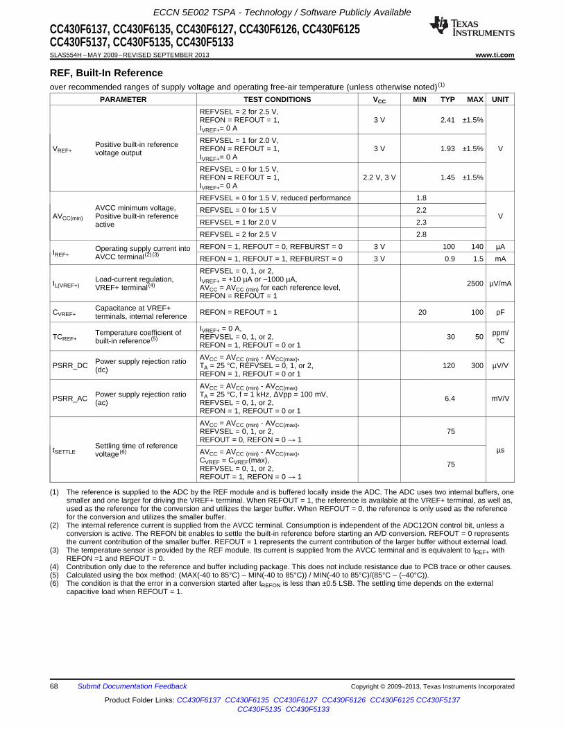
ECCN 5E002 TSPA - Technology / Software Publicly Available
CC430F6137, CC430F6135, CC430F6127, CC430F6126, CC430F6125CC430F5137, CC430F5135, CC430F5133SLAS554H –MAY 2009–REVISED SEPTEMBER 2013 www.ti.com
REF, Built-In Referenceover recommended ranges of supply voltage and operating free-air temperature (unless otherwise noted) (1)
PARAMETER TEST CONDITIONS VCC MIN TYP MAX UNITREFVSEL = 2 for 2.5 V,REFON = REFOUT = 1, 3 V 2.41 ±1.5%IVREF+= 0 AREFVSEL = 1 for 2.0 V,Positive built-in referenceVREF+ REFON = REFOUT = 1, 3 V 1.93 ±1.5% Vvoltage output IVREF+= 0 AREFVSEL = 0 for 1.5 V,REFON = REFOUT = 1, 2.2 V, 3 V 1.45 ±1.5%IVREF+= 0 AREFVSEL = 0 for 1.5 V, reduced performance 1.8
AVCC minimum voltage, REFVSEL = 0 for 1.5 V 2.2AVCC(min) Positive built-in reference V
REFVSEL = 1 for 2.0 V 2.3activeREFVSEL = 2 for 2.5 V 2.8REFON = 1, REFOUT = 0, REFBURST = 0 3 V 100 140 µAOperating supply current intoIREF+ AVCC terminal (2) (3) REFON = 1, REFOUT = 1, REFBURST = 0 3 V 0.9 1.5 mAREFVSEL = 0, 1, or 2,
Load-current regulation, IVREF+ = +10 µA or –1000 µA,IL(VREF+) 2500 µV/mAVREF+ terminal (4) AVCC = AVCC (min) for each reference level,REFON = REFOUT = 1
Capacitance at VREF+CVREF+ REFON = REFOUT = 1 20 100 pFterminals, internal referenceIVREF+ = 0 A,Temperature coefficient of ppm/TCREF+ REFVSEL = 0, 1, or 2, 30 50built-in reference (5) °CREFON = 1, REFOUT = 0 or 1AVCC = AVCC (min) - AVCC(max),Power supply rejection ratioPSRR_DC TA = 25 °C, REFVSEL = 0, 1, or 2, 120 300 µV/V(dc) REFON = 1, REFOUT = 0 or 1AVCC = AVCC (min) - AVCC(max)
Power supply rejection ratio TA = 25 °C, f = 1 kHz, ΔVpp = 100 mV,PSRR_AC 6.4 mV/V(ac) REFVSEL = 0, 1, or 2,REFON = 1, REFOUT = 0 or 1AVCC = AVCC (min) - AVCC(max),REFVSEL = 0, 1, or 2, 75REFOUT = 0, REFON = 0 → 1
Settling time of referencetSETTLE µsAVCC = AVCC (min) - AVCC(max),voltage (6)CVREF = CVREF(max), 75REFVSEL = 0, 1, or 2,REFOUT = 1, REFON = 0 → 1
(1) The reference is supplied to the ADC by the REF module and is buffered locally inside the ADC. The ADC uses two internal buffers, onesmaller and one larger for driving the VREF+ terminal. When REFOUT = 1, the reference is available at the VREF+ terminal, as well as,used as the reference for the conversion and utilizes the larger buffer. When REFOUT = 0, the reference is only used as the referencefor the conversion and utilizes the smaller buffer.
(2) The internal reference current is supplied from the AVCC terminal. Consumption is independent of the ADC12ON control bit, unless aconversion is active. The REFON bit enables to settle the built-in reference before starting an A/D conversion. REFOUT = 0 representsthe current contribution of the smaller buffer. REFOUT = 1 represents the current contribution of the larger buffer without external load.
(3) The temperature sensor is provided by the REF module. Its current is supplied from the AVCC terminal and is equivalent to IREF+ withREFON =1 and REFOUT = 0.
(4) Contribution only due to the reference and buffer including package. This does not include resistance due to PCB trace or other causes.(5) Calculated using the box method: (MAX(-40 to 85°C) – MIN(-40 to 85°C)) / MIN(-40 to 85°C)/(85°C – (–40°C)).(6) The condition is that the error in a conversion started after tREFON is less than ±0.5 LSB. The settling time depends on the external
capacitive load when REFOUT = 1.
68 Submit Documentation Feedback Copyright © 2009–2013, Texas Instruments Incorporated
Product Folder Links: CC430F6137 CC430F6135 CC430F6127 CC430F6126 CC430F6125 CC430F5137CC430F5135 CC430F5133

ECCN 5E002 TSPA - Technology / Software Publicly Available
CC430F6137, CC430F6135, CC430F6127, CC430F6126, CC430F6125CC430F5137, CC430F5135, CC430F5133
www.ti.com SLAS554H –MAY 2009–REVISED SEPTEMBER 2013
Comparator_Bover recommended ranges of supply voltage and operating free-air temperature (unless otherwise noted)
PARAMETER TEST CONDITIONS VCC MIN TYP MAX UNITVCC Supply voltage 1.8 3.6 V
1.8 V 40CBPWRMD = 00 2.2 V 30 50Comparator operating supply current
IAVCC_COMP into AVCC, Excludes reference 3.0 V 40 65 µAresistor ladder CBPWRMD = 01 2.2 V, 3 V 10 30
CBPWRMD = 10 2.2 V, 3 V 0.1 0.5Quiescent current of local referenceIAVCC_REF CBREFACC = 1, CBREFLx = 01 22 µAvoltage amplifier into AVCC
VIC Common mode input range 0 VCC-1 VCBPWRMD = 00 ±20 mV
VOFFSET Input offset voltageCBPWRMD = 01, 10 ±10 mV
CIN Input capacitance 5 pFON - switch closed 3 4 kΩ
RSIN Series input resistanceOFF - switch opened 30 MΩCBPWRMD = 00, CBF = 0 450 ns
tPD Propagation delay, response time CBPWRMD = 01, CBF = 0 600 nsCBPWRMD = 10, CBF = 0 50 µsCBPWRMD = 00, CBON = 1, 0.35 0.6 1.0 µsCBF = 1, CBFDLY = 00CBPWRMD = 00, CBON = 1, 0.6 1.0 1.8 µsCBF = 1, CBFDLY = 01
tPD,filter Propagation delay with filter activeCBPWRMD = 00, CBON = 1, 1.0 1.8 3.4 µsCBF = 1, CBFDLY = 10CBPWRMD = 00, CBON = 1, 1.8 3.4 6.5 µsCBF = 1, CBFDLY = 11CBON = 0 to CBON = 1,tEN_CMP Comparator enable time, settling time 1 2 µsCBPWRMD = 00, 01, 10
tEN_REF Resistor reference enable time CBON = 0 to CBON = 1 0.3 1.5 µsVIN = reference into resistor ladder,VCB_REF Reference voltage for a given tap VIN × (n+1) / 32 Vn = 0 to 31
Copyright © 2009–2013, Texas Instruments Incorporated Submit Documentation Feedback 69
Product Folder Links: CC430F6137 CC430F6135 CC430F6127 CC430F6126 CC430F6125 CC430F5137CC430F5135 CC430F5133
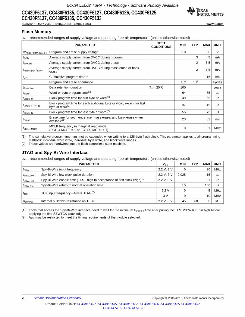
ECCN 5E002 TSPA - Technology / Software Publicly Available
CC430F6137, CC430F6135, CC430F6127, CC430F6126, CC430F6125CC430F5137, CC430F5135, CC430F5133SLAS554H –MAY 2009–REVISED SEPTEMBER 2013 www.ti.com
Flash Memoryover recommended ranges of supply voltage and operating free-air temperature (unless otherwise noted)
TESTPARAMETER MIN TYP MAX UNITCONDITIONSDVCC(PGM/ERASE) Program and erase supply voltage 1.8 3.6 VIPGM Average supply current from DVCC during program 3 5 mAIERASE Average supply current from DVCC during erase 2 6.5 mA
Average supply current from DVCC during mass erase or bankIMERASE, IBANK 2 6.5 mAerasetCPT Cumulative program time (1) 16 ms
Program and erase endurance 104 105 cyclestRetention Data retention duration TJ = 25°C 100 yearstWord Word or byte program time (2) 64 85 µstBlock, 0 Block program time for first byte or word (2) 49 65 µs
Block program time for each additional byte or word, except for lasttBlock, 1–(N–1) 37 49 µsbyte or word (2)
tBlock, N Block program time for last byte or word (2) 55 73 µsErase time for segment erase, mass erase, and bank erase whentErase 23 32 msavailable (2)
MCLK frequency in marginal read modefMCLK,MGR 0 1 MHz(FCTL4.MGR0 = 1 or FCTL4. MGR1 = 1)
(1) The cumulative program time must not be exceeded when writing to a 128-byte flash block. This parameter applies to all programmingmethods: individual word write, individual byte write, and block write modes.
(2) These values are hardwired into the flash controller's state machine.
JTAG and Spy-Bi-Wire Interfaceover recommended ranges of supply voltage and operating free-air temperature (unless otherwise noted)
PARAMETER VCC MIN TYP MAX UNITfSBW Spy-Bi-Wire input frequency 2.2 V, 3 V 0 20 MHztSBW,Low Spy-Bi-Wire low clock pulse duration 2.2 V, 3 V 0.025 15 µstSBW, En Spy-Bi-Wire enable time (TEST high to acceptance of first clock edge) (1) 2.2 V, 3 V 1 µstSBW,Rst Spy-Bi-Wire return to normal operation time 15 100 µs
2.2 V 0 5 MHzfTCK TCK input frequency - 4-wire JTAG (2)
3 V 0 10 MHzRinternal Internal pulldown resistance on TEST 2.2 V, 3 V 45 60 80 kΩ
(1) Tools that access the Spy-Bi-Wire interface need to wait for the minimum tSBW,En time after pulling the TEST/SBWTCK pin high beforeapplying the first SBWTCK clock edge.
(2) fTCK may be restricted to meet the timing requirements of the module selected.
70 Submit Documentation Feedback Copyright © 2009–2013, Texas Instruments Incorporated
Product Folder Links: CC430F6137 CC430F6135 CC430F6127 CC430F6126 CC430F6125 CC430F5137CC430F5135 CC430F5133

ECCN 5E002 TSPA - Technology / Software Publicly Available
CC430F6137, CC430F6135, CC430F6127, CC430F6126, CC430F6125CC430F5137, CC430F5135, CC430F5133
www.ti.com SLAS554H –MAY 2009–REVISED SEPTEMBER 2013
RF1A CC1101-Based Radio Parameters
Recommended Operating ConditionsPARAMETER TEST CONDITIONS MIN TYP MAX UNIT
VCC Supply voltage range during radio operation 2.0 3.6 VPMMCOREVx Core voltage range, PMMCOREVx setting during radio operation 2 3
300 348RF frequency range 389 (1) 464 MHz
779 9282-FSK 0.6 500
Data rate 2-GFSK, OOK, and ASK 0.6 250 kBaud(Shaped) MSK (also known as differential offset QPSK) (2) 26 500
RF crystal frequency 26 26 27 MHzRF crystal tolerance Total tolerance including initial tolerance, crystal loading, aging and ±40 ppm
temperature dependency. (3)
RF crystal load capacitance 10 13 20 pFRF crystal effective series 100 Ωresistance
(1) If using a 27-MHz crystal, the lower frequency limit for this band is 392 MHz.(2) If using optional Manchester encoding, the data rate in kbps is half the baud rate.(3) The acceptable crystal tolerance depends on frequency band, channel bandwidth, and spacing. Also see design note DN005 -- CC11xx
Sensitivity versus Frequency Offset and Crystal Accuracy (SWRA122).
RF Crystal Oscillator, XT2TA = 25°C, VCC = 3 V (unless otherwise noted) (1)
PARAMETER TEST CONDITIONS MIN TYP MAX UNITStart-up time (2) 150 810 µsDuty cycle 45 50 55 %
(1) All measurement results are obtained using the EM430F6137RF900 with BOM according to tested frequency range (see Table 48).(2) The start-up time depends to a very large degree on the used crystal.
Current Consumption, Reduced-Power ModesTA = 25°C, VCC = 3 V (unless otherwise noted) (1)
PARAMETER TEST CONDITIONS MIN TYP MAX UNITCurrent RF crystal oscillator only (for example, SLEEP state with MCSM0.OSC_FORCE_ON = 100 µAconsumption 1)
IDLE state (including RF crystal oscillator) 1.7 mAFSTXON state (only the frequency synthesizer is running) (2) 9.5 mA
(1) All measurement results are obtained using the EM430F6137RF900 with BOM according to tested frequency range (see Table 48).(2) This current consumption is also representative of other intermediate states when going from IDLE to RX or TX, including the calibration
state.
Copyright © 2009–2013, Texas Instruments Incorporated Submit Documentation Feedback 71
Product Folder Links: CC430F6137 CC430F6135 CC430F6127 CC430F6126 CC430F6125 CC430F5137CC430F5135 CC430F5133

ECCN 5E002 TSPA - Technology / Software Publicly Available
CC430F6137, CC430F6135, CC430F6127, CC430F6126, CC430F6125CC430F5137, CC430F5135, CC430F5133SLAS554H –MAY 2009–REVISED SEPTEMBER 2013 www.ti.com
Current Consumption, Receive ModeTA = 25°C, VCC = 3 V (unless otherwise noted) (1) (2)
DATAFREQPARAMETER RATE TEST CONDITIONS MIN TYP MAX UNIT(MHz) (kBaud)Input at -100 dBm (close to 17sensitivity limit)
1.2Input at -40 dBm (well above 16sensitivity limit)Input at -100 dBm (close to 17Register settings sensitivity limit)
315 38.4 optimized for reducedInput at -40 dBm (well abovecurrent 16sensitivity limit)Input at -100 dBm (close to 18sensitivity limit)
250Input at -40 dBm (well above 16.5sensitivity limit)Input at -100 dBm (close to 18sensitivity limit)
1.2Input at -40 dBm (well above 17sensitivity limit)Input at -100 dBm (close to 18Current Register settings sensitivity limit)
consumption, 433 38.4 optimized for reduced mAInput at -40 dBm (well aboveRX current 17sensitivity limit)Input at -100 dBm (close to 18.5sensitivity limit)
250Input at -40 dBm (well above 17sensitivity limit)Input at -100 dBm (close to 16sensitivity limit)
1.2Input at -40 dBm (well above 15sensitivity limit)Input at -100 dBm (close to 16Register settings sensitivity limit)
868, 915 38.4 optimized for reducedInput at -40 dBm (well abovecurrent (3) 15sensitivity limit)Input at -100 dBm (close to 16sensitivity limit)
250Input at -40 dBm (well above 15sensitivity limit)
(1) All measurement results are obtained using the EM430F6137RF900 with BOM according to tested frequency range (see Table 48).(2) Reduced current setting (MDMCFG2.DEM_DCFILT_OFF = 1) gives a slightly lower current consumption at the cost of a reduction in
sensitivity. See tables "RF Receive" for additional details on current consumption and sensitivity.(3) For 868 or 915 MHz, see Figure 21 for current consumption with register settings optimized for sensitivity.
72 Submit Documentation Feedback Copyright © 2009–2013, Texas Instruments Incorporated
Product Folder Links: CC430F6137 CC430F6135 CC430F6127 CC430F6126 CC430F6125 CC430F5137CC430F5135 CC430F5133

16
17
18
19
-100 -80 -60 -40 -20
Input Power [dBm]
Rad
ioC
urr
en
t[m
A]
TA = 85°C
TA = 25°C
TA = -40°C
16
17
18
19
-100 -80 -60 -40 -20
Input Power [dBm]
Rad
ioC
urr
en
t[m
A]
TA = 85°C
TA = 25°C
TA = -40°C
16
17
18
19
-100 -80 -60 -40 -20
Input Power [dBm]
Rad
ioC
urr
en
t[m
A]
TA = 85°C
TA = 25°C
TA = -40°C
16
17
18
19
-100 -80 -60 -40 -20
Input Power [dBm]
Rad
ioC
urr
en
t[m
A]
TA = 85°C
TA = 25°C
TA = -40°C
1.2 kBaud GFSK
250 kBaud GFSK
38.4 kBaud GFSK
500 kBaud MSK
ECCN 5E002 TSPA - Technology / Software Publicly Available
CC430F6137, CC430F6135, CC430F6127, CC430F6126, CC430F6125CC430F5137, CC430F5135, CC430F5133
www.ti.com SLAS554H –MAY 2009–REVISED SEPTEMBER 2013
Figure 21. Typical RX Current Consumption Over Temperature and Input Power Level, 868 MHz,Sensitivity-Optimized Setting
Copyright © 2009–2013, Texas Instruments Incorporated Submit Documentation Feedback 73
Product Folder Links: CC430F6137 CC430F6135 CC430F6127 CC430F6126 CC430F6125 CC430F5137CC430F5135 CC430F5133

ECCN 5E002 TSPA - Technology / Software Publicly Available
CC430F6137, CC430F6135, CC430F6127, CC430F6126, CC430F6125CC430F5137, CC430F5135, CC430F5133SLAS554H –MAY 2009–REVISED SEPTEMBER 2013 www.ti.com
Current Consumption, Transmit ModeTA = 25°C, VCC = 3 V (unless otherwise noted) (1) (2)
FREQUENCY PATABLE OUTPUTPARAMETER MIN TYP MAX UNIT[MHz Setting POWER (dBm)0xC0 max. 26 mA0xC4 +10 25 mA
3150x51 0 15 mA0x29 -6 15 mA0xC0 max. 33 mA0xC6 +10 29 mA
4330x50 0 17 mA0x2D -6 17 mA
Current consumption, TX0xC0 max. 36 mA0xC3 +10 33 mA
8680x8D 0 18 mA0x2D -6 18 mA0xC0 max. 35 mA0xC3 +10 32 mA
9150x8D 0 18 mA0x2D -6 18 mA
(1) All measurement results are obtained using the EM430F6137RF900 with BOM according to tested frequency range (see Table 48).(2) Reduced current setting (MDMCFG2.DEM_DCFILT_OFF = 1) gives a slightly lower current consumption at the cost of a reduction in
sensitivity. See tables "RF Receive" for additional details on current consumption and sensitivity.
74 Submit Documentation Feedback Copyright © 2009–2013, Texas Instruments Incorporated
Product Folder Links: CC430F6137 CC430F6135 CC430F6127 CC430F6126 CC430F6125 CC430F5137CC430F5135 CC430F5133

ECCN 5E002 TSPA - Technology / Software Publicly Available
CC430F6137, CC430F6135, CC430F6127, CC430F6126, CC430F6125CC430F5137, CC430F5135, CC430F5133
www.ti.com SLAS554H –MAY 2009–REVISED SEPTEMBER 2013
Typical TX Current Consumption, 315 MHzOutput VCC 2.0 V 3.0 V 3.6 VPATABLEPARAMETER Power UNITSetting TA 25°C 25°C 25°C(dBm)
0xC0 max. 27.5 26.4 28.1Current 0xC4 +10 25.1 25.2 25.3consumption, mA
0x51 0 14.4 14.6 14.7TX0x29 -6 14.2 14.7 15.0
Typical TX Current Consumption, 433 MHzOutput VCC 2.0 V 3.0 V 3.6 VPATABLEPARAMETER Power UNITSetting TA 25°C 25°C 25°C(dBm)
0xC0 max. 33.1 33.4 33.8Current 0xC6 +10 28.6 28.8 28.8consumption, mA
0x50 0 16.6 16.8 16.9TX0x2D -6 16.8 17.5 17.8
Typical TX Current Consumption, 868 MHzOutput VCC 2.0 V 3.0 V 3.6 VPATABLEPARAMETER Power UNITSetting TA -40°C 25°C 85°C -40°C 25°C 85°C -40°C 25°C 85°C(dBm)
0xC0 max. 36.7 35.2 34.2 38.5 35.5 34.9 37.1 35.7 34.7Current 0xC3 +10 34.0 32.8 32.0 34.2 33.0 32.5 34.3 33.1 32.2consumption, mA
0x8D 0 18.0 17.6 17.5 18.3 17.8 18.1 18.4 18.0 17.7TX0x2D -6 17.1 17.0 17.2 17.8 17.8 18.3 18.2 18.1 18.1
Typical TX Current Consumption, 915 MHzOutput VCC 2.0 V 3.0 V 3.6 VPATABLEPARAMETER Power UNITSetting TA -40°C 25°C 85°C -40°C 25°C 85°C -40°C 25°C 85°C(dBm)
0xC0 max. 35.5 33.8 33.2 36.2 34.8 33.6 36.3 35.0 33.8Current 0xC3 +10 33.2 32.0 31.0 33.4 32.1 31.2 33.5 32.3 31.3consumption, mA
0x8D 0 17.8 17.4 17.1 18.1 17.6 17.3 18.2 17.8 17.5TX0x2D -6 17.0 16.9 16.9 17.7 17.6 17.6 18.1 18.0 18.0
Copyright © 2009–2013, Texas Instruments Incorporated Submit Documentation Feedback 75
Product Folder Links: CC430F6137 CC430F6135 CC430F6127 CC430F6126 CC430F6125 CC430F5137CC430F5135 CC430F5133

ECCN 5E002 TSPA - Technology / Software Publicly Available
CC430F6137, CC430F6135, CC430F6127, CC430F6126, CC430F6125CC430F5137, CC430F5135, CC430F5133SLAS554H –MAY 2009–REVISED SEPTEMBER 2013 www.ti.com
RF Receive, OverallTA = 25°C, VCC = 3 V (unless otherwise noted) (1)
PARAMETER TEST CONDITIONS MIN TYP MAX UNITDigital channel filter bandwidth (2) 58 812 kHz
25 MHz to 1 GHz -68 -57Spurious emissions (3) (4) dBm
Above 1 GHz -66 -47RX latency Serial operation (5) 9 bit
(1) All measurement results are obtained using the EM430F6137RF900 with BOM according to tested frequency range (see Table 48).(2) User programmable. The bandwidth limits are proportional to crystal frequency (given values assume a 26.0 MHz crystal)(3) Typical radiated spurious emission is -49 dBm measured at the VCO frequency(4) Maximum figure is the ETSI EN 300 220 limit(5) Time from start of reception until data is available on the receiver data output pin is equal to 9 bit.
RF Receive, 315 MHzTA = 25°C, VCC = 3 V (unless otherwise noted) (1)
2-FSK, 1% packet error rate, 20-byte packet length, Sensitivity optimized, MDMCFG2.DEM_DCFILT_OFF = 0 (unlessotherwise noted)
DATA RATEPARAMETER TEST CONDITIONS MIN TYP MAX UNIT(kBaud)0.6 14.3kHz deviation, 58kHz digital channel filter bandwidth -1171.2 5.2kHz deviation, 58kHz digital channel filter bandwidth (2) -111
Receiver sensitivity 38.4 20kHz deviation, 100kHz digital channel filter bandwidth (3) -103 dBm250 127kHz deviation, 540kHz digital channel filter bandwidth (4) -95500 MSK, 812kHz digital channel filter bandwidth (4) -86
(1) All measurement results are obtained using the EM430F6137RF900 with BOM according to tested frequency range (see Table 48).(2) Sensitivity can be traded for current consumption by setting MDMCFG2.DEM_DCFILT_OFF=1. The typical current consumption is then
reduced by about 2mA close to the sensitivity limit. The sensitivity is typically reduced to -109dBm.(3) Sensitivity can be traded for current consumption by setting MDMCFG2.DEM_DCFILT_OFF=1. The typical current consumption is then
reduced by about 2mA close to the sensitivity limit. The sensitivity is typically reduced to -102dBm.(4) MDMCFG2.DEM_DCFILT_OFF=1 can not be used for data rates ≥ 250kBaud.
RF Receive, 433 MHzTA = 25°C, VCC = 3 V (unless otherwise noted) (1)
2-FSK, 1% packet error rate, 20-byte packet length, Sensitivity optimized, MDMCFG2.DEM_DCFILT_OFF = 0 (unlessotherwise noted)
DATA RATEPARAMETER TEST CONDITIONS MIN TYP MAX UNIT(kBaud)0.6 14.3kHz deviation, 58kHz digital channel filter bandwidth -1141.2 5.2-kHz deviation, 58-kHz digital channel filter bandwidth (2) -111
38.4 20-kHz deviation, 100-kHz digital channel filter bandwidth (3) -104Receiver sensitivity dBm127-kHz deviation, 540-kHz digital channel filter bandwidth250 -93(4)
500 MSK, 812kHz digital channel filter bandwidth (4) -85
(1) All measurement results are obtained using the EM430F6137RF900 with BOM according to tested frequency range (see Table 48).(2) Sensitivity can be traded for current consumption by setting MDMCFG2.DEM_DCFILT_OFF=1. The typical current consumption is then
reduced by about 2mA close to the sensitivity limit. The sensitivity is typically reduced to -109dBm.(3) Sensitivity can be traded for current consumption by setting MDMCFG2.DEM_DCFILT_OFF=1. The typical current consumption is then
reduced by about 2mA close to the sensitivity limit. The sensitivity is typically reduced to -101dBm.(4) MDMCFG2.DEM_DCFILT_OFF=1 can not be used for data rates ≥ 250kBaud.
76 Submit Documentation Feedback Copyright © 2009–2013, Texas Instruments Incorporated
Product Folder Links: CC430F6137 CC430F6135 CC430F6127 CC430F6126 CC430F6125 CC430F5137CC430F5135 CC430F5133

ECCN 5E002 TSPA - Technology / Software Publicly Available
CC430F6137, CC430F6135, CC430F6127, CC430F6126, CC430F6125CC430F5137, CC430F5135, CC430F5133
www.ti.com SLAS554H –MAY 2009–REVISED SEPTEMBER 2013
RF Receive, 868 or 915 MHzTA = 25°C, VCC = 3 V (unless otherwise noted) (1)
1% packet error rate, 20-byte packet length, Sensitivity optimized, MDMCFG2.DEM_DCFILT_OFF = 0 (unless otherwisenoted)PARAMETER TEST CONDITIONS MIN TYP MAX UNIT0.6-kBaud data rate, 2-FSK, 14.3-kHz deviation, 58-kHz digital channel filter bandwidth (unless otherwise noted)Receiver sensitivity -115 dBm1.2-kBaud data rate, 2-FSK, 5.2-kHz deviation, 58-kHz digital channel filter bandwidth (unless otherwise noted)
-109Receiver sensitivity (2) dBm2-GFSK modulation by setting MDMCFG2.MOD_FORMAT=2, -109Gaussian filter with BT = 0.5Saturation FIFOTHR.CLOSE_IN_RX=0 (3) -28 dBm
-100-kHz offset 39Adjacent channel Desired channel 3 dB above the sensitivity limit, dBrejection 100 kHz channel spacing (4) +100-kHz offset 39IF frequency 152 kHz, desired channel 3 dB aboveImage channel rejection 29 dBthe sensitivity limit
±2 MHz offset -48 dBmBlocking Desired channel 3 dB above the sensitivity limit (5)
±10 MHz offset -40 dBm38.4-kBaud data rate, 2-FSK, 20-kHz deviation, 100-kHz digital channel filter bandwidth (unless otherwise noted)Receiver sensitivity (6) -102
dBm2-GFSK modulation by setting MDMCFG2.MOD_FORMAT = 2, -101Gaussian filter with BT = 0.5Saturation FIFOTHR.CLOSE_IN_RX=0 (3) -19 dBmAdjacent channel Desired channel 3 dB above the sensitivity limit, -200-kHz offset 20
dBrejection 200 kHz channel spacing (5)+200-kHz offset 25
Image channel rejection IF frequency 152 kHz, Desired channel 3 dB above the sensitivity limit 23 dBBlocking Desired channel 3 dB above the sensitivity limit (5) ±2-MHz offset -48 dBm
±10-MHz offset -40 dBm250-kBaud data rate, 2-FSK, 127-kHz deviation, 540-kHz digital channel filter bandwidth (unless otherwise noted)Receiver sensitivity (7) -90
dBm2-GFSK modulation by setting MDMCFG2.MOD_FORMAT = 2, -90Gaussian filter with BT = 0.5Saturation FIFOTHR.CLOSE_IN_RX=0 (3) -19 dBmAdjacent channel Desired channel 3 dB above the sensitivity limit, -750-kHz offset 24
dBrejection 750-kHz channel spacing (8)+750-kHz offset 30
Image channel rejection IF frequency 304 kHz, Desired channel 3 dB above the sensitivity limit 18 dBBlocking Desired channel 3 dB above the sensitivity limit (8) ±2-MHz offset -53 dBm
±10-MHz offset -39 dBm500-kBaud data rate, MSK, 812-kHz digital channel filter bandwidth (unless otherwise noted)Receiver sensitivity (7) -84 dBmImage channel rejection IF frequency 355 kHz, Desired channel 3 dB above the sensitivity limit -2 dBBlocking Desired channel 3 dB above the sensitivity limit (9) ±2-MHz offset -53 dBm
±10-MHz offset -38 dBm
(1) All measurement results are obtained using the EM430F6137RF900 with BOM according to tested frequency range (see Table 48).(2) Sensitivity can be traded for current consumption by setting MDMCFG2.DEM_DCFILT_OFF=1. The typical current consumption is then
reduced by about 2mA close to the sensitivity limit. The sensitivity is typically reduced to -107dBm(3) See design note DN010 Close-in Reception with CC1101 (SWRA147).(4) See Figure 22 for blocking performance at other offset frequencies.(5) See Figure 23 for blocking performance at other offset frequencies.(6) Sensitivity can be traded for current consumption by setting MDMCFG2.DEM_DCFILT_OFF=1. The typical current consumption is then
reduced by about 2mA close to the sensitivity limit. The sensitivity is typically reduced to -100dBm.(7) MDMCFG2.DEM_DCFILT_OFF = 1 cannot be used for data rates ≥ 250kBaud.(8) See Figure 24 for blocking performance at other offset frequencies.(9) See Figure 25 for blocking performance at other offset frequencies.
Copyright © 2009–2013, Texas Instruments Incorporated Submit Documentation Feedback 77
Product Folder Links: CC430F6137 CC430F6135 CC430F6127 CC430F6126 CC430F6125 CC430F5137CC430F5135 CC430F5133

-20
-10
0
10
20
30
40
50
60
70
80
-40 -30 -20 -10 0 10 20 30 40
Offset [MHz]
Blo
ckin
g[d
B]
-20
-10
0
10
20
30
40
50
-1 -0.8 -0.6 -0.4 -0.2 0 0.2 0.4 0.6 0.8 1
Offset [MHz]
Sele
cti
vit
y[d
B]
-20
-10
0
10
20
30
40
50
60
70
80
-40 -30 -20 -10 0 10 20 30 40
Offset [MHz]
Blo
ckin
g[d
B]
-10
0
10
20
30
40
50
60
-1 -0.8 -0.6 -0.4 -0.2 0 0.2 0.4 0.6 0.8 1
Offset [MHz]
Sele
cti
vit
y[d
B]
ECCN 5E002 TSPA - Technology / Software Publicly Available
CC430F6137, CC430F6135, CC430F6127, CC430F6126, CC430F6125CC430F5137, CC430F5135, CC430F5133SLAS554H –MAY 2009–REVISED SEPTEMBER 2013 www.ti.com
NOTE: 868.3 MHz, 2-FSK, 5.2-kHz deviation, IF frequency is 152.3 kHz, digital channel filter bandwidth is 58 kHz
Figure 22. Typical Selectivity at 1.2-kBaud Data Rate
NOTE: 868 MHz, 2-FSK, 20 kHz deviation, IF frequency is 152.3 kHz, digital channel filter bandwidth is 100 kHz
Figure 23. Typical Selectivity at 38.4-kBaud Data Rate
78 Submit Documentation Feedback Copyright © 2009–2013, Texas Instruments Incorporated
Product Folder Links: CC430F6137 CC430F6135 CC430F6127 CC430F6126 CC430F6125 CC430F5137CC430F5135 CC430F5133

-20
-10
0
10
20
30
40
50
60
70
80
-40 -30 -20 -10 0 10 20 30 40
Offset [MHz]
Blo
ckin
g[d
B]
-20
-10
0
10
20
30
40
50
-3 -2 -1 0 1 2 3
Offset [MHz]
Sele
cti
vit
y[d
B]
-20
-10
0
10
20
30
40
50
60
70
80
-40 -30 -20 -10 0 10 20 30 40
Offset [MHz]
Blo
ckin
g[d
B]
-20
-10
0
10
20
30
40
50
-3 -2 -1 0 1 2 3
Offset [MHz]
Sele
cti
vit
y[d
B]
ECCN 5E002 TSPA - Technology / Software Publicly Available
CC430F6137, CC430F6135, CC430F6127, CC430F6126, CC430F6125CC430F5137, CC430F5135, CC430F5133
www.ti.com SLAS554H –MAY 2009–REVISED SEPTEMBER 2013
NOTE: 868 MHz, 2-FSK, IF frequency is 304 kHz, digital channel filter bandwidth is 540 kHz
Figure 24. Typical Selectivity at 250-kBaud Data Rate
NOTE: 868 MHz, 2-FSK, IF frequency is 355 kHz, digital channel filter bandwidth is 812 kHz
Figure 25. Typical Selectivity at 500-kBaud Data Rate
Copyright © 2009–2013, Texas Instruments Incorporated Submit Documentation Feedback 79
Product Folder Links: CC430F6137 CC430F6135 CC430F6127 CC430F6126 CC430F6125 CC430F5137CC430F5135 CC430F5133

ECCN 5E002 TSPA - Technology / Software Publicly Available
CC430F6137, CC430F6135, CC430F6127, CC430F6126, CC430F6125CC430F5137, CC430F5135, CC430F5133SLAS554H –MAY 2009–REVISED SEPTEMBER 2013 www.ti.com
Typical Sensitivity, 315 MHz, Sensitivity Optimized SettingVCC 2.0 V 3.0 V 3.6 V
PARAMETER DATA RATE (kBaud) UNITTA -40°C 25°C 85°C -40°C 25°C 85°C -40°C 25°C 85°C
1.2 -112 -112 -110 -112 -111 -109 -112 -111 -108Sensitivity, 38.4 -105 -105 -104 -105 -103 -102 -105 -104 -102 dBm315MHz
250 -95 -95 -92 -94 -95 -92 -95 -94 -91
Typical Sensitivity, 433 MHz, Sensitivity Optimized SettingVCC 2.0 V 3.0 V 3.6 V
PARAMETER DATA RATE (kBaud) UNITTA -40°C 25°C 85°C -40°C 25°C 85°C -40°C 25°C 85°C
1.2 -111 -110 -108 -111 -111 -108 -111 -110 -107Sensitivity, 38.4 -104 -104 -101 -104 -104 -101 -104 -103 -101 dBm433MHz
250 -93 -94 -91 -93 -93 -90 -93 -93 -90
Typical Sensitivity, 868 MHz, Sensitivity Optimized SettingVCC 2.0 V 3.0 V 3.6 V
PARAMETER DATA RATE (kBaud) UNITTA -40°C 25°C 85°C -40°C 25°C 85°C -40°C 25°C 85°C
1.2 -109 -109 -107 -109 -109 -106 -109 -108 -10638.4 -102 -102 -100 -102 -102 -99 -102 -101 -99Sensitivity, dBm868MHz 250 -90 -90 -88 -89 -90 -87 -89 -90 -87500 -84 -84 -81 -84 -84 -80 -84 -84 -80
Typical Sensitivity, 915 MHz, Sensitivity Optimized SettingVCC 2.0 V 3.0 V 3.6 V
PARAMETER DATA RATE (kBaud) UNITTA -40°C 25°C 85°C -40°C 25°C 85°C -40°C 25°C 85°C
1.2 -109 -109 -107 -109 -109 -106 -109 -108 -10538.4 -102 -102 -100 -102 -102 -99 -103 -102 -99Sensitivity, dBm915MHz 250 -92 -92 -89 -92 -92 -88 -92 -92 -88500 -87 -86 -81 -86 -86 -81 -86 -85 -80
80 Submit Documentation Feedback Copyright © 2009–2013, Texas Instruments Incorporated
Product Folder Links: CC430F6137 CC430F6135 CC430F6127 CC430F6126 CC430F6125 CC430F5137CC430F5135 CC430F5133

ECCN 5E002 TSPA - Technology / Software Publicly Available
CC430F6137, CC430F6135, CC430F6127, CC430F6126, CC430F6125CC430F5137, CC430F5135, CC430F5133
www.ti.com SLAS554H –MAY 2009–REVISED SEPTEMBER 2013
RF TransmitTA = 25°C, VCC = 3 V (unless otherwise noted) (1)
PTX = +10 dBm (unless otherwise noted)FREQUENCYPARAMETER TEST CONDITIONS MIN TYP MAX UNIT(MHz)
315 122 + j31Differential load 433 116 + j41 Ωimpedance (2)
868, 915 86.5 + j43315 +12433 +13Output power, highest Delivered to a 50Ω single-ended load via CC430 dBmsetting (3) reference design's RF matching network868 +11915 +11
Output power, lowest Delivered to a 50Ω single-ended load via CC430 -30 dBmsetting (3) reference design's RF matching networkSecond harmonic -56
433Third harmonic -57Second harmonic -50Harmonics, 868 dBmradiated (4) (5) (6) Third harmonic -52Second harmonic -50
915Third harmonic -54Frequencies below 960 MHz < -38
315 +10 dBm CWFrequencies above 960 MHz < -48Frequencies below 1 GHz -45
433 +10 dBm CWFrequencies above 1 GHz < -48
Harmonics, conducted dBmSecond harmonic -59
868 +10 dBm CWOther harmonics < -71Second harmonic -53
915 +11 dBm CW (7)Other harmonics < -47Frequencies below 960 MHz < -58
315 +10 dBm CWFrequencies above 960 MHz < -53Frequencies below 1 GHz < -54Frequencies above 1 GHz < -54433 +10 dBm CWFrequencies within 47 to 74, 87.5 to < -63Spurious emissions, 118, 174 to 230, 470 to 862 MHz
conducted, harmonics dBmFrequencies below 1 GHz < -46not included (8)
Frequencies above 1 GHz < -59868 +10 dBm CWFrequencies within 47 to 74, 87.5 to < -56118, 174 to 230, 470 to 862 MHzFrequencies below 960 MHz < -49
915 +11 dBm CWFrequencies above 960 MHz < -63
(1) All measurement results are obtained using the EM430F6137RF900 with BOM according to tested frequency range (see Table 48).(2) Differential impedance as seen from the RF-port (RF_P and RF_N) towards the antenna. Follow the CC430 reference designs available
from the TI website.(3) Output power is programmable, and full range is available in all frequency bands. Output power may be restricted by regulatory limits.
See also application note AN050 Using the CC1101 in the European 868MHz SRD Band (SWRA146) and design note DN013Programming Output Power on CC1101 (SWRA168), which gives the output power and harmonics when using multi-layer inductors.The output power is then typically +10 dBm when operating at 868 or 915 MHz.
(4) The antennas used during the radiated measurements (SMAFF-433 from R.W.Badland and Nearson S331 868/915) play a part inattenuating the harmonics.
(5) Measured on EM430F6137RF900 with CW, maximum output power(6) All harmonics are below -41.2 dBm when operating in the 902 to 928 MHz band.(7) Requirement is -20 dBc under FCC 15.247(8) All radiated spurious emissions are within the limits of ETSI. Also see design note DN017 CC11xx 868/915 MHz RF Matching
(SWRA168).
Copyright © 2009–2013, Texas Instruments Incorporated Submit Documentation Feedback 81
Product Folder Links: CC430F6137 CC430F6135 CC430F6127 CC430F6126 CC430F6125 CC430F5137CC430F5135 CC430F5133

ECCN 5E002 TSPA - Technology / Software Publicly Available
CC430F6137, CC430F6135, CC430F6127, CC430F6126, CC430F6125CC430F5137, CC430F5135, CC430F5133SLAS554H –MAY 2009–REVISED SEPTEMBER 2013 www.ti.com
RF Transmit (continued)TA = 25°C, VCC = 3 V (unless otherwise noted)(1)
PTX = +10 dBm (unless otherwise noted)FREQUENCYPARAMETER TEST CONDITIONS MIN TYP MAX UNIT(MHz)
TX latency (9) Serial operation 8 bits
(9) Time from sampling the data on the transmitter data input pin until it is observed on the RF output ports
Optimum PATABLE Settings for Various Output Power Levels and Frequency BandsTA = 25°C, VCC = 3 V (unless otherwise noted) (1)
PATABLE SettingOutput Power (dBm)
315 MHz 433 MHz 868 MHz 915 MHz-30 0x12 0x05 0x03 0x03-12 0x33 0x26 0x25 0x25-6 0x29 0x2D 0x2D 0x2D0 0x51 0x50 0x8D 0x8D10 0xC4 0xC4 0xC3 0xC3
Maximum 0xC0 0xC0 0xC0 0xC0
(1) All measurement results are obtained using the EM430F6137RF900 with BOM according to tested frequency range (see Table 48).
82 Submit Documentation Feedback Copyright © 2009–2013, Texas Instruments Incorporated
Product Folder Links: CC430F6137 CC430F6135 CC430F6127 CC430F6126 CC430F6125 CC430F5137CC430F5135 CC430F5133

ECCN 5E002 TSPA - Technology / Software Publicly Available
CC430F6137, CC430F6135, CC430F6127, CC430F6126, CC430F6125CC430F5137, CC430F5135, CC430F5133
www.ti.com SLAS554H –MAY 2009–REVISED SEPTEMBER 2013
Typical Output Power, 315 MHz (1)
VCC 2.0 V 3.0 V 3.6 VPARAMETER PATABLE Setting UNIT
TA -40°C 25°C 85°C -40°C 25°C 85°C -40°C 25°C 85°C0xC0 (max) 11.9 11.8 11.80xC4 (10 dBm) 10.3 10.3 10.3
Output power, 0xC6 (default) 9.3 dBm315 MHz0x51 (0 dBm) 0.7 0.6 0.70x29 (-6 dBm) -6.8 -5.6 -5.3
(1) All measurement results are obtained using the EM430F6137RF900 with BOM according to tested frequency range (see Table 48).
Typical Output Power, 433 MHz (1)
VCC 2.0 V 3.0 V 3.6 VPARAMETER PATABLE Setting UNIT
TA -40°C 25°C 85°C -40°C 25°C 85°C -40°C 25°C 85°C0xC0 (max) 12.6 12.6 12.60xC4 (10 dBm) 10.3 10.2 10.2
Output power, 0xC6 (default) 10.0 dBm433 MHz0x50 (0 dBm) 0.3 0.3 0.30x2D (-6 dBm) -6.4 -5.4 -5.1
(1) All measurement results are obtained using the EM430F6137RF900 with BOM according to tested frequency range (see Table 48).
Typical Output Power, 868 MHz (1)
VCC 2.0 V 3.0 V 3.6 VPARAMETER PATABLE Setting UNIT
TA -40°C 25°C 85°C -40°C 25°C 85°C -40°C 25°C 85°C0xC0 (max) 11.9 11.2 10.5 11.9 11.2 10.5 11.9 11.2 10.50xC3 (10 dBm) 10.8 10.1 9.4 10.8 10.1 9.4 10.7 10.1 9.4
Output power, 0xC6 (default) 8.8 dBm868 MHz0x8D (0 dBm) 1.0 0.3 -0.3 1.1 0.3 -0.3 1.1 0.3 -0.30x2D (-6 dBm) -6.5 -6.8 -7.3 -5.3 -5.8 -6.3 -4.9 -5.4 -6.0
(1) All measurement results are obtained using the EM430F6137RF900 with BOM according to tested frequency range (see Table 48).
Typical Output Power, 915 MHz (1)
VCC 2.0 V 3.0 V 3.6 VPARAMETER PATABLE Setting UNIT
TA -40°C 25°C 85°C -40°C 25°C 85°C -40°C 25°C 85°C0xC0 (max) 12.2 11.4 10.6 12.1 11.4 10.7 12.1 11.4 10.70xC3 (10 dBm) 11.0 10.3 9.5 11.0 10.3 9.5 11.0 10.3 9.6
Output power, 0xC6 (default) 8.8 dBm915 MHz0x8D (0 dBm) 1.9 1.0 0.3 1.9 1.0 0.3 1.9 1.1 0.30x2D (-6 dBm) -5.5 -6.0 -6.5 -4.3 -4.8 -5.5 -3.9 -4.4 -5.1
(1) All measurement results are obtained using the EM430F6137RF900 with BOM according to tested frequency range (see Table 48).
Copyright © 2009–2013, Texas Instruments Incorporated Submit Documentation Feedback 83
Product Folder Links: CC430F6137 CC430F6135 CC430F6127 CC430F6126 CC430F6125 CC430F5137CC430F5135 CC430F5133
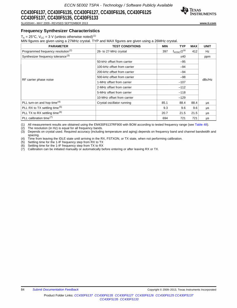
ECCN 5E002 TSPA - Technology / Software Publicly Available
CC430F6137, CC430F6135, CC430F6127, CC430F6126, CC430F6125CC430F5137, CC430F5135, CC430F5133SLAS554H –MAY 2009–REVISED SEPTEMBER 2013 www.ti.com
Frequency Synthesizer CharacteristicsTA = 25°C, VCC = 3 V (unless otherwise noted) (1)
MIN figures are given using a 27MHz crystal. TYP and MAX figures are given using a 26MHz crystal.PARAMETER TEST CONDITIONS MIN TYP MAX UNIT
Programmed frequency resolution (2) 26- to 27-MHz crystal 397 fXOSC/216 412 HzSynthesizer frequency tolerance (3) ±40 ppm
50-kHz offset from carrier –95100-kHz offset from carrier –94200-kHz offset from carrier –94500-kHz offset from carrier –98
RF carrier phase noise dBc/Hz1-MHz offset from carrier –1072-MHz offset from carrier –1125-MHz offset from carrier –11810-MHz offset from carrier –129
PLL turn-on and hop time (4) Crystal oscillator running 85.1 88.4 88.4 µsPLL RX to TX settling time (5) 9.3 9.6 9.6 µsPLL TX to RX settling time (6) 20.7 21.5 21.5 µsPLL calibration time (7) 694 721 721 µs
(1) All measurement results are obtained using the EM430F6137RF900 with BOM according to tested frequency range (see Table 48).(2) The resolution (in Hz) is equal for all frequency bands.(3) Depends on crystal used. Required accuracy (including temperature and aging) depends on frequency band and channel bandwidth and
spacing.(4) Time from leaving the IDLE state until arriving in the RX, FSTXON, or TX state, when not performing calibration.(5) Settling time for the 1-IF frequency step from RX to TX(6) Settling time for the 1-IF frequency step from TX to RX(7) Calibration can be initiated manually or automatically before entering or after leaving RX or TX.
84 Submit Documentation Feedback Copyright © 2009–2013, Texas Instruments Incorporated
Product Folder Links: CC430F6137 CC430F6135 CC430F6127 CC430F6126 CC430F6125 CC430F5137CC430F5135 CC430F5133

-120
-100
-80
-60
-40
-20
0
-120 -100 -80 -60 -40 -20 0
Input Power [dBm]
RS
SIR
ead
ou
t[d
Bm
]
1.2kBaud
38.4kBaud
-120
-100
-80
-60
-40
-20
0
-120 -100 -80 -60 -40 -20 0
Input Power [dBm]
RS
SIR
ead
ou
t[d
Bm
]
250kBaud
500kBaud
ECCN 5E002 TSPA - Technology / Software Publicly Available
CC430F6137, CC430F6135, CC430F6127, CC430F6126, CC430F6125CC430F5137, CC430F5135, CC430F5133
www.ti.com SLAS554H –MAY 2009–REVISED SEPTEMBER 2013
Typical RSSI_offset ValuesTA = 25°C, VCC = 3 V (unless otherwise noted) (1)
RSSI_OFFSET (dB)DATA RATE (kBaud)
433 MHz 868 MHz1.2 74 7438.4 74 74250 74 74500 74 74
(1) All measurement results are obtained using the EM430F6137RF900 with BOM according to tested frequency range (see Table 48).
Figure 26. Typical RSSI Value vs Input Power Level for Different Data Rates at 868 MHz
Copyright © 2009–2013, Texas Instruments Incorporated Submit Documentation Feedback 85
Product Folder Links: CC430F6137 CC430F6135 CC430F6127 CC430F6126 CC430F6125 CC430F5137CC430F5135 CC430F5133

RF
_N
RF
_P
AV
CC
_R
F
AV
CC
_R
F
AV
CC
_R
F
AV
CC
_R
F
GU
AR
D
C5
C6
C7
C3
C2
C1
C4
R1
C23
L1
L6
L5
L4
L3
L2
C29
C28
C27
C24
C25
C26
L7
SM
AS
TR
AIG
HT
JA
CK
, S
MT
R_
BIA
S
26M
Hz
C22
C21
RF
_X
OU
T
RF
_X
IN
VD
D
C9
C8
DVCC
VD
D C11
C10
C19
DV
CC
VC
OR
E
TD
O
TD
I/T
CL
K
TM
S
(JTA
G /
SB
W s
ign
als
)
AV
DD
C16
C17
C18
VD
D
C14
C15
R2
C20
DVCC
nRST/NMI/SBWTDIO
TCK
TEST/SBWTCK
AV
DD
C12
C13 AVCC
AVSS
(Ma
y b
e a
dd
ed
clo
se
to
th
e r
esp
ective
pin
sto
red
uce
em
issio
ns
at
5G
Hz
tole
ve
lsre
qu
ire
d b
y E
TS
I.)
CC
430F
61xx
17
64
18
63
19
62
20
61
21
60
22
59
29
52
30
51
31
50
32
49
23
58
24
57
25
56
26
55
27
54
28
53
33
16
34
15
35
14
36
13
37
12
38
11
45
4
46
3
47
2
48
1
39
10
40
9
41
8
42
7
43
6
44
5
ECCN 5E002 TSPA - Technology / Software Publicly Available
CC430F6137, CC430F6135, CC430F6127, CC430F6126, CC430F6125CC430F5137, CC430F5135, CC430F5133SLAS554H –MAY 2009–REVISED SEPTEMBER 2013 www.ti.com
APPLICATION CIRCUIT
For a complete reference design including layout see the CC430 Wireless Development Tools and relateddocumentation [MSP430 Hardware Tools User's Guide (SLAU278)].
Figure 27. Typical Application Circuit CC430F61xx
86 Submit Documentation Feedback Copyright © 2009–2013, Texas Instruments Incorporated
Product Folder Links: CC430F6137 CC430F6135 CC430F6127 CC430F6126 CC430F6125 CC430F5137CC430F5135 CC430F5133

RF
_N
RF
_P
AV
CC
_R
F
AV
CC
_R
F
AV
CC
_R
F
AV
CC
_R
F
GU
AR
D
C5
C6
C7
C3
C2
C1
C4
R1
C2
3
L1
L6
L5
L4
L3
L2
C2
9
C2
8
C2
7
C2
4
C2
5
C2
6
L7
SM
AS
TR
AIG
HT
JA
CK
, S
MT
R_B
IAS
26
MH
z
C2
2C
21
RF
_X
OU
T
RF
_X
IN
VD
D
C9
C8
DVCC
VD
D C11
C1
0
C1
9D
VC
C
VC
OR
E
TD
O
TD
I/T
CLK
(JTA
G / S
BW
sig
nals
)
AV
DD
C1
6
C1
7
C1
8
VD
D
C1
4
C1
5R
2
C2
0
DVCC
nRST/NMI/SBWTDIO
TCK
TEST/SBWTCK
AV
DD
C1
2
C1
3 AVCC
TMS
AVSS
12
114321 1098765
13
14
15
16
17
18
19
20
21
22
23
242
5
26
27
28
29
30
31
32
33
34
35
36
48
47
46
45
44
43
42
41
40
39
38
37
CC
43
0F
51
xx
(May b
e a
dded c
lose to the r
espective p
ins
tore
duce
em
issio
ns
at
5G
Hz
tole
vels
required b
y E
TS
I.)
ECCN 5E002 TSPA - Technology / Software Publicly Available
CC430F6137, CC430F6135, CC430F6127, CC430F6126, CC430F6125CC430F5137, CC430F5135, CC430F5133
www.ti.com SLAS554H –MAY 2009–REVISED SEPTEMBER 2013
For a complete reference design including layout see the CC430 Wireless Development Tools and relateddocumentation [MSP430 Hardware Tools User's Guide (SLAU278)].
Figure 28. Typical Application Circuit CC430F51xx
Copyright © 2009–2013, Texas Instruments Incorporated Submit Documentation Feedback 87
Product Folder Links: CC430F6137 CC430F6135 CC430F6127 CC430F6126 CC430F6125 CC430F5137CC430F5135 CC430F5133

ECCN 5E002 TSPA - Technology / Software Publicly Available
CC430F6137, CC430F6135, CC430F6127, CC430F6126, CC430F6125CC430F5137, CC430F5135, CC430F5133SLAS554H –MAY 2009–REVISED SEPTEMBER 2013 www.ti.com
Table 48. Bill of MaterialsComponents For 315 MHz For 433 MHz For 868, 915 MHz Comment
C1,3,4,5,7,9,11,13,15 100 nF Decoupling capacitorsC8,10,12,14 10 µF Decoupling capacitors
C2,6,16,17,18 2 pF Decoupling capacitorsC19 470 nF VCORE capacitor
RST decoupling capC20 2.2 nF (optimized for SBW)Load capacitors forC21,22 27 pF 26 MHz crystal (1)
R1 56 kΩ R_BIAS (±1% required)R2 47 kΩ RST pullup
L1,2 Capacitors: 220 pF 0.016 µH 0.012 µHL3,4 0.033 µH 0.027 µH 0.018 µHL5 0.033 µH 0.047 µH 0.015 µHL6 dnp (2) dnp (2) 0.0022 µHL7 0.033 µH 0.051 µH 0.015 µH
C23 dnp (2) 2.7 pF 1 pFC24 220 pF 220 pF 100 pFC25 6.8 pF 3.9 pF 1.5 pFC26 6.8 pF 3.9 pF 1.5 pFC27 220 pF 220 pF 1.5 pFC28 10 pF 4.7 pF 8.2 pFC29 220 pF 220 pF 1.5 pF
(1) The load capacitance CL seen by the crystal is CL = 1/((1/C21)+(1/C22)) + Cparasitic. The parasitic capacitance Cparasitic includes pincapacitance and PCB stray capacitance. It can be typically estimated to be approximately 2.5 pF.
(2) dnp = do not populate
88 Submit Documentation Feedback Copyright © 2009–2013, Texas Instruments Incorporated
Product Folder Links: CC430F6137 CC430F6135 CC430F6127 CC430F6126 CC430F6125 CC430F5137CC430F5135 CC430F5133

P1.0/P1MAP0(/S18)
P1.1/P1MAP1(/S19)
P1.2/P1MAP2(/S20)
P1.3/P1MAP3(/S21)
P1.4/P1MAP4(/S22)
Direction
0: Input
1: Output
P1SEL.x
1
0P1DIR.x
P1IN.x
P1IRQ.x
EN
to Port Mapping
1
0
from Port Mapping
P1OUT.x
Interrupt
Select
Edge
Q
EN
Set
P1 .SEL x
P1IES x.
P1IFG.x
P1IE.x
1
0DVSS
DVCC 1
P1DS.x
0: Low drive
1: High drive
D
from Port Mapping
S18...S22
LCDS18...LCDS22
Pad Logic
P1REN.x
P1MAP.x = PMAP_ANALOG
Bus
Keeper
(n/a CC430F513x)
ECCN 5E002 TSPA - Technology / Software Publicly Available
CC430F6137, CC430F6135, CC430F6127, CC430F6126, CC430F6125CC430F5137, CC430F5135, CC430F5133
www.ti.com SLAS554H –MAY 2009–REVISED SEPTEMBER 2013
INPUT/OUTPUT SCHEMATICS
Port P1, P1.0 to P1.4, Input/Output With Schmitt Trigger
CC430F513x devices don't provide LCD functionality on port P1 pins.
Copyright © 2009–2013, Texas Instruments Incorporated Submit Documentation Feedback 89
Product Folder Links: CC430F6137 CC430F6135 CC430F6127 CC430F6126 CC430F6125 CC430F5137CC430F5135 CC430F5133

ECCN 5E002 TSPA - Technology / Software Publicly Available
CC430F6137, CC430F6135, CC430F6127, CC430F6126, CC430F6125CC430F5137, CC430F5135, CC430F5133SLAS554H –MAY 2009–REVISED SEPTEMBER 2013 www.ti.com
Table 49. Port P1 (P1.0 to P1.4) Pin FunctionsCONTROL BITS/SIGNALS (1)
PIN NAME (P1.x) x FUNCTION LCDS19...P1DIR.x P1SEL.x P1MAPx 22 (2)
P1.0/P1MAP/S18 0 P1.0 (I/O) I: 0; O: 1 0 X 0Mapped secondary digital function - see Table 9 0; 1 (3) 1 ≤ 30 (3) 0Output driver and input Schmitt trigger disabled X 1 = 31 0S18 (not available on CC430F513x) X X X 1
P1.1/P1MAP1/S19 1 P1.1 (I/O) I: 0; O: 1 0 X 0Mapped secondary digital function - see Table 9 0; 1 (3) 1 ≤ 30 (3) 0Output driver and input Schmitt trigger disabled X 1 = 31 0S19 (not available on CC430F513x) X X X 1
P1.2/P1MAP2/S20 2 P1.2 (I/O) I: 0; O: 1 0 X 0Mapped secondary digital function - see Table 9 0; 1 (3) 1 ≤ 30 (3) 0Output driver and input Schmitt trigger disabled X 1 = 31 0S22 (not available on CC430F513x) X X X 1
P1.3/P1MAP3/S21 3 P1.3 (I/O) I: 0; O: 1 0 X 0Mapped secondary digital function - see Table 9 0; 1 (3) 1 ≤ 30 (3) 0Output driver and input Schmitt trigger disabled X 1 = 31 0S21 (not available on CC430F513x) X X X 1
P1.4/P1MAP4/S22 4 P1.4 (I/O) I: 0; O: 1 0 X 0Mapped secondary digital function - see Table 9 0; 1 (3) 1 ≤ 30 (3) 0Output driver and input Schmitt trigger disabled X 1 = 31 0S22 (not available on CC430F513x) X X X 1
(1) X = don't care(2) LCDSx not available in CC430F513x.(3) According to mapped function - see Table 9.
90 Submit Documentation Feedback Copyright © 2009–2013, Texas Instruments Incorporated
Product Folder Links: CC430F6137 CC430F6135 CC430F6127 CC430F6126 CC430F6125 CC430F5137CC430F5135 CC430F5133

P1.5/P1MAP5(/R23)
P1.6/P1MAP6(/R13)
P1.7/P1MAP7(/R03)P1SEL.x
1
0P1DIR.x
P1IN.x
P1IRQ.x
EN
to Port Mapping
1
0
from Port Mapping
P1OUT.x
Interrupt
Edge
Select
Q
EN
Set
P1SEL.x
P1IES.x
P1IFG.x
P1IE.x
1
0DVSS
DVCC 1
P1DS.x
0: Low drive
1: High drive
D
from Port Mapping
to LCD_B
Pad Logic
Bus
Keeper
Direction
0: Input
1: Output
P1REN.x
P1MAP.x = PMAP_ANALOG
(n/a CC430F513x)
ECCN 5E002 TSPA - Technology / Software Publicly Available
CC430F6137, CC430F6135, CC430F6127, CC430F6126, CC430F6125CC430F5137, CC430F5135, CC430F5133
www.ti.com SLAS554H –MAY 2009–REVISED SEPTEMBER 2013
Port P1, P1.5 to P1.7, Input/Output With Schmitt Trigger
CC430F513x devices don't provide LCD functionality on port P1 pins.
Table 50. Port P1 (P1.5 to P1.7) Pin FunctionsCONTROL BITS/SIGNALS (1)
PIN NAME (P1.x) x FUNCTIONP1DIR.x P1SEL.x P1MAPx
P1.5/P1MAP5/R23 5 P1.5 (I/O) I: 0; O: 1 0 XMapped secondary digital function - see Table 9 0; 1 (2) 1 ≤ 30 (2)
R23 (3) (not available on CC430F513x) X 1 = 31P1.6/P1MAP6/R13/ 6 P1.6 (I/O) I: 0; O: 1 0 XLCDREF Mapped secondary digital function - see Table 9 0; 1 (2) 1 ≤ 30 (2)
R13/LCDREF (3) (not available on CC430F513x) X 1 = 31P1.7/P1MAP7/R03 7 P1.7 (I/O) I: 0; O: 1 0 X
Mapped secondary digital function - see Table 9 0; 1 (2) 1 ≤ 30 (2)
R03 (3) (not available on CC430F513x) X 1 = 31
(1) X = don't care(2) According to mapped function - see Table 9.(3) Setting P1SEL.x bit together with P1MAPx = PM_ANALOG disables the output driver as well as the input Schmitt trigger.
Copyright © 2009–2013, Texas Instruments Incorporated Submit Documentation Feedback 91
Product Folder Links: CC430F6137 CC430F6135 CC430F6127 CC430F6126 CC430F6125 CC430F5137CC430F5135 CC430F5133

P2.0/P2MAP0/CB0(/A0)
P2.1/P2MAP2/CB1(/A1)
P2.2/P2MAP2/CB2(/A2)
P2.3/P2MAP3/CB3(/A3)
Direction
0: Input
1: Output
P2SEL.x
1
0P2DIR.x
P2IN.x
P2IRQ.x
EN
to Port Mapping
1
0
from Port Mapping
P2OUT.x
Interrupt
Select
Edge
Q
EN
Set
P2 .SEL x
P2IES x.
P2IFG.x
P2IE.x
1
0DVSS
DVCC 1
P2DS.x
0: Low drive
1: High drive
D
from Port Mapping
To Comparator_B
from Comparator_B
Pad Logic
To ADC12
INCHx = x
(n/a CC430F612x)
CBPD.x
P2REN.x
P2MAP.x = PMAP_ANALOG
Bus
Keeper
ECCN 5E002 TSPA - Technology / Software Publicly Available
CC430F6137, CC430F6135, CC430F6127, CC430F6126, CC430F6125CC430F5137, CC430F5135, CC430F5133SLAS554H –MAY 2009–REVISED SEPTEMBER 2013 www.ti.com
Port P2, P2.0 to P2.3, Input/Output With Schmitt Trigger
92 Submit Documentation Feedback Copyright © 2009–2013, Texas Instruments Incorporated
Product Folder Links: CC430F6137 CC430F6135 CC430F6127 CC430F6126 CC430F6125 CC430F5137CC430F5135 CC430F5133

P2.4/P2MAP4/CB4(/A4/VREF-/VeREF-)
P2.5/P2MAP5/CB5(/A5/VREF+/VeRF+)P2SEL.x
1
0P2DIR.x
P2IN.x
P2IRQ.x
EN
to Port Mapping
1
0
from Port Mapping
P2OUT.x
Interrupt
Select
Edge
Q
EN
Set
P2 .SEL x
P2IES x.
P2IFG.x
P2IE.x
1
0DVSS
DVCC 1
P2DS.x
0: Low drive
1: High drive
D
from Port Mapping
To Comparator_B
from Comparator_B
Pad Logic
To ADC12
INCHx = x
(n/a CC430F612x)
Bus
Keeper
to/from Reference
(n/a CC430F612x)
Direction
0: Input
1: Output
CBPD.x
P2REN.x
P2MAP.x = PMAP_ANALOG
ECCN 5E002 TSPA - Technology / Software Publicly Available
CC430F6137, CC430F6135, CC430F6127, CC430F6126, CC430F6125CC430F5137, CC430F5135, CC430F5133
www.ti.com SLAS554H –MAY 2009–REVISED SEPTEMBER 2013
Port P2, P2.4 to P2.5, Input/Output With Schmitt Trigger
Copyright © 2009–2013, Texas Instruments Incorporated Submit Documentation Feedback 93
Product Folder Links: CC430F6137 CC430F6135 CC430F6127 CC430F6126 CC430F6125 CC430F5137CC430F5135 CC430F5133

P2.6/P2MAP6(/CB6/A6)
P2.7/P2MAP7(/CB7/A7)
Direction
0: Input
1: Output
P2SEL.x
1
0P2DIR.x
P2IN.x
P2IRQ.x
EN
to Port Mapping
1
0
from Port Mapping
P2OUT.x
Interrupt
Select
Edge
Q
EN
Set
P2 .SEL x
P2IES x.
P2IFG.x
P2IE.x
1
0DVSS
DVCC 1
P2DS.x
0: Low drive
1: High drive
D
from Port Mapping
To Comparator_B
from Comparator_B
Pad Logic
To ADC12
INCHx = x
(n/a CC430F513x)
(n/a CC430F513x)
(n/a CC430F513x)CBPD.x
P2REN.x
P2MAP.x = PMAP_ANALOG
Bus
Keeper
ECCN 5E002 TSPA - Technology / Software Publicly Available
CC430F6137, CC430F6135, CC430F6127, CC430F6126, CC430F6125CC430F5137, CC430F5135, CC430F5133SLAS554H –MAY 2009–REVISED SEPTEMBER 2013 www.ti.com
Port P2, P2.6 and P2.7, Input/Output With Schmitt Trigger
CC430F513x devices don't provide analog functionality on port P2.6 and P2.7 pins.
94 Submit Documentation Feedback Copyright © 2009–2013, Texas Instruments Incorporated
Product Folder Links: CC430F6137 CC430F6135 CC430F6127 CC430F6126 CC430F6125 CC430F5137CC430F5135 CC430F5133

ECCN 5E002 TSPA - Technology / Software Publicly Available
CC430F6137, CC430F6135, CC430F6127, CC430F6126, CC430F6125CC430F5137, CC430F5135, CC430F5133
www.ti.com SLAS554H –MAY 2009–REVISED SEPTEMBER 2013
Table 51. Port P2 (P2.0 to P2.7) Pin FunctionsCONTROL BITS/SIGNALS (1)
PIN NAME (P2.x) x FUNCTIONP2DIR.x P2SEL.x P2MAPx CBPD.x
P2.0/P2MAP0/CB0 0 P2.0 (I/O) I: 0; O: 1 0 X 0(/A0) Mapped secondary digital function - see Table 9 0; 1 (2) 1 ≤ 30 (2) 0
A0 (not available on CC430F612x) (3) X 1 = 31 XCB0 (4) X X X 1
P2.1/P2MAP1/CB1 1 P2.1 (I/O) I: 0; O: 1 0 X 0(/A1) Mapped secondary digital function - see Table 9 0; 1 (2) 1 ≤ 30 (2) 0
A1 (not available on CC430F612x) (3) X 1 = 31 XCB1 (4) X X X 1
P2.2/P2MAP2/CB2 2 P2.2 (I/O) I: 0; O: 1 0 X 0(/A2) Mapped secondary digital function - see Table 9 0; 1 (2) 1 ≤ 30 (2) 0
A2 (not available on CC430F612x) (3) X 1 = 31 XCB2 (4) X X X 1
P2.3/P2MAP3/CB3 3 P2.3 (I/O) I: 0; O: 1 0 X 0(/A3) Mapped secondary digital function - see Table 9 0; 1 (2) 1 ≤ 30 (2) 0
A3 (not available on CC430F612x) (3) X 1 = 31 XCB3 (4) X X X 1
P2.4/P2MAP4/CB4 4 P2.4 (I/O) I: 0; O: 1 0 X 0(/A4/VREF-/VeREF-) Mapped secondary digital function - see Table 9 0; 1 (2) 1 ≤ 30 (2) 0
A4/VREF-/VeREF- (not available on CC430F612x) (3) X 1 = 31 XCB4 (4) X X X 1
P2.5/P2MAP5/CB5 5 P2.5 (I/O) I: 0; O: 1 0 X 0(/A5/VREF+/VeREF+) Mapped secondary digital function - see Table 9 0; 1 (2) 1 ≤ 30 (2) 0
A5/VREF+/VeREF+ (not available on CC430F612x) (3) X 1 = 31 XCB5 (4) X X X 1
P2.6/P2MAP6(/CB6) 6 P2.6 (I/O) I: 0; O: 1 0 X 0(/A6) Mapped secondary digital function - see Table 9 0; 1 (2) 1 ≤ 30 (2) 0
A6 (not available on CC430F612x and X 1 = 31 XCC430F513x) (3)
CB6 (not available on CC430F513x) (4) X X X 1P2.7/P2MAP7(/CB7) 7 P2.7 (I/O) I: 0; O: 1 0 X 0(/A7) Mapped secondary digital function - see Table 9 0; 1 (2) 1 ≤ 30 (2) 0
A7 (not available on CC430F612x and X 1 = 31 XCC430F513x) (3)
CB7 (not available on CC430F513x) (4) X X X 1
(1) X = don't care(2) According to mapped function - see Table 9.(3) Setting P2SEL.x bit together with P2MAPx = PM_ANALOG disables the output driver as well as the input Schmitt trigger.(4) Setting the CBPD.x bit disables the output driver as well as the input Schmitt trigger to prevent parasitic cross currents when applying
analog signals. Selecting the CBx input pin to the comparator multiplexer with the CBx bits automatically disables output driver and inputbuffer for that pin, regardless of the state of the associated CBPD.x bit.
Copyright © 2009–2013, Texas Instruments Incorporated Submit Documentation Feedback 95
Product Folder Links: CC430F6137 CC430F6135 CC430F6127 CC430F6126 CC430F6125 CC430F5137CC430F5135 CC430F5133

P3.4/P3MAP4(/S14)
P3.5/P3MAP5(/S15)
P3.6/P3MAP6(/S16)
P3.7/P3MAP7(/S17)
P3.0/P3MAP0(/S10)
P3.1/P3MAP1(/S11)
P3.2/P3MAP2(/S12)
P3.3/P3MAP3(/S13)
Direction
0: Input
1: Output
P3SEL.x
1
0P3DIR.x
P3IN.x
EN
to Port Mapping
1
0
from Port Mapping
P3OUT.x
1
0DVSS
DVCC 1
P3DS.x
0: Low drive
1: High drive
D
from Port Mapping
S10...S17
LCDS10...LCDS17
Pad Logic
P3REN.x
P3MAP.x = PMAP_ANALOG
Bus
Keeper
(n/a CC430F513x)
ECCN 5E002 TSPA - Technology / Software Publicly Available
CC430F6137, CC430F6135, CC430F6127, CC430F6126, CC430F6125CC430F5137, CC430F5135, CC430F5133SLAS554H –MAY 2009–REVISED SEPTEMBER 2013 www.ti.com
Port P3, P3.0 to P3.7, Input/Output With Schmitt Trigger
CC430F513x devices don't provide LCD functionality on port P3 pins.
96 Submit Documentation Feedback Copyright © 2009–2013, Texas Instruments Incorporated
Product Folder Links: CC430F6137 CC430F6135 CC430F6127 CC430F6126 CC430F6125 CC430F5137CC430F5135 CC430F5133

ECCN 5E002 TSPA - Technology / Software Publicly Available
CC430F6137, CC430F6135, CC430F6127, CC430F6126, CC430F6125CC430F5137, CC430F5135, CC430F5133
www.ti.com SLAS554H –MAY 2009–REVISED SEPTEMBER 2013
Table 52. Port P3 (P3.0 to P3.7) Pin FunctionsCONTROL BITS/SIGNALS (1)
PIN NAME (P3.x) x FUNCTION LCDS10...P3DIR.x P3SEL.x P3MAPx 17 (2)
P3.0/P3MAP0/S10 0 P3.0 (I/O) I: 0; O: 1 0 X 0Mapped secondary digital function - see Table 9 0; 1 (3) 1 ≤ 30 (3) 0Output driver and input Schmitt trigger disabled X 1 = 31 0S10 (not available on CC430F513x) X X X 1
P3.1/P3MAP1/S11 1 P3.1 (I/O) I: 0; O: 1 0 X 0Mapped secondary digital function - see Table 9 0; 1 (3) 1 ≤ 30 (3) 0Output driver and input Schmitt trigger disabled X 1 = 31 0S11 (not available on CC430F513x) X X X 1
P3.2/P3MAP7/S12 2 P3.2 (I/O) I: 0; O: 1 0 X 0Mapped secondary digital function - see Table 9 0; 1 (3) 1 ≤ 30 (3) 0Output driver and input Schmitt trigger disabled X 1 = 31 0S12 (not available on CC430F513x) X X X 1
P3.3/P3MAP3/S13 3 P3.3 (I/O) I: 0; O: 1 0 X 0Mapped secondary digital function - see Table 9 0; 1 (3) 1 ≤ 30 (3) 0Output driver and input Schmitt trigger disabled X 1 = 31 0S13 (not available on CC430F513x) X X X 1
P3.4/P3MAP4/S14 4 P3.4 (I/O) I: 0; O: 1 0 X 0Mapped secondary digital function - see Table 9 0; 1 (3) 1 ≤ 30 (3) 0Output driver and input Schmitt trigger disabled X 1 = 31 0S14 (not available on CC430F513x) X X X 1
P3.5/P3MAP5/S15 5 P3.5 (I/O) I: 0; O: 1 0 X 0Mapped secondary digital function - see Table 9 0; 1 (3) 1 ≤ 30 (3) 0Output driver and input Schmitt trigger disabled X 1 = 31 0S15 (not available on CC430F513x) X X X 1
P3.6/P3MAP6/S16 6 P3.6 (I/O) I: 0; O: 1 0 X 0Mapped secondary digital function - see Table 9 0; 1 (3) 1 ≤ 30 (3) 0Output driver and input Schmitt trigger disabled X 1 = 31 0S16 (not available on CC430F513x) X X X 1
P3.7/P3MAP7/S17 7 P3.7 (I/O) I: 0; O: 1 0 X 0Mapped secondary digital function - see Table 9 0; 1 (3) 1 ≤ 30 (3) 0Output driver and input Schmitt trigger disabled X 1 = 31 0S17 (not available on CC430F513x) X X X 1
(1) X = don't care(2) LCDSx not available in CC430F513x.(3) According to mapped function - see Table 9.
Copyright © 2009–2013, Texas Instruments Incorporated Submit Documentation Feedback 97
Product Folder Links: CC430F6137 CC430F6135 CC430F6127 CC430F6126 CC430F6125 CC430F5137CC430F5135 CC430F5133

P4.4/S6
P4.5/S7
P4.6/S8
P4.7/S9
P4.0/S2
P4.1/S3
P4.2/S4
P4.3/S5
Direction
0: Input
1: Output
P4SEL.x
1
0P4DIR.x
P4IN.x
EN
Not Used
1
0
DVSS
P4OUT.x
1
0DVSS
DVCC 1
P4DS.x
0: Low drive
1: High drive
D
S2...S9
LCDS2...LCDS9
Pad Logic
P4REN.x
Bus
Keeper
ECCN 5E002 TSPA - Technology / Software Publicly Available
CC430F6137, CC430F6135, CC430F6127, CC430F6126, CC430F6125CC430F5137, CC430F5135, CC430F5133SLAS554H –MAY 2009–REVISED SEPTEMBER 2013 www.ti.com
Port P4, P4.0 to P4.7, Input/Output With Schmitt Trigger (CC430F613x and CC430F612x only)
98 Submit Documentation Feedback Copyright © 2009–2013, Texas Instruments Incorporated
Product Folder Links: CC430F6137 CC430F6135 CC430F6127 CC430F6126 CC430F6125 CC430F5137CC430F5135 CC430F5133
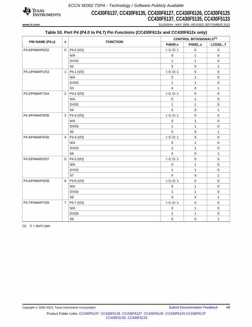
ECCN 5E002 TSPA - Technology / Software Publicly Available
CC430F6137, CC430F6135, CC430F6127, CC430F6126, CC430F6125CC430F5137, CC430F5135, CC430F5133
www.ti.com SLAS554H –MAY 2009–REVISED SEPTEMBER 2013
Table 53. Port P4 (P4.0 to P4.7) Pin Functions (CC430F613x and CC430F612x only)CONTROL BITS/SIGNALS (1)
PIN NAME (P4.x) x FUNCTIONP4DIR.x P4SEL.x LCDS2...7
P4.0/P4MAP0/S2 0 P4.0 (I/O) I: 0; O: 1 0 0N/A 0 1 0DVSS 1 1 0S2 X X 1
P4.1/P4MAP1/S3 1 P4.1 (I/O) I: 0; O: 1 0 0N/A 0 1 0DVSS 1 1 0S3 X X 1
P4.2/P4MAP7/S4 2 P4.2 (I/O) I: 0; O: 1 0 0N/A 0 1 0DVSS 1 1 0S4 X X 1
P4.3/P4MAP3/S5 3 P4.3 (I/O) I: 0; O: 1 0 0N/A 0 1 0DVSS 1 1 0S5 X X 1
P4.4/P4MAP4/S6 4 P4.4 (I/O) I: 0; O: 1 0 0N/A 0 1 0DVSS 1 1 0S6 X X 1
P4.5/P4MAP5/S7 5 P4.5 (I/O) I: 0; O: 1 0 0N/A 0 1 0DVSS 1 1 0S7 X X 1
P4.6/P4MAP6/S8 6 P4.6 (I/O) I: 0; O: 1 0 0N/A 0 1 0DVSS 1 1 0S8 X X 1
P4.7/P4MAP7/S9 7 P4.7 (I/O) I: 0; O: 1 0 0N/A 0 1 0DVSS 1 1 0S9 X X 1
(1) X = don't care
Copyright © 2009–2013, Texas Instruments Incorporated Submit Documentation Feedback 99
Product Folder Links: CC430F6137 CC430F6135 CC430F6127 CC430F6126 CC430F6125 CC430F5137CC430F5135 CC430F5133

P5.0/XIN
P5SEL.0
1
0P5DIR.0
P5IN.0
EN
Module X IN
1
0
Module X OUT
P5OUT.0
1
0DVSS
DVCC
P5REN.0
Pad Logic
1
P5DS.x
0: Low drive
1: High drive
D
Bus
Keeper
to XT1
ECCN 5E002 TSPA - Technology / Software Publicly Available
CC430F6137, CC430F6135, CC430F6127, CC430F6126, CC430F6125CC430F5137, CC430F5135, CC430F5133SLAS554H –MAY 2009–REVISED SEPTEMBER 2013 www.ti.com
Port P5, P5.0, Input/Output With Schmitt Trigger
100 Submit Documentation Feedback Copyright © 2009–2013, Texas Instruments Incorporated
Product Folder Links: CC430F6137 CC430F6135 CC430F6127 CC430F6126 CC430F6125 CC430F5137CC430F5135 CC430F5133

P5.1/XOUTP5SEL.0
XT1BYPASS
1
0P5DIR.1
P5IN.1
EN
Module X IN
1
0
Module X OUT
P5OUT.1
1
0DVSS
DVCC
P5REN.1
Pad Logic
1
P5DS.x
0: Low drive
1: High drive
D
Bus
Keeper
to XT1
ECCN 5E002 TSPA - Technology / Software Publicly Available
CC430F6137, CC430F6135, CC430F6127, CC430F6126, CC430F6125CC430F5137, CC430F5135, CC430F5133
www.ti.com SLAS554H –MAY 2009–REVISED SEPTEMBER 2013
Port P5, P5.1, Input/Output With Schmitt Trigger
Table 54. Port P5 (P5.0 and P5.1) Pin FunctionsCONTROL BITS/SIGNALS (1)
PIN NAME (P5.x) x FUNCTIONP5DIR.x P5SEL.0 P5SEL.1 XT1BYPASS
P5.0/XIN 0 P5.0 (I/O) I: 0; O: 1 0 X XXIN crystal mode (2) X 1 X 0XIN bypass mode (2) X 1 X 1
P5.1/XOUT 1 P5.1 (I/O) I: 0; O: 1 0 X XXOUT crystal mode (3) X 1 X 0P5.1 (I/O) (3) X 1 X 1
(1) X = don't care(2) Setting P5SEL.0 causes the general-purpose I/O to be disabled. Pending the setting of XT1BYPASS, P5.0 is configured for crystal
mode or bypass mode.(3) Setting P5SEL.0 causes the general-purpose I/O to be disabled in crystal mode. When using bypass mode, P5.1 can be used as
general-purpose I/O.
Copyright © 2009–2013, Texas Instruments Incorporated Submit Documentation Feedback 101
Product Folder Links: CC430F6137 CC430F6135 CC430F6127 CC430F6126 CC430F6125 CC430F5137CC430F5135 CC430F5133

P5.2/S0
P5.3/S1
P5.4/S23P5SEL.x
1
0P5DIR.x
P5IN.x
EN
Not Used
1
0
DVSS
P5OUT.x
1
0DVSS
DVCC
P5REN.x
Pad Logic
1
P5DS.x
0: Low drive
1: High drive
D
Bus
Keeper
S0(P5.2)/S1(P5.3)/S23(P5.4)
LCDS0(P5.2)/LCDS1(P5.3)/LCDS23(P5.4)
ECCN 5E002 TSPA - Technology / Software Publicly Available
CC430F6137, CC430F6135, CC430F6127, CC430F6126, CC430F6125CC430F5137, CC430F5135, CC430F5133SLAS554H –MAY 2009–REVISED SEPTEMBER 2013 www.ti.com
Port P5, P5.2 to P5.4, Input/Output With Schmitt Trigger (CC430F613x and CC430F612x only)
Table 55. Port P5 (P5.2 to P5.3) Pin Functions (CC430F613x and CC430F612x only)CONTROL BITS/SIGNALS (1)
PIN NAME (P5.x) x FUNCTIONP5DIR.x P5SEL.x LCDS0...1
P5.2/S0 2 P5.2 (I/O) I: 0; O: 1 0 0N/A 0 1 0DVSS 1 1 0S0 X X 1
P5.3/S1 3 P5.3 (I/O) I: 0; O: 1 0 0N/A 0 1 0DVSS 1 1 0S1 X X 1
(1) X = don't care
Table 56. Port P5 (P5.4) Pin Functions (CC430F613x and CC430F612x only)CONTROL BITS/SIGNALS (1)
PIN NAME (P5.x) x FUNCTIONP5DIR.x P5SEL.x LCDS23
P5.4/S23 4 P5.4 (I/O) I: 0; O: 1 0 0N/A 0 1 0DVSS 1 1 0S23 X X 1
(1) X = don't care
102 Submit Documentation Feedback Copyright © 2009–2013, Texas Instruments Incorporated
Product Folder Links: CC430F6137 CC430F6135 CC430F6127 CC430F6126 CC430F6125 CC430F5137CC430F5135 CC430F5133

P5.5/COM3/S24
P5.6/COM2/S25
P5.7/COM1/S26P5SEL.x
P5DIR.x
P5IN.x
P5OUT.x
1
0DVSS
DVCC
P5REN.x
Pad Logic
1
P5DS.x
0: Low drive
1: High drive
Bus
Keeper
COM3(P5.5)/COM2(P5.6)/COM1(P5.7)
S24(P5.5)/S25(P5.6)/S26(P5.7)
LCDS24(P5.5)/LCDS25(P5.6)/LCDS26(P5.7)
ECCN 5E002 TSPA - Technology / Software Publicly Available
CC430F6137, CC430F6135, CC430F6127, CC430F6126, CC430F6125CC430F5137, CC430F5135, CC430F5133
www.ti.com SLAS554H –MAY 2009–REVISED SEPTEMBER 2013
Port P5, P5.5 to P5.7, Input/Output With Schmitt Trigger (CC430F613x and CC430F612x only)
Table 57. Port P5 (P5.5 to P5.7) Pin Functions (CC430F613x and CC430F612x only)CONTROL BITS/SIGNALS (1)
PIN NAME (P5.x) x FUNCTIONP5DIR.x P5SEL.x LCDS24...26
P5.5/COM3/S24 5 P5.5 (I/O) I: 0; O: 1 0 0COM3 (2) X 1 XS24 (2) X 0 1
P5.6/COM2/S25 6 P5.6 (I/O) I: 0; O: 1 0 0COM2 (2) X 1 XS25 (2) X 0 1
P5.7/COM1/S26 7 P5.7 (I/O) I: 0; O: 1 0 0COM1 (2) X 1 XS26 (2) X 0 1
(1) X = don't care(2) Setting P5SEL.x bit disables the output driver as well as the input Schmitt trigger.
Copyright © 2009–2013, Texas Instruments Incorporated Submit Documentation Feedback 103
Product Folder Links: CC430F6137 CC430F6135 CC430F6127 CC430F6126 CC430F6125 CC430F5137CC430F5135 CC430F5133

PJ.1/TDI/TCLK
PJ.2/TMS
PJ.3/TCKFrom JTAG
1
0PJDIR.x
PJIN.x
EN
1
0
From JTAG
PJOUT.x
1
0DVSS
DVCC
PJREN.xPad Logic
1
PJDS.x
0: Low drive
1: High drive
D
DVSS
To JTAG
PJ.0/TDO
From JTAG
1
0PJDIR.0
PJIN.0
1
0
From JTAG
PJOUT.0
1
0DVSS
DVCC
PJREN.0Pad Logic
1
PJDS.0
0: Low drive
1: High drive
DVCC
ECCN 5E002 TSPA - Technology / Software Publicly Available
CC430F6137, CC430F6135, CC430F6127, CC430F6126, CC430F6125CC430F5137, CC430F5135, CC430F5133SLAS554H –MAY 2009–REVISED SEPTEMBER 2013 www.ti.com
Port J, J.0 JTAG pin TDO, Input/Output With Schmitt Trigger or Output
Port J, J.1 to J.3 JTAG pins TMS, TCK, TDI/TCLK, Input/Output With Schmitt Trigger or Output
104 Submit Documentation Feedback Copyright © 2009–2013, Texas Instruments Incorporated
Product Folder Links: CC430F6137 CC430F6135 CC430F6127 CC430F6126 CC430F6125 CC430F5137CC430F5135 CC430F5133

ECCN 5E002 TSPA - Technology / Software Publicly Available
CC430F6137, CC430F6135, CC430F6127, CC430F6126, CC430F6125CC430F5137, CC430F5135, CC430F5133
www.ti.com SLAS554H –MAY 2009–REVISED SEPTEMBER 2013
Table 58. Port PJ (PJ.0 to PJ.3) Pin FunctionsCONTROL BITS/
SIGNALS (1)PIN NAME (PJ.x) x FUNCTIONPJDIR.x
PJ.0/TDO 0 PJ.0 (I/O) (2) I: 0; O: 1TDO (3) X
PJ.1/TDI/TCLK 1 PJ.1 (I/O) (2) I: 0; O: 1TDI/TCLK (3) (4) X
PJ.2/TMS 2 PJ.2 (I/O) (2) I: 0; O: 1TMS (3) (4) X
PJ.3/TCK 3 PJ.3 (I/O) (2) I: 0; O: 1TCK (3) (4) X
(1) X = don't care(2) Default condition(3) The pin direction is controlled by the JTAG module.(4) In JTAG mode, pullups are activated automatically on TMS, TCK, and TDI/TCLK. PJREN.x are do not care.
Copyright © 2009–2013, Texas Instruments Incorporated Submit Documentation Feedback 105
Product Folder Links: CC430F6137 CC430F6135 CC430F6127 CC430F6126 CC430F6125 CC430F5137CC430F5135 CC430F5133

ECCN 5E002 TSPA - Technology / Software Publicly Available
CC430F6137, CC430F6135, CC430F6127, CC430F6126, CC430F6125CC430F5137, CC430F5135, CC430F5133SLAS554H –MAY 2009–REVISED SEPTEMBER 2013 www.ti.com
Device Descriptor StructuresTable 59 lists the content of the device descriptor tag-length-value (TLV) structure for CC430F613x andCC430F513x device types.
Table 60 lists the content of the device descriptor tag-length-value (TLV) structure for CC430F612x device types.
Table 59. Device Descriptor Table (CC430F613x and CC430F513x)'F6137 'F6135 'F5137 'F5135 'F5133SizeDescription Address bytes Value Value Value Value Value
Info Block Info length 01A00h 1 06h 06h 06h 06h 06hCRC length 01A01h 1 06h 06h 06h 06h 06hCRC value 01A02h 2 per unit per unit per unit per unit per unitDevice ID 01A04h 1 61h 61h 51h 51h 51hDevice ID 01A05h 1 37h 35h 37h 35h 33h
Hardware revision 01A06h 1 per unit per unit per unit per unit per unitFirmware revision 01A07h 1 per unit per unit per unit per unit per unit
Die Record Die Record Tag 01A08h 1 08h 08h 08h 08h 08hDie Record length 01A09h 1 0Ah 0Ah 0Ah 0Ah 0Ah
Lot/Wafer ID 01A0Ah 4 per unit per unit per unit per unit per unitDie X position 01A0Eh 2 per unit per unit per unit per unit per unitDie Y position 01A10h 2 per unit per unit per unit per unit per unitTest results 01A12h 2 per unit per unit per unit per unit per unit
ADC12 ADC12 Calibration 01A14h 1 11h 11h 11h 11h 11hCalibration TagADC12 Calibration 01A15h 1 10h 10h 10h 10h 10hlengthADC Gain Factor 01A16h 2 per unit per unit per unit per unit per unit
ADC Offset 01A18h 2 per unit per unit per unit per unit per unitADC 1.5VReference 01A1Ah 2 per unit per unit per unit per unit per unitTemp. Sensor
30°CADC 1.5VReference 01A1Ch 2 per unit per unit per unit per unit per unitTemp. Sensor
85°CADC 2.0VReference 01A1Eh 2 per unit per unit per unit per unit per unitTemp. Sensor
30°CADC 2.0VReference 01A20h 2 per unit per unit per unit per unit per unitTemp. Sensor
85°CADC 2.5VReference 01A22h 2 per unit per unit per unit per unit per unitTemp. Sensor
30°CADC 2.5VReference 01A24h 2 per unit per unit per unit per unit per unitTemp. Sensor
85°CREF REF Calibration 01A26h 1 12h 12h 12h 12h 12hCalibration Tag
REF Calibration 01A27h 1 06h 06h 06h 06h 06hlength
106 Submit Documentation Feedback Copyright © 2009–2013, Texas Instruments Incorporated
Product Folder Links: CC430F6137 CC430F6135 CC430F6127 CC430F6126 CC430F6125 CC430F5137CC430F5135 CC430F5133

ECCN 5E002 TSPA - Technology / Software Publicly Available
CC430F6137, CC430F6135, CC430F6127, CC430F6126, CC430F6125CC430F5137, CC430F5135, CC430F5133
www.ti.com SLAS554H –MAY 2009–REVISED SEPTEMBER 2013
Table 59. Device Descriptor Table (CC430F613x and CC430F513x) (continued)'F6137 'F6135 'F5137 'F5135 'F5133SizeDescription Address bytes Value Value Value Value Value
1.5V Reference 01A28h 2 per unit per unit per unit per unit per unitFactor2.0V Reference 01A2Ah 2 per unit per unit per unit per unit per unitFactor2.5V Reference 01A2Ch 2 per unit per unit per unit per unit per unitFactor
Peripheral Peripheral 01A2Eh 1 02h 02h 02h 02h 02hDescriptor Descriptor Tag(PD) Peripheral 01A2Fh 1 57h 57h 55h 55h 55hDescriptor Length
Peripheral PD01A30h ... ... ... ... ...Descriptors Length
Table 60. Device Descriptor Table (CC430F612x)'F6127 'F6126 'F6125SizeDescription Address bytes Value Value Value
Info Block Info length 01A00h 1 06h 06h 06hCRC length 01A01h 1 06h 06h 06hCRC value 01A02h 2 per unit per unit per unitDevice ID 01A04h 1 61h 61h 61hDevice ID 01A05h 1 27h 26h 25h
Hardware revision 01A06h 1 per unit per unit per unitFirmware revision 01A07h 1 per unit per unit per unit
Die Record Die Record Tag 01A08h 1 08h 08h 08hDie Record length 01A09h 1 0Ah 0Ah 0Ah
Lot/Wafer ID 01A0Ah 4 per unit per unit per unitDie X position 01A0Eh 2 per unit per unit per unitDie Y position 01A10h 2 per unit per unit per unitTest results 01A12h 2 per unit per unit per unit
Empty Descriptor Empty Tag 01A14h 1 05h 05h 05hEmpty Tag Length 01A15h 1 10h 10h 10h
01A16h 16 undefined undefined undefinedREF Calibration REF Calibration Tag 01A26h 1 12h 12h 12h
REF Calibration length 01A27h 1 06h 06h 06h1.5V Reference Factor 01A28h 2 per unit per unit per unit2.0V Reference Factor 01A2Ah 2 per unit per unit per unit2.5V Reference Factor 01A2Ch 2 per unit per unit per unit
Peripheral Peripheral Descriptor Tag 01A2Eh 1 02h 02h 02hDescriptor (PD) Peripheral Descriptor 01A2Fh 1 55h 55h 55hLength
Peripheral Descriptors 01A30h PD Length ... ... ...
Copyright © 2009–2013, Texas Instruments Incorporated Submit Documentation Feedback 107
Product Folder Links: CC430F6137 CC430F6135 CC430F6127 CC430F6126 CC430F6125 CC430F5137CC430F5135 CC430F5133

ECCN 5E002 TSPA - Technology / Software Publicly Available
CC430F6137, CC430F6135, CC430F6127, CC430F6126, CC430F6125CC430F5137, CC430F5135, CC430F5133SLAS554H –MAY 2009–REVISED SEPTEMBER 2013 www.ti.com
REVISION HISTORY
REVISION DESCRIPTIONSLAS554 Product Preview data sheet release
SLAS554A Product Preview data sheet updated with electrical parametersSLAS554B Production Data release data sheet for CC430F51xx devices. CC430F61xx devices are Product Preview.SLAS554C Production Data release data sheet for CC430F61xx devices.
Added correct termination of LCDCAP/R33 if not used.SLAS554D Corrected unit in Frequency Synthesizer Characteristics from "ms" to "µs".
Removed RFRXIFG (14) and RFTXIFG (15) from DMA Trigger Assignments tableCorrected USCI control register location in Peripheral File Map.SLAS554EChanged Tstg maximum limit from 105°C to 150°C in Absolute Maximum Ratings.Replaced values for "Hardware revision" and "Firmware revision" in Device Descriptor Tables with "per unit".
Table 3, Corrected USCI signal names for pins 5 and 6 (descriptions unchanged).12-Bit ADC, Linearity Parameters Using an External Reference Voltage or AVCC as Reference Voltage, ADC12 linearity
SLAS554F parameter test conditions revised.12-Bit ADC, Linearity Parameters Using the Internal Reference Voltage, linearity parameters with internal referenceadded.
Table 11, Changed SYSRSTIV interrupt event at 1Ch to Reserved.Recommended Operating Conditions, Added test conditions for typical characteristics.
SLAS554G Recommended Operating Conditions, Added note regarding relationship between SVS and MIN VCC.DCO Frequency, Added note (1).Flash Memory, Changed IERASE and IMERASE values.
Applications, Added section.SLAS554H Recommended Operating Conditions, Added note about CVCORE tolerance.
Peripheral File Map, Removed CRCRESR and CRCDIRB registers (do not apply).
108 Submit Documentation Feedback Copyright © 2009–2013, Texas Instruments Incorporated
Product Folder Links: CC430F6137 CC430F6135 CC430F6127 CC430F6126 CC430F6125 CC430F5137CC430F5135 CC430F5133

PACKAGE OPTION ADDENDUM
www.ti.com 30-Oct-2015
Addendum-Page 1
PACKAGING INFORMATION
Orderable Device Status(1)
Package Type PackageDrawing
Pins PackageQty
Eco Plan(2)
Lead/Ball Finish(6)
MSL Peak Temp(3)
Op Temp (°C) Device Marking(4/5)
Samples
CC430F5133IRGZ ACTIVE VQFN RGZ 48 52 Green (RoHS& no Sb/Br)
CU NIPDAU Level-3-260C-168 HR -40 to 85 CC430F5133
CC430F5133IRGZR ACTIVE VQFN RGZ 48 2500 Green (RoHS& no Sb/Br)
CU NIPDAU Level-3-260C-168 HR -40 to 85 CC430F5133
CC430F5133IRGZT ACTIVE VQFN RGZ 48 250 Green (RoHS& no Sb/Br)
CU NIPDAU Level-3-260C-168 HR -40 to 85 CC430F5133
CC430F5135IRGZ ACTIVE VQFN RGZ 48 52 Green (RoHS& no Sb/Br)
CU NIPDAU Level-3-260C-168 HR -40 to 85 CC430F5135
CC430F5135IRGZR ACTIVE VQFN RGZ 48 2500 Green (RoHS& no Sb/Br)
CU NIPDAU Level-3-260C-168 HR -40 to 85 CC430F5135
CC430F5135IRGZT ACTIVE VQFN RGZ 48 250 Green (RoHS& no Sb/Br)
CU NIPDAU Level-3-260C-168 HR -40 to 85 CC430F5135
CC430F5137IRGZ ACTIVE VQFN RGZ 48 52 Green (RoHS& no Sb/Br)
CU NIPDAU Level-3-260C-168 HR -40 to 85 CC430F5137
CC430F5137IRGZR ACTIVE VQFN RGZ 48 2500 Green (RoHS& no Sb/Br)
CU NIPDAU Level-3-260C-168 HR -40 to 85 CC430F5137
CC430F5137IRGZT ACTIVE VQFN RGZ 48 250 Green (RoHS& no Sb/Br)
CU NIPDAU Level-3-260C-168 HR -40 to 85 CC430F5137
CC430F6125IRGCR ACTIVE VQFN RGC 64 2000 Green (RoHS& no Sb/Br)
CU NIPDAU Level-3-260C-168 HR -40 to 85 CC430F6125
CC430F6126IRGCR ACTIVE VQFN RGC 64 2000 Green (RoHS& no Sb/Br)
CU NIPDAU Level-3-260C-168 HR -40 to 85 CC430F6126
CC430F6126IRGCT ACTIVE VQFN RGC 64 250 Green (RoHS& no Sb/Br)
CU NIPDAU Level-3-260C-168 HR -40 to 85 CC430F6126
CC430F6127IRGCR ACTIVE VQFN RGC 64 2000 Green (RoHS& no Sb/Br)
CU NIPDAU Level-3-260C-168 HR -40 to 85 CC430F6127
CC430F6127IRGCT ACTIVE VQFN RGC 64 250 Green (RoHS& no Sb/Br)
CU NIPDAU Level-3-260C-168 HR -40 to 85 CC430F6127
CC430F6135IRGCR ACTIVE VQFN RGC 64 2000 Green (RoHS& no Sb/Br)
CU NIPDAU Level-3-260C-168 HR -40 to 85 CC430F6135
CC430F6137IRGCR ACTIVE VQFN RGC 64 2000 Green (RoHS& no Sb/Br)
CU NIPDAU Level-3-260C-168 HR -40 to 85 CC430F6137
CC430F6137IRGCT ACTIVE VQFN RGC 64 250 Green (RoHS& no Sb/Br)
CU NIPDAU Level-3-260C-168 HR -40 to 85 CC430F6137

PACKAGE OPTION ADDENDUM
www.ti.com 30-Oct-2015
Addendum-Page 2
(1) The marketing status values are defined as follows:ACTIVE: Product device recommended for new designs.LIFEBUY: TI has announced that the device will be discontinued, and a lifetime-buy period is in effect.NRND: Not recommended for new designs. Device is in production to support existing customers, but TI does not recommend using this part in a new design.PREVIEW: Device has been announced but is not in production. Samples may or may not be available.OBSOLETE: TI has discontinued the production of the device.
(2) Eco Plan - The planned eco-friendly classification: Pb-Free (RoHS), Pb-Free (RoHS Exempt), or Green (RoHS & no Sb/Br) - please check http://www.ti.com/productcontent for the latest availabilityinformation and additional product content details.TBD: The Pb-Free/Green conversion plan has not been defined.Pb-Free (RoHS): TI's terms "Lead-Free" or "Pb-Free" mean semiconductor products that are compatible with the current RoHS requirements for all 6 substances, including the requirement thatlead not exceed 0.1% by weight in homogeneous materials. Where designed to be soldered at high temperatures, TI Pb-Free products are suitable for use in specified lead-free processes.Pb-Free (RoHS Exempt): This component has a RoHS exemption for either 1) lead-based flip-chip solder bumps used between the die and package, or 2) lead-based die adhesive used betweenthe die and leadframe. The component is otherwise considered Pb-Free (RoHS compatible) as defined above.Green (RoHS & no Sb/Br): TI defines "Green" to mean Pb-Free (RoHS compatible), and free of Bromine (Br) and Antimony (Sb) based flame retardants (Br or Sb do not exceed 0.1% by weightin homogeneous material)
(3) MSL, Peak Temp. - The Moisture Sensitivity Level rating according to the JEDEC industry standard classifications, and peak solder temperature.
(4) There may be additional marking, which relates to the logo, the lot trace code information, or the environmental category on the device.
(5) Multiple Device Markings will be inside parentheses. Only one Device Marking contained in parentheses and separated by a "~" will appear on a device. If a line is indented then it is a continuationof the previous line and the two combined represent the entire Device Marking for that device.
(6) Lead/Ball Finish - Orderable Devices may have multiple material finish options. Finish options are separated by a vertical ruled line. Lead/Ball Finish values may wrap to two lines if the finishvalue exceeds the maximum column width.
Important Information and Disclaimer:The information provided on this page represents TI's knowledge and belief as of the date that it is provided. TI bases its knowledge and belief on informationprovided by third parties, and makes no representation or warranty as to the accuracy of such information. Efforts are underway to better integrate information from third parties. TI has taken andcontinues to take reasonable steps to provide representative and accurate information but may not have conducted destructive testing or chemical analysis on incoming materials and chemicals.TI and TI suppliers consider certain information to be proprietary, and thus CAS numbers and other limited information may not be available for release.
In no event shall TI's liability arising out of such information exceed the total purchase price of the TI part(s) at issue in this document sold by TI to Customer on an annual basis.

TAPE AND REEL INFORMATION
*All dimensions are nominal
Device PackageType
PackageDrawing
Pins SPQ ReelDiameter
(mm)
ReelWidth
W1 (mm)
A0(mm)
B0(mm)
K0(mm)
P1(mm)
W(mm)
Pin1Quadrant
CC430F5135IRGZR VQFN RGZ 48 2500 330.0 16.4 7.3 7.3 1.5 12.0 16.0 Q2
CC430F5135IRGZT VQFN RGZ 48 250 180.0 16.4 7.3 7.3 1.5 12.0 16.0 Q2
CC430F5137IRGZR VQFN RGZ 48 2500 330.0 16.4 7.3 7.3 1.5 12.0 16.0 Q2
CC430F5137IRGZT VQFN RGZ 48 250 180.0 16.4 7.3 7.3 1.5 12.0 16.0 Q2
CC430F6125IRGCR VQFN RGC 64 2000 330.0 16.4 9.3 9.3 1.5 12.0 16.0 Q2
CC430F6126IRGCR VQFN RGC 64 2000 330.0 16.4 9.3 9.3 1.5 12.0 16.0 Q2
CC430F6126IRGCT VQFN RGC 64 250 180.0 16.4 9.3 9.3 1.5 12.0 16.0 Q2
CC430F6127IRGCR VQFN RGC 64 2000 330.0 16.4 9.3 9.3 1.5 12.0 16.0 Q2
CC430F6127IRGCT VQFN RGC 64 250 180.0 16.4 9.3 9.3 1.5 12.0 16.0 Q2
CC430F6135IRGCR VQFN RGC 64 2000 330.0 16.4 9.3 9.3 1.5 12.0 16.0 Q2
CC430F6137IRGCR VQFN RGC 64 2000 330.0 16.4 9.3 9.3 1.5 12.0 16.0 Q2
CC430F6137IRGCT VQFN RGC 64 250 180.0 16.4 9.3 9.3 1.5 12.0 16.0 Q2
PACKAGE MATERIALS INFORMATION
www.ti.com 26-Jun-2015
Pack Materials-Page 1

*All dimensions are nominal
Device Package Type Package Drawing Pins SPQ Length (mm) Width (mm) Height (mm)
CC430F5135IRGZR VQFN RGZ 48 2500 336.6 336.6 28.6
CC430F5135IRGZT VQFN RGZ 48 250 213.0 191.0 55.0
CC430F5137IRGZR VQFN RGZ 48 2500 336.6 336.6 28.6
CC430F5137IRGZT VQFN RGZ 48 250 213.0 191.0 55.0
CC430F6125IRGCR VQFN RGC 64 2000 336.6 336.6 28.6
CC430F6126IRGCR VQFN RGC 64 2000 336.6 336.6 28.6
CC430F6126IRGCT VQFN RGC 64 250 213.0 191.0 55.0
CC430F6127IRGCR VQFN RGC 64 2000 336.6 336.6 28.6
CC430F6127IRGCT VQFN RGC 64 250 213.0 191.0 55.0
CC430F6135IRGCR VQFN RGC 64 2000 336.6 336.6 28.6
CC430F6137IRGCR VQFN RGC 64 2000 336.6 336.6 28.6
CC430F6137IRGCT VQFN RGC 64 250 213.0 191.0 55.0
PACKAGE MATERIALS INFORMATION
www.ti.com 26-Jun-2015
Pack Materials-Page 2


IMPORTANT NOTICE
Texas Instruments Incorporated and its subsidiaries (TI) reserve the right to make corrections, enhancements, improvements and otherchanges to its semiconductor products and services per JESD46, latest issue, and to discontinue any product or service per JESD48, latestissue. Buyers should obtain the latest relevant information before placing orders and should verify that such information is current andcomplete. All semiconductor products (also referred to herein as “components”) are sold subject to TI’s terms and conditions of salesupplied at the time of order acknowledgment.TI warrants performance of its components to the specifications applicable at the time of sale, in accordance with the warranty in TI’s termsand conditions of sale of semiconductor products. Testing and other quality control techniques are used to the extent TI deems necessaryto support this warranty. Except where mandated by applicable law, testing of all parameters of each component is not necessarilyperformed.TI assumes no liability for applications assistance or the design of Buyers’ products. Buyers are responsible for their products andapplications using TI components. To minimize the risks associated with Buyers’ products and applications, Buyers should provideadequate design and operating safeguards.TI does not warrant or represent that any license, either express or implied, is granted under any patent right, copyright, mask work right, orother intellectual property right relating to any combination, machine, or process in which TI components or services are used. Informationpublished by TI regarding third-party products or services does not constitute a license to use such products or services or a warranty orendorsement thereof. Use of such information may require a license from a third party under the patents or other intellectual property of thethird party, or a license from TI under the patents or other intellectual property of TI.Reproduction of significant portions of TI information in TI data books or data sheets is permissible only if reproduction is without alterationand is accompanied by all associated warranties, conditions, limitations, and notices. TI is not responsible or liable for such altereddocumentation. Information of third parties may be subject to additional restrictions.Resale of TI components or services with statements different from or beyond the parameters stated by TI for that component or servicevoids all express and any implied warranties for the associated TI component or service and is an unfair and deceptive business practice.TI is not responsible or liable for any such statements.Buyer acknowledges and agrees that it is solely responsible for compliance with all legal, regulatory and safety-related requirementsconcerning its products, and any use of TI components in its applications, notwithstanding any applications-related information or supportthat may be provided by TI. Buyer represents and agrees that it has all the necessary expertise to create and implement safeguards whichanticipate dangerous consequences of failures, monitor failures and their consequences, lessen the likelihood of failures that might causeharm and take appropriate remedial actions. Buyer will fully indemnify TI and its representatives against any damages arising out of the useof any TI components in safety-critical applications.In some cases, TI components may be promoted specifically to facilitate safety-related applications. With such components, TI’s goal is tohelp enable customers to design and create their own end-product solutions that meet applicable functional safety standards andrequirements. Nonetheless, such components are subject to these terms.No TI components are authorized for use in FDA Class III (or similar life-critical medical equipment) unless authorized officers of the partieshave executed a special agreement specifically governing such use.Only those TI components which TI has specifically designated as military grade or “enhanced plastic” are designed and intended for use inmilitary/aerospace applications or environments. Buyer acknowledges and agrees that any military or aerospace use of TI componentswhich have not been so designated is solely at the Buyer's risk, and that Buyer is solely responsible for compliance with all legal andregulatory requirements in connection with such use.TI has specifically designated certain components as meeting ISO/TS16949 requirements, mainly for automotive use. In any case of use ofnon-designated products, TI will not be responsible for any failure to meet ISO/TS16949.
Products ApplicationsAudio www.ti.com/audio Automotive and Transportation www.ti.com/automotiveAmplifiers amplifier.ti.com Communications and Telecom www.ti.com/communicationsData Converters dataconverter.ti.com Computers and Peripherals www.ti.com/computersDLP® Products www.dlp.com Consumer Electronics www.ti.com/consumer-appsDSP dsp.ti.com Energy and Lighting www.ti.com/energyClocks and Timers www.ti.com/clocks Industrial www.ti.com/industrialInterface interface.ti.com Medical www.ti.com/medicalLogic logic.ti.com Security www.ti.com/securityPower Mgmt power.ti.com Space, Avionics and Defense www.ti.com/space-avionics-defenseMicrocontrollers microcontroller.ti.com Video and Imaging www.ti.com/videoRFID www.ti-rfid.comOMAP Applications Processors www.ti.com/omap TI E2E Community e2e.ti.comWireless Connectivity www.ti.com/wirelessconnectivity
Mailing Address: Texas Instruments, Post Office Box 655303, Dallas, Texas 75265Copyright © 2015, Texas Instruments Incorporated


![Vortrag zur Seminarphase der PG „Solar Doorplate“ MSP430 ... · MSP430 – Wichtigste Grundlagen von David Tondorf. 2 ... MSP430 microcontroller basics. Oxford: Newnes [4] MSP430](https://img.dokumen.tips/doc/110x75/5b6f6a9b7f8b9af12d8c481e/vortrag-zur-seminarphase-der-pg-solar-doorplate-msp430-msp430-.jpg)