Embed Size (px)
Citation preview

S E M I C O N D U C T O R
3-1
November 1996
CA5130, CA5130A15MHz, BiMOS Microprocessor Operational
Amplifiers with MOSFET Input/CMOS Output
CAUTION: These devices are sensitive to electrostatic discharge. Users should follow proper IC Handling Procedures.
Copyright © Harris Corporation 1996File Number 1923.3
Features• MOSFET Input Stage
- Very High Z l . . . . . . . . . . . . 1.5TΩ (1.5 x 10¹²Ω) (Typ)- Very Low l l . . . . . . . . . . . 5pA (Typ) at 15V Operation
2pA (Typ) at 5V Operation
• Ideal for Single Supply Applications
• Common Mode Input Voltage Range IncludesNegative Supply Rail; Input Terminals Can BeSwung 0.5V Below Negative Supply Rail
• CMOS Output Stage Permits Signal Swing to Either (orBoth) Supply Rails
• CA5130A, CA5130 Have Full Military Temperature RangeGuaranteed Specifications for V+ = 5V
• CA5130A, CA5130 Are Guaranteed to Operate Down toV+ = 4.5V for A OL
• CA5130A, CA5130 Are Guaranteed to Operate at ±7.5VCA3130A, CA3130 Specifications
Applications• Ground Referenced Single Supply Amplifiers• Fast Sample-Hold Amplifiers• Long Duration Timers/Monostables• High Input lmpedance Comparators (Ideal Interface
with Digital CMOS)• High lnput Impedance Wideband Amplifiers• Voltage Followers (e.g., Follower for Single-Supply
D/A Converter)• Voltage Regulators (Permits Control of Output Voltage
Down to 0V)• Peak Detectors• Single Supply Full Wave Precision Rectifiers• Photo Diode Sensor Amplifiers• 5V Logic Systems• Microprocessor Interface
DescriptionCA5130A and CA5130 are integrated circuit operationalamplifiers that combine the advantage of both CMOS andbipolar transistors on a monolithic chip. They are designedand guaranteed to operate in microprocessors or logicsystems that use +5V supplies.
Gate protected P-Channel MOSFET (PMOS) transistors areused in the input circuit to provide very high inputimpedance, very low input current, and exceptional speedperformance. The use of PMOS field effect transistors in theinput stage results in common mode input voltage capabilitydown to 0.5V below the negative supply terminal, animportant attribute in single supply applications.
A complementary symmetry MOS (CMOS) transistor-pair,capable of swinging the output voltage to within 10mV ofeither supply voltage terminal (at very high values of loadimpedance), is employed as the output circuit.
The CA5130 Series circuits operate at supply voltages rangingfrom 4V to 16V, or ±2V to ±8V when using split supplies. Theycan be phase compensated with a single external capacitor,and have terminals for adjustment of offset voltage forapplications requiring offset null capability. Terminal provisionsare also made to permit strobing of the output stage.
The CA5130A, CA5130 have guaranteed specifications for5V operation over the full military temperature range of-55oC to 125oC.
Pinouts
Ordering InformationPART NUMBER
(BRAND)TEMP.
RANGE (oC) PACKAGEPKG.NO.
CA5130AE -55 to 125 8 Ld PDIP E8.3
CA5130AM(5130A)
-55 to 125 8 Ld SOIC M8.15
CA5130AT -55 to 125 8 Pin Metal Can T8.C
CA5130E -55 to 125 8 Ld PDIP E8.3
CA5130M(5130)
-55 to 125 8 Ld SOIC M8.15
CA5130 (PDIP, SOIC)TOP VIEW
CA5130 (METAL CAN)TOP VIEW
1
2
3
4
8
7
6
5
V+
OFFSET NULL
INV. INPUT
V-
NON-INV. INPUT
STROBE
OUTPUT
OFFSET NULL
+ OUTPUT
OFFSET NULL4
6
1
3
7
5
8
+
V+
V- AND CASE
NON-INV. INPUT
INV. INPUT
TAB
OFFSET NULL
2
STROBEPHASE
COMPENSATION
NOT RECOMMENDED FOR NEW DESIGNS

3-2
Absolute Maximum Ratings Thermal InformationSupply Voltage (V+ to V-) . . . . . . . . . . . . . . . . . . . . . . . . . . . . . . 16VDC Input Voltage . . . . . . . . . . . . . . . . . . . . . . (V+ +8V) to (V- -0.5V)Differential Input Voltage. . . . . . . . . . . . . . . . . . . . . . . . . . . . . . . . 8VInput Terminal Current . . . . . . . . . . . . . . . . . . . . . . . . . . . . . . . . 1mAOutput Short-Circuit Duration (Note 1) . . . . . . . . . . . . . . . . Indefinite
Operating ConditionsTemperature Range . . . . . . . . . . . . . . . . . . . . . . . . . -55oC to 125oC
Thermal Resistance (Typical, Note 2) θJA (oC/W) θJC (oC/W)PDIP Package . . . . . . . . . . . . . . . . . . . 125 N/ASOIC Package . . . . . . . . . . . . . . . . . . . 165 N/AMetal Can Package . . . . . . . . . . . . . . . 165 80
Maximum Junction Temperature (Can) . . . . . . . . . . . . . . . . . . 175oCMaximum Junction Temperature (Plastic Package) . . . . . . . 150oCMaximum Storage Temperature Range . . . . . . . . . -65oC to 150oCMaximum Lead Temperature (Soldering 10s) . . . . . . . . . . . . 300oC
(SOIC - Lead Tips Only)
CAUTION: Stresses above those listed in “Absolute Maximum Ratings” may cause permanent damage to the device. This is a stress only rating and operationof the device at these or any other conditions above those indicated in the operational sections of this specification is not implied.
NOTES:
1. Short circuit may be applied to ground or to either supply.
2. θJA is measured with the component mounted on an evaluation PC board in free air.
Electrical Specifications TA = 25oC, V+ = 5V, V- = 0V, Unless Otherwise Specified
PARAMETER SYMBOLTEST
CONDITIONS
CA5130 CA5130A
UNITSMIN TYP MAX MIN TYP MAX
Input Offset Voltage VIO VO = 2.5V - 2 10 - 1.5 4 mV
Input Offset Current IIO VO = 2.5V - 0.1 10 - 0.1 5 pA
Input Current II VO = 2.5V - 2 15 - 2 10 pA
Common Mode Rejection Ratio CMRR VCM = 0V to 1V 70 85 - 75 87 - dB
VCM = 0V to 2.5V 60 69 - 60 69 - dB
Input Common Mode VoltageRange
VICR+ 2.5 2.8 - 2.5 2.8 - V
VICR- - -0.5 0 - -0.5 0 V
Power Supply Rejection Ratio PSRR ∆+ = 1V; ∆- = 1V 55 73 - 60 75 - dB
Large Signal Voltage Gain(Note 3)
AOL VO = 0.1V to 4.1VRL = ∞
95 105 - 100 105 - dB
VO = 0.1V to 3.6VRL = 10kΩ
85 95 - 90 97 - dB
Source Current ISOURCE VO = 0V 1.0 2.6 4.0 1.0 3.1 4.0 mA
Sink Current ISINK VO = 5V 1.0 1.7 4.0 1.0 1.4 4.0 mA
Output VoltageVOUTVOM+ RL = ∞ 4.99 5 - 4.99 5 - V
VOM- - 0 0.01 - 0 0.01 V
VOM+ RL = 10kΩ 4.4 4.7 - 4.4 4.7 - V
VOM- - 0 0.01 - 0 0.01 V
VOM+ RL = 2kΩ 2.5 3.5 - 2.5 3.5 - V
VOM- - 0 0.01 - 0 0.01 V
Supply Current ISUPPLY VO = 0V - 50 100 - 50 100 µA
VO = 2.5V - 260 400 - 260 400 µA
NOTE:
3. For V+ = 4.5V and V- = GND; VOUT = 0.5V to 3.2V at RL = 10kΩ.
Electrical Specifications TA = -55oC to 125oC, V+ = 5V, V- = 0V, Unless Otherwise Specified
PARAMETER SYMBOLTEST
CONDITIONS
CA5130 CA5130A
UNITSMIN TYP MAX MIN TYP MAX
Input Offset Voltage VIO VO = 2.5V - 3 15 - 2 10 mV
Input Offset Current IIO VO = 2.5V - 0.1 10 - 0.1 5 nA
Input Current II VO = 2.5V - 2 15 - 2 10 nA
Common Mode Rejection Ratio CMRR VCM = 0V to 1V 60 80 - 60 80 - dB
VCM = 0V to 2.5V 50 80 - 55 80 - dB
CA5130, CA5130A

3-3
Input Common Mode VoltageRange
VICR+ 2.5 2.8 - 2.5 2.8 - V
VICR- - -0.5 0 - -0.5 0 V
Power Supply Rejection Ratio PSRR ∆+ = 1V; ∆- = 1V 40 66 - 45 70 - dB
Large Signal Voltage Gain(Note 4)
AOL VO = 0.1V to 4.1VRL = ∞
90 98 - 94 98 - dB
VO = 0.1V to 3.6VRL = 10kΩ
75 85 - 80 88 - dB
Source Current ISOURCE VO = 0V 0.6 - 5.0 0.6 2.2 5.0 mA
Sink Current ISINK VO = 5V 0.6 - 5.0 0.6 1.15 5.0 mA
Output VoltageVOUTVOM+ RL = ∞ 4.99 5 - 4.99 5 - V
VOM- - 0 0.01 - 0 0.01 V
VOM+ RL = 10kΩ 4.0 4.6 - 4.0 4.6 - V
VOM- - 0 0.01 - 0 0.01 V
VOM+ RL = 2kΩ 2.0 3.0 - 2.0 3.0 - V
VOM- - 0 0.01 - 0 0.01 V
Supply Current ISUPPLY VO = 0V - 80 220 - 80 220 µA
VO = 2.5V - 300 500 - 300 500 µA
NOTE:
4. For V+ = 4.5V and V- = GND; VOUT = 0.5V to 3.2V at RL = 10kΩ.
Electrical Specifications TA = 25oC, V+ = 15V, V- = 0V, Unless Otherwise Specified
PARAMETER SYMBOLTEST
CONDITIONS
CA5130 CA5130A
UNITSMIN TYP MAX MIN TYP MAX
Input Offset Voltage VIO V± = ±7.5V - 8 15 - 2 5 mV
Input Offset Current IIO V± = ±7.5V - 0.5 30 - 0.5 20 pA
Input Current II V± = ±7.5V - 5 50 - 5 30 pA
Common Mode Rejection Ratio CMRR 70 90 - 80 90 - dB
Input Common Mode VoltageRange
VICR 10 -0.5 to12
0 10 -0.5 to12
0 V
Power Supply Rejection Ratio PSRR ∆VIO/∆V±V± = ±7.5V
- 32 320 - 32 150 µV/V
Large Signal Voltage Gain AOL VO = 10VP-PRL = 2kΩ
50 320 - 50 320 - kV/V
94 110 - 94 110 - dB
Maximum Output Current
Source IOM+ VO = 0V 12 22 45 12 22 45 mA
Sink IOM- VO = 15V 12 20 45 12 20 45 mA
Supply Current ISUPPLY VO = 7.5V, RL = ∞ - 10 15 - 10 15 mA
VO = 0V, RL = ∞ - 2 3 - 2 3 mA
Maximum Output VoltageVOUTVOM+ RL = ∞ 14.99 15 - 14.99 15 - V
VOM- - 0 0.01 - 0 0.01 V
VOM+ RL = 2kΩ 12 13.3 - 12 13.3 - V
VOM- - 0.002 0.01 - 0.002 0.01 V
Input Offset VoltageTemperature Drift
∆VIO/∆T - 10 - - 10 - µV/oC
Electrical Specifications TA = -55oC to 125oC, V+ = 5V, V- = 0V, Unless Otherwise Specified
PARAMETER SYMBOLTEST
CONDITIONS
CA5130 CA5130A
UNITSMIN TYP MAX MIN TYP MAX
CA5130, CA5130A

3-4
Schematic Diagram
Electrical Specifications Typical Values Intended Only for Design Guidance, At TA = 25oC, VSUPPLY = ±7.5VUnless Otherwise Specified
PARAMETER SYMBOL TEST CONDITIONS
CA5130 CA5130A
UNITSTYP TYP
Input Offset Voltage Adjustment Range 10kΩ Across Terminals 4 and 5 or 4 and 1 ±22 ±22 mV
Input Resistance RI 1.5 1.5 TΩ
Input Capacitance CI f = 1MHz 4.3 4.3 pF
Equivalent Input Noise Voltage eN BW = 0.2MHz, RS = 1MΩ (Note 5) 23 23 µV
Open Loop Crossover FrequencyFor Unity Gain Stability ≥47pF Required
fT CC = 0 15 15 MHz
CC = 47pF 4 4 MHz
Slew RateSROpen Loop CC = 0 30 30 V/µs
Closed Loop CC = 56pF 10 10 V/µs
Transient Response CC = 56pF, CL = 25pF, RL = 2kΩ(Voltage Follower)Rise Time tR 0.09 0.09 µs
Overshoot OS 10 10 %
Settling Time (To <0.1%, VIN = 4VP-P) tS CC = 56pF, CL = 25pF, RL = 2kΩ(Voltage Follower)
1.2 1.2 µs
NOTE:
5. Although a 1MΩ source is used for this test, the equivalent input noise remains constant for values of RS up to 10MΩ.
3
2
1 8 4
6
7
Q1 Q2
Q4
D1
D2
D3
D4
Q3
Q5
D5 D6 D7 D8
Q9 Q10
Q6 Q7
5
Z18.3V
INPUT
R31kΩ
R41kΩ
R61kΩ
R51kΩ
NON-INV.INPUT
INV. INPUT+
-
R1
40kΩ
5kΩ
R2
BIAS CIRCUITCURRENT SOURCE FOR “CURRENT SOURCE
LOAD” FOR Q 11Q6 AND Q7
V+
OUTPUT
OUTPUTSTAGE Q8
Q12
V-
Q11
SECONDSTAGE
OFFSET NULL COMPENSATION STROBING
STAGE
NOTE:
6. Diodes D5 through D8 provide gate oxide protection for MOSFET Input Stage.
(NOTE 6)
CA5130, CA5130A

3-5
Block Diagram
Application InformationCircuit Description
The input terminals shown in the block diagram of the CA5130Series CMOS Operational Amplifiers may be operated down to0.5V below the negative supply rail, and the output can beswung very close to either supply rail in many applications.Consequently, the CA5130 Series circuits are ideal for singlesupply operation. Three Class A amplifier stages, having theindividual gain capability and current consumption shown in theBlock Diagram, provide the total gain of the CA5130. A biasingcircuit provides two potentials for common use in the first andsecond stages. Terminal 8 can be used both for phasecompensation and to strobe the output stage into quiescence.When Terminal 8 is tied to the negative supply rail (Terminal 4)by mechanical or electrical means, the output potential atTerminal 6 essentially rises to the positive supply rail potentialat Terminal 7. This condition of essentially zero current drain inthe output stage under the strobed “OFF” condition can only beachieved when the ohmic load resistance presented to theamplifier is very high (e.g., when the amplifier output is used todrive CMOS digital circuits in comparator applications).
Input Stages
The circuit of the CA5130 is shown in the Schematic Diagram.It consists of a differential input stage using PMOS field-effecttransistors (Q6, Q7) working into a mirror pair of bipolartransistors (Q9, Q10) functioning as load resistors togetherwith resistors R3 through R6. The mirror pair transistors alsofunction as a differential-to-single-ended converter to providebase drive to the second stage bipolar transistor (Q11). Offsetnulling, when desired, can be effected by connecting a100,000Ω potentiometer across Terminals 1 and 5 and thepotentiometer slider arm to Terminal 4. Cascode connectedPMOS transistors Q2, Q4 are the constant current source forthe input stage. The biasing circuit for the constant current
source is subsequently described. The small diodes D5through D8 provide gate oxide protection against high voltagetransients, e.g., including static electricity during handling forQ6 and Q7.
Second Stage
Most of the voltage gain in the CA5130 is provided by thesecond amplifier stage, consisting of bipolar transistor Q11and its cascode connected load resistance provided byPMOS transistors Q3 and Q5. The source of bias potentialsfor these PMOS transistors is subsequently described.Miller-Effect compensation (roll-off) is accomplished by sim-ply connecting a small capacitor between Terminals 1 and 8.A 47pF capacitor provides sufficient compensation for stableunity gain operation in most applications.
Bias Source Circuit
At total supply voltages, somewhat above 8.3V, resistor R2and zener diode Z1 serve to establish a voltage of 8.3Vacross the series connected circuit, consisting of resistor R1,diodes D1 through D4, and PMOS transistor Q1. A tap at thejunction of resistor R1 and diode D4 provides a gate biaspotential of about 4.5V for PMOS transistors Q4 and Q5 withrespect to Terminal 7. A potential of about 2.2V is developedacross diode connected PMOS transistor Q1 with respect toTerminal 7 to provide gate bias for PMOS transistors Q2 andQ3. It should be noted that Q1 is “mirror connected” to bothQ2 and Q3. Since transistors Q1, Q2, Q3 are designed to beidentical, the approximately 200µA current in Q1 establishesa similar current in Q2 and Q3 as constant current sourcesfor both the first and second amplifier stages, respectively.
At total supply voltages somewhat less than 8.3V, zener diodeZ1 becomes nonconductive and the potential, developedacross series connected R1, D1-D4, and Q1, varies directly with
3
2
7
4
815
6
BIAS CKT.
COMPENSATION(WHEN REQUIRED)
AV ≈ 5XAV ≈ AV ≈
6000X 30XINPUT
+
-
200µA 200µA1.35mA 8mA (NOTE 7)
0mA (NOTE 8)
V+
OUTPUT
V-
STROBECC
OFFSETNULL
CA5130
NOTES:
7. Total supply voltage (for indicated voltagegains) = 15V with input terminals biasedso that Terminal 6 potential is +7.5Vabove Terminal 4.
8. Total supply voltage (for indicated voltagegains) = 15V with output terminal drivento either supply rail.
CA5130, CA5130A

3-6
variations in supply voltage. Consequently, the gate bias for Q4,Q5 and Q2, Q3 varies in accordance with supply voltage varia-tions. This variation results in deterioration of the power supplyrejection ratio (PSRR) at total supply voltages below 8.3V.Operation at total supply voltages below about 4.5V results inseriously degraded performance.
Output Stage
The output stage consists of a drain loaded inverting amplifierusing CMOS transistors operating in the Class A mode. Whenoperating into very high resistance load, the output can beswung within mV of either supply rail. Because the output stageis a drain loaded amplifier, its gain is dependent upon the loadimpedance. The transfer characteristics of the output stage fora load returned to the negative supply rail are shown in Figure15. Typical op amp loads are readily driven by the output stage.Because large signal excursions are nonlinear, requiring feed-back for good waveform reproduction, transient delays may beencountered. As a voltage follower, the amplifier can achieve0.01% accuracy levels, including the negative supply rail.
Input Current Variation with Common Mode Input Voltage
As shown in the Table of Electrical Specifications, the input cur-rent for the CA5130 Series Op Amps is typically 5pA atTA = 25oC when Terminals 2 and 3 are at a common modepotential of +7.5V with respect to negative supply Terminal 4.Figure 24 contains data showing the variation of input currentas a function of common mode input voltage at TA = 25oC. Thisdata shows that circuit designers can advantageously exploitthese characteristics to design circuits which typically requirean input current of less than 1pA, provided the common modeinput voltage does not exceed 2V. As previously noted, theinput current is essentially the result of the leakage currentthrough the gate protection diodes in the input circuit and,therefore, a function of the applied voltage. Although the finiteresistance of the glass terminal-to-case insulator of the metalcan package also contributes an increment of leakage current,there are useful compensating factors. Because the gate pro-tection network functions as if it is connected to Terminal 4potential, and the metal can case of the CA5130 is also inter-nally tied to Terminal 4, input Terminal 3 is essentially “guarded”from spurious leakage currents.
Offset Nulling
Offset voltage nulling is usually accomplished with a 100,000Ωpotentiometer connected across Terminals 1 and 5 and with thepotentiometer slider arm connected to Terminal 4. A fine offsetnull adjustment usually can be effected with the slider arm posi-tioned in the midpoint of the potentiometer's total range.
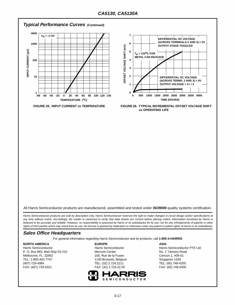
Input Current Variation with Temperature
The input current of the CA5130 Series circuits is typically5pA at 25oC. The major portion of this input current is due toleakage current through the gate protective diodes in the inputcircuit. As with any semiconductor junction device, includingop amps with a junction FET input stage, the leakage currentapproximately doubles for every 10oC increase in tempera-ture. Figure 25 provides data on the typical variation of inputbias current as a function of temperature in the CA5130.
In applications requiring the lowest practical input currentand incremental increases in current because of “warm-up”effects, it is suggested that an appropriate heat sink be usedwith the CA5130. In addition, when “sinking” or “sourcing”significant output current the chip temperature increases,causing an increase in the input current. In such cases, heat-sinking can also very markedly reduce and stabilize inputcurrent variations.
Input Offset Voltage (V IO) Variation with DC Bias vs DeviceOperating Life
It is well known that the characteristics of a MOS/FET devicecan change slightly when a DC gate source bias potential isapplied to the device for extended time periods. The magni-tude of the change is increased at high temperatures. Usersof the CA5130 should be alert to the possible impacts of thiseffect if the application of the device involves extended opera-tion at high temperatures with a significant differential DC biasvoltage applied across Terminals 2 and 3. Figure 26 showstypical data pertinent to shifts in offset voltage encounteredwith CA5130 devices (metal can package) during life testing.At lower temperatures (metal can and plastic packages), forexample at 85oC, this change in voltage is considerably less.In typical linear applications where the differential voltage issmall and symmetrical, these incremental changes are ofabout the same magnitude as those encountered in an opera-tional amplifier employing a bipolar transistor input stage. The2V differential voltage example represents conditions whenthe amplifier output stage is “toggled”, e.g., as in comparatorapplications.
Power-Supply Considerations
Because the CA5130 is very useful in single supply applica-tions, it is pertinent to review some considerations relating topower supply current consumption under both single anddual supply service. Figures 1A and 1B show the CA5130connected for both dual and single supply operation.
3
2
8
4
7
6
RL
V+
Q8
Q12
CA5130+
-
FIGURE 1A. DUAL POWER SUPPLY OPERATION
V-
CA5130, CA5130A

3-7
Dual supply operation: When the output voltage at Terminal6 is 0V, the currents supplied by the two power supplies areequal. When the gate terminals of Q8 and Q12 are drivenincreasingly positive with respect to ground, current flowthrough Q12 (from the negative supply) to the load isincreased and current flow through Q8 (from the positivesupply) decreases correspondingly. When the gate terminalsof Q8 and Q12 are driven increasingly negative with respectto ground, current flow through Q8 is increased and currentflow through Q12 is decreased accordingly.
Single supply operation: Initially, let it be assumed that thevalue of RL is very high (or disconnected), and that the inputterminal bias (Terminals 2 and 3) is such that the output termi-nal (No. 6) voltage is at V+/2, i.e., the voltage drops across Q8and Q12 are of equal magnitude. Figure 16 shows typical qui-escent supply current vs supply voltage for the CA5130 oper-ated under these conditions. Since the output stage isoperating as a Class A amplifier, the supply current will remainconstant under dynamic operating conditions as long as thetransistors are operated in the linear portion of their voltagetransfer characteristics (see Figure 15). If either Q8 or Q12 areswung out of their linear regions toward cutoff (a nonlinearregion), there will be a corresponding reduction in supply cur-rent. In the extreme case, e.g., with Terminal 8 swung down toground potential (or tied to ground), NMOS transistor Q12 iscompletely cut off and the supply current to series connectedtransistors Q8, Q12 goes essentially to zero. The two precedingstages in the CA5130, however, continue to draw modest sup-ply current (see the lower curve in Figure 16) even though theoutput stage is strobed off. Figure 1A shows a dual supplyarrangement for the output stage that can also be strobed off,assuming RL = ∞, by pulling the potential of Terminal 8 down tothat of Terminal 4.
Let it now be assumed that a load resistance of nominal value(e.g., 2kΩ) is connected between Terminal 6 and ground inthe circuit of Figure 1B. Let it further be assumed that theinput terminal bias (Terminals 2 and 3) is such that the outputterminal (No. 6) voltage is at V+/2. Since PMOS transistor Q8must now supply quiescent current to both RL and transistorQ12, it should be apparent that under these conditions thesupply current must increase as an inverse function of the RL
magnitude. Figure 22 shows the voltage drop across PMOStransistor Q8 as a function of load current at several supplyvoltages. Figure 15 shows the voltage transfer characteristicsof the output stage for several values of load resistance.
Wideband Noise
From the standpoint of low noise performance considerations,the use of the CA5130 is most advantageous in applicationswhere the source resistance of the input signal is on the orderof 1MΩ or more. In this case, the total input referred noisevoltage is typically only 23µV when the test circuit amplifier ofFigure 2 is operated at a total supply voltage of 15V. Thisvalue of total input referred noise remains essentiallyconstant, even though the value of source resistance is raisedby an order of magnitude. This characteristic is due to the factthat reactance of the input capacitance becomes a significantfactor in shunting the source resistance. It should be noted,however, that for values of source resistance very muchgreater than 1MΩ, the total noise voltage generated can bedominated by the thermal noise contributions of both thefeedback and source resistors.
Typical ApplicationsVoltage Followers
Operational amplifiers with very high input resistances, likethe CA5130, are particularly suited to service as voltagefollowers. Figure 3 shows the circuit of a classical voltagefollower, together with pertinent waveforms using theCA5130 in a split supply configuration.
A voltage follower, operated from a single supply, is shown inFigure 4, together with related waveforms. This follower circuitis linear over a wide dynamic range, as illustrated by thereproduction of the output waveform in Figure 4A with inputsignal ramping. The waveforms in Figure 4B show that thefollower does not lose its input-to-output phase sense, eventhough the input is being swung 7.5V below ground potential.This unique characteristic is an important attribute in bothoperational amplifier and comparator applications. Figure 4Balso shows the manner in which the CMOS output stage
3
2
8
4
7
6
RL
Q8
Q12
CA5130+
-
FIGURE 1B. SINGLE POWER SUPPLY OPERATION
FIGURE 1. CA5130 OUTPUT STAGE IN DUAL AND SINGLEPOWER SUPPLY OPERATION
V+
3
2
18
4
7
6
+
-
Rs
1MΩ
47pF -7.5V
0.01µF
+7.5V
0.01µF
NOISEVOLTAGEOUTPUT
30.1kΩ
1kΩBW (-3dB) = 200kHzTOTAL NOISE VOLTAGE (REFERREDTO INPUT) = 23µV (TYP)
FIGURE 2. CA5130 OUTPUT STAGE IN DUAL AND SINGLEPOWER SUPPLY OPERATION
CA5130, CA5130A

3-8
permits the output signal to swing down to the negative supplyrail potential (i.e., ground in the case shown). The digital-to-analog converter (DAC) circuit, described in the followingsection, illustrates the practical use of the CA5130 in a singlesupply voltage follower application.
9-Bit CMOS DAC
A typical circuit of a 9-bit Digital-to-Analog Converter (DAC)(see Note) is shown in Figure 5. This system combines theconcepts of multiple switch CMOS lCs, a low cost ladder net-
work of discrete metal-oxide film resistors, a CA5130 op ampconnected as a follower, and an inexpensive monolithicregulator in a simple single power supply arrangement. Anadditional feature of the DAC is that it is readily interfacedwith CMOS input logic, e.g., 10V logic levels are used in thecircuit of Figure 5.
NOTE: “Digital-to-Analog Conversion Using the Harris CD4007ACMOS lC”, Application Note AN6080.
Top Trace: OutputBottom Trace: Input
FIGURE 3A. SMALL SIGNAL RESPONSE (50mV/DIV., 200ns/DIV.)
Top Trace: Output Signal = 2V/Div., 5µs/Div.Center Trace: Difference Signal = 5mV/Div., 5µs/Div.
Bottom Trace: Input Signal = 2V/Div., 5µs/Div.
FIGURE 3B. INPUT OUTPUT DIFFERENCE SIGNAL SHOWINGSETTLING TIME (MEASUREMENT MADE WITHTEKTRONIX 7A13 DIFFERENTIAL AMPLIFIER)
FIGURE 3. CA5130 SPLIT SUPPLY VOLTAGE FOLLOWER WITH ASSOCIATED WAVEFORMS
3
2
18
4
7
6
+
-10kΩ
CC = 56pF
-7.5V
0.01µF
+7.5V
0.01µF
2kΩ
2kΩ
BW (-3dB) = 4MHz
SR = 10V/µs
25pF
0.1µF
CA5130, CA5130A

3-9
The circuit uses an R/2R voltage ladder network, with the out-put potential obtained directly by terminating the ladder arms ateither the positive or the negative power supply terminal. EachCD4007A contains three “inverters”, each “inverter” functioningas a single pole double throw switch to terminate an arm of theR/2R network at either the positive or negative power supplyterminal. The resistor ladder is an assembly of one percent tol-erance metal oxide film resistors. The five arms requiring thehighest accuracy are assembled with series and parallel combi-nations of 806,000Ω resistors from the same manufacturing lot.
A single 15V supply provides a positive bus for the CA5130follower amplifier and feeds the CA3085 voltage regulator. A“scale adjust” function is provided by the regulator outputcontrol, set to a nominal 10V level in this system. The linevoltage regulation (approximately 0.2%) permits a 9-bitaccuracy to be maintained with variations of several volts inthe supply. The flexibility afforded by the CMOS buildingblocks simplifies the design of DAC systems tailored toparticular needs.
Single Supply, Absolute Value, Ideal Full Wave Rectifier
The absolute value circuit using the CA5130 is shown in Figure6. During positive excursions, the input signal is fed through thefeedback network directly to the output. Simultaneously, thepositive excursion of the input signal also drives the outputterminal (No. 6) of the inverting amplifier in a negative goingexcursion such that the 1N914 diode effectively disconnects theamplifier from the signal path. During a negative goingexcursion of the input signal, the CA5130 functions as a normalinverting amplifier with a gain equal to -R2/R1. When theequality of the two equations shown in Figure 6 is satisfied, thefull wave output is symmetrical.
Peak Detectors
Peak detector circuits are easily implemented with theCA5130, as illustrated in Figure 7 for both the peak positiveand the peak negative circuit. It should be noted that withlarge signal inputs, the bandwidth of the peak negativecircuit is much less than that of the peak positive circuit. The
FIGURE 4A. OUTPUT WAVEFORM WITH INPUT SIGNALRAMPING
FIGURE 4B. OUTPUT WAVEFORM WITH GROUND REFERENCESINE WAVE INPUT
FIGURE 4. SINGLE SUPPLY VOLTAGE FOLLOWER WITH ASSOCIATED WAVEFORMS. (e.g., FOR USE IN SINGLE SUPPLYD/A CONVERTER; SEE FIGURE 9 IN AN6080)
3
2
81
4
7
6
+
-
10kΩ
56pF OFFSET
+15V
0.01µF
2kΩ
0.1µF
5
ADJUST
100kΩ
0V
2V/Div., 500µs/Div.
0V
0V
Top Trace: Output = 5V/Div., 200µs/Div.Bottom Trace: Input = 5V/Div., 200µs/Div.
CA5130, CA5130A

3-10
second stage of the CA5130 limits the bandwidth in thiscase. Negative going output signal excursion requires a pos-itive going signal excursion at the collector of transistor Q11,which is loaded by the intrinsic capacitance of the associ-ated circuitry in this mode. On the other hand, during a neg-ative going signal excursion at the collector of Q11, thetransistor functions in active “pull down” mode so that theintrinsic capacitance can be discharged more expeditiously.
Error Amplifier In Regulated Power Supplies
The CA5130 is an ideal choice for error amplifier service inregulated power supplies since it can function as an erroramplifier when the regulated output voltage is required toapproach 0V. Figure 8 shows the schematic diagram of a40mA power supply capable of providing regulated outputvoltage by continuous adjustment over the range from 0V to13V. Q3 and Q4 in IC2 (a CA3066 transistor array lC) func-tion as zeners to provide supply voltage for the CA5130comparator (lC1). Q1, Q2, and Q5 in lC2 are configured as alow impedance, temperature compensated source of adjust-able reference voltage for the error amplifier.
Transistors Q1, Q2, Q3, and Q4 in lC3 (another CA3086 tran-sistor array lC) are connected in parallel as the series passelement. Transistor Q5 in lC3 functions as a current limitingdevice by diverting base drive from the series pass transis-tors, in accordance with the adjustment of resistor R2.
Figure 9 contains the schematic diagram of a regulatedpower supply capable of providing regulated output voltageby continuous adjustment over the range from 0.1V to 50Vand currents up to 1A. The error amplifier (lC1) and circuitryassociated with lC2 function as previously described,although the output of lC1 is boosted by a discrete transistor(Q4) to provide adequate base drive for the Darlington con-nected series pass transistors Q1, Q2. Transistor Q3 func-tions in the previously described current limiting circuit.
Multivibrators
The exceptionally high input resistance presented by theCA5130 is an attractive feature for multivibrator circuitdesign because it permits the use of timing circuits with highR/C ratios. The circuit diagram of a pulse generator (astablemultivibrator), with provisions for independent control of the“on” and “off” periods, is shown in Figure 10. Resistors R1and R2 are used to bias the CA5130 to the midpoint of thesupply voltage and R3 is the feedback resistor. The pulserepetition rate is selected by positioning S1 to the desiredposition and the rate remains essentially constant when theresistors which determine “on period” and “off period” areadjusted.
Function Generator
Figure 11 contains a schematic diagram of a function gener-ator using the CA5130 in the integrator and thresholddetector functions. This circuit generates a triangular orsquare wave output that can be swept over a 1,000,000:1range (0.1Hz to 100kHz) by means of a single control, R1. Avoltage control input is also available for remote sweepcontrol.
The heart of the frequency determining system is an opera-tional transconductance amplifier (OTA) (see Note 9), lC1,operated as a voltage controlled current source. The output,IO, is a current applied directly to the integrating capacitor,C1, in the feedback loop of the integrator lC2, using aCA5130, to provide the triangular wave output. Potentiome-ter R2 is used to adjust the circuit for slope symmetry of pos-itive going and negative going signal excursions.
Another CA5130, lC3, is used as a controlled switch to setthe excursion limits of the triangular output from the integra-tor circuit. Capacitor C2 is a “peaking adjustment” tooptimize the high frequency square wave performance of thecircuit.
Potentiometer R3 is adjustable to perfect the “amplitudesymmetry” of the square wave output signals. Output fromthe threshold detector is fed back via resistor R4 to the inputof lC1 so as to toggle the current source from plus to minusin generating the linear triangular wave.
Operation with Output Stage Power-Booster
The current sourcing and sinking capability of the CA5130output stage is easily supplemented to provide power boostcapability. In the circuit of Figure 12, three CMOS transistorpairs in a single CA3600E (see Note 10) lC array are shownparallel connected with the output stage in the CA5130. Inthe Class A mode of CA3600E shown, a typical device con-sumes 20mA of supply current at 15V operation. Thisarrangement boosts the current handling capability of theCA5130 output stage by about 2.5X.
The amplifier circuit in Figure 12 employs feedback to estab-lish a closed-loop gain of 48dB. The typical large signalbandwidth (-3dB) is 50kHz.
NOTES:
9. See File No. 475 and AN6668.
10. See File No. 619 for technical information.
CA5130, CA5130A

3-11
FIGURE 5. 9-BIT DAC USING CMOS DIGITAL SWITCHES AND CA5130
20VP-P Input: BW (-3dB) = 230kHz, DC Output (Avg) = 3.2V1VP-P Input: BW (-3dB) = 130kHz, DC Output (Avg) = 160mV
Top Trace: Output Signal = 2V/Div.Bottom Trace: Input Signal = 10V/Div.Time base on both traces = 0.2ms/Div.
FIGURE 6. SINGLE SUPPLY, ABSOLUTE VALUE, IDEAL FULL WAVE RECTIFIER WITH ASSOCIATED WAVEFORMS
6 3 101036
4
8
36
7
9
4
10
2
3
13
8
1
512 12
1
58
1313 1 12
8 5
14
11
2
6
51
7
7
1
6
8
4
3
2
10V LOGIC INPUTS
+10.010V
LSB9 8 7 6 5 4 3 2 1
MSB
806K1%
PARALLELEDRESISTORS
10K+15V
VOLTAGEFOLLOWER
CA5130OUTPUT
LOAD
100KOFFSET
NULL
56pF
2K
0.1µF
REGULATEDVOLTAGE
ADJ.
22.1K1%
1K
3.83K1%
0.001µF
CA3085
VOLTAGEREGULATOR+15V
2µF25V
+
-
+10.010V
CD4007A“SWITCHES”
CD4007A“SWITCHES”
CD4007A“SWITCHES”
402K1%
200K1%
100K1%
806K1%
806K1%
806K1%
750K1%
806K
1%806K1%
806K1%
806K1%
(2) (4) (8)
806K1%
+
-
62
BIT12345
6 - 9
REQUIREDRATIO-MATCH
STANDARD±0.1%±0.2%±0.4%±0.8%±1% ABS
NOTE: All Resistances are In Ohms.
2
3 4
6
81
5
7
R2
2kΩ +15V
0.01µF
1N914
R3
5.1kΩ
PEAKADJUST
2kΩ100kΩ
OFFSETADJUST
20pF
CA5130
R1
4kΩ
+
-
GainR2R1------ X
R3R1 R2 R3+ +---------------------------------= = =
R3 R1X X2+1 X–
---------------- =
ForX 0.5:2kΩ4kΩ----------
R2R1------= =
R3 4kΩ 0.750.5----------
6kΩ= =
0V
0V
CA5130, CA5130A

3-12
FIGURE 7A. PEAK POSITIVE DETECTOR CIRCUIT FIGURE 7B. PEAK NEGATIVE DETECTOR CIRCUIT
FIGURE 7. PEAK-DETECTOR CIRCUITS
FIGURE 8. VOLTAGE REGULATOR CIRCUIT (0V TO 13V AT 40mA)
3
26
4
7
CA5130
+7.5V
0.01µF
+DCOUTPUT
5µF+
-100kΩ
1N914
0.01µF
-7.5V2kΩ
10kΩ+
-
6VP-P INPUT;
BW (-3dB) = 1.3MHz
0.3 VP-P INPUT;
BW (-3dB) = 240kHz
3
26
4
7
CA5130
+7.5V
0.01µF
-DCOUTPUT
5µF+
-100kΩ
1N914
0.01µF
-7.5V2kΩ
10kΩ+
-
6VP-P INPUT;
BW (-3dB) = 360kHz
0.3 VP-P INPUT;
BW (-3dB) = 320kHz
6
3
2
18
7
4
CA3086
CURRENTLIMITADJ
3Ω
R21kΩ
Q5 13
1412Q1Q2Q3Q4
10 7 3
426911 8 1 5
390Ω 1kΩ20kΩ
+
-5µF25V
56pF
ERRORAMPLIFIER
CA5130
30kΩ
100kΩ
IC1
0.01µFVOLTAGEADJUST
50kΩR1
14
13
Q5
12
62kΩ
IC3
OUTPUT0 TO 13V
AT40mA
+
-
0.01µF
+20VINPUT
2.2kΩ
+- 25µFIC2
CA3086 10 11 1, 2Q4 Q1
8, 7 6, 5Q3 Q2
6 4
+
-
+
-
NOTES:11. Regulation (no load to full load): <0.01%.12. Input Regulation: 0.02%/V.13. Hum and noise output: <25µV up to 100kHz.
1kΩ
9 3
CA5130, CA5130A

3-13
FIGURE 9. VOLTAGE REGULATOR CIRCUIT (0.1V TO 50V AT 1A)
FIGURE 10. PULSE GENERATOR (ASTABLE MULTIVIBRATOR) WITH PROVISIONS FOR INDEPENDENT CONTROL OF “ON” AND“OFF” PERIODS
6
2
3
18
7
4
4.3kΩ
1Ω
+
-43kΩ 100µF
ERRORAMPLIFIER
IC1
VOLTAGEADJUST
14
13
100µF
+55VINPUT
2.2kΩ
+-IC2
CA3086 10, 11
Q4 Q1
Q2
6
+
-
+
-
CA5130
+
-
+-
1W
3.3kΩ1W
5µF
98, 7
Q3
1, 2
35
4
1kΩ
62kΩ
Q5
12
10kΩ
Q2
Q1
50kΩ
Q3
1kΩ
2N3055
2N2102CURRENTLIMITADJUST
2N5294
2N2102
Q4
1000pF
10kΩ
8.2kΩ
OUTPUT:0.1 TO 50V
AT 1A
NOTES:14. Regulation (no load to full load): <0.005%.15. Input Regulation: 0.01%/V.16. Hum and noise output: <250µVRMS up to 100kHz.
0.01µF 40µs to 10ms
7
4
6
3
2
R1100kΩ
R2100kΩ
R3100kΩ
ON-PERIODADJUST
1MΩ
2kΩ 2kΩ
OFF-PERIODADJUST
1MΩ
+15V
0.01µF
OUTPUT
2kΩ
0.001µF0.01µF
0.1µF
1µF S1
CA5130
+
-
POSITION OF S10.001µF
0.1µF1µF
PULSE PERIOD4µs to 1ms
FREQUENCY RANGE:
0.4ms to 100ms4ms to 1s
CA5130, CA5130A

3-14
FIGURE 11. FUNCTION GENERATOR (FREQUENCY CAN BE VARIED 1,000,000/1 WITH A SINGLE CONTROL)
FIGURE 12. CMOS TRANSISTOR ARRAY (CA3600E) CONNECTED AS POWER BOOSTER IN THE OUTPUT STAGE OF THE CA5130
6
3
2
1
4
7
5
6
2
34
7
8
1
5
4
6
7
3
2
R4
270kΩ
+7.5V
VOLTAGE-CONTROLLEDCURRENT SOURCE
IC1
3kΩ3kΩ
10MΩ+7.5V
R2100kΩ
SLOPESYMMETRYADJUST
VOLTAGECONTROLLEDINPUT
-7.5V
10kΩ
10kΩR1
-7.5V
FREQUENCYADJUST(100kHz MAX)
-7.5V
+7.5V
IOIC2
+7.5V
C1
100pF
INTEGRATOR
-7.5V
56pF
CA5130+
-
CA3080A (NOTE)
+
-39kΩ
3 - 30pF
C2
ADJUSTHIGH - FREQ. DETECTOR
THRESHOLD
150kΩ
IC3
+7.5V
CA5130
+
-
R3100kΩ
AMPLITUDESYMMETRYADJUST
NOTE: See File Number 475 and AN6668 for technical information.
8
7
3
2
+15V
2kΩ CA5130
+
-
41036
4 97
6
14
750kΩ
1µF
2 11
13 1
12
58
1µF
1MΩ0.01µF
510kΩ
500µF
QP3
QN1 QN2 QN3
QP2QP1
CA3600E
AV(CL) = 48dB
LARGE SIGNALBW (-3dB) = 50kHz
RL = 100Ω(PO = 150mW
AT THD = 10%)
NOTE: Transistors QP1, QP2, QP3 and QN1, QN2, QN3 are parallel connected with Q8 and Q12, respectively, of theCA5130. See File Number 619.
(NOTE)
INPUT
CA5130, CA5130A

3-15
Typical Performance Curves
FIGURE 13. OPEN LOOP VOLTAGE GAIN AND PHASE SHIFT vsFREQUENCY
FIGURE 14. OPEN LOOP GAIN vs TEMPERATURE
FIGURE 15. VOLTAGE TRANSFER CHARACTERISTICS OFCMOS OUTPUT STAGE
FIGURE 16. QUIESCENT SUPPLY CURRENT vs SUPPLYVOLTAGE
FIGURE 17. QUIESCENT SUPPLY CURRENT vs SUPPLY VOLTAGE FIGURE 18. SUPPLY CURRENT vs OUTPUT VOLTAGE
SUPPLY VOLTAGE: V+ = 15V;V- = 0V; TA = 25oC
φ OL
3
1
1
2
3
4
4
AOL
1: CL = 9pF, CC = 0pF, RL = ∞2: CL = 30pF, CC = 15pF, RL = 2kΩ
3: CL = 30pF, CC = 47pF, RL = 2kΩ4: CL = 30pF, CC = 150pF, RL = 2kΩ
120
100
80
60
40
20
0
OP
EN
LO
OP
VO
LTA
GE
GA
IN (
dB)
-100
-200
-300
OP
EN
LO
OP
PH
AS
E (
DE
GR
EE
S)
101 102 103 104 105 106 107 108
FREQUENCY (Hz)
2
LOAD RESISTANCE = 2k Ω150
140
130
120
110
100
90
80-100 -50 0 50 100
OP
EN
LO
OP
VO
LTA
GE
GA
IN (
dB)
TEMPERATURE (oC)
22.5GATE VOLTAGE, TERMINALS 4 AND 8 (V)
OU
TP
UT
VO
LTA
GE
(V
)
17.5 2012.5 15107.52.5 50
2.5
7.5
5.0
10.0
15.0
12.5
17.5SUPPLY VOLTAGE: V+ = 15V, V- = 0VTA = 25oC
RL = 5kΩ
1kΩ2kΩ
500Ω
LOAD RESISTANCE = ∞TA = 25oC, V- = 0V OUTPUT VOLTAGE
OUTPUT VOLTAGEHIGH = V+ OR LOW = V-
15
12.5
10
7.5
5
2.5
06 8 10 12 14 16 18
TOTAL SUPPLY VOLTAGE (V)
QU
IES
CE
NT
SU
PP
LY C
UR
RE
NT
(m
A)
BALANCED = V+/2
OUTPUT VOLTAGE = V+/2V- = 0V
14
12
10
8
6
4
2
0 2 4 6 8 10 12 14 16
QU
IES
CE
NT
SU
PP
LY C
UR
RE
NT
(m
A)
TOTAL SUPPLY VOLTAGE (V)
TA = -55oC
25oC
125oC
02 2.5 3 3.5 4 4.5 5
OUTPUT VOLTAGE (V)1 1.50 0.5
SU
PP
LY C
UR
RE
NT
(µA
)
0
75
150
225
300
375
525
450
600
25oC
125oC
-55oC
V+ = 5V, V- = 0V
CA5130, CA5130A

3-16
FIGURE 19. OUTPUT VOLTAGE SWING vs LOAD RESISTANCE FIGURE 20. OUTPUT SWING vs LOAD RESISTANCE
FIGURE 21. OUTPUT CURRENT vs TEMPERATURE FIGURE 22. VOLTAGE ACROSS PMOS OUTPUT TRANSISTOR(Q8) vs LOAD CURRENT
FIGURE 23. VOLTAGE ACROSS NMOS OUTPUT TRANSISTOR(Q12) vs LOAD CURRENT
FIGURE 24. INPUT CURRENT vs COMMON MODE VOLTAGE
Typical Performance Curves (Continued)
5 6 7 8 9 10 11LOAD RESISTANCE (k Ω)
3 41 2
OU
TP
UT
VO
LTA
GE
SW
ING
(V
)
0
1
2
3
4
5
7
6
8
125oC
-55oC
V+ = 5V, V- = 0V
25oC
4 6 20 40 80 200 1000LOAD RESISTANCE (k Ω)
10.1
OU
TP
UT
VO
LTA
GE
SW
ING
(V
)
0
1
2
3
4
5
7
6
8V+ = 5V, V- = 0V
9
820.60.2
20 40 60 80 100 120 140
TEMPERATURE (oC)
-20 0-60 -40
OU
TP
UT
CU
RR
EN
T (
mA
)
0
1
2
3
4
5
7
6
8V+ = 5V, V- = 0V
SINK
SOURCE
50
10
1
0.1
0.01
0.001
VO
LTA
GE
DR
OP
AC
RO
SS
PM
OS
OU
TP
UT
TR
AN
SIS
TOR
(Q
8) (
V)
0.001 0.01 0.1 1 10 100
MAGNITUDE OF LOAD CURRENT (mA)
V- = 0VTA = 25oC
V+ = 15VV+ = 10V
V+ = 5V
V- = 0VTA = 25oC V+ = 15V
V+ = 10VV+ = 5V
50
10
1
0.1
0.01
0.001
VO
LTA
GE
DR
OP
AC
RO
SS
PM
OS
OU
TP
UT
TR
AN
SIS
TOR
(Q
12)
(V)
0.001 0.01 0.1 1 10 100MAGNITUDE OF LOAD CURRENT (mA)
10.0
7.5
5.0
2.5
0-1 0 1 2 3 4 5 6 7
INPUT CURRENT (pA)
INP
UT
VO
LTA
GE
(V
)
TA = 25oC
3
27
48
6PA
VIN
CA5130
15V TO 5V
0V TO -10V
V+
V-
CA5130, CA5130A
3-17
All Harris Semiconductor products are manufactured, assembled and tested under ISO9000 quality systems certification.
Harris Semiconductor products are sold by description only. Harris Semiconductor reserves the right to make changes in circuit design and/or specifications atany time without notice. Accordingly, the reader is cautioned to verify that data sheets are current before placing orders. Information furnished by Harris isbelieved to be accurate and reliable. However, no responsibility is assumed by Harris or its subsidiaries for its use; nor for any infringements of patents or otherrights of third parties which may result from its use. No license is granted by implication or otherwise under any patent or patent rights of Harris or its subsidiaries.
Sales Office HeadquartersFor general information regarding Harris Semiconductor and its products, call 1-800-4-HARRIS
NORTH AMERICAHarris SemiconductorP. O. Box 883, Mail Stop 53-210Melbourne, FL 32902TEL: 1-800-442-7747(407) 729-4984FAX: (407) 729-5321
EUROPEHarris SemiconductorMercure Center100, Rue de la Fusee1130 Brussels, BelgiumTEL: (32) 2.724.2111FAX: (32) 2.724.22.05
ASIAHarris Semiconductor PTE Ltd.No. 1 Tannery RoadCencon 1, #09-01Singapore 1334TEL: (65) 748-4200FAX: (65) 748-0400
S E M I C O N D U C T O R
FIGURE 25. INPUT CURRENT vs TEMPERATURE FIGURE 26. TYPICAL INCREMENTAL OFFSET VOLTAGE SHIFTvs OPERATING LIFE
Typical Performance Curves (Continued)
4000
1000
100
10
1-80 -60 -40 -20 0 20 40 60 80 100 120 140
VS = ±7.5V
TEMPERATURE (oC)
INP
UT
CU
RR
EN
T (
pA)
7
6
5
4
3
2
1
0
OF
FS
ET
VO
LTA
GE
SH
IFT
(m
V)
0 500 1000 1500 2000 2500 3000 3500 4000
TIME (HOURS)
TA = 125oC FORMETAL CAN PACKAGE
DIFFERENTIAL DC VOLTAGE(ACROSS TERMS. 2 AND 3) = 0VOUTPUT VOLTAGE = V+ / 2
DIFFERENTIAL DC VOLTAGE(ACROSS TERMINALS 2 AND 3) = 2VOUTPUT STAGE TOGGLED
CA5130, CA5130A


![[PPT]SIFAT – SIFAT CAMPURAN - addyrachmat · Web viewKonstanta Henry CO2 terlarut dalam air = 3,3 x 10⁻² mol/L atm pada 25oC Berapa kelarutan N2 di air pada 25oC dan 1 atm jika](https://img.dokumen.tips/doc/110x75/5b26dfdf7f8b9ab74e8b8294/pptsifat-sifat-campuran-addyrachmat-web-viewkonstanta-henry-co2-terlarut.jpg)
![General Specifications - Yokogawacdn2.us.yokogawa.com/GS33K55R40-50E.pdf · General Specifications [Release 5] GENERAL ... Contact](https://img.dokumen.tips/doc/110x75/5aa604cc7f8b9a1d728deb53/general-specications-specications-contents-index-release-5-general-.jpg)