Embed Size (px)
Citation preview

UNIVERSITY OF OULU P .O. Box 8000 F I -90014 UNIVERSITY OF OULU FINLAND
A C T A U N I V E R S I T A T I S O U L U E N S I S
University Lecturer Tuomo Glumoff
University Lecturer Santeri Palviainen
Postdoctoral research fellow Sanna Taskila
Professor Olli Vuolteenaho
University Lecturer Veli-Matti Ulvinen
Planning Director Pertti Tikkanen
Professor Jari Juga
University Lecturer Anu Soikkeli
Professor Olli Vuolteenaho
Publications Editor Kirsti Nurkkala
ISBN 978-952-62-1588-4 (Paperback)ISBN 978-952-62-1589-1 (PDF)ISSN 0355-3213 (Print)ISSN 1796-2226 (Online)
U N I V E R S I TAT I S O U L U E N S I SACTAC
TECHNICA
U N I V E R S I TAT I S O U L U E N S I SACTAC
TECHNICA
OULU 2017
C 618
Karoliina Jokinen
COLOR TUNING OF ORGANIC LIGHT EMITTING DEVICES
UNIVERSITY OF OULU GRADUATE SCHOOL;UNIVERSITY OF OULU,FACULTY OF INFORMATION TECHNOLOGY AND ELECTRICAL ENGINEERING
C 618
AC
TAK
aroliina Jokinen
C618etukansi.kesken.fm Page 1 Tuesday, May 16, 2017 8:58 AM


ACTA UNIVERS ITAT I S OULUENS I SC Te c h n i c a 6 1 8
KAROLIINA JOKINEN
COLOR TUNING OF ORGANIC LIGHT EMITTING DEVICES
Academic dissertation to be presented with the assent ofthe Doctoral Training Committee of Technology andNatural Sciences of the University of Oulu for publicdefence in Kuusamonsali (YB210), Linnanmaa, on 18August 2017, at 12 noon
UNIVERSITY OF OULU, OULU 2017

Copyright © 2017Acta Univ. Oul. C 618, 2017
Supervised byProfessor Risto Myllylä
Reviewed byProfessor Magnus BerggrenProfessor Kai-Erik Peiponen
ISBN 978-952-62-1588-4 (Paperback)ISBN 978-952-62-1589-1 (PDF)
ISSN 0355-3213 (Printed)ISSN 1796-2226 (Online)
Cover DesignRaimo Ahonen
JUVENES PRINTTAMPERE 2017
OpponentsProfessor Kai-Erik PeiponenResearch Professor Jukka Hast

Jokinen, Karoliina, Color tuning of organic light emitting devices. University of Oulu Graduate School; University of Oulu, Faculty of Information Technologyand Electrical EngineeringActa Univ. Oul. C 618, 2017University of Oulu, P.O. Box 8000, FI-90014 University of Oulu, Finland
Abstract
This thesis reports the investigation of color tuning of two types of organic light emitting devices,transistors (OLETs) and diodes (OLEDs). Voltage tunable two color light emission wasdemonstrated for OLETs. For OLEDs, two kinds of color tuning methods were presented. Forthese, color tuning was realized using thermal annealing which changes the light emission colorof the devices permanently.
The two color light emission of the OLETs, employing a three-layer heterostructure deviceconfiguration, occurs in red and green. The device structure was first utilized for producing redlight emission originating from a light emission layer made of Alq3:DCM that was depositedbetween the hole and electron transport layers made of DH-4T and DFH-4T, respectively. Aftermodifying the fabrication process in order to raise the device performance by acquiring smootheractive layers green light could also be produced by the devices. Green light emission originatedfrom the electron transport layer. This took place during the electron transport mode, while the redemission was apparent while hole transport was active. The color of the light emission wastherefore demonstrated as being tunable by voltage.
For OLEDs, devices with one active polymeric layer, undoped and doped, were investigated.The undoped OLEDs had the light emission layer made of blue light emitting polyfluorene PFO.The OLEDs suffered from keto-defects shifting their light emission color from blue to greenishshade, a common problem occurring in widely used blue light emitting polyfluorenes. The workconducted and reported in this thesis demonstrated that thermal annealing can be used fordiminishing this undesired green emission. For the doped OLEDs with the light emission layermade of a PFO:F8BT blend, color tuning was realized using thermal annealing as well. As a resultof exposure to thermal treatment, the light emission color of these devices which was green asfabricated was converted to white. The phenomenon behind this effect was explained by phaseseparation between the host and dopant polymers of the light emission layer.
Keywords: color tuning, organic electronics, organic light emitting diode (OLED),organic light emitting transistor (OLET)


Jokinen, Karoliina, Orgaanisten valoa emittoivien komponenttien värinsäätö. Oulun yliopiston tutkijakoulu; Oulun yliopisto, Tieto- ja sähkötekniikan tiedekuntaActa Univ. Oul. C 618, 2017Oulun yliopisto, PL 8000, 90014 Oulun yliopisto
Tiivistelmä
Tässä väitöskirjatyössä tutkitaan orgaanisten valoa emittoivien transistoreiden (OLET) ja diodi-en (OLED) värinsäätöä. Työssä tehtiin kolmikerrosrakenteisia OLETeja, jotka kykenevät emit-toimaan valoa kahdella värillä ja joiden emittointiväri on jännitesäädettävissä. OLEDien osaltatoteutettiin kaksi erilaista värinsäätömenetelmää, joissa molemmissa hyödynnettiin kuumennus-ta pysyvän värinvaihdon aikaansaamiseksi.
Tutkitut OLETit emittoivat punaista ja vihreää valoa. Aluksi tutkittiin vastaavia komponent-teja, jotka emittoivat vain punaista valoa. Näissä komponenteissa punaisen valon tuotti keskim-mäinen valoemitterinä toiminut kerros (Alq3:DCM), jonka ala- ja yläpuolella olivat aukko- jaelektronijohtavat kerrokset (DH-4T ja DFH-4T). Komponenteilla saatiin tuotettua myös vihreäävaloa, kun valmistusprosessia kehitettiin tasaisempien aktiivisten materiaalikerrosten valmista-miseksi. Vihreän valon todettiin olevan elektronijohtavan kerroksen tuottamaa. Kaksiväriemit-toiva OLET tuotti vihreää valoa ollessaan elektronijohtavassa tilassa, ja punaista valoa aukko-johtavassa tilassa, emittointivärin ollessa näin jännitesäädettävissä.
Työssä tutkittujen OLEDien valon emittointi perustui polymeerikerrokseen, joka oli toisissaOLEDeissa seostamaton ja toisissa seostettu. Seostamattomien OLEDien aktiivinen kerros olitehty sinistä valoa tuottavasta polyfluoreenista (PFO), jossa usein ilmenee keto-virheitä, joidenvuoksi PFO:sta tehtyjen OLEDien valo muuttuu sinisestä vihertäväksi. Työssä osoitettiin, ettäkuumennusta voidaan käyttää sinisen emittointivärin palauttamiseen. Seostettujen OLEDien(PFO:F8BT) osalta kuumennusta käytettiin komponenttien emittointivärin muuttamiseksi alku-peräisestä emittointiväristä vihreästä valkoiseksi. Tämä ilmiö selitettiin valoa emittoivan kerrok-sen polymeerien välisellä faasierkaantumisella.
Asiasanat: orgaaninen elektroniikka, orgaaninen valoa emittoiva diodi (OLED),orgaaninen valoa emittoiva transistori (OLET), värin säätö


This one is tricky. You have to use
imaginary numbers, like eleventeen...
- Calvin & Hobbes

8

Acknowledgements
This thesis is a result of my PhD studies carried out at the Optoelectronics andMeasurement Techniques Laboratory at the University of Oulu during 2010–2017.I appreciate all the support given to me and my work, and I would like to thank thegreat people I worked with. I wish to express my deepest gratitude to my supervisor,Professor Risto Myllylä for his continuous support and guidance, which made myresearch work and graduation possible. I acknowledge Professor Ghassan Jabbour for theinteresting project and for the advice at the beginning of my work, and Dr. Hanna Jabbourfor the valuable support and advice, and for introducing me to organic electronics.I want to give a huge thanks to Dr. Alexander Bykov for the cooperation and forsharing all the effort and joy of making our OLETs and OLEDs shine. Many thanks toDr. Rafal Sliz for his extensive support from day one of my work, and to Professor JyrkiLappalainen for patiently giving me an opportunity to learn how the MEIS sensors reallywork. I sincerely thank Dr. Alexey Popov and MSc Kari Remes for their work, whichhelped me move forward with my own. I acknowledge Professor Tapio Fabritius forsupporting my work, and Professors Olli Silven and Heli Jantunen for their advice andencouragement. Dr. Hannu Sorvoja, Workshop Laboratory Foreman Vesa Kaltio, andSenior Laboratory Technicians Pekka Moilanen and Kai Metsäkoivu at the NMT centerare all acknowledged for their efforts in keeping my work progressing, and PrimaryStudent Counselor Varpu Pitkänen for keeping my study record in order. I am thankfulthat I had a chance to receive advice from and to host such a talent as Professor JanaZaumseil during my studies. I am also grateful to the excellent reviewers of my thesis,Professors Kai-Erik Peiponen and Magnus Berggren.
For all the fun, talks and laughs, a huge, huge thanks to Rafal, Janne, and Jacub,and for our girls group, Meng, Eija, and Varpu, and all the other great people I had achance to work with. Next, I cannot give enough thanks to Annamari and Jenni for thewonderful peer support and company when writing my thesis. It is amazing how youcame up with ”Shut Up and Write!”, something that is useful yet fun and at just the righttime for me. I guess it really was about making the world a better place. Bubbles arewell earned–well done us! Many thanks also to Sofia for checking ”Tiivistelmä” and forsharing experiences.
9

I want to warmly thank my family for everything; for all the support and for beingthere. And finally, the greatest thanks for Jonne for loving, living, and enjoying life withme.
For financial support, I thank the graduate schools GETA and UniOGS, Riitta jaJorma J. Takasen säätiö, Tekniikan edistämissäätiö, Emil Aaltosen säätiö, Ulla Tuomisensäätiö, Walter Ahlströmin säätiö, and Tauno Tönningin säätiö.
Oulu, November 9th 2016
10

Abbreviations and symbols
AC Alternating currentAFM Atomic force microscopyAlq3 Tris(8-hydroxyquinolinato)aluminiumCIE Commission internationale de l’éclairageDC Direct currentDH-4T α,ω-dihexyl-quaterthiopheneDFH-4T α,ω-diperfluorohexyl-quaterthiopheneDCM 4-(dicyanomethylene)-2-methyl-6-(p-dimethylaminostyryl)-4H-pyranEQE External quantum efficiencyF8BT Poly[(9,9-di-n-octylfluorenyl-2,7-diyl)-alt-(benzo[2,1,3]thiadiazol-4,8-diyl)HOMO Highest occupied molecular orbitalHTL Hole transport layerITO Indium-tin-oxideLCD Liquid crystal displayLED Light emitting diodeLEL Light emission layerLET Light emitting transistorLUMO Lowest unoccupied molecular orbitalMEIS Metal-electrolyte-insulator-semiconductorOFET Organic field-effect transistorOLED Organic light emitting diodeOLET Organic light emitting transistorPFO Poly(9,9-di-n-octylfluorenyl-2,7-diylPEDOT:PSS Poly(3,4-ethylenedioxythiophene):poly(styrenesulfonate)PMMA Poly(methyl methacrylate)RGB Red, green, blueSPYIN 2’,7’-ditert-butyl-N,N-diphenyl-7-(4-(1-phenyl-1H-benzoimidazol-2-yl)-
phenyl)-9,9’-spirobi[fluorene]-2-amineTFT Thin film transistor
Ci Capacitance of a dielectrice Electron
11

Eg Energy bandgaph HoleId Drain currentIe f f Current efficiencyL Channel lengthVd Drain voltage i.e. drain-source voltageVg Gate voltage i.e. gate-source voltageVth Threshold voltageW Channel width
µsat Saturation mobility (of the charge carriers)
12

List of original articles
This thesis is based on the following articles, which are referred to in the text by theirRoman numerals (I–V):
I Jokinen K, Popov A, Lappalainen J, Sliz R, Fabritius T, Kordas K, Myllylä R and Vasiliev A(2016) Performance enhancement of polymer electrolyte MEIS hydrogen sensor by DC-biasing. IEEE Sensors Journal 16: 5292 – 5297.
II Jokinen K, Bykov A, Sliz R and Myllyla R (2012) Behaviour of electron and hole currentsin a 3-layer heterostructure OLET. Proc. SPIE 8435, Organic Photonics V: 84351L.
III Jokinen K, Bykov A, Fabritius T and Myllylä R (2014) Two-color emission in three-layerheterostructure OLETs. Proc. SPIE 9183, Organic Light Emitting Materials and DevicesXVIII: 91831Q.
IV Jokinen K, Bykov A, Sliz R, Remes K, Fabritius T and Myllylä R (2015). Luminescenceand spectrum variations caused by thermal annealing in undoped and doped polyfluoreneOLEDs. Solid-State Electronics 103: 184 – 189.
V Jokinen K, Bykov AV, Sliz R, Remes K, Fabritius T and Myllylä R (2015) Light emissioncolor conversion of polyfluorene-blend OLEDs induced by thermal annealing. IEEETransactions on Electron Devices 62: 2238 – 2243.
For Article I, the author developed the idea of DC-biasing for enhancing the sensorperformance, analyzed the experiment results together with J. Lappalainen, performedthe literature review and wrote the manuscript. A. Popov performed the experimentalpart of Article I. The author performed most of the experiments that were done incooperation with A. Bykov for Articles II–V. For those works, the author conducted theliterature reviews and wrote the manuscripts of the publications. A. Bykov calculatedcharge carrier mobilities and threshold voltages for the OLETs for Articles II–III. R. Slizperformed atomic force microscope (AFM) measurements for Articles II & V. K. Remesprepared polymeric solutions for the OLED-fabrication for Articles IV & V. Co-authorsreviewed and improved the manuscripts before publication.
13

14

Contents
AbstractTiivistelmäAcknowledgements 9Abbreviations and symbols 11List of original articles 13Contents 151 Introduction 172 Organic light emitting diodes and transistors 19
2.1 Organic light emitting diodes . . . . . . . . . . . . . . . . . . . . . . . . . . . . . . . . . . . . . . . . . . 212.1.1 Device structures and operation . . . . . . . . . . . . . . . . . . . . . . . . . . . . . . . . . 212.1.2 Characterization . . . . . . . . . . . . . . . . . . . . . . . . . . . . . . . . . . . . . . . . . . . . . . . 22
2.2 Organic light emitting transistors . . . . . . . . . . . . . . . . . . . . . . . . . . . . . . . . . . . . . . 232.2.1 Device structures and operation . . . . . . . . . . . . . . . . . . . . . . . . . . . . . . . . . 232.2.2 Significance of the dielectric layer . . . . . . . . . . . . . . . . . . . . . . . . . . . . . . .262.2.3 Experiments on the dielectric layer . . . . . . . . . . . . . . . . . . . . . . . . . . . . . . 272.2.4 Characterization . . . . . . . . . . . . . . . . . . . . . . . . . . . . . . . . . . . . . . . . . . . . . . . 29
3 Color tuning of organic light emitting devices 313.1 OLETs with light emission color tunable by voltage . . . . . . . . . . . . . . . . . . . . . 31
3.1.1 Two color light emitting three-layer OLETs . . . . . . . . . . . . . . . . . . . . . . 343.2 Color tuning of OLEDs . . . . . . . . . . . . . . . . . . . . . . . . . . . . . . . . . . . . . . . . . . . . . . . 39
3.2.1 Emission color enhancement of undoped OLEDs . . . . . . . . . . . . . . . . . 413.2.2 Color conversion of doped OLEDs . . . . . . . . . . . . . . . . . . . . . . . . . . . . . . 42
4 Discussion and conclusion 49References 53Original publications 61
15

16

1 Introduction
Organic electronics is a rather new, vastly expanding field of technology. It is basedon the use of organic semiconductors as active materials in electronic devices insteadof traditionally used inorganic semiconductors, such as silicon. In this thesis, organicelectronic devices with a light emitting property are examined. The main focus areorganic light emitting diodes (OLEDs) and transistors (OLETs). Of these, OLETspresent a relatively new type of devices with their development being still at the researchstage, whereas OLEDs, are already widely available in commercial applications. Today,OLED displays are commonly utilized in smart phones [1, 2] and OLED-TVs are on themarket rivaling LED-backlit liquid crystal display (LDC) TVs [3–5]. OLED technologyfirst made it possible to bring displays with big screen sizes that were not found onLCDs to consumer markets, when in 2015 LG launched models reaching up to 77 inch[3]. In addition to the ability to produce large-area devices at lower costs than before,OLED-TVs have also other advantages such as the capability of turning single pixels offso to produce genuine black. Also flexible, ultra-thin (approx. 0.1 inch) or transparentdisplays could be produced but this far these have been limited to exhibitions. The otherassets over the LCD-technology include high brightness, high contrast ratios, wideviewing angles, low response times and low power consumption [6–9].
Much of the interest towards organic electronics stems from the opportunity ofgaining low-cost products [10]. Materials and processing costs are reduced in comparisonto conventional silicon based technology [10, 11]. Organic semiconductors, whichmay consist of materials such as polymers, are relatively easy to synthetize and theyalso do not require the high processing temperatures that are needed for inorganicsemiconductors [12]. In addition, methods such as standard printing techniques canbe applied for their fabrication. For these reasons the costs are reduced for organicelectronics, but besides the low-cost, it is also possible to achieve new kinds of deviceproperties that are hard or even impossible to achieve with inorganic electronics. Thesekinds of properties include e.g. flexibility, low weight, thinness and large device area[13].
Organic electronics also however faces many disadvantages that limit deviceperformance, and hence, commercialization of applications. These downsides includelow charge carrier mobility and life-time problems. Also the fabrication process,
17

although simpler, is less robust than for inorganic semiconductors. By and large, organicelectronics currently competes with silicon-based electronics above all on price insteadof quality. Therefore, active research work is needed to bridge the gap and to bring outthe advantages of organic electronics.
Color tuning is a feature that could offer an advantage for organic light emittingdevices over the inorganic ones. This is due to the benefits of the inherent properties oforganic electronic materials and the potential for efficiently processing them to gainthis feature. This thesis utilizes these advantages in investigating color tuning featurein OLEDs and OLETs. Concerning OLETs, devices with voltage tunable color ofthe light emission are examined. For tuning the emission color of OLEDs, two kindsof modifications are realized to change their light emission color permanently. Themodifications are executed to enhance the color purity of the OLEDs and to converttheir light emission color. In addition, DC-biasing of a metal-electrolyte-insulator-semiconductor (MEIS) gas sensor with polymer electrolyte is demonstrated as a methodfor enhancing performance of these types of sensors. The method is also proposedas a potential approach for enhancing performance of other electrolyte-gated devices,including transistors.
This thesis includes five articles (I-V) that are reviewed by the introductory partcomprised of four chapters. This Introduction is followed by the chapter ”Organic lightemitting diodes and transistors” that is a lead-in to the operation principles of OLEDsand OLETs and suggests the method that could be used for reducing the switching speedof electrolyte-gated OLETs. It aims to provide background information and reasoningfor the research into the color tuning feature, for which the results attained in the thesis,are presented in the chapter ”Color tuning of organic light emitting devices”. Thatchapter also presents a literature review on color tuning of organic light emitting devices.Finally, the chapter ”Discussion and conclusion” gathers and analyzes the results of thethesis. Future work for taking the research forward is also proposed.
18

2 Organic light emitting diodes andtransistors
This thesis deals with two types of organic light emitting devices, OLEDs and OLETs.To differentiate them from the corresponding inorganic light emitting diodes (LEDs) andtransistors (LETs), the devices are considered to be organic when the active materialsresponsible for charge transfer and light generation are made of organic semiconductors.These kinds of organic compounds can be e.g. polymers, which are traditionally knownas insulators. However, in the mid-1970s Alan Heeger, Alan MacDiarmid, and HidekiShirakawa showed that the conductivity of polymers can be varied from being aninsulator to becoming a conductor by electrochemical doping [14]. The work createdthe grounds for the field of organic electronics and brought them a Nobel prize in theyear 2000 [15–17].
The basis for the electric conductivity and semiconductivity of organic semiconduc-tors originates from overlapping π-orbitals that allow for delocalization of electroniccharges along the molecule or polymer. This means the alternation of single and doublebonds between the carbon atoms of the molecule chains, which in turn leads to thedelocalization of the electrons. When such molecules with delocalized electronicsystems are closely packed together, their interaction creates continuous energy bandsthat allow the transfer of unbound electrons [15, 18]. Long-range transport is thenpossible and includes hopping of charges across barriers at domain-domain interfaces.For organic semiconductors the energy bands are referred to as the highest occupiedmolecular orbital (HOMO) and the lowest unoccupied molecular orbital (LUMO).Electrons transfer on LUMO, and holes, which can be seen as empty electron states,transfer on HOMO. Light emission takes place when, due to coulomb attraction, anelectron situated on LUMO creates a pair, an exciton, with a hole on HOMO. The energyequivalent for the bandgap of the molecular orbitals is then released as a photon [19] asdepicted in Figure 1.
Organic semiconductors are classified into three categories. The earlier mentionedpolymers form one of the classes, while small molecules and natural or nature-inspiredmaterials form the other two classes [20, 21]. Small molecules are low molecular weightmaterials. This is in contrast to polymers that consist of long molecular chains. Natureand nature-inspired materials are not widely researched as active materials for organic
19

Fig. 1. Illustration of light emission generation in organic light emitting semiconductors:holes (+) and electrons (–) are transferred at their respective energy levels, HOMO and LUMO,then bind as an exciton, and subsequently, recombine releasing a photon. Eg stands for theenergy bandgap between the LUMO- and HOMO-levels that determines wavelength, hencecolor, of the light emission.
electronics devices, but should be noted for their potential to generate environmentallyfriendly electronics in the future [21]. Small molecules and polymers are used as activematerials in the devices investigated in this thesis.
Different preparation techniques are required for small molecules and polymers. Theadvantage of polymers is that they can be synthetized to be soluble in common solvents.This makes fabrication possible using solution processing techniques, including e.g.
printing, that are readily scalable for mass manufacturing. The solution processingmethod applied in this thesis in the fabrication of polymer-based OLEDs is spin coating.This is a general method used in the research stage for investigation of devices, whichare desired to be fabricated using higher throughput fabrication methods in the future.
Small molecules are usually deposited by vacuum thermal evaporation that is thetechnique used in Articles II and III of this thesis for fabrication of the OLETs, whoseactive layers are made of small molecules. Generally, thermal evaporation has lowerthroughput than solution processing methods, but it can also be adapted to roll-to-rollmanufacturing likewise many printing methods. It is a well-established technique usedfor manufacturing commercial OLED displays [22, 23]. Its significant benefit is that itallows the deposition of numerous layers in a stack. That is more of a challenge to do bysolution processing methods, where orthogonal solvents must be used in deposition of
20

successive layers to prevent dissolving the previous layer when depositing the next one[10, 24].
2.1 Organic light emitting diodes
It was in the end of 1980s, when the first OLEDs were realized. Ever since, developmentof OLEDs has been rapid and nowadays they represent the most developed type oforganic electronic device when it comes to commercial applications [20]. So far displaytechnology has been the major application field with lighting applications prospected asa follower.
2.1.1 Device structures and operation
In OLEDs, holes and electrons are injected from contact electrodes, transported throughthe organic layer(s), then forming excited states, which finally recombine to emitphotons. The contact electrodes are chosen so that their work functions support easyinjection of charge carriers to the device. Thereby, the positively biased anode needsto be a high work function material for gaining efficient injection of holes into theHOMO-level of the successive layer. Respectively, for the negatively biased cathodecontact, a low work function material should be used to obtain the optimal injectionof electrons to the LUMO level of the adjacent material layer. One of the electrodesalso has to allow light to pass through it. Usually that is the anode contact, made ofindium-tin-oxide (ITO) which is a high work function material and transparent tovisible light. The cathode contact electrodes are typically made of material alloys orstacked layers such as Mg:Ag or LiF/Al.
The first successful OLEDs that were demonstrated by C. W. Tang and S. A. Van Slykefrom Eastman Kodak’s research laboratories in 1987 [25] consisted of two organic semi-conducting layers sandwiched between contact electrodes. One of the active layers tookcare of hole transport, while the other one made of tris(8-hydroxyquinoline)aluminum(Alq3) provided electron transport and light generation. Ever since then various OLED-structures have been presented. At its simplest, OLEDs with just one layer, capableof transporting both holes and electrons and emitting light, can be built. However,more layers are typically needed to enhance device operation. For example, poly(3,4-ethylenedioxythiophene):poly(styrenesulfonate) (PEDOT:PSS) is generally used as abuffer layer for aiding hole injection [26, 27] and smoothening the roughness of the
21

contact electrode which is usually made of ITO [28]. Besides the kind of two-layerdevices presented by C. W. Tang and S. A. Van Slyke [25], where one of the layers isresponsible for light emission, two layer devices without an actual light emission layercan also be built [29]. In these devices light emission takes place at the interface of thehole and electron transport layers. Furthermore, multilayer OLEDs are also often built,e.g. so that a light emission layer is deposited between layers dedicated to the transferof holes and electrons. With multilayer devices, optimization of device performancetargeting for high efficiency light emission can be pursued [29, 30]. The total thicknessof the active layers is usually in the order of 100 nm.
Light emission layers can be made of a single material but it is also common to dopethem with a guest material with a smaller energy band gap. The doping approach isdone to pursue higher light emission efficiencies and to red-shift the light emission colorof the devices [30, 31]. The host material is responsible for transport of charges andtransfer of excited states, while light emission takes place from the dopant materialwhich excitons are transferred to from the host material by Förster energy transfer. Thecolor of the light emission is therefore determined by the dopant material. This makesblue light emitting materials of high importance. Since these have the largest energybandgap of all the light emitting materials, OLEDs in the other colors can be producedby doping them.
2.1.2 Characterization
OLEDs are tested for luminance, efficiency, turn-on voltage and their light emissionspectrum, in order to characterize their performance. Luminance, that is the brightnessof the light emission, aims to describe how brightly the human eye sees the lightemission. This depends on the amount of photons produced by the device, but also on theluminosity function describing the dependency of the visual perception on the spectrumof the light emission [32]. As sensitivity of the eye is at its strongest (in daylight) forlight at a wavelength of 555 nm, which corresponds to green, light from a source in thiscolor is experienced as being brighter than blue or red light at the same photon flux. It isstandard practice to present a light emission spectrum with peak wavelength as part ofOLED specifications, but in addition a Commission Internationaled’Eclairage (CIE)color space graph is also used to give further information about the color of the lightemission as it is perceived by the human eye [33].
22

Turn-on voltage is simply determined as the voltage required to produce a certainluminance level, usually 10 cd/m2 or 100 cd/m2 in the forward scan of the bias voltage.OLED efficiency is usually described as current efficiency or quantum efficiency.Current efficiency, which is the measure of efficiency used in this thesis for OLEDs,describes the maximum value of luminance per current unit showed by the device. Asfor quantum efficiency, this is a direct measure of the number of emitted photons by thenumber of injected electrons. External quantum efficiency (EQE) takes into accountonly the photons escaping from the OLED, whereas internal quantum efficiency countsall the generated photons regardless of whether they are expelled from the device aslight emission or not.
2.2 Organic light emitting transistors
The first OLET was realized in 2003 by Hepp et al. [34], roughly 15 years after thecreation of the first OLED. A unique feature of OLETs is the combination of theswitching property of transistors with the light emitting property of OLEDs. Thiscombination of properties is advantageous for creating numerous applications. Forinstance, in OLED-displays a thin-film-transistor (TFT) back panel is needed forswitching in order to drive the operation of the OLEDs. Hence, the integration of theswitching property in the light emitting device, as done in OLETs, could simplifydisplay fabrication [8, 35]. Whereas OLED products have established markets, OLETsare still at a research stage pursuing potential applications on lighting and opticalcommunication systems in addition to display technology [35]. Furthermore, electricallypumped organic lasers have been proposed [36, 37] but have not been successfullycreated yet. OLETs are also of scientific interest because they provide a tool for study offundamental properties of charge injection, transport and excitation, and light emissionin organic materials [38–41]. For this purpose especially a horizontal device structure isbeneficial due to direct access for optical probing of electroluminescence.
2.2.1 Device structures and operation
Figure 2 presents a series of OLETs with a horizontal device structure, which is thetype of OLET structure being of subject in this thesis. As in the figure, the OLETstypically have three electrodes: a source, a drain and a gate. Although, OLETs with fourelectrodes with a split gate architecture have also been presented [42]. A source electrode
23
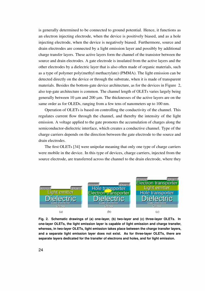
is generally determined to be connected to ground potential. Hence, it functions asan electron injecting electrode, when the device is positively biased, and as a holeinjecting electrode, when the device is negatively biased. Furthermore, source anddrain electrodes are connected by a light emission layer and possibly by additionalcharge transfer layers. These active layers form the channel of the transistor between thesource and drain electrodes. A gate electrode is insulated from the active layers and theother electrodes by a dielectric layer that is also often made of organic materials, suchas a type of polymer poly(methyl methacrylate) (PMMA). The light emission can bedetected directly on the device or through the substrate, when it is made of transparentmaterials. Besides the bottom-gate device architecture, as for the devices in Figure 2,also top-gate architecture is common. The channel length of OLETs varies largely beinggenerally between 10 µm and 200 µm. The thicknesses of the active layers are on thesame order as for OLEDs, ranging from a few tens of nanometers up to 100 nm.
Operation of OLETs is based on controlling the conductivity of the channel. Thisregulates current flow through the channel, and thereby the intensity of the lightemission. A voltage applied to the gate promotes the accumulation of charges along thesemiconductor-dielectric interface, which creates a conductive channel. Type of thecharge carriers depends on the direction between the gate electrode to the source anddrain electrodes.
The first OLETs [34] were unipolar meaning that only one type of charge carrierswere mobile in the device. In this type of devices, charge carriers, injected from thesource electrode, are transferred across the channel to the drain electrode, where they
(a) (b) (c)
Fig. 2. Schematic drawings of (a) one-layer, (b) two-layer and (c) three-layer OLETs. Inone-layer OLETs, the light emission layer is capable of light emission and charge transfer,whereas, in two-layer OLETs, light emission takes place between the charge transfer layers,and a separate light emission layer does not exist. As for three-layer OLETs, there areseparate layers dedicated for the transfer of electrons and holes, and for light emission.
24

recombine with the opposite type of charges to generate light. Therefore, in unipolarOLETs, light emission always takes place in close proximity to the drain electrode. It isbased on formation of a cloud of opposite charges in the channel very close to the drainelectrode that causes the transferred charges to recombine instead of escaping to thedrain electrode [43, 44].
In ambipolar OLETs, both types of charge carriers are mobile and transport alongthe channel. The light emission zone can be controlled by the bias voltage to take placeanywhere between the drain and source electrodes [39, 45]. Light emission takes place atthe location where the accumulation layers of holes and electrons overlap and it usuallyappears as a narrow line with a width of a couple of micrometers [39, 45, 46]. However,light emission covering the full length of the channel has also been demonstrated forthree-layer heterostructure OLETs [47].
The ability to adjust the location of the light emitting zone makes it possible to reachhigher light emission efficiencies for ambipolar OLETs than for unipolar OLETs. Thisis because all the charges must recombine [48], when the light emission takes place inthe channel aside from the electrodes. This in turn stems from the fact that chargescannot escape to the counter electrode through an accumulation layer of opposite typecharges in a length of micrometers [39]. Exciton quenching and photon losses caused bythe source and drain electrodes can also be minimized by adjusting the light emission totake place within the channel a distance away from electrodes [39, 41].
As OLEDs, OLETs too can at their simplest be fabricated with a single active layerthat is capable of light emission and charge transfer. Importantly, ambipolar OLETscan also be made with a single active layer [39, 45, 49]. In this case a light emittingmaterial with a balanced charge transfer capability for holes and electrons is required.This is possible to achieve and the best EQE for OLETs has been published for a singlelayer polymer OLET produced by Gwinner et al. [50]. Alternatively, a heterojunctionapproach can be implemented for ambipolar single layer OLETs by making the layer amixture of two unipolar materials with hole and electron transport capabilities [51–53].This was also the means exploited for realization of the first ambipolar OLET [51].Additionally, multilayer OLETs have been widely studied [41, 44, 54]. A heterojunctionapproach has been applied to two-layer OLETs so that light emission takes place inbetween the hole and electron transport layers [55], as in the two-layer OLET depictedin Figure 2. Using three-layer OLETs, high efficiency performance competing that ofequivalent OLEDs was demonstrated by Capelli et al. [41]. With an EQE of 5% thisdevice was considered the most efficient OLET until Gwinner et al. [50] achieved single
25

layer OLETs with efficiency as high as 8%, and even over 12% for an OLET with ahalf-sphere integrated on top of the device to enhance light outcoupling.
2.2.2 Significance of the dielectric layer
Obtaining efficient OLETs requires semiconducting materials with charge transport andlight emission capabilities, and electrode materials of suitable work functions allowinglow barrier charge injection. Besides these prerequisites a dielectric layer plays animportant role in the operation of OLETs. Due to its capacitance it impacts the operationvoltage, which unfortunately tends to be high for OLETs. This is due to the limitedcharge transfer mobility and relatively large charge transfer distances combined with thefact that fabrication of very thin defect free dielectrics is challenging, especially bymeans of solution processing.
The call to lower operation voltages makes solid electrolytes an attractive alternativeto be used in OFETs [56–59], and also of great interest in OLETs. Because of theformation of electrolyte double layers, they offer high capacitances, and hence low-voltage operation, independent of the thickness of the materials layer. This combinedwith the benefit that they can be made of solution processable materials e.g. ofpolymers, makes them a promising candidate especially for printed electronics [60–62].Unfortunately, they suffer from the drawback of slow ion mobility which can severelylimit the switching speed of the devices. This problem might, however, be solved bychoosing materials of higher ion conductivity or by further development of materials [60].Potentially, the problem could also be circumvented by using DC-biasing in parallel withthe AC-driving signal. This would be to support the formation of permanent electrolytedouble layers, as was proposed in Article I of this thesis, based on the demonstrationmade on a capacitor type of metal-electrolyte-insulator-semiconductor (MEIS) gassensor.
Besides the high capacitance of the dielectric, the quality of its interface with thecharge transfer layer is essential to be of good quality. This also requires the right choiceof material to avoid trapping the charges. Before this was well comprehended, there wasa common understanding that most of the organic semiconductors naturally lacked thecapability of transporting electrons. In 2005, Chua et al. [63] however demonstratedthat the equal capability of transporting holes and electrons can be achieved if thesemiconductor-dielectric interface is made so that it is free of electron traps, in otherwords, that it supports the transfer of electrons.
26

In Article II of this thesis, the importance of the dielectric was further researched.Three layer heterostructure OLETs were fabricated with two different kinds of dielectriclayers. In both of the cases the dielectric layer was made of PMMA by spin coating.The OLETs however showed drastically different transport properties. For the first setof OLETs, the dielectric layer was fabricated using a self-made solution of PMMAdissolved in toluene and for the second set, a ready-prepared, commercially availablesolution of PMMA in ethyl lactate was used.
2.2.3 Experiments on the dielectric layer
Figure 3 presents the structure of the OLETs investigated. They were made according toa three-layer heterostructure device configuration that was first presented by Capelli et
al. [41]. The OLETs were fabricated on ITO coated glass substrates. Two alternativetypes of solutions of PMMA were used in the fabrication of the dielectric layer: 1) a self-prepared solution of PMMA (Mw ∼ 98.5 kDa, Sigma-Aldrich) mixed in toluene with6 wt-% and 2) a ready-prepared solution of PMMA (Mw = 600 kDa) in ethyl lactate witha concentration of 6 wt-% purchased from AllResist GmbH. The layers were fabricatedby spin coating. Then, the layers made of PMMA/toluene solution were annealed in avacuum oven for 7 and half hours at 170 ◦C without introducing a vacuum. The layersmade of PMMA/ethyl lactate solution were annealed at 130 ◦C for 12 hours at a pressureof ∼ 3 Torr. In both cases the thickness of the layers was approximately 450 nm and thefilm qualities were smooth when inspected by optical microscope.
Fig. 3. A schematic drawing of the investigated three-layer heterostructure OLETs.
The active layers of the OLETs consisted of hole and electron transport layers with alight emission layer sandwiched between them. The layers were deposited by thermalevaporation. Charge transport layers were made of thiophene derivatives purchased from
27

(a) (b)
Fig. 4. Transfer characteristics curves of the three-layer OLETs with dielectric prepared froma solution of PMMA dissolved in (a) toluene and (b) ethyl lactate.
Polyera Corp. The hole transport layer was made of α,ω-dihexyl-quaterthiophene (DH-4T) and the electron transport layer was made of α,ω-diperfluorohexyl-quaterthiophene(DFH-4T). The evaporation rate of the charge transfer layers was 3 Å/ min. Thelight emission layer was fabricated from Alq3 as the host material and was dopedwith 4-(dicyanomethylene)-2-methyl-6-(p-dimethylaminostyryl)-4H-pyran (DCM).The evaporation rates of Alq3 and DCM were 2 Å/s and 3 Å/min so that a dopingconcentration of ∼ 3% was achieved. The thicknesses of the hole, light emitting andelectron transport layers were 7, 40 and 25 nm, respectively. The source and drainelectrodes were evaporated through a shadow mask from LiF (1.2 nm) and Al (100 nm)to form a channel with a length of 130 µm and a width of 10 cm. Device fabrication andcharacterization were performed in a nitrogen atmosphere without exposing the devicesto ambient conditions. Light emission was observed visually.
The graphs presented in Figure 4 show the transfer characteristics curves of threelayer OLETs made of PMMA/toluene and PMMA/ethyl lactate solutions. Based on thecurve shapes, the first of the curves, corresponding to dielectric made of PMMA/toluene,shows a very negligible hole current with a pronounced electron current. The situationchanged however for the devices with dielectric made of PMMA/ethyl lactate, whichhad a stronger hole current than electron current. What was important, was that thedevices with dielectric made of PMMA/ethyl lactate showed light emission, whereas nolight was observed from the devices with dielectric made of PMMA/toluene. As the
28

active layers and also the fabrication procedures were similar, the differences betweenthe hole and electron currents of the devices, was attributed to the dielectric.
2.2.4 Characterization
As well as for OLEDs also for OLETs luminescence, efficiency and color of the lightemission are important device specifications. The measures of the properties of lightemission and its color are similar for the OLETs as for the OLEDs. However, sincethe OLET technology is not a well-established, estimation and analysis of the overallperformance of devices is often more feasible than gaining e.g. maximal brightness ofthe light emission. In addition, light emission colors of OLETs are primarily restricted bythe limited (commercial) availability of materials than set by the needs of an application.Furthermore, because OLETs can rival OLEDs in terms of the efficiency of the lightemission, EQE has become a merit of interest for OLETs, as well as finding a means ofachieving high EQE.
Charge carrier mobility is an important measure of operation performance ofOLETs. The mobility characterizes the velocity of a charge carrier inside a material asit experiences an electric field, thus it determines the switching speed of the OLETstogether with the channel length. Thereby, mobilities are of high significance forperformance, when pursuing applications requiring pulsing of light emission.
Charge carrier mobility is usually considered as a saturation field-effect mobilitythat can be estimated e.g. by driving an OLET in a unipolar mode so that the drainvoltage (Vd) and gate voltage (Vg) are set equal, |Vd |= |Vg|. For the saturation mode, thedrain-source current is described by Equation 1 from which the mobility of the chargecarriers in question can be calculated, i.e. this is done separately for holes and electrons.In the equation [39, 64] W is the channel width, Ci is the capacitance of the dielectric,µsat is the saturation mobility, L is the channel length and Vth is the threshold voltage.h and e refer to holes and electrons, respectively. Also the threshold voltages can bederived using Equation 1. Small threshold voltages and high mobility are desired forobtaining low operation voltage. Both of these should also be in balance for holes andelectrons to reach ambipolar device operation.
Id,sat =W ·Ci ·µe/h
sat
2L· (Vg−V e/h
th )2 (1)
29

30

3 Color tuning of organic light emittingdevices
The first works on OLEDs with light emission color tuned by voltage were publishedby the mid-1990s [65–67]. In those works, the color tuning features were based onblending light emitting materials with different emission colors in a single light emissionlayer. The approach was visionary, although, the colors were turned on top of each otherand there was no ability to switch from one color light emission to another.
In addition to the single layer, blended light emitter with voltage-dependent lightemission color [65–69], an approach utilizing stacked light emission layers of differentemission colors [70, 71] has also been applied in order to realize multicolor OLEDswith voltage tunable light emission color. Other implemented methods [72] includecolor absorption filters on white OLEDs [73–75], fluorescent color conversion layers onblue OLEDs [76, 77] and adjacent [78, 79] or vertically stacked OLED pixels [80–82]of different colors and a combination of these [83]. These methods, whose operationprinciples are presented in Figure 5, lack however the ability to achieve voltage tunablelight emission color from a single OLED.
Whereas there are various works regarding multicolor OLEDs with voltage tunablelight emission color, only a few works on OLETs with similar functions have beenpublished. This is despite the fact that OLETs provide the opportunity for moving thelight emission zone by voltage [39, 43, 45], a feature that is advantageous for producingmulticolor light emission.
3.1 OLETs with light emission color tunable by voltage
The first OLET with voltage tunable light emission color [84] employed a horizontal,unipolar device structure. Because of the unipolar device operation, the location of thelight emission zone could not be moved horizontally along the transistor channel, but thecolor tuning feature was based on the use of stacked electrodes of higher and lower workfunctions (Au and Mg:Au) that allowed displacement of the light emission zone in a verti-cal direction [85]. The device structure is presented in Figure 6a. The devices were madewith a single layer of blue light emitting material (2’,7’-ditert-butyl-N,N-diphenyl-7-(4-(1-phenyl-1H-benzoimidazol-2-yl)-phenyl)-9,9’-spirobi[fluorene]-2-amine, SPYIN) that
31

(a) (b)
(c) (d)
(e) (f)
Fig. 5. Common approaches for realizing individual OLEDs or OLED pixel matrices with avoltage-dependent light emission color: (a) An OLED with a single light emission layer madeof a blend of light emitting materials. (b) An OLED made of several light emission layers ofdifferent colors. (c) Color absorption filters on a white light emitting OLED. (d) Fluorescentcolor conversion layers and a transparent spacer on a blue light emitting OLED. (e) DiscreteOLEDs placed side-by-side or (f) stacked vertically.
possessed yellow light emission at the proximity of the insulator interface, for whichmolecular interaction of the light emitting material with the insulator interface [86]was given as a possible explanation. The emission color could be tuned so that ratioof intensities of yellow and blue light could be varied. Neither of the colors could becompletely switched off but their ratio could be adjusted so that white light emissioncould be achieved.
Other works exploring voltage controllable color tuning of OLETs also describehorizontal devices but with ambipolar operation. These works utilize the possibility fordisplacing the light emitting zone within the device channel. The first of the works[44] employed a device comprised of two active layers (ditetracene/tetracene) as is
32

illustrated in Figure 6b. Source and drain electrodes were made of different metals,one high work function metal and the other one a low work function metal. Changingthe device operation by biasing from unipolar p-type to ambipolar, the location of thelight emission zone could be moved from the upper, green light emission layer to thelower, red light emission layer. When the device was operating in p-type mode, thelight emission was a mixture of green and a lower intensity red emission with a peakwavelength ratio of 40%.
The main reason for the mixed light emission from the two layers was thought tohave been caused by the roughness of the upper, green light emitter layer. Because ofthe roughness, part of the light emission took place in the lower, red light emission layer,also during p-type operation. Alternatively, an energy barrier hindering the injection ofholes from the lower layer to the upper layer, together with typical changes in transportand injection conditions along the transistor channel, might also have caused part ofthe light generation to take place in the lower, red light emission layer also duringp-type operation. However, when the device operation was changed to ambipolar, thelocation of the light emission zone could be transferred totally to the red emitting layer.Therefore, as red light emission took place, green light emission could be completelyswitched off. This work by Feldmeier et al. [44] hence utilized the vertical movement ofthe light emission zone for gaining the color tuning feature, whereas another work byFeldmeier et al. [87] makes use of the horizontal movement.
In the work by Feldmeier et al. [87] a single layer OLET with a green light emissionlayer (poly[(9,9-di-n-octylfluorenyl-2,7-diyl)-alt-(benzo[2,1,3]thiadiazol-4,8-diyl)],F8BT) was used for building a color tunable device. Schematic structure of the device ispresented in Figure 6c. The color tuning feature was realized using a color conversionlayer (rubrene) deposited on top of a semitransparent top gate contact so that it coveredpart of the transistor channel. The device had ambipolar operation enabling the lightemission zone to be moved within the channel. Green color light emitted by the OLETwas partially absorbed by the conversion layer changing the color of the light emissionto yellow [88]. By moving the light emission zone between the parts of the transistorchannel, uncovered or covered by the conversion layer, the light emission color could bevaried between green and yellow.
Two color voltage tunable light emission was also investigated in Article III of thisthesis. Prior to that in Article II the modification of fabrication parameters for red lightemitting three-layer OLETs was examined, which finally resulted in two color lightemission from the devices. The OLETs comprised of a light emission layer sandwiched
33

(a) (b) (c)
Fig. 6. (a) A unipolar OLET with a single, blue light emitting layer that possesses yellowlight emission close to the dielectric interface (SiO2) of the substrate. Stacked electrodesenable vertical movement of the light emission zone by voltage. (b) An ambipolar OLET,where the light emission can be moved by voltage to take place either in the green or thered light emitting layer. (c) A green light emitting ambipolar OLET with a color filter on theback of the substrate that partially covers the transistor channel. The filter hence makes thelight emission color depend on the horizontal location of the light emission zone that canbe moved by voltage.
between hole layers and electron transport layers as was described above in Section”2.2.3 Experiments on the dielectric layer”.
3.1.1 Two color light emitting three-layer OLETs
Article II investigated the effect of the thickness of the hole transport layer andevaporation rate of the light emission layer on hole and electron currents of a three-layerOLET. It was concluded that increasing the thickness of the hole transport layer fromthe originally used 7 nm to 21 nm improved the hole current, as well as leading to anenhanced electron current, as is shown by the transfer characteristics curves in Figure 7a.Further, on an OLET with a thicker hole transport layer a light emission layer wasdeposited using an evaporation rate lowered to half of the previously used rate. Thetransfer characteristics of these devices proved a further enhanced electron current asthe transfer characteristics curve in Figure 7b presents. Enhancements in the electroncurrent were attributed to smoother underlying layers, leading hence to the improvedquality of the electron transport layer. Importantly, as a result of modifications, voltagetunable two-color light emission of red and green took place from these OLETs whichoriginally emitted only red light. Figure 8 presents the device structure of the OLETswith indications of the red and green light emissions on their respective layers as theywere deducted to take place based on the work done for Article III.
34

(a) (b)
Fig. 7. (a) Transfer characteristics curves of the three-layer OLETs with a hole transport layer(HTL) of thickness of 7 nm and 21 nm. (b) Transfer characteristics curves of OLETs of whichthe first one had a hole transport layer 7 nm thick. The second OLET had a 21 nm thick holetransport layer, and in addition, its light emission layer (LEL) was deposited using half theevaporation rate which was used for the first one.
The three-layer OLETs of Article III were fabricated as described above for Article IIwith the light emission layer made of Alq3:DCM sandwiched between the electron andhole transport layers made of DFH-4T and DH-4T, respectively. Based on the resultsacquired in Article II the thickness of the hole transport layer was increased from 7 nmto 21 nm and the evaporation rate of the light emission layer was reduced to as low as1 Å/s and 1.5 Å/min for Alq3 and DCM, respectively. The success of maintaining thecorrect doping ratio was controlled based on the light emission spectra of OLEDs thatwere fabricated simultaneously and had corresponding active layers. The evaporationrate of the charge transport layers was kept at 3 Å/min and the thicknesses of the lightemission and electron transport layers were 40 nm and 25 nm, respectively. PMMAfunctioning as a dielectric was fabricated from the ethyl lactate based solution.
Fig. 8. Two color light emitting OLETs. Red light emission took place from the light emissionlayer and, based on the work of Article III, green light emission was attributed to the electrontransport layer.
35

In addition to the three-layer OLETs, two- and single layer OLETs, as well asOLEDs, were fabricated in order to investigate the device performance further. Twolayer devices comprised of hole and light emission layers and the single layer deviceshad an electron transport layer as the only active layer. The OLEDs were fabricated withthe same three-layer configuration as the three-layer OLETs. For them PEDOT:PSS wasspin coated on the glass/ITO substrate instead of the PMMA used in the OLETs. Allthe devices were finalized with LiF/Al top electrodes, in addition to which, silver topelectrodes were made for the two-layer OLETs. The channel length of the OLETs was130 µm and the width was either 10 cm or 20 cm. The following curves and photosare presented for the OLETs with a channel width of 20 cm except for the photo of aone-layer OLET that has a channel width of 10 cm. Mobilities and threshold voltageswere estimated based on saturation currents and by fitting a theoretical curve to theexperimentally acquired curve. Light emission was observed visually and recorded witha camera.
An ambipolar transfer curve was recorded from the three-layer OLETs and isshown in Figure 9a. It is important to note that a balanced V-shaped form of thetransfer characteristics curve was obtained with lower drain voltages for the OLETsin Article III that were fabricated with modified parameters than for the OLETs withsimilar three-layer structures presented in Article II. Red light emission took placefrom the OLETs during the acquisition of a hole transport mode and was attributed tooriginate from the light emission layer made of Alq3:DCM similarly to the work ofCapelli et al. [41]. However, in addition to the red light emission, a green light emissionwas also observed from the OLETs. This took place during the electron transportmode. Mobilities for both of the charge carriers were estimated to be in the order of10−3 cm2/(V · s). The threshold voltage was 20-30 V for the electrons and above 50 Vfor the holes. A little hysteresis, pronounced by the logarithmic scale of the graph inFigure 9a, occurred between the forward and backward scans of the curve.
Figure 9b shows the spectrum of the red light emission measured from a three-layerOLET and a corresponding OLED. Although the shape of the OLET spectrum isincomplete due to the low intensity of the light emission, together in comparison to theOLED spectrum, it proves a DCM emission with a peak wavelength of approximately600 nm [89]. Importantly, there was no residual Alq3 emission, nor were there any otheremission peaks besides that of the DCM apparent in the OLED spectrum. Photographsof a three-layer OLET emitting red and green light are presented in Figures 9c and 9d.
36

(a) (b)
(c) (d)
Fig. 9. (a) Transfer characteristics curve of a three-layer OLET presenting two-color lightemission. Red light emission took place during the hole transport mode and green emis-sion occurred during the electron transport mode as marked on the graph. Arrows indicateforward and backward scan directions of the curve. (b) Light emission spectra of a three-layer OLET and a corresponding OLED. (c) & (d) Photos of a three-layer OLET in operationemitting light in red and green colors, respectively.
The intensity of the green light emission was significantly weaker than the intensityof the red emission. Due to the low intensity, its emission spectra could not be measuredwith the spectrometer available. It was observed to take place during the electrontransport mode with drain voltages of 130 V or higher. This indicated that it could takeplace from the electron transport layer. However, there was no information availablefrom the light emission characteristics of the material. Instead, as Alq3 is a commonlyused material for producing yellow/green light [90–92], the possibility of the lightemission originating via Alq3 from the surface of the light emission layer Alq3 wasnot ruled out. Therefore, the device operation was investigated further with a focus on
37

(a) (b)
Fig. 10. (a) Transfer characteristics curve of a two-layer OLET that was comprised of a holetransport layer and a light emission layer. (b) Photo of a two-layer OLET emitting light in redcolor.
the origin of the green light emission. For this purpose, devices without the electrontransport layer (two-layer devices) and with sole electron transport layer (single-layerdevices) were fabricated.
The transfer characteristics curve of a two-layer OLET together with a photo of sucha device emitting red light are presented in Figure 10. The OLET had silver electrodesinstead of the LiF/Al contacts used in the other types of devices. This was in order tohave a better match of the HOMO level of Alq3 with the work function of the contacts forimproved hole injection. The OLETs showed pronounced hole currents in comparisonto the three-layer OLETs with a hole mobility of 10−2 cm2/(V · s). There was very littlehysteresis between the forward and backward scans of the transfer characteristics curves.Importantly, no electron transport took place and no green emission was observed fromthese devices.
A green emission was instead observed from the single layer devices with the onlyactive layer being the electron transport layer. The devices showed electron mobility onthe order of 10−2 cm2/(V · s). There was virtually no hysteresis between the forwardand backward scans of the transfer characteristics curves of the devices, as presented inFigure 11. Significantly, the green light emission was observed for drain voltages of150 V and above.
The origin of the green light emission could not be verified by spectrum measure-ments due to the low intensity of the emission for the measurement equipment available.
38

(a) (b)
Fig. 11. (a) Transfer characteristics curve of a single-layer device with an electron transportlayer being the only active layer. (b) Photo of such a device emitting green light.
However, observation of the green light from the single-layer devices supported theassumption that green light emission originates from the electron transport layer. There-fore, the other considered option of the light emission taking place from Alq3 at theinterface of the primary light emission layer was considered unlikely. That option wouldhave required an impaired Förster energy transfer from Alq3 to DCM, which is unlikely,since a doping concentration of less than 1% of DCM should lead to a quenched Alq3
emission [89].Thereby, OLETs with selective voltage tunable light emissions in red and green
were demonstrated in Article III. To improve the light emission properties, electrontransport material capable of efficient light emission should be selected. It might also bepossible to achieve three-color light emission using three-layer heterostructure OLETsby designing devices so that the light emission with different colors is achieved from allthe layers, or so that the light emission layer would be made to produce two color lightemissions by splitting them into non-doped and doped segments, while the electrontransport layer would function as the emitter of the third color.
3.2 Color tuning of OLEDs
Whereas tuning of light emission color by voltage was investigated for OLETs, adifferent approach was chosen for tuning the color in OLEDs. Tuning the light emissioncolor of the OLEDs was done as a part of device fabrication changing their emission
39

(a)
(b)
Fig. 12. The approaches of using thermal annealing to tune the OLED colors. (a) The un-doped OLEDs with a PFO light emission layer originally suffered from undesired green lightemission. This could be diminished by thermal annealing, resulting in light emission with anenhanced purity of blue color. (b) The doped OLEDs with a PFO:F8BT light emission layerinitially gave a green light emission. Utilizing thermal annealing, the light emission colorwas converted to white, formed as a sum of a green and a thermally induced blue spectralcomponent.
color permanently. In this concept two types of polymer-OLEDs were investigated:undoped and doped OLEDs. The undoped OLEDs were fabricated from blue lightemitting polymer, which originally, when untreated, suffered from undesired greenemissions. This green emission could be reduced by adding a thermal annealingprocessing step in the fabrication, which resulted in light emission with an enhancedpurity of blue color. The doped OLEDs, which were fabricated for green light emission,were made of a mixture of the same blue light emitting polymer that was used for theundoped OLEDs, and a green light emitting polymer that was functioning as dopantmaterial. The light emission color of the doped OLEDs was converted from greento white by a blue spectral component induced by performing a thermal annealingtreatment. Both of the approaches used for tuning the color of the OLEDs and therespective device structures are shown in Figure 12.
40

3.2.1 Emission color enhancement of undoped OLEDs
Polyfluorenes are widely used materials for producing blue OLEDs [93–96]. Theyhowever suffer from an unwanted effect that broadens their emission spectrum, changingthe light emission color from blue to greenish. The phenomenon is nowadays explainedby keto-defects [97–101]. Article IV showed that thermal annealing can be used todiminish this unwanted effect, although before thermal annealing has generally beenconnected with increasing it, even when performed in absence of oxygen [100, 102, 103].
The investigated undoped OLEDs, whose device structure were shown in Figure 12a,were made from poly(9,9-di-n-octylfluorenyl-2,7-diyl) (PFO) that is a widely used bluelight emitting polyfluorene derivative. The OLEDs were built on glass substrates with anITO coating, on which PEDOT:PSS was deposited by spin coating in air. After that, thesamples were moved to a nitrogen atmosphere, where the rest of the device fabricationand characterization was performed. PFO was spin coated from a solution prepared inanhydrous xylene through a syringe filter with 0.2 µm pore size on top of PEDOT:PSS.The PFO films had a thickness of 50-100 nm. Thermal annealing was carried out inan oven at temperatures of 190 ◦C or 290 ◦C for 20 min. OLEDs without an annealingtreatment were also fabricated. All the devices were finished with thermally evaporatedLiF/Al top contact electrodes.
Figure 13a presents the light emitting spectra of the non-annealed and annealedPFO-OLEDs. The spectrum of the non-annealed OLEDs had a broadened shape, shiftingtheir light emission color from blue towards green. By applying thermal annealing, thisundesirable effect could be suppressed. Of the investigated annealing temperatures,190◦C was found optimal in achieving desired spectrum shape, as compared to 290◦C,thus a bluer emission was found. In addition, as it is shown in Figure 13b annealing at190◦C improved the luminance of the devices and lead to the smallest turn-on voltageof 6.5 V. Furthermore, also the current density of the OLEDs annealed at 190 ◦C was thehighest among the investigated devices. Whereas annealing at a higher temperature of290 ◦C lead only to a slightly broader light emission spectrum than that of the OLEDsannealed at 190 ◦C, it lead to significantly weaker device performance than was shownby the other OLEDs.
The performed optical profilometer measurement, whose results are shown inFigure 14, indicated increased film roughness upon annealing. Thermal annealing hasbeen connected to raise the degree of film crystallization [104] and thereby to increasehole mobility [105] in polyfluorene films. Hence, the enhanced device performance
41

(a) (b)
Fig. 13. (a) Spectra and (b) luminance-voltage and current-density voltage characteristics ofthe PFO-OLEDs non-annealed or annealed at 190 ◦C or 290 ◦C.
(a) (b) (c)
Fig. 14. Surface morphology of the PFO-layers as (a) non-annealed and as annealed at (b)190 ◦C or (c) 290 ◦C characterized by an optical profilometer
was assigned to the morphological changes taking place as a result of the annealing.Furthermore, as the light emitting properties of polyfluorene films are also shown to bemorphology dependent [104, 106–110], the explanation for the improved purity of thelight emission color is likely to be related to the morphological changes. Determinationof the exact mechanism of the phenomenon would, however, require further research.
3.2.2 Color conversion of doped OLEDs
General methods for realizing color conversion of OLEDs use doping of the host lightemitting material or external color conversion layers. Color conversion layers modifythe light emission color by absorption and re-emission or function as passive elementsallowing only light of a desired color to pass through [77]. The latter mentionedapproach of using color filters is simple to realize and is used in LCDs [111]. However,
42
they have the drawback of mismatching transmission spectra with white OLEDs [75]making other approaches to achieving full color matrices attractive for OLEDs.
The color conversion approach based on absorption and re-emission brought onby fluorescent or phosphorescent materials can be implemented by using doping lightemitting material or by using external color conversion layers [112]. When dopingthe light emitting material, the color conversion is based on a Förster energy transferthat changes the light emission, instead of taking place via the host material, to takeplace via the dopant material that is of smaller energy band-gap, and hence has alonger wavelength of light emission. Respectively, the operation of phosphorous colorconversion layers is based on the materials of the conversion layer absorbing the emittedlight of an underlying OLED and re-emitting it at a longer wavelength.
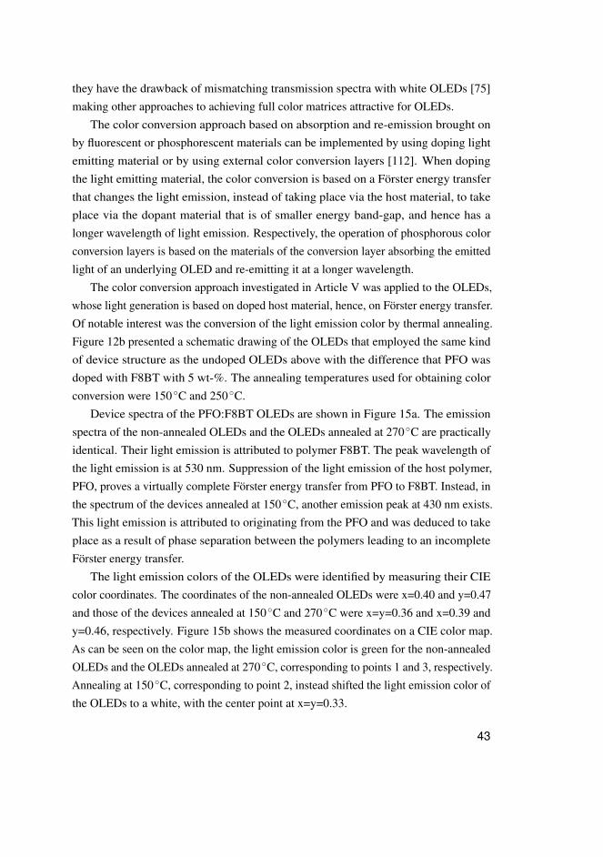
The color conversion approach investigated in Article V was applied to the OLEDs,whose light generation is based on doped host material, hence, on Förster energy transfer.Of notable interest was the conversion of the light emission color by thermal annealing.Figure 12b presented a schematic drawing of the OLEDs that employed the same kindof device structure as the undoped OLEDs above with the difference that PFO wasdoped with F8BT with 5 wt-%. The annealing temperatures used for obtaining colorconversion were 150◦C and 250◦C.
Device spectra of the PFO:F8BT OLEDs are shown in Figure 15a. The emissionspectra of the non-annealed OLEDs and the OLEDs annealed at 270 ◦C are practicallyidentical. Their light emission is attributed to polymer F8BT. The peak wavelength ofthe light emission is at 530 nm. Suppression of the light emission of the host polymer,PFO, proves a virtually complete Förster energy transfer from PFO to F8BT. Instead, inthe spectrum of the devices annealed at 150 ◦C, another emission peak at 430 nm exists.This light emission is attributed to originating from the PFO and was deduced to takeplace as a result of phase separation between the polymers leading to an incompleteFörster energy transfer.
The light emission colors of the OLEDs were identified by measuring their CIEcolor coordinates. The coordinates of the non-annealed OLEDs were x=0.40 and y=0.47and those of the devices annealed at 150◦C and 270 ◦C were x=y=0.36 and x=0.39 andy=0.46, respectively. Figure 15b shows the measured coordinates on a CIE color map.As can be seen on the color map, the light emission color is green for the non-annealedOLEDs and the OLEDs annealed at 270 ◦C, corresponding to points 1 and 3, respectively.Annealing at 150 ◦C, corresponding to point 2, instead shifted the light emission color ofthe OLEDs to a white, with the center point at x=y=0.33.
43

(a) (b)
Fig. 15. (a) Spectra of the F8BT:PFO-OLEDs. The devices were either non-annealed or an-nealed at 150 ◦C or 270 ◦C. (b) CIE chromaticity diagram (1931) giving color coordinates forthe respective devices: non-annealed OLEDs (point 1) and the OLEDs annealed at 150 ◦C(point 2) or 270 ◦C (point 3).
Luminance-voltage graphs for the PFO:F8BT OLEDs are presented in Figure 16. Themaximum luminance of the non-annealed devices measured at 13 V was 3000 cd/m2.The maximal current efficiency was 3 cd/A and the turn-on voltage was 6.3 V (deter-mined as the voltage required for reaching luminescence level of 10 cd/m2). With thesevalues, the non-annealed devices showed the best performance of the doped OLEDs. Thedevices annealed at 150 ◦C presented a luminance of 900 cd/m2 at 13 V, with a turn-onvoltage of 7.8 V and a current efficiency below 1 cd/A. Although optimization of deviceperformance was outside of the scope of the work, hence, better device performance wasexpected to be well achievable, it was notified in the work that the luminance level of theOLEDs annealed at 150◦C is already enough for many display applications [113, 114].
The performance of the devices annealed at the highest temperature, 270◦C, droppedsignificantly similarly to the non-doped PFO-OLEDs. Still, due to the doping theirluminance level was clearly higher than for corresponding non-doped devices andreached 400 cd/m2 at a voltage of 18 V. The turn-on voltage was raised to 12.6 V andthe current efficiency dropped to below 1 cd/A with the maximum value measured at18 V.
44
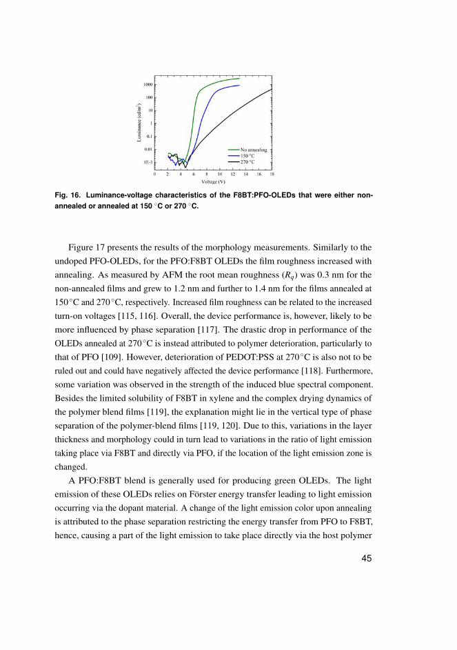
Fig. 16. Luminance-voltage characteristics of the F8BT:PFO-OLEDs that were either non-annealed or annealed at 150 ◦C or 270 ◦C.
Figure 17 presents the results of the morphology measurements. Similarly to theundoped PFO-OLEDs, for the PFO:F8BT OLEDs the film roughness increased withannealing. As measured by AFM the root mean roughness (Rq) was 0.3 nm for thenon-annealed films and grew to 1.2 nm and further to 1.4 nm for the films annealed at150◦C and 270 ◦C, respectively. Increased film roughness can be related to the increasedturn-on voltages [115, 116]. Overall, the device performance is, however, likely to bemore influenced by phase separation [117]. The drastic drop in performance of theOLEDs annealed at 270 ◦C is instead attributed to polymer deterioration, particularly tothat of PFO [109]. However, deterioration of PEDOT:PSS at 270 ◦C is also not to beruled out and could have negatively affected the device performance [118]. Furthermore,some variation was observed in the strength of the induced blue spectral component.Besides the limited solubility of F8BT in xylene and the complex drying dynamics ofthe polymer blend films [119], the explanation might lie in the vertical type of phaseseparation of the polymer-blend films [119, 120]. Due to this, variations in the layerthickness and morphology could in turn lead to variations in the ratio of light emissiontaking place via F8BT and directly via PFO, if the location of the light emission zone ischanged.
A PFO:F8BT blend is generally used for producing green OLEDs. The lightemission of these OLEDs relies on Förster energy transfer leading to light emissionoccurring via the dopant material. A change of the light emission color upon annealingis attributed to the phase separation restricting the energy transfer from PFO to F8BT,hence, causing a part of the light emission to take place directly via the host polymer
45

Fig. 17. Morphology of PFO:F8BT films that were spin-coated on top of a PE-DOT:PSS/ITO/glass stack. The upper row shows the morphology of the non-annealed film,and the middle and bottom rows show the morphology for the films annealed at 150 ◦C and270 ◦C, respectively. The left and middle columns present color maps of the film morphol-ogy data and roughness profiles, obtained with an optical profilometer, and the column onthe right shows 3D maps of the film morphology obtained with an AFM.
PFO. The performed annealing resulted in the color conversion of the OLEDs fromgreen to white, thereby showing that thermal annealing is an effective method for tuningthe light emission color of OLEDs made of this type of a blend. It is noteworthy that byfurther optimization color conversion from green to blue might also be possible. Thisis on the grounds that a doping concentration of 1 wt-% of F8BT to PFO should besufficient for reaching fully F8BT based light emission [121]. Therefore by reducingthe doping concentration, color conversion to blue might be realizable. The presentedmethod of color conversion could be applied to the fabrication of multicolor lightemitting devices or pixel matrices. If the color change is targeted in precise areas, pixels
46

or other shapes with a light emission color differing from the surrounding OLED areascould be created.
In addition, if a vertical type of separation, generally occurring in the blend-type ofpolymer films [119, 120], can be controlled by thermal annealing, it would also open upexciting possibilities for the fabrication of OLETs with additive color mixing or evenselective multicolor light emission: if the location of the light emission zone could betransferred in the vertical direction from a dopant rich film segment to a segment withreduced dopant, OLETs with voltage controlled light emission color could be realized.For this, vertical OLETs might offer a more suitable platform than horizontal types ofOLETs.
47

48

4 Discussion and conclusion
This thesis presented three types of color tuning techniques for organic light emittingdevices. Voltage controllable, two-color light emission, was demonstrated on OLETs.For OLEDs, color tuning was performed to enhance color purity and to convert the lightemission color permanently.
Two-color light emission was investigated on OLETs based on a three-layer het-erostructure device configuration that has been shown to be capable of high efficiencylight emission [41]. The multilayered structure represents one of the advantages oforganic electronic materials and their deposition methods. It has potential for tailoringdevice properties, and in this thesis two color light emission was investigated. Voltageswitchable light emission in red and green color, was demonstrated in Article III.
It was proposed that by further development of the device structure, it might bepossible to gain three-color light emission using a three-layer device structure. Thiscould be done by sandwiching the light emission layer with segmented doping in themiddle of the charge transport layers, so that it would create light emissions in all threeRGB-colors. Alternatively, charge transfer layers could also be used for producing lightemission in differing colors from the color of the main light emission layer. This wouldbe similar to the demonstration of two color light emission in Article III, where greenemission took place from the electron transport layer, while the main light emissionlayer produced red light.
A three-layer device structure gives versatility, but on the other hand, as wasconcluded in Article II, the sophisticated structure sets high requirements for thefabrication process. For multilayer structures, solution processing is challenging and thechoice of materials is virtually limited to materials that can be thermally evaporated,i.e. mainly to small molecules. In addition, the horizontal device structure adds tothe challenge. The long distance needed for charge carriers to travel, sets high qualityrequirements for layer morphology. This, in turn, further limits the choice of fabricationtechniques and materials. An applicable option for simplifying the fabrication processfor multilayer OLETs would be the use of a vertical type of device structure instead ofthe horizontal one. As the charge transfer in vertical OLETs takes place not along butthrough the layers, as in OLEDs, the distances of the charges to be transferred woulddecrease and prerequisites for the interface morphologies of the layers would not be that
49

demanding. Additionally, accurate alignment of the source and drain electrodes to formthe device channel would then not be required, which would enhance the possibility forroll-to-roll to fabrication.
The color tuning of OLEDs was investigated in two types of devices; undoped anddoped. The undoped OLEDs were made as blue light emitting, with polyfluorene PFOforming the light emission layer. Polyfluorenes are a widely used type of polymer inOLEDs, and blue light emitting polymers in general are of special importance sincethey can be doped to gain light emission in other colors. Blue polyfluorenes, however,generally suffer from undesired wide band emission caused by keto-defects shiftingtheir light emission color unintentionally towards green. In Article IV it was shown thatthis type of green emission could be removed by applying thermal annealing, althoughthermal annealing has often earlier been related to an increase of unwanted green lightemission. Significantly, also the performance of the OLEDs, with increased luminanceand current efficiency, was improved as a result of thermal treatment. Therefore, thermalannealing was seen as a potential method for tailoring the performance of blue lightemitting polyfluorene OLEDs.
The other type of OLEDs investigated, doped OLEDs, had a light emission layermade of PFO:F8BT. It was presented in Article V that a color conversion of this kind ofblend type polymer-OLEDs could be induced by thermal annealing. The conversion wasattributed to phase separation between the polymers and changed the light emissioncolor from the originally green light emission to a white light emission. The colorconversion was produced on OLEDs with a 5 wt-% doping concentration of F8BT toPFO. However, a doping concentration of 1 wt-% is already predicted to be enough forgaining full suppression of PFO emission [121], hence for producing green light fromnon-treated OLEDs. Thereby, converting the light emission color from green to bluemight be possible, if the doping concentration is decreased.
Further, in this thesis thermal annealing was the method used for inducing the colorconversion. However, presuming phase separation as the conversion mechanism, themethod could also be another type of treatment capable of producing polymer phaseseparation. This kind of a treatment could for instance be light radiation that turns intoheat, when hitting a device, or a solvent treatment produced by inkjet printing [122].
Utilizing phase separation, produced by thermal annealing or the other proposedmethods, advantageously for achieving color conversion of OLEDs is proposed as aprospective method to ease the fabrication of multicolor light emitting pixel matrices. Inthis case, pixel matrices could be fabricated from a single light emission layer: targeted
50

areas would be treated to achieve phase separation, and hence, light emission in adifferent color than the surrounding untreated areas of the OLED. Especially, large areadisplay applications might be of interest, because the imprecision in the outlines of thearea of the induced phase separation would not be that critical.
It would also be interesting to look at exploiting vertical type of phase separationgenerally occurring in blend polymers layers [119, 120] for the fabrication of voltagetunable multicolor light emitting devices. This would be of special interest for OLETs,where the location of the light emission zone can be controlled. In this way the color ofthe light emission could be tuned by moving the location of the light emission zonefrom a region with minimum phase separation, to the region representing maximaldegree of phase separation. It might be possible to utilize horizontal OLETs for this.However, vertical types of OLETs might be a more feasible candidate for the purposebecause the location of the light emission would move with biasing conditions in avertical direction, not spatially as is the case with the movement primarily taking placein horizontal ambipolar OLETs.
To conclude the thesis, much research work has this far been done on bridging thegap in the performance of the organic semiconductors and inorganic semiconductorsand on producing device features similar to those known in inorganic electronics.Instead, maybe less effort has been directed toward research into exploiting the inherentproperties of organic materials advantageously. This thesis intended to do this to promotecolor tuning features which would be an advantageous feature of organic light emittingdevices not yet exploited to its full extent.
51

52

References
1. Mobile phones and smartphones with OLED screens. OLED-info. Referred on April 14th,2015. URI: http://www.oled-info.com/oled_devices/mobile_phones.
2. Nexus - 6 Enemmän tilaa katsella. Google. Referred on April 14th, 2015. URI:http://www.google.com/nexus/6/.
3. LG OLED TV - What is OLED? LG Electronics. Referred on April 14th, 2015. URI:http://www.lg.com/us/experience-tvs/oled-tv/what-is-oled-tv.jsp.
4. Samsung’s Nano Crystal Technology vs. Quantum Dot. LCDTV Buying Guide. Referred onJanuary 21th, 2016. URI: http://lcdtvbuyingguide.com/hdtv/nano-crystal-vs-quantum-dot.html.
5. Think you’ve seen colour? Think again. Samsung. Referred on January 21th, 2016. URI:http://www.samsung.com/uk/discover/tv/think-youve-seen-colour-think-again/.
6. OLED vs LED: There’s just no comparison. TechHive. Referred on May 23rd,2016. URI: http://www.techhive.com/article/3018446/smart-tv/oled-vs-led-theres-just-no-comparison.html.
7. Chen S, Deng L, Xie J, Peng L, Xie L, Fan Q & Huang W (2010) Recent developments intop-emitting organic light-emitting diodes. Advanced Materials 22: 5227–5239.
8. McCarthy MA, Liu B, Donoghue EP, Kravchenko I, Kim DY, So F & Rinzler AG (2011)Low-voltage, low-power, organic light-emitting transistors for active matrix displays.Science 232: 570–573.
9. Review of the LG Electronics 77EG9900 77-Inch 4k Ultra HD 3D Flexible CurvedOLED TV. 4k. Referred on January 21th, 2016. URI: http://4k.com/tv/a-review-of-the-lg-electronics-77eg9900-77-inch-4k-ultra-hd-3d-flexible-curved-oled-tv/.
10. Facchetti A (2011) π-conjugated polymers for organic electronics and photovoltaic cellapplications. Chemistry of Materials 23: 733–758.
11. Shaheen SE, Ginley DS & Jabbour GE (2005) Organic-based photovoltaics: toward low-costpower generation. MRS Bulletin 30: 10–19.
12. Kim MG, Kanatzidis MG, Facchetti A & Marks TJ (2011) Low-temperature fabrication ofhigh-performance metal oxide thin-film electronics via combustion processing. NatureMaterials 10: 382–388.
13. Sekitani T & Someya T (2010) Stretchable, large-area organic electronics. AdvancedMaterials 22: 2228–2246.
14. Chiang CK, Fincher Jr CR, Park YW, Heeger AJ, Shirakawa H, Louis EJ, Gau SC &MacDiarmid AG (1977) Electrical conductivity in doped polacetylene. Physical ReviewLetters 39: 1098–1101.
15. Heeger AJ (2001) Semiconducting and metallic polymers: the fourth generation of polymericmaterials (Nobel lecture). Angewandte Chemie International Edition 40: 2591–2611.
16. MacDiarmid AG (2001) ”Synthetic Metals”: a novel role for organic polymers (Nobellecture). Angewandte Chemie International Edition 40: 2581–2590.
17. Shirakawa H (2000) The discovery of polyacetylene film: the dawning of an era ofconducting polymers (Nobel lecture). Angewandte Chemie International Edition 40:2574–2580.
53

18. Bao Z & Locklin J (eds.) (2007) Organic field-effect transistors. CRC Press, Taylor &Francis Group, Boca Raton.
19. Bernius MT, Inbasekaran M, O’Brien J & Wu W (2000) Progress with light-emittingpolymers. Advanced Materials 12: 1737–1750.
20. Forrest SR (2004) The path to ubiquitous and low-cost organic electronic appliances onplastic. Nature 428: 911–918.
21. Irimia-Vladu M, Sariciftci NS & Bauer S (2011) Exotic materials for bio-organic electronics.Journal of Materials Chemistry 21: 1350–1361.
22. Progress with printed electronics. IDTechEx. Referred on April 18th, 2015. URI:http://www.idtechex.com/journal/print-articles.asp?articleids=6796.
23. OLED technology: introduction and basics. OLED-info. Referred on April 15th, 2015. URI:http://www.oled-info.com/oled-technology.
24. De Mello J, Anthony J & Lee S (2015) Organic Electronics: Recent Developments.ChemPhysChem 16: 1099–1100.
25. Tang CW & VanSlyke SA (1987) Organic electroluminescent diodes. Applied PhysicsLetters 51: 913–915.
26. Cao Y, Yu G, Zhang C, Menon R & Heeger AJ (1997) Polymer light-emitting diodes withpolyethylene dioxythiophene–polystyrene sulfonate as the transparent anode. SyntheticMetals 87: 171–174.
27. Roman LS, Berggren M & Inganäs O (1999) Polymer diodes with high rectification. AppliedPhysics Letters 75: 3557–3559.
28. Elschner A, Bruder F, Heuer HW, Jonas F, Karbach A, Kirchmeyer S, Thurm S & WehrmannR (2000) PEDT/PSS for efficient hole-injection in hybrid organic light-emitting diodes.Synthetic Metals 111-112: 139–143.
29. Kalyani NT & Dhoble S (2012) Organic light emitting diodes: energy saving lightingtechnology–a review. Renewable and Sustainable Energy Reviews 16: 2696–2723.
30. Geffroy B, le Roy P & Prat C (2006) Organic light-emitting diode (OLED) technology:materials, devices and display technologies. Polymer International 55: 572–582.
31. Shoustikov AA & Thompson ME (1998) Electroluminescence color tuning by dye dopingin organic light-emitting diodes. IEEE Journal of Selected Topics in Quantum Electronics 4:3–13.
32. Sharpe LT, Stockman A, Jagla W & Jägle H (2005) A luminous efficiency function, V*(λ ),for daylight adaptation. Journal of Vision 5: 948–68.
33. Schanda J (ed.) (2007) Colorimetry: Understanding the CIE System. WILEY, New Yersey.34. Hepp A, Heil H, Weise W, Ahles M, Schmechel R & von Seggern H (2003) Light-emitting
field-effect transistor based on a tetracene thin film. Physical Review Letters 91: 1–4.35. Muccini M (2006) Progress article: A bright future for organic field-effect transistors.
Nature Materials 5: 605–613.36. Tessler N, Pinner DJ, Cleave V, Ho PKH, Friend RH, Yahioglu G, Le Barny P, Gray J,
de Souza M & Rumbles G (2000) Properties of light emitting organic materials within thecontext of future electrically pumped lasers. Synthetic Metals 115: 57–62.
37. Baldo M, Holmes R & Forrest S (2002) Prospects for electrically pumped organic lasers.Physical Review B 66: 035321.
38. Cicoira F & Santato C (2007) Organic Light Emitting Field Effect Transistors: Advancesand Perspectives. Advanced Functional Materials 17: 3421–3434.
54

39. Zaumseil J, Friend RH & Sirringhaus H (2006) Spatial control of the recombination zone inan ambipolar light-emitting organic transistor. Nature Materials 5: 69–74.
40. Zaumseil J, McNeill CR, Bird M, Smith DL, Paul Ruden P, Roberts M, McKiernan MJ,Friend RH & Sirringhaus H (2008) Quantum efficiency of ambipolar light-emitting polymerfield-effect transistors. Journal of Applied Physics 103(6): 064517.
41. Capelli R, Toffanin S, Generali G, Usta H, Facchetti A & Muccini M (2010) Organiclight-emitting transistors with an efficiency that outperforms the equivalent light-emittingdiodes. Nature Materials 9: 496–503.
42. Hsu BBY, Duan C, Namdas EB, Gutacker A, Yuen JD, Huang F, Cao Y, Bazan GC, SamuelIDW & Heeger AJ (2012) Control of efficiency, brightness, and recombination zone inlight-emitting field effect transistors. Advanced Materials 24: 1171–1175.
43. Schidleja M, Melzer C, Roth M, Schwalm T, Gawrisch C, Rehahn M & Von Seggern H(2014) The impact of contact formation on the light emission from ambipolar transistors.Applied Physics Letters 113303: 14–17.
44. Feldmeier EJ, Schidleja M, Melzer C & von Seggern H (2010) A color-tuneable organiclight-emitting transistor. Advanced Materials 22: 3568–72.
45. Swensen JS, Soci C & Heeger AJ (2005) Light emission from an ambipolar semiconductingpolymer field-effect transistor. Applied Physics Letters 87: 253511.
46. Swensen JS, Yuen J, Gargas D, Buratto SK & Heeger AJ (2007) Light emission from anambipolar semiconducting polymer field effect transistor: analysis of the device physics.Journal of Applied Physics 102: 1–5.
47. Toffanin S, Capelli R, Koopman W, Generali G, Cavallini S, Stefani A, Saguatti D, Ruani G& Muccini M (2013) Organic light-emitting transistors with voltage-tunable lit area and fullchannel illumination. Laser and Photonics Reviews 7: 1011–1019.
48. Verlaak S, Cheyns D, Debucquoy M, Arkhipov V & Heremans P (2004) Numericalsimulation of tetracene light-emitting transistors: a detailed balance of exciton processes.Applied Physics Letters 85: 2405.
49. Zaumseil J, Donley CL, Kim JS, Friend RH & Sirringhaus H (2006) Efficient top-gate,ambipolar, light-emitting field-effect transistors based on a green-light-emitting polyfluorene.Advanced Materials 18: 2708–2712.
50. Gwinner MC, Kabra D, Roberts M, Brenner TJK, Wallikewitz BH, McNeill CR, Friend RH& Sirringhaus H (2012) Highly efficient single-layer polymer ambipolar light-emittingfield-effect transistors. Advanced Materials 24: 2728–34.
51. Rost C, Karg S, Riess W, Loi MA, Murgia M & Muccini M (2004) Ambipolar light-emittingorganic field-effect transistor. Applied Physics Letters 85: 1613.
52. Loi MA, Rost-Bietsch C, Murgia M, Karg S, Riess W & Muccini M (2006) Tuningoptoelectronic properties of ambipolar organic light-emitting transistors using a bulk-heterojunction approach. Advanced Functional Materials 16: 41–47.
53. Szendrei K, Jarzab D, Chen Z, Facchetti A & Loi MA (2010) Ambipolar all-polymer bulkheterojunction field-effect transistors. Journal of Materials Chemistry 20: 1317.
54. Rost C, Karg S, Riess W, Loi M, Murgia M & Muccini M (2004) Light-emitting ambipolarorganic heterostructure field-effect transistor. Synthetic Metals 146: 237–241.
55. Dinelli F, Capelli R, Loi MA, Murgia M, Muccini M, Facchetti A & Marks TJ (2006)High-mobility ambipolar transport in organic light-emitting transistors. Advanced Materials18: 1416–1420.
55

56. Sandberg HGO, Bäcklund TG, Österbacka R & Stubb H (2004) High-Performance All-Polymer Transistor Utilizing a Hygroscopic Insulator. Advanced Materials 16(13): 1112–1115.
57. Panzer MJ & Frisbie CD (2005) Polymer electrolyte gate dielectric reveals finite windowsof high conductivity in organic thin film transistors at high charge carrier densities. Journalof the American Chemical Society 127(19): 6960–1.
58. Herlogsson L, Crispin X, Robinson ND, Sandberg M, Hagel OJ, Gustafsson G & BerggrenM (2007) Low-Voltage Polymer Field-Effect Transistors Gated via a Proton Conductor.Advanced Materials 19(1): 97–101.
59. Larsson O, Said E, Berggren M & Crispin X (2009) Insulator Polarization Mechanisms inPolyelectrolyte-Gated Organic Field-Effect Transistors. Advanced Functional Materials19(20): 3334–3341.
60. Cho JH, Lee J, Xia Y, Kim B, He Y, Renn MJ, Lodge TP & Frisbie CD (2008) Printableion-gel gate dielectrics for low-voltage polymer thin-film transistors on plastic. Naturematerials 7(11): 900–906.
61. Xia Y, Zhang W, Ha M, Cho JH, Renn MJ, Kim CH & Frisbie CD (2010) Printed sub-2 VGel-electrolyte-gated polymer transistors and circuits. Advanced Functional Materials20(4): 587–594.
62. Kim SH, Hong K, Xie W, Lee KH, Zhang S, Lodge TP & Frisbie CD (2013) Electrolyte-gatedtransistors for organic and printed electronics. Advanced Materials 25(13): 1822–1846.
63. Chua LL, Zaumseil J, Chang JF & Ou ECW (2005) General observation of n-type field-effectbehaviour in organic semiconductors. Nature 434: 194–199.
64. Dimitrakopoulos CD & Malenfant PRL (2002) Organic thin film transistors for large areaelectronics. Advanced Materials 14: 99–117.
65. Berggren M, Inganäs O, Gustafsson G, Rasmusson J, Andersson MR, Hjertberg T &Wennerström O (1994) Light-emitting diodes with variable colours from polymer blends.Nature 372: 444–446.
66. Berggren M, Inganäs O, Gustafsson G, Andersson MR, Hjertberg T & Wennerström O(1995) Controlling colour by voltage in polymer light emitting diodes. Synthetic Metals 71:2185–2186.
67. Granström M & Inganäs O (1996) White light emission from a polymer blend light emittingdiode. Applied Physics Letters 68: 147.
68. Tasch S, Niko A, Leising G & Scherf U (1996) Highly efficient electroluminescence of newwide band gap ladder-type poly(para-phenylenes). Applied Physics Letters 68: 1090.
69. Reyes R, Cremona M, Teotonio EE, Brito HF & Malta OL (2004) Voltage color tunableOLED with (Sm,Eu)-β -diketonate complex blend. Chemical Physics Letters 396: 54–58.
70. Yoshida M, Fujii A, Ohmori Y & Yoshino K (1996) Three-layered multicolor organicelectroluminescent device. Applied Physics Letters 69: 734.
71. Hamaguchi M & Yoshino K (1996) Color-variable electroluminescence from multilayerpolymer films. Applied Physics Letters 69: 143.
72. Burrows PE, Gu G, Bulovic V, Shen Z, Forrest SR & Thompson ME (1997) Achieving full-color organic light-emitting devices for lightweight, flat-panel displays. IEEE Transactionson Electron Devices 44: 1188–1203.
73. Lu YJ, Chang CH, Lin CL, Wu CC, Hsu HL, Chen LJ, Lin YT & Nishikawa R (2008)Achieving three-peak white organic light-emitting devices using wavelength-selective mirrorelectrodes. Applied Physics Letters 92: 1–4.
56

74. Xiong Y, Xu W, Li C, Liang B, Zhao L, Peng J, Cao Y & Wang J (2008) Utilizing whiteOLED for full color reproduction in flat panel display. Organic Electronics 9: 533–538.
75. Chang CH, Cheng HC, Lu YJ, Tien KC, Lin HW, Lin CL, Yang CJ & Wu CC (2010)Enhancing color gamut of white OLED displays by using microcavity green pixels. OrganicElectronics 11: 247–254.
76. Tasch S, Brandstätter C, Meghdadi F, Leising G, Froyer G & Athouel L (1997) Red-green-blue light emission from a thin film electroluminescence device based on parahexaphenyl.Advanced Materials 9: 33–36.
77. Swanson SA, Wallraff GM, Chen JP, Zhang W, Bozano LD, Carter KR, Salem JR, Villa R &Scott JC (2003) Stable and efficient fluorescent red and green dyes for external and internalconversion of blue OLED emission. Chemistry of Materials 15: 2305–2312.
78. Wu CC, Sturm JC, Register Ra & Thompson ME (1996) Integrated three-color organiclight-emitting devices. Applied Physics Letters 69: 3117.
79. Kubota H, Miyaguchi S, Ishizuka S, Wakimoto T, Funaki J, Fukuda Y, Watanabe T, Ochi H,Sakamoto T, Miyake T, Tsuchida M, Ohshita I & Tohma T (2000) Organic LED full colorpassive-matrix display. Journal of Luminescence 87: 56–60.
80. Burrows PE, Forrest SR, Sibley SP & Thompson ME (1996) Color-tunable organic light-emitting devices. Applied Physics Letters 69: 2959.
81. Shen Z, Burrows PE & Bulovic V (1997) Three-color, tunable, organic light-emittingdevices. Science 276: 2009–2011.
82. Forrest SR, Burrows PE, Shen Z, Gu G, Bulovic V & Thompson ME (1997) The stackedOLED (SOLED): a new type of organic device for achieving high-resolution full-colordisplays. Synthetic Metals 91: 9–13.
83. Cherpak V, Gassmann A, Stakhira P, Volyniuk D, Grazulevicius JV, Michaleviciute A,Tomkeviciene A, Barylo G & Von Seggern H (2014) Three-terminal light-emitting devicewith adjustable emission color. Organic Electronics 15(7): 1396–1400.
84. Ke TH, Gehlhaar R, Chen CH, Lin JT, Wu CC & Adachi C (2009) High efficiency bluelight emitting unipolar transistor incorporating multifunctional electrodes. Applied PhysicsLetters 94: 153307.
85. Ke TH, Gehlhaar R, Chen CH, Lin JT, Wu CC & Adachi C (2009) Single molecule colorcontrollable light emitting organic field effect transistors for white light emission with highcolor stability. Applied Physics Letters 95: 063303.
86. Loi MA, da Como E, Dinelli F, Murgia M, Zamboni R, Biscarini F & Muccini M (2004)Supramolecular organization in ultra-thin films of α-sexithiophene on silicon dioxide.Nature Materials 4: 81–85.
87. Feldmeier EJ & Melzer C (2011) Multiple colour emission from an organic light-emittingtransistor. Organic Electronics 12: 1166–1169.
88. Melzer C & von Seggern H (2014) The color change in polychromatic organic light-emitting field-effect transistors: Optical filtering versus reemission. Organic Electronics 15:2505–2512.
89. Uddin A, Lee CB, Hu X, Wong TKS & Sun XW (2006) Effect of doping on optical andtransport properties of charge carriers in Alq3. Journal of Crystal Growth 288: 115–118.
90. Tang CW, VanSlyke SA & Chen CH (1989) Electroluminescence of doped organic thinfilms. Journal of Applied Physics 65: 3610.
57

91. Itano K, Ogawa H & Shirota Y (1998) Exciplex formation at the organic solid-stateinterface: yellow emission in organic light-emitting diodes using green-fluorescent tris(8-quinolinolato)aluminum and hole-transporting molecular materials with low ionizationpotentials. Applied Physics Letters 72: 636–638.
92. Liao SH, Shiu JR, Liu SW, Yeh SJ & Chen YH (2009) Hydroxynaphthyridine-derivedgroup III metal chelates: wide band gap and deep blue analogues of green Alq3 (tris(8-hydroxyquinolate)aluminum) and their versatile applications for organic light-emittingdiodes. Journal of the American Chemical Society 131: 763–777.
93. Craig MR, de Kok MM, Hofstraat JW, Schenning APHJ & Meijer EW (2003) Improvingcolor purity and stability in a blue emitting polyfluorene by monomer purification. Journalof Materials Chemistry 13: 2861.
94. Peng Q, Xu J, Li M & Zheng W (2009) Blue emitting polyfluorenes containing dendronizedcarbazole and oxadiazole pendants: synthesis, optical properties, and electroluminescentproperties. Macromolecules 42: 5478–5485.
95. Ying L, Zou J, Yang W, Zhang A, Wu Z, Zhao W & Cao Y (2009) Novel, blue light-emittingpolyfluorenes containing a fluorinated quinoxaline unit. Dyes and Pigments 82: 251–257.
96. Zhao Q, Liu SJ & Huang W (2009) Polyfluorene-based blue-emitting materials. Macro-molecular Chemistry and Physics 210: 1580–1590.
97. Bliznyuk VN, Carter SA, Scott JC, Kla G, Miller RD & Miller DC (1999) Electricaland photoinduced degradation of polyfluorene based films and light-emitting devices.Macromolecules 32: 361–369.
98. List EJW, Guentner R, Scanducci de Freitas P & Scherf U (2002) The effect of keto defectsites on the emission properties of polyfluorene-type materials. Advanced Materials 14: 374.
99. Lupton JM, Craig MR & Meijer EW (2002) On-chain defect emission in electroluminescentpolyfluorenes. Applied Physics Letters 80: 4489.
100. Sainova D, Neher D, Dobruchowska E, Luszczynska B, Glowacki I, Ulanski J, Nothofer HG& Scherf U (2003) Thermoluminescence and electroluminescence of annealed polyfluorenelayers. Chemical Physics Letters 371: 15–22.
101. Romaner L, Pogantsch A, Scandiucci de Freitas P, Scherf U, Gaal M, Zojer E & List EJW(2003) The origin of green emission in polyfluorene-based conjugated polymers: on-chaindefect fluorescence. Advanced Functional Materials 13: 597–601.
102. Kreyenschmidt M, Klaerner G, Fuhrer T, Ashenhurst J, Karg S, Chen WD, Lee VY, Scott JC& Miller RD (1998) Thermally stable blue-light-emitting copolymers of poly(alkylfluorene).Macromolecules 31: 1099–1103.
103. Lee JIL, Lee VYL & Miller RD (2002) Excimer and aggregate formations in poly(fluorene)s.ETRI Journal 24: 409–414.
104. Wu Y, Hu B & Howe J (2005) Morphology-dependent exciton emission and energy transferin fluorene-polymer-related fluorescent and phosphorescent composite films spin cast from amixture of two dissimilar organic solvents. Journal of Applied Physics 98: 103510.
105. Kreouzis T, Poplavskyy D, Tuladhar S, Campoy-Quiles M, Nelson J, Campbell A & BradleyD (2006) Temperature and field dependence of hole mobility in poly(9,9-dioctylfluorene).Physical Review B 73: 1–15.
106. Grell M, Bradley DDC, Long X, Chamberlain T, Inbasekaran M, Woo EP & Soliman M(1998) Chain geometry, solution aggregation and enhanced dichroism in the liquidcrystallineconjugated polymer poly(9,9-dioctylfluorene). Acta Polymerica 49: 439–444.
58

107. Teetsov J & Fox MA (1999) Photophysical characterization of dilute solutions and orderedthin films of alkyl-substituted polyfluorenes. Journal of Materials Chemistry 9: 2117–2122.
108. Cadby A, Lane P, Mellor H, Martin S, Grell M, Giebeler C, Bradley D, Wohlgenannt M,An C & Vardeny Z (2000) Film morphology and photophysics of polyfluorene. PhysicalReview B 62: 15604–15609.
109. Scherf U & List E (2002) Semiconducting polyfluorenes–towards reliable structure-propertyrelationships. Advanced Materials 14: 477–487.
110. Khan ALT, Sreearunothai P, Herz LM, Banach MJ & Köhler A (2004) Morphology-dependent energy transfer within polyfluorene thin films. Physical Review B 69: 085201.
111. Ko CW & Tao YT (2001) Bright white organic light-emitting diode. Applied Physics Letters79: 4234.
112. Duggal AR, Shiang JJ, Heller CM & Foust DF (2002) Organic light-emitting devices forillumination quality white light. Applied Physics Letters 80: 3470–3472.
113. Popovic ZD & Aziz H (2002) Reliability and degradation of small molecule-based organiclight-emitting devices (OLEDs). IEEE Journal on Selected Topics in Quantum Electronics8: 362–371.
114. He G, Pfeiffer M, Leo K, Hofmann M, Birnstock J, Pudzich R & Salbeck J (2004) High-efficiency and low-voltage p-i-n electrophosphorescent organic light-emitting diodes withdouble-emission layers. Applied Physics Letters 85: 3911–3913.
115. Chen SF & Wang CW (2004) Influence of the hole injection layer on the luminescentperformance of organic light-emitting diodes. Applied Physics Letters 85: 765–767.
116. Singh R & Katiyar M (2010) Polysilane based ultraviolet light-emitting diodes withimproved turn-on voltage, stability and color purity. Synthetic Metals 160: 1892–1895.
117. Voigt M, Chappell J, Rowson T, Cadby A, Geoghegan M, Jones RAL & Lidzey DG (2005)The interplay between the optical and electronic properties of light-emitting-diode applicableconjugated polymer blends and their phase-separated morphology. Organic Electronics 6:35–45.
118. Friedel B, Keivanidis PE, Brenner TJK, Abrusci A, McNeill CR, Friend RH & GreenhamNC (2009) Effects of layer thickness and annealing of PEDOT:PSS layers in organicphotodetectors. Macromolecules 42: 6741–6747.
119. Kim JS, Ho PKH, Murphy CE & Friend RH (2004) Phase aeparation in polyfluorene-basedconjugated polymer blends: lateral and vertical analysis of blend spin-cast thin films.Macromolecules 37: 2861–2871.
120. Xia Y & Friend RH (2006) Phase separation of polyfluorene-based blend films and itsinfluence on device operations. Advanced Materials 18: 1371–1376.
121. Morgado J, Moons E, Friend RH & Cacialli F (2001) De-mixing of polyfluorene-basedblends by contact with acetone: electro- and photo-luminescence probes. AdvancedMaterials 13: 810–814.
122. Yoshioka Y & Jabbour GE (2006) Desktop inkjet printer as a tool to print conductingpolymers. Synthetic Metals 156(11-13): 779–783.
59

60

Original publications
I Jokinen K, Popov A, Lappalainen J, Sliz R, Fabritius T, Kordas K, Myllylä R and Vasiliev A(2016) Performance enhancement of polymer electrolyte MEIS hydrogen sensor by DC-biasing. IEEE Sensors Journal 16: 5292 – 5297.
II Jokinen K, Bykov A, Sliz R and Myllyla R (2012) Behaviour of electron and hole currentsin a 3-layer heterostructure OLET. Proc. SPIE 8435, Organic Photonics V: 84351L.
III Jokinen K, Bykov A, Fabritius T and Myllylä R (2014) Two-color emission in three-layerheterostructure OLETs. Proc. SPIE 9183, Organic Light Emitting Materials and DevicesXVIII: 91831Q.
IV Jokinen K, Bykov A, Sliz R, Remes K, Fabritius T and Myllylä R (2015). Luminescenceand spectrum variations caused by thermal annealing in undoped and doped polyfluoreneOLEDs. Solid-State Electronics 103: 184 – 189.
V Jokinen K, Bykov AV, Sliz R, Remes K, Fabritius T and Myllylä R (2015) Light emissioncolor conversion of polyfluorene-blend OLEDs induced by thermal annealing. IEEETransactions on Electron Devices 62: 2238 – 2243.
Reprinted with permission from IEEE (I,V), SPIE (II,III) and Elsevier (IV).
Original publications are not included in the electronic version of the thesis.
61

62

A C T A U N I V E R S I T A T I S O U L U E N S I S
Book orders:Granum: Virtual book storehttp://granum.uta.fi/granum/
S E R I E S C T E C H N I C A
600. Mustamo, Pirkko (2017) Greenhouse gas fluxes from drained peat soils : acomparison of different land use types and hydrological site characteristics
601. Upola, Heikki (2017) Disintegration of packaging material : an experimental studyof approaches to lower energy consumption
602. Eskelinen, Riku (2017) Runoff generation and load estimation in drained peatlandareas
603. Kokkoniemi, Joonas (2017) Nanoscale sensor networks : the THz band as acommunication channel
604. Luoto, Petri (2017) Co-primary multi-operator resource sharing for small cellnetworks
605. Yrjölä, Seppo (2017) Analysis of technology and business antecedents forspectrum sharing in mobile broadband networks
606. Suikkanen, Essi (2017) Detection algorithms and ASIC designs for MIMO–OFDMdownlink receivers
607. Niemelä, Ville (2017) Evaluations and analysis of IR-UWB receivers for personalmedical communications
608. Keränen, Anni (2017) Water treatment by quaternized lignocellulose
609. Jutila, Mirjami (2017) Adaptive traffic management in heterogeneouscommunication networks
610. Shahmarichatghieh, Marzieh (2017) Product development sourcing strategies overtechnology life cycle in high-tech industry
611. Ylitalo, Pekka (2017) Value creation metrics in systematic idea generation
612. Hietajärvi, Anna-Maija (2017) Capabilities for managing project alliances
613. Kangas, Maria (2017) Stability analysis of new paradigms in wireless networks
614. Roivainen, Antti (2017) Three-dimensional geometry-based radio channel model :parametrization and validation at 10 GHz
615. Chen, Mei-Yu (2017) Ultra-low sintering temperature glass ceramic compositionsbased on bismuth-zinc borosilicate glass
616. Yliniemi, Juho (2017) Alkali activation-granulation of fluidized bed combustion flyashes
617. Iljana, Mikko (2017) Iron ore pellet properties under simulated blast furnaceconditions : Investigation on reducibility, swelling and softening
C618etukansi.kesken.fm Page 2 Tuesday, May 16, 2017 8:58 AM

UNIVERSITY OF OULU P .O. Box 8000 F I -90014 UNIVERSITY OF OULU FINLAND
A C T A U N I V E R S I T A T I S O U L U E N S I S
University Lecturer Tuomo Glumoff
University Lecturer Santeri Palviainen
Postdoctoral research fellow Sanna Taskila
Professor Olli Vuolteenaho
University Lecturer Veli-Matti Ulvinen
Planning Director Pertti Tikkanen
Professor Jari Juga
University Lecturer Anu Soikkeli
Professor Olli Vuolteenaho
Publications Editor Kirsti Nurkkala
ISBN 978-952-62-1588-4 (Paperback)ISBN 978-952-62-1589-1 (PDF)ISSN 0355-3213 (Print)ISSN 1796-2226 (Online)
U N I V E R S I TAT I S O U L U E N S I SACTAC
TECHNICA
U N I V E R S I TAT I S O U L U E N S I SACTAC
TECHNICA
OULU 2017
C 618
Karoliina Jokinen
COLOR TUNING OF ORGANIC LIGHT EMITTING DEVICES
UNIVERSITY OF OULU GRADUATE SCHOOL;UNIVERSITY OF OULU,FACULTY OF INFORMATION TECHNOLOGY AND ELECTRICAL ENGINEERING
C 618
AC
TAK
aroliina JokinenC618etukansi.kesken.fm Page 1 Tuesday, May 16, 2017 8:58 AM