Embed Size (px)
Citation preview

Technical Report No. 20-70-MET 9
BY
GORDON A. SARGENT
Department of Metallurgical Engineering
and Materials Science
https://ntrs.nasa.gov/search.jsp?R=19700019278 2020-03-12T02:04:30+00:00Z
COLLEGE OF ENGINEERING UNIVERSITY OF KENTUCKY
Robert M. Drake, Jr., Ph.D. Dean, College of Engineering and
Director, Office of Research and Engineering Ser%+ces
David K. Blythe, M.C.E. Associate Dean, Continuing ~ducatfon and Extension,
College of Engineering
James E. Funk, Ph.D. Associate Dean, Graduate Frograms, College of Engineering
Warren W. Walton, M.S. Assistant Dean, College of Engineering
Blaine F. Parker, Ph.D. Chairman, Department of Agricultural Engineering
Robert B. Grieves, Ph.D. Chairman, Department of Chemical Engineering
Staley F. Adams, Ph.D. Chairman, Department of Civil Engineering
Robert L. Cosgriff, Ph.D. Chairman, Department of Electrical Engineering
Oscar W. Dillon, D.Eng.Sci. Chairman, Department of Engineering Mechanics
Roger Eichhorn, Ph.D. Chairman, Department of Mechanical Engineering
Hans Conrad, D.Eng. Chairman, Department of Metallurgical Engineering
Russell E. Puckett, R4.S. Associate Director, Offioe of Research and
Engineering Services
RESEARCH STUDY OF STRUCTURAL DAMAGE
PRODUCED IN SILICON SEMICONDUCTORS
BY NEUTRON IRRADIATION
Semi-Annual Report
MAY 1970
GORDON A. SARGENT
Department of Metallurgical Engineering and Materials Science
This work was performed for the Jet Propulsion Laboratory,
California Institute of Technology (contract 952561), as sponsored
by the National Aeronautics and Space Administration under
Contract NAS7-100.
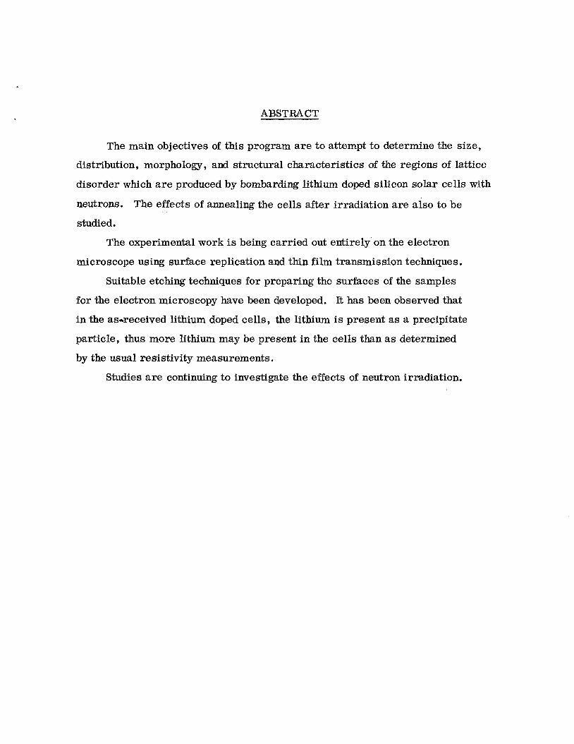
ABSTRACT
The main objectives of this program a r e to attempt to determine the size,
distribution, morphology, and structural characteristics of the regions of lattice
disorder which a re produced by bombarding lithium doped silicon solar cells with
neutrons. The effects of annealing the cells after irradiation are also to be
studied.
The experimental work is being carried out entirely on the electron
microscope using surface replication and thin film transmission techniques.
Suitable etching techniques for preparing the surfaces of the samples
for the electron microscopy have been developed. It has been observed that
in the as-received lithium doped cells, the lithium is present as a precipitate
particle, thus more lithium may be present in the cells than a s determined
by the usual resistivity measurements.
Studies a re continuing to investigate the effects of neutron irradiation.

CONTENTS
Page
Introduction ................................................. 1
Progress . . . . . . . . . . . . . . . . . . . . . . . . . . . . .es.o.e.. . . . .ee.. . . . . ... 5
Experimental Results ..................... ... ....... ... .. .... 11
C ~ n ~ l u ~ i o n s ................................................. 17
Plans for next reporting period ................................ 17
References ........................e.ee.e.....,.......... ... 18
FIGURES
............ 1 . Surface replica of undoped silicon solar cell X 15. 000 8
............... . 2 Schematic diagram of chemical polishing machine 10
3 . Surface replica of lithium doped (10' atoms/cm3) silicon solar
4 . Thin film transmission photograph of undoped silicon solar cell
X25. 000 .................................................... 12
5 . Thin film transmission photograph of lithium doped (loL7 atoms/cm3)
silicon solar cell X25. 000 ..................................... 14
6 . Electron diffraction pattern from thin film of undoped silicon solar
cell ...................................................... 14
......... 7 . (a) Interpretation of the diffraction pattern shown in Figure 6 15
........ 7 . (b) Interpretation of the diffraction pattern shown in Figure 8 15
8 . Electron diffraction pattern from thin film of lithium doped 17 3 (10 atoms/cm ) silicon solar cell ............................. 16
TABLES
I . Etchants for preparing the surface of silicon prior to replication . . 7
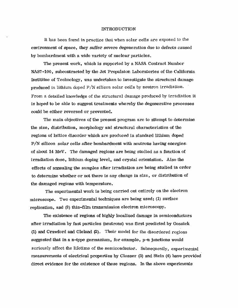
INTRODUCTION
It has been found in practice that when solar cells are exposed to the
environment of space, they suffer severe degeneration due to defects caused
by bombardment with a wide variety of nuclear particles.
The present work, which is supported by a NASA Contract Number
NAS7-100, subcontracted by the Jet Propulsion Laboratories of the California
Instititue of Technology, was undertaken to investigate the structural damage
produced in lithium doped P/N silicon solar cells by neutron irradiation.
From a detailed knowledge of the structural damage produced by irradiation it
is hoped to be able to suggest treatments whereby the degenerative processes
could be either reversed o r prevented.
The main objectives of the present program are to attempt to determine
the size, distribution, morphology and structural characteristics of the
regions of lattice disorder which are produced in standard lithium doped
P/N silicon solar cells after bombardment with neutrons having energies
of about 14 MeV. The damaged regions are being studied as a function of
irradiation dose, lithium doping level, and crystal orientation. Also the
effects of annealing the samples after irradiation are being studied in order
to determine whether o r not there is any change in size, or distribution of
the damaged regions with temperature.
The experimental work is being carried out entirely on the electron
microscope. Two experimental techniques are being used; (1) surface
replication, and (2) thin-film transmission electron microscopy,
The existence of regions of Mghly localized damage in semiconductors
after irradiation by fast particles (neutrons) was first predicted by Gossick
(1) and Crawford and Cleland (2). Their model for the disordered regions
suggested that in a n-type germanium, for example, p-n junctions would
seriously affect the lifetime of the semiconductor. Subsequently, experimental
measurements of electrical properties by Closser (3) and Stein (4) have provided
direct evidence for the existence of these regions. In the above experiments
the decrease in electrical conductivity of silicon was used as a measure of the
carrier removal as a result of neutron irradiation, and the carrier concentration
was obtained from Hall coefficient measurements. Further electrical seudies
of n-type silicon by Stein (5) have shown that neutron irradiation at 76OK pro-
duces light-sensitive defects at a rate that is independent of the concentration
of crystal impurities. It was concluded from these observations that the
light-sensitive defects produced in n-type silicon by neutron irradiation were
vacancy-liberating clusters. The neutron induced defects were thus regarded
as regions of high resistivity which were surrounded by space-charge regions.
Such cluster-space-charge regions could be considered as insulators in a
conducting medium. The light sensitivity of the irradiated silicon is believed
to result from minority carrier trappjng within the cluster-space-charge regions,
which effectively reduces the insulating volume.
More recently, Stein (6) has shown that the behavior of defects produced
in p-type silicon by neutron irradiation at 76OK was independent of the method
of crystal growth and found that there was an illumination dependence
similar to that previously observed in irradiated n-type silicon. He again
attributed this effect to the presence of defect clusters. He also found that
annealing the samples produced several diffuse stages between 150 and 550°K
with the largest stage between 150 and 2400K.
To date very little work has been carried out to determine the exact
' structural nature of the regions of lattice disorder created by irradiation.
Eujita and Gonser (7) have attempted to determine the size of the damaged
regions in irradiated germanium using an X-ray diffraction technique but this
technique did not provide any information about the distribution or morphology
of the defects present. More recently, however, there have been several
attempts to observe the damaged regions in neutron irradiated germanium
and silicon semiconductors more directly using electron microscopy.

The first direct observation of defect clusters was made by Parsons,
Balluffi and Koehler (8) in thin germanium films using transmission electron
microscopy. The number of regions which they observed was in good agree-
ment with their theoretical estimates from electrical property measurements
and a mean defect diameter of 53 % was measured. Hemment and Gunnersen (9)
have attempted to perform similar transmission electron microscope
experiments on thin-film n-type silicon samples which were irradiated with 16 19 2
fast neutrons with integrated doses ranging from 5 x 10 to 10 neutrons/cm
but they reported that none of the irradiated samples examined showed any
evidence for the existence of defect clusters. However, more recently
~ankra tz , Sprague and Rudee (10) have been successful in observing defect clusters
in neutron irradiation damaged silicon by transmission electron microscopy.
They found that the mean defect image size dependent on the impurity content
of the silicon and on the annealing treatment, ranging from a maximum of
about 40 in the as irradiate material to about 22 in the annealed material,
The defect density was found to be approximately proportional to neutron dose.
An alternative method for observing defects in germanium and silicon semi-
conductors, which was tried unsuccessfully by Chang (11) and Noggle and
Stiegler (12), and later perfected by Bertolotti and co-workers (13, 14, 15),
consists of irradiating the semiconductor with fast mono-energetic neutrons,
etching with suitable chemical etchants, then constructing a replica of the
surface and finally observing the replica in the electron microscope.
Bertolotti and his co-workers have irradiated silicon samples with a fluence 19 B
of 6 x 10 14 MeV neutrons/cm from a Van de Graaff accelerator. They
found that on etching the surface of the irradiated samples.craters were produced,
the dimensions of which were found to compare with the dimensions of the
space-charge region a s calculated according to the theory of Gossick (1) and
Crawford and Cleland (2). Within the craters a smaller well defined region

could also be identified which had a mean dimension of about 500 1. This compares
very favorably with the theoretical estimates of about 600 1 for the damage region
in the crystal.
The above results, it was concluded, seem to agree with the picture of
the creation of clusters of defects in silicon and with the existence of a junction
between its damaged region and the silicon matrix, as was also found to be
the case in germanium.
The work undertaken in the present contract research was designed
to extend its earlier experimental observations and, specifically, to try to
determine the true structural nature of the damaged regions and to study the
effects of annealing these regions.
It was decided to use neutrons as the irradiating particles for the
following reasons: (a) neutrons carry no charge, therefore the damage
effects of charge are absent, leading to possible simpler interpretation
of the data; (b) the momentum of the particle can be easily controlled by
means of an available neutron source; (c) the momen~m damage produced
by neutrons should be directly comparable to that produced by protons of
similar energies.
In the environment of the van Allen radiation belt or in deep space the
entire spectrum of types and energies of radiation should be present. Cer-
tainly 10 MeV protons can be expected. These energetic particles should produce
severe structural 'damage of the type already described and found experimentally
by other workers, Consequently, the work undertaken here is designed to
contribute to the understanding and possible solution of the problem of the
damage caused to silicon solar cells by high momentum particles.
Progress
A thorough literature survey was initiated at the beginning of the contract
period in order to review the previous work in the general area of irradiation
damage effects in semiconductors. It was found that very little work had been
done previously in the area of the present investigation and that some of the
past results were in conflict. For example, some workers had observed defects
by means of transmission electron microscopy or surface replication and others
had not.
Three commercial manufacturers of silicon solar cells were contacted
for quotations to produce a number of lithium doped cells at four doping levels.
These were the Northrop Corporate La.boratories, Heliotek Division of Textron,
and Centra Laboratories. Heliotek offered to supply undoped samples at
$20 each and doped samples at $35 each and quoted a delivery time of three
months. An order was placed with Heliotek for six undoped cells and five 15 16 17 9
cells each of doping level 10 , 10 , and 10 atoms/cm . A partial ship- 17 9
ment of the cells including five undoped and three cells doped to 10 atoms/cm
were received within one month of placing the order, however, the remainder
of the cells are still to be delivered. Due to the delay in receiving the total
shipment of cells, progress in the present program has been considerably
held back and so far, it has not been possible to have any cells irradiated.
From the review of the literature it appeared that the method of pre-
p a r i ~ g the surface and etching the sample was very critical if any defects were
to be observed either by thin film transmission or by surface replication electron
microscopy. Therefore, because of the delay in receiving the total shipment
of cells, it was decided that the time could be spent profitably in the present
investigation to compare several different etching techniques and try to
establish the optimum conditions.
Initially it was decided to concentrate on evaluating etchants suitable
for polishing and etching the surface of the solar cells so that carbon replication

of the surface could be accomplished with good resolution. One of the undoped
cells which was approximately 1 x 2 cm in dimensions was cut into smaller
samples about 1 mm square and about 0.45 mm thick. Several etchants, which
were known to have been used with silicon based materials, were tried. The
chemical compositions of these etchants are given in Table I.
The CP-4A etchant (15) was found to have the best overall characteristics.
For example, it gave a smooth unoxidized surface which was reproducible,
The fWestinghouse silver etchn was also found to be satisfactory. It produced
a good surface which etched satisfactorily in about 30 secs. A greyish oxide
film was observed to form at the beginning, but it disappeared toward the end
of the etching period. Under the electron microscope the carbon replicas
taken from the surface etched with the above etchant showed good resolution.
Both the "Dashfv and the CP-4 etches polished fairly successfully but there
was some tendency toward oxidation toward the end of the etching period.
It was found, however, that this oxide could be removed by the addition of
a few drops of bromine to the etchant in the later stages. The 7fsirtlv etch was
the least successful, producing a poor surface with considerable oxidation.
Figure 1 shows a typical micrograph of a replicated surface. The sample
was etched with the CP-4A etchant and then the surface was shadowed with
carbon. The carbon was further shadowed with chromium for mechanical
strength and stability. It can be seen from the micrograph that the surface
is relatively smooth with some slight pitting probably at imperfections.
As was mentioned in the introduction, there has been little use made
of transmission electron microscopy to study defects in silicon, however,
Booker and Sticker (17) have described a method of preparing silicon
specimens for examination by trallsmission electron microscopy. They
have made use of a jet electrolytic polishing technique which is similar to
that of Riesz and Bjorling (18).

TABLE I. ETCHANTS FOR PREPARING THE SURFACE O F SILICON PRIOR
TO REPLICATION
ETCHANT
1. "Sirtl"
2 . "Dashu
3. "CP-4"
4. Westinghouse silver
etchu
(W-Ag)
5, 1 1 C P 4 f I (15)
COMPOSITION
1 p a r t (33%) by weight aqueous solution
CrO, and 2 p a r t s HF.
3 p a r t s HNO, , 2 p a r t s CH, OOH, 1
par t HF.
2 p a r t s HF, 1 p a r t CH, OOH, 1 p a r t
HNO, .
40 cc (50%) HF, 2 0 cc HN0,40 cc H, 0.
2.0 g. silver nitrate dissolved in dis-
t i l led water.
15 cc Acetic Acid, 25 c c HNO, 15 c c HF.

Fig. 3. Surface replica sf undoped silicon solar cell
X 15,000

In order to prepare silicon samples so that they are sufficiently thin
for examination by transmission electron microscopy silicon specimens
less than approximately 10,000 are required. There are two main
difficulties associated with the preparation of such specimens. First,
a strictly nonpreferential thinning process is required. Second, owing
to the extreme brittleness of semiconductor materials in general, the
thinned specimens frequently break during handling before they can be
examined in the electron microscope.
In the present investigation it was decided to follow the Booker and
Stickler technique because very small samples could be processed which
could be transferred directly to the specimen holder of the electron micr-
oscope without any further treatment. Therefore, a simple jet chemical
polishing machine was constructed. A schematic diagram of the machine
is shown in Figure 2. The solution which was selected for a rapid polishing
rate with a high quality nonpreferential polish consisted of 9 parts HNO:,
(60 %) and 1 part HF (48%). Because of the corrosive nature of the polishing
solution plastic materials were used throughout the construction of the
machine. The chemical polishing solution is applied to the surface of the
specimen through a plastic tube which terminated at the end by a vertical
nozzle. Fibre optics are passed thmugh the tube, supplying the polishing
solution, to provide a light pipe by which the lower side of the specimen
can be illuminated. The specimen holder has a hole of 1 mm radius on
which the sample rests and it is held in place by m a n s of a disc, with a
concentric hole to that of the specimen holder, which is screwed down on
to the specimen. Initially an alarm was used to signal the end point of the
polishing. This was activated by means of a photoelectric cell which was
sensitized by means of a light beam passing through the perforated specimen.
It Was found, however, that this technique was not very efficient because
the alarm did not sound until the sample had a fairly large hole iyi it and this

Plastic Container
HNO,/HF
Polishing Salu t ion
Plastic Tube
Fig. 2. Schematic diagram of chemical polishing machine.

condition was found to produce poor samples for observation in the electron
microscope. Once the sample was completely perforated the polishing solution
attack beoame very rapid at the edges of the hole and the thinned down section
was rounded off leaving the material at the edges too thick to be penetrated
by electrons in the microscope. The technique was modified, therefore, such
that during the polishing the upper surface of the specimen could be observed
by means of a binocular microscope. It was noticed that after a few minutes
of polishing a small dark red spot appears due to light being transmitted
through the thinnest-portion of the specimen. As polishing continues the
spot changes to light red, orange and pale yellow and then a small hole appears.
Polishing is usually terminated a t the yellow stage when the thinnest portion of
the specimen is then less than approximately 5000 thick. The specimen
is rinsed with distilled water, acetone, then in ethyl alcohol and finally dried.
A finer control of the end point was obtained by removing the specimen at the
red stage and then dipping it in the the polishing solution and examining it
at intervals by transmitted light. However, it was found in some instances
that preferential etching did occur if the hand dipping was carried too far.
Experimental Results
Figure 1 and 3 show photographs taken from surface replicas of the 17 3
etched surfaces of the undoped and lithium doped (10 atom/cm ) samples
respectively. It can be seen that the undoped surface shows only a few
irregularities in an otherwise reqsonably flat surface. Although there were
a few regions, a s illustrated in Figure 1, which contained what appeared
to be some form of inclusion, probably an oxide. In comparison, the surface
of the doped sample, as shown in Figure 3 , was found to be heavily pitted,
producing an effect which is often observed in materials which contain a large
number of precipitate particles.
The thin film transmission pictures also support the above observation.
The transmission photograph of the undoped material, Figure 4, shows a
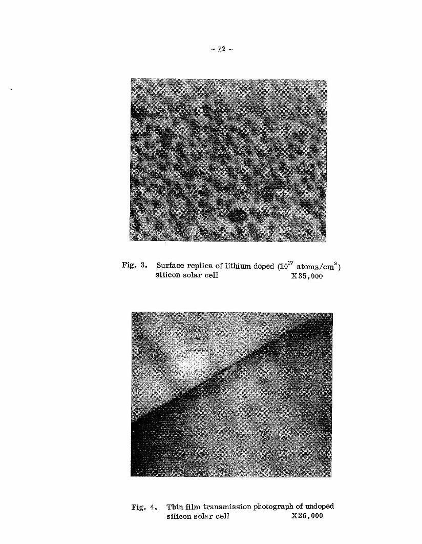
Fig. 3. Surface replica of lithium doped (10" atoms/crn3) silicon solar cell X 35,000
Fig. 4. Thin f i h transmission photograph of undoped silicon solar cell X25,OOO

very flat defect free region with very little structural detail, with the
exception of a grain boundary which runs diagonally across the photo-
graph. In the transmission photograph from the doped material, Figure
5, however, numerous small structural. defects can be observed through-
out the field, which a re indicative of the presence of precipitate particles.
Further evidence for the presence of precipitate particles in the
doped material is provided by careful examination of the electron diffraction
patterns from the doped and undoped thin film samples. Figure 6 shows
the diffraction pattern obtained from the undoped sample. The only
diffraction spots which can be observed a r e those which one would
expect from the diamond cubic lattice of silicon. An interpretive sche-
matic drawing of the above diffraction pattern with each spot indexed is
shown in Figure 7 (a). In Figure 8, however, which shows the diffraction
pattern obtained from the doped sample, a number of additional, but
weaker spots can be seen. An interpretive drawing of this diffraction
pattern is shown in Figure 7 (b). In this particular pattern the additional
diffraction spots can only be indexed satisfactorily as belonging to the bcc
crystal structure. Assuming the lattice parameter of silicon it is possible
to calculate the lattice parameter of the bcc structure by comparing the
radius ratios of the selected area diffraction spots. From such a cal-
culation, the lattice parameter of the bcc crystal structure was found to
be 3.45 which agrees very well with that for lithium. From this evidence
it appears that the precipitate particles observed in the doped silicon cells
a re probably due to excess lithium. From Figure 7 (b) it can be seen that
the 220 planes of the precipitate a re almost parallel (within 5') to the 220
planes of the silicon matrix.
The effective macroscopic cross section for the electron diffraction
was.approximately 5 microns squared. From a diffraction pattern such a s
this, it is impossible to estimate the specific number of microcrystallites
of the precipitated phase which a k giving rise to the additional diffraction
spots. Therefore, it is not possible to measure the density of the precip-
itates from selected area diffraction.

Fig. 5. Thin film transmission photograph of lithium
doped (loL7 atoms/cm3) silicon solar cell X25,OOO
Fig. 6 , Electron diffraction pattern from thin film of mdoped silicon solar cell.

Q 1 Double Oif Oraetiow
(229)
Fig. 7 (a). Interpretation of the diffraction pattern shown in Figure 6.
Zone Axis
(3111
Fig. 7 (b). Interpretation of the diffraction pattern shown in Figure 8.
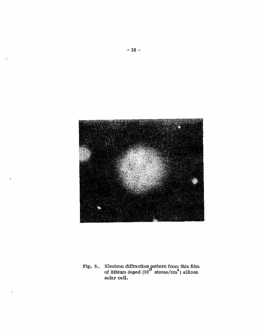
Fig. 8,. Electron diffraction attern from thin film IF of lithium doped (10 atoms/cm3) silicon solar cell.

Conclusions
Techniques have been established to etch and observe undoped
and lithium doped silicon solar cells by surface replication and
by thin film transmission electron microscopy.
From preliminary surface and thin film observations it appears
that a second phase precipitate exists in the doped cells which has
a bcc crystal structure and has a lattice parameter close to that of
lithium. Therefore, a s lithium is the only bcc material present in
any large amounts, it seems reasonable to conclude that in fact the
precipitates a re formed from excess lithium. (The above obser-
vations a re in agreement with the results of Berger, Horiye, Naber,
and Passenheim [19]. Recently they have carried out a neutron
activation analysis of lithium doped cells in which resistivity
measurements had indicated a lithium concentration of 1 0 ~ ~ a t o m / c m ~ , and in fact, they fomd that activation analysis indicated a concen-
tratioii up to eight times greater than this. They suggested the poss-
ibility that some lithium may be present as precipitates).
Plans for the Ned Reporting Period
During the next reporting period we plan to:
1. Irradiate undoped and doped lithium solar cells.
2. Study defects produced by neutron irradiation using surface replication
and thin film transmission electron microscopy.
3. Anneal the irradiation damage.
New Technology
No new technology is currently being developed o r employed in this
program.

REFERENCES
B, R. Gossick, J. Appl. Fhys. 30, 1214, (1959). - J. H. Crawford Jr. , and J. W. Cleland, J. Appl. Phys. , 2, 1204, (1959).
W. H. Closser, J. Appl. Phys. ,&I, 1693, (1960).
H. J. Stein, J. Appl. Phys., - 31, 1309, (1966).
H. J. Stein, Phys. , Rev. - 163, 801, (19671,
H. J. Stein, J. Appl. Pkys., - 39, 5283, (1968).
F. E. Fujita and U. Gonser, J. Phys. Soc. Japan, - 13, 1968, (1958).
J. R. Parsons, R. W. Balluffi and J. S. Koehler, Appl. Phys. Letters,
1, 57, (1962). - P. L. F. Hemment and E. Me Gunnersen, J. Appl. Phys., 37, 2912, (1966). - J. M. Pankratz, J. A. Sprague and M. L. Rudee, J. Appl. Phys. , 39, 101, (1968).
R. Chang, J. Appl. Phys., 2, 868, (1957).
T. S. Noggle and D. J. Stiegler, J. Appl. Phys., 38, 1279, (1959).
M. Bertolotti, T. Papa, D. Sette, V. Crasso and G. Vitali, Neuoro
Cimento, - 29, 1200, (1963)
M. Bertolotti, T. Papa, D. Sette, and G. Vitabi, J. Appl. Phys., 36, 3506, (1965).
M. Bertolotti, T. Papa, D, Sette, and G. Vitali, J. Appl. Phys., 3, 2645, (1967).
M. Bertolotti, "Radiation Effects in Semiconductors", Plenum Press . , 311, (1968).
G. R. Booker and R. Stickler, Brit. J. Appl. Phys., 13, 446, (1962).
R. P. Riesz and C. G. Bjorling, Rev. Sci., Instrum, - 32, 889, (1961).
R. A. Berger, H. Horiye, J. A. Naber, and B. C. Passenheim,
"Radiation Effects in Silicon Solar Cellstf, Quarterly Report to Je t
Propulsion Laboratory on Contract 952387, by Gulf General Atomic,
loth, October 1969.
For copies of publication or for other information address:
Office of Research and Engineering Services
Publication Services
College of Engineering
University of Kentucky
Lexington, Kentucky 40506
No part of this publication may be reproduced in any manner without written permission of the publisher. References to its content and quotations from it are permitted, provided the source is clearly indicated.