Embed Size (px)
Citation preview
Dept., of E.C.E, RCEW(3T),KNL.
B.TECH ELECTRONIC CIRCUIT ANALYSIS & DESIGN

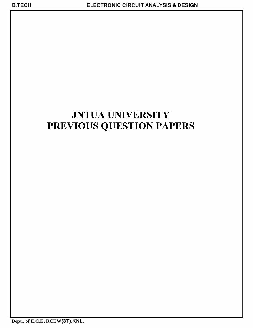
Code: 13A04402
B.Tech II Year II Semester (R13) Supplementary Examinations May/June 2017
ELECTRONIC CIRCUITS ANALYSIS & DESIGN (Common to ECE & EIE)
Time: 3 hours Max. Marks: 70
PART - A (Compulsory Question)
***** 1 Answer the following: (10 X 02 = 20 Marks) (a) What is a cascade amplifier? What is its advantage? (b) An amplifier consists of 3 identical stages in cascade. The bandwidth of overall amplifier extends from
20 Hz to 20 kHz. Calculate the bandwidth of individual stage. (c) Draw the small signal equivalent circuit for an emitter follower stage at high frequencies. (d) State Barkhausen criteria for sustained oscillations. (e) Distinguish between small signal and large signal amplifiers. (f) The following is an example of the output swing for a class ------- amplifier. Explain.
(g) Why gain bandwidth product remains constant with the introduction of negative feedback? (h) Why RC oscillators are not suitable for high frequency applications. (i) What is the fundamental difference between audio amplifier and tuned amplifier? (j) What is staggered tuning?
PART - B (Answer all five units, 5 X 10 = 50 Marks)
UNIT - I
2 (a) Discuss the classification of amplifiers based on frequency range and type of coupling, power delivered and signals handled.
(b) Design a single stage emitter follower having and . Assume
OR 3 (a) What are the different types of distortions possible in amplifier outputs? Explain. (b) For the circuit shown in figure below, calculate Ri, Ai, Av and Ro. Assume hie = 1.1 K, hfe = 50,
hre = 2.5 x 10⁻⁴, hoe = 25 .
Contd. in page 2
Page 1 of 2
R13
t OV
180 output
Swing
3 K
3 K
www.ManaResults.co.in

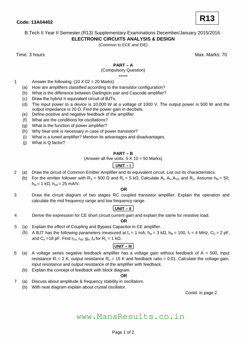
Code: 13A04402
UNIT - II
4 (a) Discuss the effect of emitter bypass capacitor and input & output coupling capacitors on the lower cut-off frequency if number of amplifiers are cascaded.
(b) The following low-frequency parameters are known for a given transistor at and at room temperature, , , , . At the same operating point, and , compute the values of all the hybrid – parameters.
OR 5 (a) Define and and derive the relation between and . (b) What are the typical values of various components in hybrid – p model? Show that at low frequencies
the hybrid – p model with and taken as infinite reduces to the approximate CE h – parameter model.
UNIT - III
6 (a) An amplifier with an open loop voltage gain of 1000 delivers 10 W of power output at 10% harmonic distortion when input is 10 mV. If 40dB negative feedback is applied and output power is to remain at 10 W, determine required input signal Vs and second harmonic distortion with feedback.
(b) Draw the circuit diagram of a RC phase shift oscillator using BJT. Derive the expression for frequency of oscillations.
OR 7 (a) Explain effect of negative feedback on gain, stability, distortion and bandwidth of an amplifier. (b) Discuss and explain the basic circuit of an LC oscillator and derive the condition for the oscillations.
UNIT - IV
8 (a) Explain with a neat circuit diagram, the working of a transformer coupled class A amplifier. Prove that the maximum efficiency is 50%.
(b) A transistor with a maximum junction temperature specification of 150 dissipates a maximum power of 40 watts at a case temperature of 25 and 2 watts at an ambient temperature of 25 . Find (i) The thermal resistance between the junction and the case. (ii) The thermal resistance between the junction and ambient. Maximum power dissipation capability for safe operation in free space at a temperature of 50
OR 9 (a) Derive the expression for maximum collector power dissipation Pc(Max) in the case of class B power
amplifiers. (b) What are the advantages and disadvantages of push pull configuration? Show that in class-B push pull
amplifier the maximum conversion efficiency is 78.5%.
UNIT - V
10 (a) Derive the expression for the 3dB bandwidth of a capacitance coupled single tuned amplifier. (b) Explain the principle of stabilizing the double tuned transformer coupled amplifier response against the
internal feedback. OR
11 (a) Explain the reasons for oscillations in a tuned amplifier. Briefly explain the methods used to stabilize the tuned amplifiers against oscillations.
(b) Explain the operation of a double tuned amplifier. Explain the advantages of double tuned circuit over single tuned circuit.
*****
Page 2 of 2
R13
www.ManaResults.co.in

Code: 13A04402
B.Tech II Year II Semester (R13) Supplementary Examinations December 2016
ELECTRONIC CIRCUITS ANALYSIS & DESIGN (Common to ECE and EIE)
Time: 3 hours Max. Marks: 70 PART – A
(Compulsory Question)
***** 1 Answer the following: (10 X 02 = 20 Marks) (a) Define class AB amplifier. (b) Write the advantages of transformer coupling. (c) Calculate hfe for short circuit current gain of transistor is 25 at a frequency of 2 MHz, if (d) An amplifier has a value of Rin = 4.2 k , AV = 220 and Determine the value of input resistance of
the feedback amplifier. (e) Write the advantages of negative feedback amplifier. (f) A wein-bridge oscillator has a frequency of 500 Hz, if the value of C is 100 pF, determine the value of R. (g) Describe the types of heat sinks. (h) Explain FET as voltage variable resistor. (i) What are the advantages of the double tuning? (j) Define the Q – factor in tuned circuits.
PART – B
(Answer all five units, 5 X 10 = 50 Marks)
UNIT – I
2 Explain RC-coupled CE transistor stages. Show the middle and low frequency model for one stage. Write the expressions for current gains.
OR 3 With a neat diagram, analyze the complementary Darlington transistor.
UNIT – II
4 Derive the expression for CE short circuit current gain Ai as a function of frequency using hybrid – π model.
OR 5 Write a short note on gain bandwidth product of amplifier and derive the expression on the following: (a) Product of voltage. (b) Product of current.
UNIT – III
6 What are the different types of negative feedback? Briefly explain how the input and output impedances of an amplifier are affected by the different types of negative feedback.
OR 7 Draw the circuit diagram of current shunt feedback and derive expressions for input and output
resistances.
UNIT – IV
8 Draw the push pull power amplifier circuit. Derive the expression for the output current in push amplifier with base current as Ib = Ibn sin(wt).
OR 9 Explain the thermal run away, thermal resistance, thermal stability and thermal instability factors.
UNIT – V
10 Derive the expression for quality factor of a single tuned inductively coupled amplifier. OR
11 What is the importance of stagger tuning? Explain briefly about stagger-tuned amplifier.
*****
R13
www.ManaResults.co.in

Code: 13A04402
B.Tech II Year II Semester (R13) Regular Examinations May/June 2015 ELECTRONIC CIRCUITS ANALYSIS & DESIGN
(Common to ECE & EIE) Time: 3 hours Max. Marks: 70
PART – A (Compulsory question)
*****
1 Answer the following: (10 X 02 = 20 Marks) (a) Voltage gain of a single stage amplifier is 30. Bandwidth is 20 kHz. Two such stages are cascaded. Find the overall
voltage gain and bandwidth. (b) List out the advantages and disadvantages of RC coupled amplifier. (c) Draw the frequency response of RC coupled amplifier and indicate bandwidth, low, mid and high frequency ranges. (d) A multistage amplifier is to be constructed using four identical stages, each of which has a lower cutoff frequency 15
Hz and upper cutoff frequency 30 kHz. What will be the lower and upper cutoff frequency of the multistage amplifier? (e) Draw the equivalent circuit of transconductance amplifier. (f) An amplifier has a gain of 300, when the -ve feedback is applied gain is reduced to 240. Find feedback factor. (g) Differentiate between power amplifier and voltage amplifier. (h) What are the advantages of push pull amplifier configuration? (i) List out the advantages of tuned circuit. (j) Distinguish between single tuned and double tuned amplifiers. PART – B
(Answer all five units, 5 X 10 = 50 Marks)
UNIT – I 2 (a) Explain the effect of cascading of amplifiers on bandwidth. (b) Compare various coupling schemes used in amplifiers. (OR)
3 (a) Give the analysis of transformer coupled amplifier in mid band region. (b) Derive the expression for voltage gain and current gain of cascade amplifier.
UNIT – II 4 (a) Draw the small signal simplified hybrid equivalent circuit of an CE amplifier and discuss the effect of bypass capacitor
on the frequency response of an amplifier. (b) Determine the low frequency response of CE amplifier using the following specifications:
(OR) 5 (a) Draw the hybrid – π model for a transistor in CE configuration and explain the significance of each component in the
model. (b) Explain the variation of hybrid parameters with increasing | |, | | and temperature.
UNIT – III 6 (a) What is the effect of –ve feedback on the input impedance of an amplifier? (b) Derive the expression for frequency of oscillations of RC phase shift oscillator. (OR)
7 (a) State and explain Barkhausen’s criteria. (b) Explain the working of Hartley oscillator. Also derive the expression for its frequency of oscillations.
UNIT – IV 8 (a) Show the conversion efficiency of transformer coupled class A amplifier is 50%. (b) Explain the operations of class B push pull amplifier. (OR)
9 (a) Explain ideal and practical performance of class–D amplifier. (b) What is cross over distortion? Explain how it can be eliminated.
UNIT – V 10 Explain the operation of a single tuned capacitive coupled amplifier and derive the expression for bandwidth.
(OR) 11 (a) Define resonant frequency and derive an expression for the impedance of tuned circuit.
(b) What are the limitations of single tuned amplifiers?
R13
www.ManaResults.co.in

Code: 13A04402
B.Tech II Year II Semester (R13) Supplementary Examinations December/January 2015/2016
ELECTRONIC CIRCUITS ANALYSIS & DESIGN (Common to ECE and EIE)
Time: 3 hours Max. Marks: 70
PART – A (Compulsory Question)
***** 1 Answer the following: (10 X 02 = 20 Marks) (a) How are amplifiers classified according to the transistor configuration? (b) What is the difference between Darlington pair and Cascode amplifier? (c) Draw the hybrid π equivalent circuit of BJTs. (d) The input power to a device is 10,000 W at a voltage of 1000 V. The output power is 500 W and the
output impedance is 20 Ω. Find the power gain in decibels. (e) Define positive and negative feedback of the amplifier. (f) What are the conditions for oscillations? (g) What is the function of power amplifier? (h) Why heat sink is necessary in case of power transistor? (i) What is a tuned amplifier? Mention its advantages and disadvantages. (j) What is Q factor?
PART – B
(Answer all five units, 5 X 10 = 50 Marks)
UNIT – I
2 (a) Draw the circuit of Common Emitter Amplifier and its equivalent circuit. List out its characteristics. (b) For the emitter follower with RS = 500 Ω and RL = 5 kΩ, Calculate AI, AV,AVS and Ro. Assume hfe = 50,
hie = 1 kΩ, hoe = 25 mA/V. OR
3 Draw the circuit diagram of two stages RC coupled transistor amplifier. Explain the operation and calculate the mid frequency range and low frequency range.
UNIT – II
4 Derive the expression for CE short circuit current gain and explain the same for resistive load. OR 5 (a) Explain the effect of Coupling and Bypass Capacitor in CE amplifier. (b) A BJT has the following parameters measured at Ιc = 1 mA; hie = 3 kΩ, hfe = 100, fT = 4 MHz, CC = 2 pF,
and Ce =18 pF. Find rb’e, rbb’, gm ,fH for RL = 1 kΩ.
UNIT – III
6 (a) A voltage series negative feedback amplifier has a voltage gain without feedback of A = 500, input resistance Ri = 2 K, output resistance Ro = 15 K and feedback ratio = 0.01. Calculate the voltage gain, input resistance and output resistance of the amplifier with feedback.
(b) Explain the concept of feedback with block diagram. OR
7 (a) Discuss about amplitude & frequency stability in oscillators. (b) With neat diagram explain about crystal oscillator.
Contd. in page 2
Page 1 of 2
R13
www.ManaResults.co.in

Code: 13A04402
UNIT – IV
8 (a) Draw the circuit diagram of class-A power amplifier with transformer coupled. Explain operation and calculate the efficiency.
(b) What are the advantages and disadvantages of push pull configuration? Show that in class –B push pull amplifier the maximum conversion efficiency is 78.5%.
OR 9 (a) A transistor in a transformer coupled (class – A) power amplifier has to deliver a maximum of 5 W to a
load of 4 Ω. The quiescent point is adjusted for symmetrical swing, and the collector supply voltage is VCC = 20 Volts. Assume Vmin = 0 volts. (i) What is the transformer turns ratio? (ii) What is the peak collector current?
(b) Compare the series fed and transformer coupled class – A power amplifiers. Why is the conversion efficiency doubled in transformer coupled class – A amplifier?
UNIT – V
10 (a) Explain the working of single tuned amplifier. Draw the frequency response (b) Explain the operation of a double tuned amplifier. Explain the advantages of double tuned circuit over
single tuned circuit OR
11 (a) Explain the effect of cascading single tuned amplifier on band width (b) Derive the expression for bandwidth in terms of resonant frequency and quality factor in case of double
tuned amplifiers.
*****
Page 2 of 2
R13
www.ManaResults.co.in
Code: 13A04402
B.Tech II Year II Semester (R13) Supplementary Examinations December/January 2015/2016
ELECTRONIC CIRCUITS ANALYSIS & DESIGN (Common to ECE and EIE)
Time: 3 hours Max. Marks: 70
PART – A (Compulsory Question)
***** 1 Answer the following: (10 X 02 = 20 Marks) (a) How are amplifiers classified according to the transistor configuration? (b) What is the difference between Darlington pair and Cascode amplifier? (c) Draw the hybrid π equivalent circuit of BJTs. (d) The input power to a device is 10,000 W at a voltage of 1000 V. The output power is 500 W and the
output impedance is 20 Ω. Find the power gain in decibels. (e) Define positive and negative feedback of the amplifier. (f) What are the conditions for oscillations? (g) What is the function of power amplifier? (h) Why heat sink is necessary in case of power transistor? (i) What is a tuned amplifier? Mention its advantages and disadvantages. (j) What is Q factor?
PART – B
(Answer all five units, 5 X 10 = 50 Marks)
UNIT – I
2 (a) Draw the circuit of Common Emitter Amplifier and its equivalent circuit. List out its characteristics. (b) For the emitter follower with RS = 500 Ω and RL = 5 kΩ, Calculate AI, AV,AVS and Ro. Assume hfe = 50,
hie = 1 kΩ, hoe = 25 mA/V. OR
3 Draw the circuit diagram of two stages RC coupled transistor amplifier. Explain the operation and calculate the mid frequency range and low frequency range.
UNIT – II
4 Derive the expression for CE short circuit current gain and explain the same for resistive load. OR 5 (a) Explain the effect of Coupling and Bypass Capacitor in CE amplifier. (b) A BJT has the following parameters measured at Ιc = 1 mA; hie = 3 kΩ, hfe = 100, fT = 4 MHz, CC = 2 pF,
and Ce =18 pF. Find rb’e, rbb’, gm ,fH for RL = 1 kΩ.
UNIT – III
6 (a) A voltage series negative feedback amplifier has a voltage gain without feedback of A = 500, input resistance Ri = 2 K, output resistance Ro = 15 K and feedback ratio = 0.01. Calculate the voltage gain, input resistance and output resistance of the amplifier with feedback.
(b) Explain the concept of feedback with block diagram. OR
7 (a) Discuss about amplitude & frequency stability in oscillators. (b) With neat diagram explain about crystal oscillator.
Contd. in page 2
Page 1 of 2
R13
www.ManaResults.co.in
Code: 13A04402
UNIT – IV
8 (a) Draw the circuit diagram of class-A power amplifier with transformer coupled. Explain operation and calculate the efficiency.
(b) What are the advantages and disadvantages of push pull configuration? Show that in class –B push pull amplifier the maximum conversion efficiency is 78.5%.
OR 9 (a) A transistor in a transformer coupled (class – A) power amplifier has to deliver a maximum of 5 W to a
load of 4 Ω. The quiescent point is adjusted for symmetrical swing, and the collector supply voltage is VCC = 20 Volts. Assume Vmin = 0 volts. (i) What is the transformer turns ratio? (ii) What is the peak collector current?
(b) Compare the series fed and transformer coupled class – A power amplifiers. Why is the conversion efficiency doubled in transformer coupled class – A amplifier?
UNIT – V
10 (a) Explain the working of single tuned amplifier. Draw the frequency response (b) Explain the operation of a double tuned amplifier. Explain the advantages of double tuned circuit over
single tuned circuit OR
11 (a) Explain the effect of cascading single tuned amplifier on band width (b) Derive the expression for bandwidth in terms of resonant frequency and quality factor in case of double
tuned amplifiers.
*****
Page 2 of 2
R13
www.ManaResults.co.in


Code: 13A04402
B.Tech II Year II Semester (R13) Supplementary Examinations May/June 2019
ELECTRONIC CIRCUITS ANALYSIS & DESIGN (Common to ECE & EIE)
Time: 3 hours Max. Marks: 70
PART – A (Compulsory Question)
***** 1 Answer the following: (10 X 02 = 20 Marks) (a) Explain about the classification of amplifiers based on type of coupling and bandwidth. (b) What is Darlington transistor? What are its salient features? (c) Define 𝑓𝛽 and 𝑓𝑇 and derive the relation between 𝑓𝛽 and 𝑓𝑇. (d) Reason out the causes and results of phase & frequency distortions in transistor amplifiers. (e) Distinguish between regenerative and degenerative feedback in amplifiers. (f) Classify different type of oscillators based on frequency range. (g) Explain the origin of crossover distortion, how to minimize this distortion. (h) Compare the advantages and disadvantages of class-B push pull and class-B complementary
symmetry power amplifiers. (i) Compare single tuned and double tuned amplifiers. (j) State the functions and frequency ranges of operation of tuned amplifiers with relevant reasons.
PART – B
(Answer all five units, 5 X 10 = 50 Marks)
UNIT – I
2 The h-parameters of CE-amplifier are hie = 1100 Ω, hre = 2.5 × 10⁻⁴, hfe = 50, hoe = 24 µA/V and RS = 1 kΩ, RL = 10 kΩ. Find out current and voltage gains with and without source resistance, input and output impedances.
OR 3 With the help of a neat circuit diagram, describe the working of a cascode amplifier. Explain the
properties of cascode amplifier.
UNIT – II
4 Derive the expression for the CE short circuit current gain Ai as a function of frequency using hybrid- 𝜋 model.
OR 5 Draw the frequency response of an amplifier and explain the effects of coupling and bypass
capacitors.
UNIT – III
6 An amplifier circuit has a gain of 60dB and an output impedance Zo = 10 kΩ. It is required to modify its output impedance to 500 Ω by applying negative feedback. Calculate the value of the feedback factor. Also find the percentage change in the overall gain, for 10% change in the gain of the internal amplifiers.
OR 7 Show that the gain of Wien bridge oscillator using BJT amplifier must be at least 3 for the oscillations
to occur. Contd. in page 2
Page 1 of 2
R13

Code: 13A04402
UNIT – IV
8 Derive the equation for maximum efficiency of a class A transformer coupled amplifier. OR
9 In complementary – symmetry class-B power amplifier circuit, VCC = 25 volts; RL = 16 and Imax = 2 amps. Determine the input power, output power and efficiency.
UNIT – V
10 Draw the circuit of double-tuned transformer-coupled amplifier. Discuss the nature of responses of the amplifier for different values of KQ = 1; KQ>1 and KQ<1.
OR 11 Explain the principle of stagger tuning technique of transformer – coupled amplifier that is used to
obtain band pass filter characteristic with pass band of 10 kHz with all necessary diagrams for illustration.
*****
Page 2 of 2
R13


![Oscillations mécaniques libres non amorties Oscillations ...ww2.cnam.fr/physique/PHR004/04_L08_PHR004.pdf · Leçon n°8 : Oscillations [1] PHR 004 1 Oscillations mécaniques libres](https://img.dokumen.tips/doc/110x75/5b968ab509d3f206218b9064/oscillations-mecaniques-libres-non-amorties-oscillations-ww2cnamfrphysiquephr00404l08.jpg)