Embed Size (px)
Citation preview

ETG300ETG300DRETG250ETG250DR
USER AND MAINTENANCE MANUAL
TECHNICAL ANNEX
Via G. Amendola 9 - 44028 Poggio Renatico (FE) - ItalyPhone. +39 0532 829 965 - Fax +39 0532 829 177E-Mail: [email protected] address: www.elenos.com
Edition 1Rev. 1 - 14/05/2001
Cod. MAN0075
BROADCAST EQUIPMENT COMPANY

Use and maintenance manual
Page 2 Engineering Department PHONE: +39 0532 829 965 - FAX: +39 0532 829 177E-Mail: [email protected]
Firstly, thank you for choosing an product.
products are solid state or thermionic tube transmitters that develop power from a minimum of 20W to a maximum of 30KW.
Great care has been taken during the design of the protection circuitry to ensure compa-tability with products from other manufacturers. However the best performance is achie-ved when the equipment is used with other products manufactured by .
The unit has been designed to guarantee consistent performance over time, without the need for special maintenance. The need for this is minimised by regular functional checks of those components which are ventilated.
Operation of the unit is very easy and intuitive. Even so it is recommended that this manual and other relevant documentation is read carefully before any operation is attempted.
Dear User,
Customer Care

Use and maintenance manual
Page 3Engineering Department PHONE: +39 0532 829 965 - FAX: +39 0532 829 177E-Mail: [email protected]
INDEX
CONTENTS
1. GENERAL 1.1. Front View...................................................................................Page 5 1.1.1. Front panel description.......................................................Page 5 1.2. Rear View....................................................................................Page 7 1.2.1. Rear panel description........................................................Page 7
2. INSTALLATION......................................................................................Page 9
3. USER INSTRUCTIONS 3.1. User interface..............................................................................Page 10 3.2. Telemetry connection and operation ..............................................Page 11 3.3. Powering up ................................................................................Page 13 3.4. Description of the graphics interface, setup and measurement 3.4.1. Main menu .......................................................................Page 14 3.4.2. Functions menu .................................................................Page 15 3.4.3. Audio menu - Input signal level adjustment ..........................Page 16 3.4.4. RF menu - Output power adjustment ...................................Page 17 3.4.5. Frequency menu - Frequency programming..........................Page 18 3.4.6. User setup menu................................................................Page 19 3.4.7. Timer display .....................................................................Page 20 3.4.8. RDS menu - RDS adjustment and programming (optional) .....Page 21 3.4.9. Deviation e Statistics menu .................................................Page 25 3.4.10. RDS encoder programming ................................................Page 27 3.5. Checking performance.................................................................Page 39
4. GENERAL DESCRIPTION 4.1. Introduction.................................................................................Page 41 4.2. Using the block diagram ..............................................................Page 41 4.3. Block diagram 4.3.1. Transformer version............................................................Page 43* 4.3.2. Switch-mode version ..........................................................Page 45* 4.4. Power supply section ....................................................................Page 47 4.4.1. Services ............................................................................Page 47 4.4.2. Power 4.4.2.1. Switch-mode version .....................................................Page 47 4.4.2.2. Transformer version.......................................................Page 48 4.5. Radio frequency section ...............................................................Page 48 4.5.1. Driver ...............................................................................Page 48 4.5.2. RF module ........................................................................Page 49 4.5.3. Low-pass filter ...................................................................Page 49 4.5.4. Probe 4.5.4.1. Output power measurement ..........................................Page 49 4.5.4.2. AGC protection ............................................................Page 49 4.6. Logic (Mother board) ...................................................................Page 50 4.6.1. CPU board........................................................................Page 50 4.6.2. ALC board ........................................................................Page 50 4.6.3. VCO/PLL board.................................................................Page 50 4.6.4. MPX board ........................................................................Page 50 4.7. Keyboard ....................................................................................Page 50 4.8. Optional boards..........................................................................Page 51 4.8.1. Stereo input board .............................................................Page 51 4.8.2. Stereo encoder board ........................................................Page 52

Use and maintenance manual
Page 4 Engineering Department PHONE: +39 0532 829 965 - FAX: +39 0532 829 177E-Mail: [email protected]
INDEX
4.8.3. RDS board ........................................................................Page 53
5. ELECTRICAL SCHEMATICS 5.1. Auxiliary power supply 5.1.1. Layout...............................................................................Page 57 5.1.2. Schematic .........................................................................Page 59* 5.1.3. Parts list ............................................................................Page 61 5.2. Switching power supply 5.2.1. Layout...............................................................................Page 63 5.2.2. Schematic .........................................................................Page 65* 5.2.3. Parts list ............................................................................Page 67 5.3. Mother board 5.3.1. Layout...............................................................................Page 71* 5.3.2. Schematics 5.3.2.1. VCO ...........................................................................Page 73* 5.3.2.2. PLL ..............................................................................Page 75* 5.3.2.3. MPX ............................................................................Page 77* 5.3.2.4. AGC and SWR protection..............................................Page 79* 5.3.2.5. CPU ............................................................................Page 81* 5.3.3. Parts list ............................................................................Page 83 5.4. Keyboard 5.4.1. Layout...............................................................................Page 93 5.4.2. Schematic .........................................................................Page 95* 5.4.3. Parts list ............................................................................Page 97 5.5. Driver 5.5.1. Layout...............................................................................Page 99 5.5.2. Schematic .........................................................................Page 100 5.5.3. Parts list ............................................................................Page 101 5.6. RF final output stage 5.6.1. Layout...............................................................................Page 103 5.6.2. Schematic .........................................................................Page 104 5.6.3. Parts list ............................................................................Page 105 5.7. LP filter 5.7.1. Layout...............................................................................Page 107 5.7.2. Schematics 5.7.2.1. Directional coupler .......................................................Page 108 5.7.2.2. Directional coupler amplifier..........................................Page 109 5.7.2.3. Low-pass filter ..............................................................Page 110 5.7.3. Parts list ............................................................................Page 111 5.8. Input output combiner system 5.8.1. Schematic .........................................................................Page 113 5.9. BUS board 5.9.1. Layout...............................................................................Page 115 5.9.2. Schematic .........................................................................Page 116 5.9.3. Parts list ............................................................................Page 117 5.10. Thermal probe 5.10.1. Layout...............................................................................Page 119 5.10.2. Schematic .........................................................................Page 119 5.10.3. Parts list ............................................................................Page 120
6. TROUBLESHOOTING ...........................................................................Page 121
7. TECHNICAL SPECIFICATION .................................................................Page 123
Page numbers marked with an asterisk (*) are in A3 format

Use and maintenance manual
Page 5Engineering Department PHONE: +39 0532 829 965 - FAX: +39 0532 829 177E-Mail: [email protected]
1. GENERAL
1 5432 6
1.1.Front view
1) Power on switch2) Switches for programming operation3) Led: “ON AIR” lit, indicates the PLL has reached the desired frequency “FAILURE” lit, indicates the output power is below the preset threshold “MAINS” lit, indicates the unit is switched on4) The “RF monitor” connector provides an RF monitor signal5) The “MPX OUT” connector provides an audio signal6) Display
N.B.Do not obstruct the ventilation grills
1.1.1.Front Panel description

Use and maintenance manual
Page 6 Engineering Department PHONE: +39 0532 829 965 - FAX: +39 0532 829 177E-Mail: [email protected]
1. GENERAL
Use and maintenance manual
Page 7Engineering Department PHONE: +39 0532 829 965 - FAX: +39 0532 829 177E-Mail: [email protected]
1. GENERAL
1 5432 6 7 8 9 10 11 12
13
15141.2.
Rear view
1.2.1.Rear Panel description
1) “RF OUT” connector2) Earthing terminal3-4) Power supply fuse (10A)5) Line supply socket6) Analog signal interface7) Telemetry interface8) “MPX” input connector9) “SCA2” input connector10) Trimmer for calibrating the “SCA2” input11) “SCA1” input connector12) Trimmer for calibrating the “SCA1” input13) Slot for inserting the stereo encoder board14) Slot for inserting the RDS board15) Slot for inserting the stereo inputs board
N.B.Do not obstruct the ventilation grills

Use and maintenance manual
Page 8 Engineering Department PHONE: +39 0532 829 965 - FAX: +39 0532 829 177E-Mail: [email protected]
1. GENERAL

Use and maintenance manual
Page 9Engineering Department PHONE: +39 0532 829 965 - FAX: +39 0532 829 177E-Mail: [email protected]
2. INSTALLATION
2.Installation
Remove the unit from its packaging and before attempting any operation, check that the unit has not been damaged during transport and that all the switches and con-nectors located on the front and rear panels are serviceable.
Install the unit so that it is accessible from all sides Ensure that the location of the unit allows for connection to an efficient earthing point Ensure that the antenna system is suitable Check that any amplifier to be eventually connected downstream is connected to the antenna system
Connect the appropriate inputs of the exciter according to the type of operation requi-red:
the monophonic signal to the XLR connector on the mono board the stereo signal (low frequency) to the left and right XLR connectors on the stereo
input board the stereo signal (wide-band) to the MPX connector on the MPX and SCA inputs
board the RDS signal to one of the two SCA connectors on the MPX and SCA inputs
board If the RDS board is fitted, the wide-band stereo signal goes directly to the MPX
inputs on the RDS board, so the MPX+RDS output will be connected to the MPX input on the MPX and SCA inputs board.
Connect the electricity supply cable Connect the RF output to the input of any amplifier to be used, or to the antenna system
Switch on the amplifier (if present) In order to verify that the equipment is functioning correctly, check the values displayed by the exciter and amplifier displays and instrumentation

Use and maintenance manual
Page 10 Engineering Department PHONE: +39 0532 829 965 - FAX: +39 0532 829 177E-Mail: [email protected]
3. USER INSTRUCTIONS
123456789
10111213141516171819202122232425
IN1 = SB_ONIN2 = SB_OFFGNDGNDIN3 = VDS 5V.F.S.IN4 = IDRAIN 5V.F.S.NCIN5 = LOCK REM.IN6 = +5V. REM.IN7 = RPW REM.IN8 = CUR REM.IN9 = IPW REM.IN10 = V. REF. REM.GNDGNDNCGNDIN11 = STAND-BYIN12 = REF. PWR 1V.F.S.IN13 = DIR PWR 3.6V.F.S.IN14 = TMP REM.IN15 = VPW REM. IN16 = FPW REM.IN17 = -12V. REM.IN18 = +12V. REM.
3.1.User interface
The user interface is designed to accept upto 14 analog signals in the range 0 to 2V. For example, it is possible to read a remote temperature, remote voltages and currents of other equipment and direct and reflected power of other equipment.
Pins with an “IN” prefix are inputsPins with an “NC” prefix are not connectedPins with a “GND” prefix are earths
To enable external RF OFF function (stand by) after having switched on the device, during countdown, press P2 and P7 at the same time, enter the password (2222, press P2 four times) enable “EXT RF OFF” and save the new configuration.

Use and maintenance manual
Page 11Engineering Department PHONE: +39 0532 829 965 - FAX: +39 0532 829 177E-Mail: [email protected]
3. USER INSTRUCTIONS
1 TX2 TX3 RX4 RX5 GND6 GND7 GND8 GND9 GND
DCD 1RxD 2TxD 3DTR 4GND 5DSR 6RTS 7CTS 8
RI 9
1 TX2 TX3 RX4 RX5 GND6 GND7 GND8 GND9 GND
DCD 1RxD 2TxD 3DTR 4GND 5DSR 6RTS 7CTS 8
RI 9
DB9 Male - DB9 Female
DB9 Male - DB9 Male
ETG250 (300) --------> Modem
ETG250 (300) --------------> PCFM TRANSMITTER
FM TRANSMITTER
3.2.Telemetry
Connectionand operation
The ETG250’s (ETG300’s) telemetry feature allows an IBM compatible PC to be connected directly to the unit, or via a GSM modem. The main operational parameters can be displayed and modified via telemetry using the Hyper Terminal software supplied with any version of Microsoft Windows (c).
Connect the unit to a GSM modem, or directly to a PC, using the cable supplied (see diagram below).
Run the Hyper Terminal software supplied with Microsoft Windows. Enable the connection (to connect via modem, refer to the configuration in the GSM modem manual). Telemetry will now be available on the PC, but to transfer data, the code $1111 must be entered; only then may the unit’s parameters be displayed and modified.

Use and maintenance manual
Page 12 Engineering Department PHONE: +39 0532 829 965 - FAX: +39 0532 829 177E-Mail: [email protected]
3. USER INSTRUCTIONS
3.2.Telemetry
Connection and operation
Main Screen
The following parameters can viewed on the main screen: the programmed fre-quency, the status of the PLL, the status of pre-emphasis, the level of direct power, the level of reflected power and the audio level. From this screen the output power can be increased or decreased by pressing the “P” key with either the “+” or “-” keys respectively. Once the desired value has been reached, it can be saved by pressing the “S” key. To modify the frequency, press the “F” key with either the “+” or “-” keys to incre-ase or decrease the frequency respectively. Once the desired frequency has been reached, it can be saved by pressing the “S” key. To terminate transmission of data, type “$C”. Pressing the “H” (help) key will open the help screen where all the above com-mands are identified (see diagram below).
Press the “M” (Main) key to return to the main screen.

Use and maintenance manual
Page 13Engineering Department PHONE: +39 0532 829 965 - FAX: +39 0532 829 177E-Mail: [email protected]
3. USER INSTRUCTIONS
3.3.Powering up
The start up screen appears showing the state of the audio BUS. The microprocessor runs a system check to verify which optional boards have been
fitted. The countdown starts (duration 8 seconds) after which the exciter will develop power.
Pressing keys during the countdown: Pressing any key will prevent power from being developed Pressing F1+F8 will terminate the countdown
On termination of the countdown, the main menu will appear (with the ELENOS logo or that of the customer)
FM TRANSMITTER
FM TRANSMITTER
98.10

Use and maintenance manual
Page 14 Engineering Department PHONE: +39 0532 829 965 - FAX: +39 0532 829 177E-Mail: [email protected]
3. USER INSTRUCTIONS
3.4.1.Main Menu
Press key P1 to access the menu functions Press key P2 to increase the contrast of the display Press key P3 to reduce the contrast of the display Press key P4 repetitively to select the desired language
The language of the display will change each time the key is pressed The language selected will be indicated by a letter under the ELENOS logo.
Press key P5 to display the time for which the unit has been operated.
The main menu displays respectively: MPX level, direct power, reflected power, opera-ting frequency, PLL lock, clipper operation, insertion of pre-emphasis and insertion of the stereo encoder. The logo displayed by the unit can be personalised on the request of the user. The default logo is that of ELENOS with which is also displayed the version of software instal-led (e.g. V4.08) and the language selected (e.g. UK)
FM TRANSMITTER
98.10

Use and maintenance manual
Page 15Engineering Department PHONE: +39 0532 829 965 - FAX: +39 0532 829 177E-Mail: [email protected]
3. USER INSTRUCTIONS
3.4.2.Functions Menu
Press key P1 to access the audio menu Press key P2 to access the RF menu Press key P3 to access the frequency programming menu Press key P4 to access the RDS menu if the optional RDS board is fitted Press key P5 to access the user setup menu Press key P6 to access the deviation and statistics menu
The following parameters are displayed in the Functions menu: MPX level, direct power, reflected power, operating frequency, PLL lock, clipper operation, insertion of pre-emphasis and activation of the stereo encoder. Once the functions menu has been entered, if no key is pressed, the main menu will automatically appear after 10 seconds.
FM TRANSMITTER
98.10

Use and maintenance manual
Page 16 Engineering Department PHONE: +39 0532 829 965 - FAX: +39 0532 829 177E-Mail: [email protected]
3. USER INSTRUCTIONS
3.4.3.Audio Menu
Press key P1 to return to the functions menu Press key P4 to set the input signal level (default 0dBm) Press key P2 to reduce the input signal level Press key P3 to increase the input signal level Press key P6 to save the adjustment made Press key P5 to disable or re-enable the audio signal
The audio menu displays the following parameters: direct power, reflected power and MPX signal level in both “analog” and numerical form. In the diagram direct power is disabled (RF OFF), the reflected power is 0W and the MPX signal level is -21dBm. If the stereo encoder is present, the indication of direct and reflected power is replaced by the level of the signals on the left and right channels.
Adjustment of the input signal level
FM TRANSMITTER
0.0-21.0

Use and maintenance manual
Page 17Engineering Department PHONE: +39 0532 829 965 - FAX: +39 0532 829 177E-Mail: [email protected]
3. USER INSTRUCTIONS
3.4.4.RF Menu
Press key P1 to return to the functions menu Press key P4 to set the output power level from 0W to a maximum value of 500W Press key P2 to reduce the output power Press key P3 to increase the output power Press key P6 to save the adjustment made Press key P7 to activate or disactivate the output stage of the amplifier. For example,
in the diagram, output power is disabled.
In the RF menu, the following parameters are displayed: direct power, reflected power and temperature in both “analog” and numerical form.
Adjustment of output power
FM TRANSMITTER
0.075.2

Use and maintenance manual
Page 18 Engineering Department PHONE: +39 0532 829 965 - FAX: +39 0532 829 177E-Mail: [email protected]
3. USER INSTRUCTIONS
3.4.5.Frequency Menu
Press key P1 to return to the functions menu Press key P4 to set the operating frequency Press key P2 to reduce the operating frequency Press key P3 to increase the operating frequency Press key P6 to save the adjustment made
The frequency menu displays the following parameters: MPX level, direct power, reflected power, operating frequency (highlighted), PLL lock, clipper operation, insertion of pre-emphasis and activation of the stereo encoder.
Adjustment of output frequency
FM TRANSMITTER
98.10
98.10

Use and maintenance manual
Page 19Engineering Department PHONE: +39 0532 829 965 - FAX: +39 0532 829 177E-Mail: [email protected]
3. USER INSTRUCTIONS
3.4.6.User setup menu
Press key P1 to return to the functions menu Press key P2 to scroll the menu options from top to bottom Press key P3 to scroll the menu options from bottom to top Press key P4 to enable (circle filled) or disable (circle empty) the selected function Press key P6 to save the change Press key P5 to program a four figure password
The password restricts access to the audio, frequency, power and user setup menus by unauthorised personnel.The following parameters are displayed in the user setup menu: MPX level, direct power, reflected power, operating frequency, PLL lock, clipper operation, insertion of pre-empha-sis and activation of the stereo encoder.
FM TRANSMITTER
98.10

Use and maintenance manual
Page 20 Engineering Department PHONE: +39 0532 829 965 - FAX: +39 0532 829 177E-Mail: [email protected]
3. USER INSTRUCTIONS
3.4.7.Timer Display
From the main menu, key P5 accesses the timer display which indicates the ope-rating time of the unit in days (d), hours (h) and minutes (m).
FM TRANSMITTER
98.10
WORK: 0003d 17h 62m

Use and maintenance manual
Page 21Engineering Department PHONE: +39 0532 829 965 - FAX: +39 0532 829 177E-Mail: [email protected]
3. USER INSTRUCTIONS
3.4.8.RDS menu(Optional)
Adjustment of RDS settings (optional)
In function menu press P4 to enter RDS menu
Press P1 to return to function menu Press P2 to enable RDS messaging settings Press P3 to enable alternative frequencies settings Press P4 to enable radio text settings Press P5 to enable groups settings Press P6 to set RDS Date and Time, PTY, DI, TA, TP, MS and PI Press P8 to save settings
FM TRANSMITTER

Use and maintenance manual
Page 22 Engineering Department PHONE: +39 0532 829 965 - FAX: +39 0532 829 177E-Mail: [email protected]
3. USER INSTRUCTIONS
3.4.8.RDS Menu(Optional)
From the RDS menu (page 21) Press key P6 to program RDS Date and Time, PTY, DI, TA, TP, MS and PI
Press key P1 to return to the main RDS menu Press keys P4 and P5 to select the data to modify Press keys P2 and P3 to select options for the selected data Press key P6 to save the changes made
FM TRANSMITTER

Use and maintenance manual
Page 23Engineering Department PHONE: +39 0532 829 965 - FAX: +39 0532 829 177E-Mail: [email protected]
3. USER INSTRUCTIONS
From the RDS menu (page 21) Press key P4 to set the RDS TEXT message
Press key P1 to return to the main RDS menu Press keys P4 and P5 move the cursor Press keys P2 and P3 to select the letter to insert Press key P6 to save the changes made to the message
N.B. If unsaved, the previous message will remain unchanged Press key P8 to delete the whole message
3.4.8.RDS Menu(Optional)
FM TRANSMITTER

Use and maintenance manual
Page 24 Engineering Department PHONE: +39 0532 829 965 - FAX: +39 0532 829 177E-Mail: [email protected]
3. USER INSTRUCTIONS
3.4.8.RDS menu(Optional)
From the RDS menu (page 21) Press key P3 to set alternative frequencies
This window shows one of the sixteen lists of RDS frequencies.The following is displayed in this window:
Display of the list number Display of the type of list (A or B) Display of the list header (only for list type “B”) 28 fields that can be filled with 24 frequencies of type “A” or 12 of type “B”
From the RDS menu (page 21) Press key P2 to display the RDS messages
Status display (Disable, Timed, Scroll) Display of START and END display time 16 fields comprising 8 characters each and display times in seconds
FM TRANSMITTER
FM TRANSMITTER

Use and maintenance manual
Page 25Engineering Department PHONE: +39 0532 829 965 - FAX: +39 0532 829 177E-Mail: [email protected]
3. USER INSTRUCTIONS
3.4.9.Deviation and Stati-
stics Menu
From the functions menu (page 15) Press key P6 to display Deviation and Statistics
Press key P1 to return to the main menu Press key P7 to enable or disable audio ALC (Automatic Level Control) Press key P4 * to set the upper threshold for ALC Press key P2 to reduce the value of the upper threshold Press key P3 to increase the value of the upper threshold Press key P6 to save the changes made Press key P5 * to set the lower threshold for ALC Press key P2 to reduce the value of the lower threshold Press key P3 to increase the value of the lower threshold Press key P6 to save the changes made
(*) Pressing keys P4 or P5 will cycle through the options to modify the threshold measured in KHz, in dB, and the response time of the Clipper in seconds.
N.B.The status of the ALC is diplayed by the right hand bar
Press key P8 to access the statistics menu (see next page)
This window shows the absolute value of modulation (MPX) in time.The graphics allow the modulation to be displayed over a period of several minutes of transmission.To facilitate reading, the display is calibrated at values of 25, 50 and 75KHz.
FM TRANSMITTER
75KHz
50KHz
25KHz
+
-0

Use and maintenance manual
Page 26 Engineering Department PHONE: +39 0532 829 965 - FAX: +39 0532 829 177E-Mail: [email protected]
3. USER INSTRUCTIONS
Press key P1 to return to the main menu Press key P8 to return to the deviation menu (previous page)
This window displays the percentage modulation (MPX).The graphics aIlow evaluation of how much deviation is present and the percentage exce-eding 75KHz of deviation.- Y AXIS: The grid highlights the values 0%, 25%, 75%, 100%- X AXIS: The grid highlights deviation values 0, 25, 50, 75, 100KHz
3.4.9.Deviation and
Statistics Menu
From the deviation menu (page 25) Press key P8 to display Statistics
FM TRANSMITTER
25K 50K 75K 100K
75%
50%25%
25KHz/div.

Use and maintenance manual
Page 27Engineering Department PHONE: +39 0532 829 965 - FAX: +39 0532 829 177E-Mail: [email protected]
3. USER INSTRUCTIONS
3.4.10.RDS Encoder Programming
Each encoder is supplied with a 3.5” disk containing programming software for an IBM compatibile PC. Once installed, the software is already operational - just connect the PC to the encoder and switch it on to start programming it.
At start up a screen will appear asking whether COM1 or COM2 is used for the serial connection. A second screen will then appear, “Baud Rate Selection”, which asks for the speed of the serial connection in baud. Select 2400 as the default.
ATTENTION:
In the event that the correct serial port or baud rate has not been selected, the following message will appear:
This window will appear whenever an error is detected.
ATTENTION:
Whenever this programme is in use, ensure that you exit any ETG250 (ETG300) window that corresponds to RDS programming.

Use and maintenance manual
Page 28 Engineering Department PHONE: +39 0532 829 965 - FAX: +39 0532 829 177E-Mail: [email protected]
3. USER INSTRUCTIONS
Once the port and baud rate have been set, the PC will begin to upload enco-der data to determine the data with which it has been programmed. When successfully completed, a screen will appear with three main sections: “PS Messages”,”Alternative Frequencies” and “Program Identification”.
3.4.10.RDS Encoder Programming
Use and maintenance manual
Page 29Engineering Department PHONE: +39 0532 829 965 - FAX: +39 0532 829 177E-Mail: [email protected]
3. USER INSTRUCTIONS
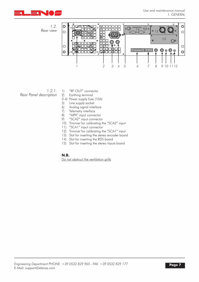
PS Messages:
The “PS Messages” section shows 8 zones, each of which comprises the following fields:
1-8 keys to select the window for modifying the contents of the corresponding PS mes-sage.
START text box corresponding to the time of start of transmission of the PS message. This field can only be modified if the OR key is lit.
STOP text box corresponding to the time of the end of transmission of the PS message. This field can only be modified if the OR key is lit.
ATT (active) key enabling the PS message to be transmitted on-air; if green, the mes-sage is on-air.
OR (time) key enabling the on-air message to be timed; if OR and ATT are both green, the PS message will go on-air between the times specified by the START and STOP fields.
SC (scroll) key enabling the transmission of the PS message in scrolling mode (one letter to the right every second).
ON indicator (green) confirming that the corresponding message is on-air.
3.4.10.RDS Encoder
Programming
Active messages (ATT lit green) which are not timed (OR grey) will be transmitted consecutively during intervals when timed messages are inactive. To ensure that the video programming is in step with the encoder, press the “Update” key.
Procedure for programming message 1
Press OR (time) so that it is lit green (time setting enabled)
Click the mouse on the START window Delete the previous time (CANC key) Enter the start time (using the same format:”XX:XX”)
Click the mouse on the STOP window Delete the previous time (CANC key) Write the end time of the message Press key 1 (the message programming window will appear)

Use and maintenance manual
Page 30 Engineering Department PHONE: +39 0532 829 965 - FAX: +39 0532 829 177E-Mail: [email protected]
3. USER INSTRUCTIONS
3.4.10.RDS Encoder Programming
Programming PS Messages
Having pressed one of the keys 1-8, corresponding to the number of the PS mes-sage to program, a window will appear with 16 fields for the words which make up the message, and the corresponding times for which the words will be displayed. The times, in seconds, can be programmed from a minimum of 1 second to a maximum of 60 seconds and represent the time for which the word will be displayed before being replaced by the next word. However, if the message is programmed to scroll (the SC key is lit green in the previous window), the times displayed have no relevance.
N.B.The fields which are left blank are not transmitted even if a display time of more than one second has been set.
Procedure for programming a message1. Double click on the text box where a word is to be entered, and then enter the word2. Adjust the display time of the word using the UP and DOWN arrows underneath the text box3. Repeat steps 1 and 2 for all the other words to be programmed4. Press the UPDATE key to save the message and exit from the window
Alternatively, press the EXIT key to exit from the window without saving the message
From the main window:
5. Press the ATT key (activate the message)6. Press the UPDATE key to update (the green ON indicator will light to show the message is active)7. It is now possible to insert other messages (upto 8) following the same procedure

Use and maintenance manual
Page 31Engineering Department PHONE: +39 0532 829 965 - FAX: +39 0532 829 177E-Mail: [email protected]
3. USER INSTRUCTIONS
3.4.10.RDS Encoder Programming
Alternative frequencies
The Alternative frequencies section allows 16 lists of different frequencies to be programmed, each in mode A or B. 8 lists are displayed at a time and with each one, the mode (A or B) with which it was programmed, the header frequency (this field is filled only if mode B has been used) and the number of frequencies in the list. To access a list just click the corresponding key with the mouse; a display will appear showing the mode and the list of possible frequencies on the left, and the frequencies in the list on the right. Double-click on a frequency contained in the left-hand list and it will be added, if not already present, to the list on the right. With mode A, it is possible to create a list with a maximum of 25 frequencies compared with 12 in mode B.
Method A/B
The EBU standard allows for the possibility of transmitting the set of frequencies to a network of transmitters in two modes, A and B.- Method A allows transmission of one or more lists of frequencies, each upto a maximum of 25.- Method B allows transmission of as many lists as there are transmitters in the network Each list is headed with the frequency of the transmitter to which it corresponds and contains all the frequencies of adjacent transmitters. Each receiver is designed to store a certain number of alternative frequencies which will be searched automatically for a new frequency when the current signal is too weak to receive. The search is as fast as the list of alternative frequencies is short. When the number of transmitters exceeds 12, it is advisable to use method B in which the rece-iver stores only the list corresponding to the header frequency to which it is tuned, so facilitating a faster change of frequency.

Use and maintenance manual
Page 32 Engineering Department PHONE: +39 0532 829 965 - FAX: +39 0532 829 177E-Mail: [email protected]
3. USER INSTRUCTIONS
Metodo A Metodo B
Esempi
3.4.10.RDS Encoder Programming
Programming alternative frequencies
To correctly program alternative frequencies, follow the instructions in sequence:
1. From the main menu, click on the key corresponding to the list to program. 2. Select method A or B. 3. Scroll the list of frequencies and double-click the mouse on the desired frequency. The data will be inserted in the selected list of frequencies (right- hand list). With method B selected, the first selected frequency is the header frequency and appears in the relevant window. To delete any stored fre- quency, double-click on it with the mouse. 4. To save the selection, click on USCITA. 5. In the main menu a green indicator will appear to the left of the list being modified or programmed to show that data is being changed. Click the UPDATE key to store the new data in the RDS board.
At this point, further alternative frequencies may be programmed.
Program identification
In this section parameters specific to the broadcaster are programmed; Program Identification, Program Type, Decoder Identification, Traffic Announcement, Traffic Pro-gram and Music/Speech.

Use and maintenance manual
Page 33Engineering Department PHONE: +39 0532 829 965 - FAX: +39 0532 829 177E-Mail: [email protected]
3. USER INSTRUCTIONS
3.4.10.RDS Encoder Programming
Program identification PI
PI is an identification code comprising 3 fields: COUNTRY + DIFFUSIONE + CODE. COUNTRY is a numerical value from 0 to 15 (0,F in hexadecimal) which identi-fies the country of the broadcaster (Italy - code 5). DIFFUSIONE is a numerical value from 0 to 15 (0,F in hexadecimal) which iden-tifies the area of coverage of the broadcast signal (local, regional, national, internatio-nal). CODE is a numerical value from 0 to 255 (00,FF in hexadecimal) which identi-fies the broadcaster; the code is assigned by an authorised organisation.
1. To program PI just click on the corresponding key with the mouse.2. Double-clicking on the item will automatically enable the relevant codes.3. Press the CONFIRM key to confirm the choice.4. To exit without saving, press CANCEL
Program Type and Decoder Identification DI
PTY is a code with 32 values (from 0 to 31) which identifies the type of transmis-sion being broadcast. DI identifies 16 different operational modes that the broadcaster can use.
- Click the PTY key with the mouse to start program-ming- To store the selection, press UPDATE.- To exit without saving, press EXIT.
Use and maintenance manual
Page 34 Engineering Department PHONE: +39 0532 829 965 - FAX: +39 0532 829 177E-Mail: [email protected]
3. USER INSTRUCTIONS
3.4.10.RDS Encoder Programming
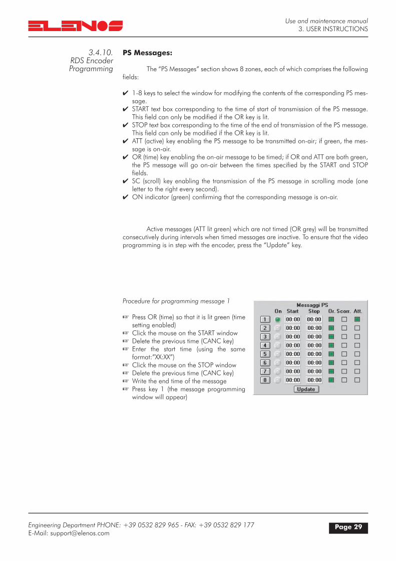
TA-TP-MS
At any time during the day, the broadcaster can interrupt the programme being transmitted with traffic news; for this reason the standard provides for a number of flags which indicate to the receiver that this information is being transmitted so that automatic tuning and/or volume adjustment can be made. These flags are named TA, TP and MS.
The TP flag identifies the broadcaster which is making traffic announcements The TA defines the time intervals between traffic announcements. The MS flag indicates whether the transmission is of Music or Speech (Voice)
These flags can be set by clicking the mouse on the relevant keys or via a remote keyboard connected to the appropriate board connector. If the remote keyboard is con-nected, the “Remote” key will be lit green and setup via a PC will be inhibited. If the colour of the TA, TP and MS keys do not agree with the encoder leds immediately above, this means that the flags set on the screen do not match those of the encoder. To update them press the Update key.
Radio Text
Radio Text is a message with a maximum length of 64 characters used to check the quality of the signal within the coverage area. The message is transmitted indefinitely
To program the message, click the mouse on the RTEXT key.To activate the message, click the mouse on the adjacent ON/OFF key.

Use and maintenance manual
Page 35Engineering Department PHONE: +39 0532 829 965 - FAX: +39 0532 829 177E-Mail: [email protected]
3. USER INSTRUCTIONS
3.4.10.RDS Encoder
Programming
EON Message
The EON message is used when a broadcaster has an agreement with another broadcaster (that we shall call “Friend”) to permit automatic tuning of receivers to Radio Friend, in areas where the signal quality of the broadcaster is poor or absent, or when Radio Friend is broadcasting information of interest to the listener. RDS allows programming of data upto a maximum of 8 partner broadcasters. Each broadcast network is a broadcaster in its own right and must therefore have unique identification of its data and allow all common services of interest identifiable between the two broadcasters.
Programming access to all this data is enabled by clicking the EON key located on the left side of the main panel; this displays the list of 8 networks that can be programmed.
Having chosen a network, a screen is displayed which shows all the parameters to be programmed: PI-PS-TA-TP-PTY-AF-PIN
PI is the identification code of radio Friend. PS is the 8 character message which is displayed on receivers tuned to the radio Friend frequencies.
TP indicates that the Friend broadcaster is enabled to transmit traffic news. TA indicates that the Friend broadcaster is transmitting traffic announcements. PTY indicates the type of programme. AF indicates the list of alternative frequencies on which radio Friend can be received.

Use and maintenance manual
Page 36 Engineering Department PHONE: +39 0532 829 965 - FAX: +39 0532 829 177E-Mail: [email protected]
3. USER INSTRUCTIONS
3.4.10.RDS Encoder Programming
The method of programming is similar to that of the main broadcaster (see pre-vious pages). For each network it is possible to program a maximum of 7 frequencies with method A and 4 frequencies with method B. To enable transmission of the programmed data for each network, just press the “Message Active” key; if it is coloured green, this means that the data is valid and may be transmitted.
ATTENTION: data relating to active networks (those for which the “Message Active” is green) are transmitted even if the ON/OFF key on the main panel is set (green).
Time & Clock Data
The RDS encoder has an on-board clock-calendar which provides an autono-mous timing function. The clock-calendar can be read and updated so that listener’s receivers can be synchronised. When this message is transmitted, the encoder sends a data packet containing the date and time referred to the Greenwich meridian on every change of minute. The time difference is expressed in half-hour steps.
To synchronise the clock-calendar to the actual date and time:
1. Press the CLOCK key or the TIME&C key

Use and maintenance manual
Page 37Engineering Department PHONE: +39 0532 829 965 - FAX: +39 0532 829 177E-Mail: [email protected]
3. USER INSTRUCTIONS
3.4.10.RDS Encoder Programming
2. Double-click on the TARGET TIME box and enter the time local to where the broadca-ster is transmitting.3. Double click on the TARGET DATE box and enter the date.4. Select the location with respect to Greenwich (the RDS system is able to update the time according to the country in which it is transmitting).5. Press the UPDATE key to transfer the data to the encoder.
If the EXIT key is pressed, the clock-calendar will not be changed.
Once the programming is complete, the PC can be diconnected and used for other pur-poses. Clicking the mouse on the EXIT key will terminate programming of the encoder.

Use and maintenance manual
Page 38 Engineering Department PHONE: +39 0532 829 965 - FAX: +39 0532 829 177E-Mail: [email protected]
3. USER INSTRUCTIONS
3.4.10.RDS Encoder Programming
Technical data
RDS SIGNAL ......................... as per CENELEC EN50067 ....................................... ENCODING......................... 2 level differential ..................................................... MODULATION ..................... DSB suppressed carrier ............................................. FREQUENCY........................ 57 KHz .................................................................... BAND .................................. +/- 2.4 KHz ............................................................
INPUT MPX........................... 0/+12 dBm into 600 Ohms ..................................... OUTPUT .............................. MPX+RDS ............................................................... MPX OUTPUT LEVEL.............. Inp. MPX.................................................................. RDS OUTPUT LEVEL .............. 20 - 150 mV RMS .................................................... OUTPUT IMPEDANCE........... 100 Ohms...............................................................
PS MESSAGES ...................... 8 with 16 words of 8 characters.................................
ALTERNATIVE ......................... 16 with maximum 250 frequencies each .................... FREQUENCY LISTS
MESSAGE............................. With IBM compatibile PC .......................................... PROGRAMMING
CONNECTION .................... RS232-C Standard ................................................... COMMUNICATION.............. Full Duplex............................................................... SPEED .................................. 2400 baud .............................................................. CONNECTORS .................... 9 Pin Cannon Female ........................................................................................... 9 Pin Cannon Male .............................................................................................. BNC........................................................................
MESSAGE MANAGEMENT .... Microcontroller.........................................................
DATA BACKUP ...................... 10 years ..................................................................
OPERATING TEMPERATURE... 0 - 55 °C................................................................. POWER SUPPLY .................... +12Vdc 100mA, +5Vdc 800mA ..............................

Use and maintenance manual
Page 39Engineering Department PHONE: +39 0532 829 965 - FAX: +39 0532 829 177E-Mail: [email protected]
3. USER INSTRUCTIONS
3.5.Checking performance
Power developed Connect a high quality wattmeter (e.g. Bird mod. 43) to the unit, via a double, male N-type connector. The wattmeter output is connected to a high quality dummy load (SWR less than 1.05) capable of dissipating at least 500W continuously via a 50 Ohm coaxial cable of appropriate cross section (e.g. RG213). Adjust the maximum range of the watt-meter to correspond to the power generated (e.g. for a Bird mod. 43 wattmeter, use a 500W probe adjusted to measure direct power). Power up the unit and check that the power shown on the display corresponds to the power displayed by the wattmeter. There is a tolerance of upto 25W difference between the two.It is of the utmost importance to use a wattmeter that is performing to its high precision specification.The measurement will be invalid if the wattmeter is connected to the unit via a coaxial cable without the double connector as specified.
Connect the unit to a dummy load with a -30dB output capable of dissipating at least 500W of continuous power, via a 50 Ohm coaxial cable of appropriate section (e.g. RG213). Connect the output of the dummy load, attenuted by another 20dB, to a fre-quency meter which is known to be performing to its high-precision specification. Power up the unit and check that the frequency shown on the display corresponds to the fre-quency displayed by the frequency meter. There is a tolerance of upto 100Hz difference between the two readings.
Connect the unit to a dummy load with a -30dB output capable of dissipating at least 500W of continuous power, with a coaxial cable of appropriate section (e.g. RG213). Connect the output of the dummy load, attenuated by another 20dB to a modulation analyser which is known to be performing to its high-precision specification. Connect the MPX input to a 1KHz sinusoidal signal from a low-frequency signal generator, with the amplitude adjusted for a level of 0dBm. Power up the unit and check that the deviation displayed by the unit and by the modulation analyser fall within the range 75KHz -0.2dB and 75 KHz.
Programmed frequency
Deviation
This procedure for checking performance should be carried out if there is any doubt over the integrity of the unit or possible damage sustained during transport. It should be performed by expert personnel capable of operating radiofrequency measure-ment equipment. The unit is calibrated using an FMAB modulation analyser (R&S) and so the per-formance checking equipment must be high precision, analogue instrumentation.

Use and maintenance manual
Page 40 Engineering Department PHONE: +39 0532 829 965 - FAX: +39 0532 829 177E-Mail: [email protected]
3. USER INSTRUCTIONS

Use and maintenance manual
Page 41Engineering Department PHONE: +39 0532 829 965 - FAX: +39 0532 829 177E-Mail: [email protected]
4. GENERAL DESCRIPTION
1
1
1
2
4.1.Introduction
This technical manual contains information regarding the operation, use and maintenance of the ETG250 (ETG300) exciter. The ETG250 (ETG300) operates in the frequency band from 87.5MHz to 108MHz in steps of 10KHz and is capable of developing a maximum, continuous power of 250W (300W).All the operating controls of the unit are directly accessible from the front panel whilst all the connectors are available on the rear panel.The connectors for measurement of signals are however located on the front panel.The exciter can be used for monophonic, stereo and composite multiplex transmissions. The ETG250 (ETG300) exciter is available in two versions which are identical from an operational point of view but have different power supply circuitry.
4.2.Using the
block diagram
The block diagrams describing the two versions of the ETG250 (ETG300) exciter are on the following two pages. The principle of communication between the various boards is clear from their interconnection; each connection is identified by a progressive number within a circle. In the pages following the block diagram where individual boards are decribed, the cable loom numbers are identified in order to simplify maintenance and eventual repair.
In this case, for example, the board is connected to the keyboard via flat 3, and the transformer is con-nected to the relay via cable 2 etc.In the board descriptions following the block dia-gram, the following information appears:
Connections:- 1 (JD1) via cable flat 3 to 1 (J1) of the monoboard
The first number is a reference whilst the number in brackets represents the name of the connector of the board in question.For more detail, see the layouts of the schematics.

Use and maintenance manual
Page 42 Engineering Department PHONE: +39 0532 829 965 - FAX: +39 0532 829 177E-Mail: [email protected]
4. GENERAL DESCRIPTION

Pag 1 file A3


Pag 2 file A3


Use and maintenance manual
Page 47Engineering Department PHONE: +39 0532 829 965 - FAX: +39 0532 829 177E-Mail: [email protected]
4. GENERAL DESCRIPTION
PD4
PD3
PD2
PD1
SCR1
C13C11
C26
C23 C28
U2
U1
U5 Q
1
Q2
C8
C7
C2
C4
C3
D6
C21
C20
R1 C9
D4
R3
R2
C15
R4
R5
D5
C16
C18
U4C17
D3
Q2
U3
C12
C1
C22
D1
D2C
6C
5
P1
C14
CN
1C
N2
C10
C19
R7
PD
5
C24
C25 D7
U6
C27
CN
4
CN
3
ELE
NO
S E
TG
-019
9-A
LI.C
R6
+
+
+
+
+
+
+
+
+
+
1
2
3
POWER SUPPLY
2
3
1
4.4.Power supply section
The ETG250 (ETG300) uses a switch-mode converter in the transformer version and a switch-mode power supply connected direct to the line supply in the other version (DR).The section which supplies power to the services is the same for both versions.The ETG250 (ETG300) exciter features, on both versions, a line filter fitted to the alterna-ting supply to provide maximum suppression of conducted interference.The use of discrete component technology enables easy replacement in the event of fai-lure.
4.4.1.Service power supply
The service (or auxiliary) power supply furnishes 5 separate supplies which supply the various boards which go to make up the unit. The table below summarises the supply voltages for each section of the unit and the corresponding protection. The service (or auxiliary) power supply is a linear type in order to reduce to a minimum any disturbances that could interfere with the boards.
Connections:- 1 (CN1) via cable 13 to 2 to the “DRIVER” board- 2 (CN2) via cable 4 to 1 (J1) of the mother board- 3 (CN3) via cable 7 to the transformer
4.4.2.Switch-mode power supply (DR version)
Supplies a variable voltage from +30V to +50V, with current and voltage protection.It uses a mix of SMD and traditional technology to reduce the space occupied as far as possible. The power supply features thermal protection and a further line filter equipped with VDRs on the input.
Connections:(only in the switch-mode DR version)- 1 via cable 2 to the relay- 2 via cable 5 to 1 (J1) of the mother board- 3 via cable 18 to 3 of the RF modules
Supply Voltage
+12V
-12V
+5V
+12VRF
+18VRF
Boards supplied
Mother board(CPU, PLL, BUS)
Mother board(CPU, PLL, BUS)
Mother board(CPU, PLL, BUS)
RF driver stage
RF driver stage
Protection
Current protection
Current protection
Current and voltage pro-tection
Current protection
Current protection

Use and maintenance manual
Page 48 Engineering Department PHONE: +39 0532 829 965 - FAX: +39 0532 829 177E-Mail: [email protected]
4. GENERAL DESCRIPTION
1
2 3
E-ATG10-98-1.1
+
+
C8
C3
R13
C30
C23
C12 R5
L7L8
Q2
C5 R14
C16
C17
C19
L11
L6
L4
R8
C20
L10
C25
C24
R18
R6R15
R7
R2 R3
C13
C1
R12
R16L1
C26 C22C27 C21
L9
R19
L3C11
R4C15
C14
C6
R1
P1R10
R11
Q1
C2
C9
L2
R9
U1
1
2
3
4.4.2.2.Transformer power
supply
Supplies a variable voltage from +20V to +50V with voltage and current protection.Uses traditional technology to facilitate replacement of faulty parts.The power supply also features thermal protection and both input and output filters in order to minimise interference.
Connections:(Only for the transformer version)- 1 via cable 5 to 1 (J1) of the mother board- 2 via cable 18 to 3 of the RF modules- 3 via cable 19 to 1 (J1) of the mother board
4.5.Radiofrequency
section
The driver comprises an input stage of about 10mW and supplies a maximum output power of 15W. It is built using a mix of technologies and subdivided into three main amplifying stages. The first stage is a “MMIC” type “ERA5”. The second stage is a MOS BLF404. The third stage is a MOS BLF244. The output of the driver is connected to the input splitter.
Connections:- 1 via coaxial cable 10 to 3 (J8 RF OUT) of the mother board- 2 via cable 13 to 1 (CN1) of the services power supply (auxiliary)- 3 via coaxial cable 14 to 1 of the input splitter (Splitter IN)
4.5.1.Driver
This comprises a low power output stage (driver) which, via a splitter, supplies the power to the two final power stages. The power output from the modules supplies a coupler (or output adder) which concentrates all the power to the input of the low-pass filter. The measurement probe which is located on the final part of the low-pass filter, reads the values of direct and reflected power for the CPU.

Use and maintenance manual
Page 49Engineering Department PHONE: +39 0532 829 965 - FAX: +39 0532 829 177E-Mail: [email protected]
4. GENERAL DESCRIPTION
4
2PC
B02
52_1
C1
TF1
R7
U1
P1C5
C6
C4D1
C9C10
C2
C3R1
L2
R9C13
C12C11C15
C14
C18C19 C16
C17
L1
R8
25 Ohm25 Ohm
50 Ohm
C7C8
R6
R2R3
R4R5
+
1
2
3
1
1
2
RF Out
4.5.2.RF Modules
The two modules comprise a MOSFET (BLF278) and are capable of delivering a maximum power of 300W each. The gates are controlled by the CPU so that power output can be inhibited when the user changes frequency. The outputs of both modules enter the couple (or output combiner).
Connections:- 1 via coaxial cables 15 and 16 to 2 and 3 of the input splitter (Splitter IN)- 2 via cable 6 to 1 (J1) of the mother board- 3 via cable 18 to 2 of the power supply (this is dependant on the version of power supply)- 4 via coaxial cable 17 to 2 of the low-pass filter (LPF INPUT)
4.5.3.Low-pass filter
This is a ninth order “CHEBYCHEV” filter, with teflon support. It guarantees the suppression of harmonic components with the limits set by International standards.
Connections:- 1 (JP1) via flat cable to 5 (CN1) of the mother board- 2 via coaxial cable 17 to 4 of the RF Modules
“RF Out” indicates the RF power output connector which is located on the rear panel
4.5.4.1.Directional coupler
Output power measurement
The directional coupler is located on the final output stage of the low-pass filter. It is designed using SMD technology and is shielded to prevent RF intereference. It generates a voltage proportional to the direct and reflected power.
Connections:- 1 (JP1) via flat cable 11 to 5 (CN1) of the mother board
N.B.The directional coupler is mounted on the same circuit board.
4.5.4.2.Directional coupler
AGC protection
A control circuit regulates the output power and maintains it to within +0.1dB across the whole operating band, progressively reducing it down to 50W in the event of excessive SWR. This enables the exciter to continue to work with infinite SWR at any phase angle.

Use and maintenance manual
Page 50 Engineering Department PHONE: +39 0532 829 965 - FAX: +39 0532 829 177E-Mail: [email protected]
4. GENERAL DESCRIPTION
1 2 3
4
5
1
2 3
4.6.Logic
(Mother board)
This board is constructed using only SMD technology and comprises the fol-lowing stages:- CPU- AGC- VCO/PLL- MPX
Connections:- 1 (J1) via cable 4 to 2 (CN2) of the services (auxiliary) power supply - 1 (J1) via cable 5 to 1 of the power supply (dependant on the version)- 1 (J1) via cable 6 to 2 of the RF Modules- 2 (JD1) via cable flat to 1 (JD1) of the Keyboard- 3 (SC1) via coaxial cable 10 to 1 of the Driver- 4 (CN2) via cable 12 to the temperature sensor- 5 (CN1) via cable flat 11 to 1 of the directional coupler
4.6.1.CPU
The CPU controls the display, the keyboard, ALC and the VCO/PLL. It comprises an 80C552 microprocessor which operates at a clock rate of 16MHz. It features a 256 Kbit RAM and a 2Mbit ROM. It receives input signals from the directional coupler and supplies processed signals to the ALC. It also controls all the audio functions.
4.6.2.ALC
This receives signals from the CPU and supplies 2 output voltages:1) Controls the MOS gates2) Controls the output voltage of the power supply. It features SWR protection which limits the output power in the event of an SWR in excess of the programmed threshold.
4.6.3.VCO/PLL
The PLL board generates the frequency-modulated RF signal using phase-lock synthesis. The oscillator, controlled by the VCO voltage and mounted next to the PLL board, uses very low-noise components and also separation stages to obtain very low phase noise. The reference frequency is generated by a temperature-compensated oscillator with a maximum drift of 1ppm.
4.7.Keyboard
This is interfaced to the CPU and supplies signals to the display as well as power for illumination. A trimmer allows adjustment of the contrast. 8 soft keys perform functions shown on the display.
Connections:- 1 (JP1) via flat cable 3 to 2 (JD1) of the mother board- 2 via cable 8 to the display- 3 (JD1) via flat cable 9 to the display
4.6.4.MPX
Accepts the wide-band MPX input signal, i.e. it supplies the transmitter with a stereo signal derived from an external stereo encoder. It features 2 SCA inputs, one of which can be used as an RDS data input. The two unbalanced inputs for SCA signals accept input frequencies upto 200 KHz. The MPX also supplies the microcontroller with an appropriately processed MPX signal so that the level can be displayed as a bar graph and in dBV values. The inputs are protected against over-voltage.The inputs are unbalanced on BNC connectors (impedance 10KOhm).
Use and maintenance manual
Page 51Engineering Department PHONE: +39 0532 829 965 - FAX: +39 0532 829 177E-Mail: [email protected]
4. GENERAL DESCRIPTION
2 13
2 13
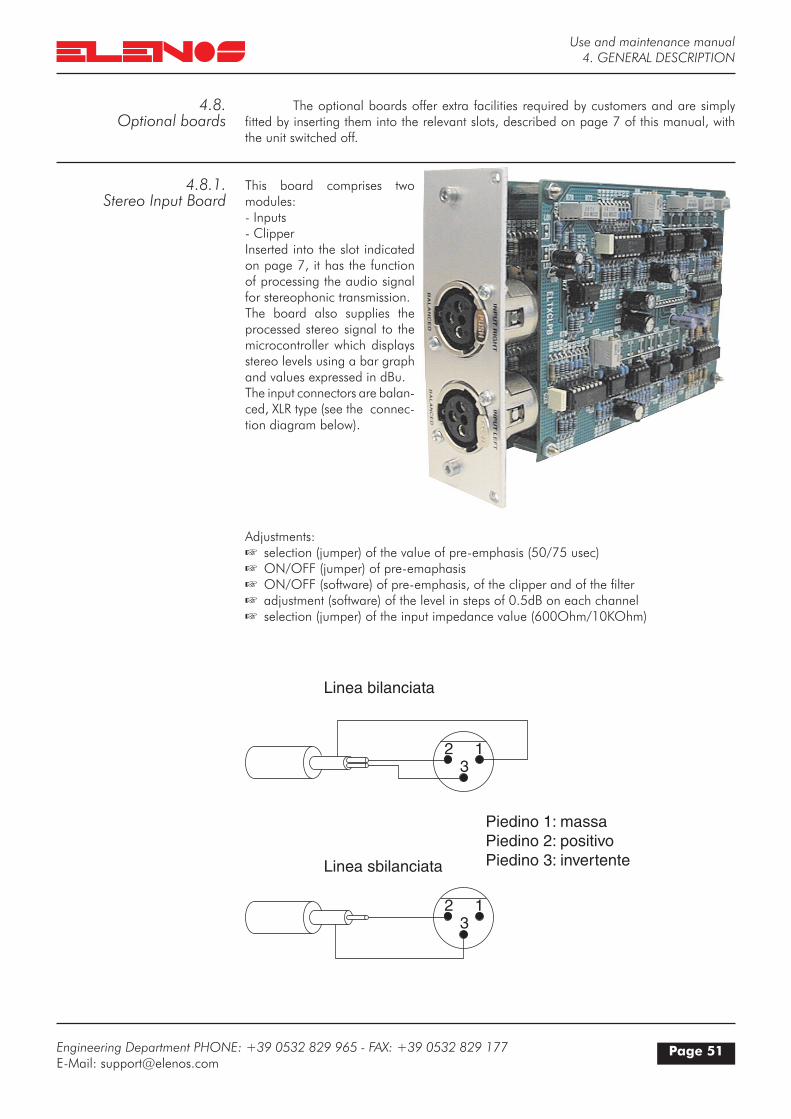
Linea bilanciata
Linea sbilanciata
Piedino 1: massaPiedino 2: positivoPiedino 3: invertente
4.8.Optional boards
4.8.1. Stereo Input Board
The optional boards offer extra facilities required by customers and are simply fitted by inserting them into the relevant slots, described on page 7 of this manual, with the unit switched off.
This board comprises two modules:- Inputs- ClipperInserted into the slot indicated on page 7, it has the function of processing the audio signal for stereophonic transmission.The board also supplies the processed stereo signal to the microcontroller which displays stereo levels using a bar graph and values expressed in dBu.The input connectors are balan-ced, XLR type (see the connec-tion diagram below).
Adjustments: selection (jumper) of the value of pre-emphasis (50/75 usec) ON/OFF (jumper) of pre-emaphasis ON/OFF (software) of pre-emphasis, of the clipper and of the filter adjustment (software) of the level in steps of 0.5dB on each channel selection (jumper) of the input impedance value (600Ohm/10KOhm)
Use and maintenance manual
Page 52 Engineering Department PHONE: +39 0532 829 965 - FAX: +39 0532 829 177E-Mail: [email protected]
4. GENERAL DESCRIPTION
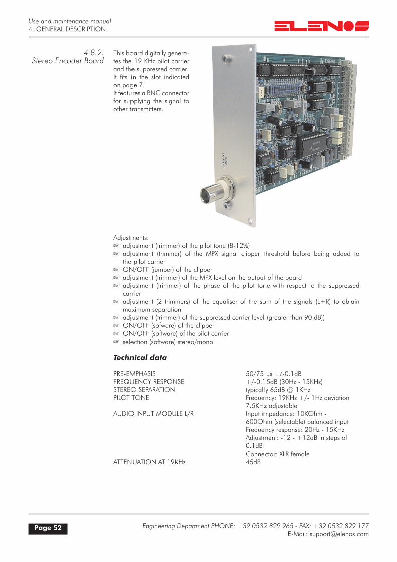
4.8.2.Stereo Encoder Board
This board digitally genera-tes the 19 KHz pilot carrier and the suppressed carrier.It fits in the slot indicated on page 7.It features a BNC connector for supplying the signal to other transmitters.
Adjustments: adjustment (trimmer) of the pilot tone (8-12%) adjustment (trimmer) of the MPX signal clipper threshold before being added to
the pilot carrier ON/OFF (jumper) of the clipper adjustment (trimmer) of the MPX level on the output of the board adjustment (trimmer) of the phase of the pilot tone with respect to the suppressed
carrier adjustment (2 trimmers) of the equaliser of the sum of the signals (L+R) to obtain
maximum separation adjustment (trimmer) of the suppressed carrier level (greater than 90 dB)) ON/OFF (sofware) of the clipper ON/OFF (software) of the pilot carrier selection (software) stereo/mono
Technical data
PRE-EMPHASIS 50/75 us +/-0.1dBFREQUENCY RESPONSE +/-0.15dB (30Hz - 15KHz) STEREO SEPARATION typically 65dB @ 1KHz PILOT TONE Frequency: 19KHz +/- 1Hz deviation 7.5KHz adjustableAUDIO INPUT MODULE L/R Input impedance: 10KOhm - 600Ohm (selectable) balanced input Frequency response: 20Hz - 15KHz Adjustment: -12 - +12dB in steps of 0.1dB Connector: XLR femaleATTENUATION AT 19KHz 45dB

Use and maintenance manual
Page 53Engineering Department PHONE: +39 0532 829 965 - FAX: +39 0532 829 177E-Mail: [email protected]
4. GENERAL DESCRIPTION
4.8.3. RDS Board
Introduction
For several years now, within the field of radio broadcasting, the importance of transmitting data packets of various types, over and above the radio signal, has been recognised as crucial to improving the quality and reliability of the services offered, let alone implementing new ones. This need was acknowledged at international level and a study group was given a mandate to identify the various needs and define a transmission standard which is suitable for the sector. The group created the RADIO DATA SYSTEM (RDS) which is now the most diffuse system of data transmission in the radiophonic sector. The optional RDS board fits in the slot indicated on page 7 of this technical manual. The ETG250 (ETG300)’s optional RDS board allows a data channel to be tran-smitted alongside the radiophonic signal (mono or stereo), in conformity with the “Speci-fication of the radio data system (RDS)” document, published by the European Committe for Electrotechnical Standardization (CENELEC) Ref. NO. EN50067:1990.
RDS system
The RADIO-DATA-SYSTEM (RDS) has been specified for the transmission of infor-mation within mono/stereophonic programmes in the VHF/MF (87.5-108MHz) band, thus satisfying the requirements for transmission of additional data in radiophonic pro-grammes.
> Compatibility with actual mono/stereophonic programmes> Absence of intereference between adjacent channels> Compatibility with other existing systems of identification

Use and maintenance manual
Page 54 Engineering Department PHONE: +39 0532 829 965 - FAX: +39 0532 829 177E-Mail: [email protected]
4. GENERAL DESCRIPTION
The system, selected by an international working group of specialists, allows data transmission at a speed of 1187.5 bit/sec with phase modulation at two levels, 57KHz carrier and band +/- 2KHz. The transmitted binary signal undergoes differential enco-ding. The transmission protocol comprises packets of 104 bit (87.6ms) length, named GROUPS, each comprising 4 BLOCKS of 26 bits each. Each BLOCK is made up of 16 bits of information and 10 protection bits, designed specifically to allow words to be cor-rected upto a maximum of 5 bit in error. 16 distinct GROUPS are provided, some of which have not yet been defined. Each group starts with an identification code (PI) which has the double scope of synchronising the receiver and identifying the broadcaster that is transmitting the signal. The PI comprises a 4 bit code to identify the country (Italy is code 5), a 4 bit code to define the coverage of the transmitted signal (International, National, Sub-National,Regional or Local) and an 8 bit code for the number of reference of the program. The Zero GROUP is used for sending the PS message (shown on the display of RDS compatible receivers) and for tuning frequencies. Each Zero group contains 2 cha-racters of the message, two tuning frequencies, a code which defines the type of transmis-sion (mono, stereo, compressed, etc.), a bit to define whether music or speech is being transmitted and a code for signalling the transmission of traffic news. Two formats are provided for the transmission of alternative frequencies:A) Each station transmits a unique list of frequencies, preceded by the number of frequen-cies that it contains (max 25);B) Each station transmits a unique list of frequencies for each transmitter that it possesses. The list begins with the header frequency, followed by the frequencies (max 12) used by adjacent transmitters in the coverage area. This method is more efficient when the list of frequencies is long because it presents the self-tuning system with fewer frequencies to choose from and thus speed up the process of searching for new frequencies. If the number of frequencies is low, mode A is advised as it requires less data to be transmit-ted.
4.8.3.RDS board
RDS system
The RDS encoder comprises a single Euro card offe-ring the following features:
Connector 41612 which accepts the power supply volta-ges +5V and +12V
BNC for the input of the mono or stereo signal BNC for the ouptput of the MPX signal and/or MPX+RDS Cannon connector 9 PIN for serial connection to a PC Cannon connector 9 PIN for connection of a remote key-board
A panel-mounted trimmer for adjusting the RDS signal level
Led indicator, for lock and carrier generation RDS (LOCK) Led indicator, for synchronisation with stereo carrier (STEREO)
Led indicator for remote control active (REM) Led indicator for TP set (TP) Led indicator for TA set (TA) Led indicator for MS set (MS

Use and maintenance manual
Page 55Engineering Department PHONE: +39 0532 829 965 - FAX: +39 0532 829 177E-Mail: [email protected]
4. GENERAL DESCRIPTION
1 DCD2 RxD3 TxD4 DTR5 GND6 DSR7 RTS8 CTS9 RI
DCD 1RxD 2TxD 3DTR 4GND 5DSR 6RTS 7CTS 8
RI 9
12 TxD3 RxD4 RTS5 CTS6 DSR7 SG8 DCD9......1920 DTR21......25
DCD 1RxD 2TxD 3DTR 4GND 5DSR 6RTS 7CTS 8
RI 9
DB25 Female - DB9 Male
DB9 Female - DB9 Male
4.8.3.RDS board
The board is equipped with DB25-type female to DB9-type male cable, which can be replaced by a DB9 female to DB9 male cable (see diagram below), plus a 3.5” floppy with software for correctly programming the RDS.
N.B.The software supplied is Microsoft Windows (c) compatible.
The board features a microcontroller which controls the RDS message genera-tion. The services supported by the encoder are programmed via a PC connected to the serial interface, running an easy-to-use program. Once programmed, the RDS mes-sages are saved, even in the absence of primary power. The board is equipped with a timer-calendar which updates the date and time even when no external power is present. The RDS carrier is generated internally by a quartz oscillator, but when a 19KHz carrier is applied to the MPX1 IN input, whose amplitude, stability and frequency conform with the specification, the encoder locks to the external frequency and generates the 57 KHz synchronised to it (STEREO led lit). Thanks to the microcontroller, the encoder can modify the transmitted message in real time which makes the system extremely flexible and adaptable to the various customer requirements. The software supplied allows programming of a set of 8 distinct PS Messages each comprising 16 words of 8 characters and a maximum of 16 lists of alternative fre-quencies. These limits are not binding but have been advised by a sample of users.

Use and maintenance manual
Page 56 Engineering Department PHONE: +39 0532 829 965 - FAX: +39 0532 829 177E-Mail: [email protected]
4. GENERAL DESCRIPTION
The set of messages can be put on-air automatically at any hour of the day. Programming of the messages is very quick and easy; an entire message can be programmed in one minute. No special knowledge is necessary on the part of the user.
4.8.3.RDS board
Use and maintenance manual
Page 57Engineering Department PHONE: +39 0532 829 965 - FAX: +39 0532 829 177E-Mail: [email protected]
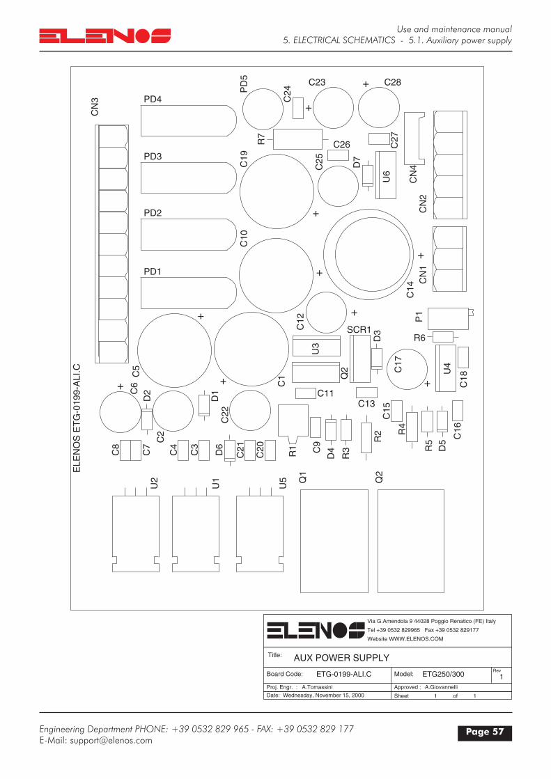
5. ELECTRICAL SCHEMATICS - 5.1. Auxiliary power supply
ETG250/300
A.GiovannelliA.Tomassini
ETG-0199-ALI.C
Wednesday, November 15, 2000 11
AUX POWER SUPPLY
1Model:
Approved :Proj. Engr. :
Website WWW.ELENOS.COM Tel +39 0532 829965 Fax +39 0532 829177 Via G.Amendola 9 44028 Poggio Renatico (FE) Italy
ofSheetDate:
RevBoard Code:
Title:
PD4
PD3
PD2
PD1
SCR1
C13C11
C26
C23 C28
U2
U1
U5 Q
1
Q2
C8
C7
C2
C4
C3
D6
C21
C20
R1 C9
D4
R3
R2
C15
R4
R5
D5
C16
C18
U4C17
D3
Q2
U3
C12
C1
C22
D1
D2C
6C
5
P1
C14
CN
1C
N2
C10
C19
R7
PD
5
C24
C25 D7
U6
C27
CN
4
CN
3
ELE
NO
S E
TG
-019
9-A
LI.C
R6
+
+
+
+
+
+
+
+
+
+

Use and maintenance manual
Page 58 Engineering Department PHONE: +39 0532 829 965 - FAX: +39 0532 829 177E-Mail: [email protected]
5. ELECTRICAL SCHEMATICS - 5.1. Auxiliary power supply

Pag 3 file A3


Use and maintenance manual
Page 61Engineering Department PHONE: +39 0532 829 965 - FAX: +39 0532 829 177E-Mail: [email protected]
5. ELECTRICAL SCHEMATICS - 5.1. Auxiliary power supply
Ref. DescriptionParts list
CN1 WIELAND 3 M V CN2 WIELAND 5 M V CN3 HEADER 11 CN4 AMP MODUII 4 M V C1 CEV 4700uF 35V C5 CEV 4700uF 35V C10 CEV 4700uF 35V C19 CEV 4700uF 35V C2 100nF 50V CER. C2 CEV 100uF 63V C6 CEV 100uF 63V C12 CEV 100uF 63V C17 CEV 100uF 63V C22 CEV 100uF 63V C3 CMY 0.1uF 63V C4 CMY 0.1uF 63V C7 CMY 0.1uF 63V C8 CMY 0.1uF 63V C9 CMY 0.1uF 63V C11 CMY 0.1uF 63V C13 CMY 0.1uF 63V C15 CMY 0.1uF 63V C16 CMY 0.1uF 63V C18 CMY 0.1uF 63V C20 CMY 0.1uF 63V C21 CMY 0.1uF 63V C14 CEV 2200uF 63V D1 DIODE 1N4007 D2 DIODE 1N4007 D4 DIODE 1N4007 D5 DIODE 1N4007 D6 DIODE 1N4007 D3 BZX85C5V6 HOL1 CONNECTOR SCREW HOL2 CONNECTOR SCREW HOL3 CONNECTOR SCREW HOL4 CONNECTOR SCREW PD1 BRIDGE KBU8K PD2 BRIDGE KBU8K PD3 BRIDGE KBU8K PD4 BRIDGE KBU8K P1 RES. 67X 10K Q1 BC337 Q1 TIP34C Q3 TIP34C Q2 BD140 R1 RES. 0.22R 5W 5% R1 22K 0.25W 5% R4 RES. 18R 0.5W 5% R2 RES. 18R 0.5W 5% R3 RES. 22R 0.25W 5% R5 RES. 1K 0.25W 5% R6 RES. 12K 0.25W 5% SCR1 TIC216M U1 LM7812CT

Use and maintenance manual
Page 62 Engineering Department PHONE: +39 0532 829 965 - FAX: +39 0532 829 177E-Mail: [email protected]
5. ELECTRICAL SCHEMATICS - 5.1. Auxiliary power supply
Ref. DescriptionParts list
U2 LM7912CT U3 LM7805CT U4 LM317 U5 UA7812

Use and maintenance manual
Page 63Engineering Department PHONE: +39 0532 829 965 - FAX: +39 0532 829 177E-Mail: [email protected]
5. ELECTRICAL SCHEMATICS - 5.2. Switching power supply
ETG250/300
A.GiovannelliA.Tomassini
E13-98AA-ALI.B
Wednesday, November 15, 2000 11
SWITCHING CONVERTER
1Model:
Approved :Proj. Engr. :
Website WWW.ELENOS.COM Tel +39 0532 829965 Fax +39 0532 829177 Via G.Amendola 9 44028 Poggio Renatico (FE) Italy
ofSheetDate:
RevBoard Code:
Title:

Use and maintenance manual
Page 64 Engineering Department PHONE: +39 0532 829 965 - FAX: +39 0532 829 177E-Mail: [email protected]
5. ELECTRICAL SCHEMATICS - 5.2. Switching power supply

Pag 4 file A3


Use and maintenance manual
Page 67Engineering Department PHONE: +39 0532 829 965 - FAX: +39 0532 829 177E-Mail: [email protected]
5. ELECTRICAL SCHEMATICS - 5.2. Switching power supply
Ref. DescriptionParts list
R1 4,7K Resistenza a filo cassa ceramica R2 39K Resistenza strato di carbone R3 30,1K Resistenza strato metallico R4 5,11K Resistenza strato metallico R5 6,8K Resistenza strato di carbone R6 4,7R Resistenza strato di carbone R7 10K Resistenza ossidi metallici R8 1K Resistenza strato di carbone R9 4,22K Resistenza strato metallico R10 150K Resistenza strato di carbone R11 8,2K Resistenza strato di carbone R12 3,3K Resistenza strato di carbone R13 15K Resistenza strato di carbone R14 8,2K Resistenza strato di carbone R15 1K Resistenza strato di carbone R16 2,7R Resistenza ossidi metallici R17 365K Resistenza strato metallico R18 10K Resistenza strato metallico R19 1K Resistenza strato di carbone R20 22K Resistenza strato di carbone R21 10K Resistenza strato metallico R22 1K Resistenza strato metallico R23 10K Resistenza strato di carbone R24 100R Resistenza strato metallico R25 500R Trimmer verticale multigiri R26 5K Trimmer verticale multigiri R27 4,22K Resistenza strato metallico R28 30,1K Resistenza strato metallico R29 4,7K Resistenza strato di carbone R30 R31 10K Resistenza strato di carbone R32 90,9K Resistenza strato metallico R33 10K Resistenza strato metallico R34 220R Resistenza strato di carbone R35 10R Resistenza strato di carbone R36 15R Resistenza ossidi metallici R37 4,7K Resistenza ossidi metallici R38 50K Trimmer verticale multigiri R39 10K Resistenza strato metallico R40 1K Resistenza strato metallico R41 1K Resistenza strato metallico R42 1,96K Resistenza strato metallico R43 226R Resistenza strato metallico R44 100R Resistenza strato di carbone R45 2,2K Resistenza strato di carbone R46 2,2K Resistenza strato di carbone R47 100K Resistenza strato di carbone R48 330R Resistenza strato di carbone R49 86,6K Resistenza strato metallico R50 4,22K Resistenza strato metallico TH1 Termistore PTC:PTH9M04BF222TS2F333 C1 1uF Cond. Poliestere scatolino C2 22nF Cond. Ceramico multistrato C3 22nF Cond. Ceramico multistrato C4 22nF Cond. Ceramico multistrato

Use and maintenance manual
Page 68 Engineering Department PHONE: +39 0532 829 965 - FAX: +39 0532 829 177E-Mail: [email protected]
5. ELECTRICAL SCHEMATICS - 5.2. Switching power supply
Ref. DescriptionParts list
C5 1uF Cond. Poliestere scatolino C6 47uF Cond. Elettrolitico verticale105° C7 1000uF Cond. Elettrolitico snap-in 85° C8 1000uF Cond. Elettrolitico snap-in 85° C9 1000uF Cond. Elettrolitico snap-in 85° C10 1uF Cond. Poliestere scatolino C11 100nF Cond. Ceramico multistrato C12 100nF Cond. Ceramico multistrato C13 1uF Cond. Ceramico multistrato C14 100nF Cond. Ceramico multistrato C15 1uF Cond. Ceramico multistrato C16 47uF Cond. Elettrolitico verticale C17 1uF Cond. Ceramico multistrato C18 330pF Cond. Ceramico multistrato C19 1nF Cond. Poliestere scatolino C20 10nF Cond. Ceramico multistrato C21 100nF Cond. Ceramico multistrato C22 10uF Cond. Tantalio a goccia C23 10pF Cond. Ceramico a disco C24 100nF Cond. Ceramico multistrato C25 100pF Cond. Ceramico multistrato C26 100nF Cond. Ceramico multistrato C27 1uF Cond. Ceramico multistrato C28 100nF Cond. Ceramico multistrato C29 100nF Cond. Ceramico multistrato C30 2,2nF Cond. Ceramico multistrato C31 100nF Cond. Ceramico multistrato C32 100nF Cond. Ceramico multistrato C33 2,2nF Cond. Ceramico alta tensione C34 1uF Cond. Poliestere scatolino C35 22uF Cond. Elettrolitico verticale 105° C36 220uF Cond. Elettrolitico verticale 105° C37 1uF Cond. Ceramico multistrato C38 100nF Cond. Ceramico multistrato C39 22nF Cond. Ceramico multistrato C40 22nF Cond. Ceramico multistrato C41 1uF Cond. Poliestere scatolino C42 C43 100nF Cond. Ceramico multistrato C44 1nF Cond. Ceramico multistrato C45 100nF Cond. Ceramico multistrato C46 100nF Cond. Ceramico multistrato C47 1uF Cond. Ceramico multistrato C48 100nF Cond. Ceramico multistrato C49 100nF Cond. Ceramico multistrato C50 220nF Cond. Ceramico multistrato C51 100nF Cond. Poliestere scatolino C52 330pF Cond. Ceramico multistrato C53 4,7nF Cond. Ceramico multistrato CX 1uF Cond. Poliestere scatolino D1 1N4148 Diodo silicio D2 ZPD5,6V Diodo zener D3 BAT48 Diodo schottky D4 BYV27-200 Fast recovery avalance diode D5 1N4148 Diodo silicio

Use and maintenance manual
Page 69Engineering Department PHONE: +39 0532 829 965 - FAX: +39 0532 829 177E-Mail: [email protected]
5. ELECTRICAL SCHEMATICS - 5.2. Switching power supply
Ref. DescriptionParts list
D6 BYV27-200 Fast recovery avalance diode D7 16CTQ100 Center-tape schottky diode D8 ZPD5,6V Diodo zener D9 BYV27-200 Diodo schottky D10 BYV27-200 Diodo schottky D11 BYV27-200 Diodo schottky D12 BYV27-200 Diodo schottky D13 DB3 Diodo diac D14 BZY97C24 Diodo zener Q1 BU406 Transistor NPN Q2 BC547B Transistor NPN Q3 BC547B Transistor NPN Q4 BC547B Transistor NPN Q5 BC337-25 Transistor NPN Q6 BC327-25 Transistor PNP Q7 BC327-25 Transistor PNP MX IRF3415 Powermos (47mOhm) SC1 MCR264 Thristor IC1 TL431-CLP Adjustable zener shunt regulator IC2 L4990 Current mode control PWM IC3 L6380 High-side driver IC4 LM358N Dual operation amplifier IC5 TL321C Operation amplifier IC6 LM317CT Adjustable regulator IC7 TL431-CLP Adjustable zener shunt regulator Z1 220uH Induttanza HF a scatolino Z2 220uH Induttanza HF a scatolino Z3 100uH Induttanza HF a scatolino Z4 2,2mH Induttanza HF a scatolino Z5 2,2mH Induttanza HF a scatolino CT TRI120-1 Current trasformer PI IN27V-1 Power inductor EM1 EMI360-1 EMI Filter EM2 EMI360-1 EMI Filter J1 AMPMODU II Connettore Maschio 2pin dritto J2 AMPMODU II Connettore Maschio 2pin dritto J3 AMPMODU II Connettore Maschio 2pin dritto J4 AMPMODU II Connettore Maschio 2pin dritto J5 AMPMODU II Connettore Maschio 2pin dritto FT1-9 DB9 Conn. A vasch. Filtrato 9pin Maschio FTA-D Filtro feed-through a bullone

Use and maintenance manual
Page 70 Engineering Department PHONE: +39 0532 829 965 - FAX: +39 0532 829 177E-Mail: [email protected]
5. ELECTRICAL SCHEMATICS - 5.2. Switching power supply

Pag 5 file A3Serigrafia monoscheda


Pag 6 file A3Schema VCO


Pag 7 file A3schema PLL


Pag 8 file A3Schema MPX


Pag 9 file A3Schema AGC


Pag 10 file A3Schema CPU


Use and maintenance manual
Page 83Engineering Department PHONE: +39 0532 829 965 - FAX: +39 0532 829 177E-Mail: [email protected]
5. ELECTRICAL SCHEMATICS - 5.3. Mother board
Ref. DescriptionParts list
CN1 HEADER 10 Connett. per flat cable 2X5 CN2 AMP MODU II Connett. AMP MODU 2pin p 2,54 CX1 47uF Cond. elettrolitico Case D C25 47uF Cond. elettrolitico Case D C30 47uF Cond. elettrolitico Case D C33 47uF Cond. elettrolitico Case D CX10 22uF 25V (montato volante) C1 1nF Cond. ceramico SMT 0805 C10 1nF Cond. ceramico SMT 0805 C11 1nF Cond. ceramico SMT 0805 C14 1nF Cond. ceramico SMT 0805 C18 1nF Cond. ceramico SMT 0805 C21 1nF Cond. ceramico SMT 0805 C22 1nF Cond. ceramico SMT 0805 C41 1nF Cond. ceramico SMT 0805 C139 1nF Cond. ceramico SMT 0805 C147 1nF Cond. ceramico SMT 0805 C149 1nF Cond. ceramico SMT 0805 C2 47uF Cond. tantalio Case 3528 C3 4.7nF Cond. ceramico SMT 0805 C5 4.7nF Cond. ceramico SMT 0805 C6 4.7nF Cond. ceramico SMT 0805 C9 4.7nF Cond. ceramico SMT 0805 C12 4.7nF Cond. ceramico SMT 0805 C13 4.7nF Cond. ceramico SMT 0805 C19 4.7nF Cond. ceramico SMT 0805 C23 4.7nF Cond. ceramico SMT 0805 C24 4.7nF Cond. ceramico SMT 0805 C26 4.7nF Cond. ceramico SMT 0805 C27 4.7nF Cond. ceramico SMT 0805 C28 4.7nF Cond. ceramico SMT 0805 C29 4.7nF Cond. ceramico SMT 0805 C31 4.7nF Cond. ceramico SMT 0805 C32 4.7nF Cond. ceramico SMT 0805 C34 4.7nF Cond. ceramico SMT 0805 C35 4.7nF Cond. ceramico SMT 0805 C40 4.7nF Cond. ceramico SMT 0805 C157 4.7nF Cond. ceramico SMT 0805 C158 4.7nF Cond. ceramico SMT 0805 C152 220nF Cond. ceramico SMT 0805 C4 220nF Cond. ceramico SMT 0805 C7 100nF Cond. ceramico SMT 0805 C15 100nF Cond. ceramico SMT 0805 C17 100nF Cond. ceramico SMT 0805 C20 100nF Cond. ceramico SMT 0805 C42 100nF Cond. ceramico SMT 0805 C43 100nF Cond. ceramico SMT 0805 C44 100nF Cond. ceramico SMT 0805 C45 100nF Cond. ceramico SMT 0805 C47 100nF Cond. ceramico SMT 0805 C49 100nF Cond. ceramico SMT 0805 C50 100nF Cond. ceramico SMT 0805 C51 100nF Cond. ceramico SMT 0805 C52 100nF Cond. ceramico SMT 0805 C54 100nF Cond. ceramico SMT 0805

Use and maintenance manual
Page 84 Engineering Department PHONE: +39 0532 829 965 - FAX: +39 0532 829 177E-Mail: [email protected]
5. ELECTRICAL SCHEMATICS - 5.3. Mother board
Ref. DescriptionParts list
C56 100nF Cond. ceramico SMT 0805 C59 100nF Cond. ceramico SMT 0805 C60 100nF Cond. ceramico SMT 0805 C61 100nF Cond. ceramico SMT 0805 C62 100nF Cond. ceramico SMT 0805 C64 100nF Cond. ceramico SMT 0805 C68 100nF Cond. ceramico SMT 0805 C69 100nF Cond. ceramico SMT 0805 C73 100nF Cond. ceramico SMT 0805 C74 100nF Cond. ceramico SMT 0805 C75 100nF Cond. ceramico SMT 0805 C76 100nF Cond. ceramico SMT 0805 C77 100nF Cond. ceramico SMT 0805 C78 100nF Cond. ceramico SMT 0805 C79 100nF Cond. ceramico SMT 0805 C80 100nF Cond. ceramico SMT 0805 C83 100nF Cond. ceramico SMT 0805 C84 100nF Cond. ceramico SMT 0805 C85 100nF Cond. ceramico SMT 0805 C91 100nF Cond. ceramico SMT 0805 C92 100nF Cond. ceramico SMT 0805 C95 100nF Cond. ceramico SMT 0805 C96 100nF Cond. ceramico SMT 0805 C97 100nF Cond. ceramico SMT 0805 C98 100nF Cond. ceramico SMT 0805 C99 100nF Cond. ceramico SMT 0805 C104 100nF Cond. ceramico SMT 0805 C105 100nF Cond. ceramico SMT 0805 C106 100nF Cond. ceramico SMT 0805 C108 100nF Cond. ceramico SMT 0805 C109 100nF Cond. ceramico SMT 0805 C113 100nF Cond. ceramico SMT 0805 C116 100nF Cond. ceramico SMT 0805 C121 100nF Cond. ceramico SMT 0805 C122 100nF Cond. ceramico SMT 0805 C124 100nF Cond. ceramico SMT 0805 C125 100nF Cond. ceramico SMT 0805 C127 100nF Cond. ceramico SMT 0805 C128 100nF Cond. ceramico SMT 0805 C135 100nF Cond. ceramico SMT 0805 C138 100nF Cond. ceramico SMT 0805 C140 100nF Cond. ceramico SMT 0805 C151 100nF Cond. ceramico SMT 0805 C153 100nF Cond. ceramico SMT 0805 C155 100nF Cond. ceramico SMT 0805 C185 100nF Cond. ceramico SMT 0805 C8 1uF Cond. poliestere SMT (NON MONTARE) C16 22nF Cond. ceramico SMT 0805 C36 10uF Cond. elettrolitico SMT Case C C38 10uF Cond. elettrolitico SMT Case C C144 10uF Cond. elettrolitico SMT Case C C150 10uF Cond. elettrolitico SMT Case C C39 10uF Cond. elettrolitico Case C C37 10uF Cond. elettrolitico Case C C46 4n7 Cond. ceramico SMT 0805

Use and maintenance manual
Page 85Engineering Department PHONE: +39 0532 829 965 - FAX: +39 0532 829 177E-Mail: [email protected]
5. ELECTRICAL SCHEMATICS - 5.3. Mother board
Ref. DescriptionParts list
C48 4n7 Cond. ceramico SMT 0805 C58 4n7 Cond. ceramico SMT 0805 C63 4n7 Cond. ceramico SMT 0805 C67 4n7 Cond. ceramico SMT 0805 C72 4n7 Cond. ceramico SMT 0805 C53 22pF Cond. ceramico SMT 0805 C57 22pF Cond. ceramico SMT 0805 C55 10uF Cond elettrolitico SMT Case C C86 10uF Cond elettrolitico SMT Case C C87 10uF Cond elettrolitico SMT Case C C88 10uF Cond elettrolitico SMT Case C C89 10uF Cond elettrolitico SMT Case C C65 68pF Cond. ceramico SMT 0805 C66 68pF Cond. ceramico SMT 0805 C70 68pF Cond. ceramico SMT 0805 C71 68pF Cond. ceramico SMT 0805 C81 470nF Cond elettrolitico SMT Case B C82 10uF/25V Cond elettrolitico SMT Case C C90 10uF/25V Cond elettrolitico SMT Case C C93 4.7uF Cond. elettrolitico SMT Case B C94 100pF Cond. ceramico SMT 0805 C100 100pF Cond. ceramico SMT 0805 C107 100pF Cond. ceramico SMT 0805 C101 10pF Cond. ceramico SMT 0805 C102 10pF Cond. ceramico SMT 0805 C114 10pF Cond. ceramico SMT 0805 C112 2.2nF Cond. poliestere SMT C103 2.2nF Cond. poliestere SMT C110 10nF Cond. poliestere SMT C111 47uF Cond. tantalio SMT Case 3528 C115 220nF Cond. poliestere SMT C119 4,7uF Cond. tantalio SMT Case 3528 C126 4,7uF Cond. tantalio SMT Case 3528 C120 10uF Cond. tantalio SMT Case 3528 C123 10uF NP Cond. elettrolitico SMT Case C C129 100uF Cond. tantalio SMT Case 7343 C130 100uF Cond. tantalio SMT Case 7343 C132 100uF Cond. tantalio SMT Case 7343 C133 100uF Cond. tantalio SMT Case 7343 C134 100uF Cond. tantalio SMT Case 7343 C131 47uF Cond. tantalio SMT Case 7343 C136 22uF Cond. elettrolitico SMT Case C C137 10nF Cond. ceramico SMT 0805 C141 1500uF Cond elettolitico Vert. 6,3V C142 68uF Cond. tantalio SMT Case 7343 C143 47nF Cond. ceramico SMT 0805 (NON MONTARE) C145 220pF Cond. ceramico SMT 0805 C146 100nF Cond. ceramico SMT 0805 (NON MONTARE) C148 470uF Cond. elettrolitico passo 5,08 C154 27pF Cond. ceramico SMT 0805 C156 47uF Cond. elettrolitico SMT Case D C159 4.7pF Cond. ceramico SMT 0805 C160 33uF Cond. elettrolitico SMT Case C C161 4.7nF Cond. ceramico SMT ATC 0805 X7R472KL2AT C162 4.7nF Cond. ceramico SMT ATC 0805 X7R472KL2AT

Use and maintenance manual
Page 86 Engineering Department PHONE: +39 0532 829 965 - FAX: +39 0532 829 177E-Mail: [email protected]
5. ELECTRICAL SCHEMATICS - 5.3. Mother board
Ref. DescriptionParts list
C163 4.7nF Cond. ceramico SMT ATC 0805 X7R472KL2AT C164 4.7nF Cond. ceramico SMT ATC 0805 X7R472KL2AT C165 4.7nF Cond. ceramico SMT ATC 0805 X7R472KL2AT C167 4.7nF Cond. ceramico SMT ATC 0805 X7R472KL2AT C168 4.7nF Cond. ceramico SMT ATC 0805 X7R472KL2AT C173 4.7nF Cond. ceramico SMT ATC 0805 X7R472KL2AT C175 4.7nF Cond. ceramico SMT ATC 0805 X7R472KL2AT C176 4.7nF Cond. ceramico SMT ATC 0805 X7R472KL2AT C183 4.7nF Cond. ceramico SMT ATC 0805 X7R472KL2AT C184 4.7nF Cond. ceramico SMT ATC 0805 X7R472KL2AT C166 4.7uF Cond. tantalio SMT Case 3528 16V C169 1uF Cond. tantalio SMT Case 3528 16V (non montare) C182 33uF Cond. elettrolitico SMT Case D 25V C170 33uF Cond. elettrolitico SMT Case D 25V C171 1nF Cond. ceramico tipo tradizionale C172 1nF Cond. ceramico SMT ATC 0805 X7R472KL2AT C174 1nF Cond. ceramico SMT ATC 0805 X7R472KL2AT C180 1nF Cond. ceramico SMT ATC 0805 X7R472KL2AT C181 1nF Cond. ceramico SMT ATC 0805 X7R472KL2AT C177 470pF Cond. ceramico SMT ATC 0805 X7R472KL2AT C178 15pF Cond. ceramico SMT ATC 0805 X7R472KL2AT C179 220pF Cond. ceramico SMT ATC 0805 X7R472KL2AT DL1 LED Led 3mm DX10 1N82A Diodo SMT MiniMelf (montato volante) D5 4.7V Diodo SMT MiniMelf DZ1 4.7V Diodo SMT MiniMelf DZ20 10V 1/4W Diodo Zener (montato volante) D1 LM336-2.5V Riferim. di tensione SMT SOIC8 D2 1N4148 Diodo SMT MiniMelf D3 1N4148 Diodo SMT MiniMelf D4 1N4148 Diodo SMT MiniMelf D6 1N4148 Diodo SMT MiniMelf D7 1N4148 Diodo SMT MiniMelf D8 1N4148 Diodo SMT MiniMelf D9 LM336/SO Riferim. di tensione SMT SOIC8 D10 1N4148 Diodo SMT Case MiniMelf D11 1N4148 Diodo SMT Case MiniMelf D12 1N4148 Diodo SMT Case MiniMelf D13 1N4148 Diodo SMT Case MiniMelf D14 1N4148 Diodo SMT Case MiniMelf D15 1N4148 Diodo SMT Case MiniMelf D16 1N4148 Diodo SMT Case MiniMelf D17 1N4148 Diodo SMT Case MiniMelf D23 1N4148 Diodo SMT Case MiniMelf D24 1N4148 Diodo SMT Case MiniMelf D25 1N4148 Diodo SMT Case MiniMelf D26 1N4148 Diodo SMT Case MiniMelf D27 1N4148 Diodo SMT Case MiniMelf D29 1N4148 Diodo SMT Case MiniMelf D18 1N4002 Diodo SMT Case Melf D19 1N4002 Diodo SMT Case Melf D20 1N4148 Diodo SMT Case MiniMelf (montato volante) D22 1N4148 Diodo SMT Case MiniMelf (NON MONTARE) D21 1N4148 Diodo SMT Case MiniMelf (NON MONTARE) D30 BAT42 Diodo Schottky assiale passo 10mm

Use and maintenance manual
Page 87Engineering Department PHONE: +39 0532 829 965 - FAX: +39 0532 829 177E-Mail: [email protected]
5. ELECTRICAL SCHEMATICS - 5.3. Mother board
Ref. DescriptionParts list
D28 BAT42 Diodo Schottky assiale passo 10mm D31 3V Diodo Zener MiniMelf (NON MONTARE) D32 US1A o 1N4148 Diodo SMD Case DO214 D33 BB515 Diodo Varicap SMT SOD323 D34 BB515 Diodo Varicap SMT SOD323 D35 BB515 Diodo Varicap SMT SOD323 D36 BB515 Diodo Varicap SMT SOD323 D37 BB515 Diodo Varicap SMT SOD323 D38 BB515 Diodo Varicap SMT SOD323 D39 BB515 Diodo Varicap SMT SOD323 D40 BB515 Diodo Varicap SMT SOD323 D41 BB515 Diodo Varicap SMT SOD323 D42 BB515 Diodo Varicap SMT SOD323 D43 BB515 Diodo Varicap SMT SOD323 D44 BB515 Diodo Varicap SMT SOD323 ISO1 NEC 2501 Fotoaccoppiatore NEC Dip8 JB1 CON26 Connettore DIN 41651 femm. vert. 2X13 pin JB2 CON16 Connett. DIN 41651 femm. vert. 2X10 pin JD1 CON26 Connettore per flat cable 2X13 pin (con ganci) JP1 Jumper 3 poli Jumper 3 pin con ponticello JP4 Jumper 3 poli Jumper 3 pin con ponticello JP3 JUMPER Jumper JP2 JUMPER Jumper J1 CON8 Connettore passo 3,96mm J2 DSUB9R Connett. a vaschetta 9 poli femm. 90° J3 BNC BNC da pannello isolato J4 BNC BNC da pannello isolato J5 BNC BNC da pannello isolato J6 SMB CS M VERT Connett. SMB vert. J8 SMB CS M VERT Connett. SMB vert. J9 DSUB25R Connett. a vaschetta 25 poli femm. 90° L1 2.2uH Induttanza SMT 1212 L2 2.2uH Induttanza SMT 1212 L3 2.2uH Induttanza SMT 1212 L4 2.2uH Induttanza SMT 1212 L5 2.2uH Induttanza passo 10mm L6 2.2uH Induttanza passo 10mm L7 2.2uH Induttanza passo 10mm L9 10uH-1A Induttanza assiale passo 10mm L8 10uH-1A Induttanza assiale passo 10mm L10 1mH Induttanza assiale passo 10mm L11 1mH Induttanza assiale passo 10mm L12 1mH Induttanza assiale passo 10mm L13 2.2uH Induttanza assiale passo 10mm L14 2.2uH Induttanza assiale passo 10mm L15 2.2uH Induttanza assiale passo 10mm L16 2.2uH Induttanza assiale passo 10mm L22 2.2uH Induttanza assiale passo 10mm L18 2.2uH Induttanza assiale passo 7,5mm L17 2.2uH Induttanza assiale passo 7,5mm L19 2.2uH Induttanza assiale passo 7,5mm L20 2.2uH Induttanza assiale passo 7,5mm L21 2.2uH Induttanza assiale passo 7,5mm QX1 BC817 Transistor SMT SOT23 Q1 BC817 Transistor SMT SOT23

Use and maintenance manual
Page 88 Engineering Department PHONE: +39 0532 829 965 - FAX: +39 0532 829 177E-Mail: [email protected]
5. ELECTRICAL SCHEMATICS - 5.3. Mother board
Ref. DescriptionParts list
Q3 BC817 Transistor SMT SOT23 Q4 BC817 Transistor SMT SOT23 Q6 BC817 Transistor SMT SOT23 Q2 FMMT619 Transistor SMT SOT23 Q7 SMBT2222A Transistor SMT SOT23 Q5 SMBT2222A Transistor SMT SOT23 Q8 BC850 Transistor SMT SOT23 Q9 BF998 Fet SMT SOT143 Q10 BF998 Fet SMT SOT143 RR2 10K Rete resistiva 9+1 RR1 10K Rete resistiva 9+1 RR3 47K Rete resistiva 8 R singole SMT SOIC16 RR4 47K Rete resistiva 8 R singole SMT SOIC16 RW1 0 ohm Ponticello di corto circuito RX1 4K7 Resistenza SMT 0805 5% RX2 4K7 Resistenza SMT 0805 5% RX3 4K7 Resistenza SMT 0805 5% RX7 4K7 Resistenza SMT 0805 5% R18 4K7 Resistenza SMT 0805 5% R27 4K7 Resistenza SMT 0805 5% R136 4K7 Resistenza SMT 0805 5% R140 4K7 Resistenza SMT 0805 5% R150 4K7 Resistenza SMT 0805 5% R161 4K7 Resistenza SMT 0805 5% R2 10K Resistenza SMT 0805 5% RX4 10K Resistenza SMT 0805 5% R4 10K Resistenza SMT 0805 5% RX5 10K Resistenza SMT 0805 5% RX8 10K Resistenza SMT 0805 5% R13 10K Resistenza SMT 0805 5% R15 10K Resistenza SMT 0805 5% R20 10K Resistenza SMT 0805 5% R21 10K Resistenza SMT 0805 5% R24 10K Resistenza SMT 0805 5% R25 10K Resistenza SMT 0805 5% R28 10K Resistenza SMT 0805 5% R37 10K Resistenza SMT 0805 5% R39 10K Resistenza SMT 0805 5% R40 10K Resistenza SMT 0805 5% R43 10K Resistenza SMT 0805 5% R44 10K Resistenza SMT 0805 5% R46 10K Resistenza SMT 0805 5% R47 10K Resistenza SMT 0805 5% R49 10K Resistenza SMT 0805 5% R50 10K Resistenza SMT 0805 5% R51 10K Resistenza SMT 0805 5% R52 10K Resistenza SMT 0805 5% R53 10K Resistenza SMT 0805 5% R54 10K Resistenza SMT 0805 5% R56 10K Resistenza SMT 0805 5% R57 10K Resistenza SMT 0805 5% R59 10K Resistenza SMT 0805 5% R61 10K Resistenza SMT 0805 5% R63 10K Resistenza SMT 0805 5% R67 10K Resistenza SMT 0805 5%

Use and maintenance manual
Page 89Engineering Department PHONE: +39 0532 829 965 - FAX: +39 0532 829 177E-Mail: [email protected]
5. ELECTRICAL SCHEMATICS - 5.3. Mother board
Ref. DescriptionParts list
R68 10K Resistenza SMT 0805 5% R72 10K Resistenza SMT 0805 5% R84 10K Resistenza SMT 0805 5% R104 10K Resistenza SMT 0805 5% R105 10K Resistenza SMT 0805 5% R108 10K Resistenza SMT 0805 5% R110 10K Resistenza SMT 0805 5% R131 10K Resistenza SMT 0805 5% R137 10K Resistenza SMT 0805 5% R146 10K Resistenza SMT 0805 5% R162 10K Resistenza SMT 0805 5% R174 10K Resistenza SMT 0805 5% RX6 0 Resistenza SMT 0805 5% RX10 10 Resistenza 5% (montato volante) RX20 0 ohm Ponticello di rame (montato volante) R1 470 Resistenza SMT 0805 5% R9 470 Resistenza SMT 0805 5% R35 470 Resistenza SMT 0805 5% R55 470 Resistenza SMT 0805 5% R58 470 Resistenza SMT 0805 5% R64 470 Resistenza SMT 0805 5% R133 470 Resistenza SMT 0805 5% R143 470 Resistenza SMT 0805 5% R148 470 Resistenza SMT 0805 5% R155 470 Resistenza SMT 0805 5% R156 470 Resistenza SMT 0805 5% R157 470 Resistenza SMT 0805 5% R172 470 Resistenza SMT 0805 5% R182 470 Resistenza SMT 0805 5% R183 470 Resistenza SMT 0805 5% R3 22 Resistenza SMT 0805 5% R10 22 Resistenza SMT 0805 5% R14 22 Resistenza SMT 0805 5% R22 22 Resistenza SMT 0805 5% R29 22 Resistenza SMT 0805 5% R32 22 Resistenza SMT 0805 5% R41 22 Resistenza SMT 0805 5% R109 22 Resistenza SMT 0805 5% R5 470K Resistenza SMT 0805 5% R17 470K Resistenza SMT 0805 5% R152 5K6 Resistenza SMT 0805 5% R6 5K6 Resistenza SMT 0805 5% R7 10 Resistenza SMT 0805 5% R12 10 Resistenza SMT 0805 5% R121 10 Resistenza SMT 0805 5% R129 10 Resistenza SMT 0805 5% R177 10 Resistenza SMT 0805 5% R8 220K Resistenza SMT 0805 5% R11 220K Resistenza SMT 0805 5% R23 220K Resistenza SMT 0805 5% R16 8K2 Resistenza SMT 0805 5% R19 1M Resistenza SMT 0805 5% R36 1M Resistenza SMT 0805 5% R124 1M Resistenza SMT 0805 5% R141 1M Resistenza SMT 0805 5%
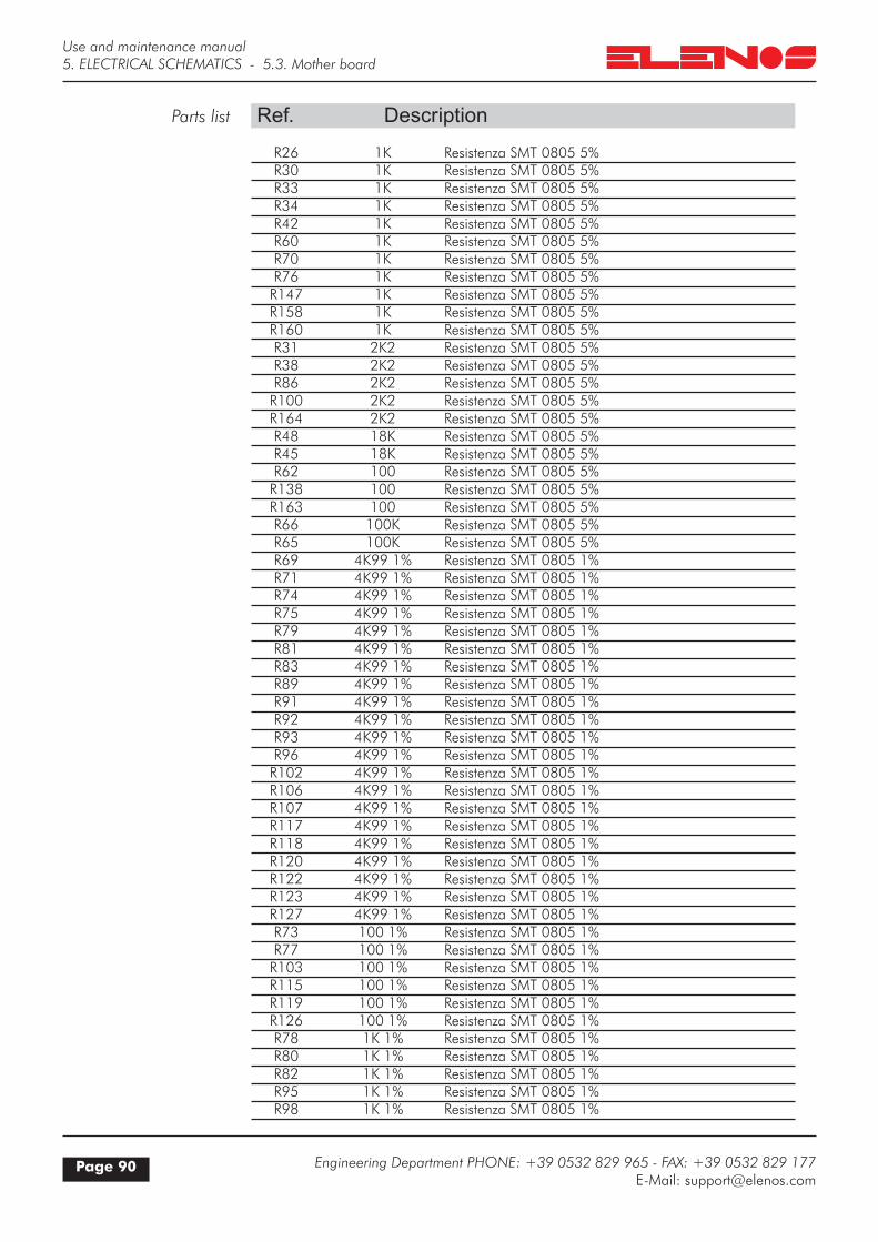
Use and maintenance manual
Page 90 Engineering Department PHONE: +39 0532 829 965 - FAX: +39 0532 829 177E-Mail: [email protected]
5. ELECTRICAL SCHEMATICS - 5.3. Mother board
Ref. DescriptionParts list
R26 1K Resistenza SMT 0805 5% R30 1K Resistenza SMT 0805 5% R33 1K Resistenza SMT 0805 5% R34 1K Resistenza SMT 0805 5% R42 1K Resistenza SMT 0805 5% R60 1K Resistenza SMT 0805 5% R70 1K Resistenza SMT 0805 5% R76 1K Resistenza SMT 0805 5% R147 1K Resistenza SMT 0805 5% R158 1K Resistenza SMT 0805 5% R160 1K Resistenza SMT 0805 5% R31 2K2 Resistenza SMT 0805 5% R38 2K2 Resistenza SMT 0805 5% R86 2K2 Resistenza SMT 0805 5% R100 2K2 Resistenza SMT 0805 5% R164 2K2 Resistenza SMT 0805 5% R48 18K Resistenza SMT 0805 5% R45 18K Resistenza SMT 0805 5% R62 100 Resistenza SMT 0805 5% R138 100 Resistenza SMT 0805 5% R163 100 Resistenza SMT 0805 5% R66 100K Resistenza SMT 0805 5% R65 100K Resistenza SMT 0805 5% R69 4K99 1% Resistenza SMT 0805 1% R71 4K99 1% Resistenza SMT 0805 1% R74 4K99 1% Resistenza SMT 0805 1% R75 4K99 1% Resistenza SMT 0805 1% R79 4K99 1% Resistenza SMT 0805 1% R81 4K99 1% Resistenza SMT 0805 1% R83 4K99 1% Resistenza SMT 0805 1% R89 4K99 1% Resistenza SMT 0805 1% R91 4K99 1% Resistenza SMT 0805 1% R92 4K99 1% Resistenza SMT 0805 1% R93 4K99 1% Resistenza SMT 0805 1% R96 4K99 1% Resistenza SMT 0805 1% R102 4K99 1% Resistenza SMT 0805 1% R106 4K99 1% Resistenza SMT 0805 1% R107 4K99 1% Resistenza SMT 0805 1% R117 4K99 1% Resistenza SMT 0805 1% R118 4K99 1% Resistenza SMT 0805 1% R120 4K99 1% Resistenza SMT 0805 1% R122 4K99 1% Resistenza SMT 0805 1% R123 4K99 1% Resistenza SMT 0805 1% R127 4K99 1% Resistenza SMT 0805 1% R73 100 1% Resistenza SMT 0805 1% R77 100 1% Resistenza SMT 0805 1% R103 100 1% Resistenza SMT 0805 1% R115 100 1% Resistenza SMT 0805 1% R119 100 1% Resistenza SMT 0805 1% R126 100 1% Resistenza SMT 0805 1% R78 1K 1% Resistenza SMT 0805 1% R80 1K 1% Resistenza SMT 0805 1% R82 1K 1% Resistenza SMT 0805 1% R95 1K 1% Resistenza SMT 0805 1% R98 1K 1% Resistenza SMT 0805 1%

Use and maintenance manual
Page 91Engineering Department PHONE: +39 0532 829 965 - FAX: +39 0532 829 177E-Mail: [email protected]
5. ELECTRICAL SCHEMATICS - 5.3. Mother board
Ref. DescriptionParts list
R99 1K 1% Resistenza SMT 0805 1% R112 1K 1% Resistenza SMT 0805 1% R85 47K Resistenza SMT 0805 5% R113 47K Resistenza SMT 0805 5% R149 47K Resistenza SMT 0805 5% R101 220 Resistenza SMT 0805 5% R87 220 Resistenza SMT 0805 5% R88 4K42 1% Resistenza SMT 0805 1% R90 47 Resistenza SMT 0805 5% R97 47 Resistenza SMT 0805 5% R128 47 Resistenza SMT 0805 5% R94 100R Resistenza SMT 0805 5% R111 100R Resistenza SMT 0805 5% R116 100R Resistenza SMT 0805 5% R114 6M8 Resistenza SMT 0805 5% R125 22K Resistenza SMT 0805 5% R130 2K7 Resistenza SMT 0805 5% R135 2K7 Resistenza SMT 0805 5% R151 2K7 Resistenza SMT 0805 5% R180 120 Resistenza SMT 0805 5% R132 120 Resistenza SMT 0805 5% R134 27 Resistenza SMT 0805 5% R139 56 Resistenza SMT 0805 5% R170 56 Resistenza SMT 0805 5% R176 56 Resistenza SMT 0805 5% R179 56 Resistenza SMT 0805 5% R184 56 Resistenza SMT 0805 5% R142 27K Resistenza SMT 0805 5% R165 27K Resistenza SMT 0805 5% R144 390 Resistenza SMT 0805 5% R145 1K5 Resistenza SMT 0805 5% R153 6K Resistenza SMT 0805 5% R154 12K Resistenza SMT 0805 5% R166 12K Resistenza SMT 0805 5% R167 12K Resistenza SMT 0805 5% R159 15K Resistenza SMT 0805 5% R178 270 Resistenza assiale 1/4W 10% R168 270 Resistenza assiale 1/4W 10% R169 620 Resistenza SMT 0805 5% R171 820 Resistenza SMT 0805 5% R173 330K Resistenza SMT 0805 5% R175 15 Resistenza SMT 0805 5% R181 20K Resistenza SMT 0805 5% SC1 SCREW Vite fissaggio N3X5mm SC2 SCREW Vite fissaggio N3X5mm SC3 SCREW Vite fissaggio N3X5mm SC4 SCREW Vite fissaggio N3X5mm SC5 SCREW Vite fissaggio N3X5mm SC6 SCREW Vite fissaggio N3X5mm SC7 SCREW Vite fissaggio N3X5mm SH1 VCO SHELD Scatolino VCO e PLL SH2 PLL SHELD Scatolino VCO e PLL TL1 75 ohm Cavo coassiale Belden TP1 INP Test point TP2 OUT Test point

Use and maintenance manual
Page 92 Engineering Department PHONE: +39 0532 829 965 - FAX: +39 0532 829 177E-Mail: [email protected]
5. ELECTRICAL SCHEMATICS - 5.3. Mother board
Ref. DescriptionParts list
TP3 SCA Test point TP4 LEV CC Test point TP5 Vpll TEST POINT Test point U2 LM324 IC SMT SOIC14 U1 LM324 IC SMT SOIC14 U3 LMC7101/SOT23 Op-Amp SMT SOT23-5 U8 LMC7101/SOT23 Op-Amp SMT SOT23-5 U14 LMC7101/SOT23 Op-Amp SMT SOT23-5 U21 LMC7101/SOT23 Op-Amp SMT SOT23-5 U4 PCF80C552 IC PLCC28 Con zoccolo U5 74HC138 IC SMT SOIC16 U6 74HC00 IC SMT SOIC14 U10 74HC574 IC SMT SOIC20 Wide U7 74HC574 IC SMT SOIC20 Wide U9 7421 IC SMT SOIC14 U11 TL7705 IC SMT SOIC8 U12 74HC08 U13 74HC157AS IC SMT SOIC16 U15 74HC573 IC SMT SOIC20 Wide U16 74HC245 IC SMT SOIC20 Wide U20 74HC245 IC SMT SOIC20 Wide U19 MAX485 IC SMT SOIC8 U17 MAX485 IC SMT SOIC8 U18 AT27C020/LCC IC PLCC32 Con zoccolo U22 62256 IC SMT SOIC28 Wide U23 ST24C02 IC SMT SOIC8 U24 MC74HC595 IC SMT SOIC16 U25 CS3310 IC SMT SOIC16 U27 MC33078 IC SMT SOIC8 U26 MC33078 IC SMT SOIC8 U28 SSM2404 IC SMT SOIC20 Wide U29 LF347 IC SMT SOIC14 U31 LF347 IC SMT SOIC14 U30 LF353 U32 LM79L05AC IC SMT SOIC8 U34 LF353 IC SMT SOIC8 U35 LM358 IC SMT SOIC8 U39 LM358 IC SMT SOIC8 U36 10MHz TCXO SMT MEC U37 H11F1 Fotoaccoppiatore Dip6 U38 LMX1501AM IC SMT SOIC16 U40 AD797 o NE5534 IC SMT SOIC8 U41 AD587 IC SMT SOIC8 (non montare) U42 ERA 3 MMIC U43 ERA 3 MMIC U44 74HC4067 IC SMT SOIC24 Wide VR1 100K Trimmer multigiri vert. oin in linea VR2 1K Trimmer multig. vert. pin in linea VR4 10K Trimmer multig. lungo orizz. VR3 10K Trimmer multig. lungo orizz. VR5 50K Trimmer multig. vert. pin in linea VR6 10K Trimmer multig. vert pin in linea Y1 16MHz Quarzo HC49

Use and maintenance manual
Page 93Engineering Department PHONE: +39 0532 829 965 - FAX: +39 0532 829 177E-Mail: [email protected]
5. ELECTRICAL SCHEMATICS - 5.4. Keyboard
ETG250/300
A.GiovannelliA.Tomassini
KEYB.ETG500V1.0A
Wednesday, November 15, 2000 11
KEYBOARD
1Model:
Approved :Proj. Engr. :
Website WWW.ELENOS.COM Tel +39 0532 829965 Fax +39 0532 829177 Via G.Amendola 9 44028 Poggio Renatico (FE) Italy
ofSheetDate:
RevBoard Code:
Title:

Use and maintenance manual
Page 94 Engineering Department PHONE: +39 0532 829 965 - FAX: +39 0532 829 177E-Mail: [email protected]
5. ELECTRICAL SCHEMATICS - 5.4. Keyboard

Pag 11 file A3Schema Keyboard


Use and maintenance manual
Page 97Engineering Department PHONE: +39 0532 829 965 - FAX: +39 0532 829 177E-Mail: [email protected]
5. ELECTRICAL SCHEMATICS - 5.4. Keyboard
Ref. DescriptionParts list
C3 10uF/25V C1 10uF/25V C2 100nF C4 100nF C8 100nF C5 10u C6 10u C7 10u D1 BAT64 H1 CON1 H2 CON1 H3 CON1 H4 CON1 H5 CON1 JD1 CON26 JP1 DISPLAY JP2 CONN 2 LD1 LED LD2 LED LD3 LED L1 2,2uH SW1 SWITCH P1 SWITCH P2 SWITCH P3 SWITCH P4 SWITCH P5 SWITCH P6 SWITCH P7 SWITCH P8 SWITCH Q1 BC817 Q2 BC817 Q3 BC817 RR1 10K R7 10K R9 10K R10 10K R12 10K R1 4K7 R2 N.M. R3 2K2 R4 1K VR1 1K R5 330 R8 330 R11 330 R6 VARISTOR R13 3,3 2W U1 14042 U2 74HC245 U3 LTC1054CN8

Use and maintenance manual
Page 98 Engineering Department PHONE: +39 0532 829 965 - FAX: +39 0532 829 177E-Mail: [email protected]
5. ELECTRICAL SCHEMATICS - 5.4. Keyboard

Use and maintenance manual
Page 99Engineering Department PHONE: +39 0532 829 965 - FAX: +39 0532 829 177E-Mail: [email protected]
5. ELECTRICAL SCHEMATICS - 5.5. Driver
E-ATG10-98-1.1
+
+
C8
C3
R13
C30
C23
C12 R5
L7L8
Q2
C5 R14
C16
C17
C19
L11
L6
L4
R8
C20
L10
C25
C24
R18
R6R15
R7
R2 R3
C13
C1
R12
R16L1
C26 C22C27 C21
L9
R19
L3C11
R4C15
C14
C6
R1
P1R10
R11
Q1
C2
C9
L2
R9
U1
ETG250/300
A.GiovannelliA.Tomassini
E-ATG-98-1.1
Wednesday, November 15, 2000 11
DRIVER
1.1Model:
Approved :Proj. Engr. :
Website WWW.ELENOS.COM Tel +39 0532 829965 Fax +39 0532 829177 Via G.Amendola 9 44028 Poggio Renatico (FE) Italy
ofSheetDate:
RevBoard Code:
Title:

Use and maintenance manual
Page 100 Engineering Department PHONE: +39 0532 829 965 - FAX: +39 0532 829 177E-Mail: [email protected]
5. ELECTRICAL SCHEMATICS - 5.5. Driver
+VCC
VCC +12V
2.7
R9
2u2L9
4n7
C6
5sp1mmD6L8L3
ERA 5
U1
75pFC11
INGRESSO max. +7dBm
J1
560R5
10nC8
39pFC12
100R10
10R12
2u2L2
18R3
4n7C3
+10uFC26
560R4
33KR1
1000R19
300pFC23
47nC21
75pFC19
+
10uFC27
680R8
10nC20
3sp1mmD6L8
L11
47KR7
47R15
USCITA
J2
12R18
1nC5
VK200L10
120pFC173sp1mmD6L9
L8
43pFC15 BLF244
Q2
4.7nC25
5sp1mmD8L5L4
6K8R6
3sp1mmD6L6
L6
2.2R14
10nC14
300pFC16
4.7nC24
1nC1
BLF404Q1
18R2
10nC9
4n7C2
4sp1mmD6L6L7
VK200
L1
10KR18 12K
R11
47R16
10nC13
4n7
C30
47R13
47nC22
ETG250/300
A.GiovannelliA.Tomassini
E-ATG10-98-1.1
Wednesday, November 15, 2000 11
DRIVER
1.1Model:
Approved :Proj. Engr. :
Website WWW.ELENOS.COM Tel +39 0532 829965 Fax +39 0532 829177 Via G.Amendola 9 44028 Poggio Renatico (FE) Italy
ofSheetDate:
RevBoard Code:
Title:
41
18V< +VCC <28V

Use and maintenance manual
Page 101Engineering Department PHONE: +39 0532 829 965 - FAX: +39 0532 829 177E-Mail: [email protected]
5. ELECTRICAL SCHEMATICS - 5.5. Driver
Ref. DescriptionParts list
C1 1n C5 1n C2 4n7 C3 4n7 C6 4n7 C30 4n7 C8 10n C9 10n C13 10n C14 10n C20 10n C19 75pF C11 75pF C12 39pF C15 43pF C16 300pF C23 300pF C17 120pF C22 47n C21 47n C24 4.7n C25 4.7n C27 10uF C26 10uF J1 INGRESSO max. +7dBm J2 USCITA L1 VK200 L10 VK200 L2 2u2 L9 2u2 L3 5sp1mmD6L8 L4 5sp1mmD8L5 L6 3sp1mmD6L6 L7 4sp1mmD6L6 L8 3sp1mmD6L9 L11 3sp1mmD6L8 Q1 BLF404 Q2 BLF244 R1 33K R2 18 R3 18 R4 560 R5 560 R6 6K8 R7 47K R8 680 R9 2.7 R10 100 R11 12K R12 10 R13 47 R15 47 R16 47 R14 2.2 R18 10K

Use and maintenance manual
Page 102 Engineering Department PHONE: +39 0532 829 965 - FAX: +39 0532 829 177E-Mail: [email protected]
5. ELECTRICAL SCHEMATICS - 5.5. Driver
Ref. DescriptionParts list
R18 12 R19 1000 U1 ERA 5

Use and maintenance manual
Page 103Engineering Department PHONE: +39 0532 829 965 - FAX: +39 0532 829 177E-Mail: [email protected]
5. ELECTRICAL SCHEMATICS - 5.6. RF final output stage
ETG250/300
A.GiovannelliA.Tomassini
E-ATG300-1.1
Wednesday, November 15, 2000 11
POWER AMPLIFIER
1.1Model:
Approved :Proj. Engr. :
Website WWW.ELENOS.COM Tel +39 0532 829965 Fax +39 0532 829177 Via G.Amendola 9 44028 Poggio Renatico (FE) Italy
ofSheetDate:
RevBoard Code:
Title:
2PC
B02
52_1
C1
2PC
B02
52_1
C1
TF1 TF1
R7 R7R2
U1 U1
P1 P1C5 C5
C6 C6
C4 C4
D1 D1
C9C10
C9C10
C2 C2
C3R1
C3R1
+VDS +VDS
L2 L2
R9 R9C13 C13
C12 C12C11 C11C15 C15
C14 C14
C18C19
C18C19C16
C17C16
C17
GATE BIASVOLTAGE
GATE BIASVOLTAGE
L1 L1
R8 R8
25 Ohm 25 Ohm25 Ohm
50 Ohm 50 Ohm
25 Ohm
C7C8
C7C8
R6 R6
R3R2R3
R4R5
R4R5
++

Use and maintenance manual
Page 104 Engineering Department PHONE: +39 0532 829 965 - FAX: +39 0532 829 177E-Mail: [email protected]
5. ELECTRICAL SCHEMATICS - 5.6. RF final output stage
ETG250/300
A.GiovannelliA.Tomassini
E-AT300-1.1
Wednesday, November 15, 2000 11
POWER AMPLIFIER
1.1Model:
Approved :Proj. Engr. :
Website WWW.ELENOS.COM Tel +39 0532 829965 Fax +39 0532 829177 Via G.Amendola 9 44028 Poggio Renatico (FE) Italy
ofSheetDate:
RevBoard Code:
Title:
R7
22
C17
470p
F
C7
10nF
C8
10nF
C6
10nF
C10
10nF
C9
10nF
D11N4148
R3
10
R4
10R
510C
410
nF
C5
10nF
C1
56pF
J1
L3 70uH
C3
10nF
25 o
hms
25 o
hms
50 o
hms
C2
10nF
R8
10
J2
U1
BLF
278
TF
1
C14
470p
F
R6
10K
P120K R1
10K R
2 10
C12
470p
F
C13
47uF
63V
+
C15
470p
F
C11
470p
F
C18
470p
F
C19
470p
F
L1
C16
470p
F
R9 10
L2 430n
H
+VD
S
GA
TE
BIA
S V
OLT
AG
E

Use and maintenance manual
Page 105Engineering Department PHONE: +39 0532 829 965 - FAX: +39 0532 829 177E-Mail: [email protected]
5. ELECTRICAL SCHEMATICS - 5.6. RF final output stage
Ref. DescriptionParts list
C1 56pF C2 10nF C3 10nFC4 10nFC5 10nFC6 10nFC7 10nFC8 10nFC9 10nFC10 10nFC14 470pF C11 470pF C12 470pFC15 470pFC16 470pFC17 470pFC18 470pFC19 470pFC13 47uF 63VD1 1N4148J1 SMA CS VERTJ2 BNCL1 INDL2 430nHL3 70uHP1 20KR6 10KR1 10KR2 10R3 10R4 10R5 10R8 10R9 10R7 22TF1 TF2 25 ohmsTF3 25 ohmsTF4 50 ohmsU1 BLF278

Use and maintenance manual
Page 106 Engineering Department PHONE: +39 0532 829 965 - FAX: +39 0532 829 177E-Mail: [email protected]
5. ELECTRICAL SCHEMATICS - 5.6. RF final output stage

Use and maintenance manual
Page 107Engineering Department PHONE: +39 0532 829 965 - FAX: +39 0532 829 177E-Mail: [email protected]
5. ELECTRICAL SCHEMATICS - 5.7. LP filter
ETG250-300
A.GiovannelliA.Tomassini
2PCB0266B
Wednesday, November 15, 2000 11
LPF AND POWER PROBE
1Model:
Approved :Proj. Engr. :
Website WWW.ELENOS.COM Tel +39 0532 829965 Fax +39 0532 829177 Via G.Amendola 9 44028 Poggio Renatico (FE) Italy
ofSheetDate:
RevBoard Code:
Title:

Use and maintenance manual
Page 108 Engineering Department PHONE: +39 0532 829 965 - FAX: +39 0532 829 177E-Mail: [email protected]
5. ELECTRICAL SCHEMATICS - 5.7. LP filter
ETG250-300
A.GiovannelliA.Tomassini
2PCB0266B
Wednesday, November 15, 2000 31
POWER PROBES
1Model:
Approved :Proj. Engr. :
Website WWW.ELENOS.COM Tel +39 0532 829965 Fax +39 0532 829177 Via G.Amendola 9 44028 Poggio Renatico (FE) Italy
ofSheetDate:
RevBoard Code:
Title:
RF out
13
2
13
2
C8
33pF
R4500
R5C100
D2hsms2850
D1
HSMS 2850
R6330
R5330
R7500 ohm
C9
33pF
R1
12K
R2
12K
C7
4.7nF
C6
4.7nF
CL1220pF
R3 500
input1 input2
testina
RF SAMPLE

Use and maintenance manual
Page 109Engineering Department PHONE: +39 0532 829 965 - FAX: +39 0532 829 177E-Mail: [email protected]
5. ELECTRICAL SCHEMATICS - 5.7. LP filter
ETG250-300
A.GiovannelliA.Tomassini
2PCB0266B
Wednesday, November 15, 2000 32
POWER PROBE AMPLIFIER
1Model:
Approved :Proj. Engr. :
Website WWW.ELENOS.COM Tel +39 0532 829965 Fax +39 0532 829177 Via G.Amendola 9 44028 Poggio Renatico (FE) Italy
ofSheetDate:
RevBoard Code:
Title:
12v
5
3
1
2
4
13
2
1 3
2
1234
5
3
1
2
4
R3B
1
27K
R92K
2
R14
100
NT
C1
100K
R11
27K
C17
100nF
C18
100nF
R12
220K
R13
220k
R10
47
AR
1
LMC
7101
V-
V+
+-
PR
2500
C13
100nF
C14
100nF
PR
1500
JP1
2PJ00134
R15100
C15
4.7nF
R16
47
C16
4.7nF
R1B
1
2K2
AR
2
LMC
7101V
-
V+
+-
NT
CB
1
100K
12v
input1input2
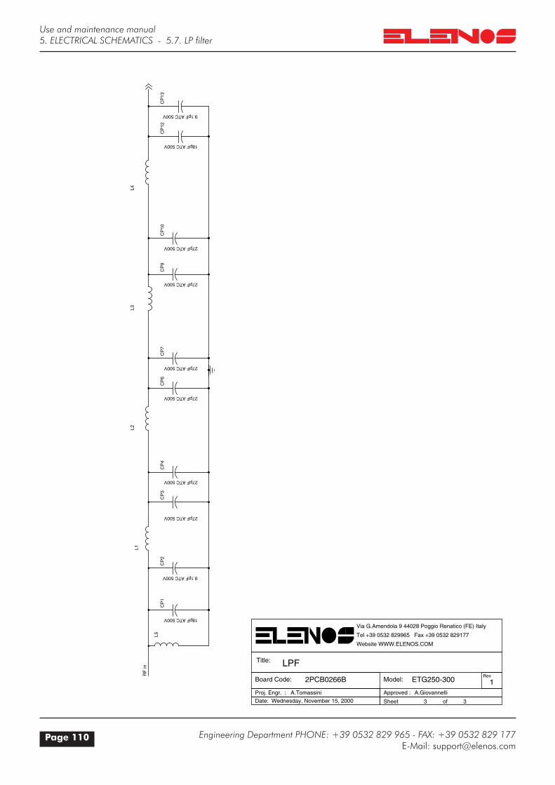
Use and maintenance manual
Page 110 Engineering Department PHONE: +39 0532 829 965 - FAX: +39 0532 829 177E-Mail: [email protected]
5. ELECTRICAL SCHEMATICS - 5.7. LP filter
ETG250-300
A.GiovannelliA.Tomassini
2PCB0266B
Wednesday, November 15, 2000 33
LPF
1Model:
Approved :Proj. Engr. :
Website WWW.ELENOS.COM Tel +39 0532 829965 Fax +39 0532 829177 Via G.Amendola 9 44028 Poggio Renatico (FE) Italy
ofSheetDate:
RevBoard Code:
Title:
RF
in
L5
L1L3
L4L2
CP
2
9.1pF ATC 500V
CP
13
9.1pF ATC 500V
CP
7
27pF ATC 500V
CP
118pF ATC 500V
CP
3
27pF ATC 500V
CP
10
27pF ATC 500V
CP
6
27pF ATC 500V
CP
9
27pF ATC 500V
CP
12
18pF ATC 500V
CP
4
27pF ATC 500V

Use and maintenance manual
Page 111Engineering Department PHONE: +39 0532 829 965 - FAX: +39 0532 829 177E-Mail: [email protected]
5. ELECTRICAL SCHEMATICS - 5.7. LP filter
Ref. DescriptionParts list
AR1 LMC7101 AR2 LMC7101 CL1 220pF CP1 18pF ATC 500V CP12 18pF ATC 500V CP2 9.1pF ATC 500V CP13 9.1pF ATC 500V CP3 27pF ATC 500V CP4 27pF ATC 500V CP6 27pF ATC 500V CP7 27pF ATC 500V CP9 27pF ATC 500V CP10 27pF ATC 500V C6 4.7nF C7 4.7nF C15 4.7nF C8 33pF C9 33pF C13 100nF C14 100nF C16 4.7nF C17 100nF C18 100nF D1 HSMS 2850 D2 hsms2850 JP1 2PJ00134 L1 vedi note L2 vedi note L3 vedi note L4 vedi note L5 vedi note NTC1 100K NTCB1 100K PR1 500 PR2 500 R3 500 R4 500 R1 12K R2 12K R5C 100 R6 330 R5 330 R7 500 ohm R9 2K2 R1B1 2K2 R10 47 R16 47 R11 27K R12 220K R13 220k R14 100 R15 100 R3B1 27K

Use and maintenance manual
Page 112 Engineering Department PHONE: +39 0532 829 965 - FAX: +39 0532 829 177E-Mail: [email protected]
5. ELECTRICAL SCHEMATICS - 5.7. LP filter

Use and maintenance manual
Page 113Engineering Department PHONE: +39 0532 829 965 - FAX: +39 0532 829 177E-Mail: [email protected]
5. ELECTRICAL SCHEMATICS - 5.8. Input output combiner system
Driv
erLP
FO
UT
50Ω
RG
303
50Ω
RG
178
PO
WE
R
AM
PLI
FIE
R
ETG250/300
A.GiovannelliA.Tomassini
Wednesday, November 15, 2000 11
SPLITTER INPUT AND COMBINER OUTPUT
1Model:
Approved :Proj. Engr. :
Website WWW.ELENOS.COM Tel +39 0532 829965 Fax +39 0532 829177 Via G.Amendola 9 44028 Poggio Renatico (FE) Italy
ofSheetDate:
RevBoard Code:
Title:

Use and maintenance manual
Page 114 Engineering Department PHONE: +39 0532 829 965 - FAX: +39 0532 829 177E-Mail: [email protected]
5. ELECTRICAL SCHEMATICS - 5.8. Input output combiner system

Use and maintenance manual
Page 115Engineering Department PHONE: +39 0532 829 965 - FAX: +39 0532 829 177E-Mail: [email protected]
5. ELECTRICAL SCHEMATICS - 5.9. BUS board
ETG250/300
A.GiovannelliA.Tomassini
ETG500BU
Wednesday, November 15, 2000 11
BUS
1.1Model:
Approved :Proj. Engr. :
Website WWW.ELENOS.COM Tel +39 0532 829965 Fax +39 0532 829177 Via G.Amendola 9 44028 Poggio Renatico (FE) Italy
ofSheetDate:
RevBoard Code:
Title:
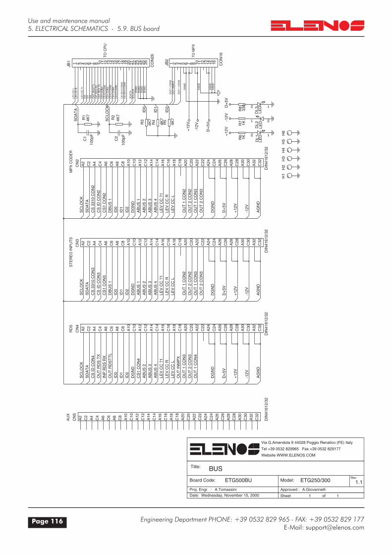
Use and maintenance manual
Page 116 Engineering Department PHONE: +39 0532 829 965 - FAX: +39 0532 829 177E-Mail: [email protected]
5. ELECTRICAL SCHEMATICS - 5.9. BUS board
+12
V
-12V
D+
5V
D+
5V
-12V
+12
V
100p
F
C1
4K7
R1
H3
H2
DIN
4161
2/32
CN
5
LED
DL1
LED
DL2
LED
DL3
4K7
R2
100p
F
C2
4K7
R5
4K7
R4
4K7
R3
DIN
4161
2/32
CN
3
H6
H1
CO
N16
JB2
330
R8
CO
N26
JB1
1KR7
DIN
4161
2/32
CN
4
H4
1KR6
DIN
4161
2/32
CN
2
H5
1
1
C32
C30
C28
C26
C24
C22
C20
C18
C16
C14
C12
C10
C8
C6
C4
C2
A32
A30
A28
A26
A24
A22
A20
A18
A16
A14
A12
A10
A8
A6
A4
A2
12
1 2
12
C32
C30
C28
C26
C24
C22
C20
C18
C16
C14
C12
C10
C8
C6
C4
C2
A32
A30
A28
A26
A24
A22
A20
A18
A16
A14
A12
A10
A8
A6
A4
A2
1
1
161514131211109876543212625242322212019181716151413121110987654321
C32
C30
C28
C26
C24
C22
C20
C18
C16
C14
C12
C10
C8
C6
C4
C2
A32
A30
A28
A26
A24
A22
A20
A18
A16
A14
A12
A10
A8
A6
A4
A2
1
C32
C30
C28
C26
C24
C22
C20
C18
C16
C14
C12
C10
C8
C6
C4
C2
A32
A30
A28
A26
A24
A22
A20
A18
A16
A14
A12
A10
A8
A6
A4
A2
1
AG
ND
AG
ND
DG
ND
-12V
AG
ND
DG
ND
AG
ND
D+
5V
DG
ND
-12V
AG
ND
+12
V
D+
5V
DG
ND
-12V
DG
ND
DG
ND
DG
ND
D+
5V
DG
ND
DG
ND
AG
ND
DG
ND
+12
V+
12V
DG
ND
SC
LOC
K
SD
AT
A
OU
T 1
CO
N2
OU
T IN
MP
X
OU
T 1
CO
N4
OU
T IN
MP
X
ID0
OU
T R
DS
TT
L
LEV
CC
?1
ID2
LEV
CC
RLE
V C
C L
CS
1 C
ON
2
CS
331
0 C
ON
3C
S 3
310
CO
N2
SD
AT
A
CS
ID C
ON
4
SC
LOC
K
OU
T R
DS
TX
CS
1 C
ON
3
ID1
CS
ID C
ON
3
CS
ID C
ON
2
CS
1 C
ON
4
INP
RD
S R
X
OU
T 2
CO
N3
OU
T 2
CO
N3
OU
T 1
CO
N3
OU
T 1
CO
N3
OU
T 1
CO
N4
OU
T 2
CO
N2
OU
T 2
CO
N2
OU
T 2
CO
N3
ID2
OU
T 1
CO
N2
OU
T 1
CO
N2
OU
T 1
CO
N3
ID1
LEV
CC
LLE
V C
C L
LEV
CC
LLE
V C
C R
LEV
CC
RLE
V C
C R
ID0
LEV
CC
?1
LEV
CC
?1
LEV
CC
?1
AB
US
4A
BU
S 4
AB
US
4A
BU
S 3
AB
US
3A
BU
S 3
AB
US
2A
BU
S 2
AB
US
2A
BU
S 1
AB
US
1C
S1
CO
N4
ID2
ID2
ID2
ID1
ID1
ID1
ID0
ID0
ID0
DB
US
1D
BU
S 1
OU
T R
DS
TT
LC
S1
CO
N2
CS
1 C
ON
3IN
P R
DS
RX
CS
ID C
ON
2C
S ID
CO
N3
OU
T R
DS
TX
CS
331
0 C
ON
2C
S 3
310
CO
N3
CS
ID C
ON
4S
DA
TA
SD
AT
AS
DA
TA
SC
LOC
KS
CLO
CK
SC
LOC
K
TO
MP
X
TO
CP
U
RD
SS
TE
RE
O IN
PU
TS
MP
X C
OD
ER
AU
X
ETG250/300
A.GiovannelliA.Tomassini
ETG500BU
Wednesday, November 15, 2000 11
BUS
1.1Model:
Approved :Proj. Engr. :
Website WWW.ELENOS.COM Tel +39 0532 829965 Fax +39 0532 829177 Via G.Amendola 9 44028 Poggio Renatico (FE) Italy
ofSheetDate:
RevBoard Code:
Title:
Use and maintenance manual
Page 117Engineering Department PHONE: +39 0532 829 965 - FAX: +39 0532 829 177E-Mail: [email protected]
5. ELECTRICAL SCHEMATICS - 5.9. BUS board
Ref. DescriptionParts list
CN2 DIN41612/32CN3 DIN41612/32CN4 DIN41612/32CN5 DIN41612/32C2 100pFC1 100pFDL1 LEDDL2 LEDDL3 LEDH1 CON1H2 CON1H3 CON1H4 CON1H5 CON1H6 CON1JB1 CON26JB2 CON16R1 4K7R2 4K7R3 4K7R4 4K7R5 4K7R6 1KR7 1KR8 330

Use and maintenance manual
Page 118 Engineering Department PHONE: +39 0532 829 965 - FAX: +39 0532 829 177E-Mail: [email protected]
5. ELECTRICAL SCHEMATICS - 5.9. BUS board
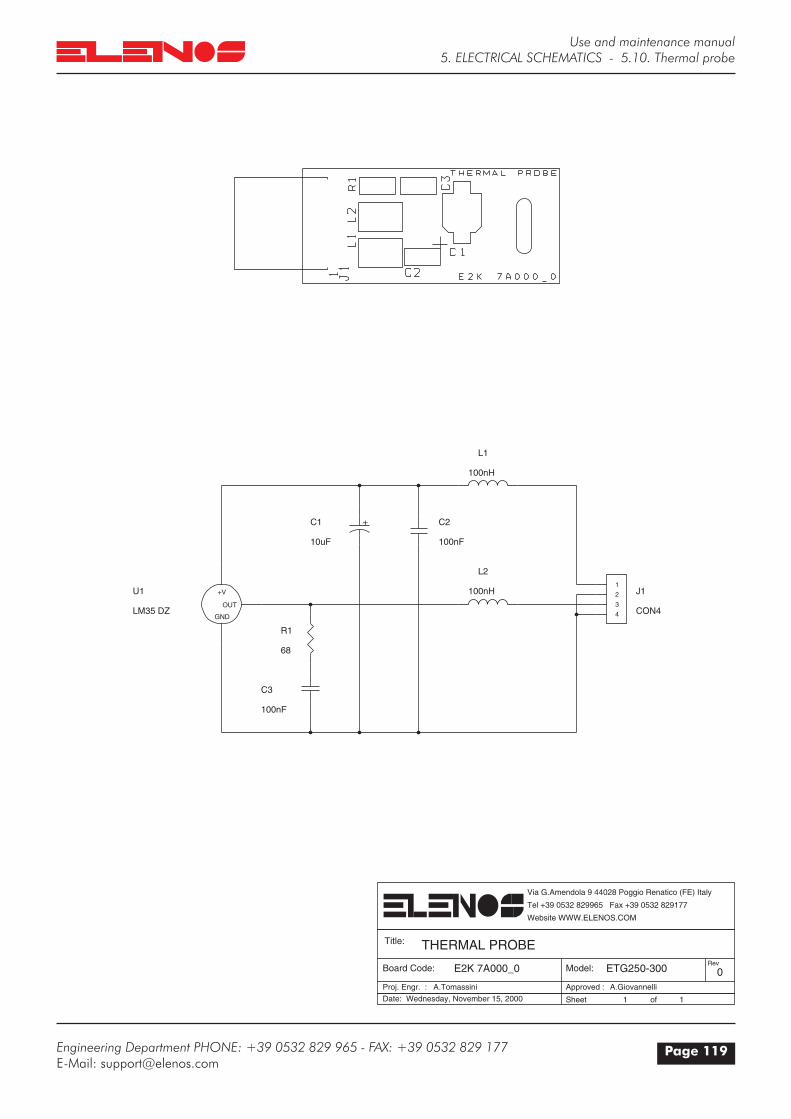
Use and maintenance manual
Page 119Engineering Department PHONE: +39 0532 829 965 - FAX: +39 0532 829 177E-Mail: [email protected]
5. ELECTRICAL SCHEMATICS - 5.10. Thermal probe
ETG250-300
A.GiovannelliA.Tomassini
E2K 7A000_0
Wednesday, November 15, 2000 11
THERMAL PROBE
0Model:
Approved :Proj. Engr. :
Website WWW.ELENOS.COM Tel +39 0532 829965 Fax +39 0532 829177 Via G.Amendola 9 44028 Poggio Renatico (FE) Italy
ofSheetDate:
RevBoard Code:
Title:
100nH
L1
100nH
L2
+
10uF
C1
CON4
J1
100nF
C2
OUT
GND
+V
LM35 DZ
U1
100nF
C3
68
R1
4
3
2
1

Use and maintenance manual
Page 120 Engineering Department PHONE: +39 0532 829 965 - FAX: +39 0532 829 177E-Mail: [email protected]
5. ELECTRICAL SCHEMATICS - 5.10. Thermal probe
Ref. DescriptionParts list
C1 10uF C3 100nF C2 100nF J1 CON4 L2 100nH L1 100nH R1 68 U1 LM35 DZ

Use and maintenance manual
Page 121Engineering Department PHONE: +39 0532 829 965 - FAX: +39 0532 829 177E-Mail: [email protected]
6. TROUBLESHOOTING
TROUBLESHOOTING GUIDE
Problem
The unit will not power up
The unit does not reach required power level
The unit transmits on the wrong frequency
Absence of modulation on the output and on the display
Absence of modulation on the output but not on the display
Modulation does not reach the required value
Absence of stereo modulation
Absence of RDS transmission
Solution
Connect or replace power cable and try again
Replace the fuses and try again
Contact the manufacturer
Access the RF menu and enable “RF On”
Connect the antenna or amplifier (check the integrity of the connection)
Contact the manufacturer
Contact the manufacturer
Contact the manufacturer
Connect or replace the audio cable
Contact the manufacturer Enable modulation from the audio
menu
Contact the manufacturer
Increase the audio input level
Contact the manufacturer
Set the correct threshold
Enable stereo carrier from the user setup menu
Connect or replace the audio cable
Contact the manufacturer Insert stereo board and/or stereo
encoder
Switch on RDS from the user setup menu
Reprogram RDS board Insert RDS board
Cause
Power cable missing or faulty
Power supply fuses (rear panel ) blown
Auxiliary power supply faulty (“MAIN” front panel led not lit)
Unit in Stand-By
Antenna or amplifier not connected
PLL unlocked (“ON Air” front panel indicator not lit)
Power supply or RF module faulty
PLL board faulty
Missing or faulty audio cable
MPX board faulty Modulation switched off
MPX board faulty
Low audio input level
MPX board faulty
ALC threshold programming error
Stereo carrier disabled
Missing or damaged audio cable
Stereo board faulty Missing stereo board and/or stereo
encoder
RDS switched off
RDS message programming error RDS board missing

Use and maintenance manual
Page 122 Engineering Department PHONE: +39 0532 829 965 - FAX: +39 0532 829 177E-Mail: [email protected]
6. TROUBLESHOOTING
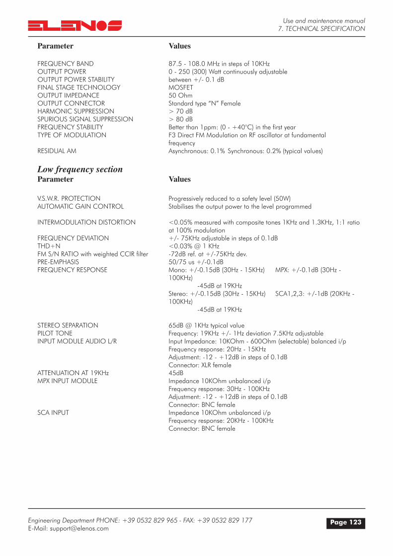
Use and maintenance manual
Page 123Engineering Department PHONE: +39 0532 829 965 - FAX: +39 0532 829 177E-Mail: [email protected]
7. TECHNICAL SPECIFICATION
Parameter Values
FREQUENCY BAND 87.5 - 108.0 MHz in steps of 10KHzOUTPUT POWER 0 - 250 (300) Watt continuously adjustableOUTPUT POWER STABILITY between +/- 0.1 dBFINAL STAGE TECHNOLOGY MOSFETOUTPUT IMPEDANCE 50 OhmOUTPUT CONNECTOR Standard type “N” FemaleHARMONIC SUPPRESSION > 70 dBSPURIOUS SIGNAL SUPPRESSION > 80 dBFREQUENCY STABILITY Better than 1ppm: (0 - +40°C) in the first yearTYPE OF MODULATION F3 Direct FM Modulation on RF oscillator at fundamental frequencyRESIDUAL AM Asynchronous: 0.1% Synchronous: 0.2% (typical values)
Low frequency sectionParameter Values
V.S.W.R. PROTECTION Progressively reduced to a safety level (50W)AUTOMATIC GAIN CONTROL Stabilises the output power to the level programmed INTERMODULATION DISTORTION <0.05% measured with composite tones 1KHz and 1.3KHz, 1:1 ratio at 100% modulationFREQUENCY DEVIATION +/- 75KHz adjustable in steps of 0.1dBTHD+N <0.03% @ 1 KHzFM S/N RATIO with weighted CCIR filter -72dB ref. at +/-75KHz dev.PRE-EMPHASIS 50/75 us +/-0.1dBFREQUENCY RESPONSE Mono: +/-0.15dB (30Hz - 15KHz) MPX: +/-0.1dB (30Hz - 100KHz) -45dB at 19KHz Stereo: +/-0.15dB (30Hz - 15KHz) SCA1,2,3: +/-1dB (20KHz - 100KHz) -45dB at 19KHz
STEREO SEPARATION 65dB @ 1KHz typical valuePILOT TONE Frequency: 19KHz +/- 1Hz deviation 7.5KHz adjustableINPUT MODULE AUDIO L/R Input Impedance: 10KOhm - 600Ohm (selectable) balanced i/p Frequency response: 20Hz - 15KHz Adjustment: -12 - +12dB in steps of 0.1dB Connector: XLR femaleATTENUATION AT 19KHz 45dBMPX INPUT MODULE Impedance 10KOhm unbalanced i/p Frequency response: 30Hz - 100KHz Adjustment: -12 - +12dB in steps of 0.1dB Connector: BNC femaleSCA INPUT Impedance 10KOhm unbalanced i/p Frequency response: 20KHz - 100KHz Connector: BNC female

Use and maintenance manual
Page 124 Engineering Department PHONE: +39 0532 829 965 - FAX: +39 0532 829 177E-Mail: [email protected]
7. TECHNICAL SPECIFICATION
BROADCAST EQUIPMENT COMPANY
General characteristicsParameter Value
AMBIENT CONDITIONS Temperature: Humidity (operating): 0- +45°C (operating): 95% at 40°C (non operating): -20 - +50°C (non operating): 90% at 65°C Altitude: (operating): >4600 metres (non operating): >15000 metres
Parameter Value
WEIGHT 20Kg switch-mode version 30Kg transformer versionDIMENSIONS 50x14x50 cmPOWER SUPPLY 110-240VPOWER CONSUMPTION 400W typical at maximum power output ETG250 500W typical at maximum power output ETG300COOLING Forced ventilation
Limitations on cable lengths
RS232 connection cable less than 1m.MPX connection cable less than 1m.SCA1 connection cable less than 1m.SCA2 connection cable less than 1m.Power supply cable length less than 3 m.
Via G. Amendola 9 - 44028 Poggio Renatico (FE) - ItalyTel. +39 0532 829 965 - Fax +39 0532 829 177
E-Mail: [email protected] address: www.elenos.com