Embed Size (px)
Citation preview

Data sheet
BMC050 Electronic Compass
BMC050: Data sheet
Document revision 1.0
Document release date October 28th, 2011
Document number BST-BMC050-DS000-10
Technical reference code(s) 0 273 141 124
Notes Data in this document are preliminary and subject to change without notice. Product photos and pictures are for illustration purposes only and may differ from the real product‟s appearance. This document is confidential and under NDA.
Bosch Sensortec

Datasheet
BMC050 Electronic Compass Page 2
Confidential
BST-BMC050-DS000-10 | Revision 1.0 | October 2011 Bosch Sensortec
© Bosch Sensortec GmbH reserves all rights even in the event of industrial property rights. We reserve all rights of disposal such as copying and passing on to
third parties. BOSCH and the symbol are registered trademarks of Robert Bosch GmbH, Germany.
Note: Specifications within this document are subject to change without notice. Not intended for publication.
BMC050
ELECTRONIC COMPASS WITH THREE-AXIS MAGNETIC FIELD SENSOR
AND THREE-AXIS ACCELEROMETER
Key features
Three-axis magnetic field sensor and three-axis accelerometer in one package
Accelerometer can still be used independently from magnetometer operation
Ultra-Small package LGA package (16 pins), footprint 3mm x 3mm, height 0.95mm
Digital interface SPI (4-wire, 3-wire), I²C, 4 interrupt pins (2 acceleration sensor, 2 magnetic sensor interrupt pins)
Low voltage operation VDD supply voltage range: 1.62V to 3.6V VDDIO interface voltage range: 1.2V to 3.6V
Flexible functionality Acceleration ranges ±2g / ±4g / ±8g / ±16g Acceleration Low-pass filter bandwidths 1 kHz - <8Hz Magnetic field range typical ±1000µT Magnetic field resolution of ~0.3µT
On-chip interrupt controller Motion-triggered interrupt-signal generation for - new data (separate for accelerometer and magnetometer) - any-motion (slope) detection - tap sensing (single tap / double tap) - orientation recognition - flat detection - low-g/high-g detection - magnetic Low-/High-Threshold detection
Ultra-low power Low current consumption (190µA @ 10 Hz including accelerometer and magnetic sensor in low power preset), short wake-up time, advanced features for system power management
Temperature range -40 °C … +85 °C
RoHS compliant, halogen-free
Typical applications
Tilt-compensated electronic compass for map rotation, navigation and augmented reality
6-axis orientation for gaming
Display profile switching
Menu scrolling, tap / double tap sensing
Pedometer / step counting
Free-fall detection
Drop detection for warranty logging
Advanced system power management for mobile applications
Datasheet
BMC050 Electronic Compass Page 3
Confidential
BST-BMC050-DS000-10 | Revision 1.0 | October 2011 Bosch Sensortec
© Bosch Sensortec GmbH reserves all rights even in the event of industrial property rights. We reserve all rights of disposal such as copying and passing on to
third parties. BOSCH and the symbol are registered trademarks of Robert Bosch GmbH, Germany.
Note: Specifications within this document are subject to change without notice. Not intended for publication.
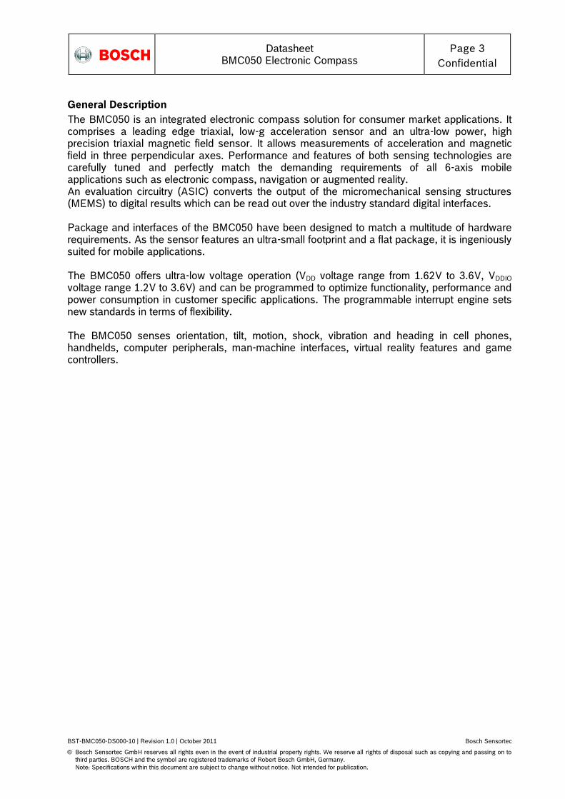
General Description
The BMC050 is an integrated electronic compass solution for consumer market applications. It comprises a leading edge triaxial, low-g acceleration sensor and an ultra-low power, high precision triaxial magnetic field sensor. It allows measurements of acceleration and magnetic field in three perpendicular axes. Performance and features of both sensing technologies are carefully tuned and perfectly match the demanding requirements of all 6-axis mobile applications such as electronic compass, navigation or augmented reality. An evaluation circuitry (ASIC) converts the output of the micromechanical sensing structures (MEMS) to digital results which can be read out over the industry standard digital interfaces. Package and interfaces of the BMC050 have been designed to match a multitude of hardware requirements. As the sensor features an ultra-small footprint and a flat package, it is ingeniously suited for mobile applications. The BMC050 offers ultra-low voltage operation (VDD voltage range from 1.62V to 3.6V, VDDIO
voltage range 1.2V to 3.6V) and can be programmed to optimize functionality, performance and power consumption in customer specific applications. The programmable interrupt engine sets new standards in terms of flexibility. The BMC050 senses orientation, tilt, motion, shock, vibration and heading in cell phones, handhelds, computer peripherals, man-machine interfaces, virtual reality features and game controllers.

Datasheet
BMC050 Electronic Compass Page 4
Confidential
BST-BMC050-DS000-10 | Revision 1.0 | October 2011 Bosch Sensortec
© Bosch Sensortec GmbH reserves all rights even in the event of industrial property rights. We reserve all rights of disposal such as copying and passing on to
third parties. BOSCH and the symbol are registered trademarks of Robert Bosch GmbH, Germany.
Note: Specifications within this document are subject to change without notice. Not intended for publication.
Index of Contents
1. SPECIFICATION ........................................................................................................................ 7
1.1 COMPASS ELECTRICAL SPECIFICATION ................................................................................. 7
1.2 ACCELEROMETER SPECIFICATION ........................................................................................ 7
1.3 MAGNETOMETER SPECIFICATION ......................................................................................... 9
2. ABSOLUTE MAXIMUM RATINGS .......................................................................................... 12
3. BLOCK DIAGRAM ................................................................................................................... 13
4. FUNCTIONAL DESCRIPTION ................................................................................................. 14
4.1 POWER MANAGEMENT ....................................................................................................... 14
4.2 PROTOCOL SELECTION ...................................................................................................... 14
4.3 POWER MODES ................................................................................................................. 15
4.3.1 ACCELEROMETER POWER MODES ................................................................................................. 15 4.3.2 MAGNETOMETER POWER MODES .................................................................................................. 18 4.3.3 BMC050 OVERALL POWER CONSUMPTION .................................................................................... 21
4.4 SENSOR DATA .................................................................................................................. 21
4.4.1 ACCELERATION DATA ................................................................................................................... 21 4.4.2 TEMPERATURE DATA .................................................................................................................... 23 4.4.3 MAGNETIC FIELD DATA .................................................................................................................. 23 4.4.4 MAGNETIC FIELD DATA TEMPERATURE COMPENSATION................................................................... 25
4.5 SELF-TEST ....................................................................................................................... 26
4.5.1 ACCELEROMETER SELF-TEST ........................................................................................................ 26 4.5.2 MAGNETOMETER SELF-TEST ......................................................................................................... 26
4.6 ACCELEROMETER OFFSET COMPENSATION ......................................................................... 28
4.6.1 SLOW COMPENSATION .................................................................................................................. 29 4.6.2 FAST COMPENSATION ................................................................................................................... 30 4.6.3 MANUAL COMPENSATION .............................................................................................................. 31 4.6.4 INLINE CALIBRATION ..................................................................................................................... 31
4.7 NON-VOLATILE MEMORY .................................................................................................... 32
4.7.1 ACCELEROMETER NON-VOLATILE MEMORY .................................................................................... 32 4.7.2 MAGNETOMETER NON-VOLATILE MEMORY ..................................................................................... 32
4.8 ACCELEROMETER INTERRUPT CONTROLLER ....................................................................... 33
4.8.1 GENERAL FEATURES .................................................................................................................... 33 4.8.2 MAPPING (INTTYPE TO INT PIN#) .................................................................................................. 34 4.8.3 ELECTRICAL BEHAVIOR (INT PIN# TO OPEN-DRIVE OR PUSH-PULL) .................................................. 34 4.8.4 NEW DATA INTERRUPT .................................................................................................................. 35 4.8.5 ANY-MOTION (SLOPE) DETECTION ................................................................................................. 35 4.8.6 TAP SENSING ............................................................................................................................... 36 4.8.7 ORIENTATION RECOGNITION ......................................................................................................... 39 4.8.8 FLAT DETECTION .......................................................................................................................... 43 4.8.9 LOW-G INTERRUPT ....................................................................................................................... 43
Datasheet
BMC050 Electronic Compass Page 5
Confidential
BST-BMC050-DS000-10 | Revision 1.0 | October 2011 Bosch Sensortec
© Bosch Sensortec GmbH reserves all rights even in the event of industrial property rights. We reserve all rights of disposal such as copying and passing on to
third parties. BOSCH and the symbol are registered trademarks of Robert Bosch GmbH, Germany.
Note: Specifications within this document are subject to change without notice. Not intended for publication.
4.8.10 HIGH-G INTERRUPT .................................................................................................................... 44
4.9 MAGNETOMETER INTERRUPT CONTROLLER ........................................................................ 45
4.9.1 GENERAL FEATURES .................................................................................................................... 45 4.9.2 ELECTRICAL BEHAVIOR OF MAGNETIC INTERRUPT PINS ................................................................... 46 4.9.3 DATA READY / DRDY INTERRUPT .................................................................................................. 46 4.9.4 LOW-THRESHOLD INTERRUPT........................................................................................................ 47 4.9.5 HIGH-THRESHOLD INTERRUPT ....................................................................................................... 48 4.9.6 OVERFLOW .................................................................................................................................. 48
5. ACCELEROMETER REGISTER DESCRIPTION.................................................................... 49
5.1 GENERAL REMARKS .......................................................................................................... 49
5.2 REGISTER MAP ................................................................................................................. 50
5.3 CHIP ID ............................................................................................................................ 50
5.4 ACCELERATION DATA ........................................................................................................ 51
5.5 TEMPERATURE DATA ......................................................................................................... 53
5.6 STATUS REGISTERS .......................................................................................................... 53
5.7 G-RANGE SELECTION ......................................................................................................... 55
5.8 BANDWIDTHS .................................................................................................................... 55
5.9 POWER MODES ................................................................................................................. 55
5.10 SPECIAL CONTROL SETTINGS ........................................................................................... 56
5.11 INTERRUPT SETTINGS ...................................................................................................... 56
5.12 SELF-TEST ..................................................................................................................... 64
5.13 NON-VOLATILE MEMORY CONTROL (EEPROM CONTROL) .................................................. 65
5.14 INTERFACE CONFIGURATION ............................................................................................ 66
5.15 OFFSET COMPENSATION.................................................................................................. 67
6. MAGNETOMETER REGISTER DESCRIPTION ..................................................................... 69
6.1 GENERAL REMARKS .......................................................................................................... 69
6.2 REGISTER MAP ................................................................................................................. 69
6.3 CHIP ID ............................................................................................................................ 70
6.4 MAGNETIC FIELD DATA ...................................................................................................... 70
6.5 INTERRUPT STATUS REGISTER ........................................................................................... 73
6.6 POWER AND OPERATION MODES, SELF-TEST AND DATA OUTPUT RATE CONTROL REGISTERS .. 73
6.7 INTERRUPT AND AXIS ENABLE SETTINGS CONTROL REGISTERS ............................................. 75
6.8 NUMBER OF REPETITIONS CONTROL REGISTERS ................................................................. 77
7. DIGITAL INTERFACES ............................................................................................................ 79
7.1 SERIAL PERIPHERAL INTERFACE (SPI) ................................................................................ 80
7.2 INTER-INTEGRATED CIRCUIT (I²C) ...................................................................................... 84

Datasheet
BMC050 Electronic Compass Page 6
Confidential
BST-BMC050-DS000-10 | Revision 1.0 | October 2011 Bosch Sensortec
© Bosch Sensortec GmbH reserves all rights even in the event of industrial property rights. We reserve all rights of disposal such as copying and passing on to
third parties. BOSCH and the symbol are registered trademarks of Robert Bosch GmbH, Germany.
Note: Specifications within this document are subject to change without notice. Not intended for publication.
8. PIN-OUT AND CONNECTION DIAGRAM ............................................................................... 88
8.1 PIN-OUT ........................................................................................................................... 88
8.2 CONNECTION DIAGRAM 4-WIRE SPI ................................................................................... 90
8.3 CONNECTION DIAGRAM 3-WIRE SPI ................................................................................... 91
8.4 CONNECTION DIAGRAM I2C ................................................................................................ 92
9. PACKAGE ................................................................................................................................ 93
9.1 OUTLINE DIMENSIONS ....................................................................................................... 93
9.2 SENSING AXES ORIENTATION ............................................................................................. 94
9.3 ANDROID AXES ORIENTATION ............................................................................................. 95
9.4 LANDING PATTERN RECOMMENDATION ............................................................................... 97
9.5 MARKING .......................................................................................................................... 98
9.5.1 MASS PRODUCTION DEVICES ........................................................................................................ 98 9.5.2 ENGINEERING SAMPLES ................................................................................................................ 98
9.6 SOLDERING GUIDELINES .................................................................................................... 99
9.7 HANDLING INSTRUCTIONS ................................................................................................ 100
9.8 TAPE AND REEL SPECIFICATION ....................................................................................... 101
9.8.1 TAPE AND REEL DIMENSIONS....................................................................................................... 101 9.8.2 ORIENTATION WITHIN THE REEL ................................................................................................... 102
9.9 ENVIRONMENTAL SAFETY ................................................................................................ 103
9.9.1 HALOGEN CONTENT ................................................................................................................... 103 9.9.2 INTERNAL PACKAGE STRUCTURE ................................................................................................. 103
10. LEGAL DISCLAIMER........................................................................................................... 104
10.1 ENGINEERING SAMPLES................................................................................................. 104
10.2 PRODUCT USE .............................................................................................................. 104
10.3 APPLICATION EXAMPLES AND HINTS ............................................................................... 104
11. DOCUMENT HISTORY AND MODIFICATION ................................................................... 105
Datasheet
BMC050 Electronic Compass Page 7
Confidential
BST-BMC050-DS000-10 | Revision 1.0 | October 2011 Bosch Sensortec
© Bosch Sensortec GmbH reserves all rights even in the event of industrial property rights. We reserve all rights of disposal such as copying and passing on to
third parties. BOSCH and the symbol are registered trademarks of Robert Bosch GmbH, Germany.
Note: Specifications within this document are subject to change without notice. Not intended for publication.
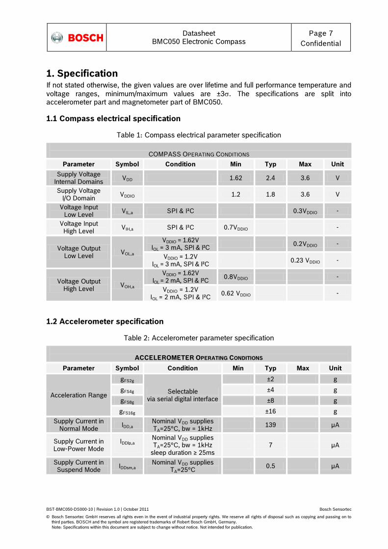
1. Specification If not stated otherwise, the given values are over lifetime and full performance temperature and
voltage ranges, minimum/maximum values are ±3. The specifications are split into accelerometer part and magnetometer part of BMC050.
1.1 Compass electrical specification
Table 1: Compass electrical parameter specification
COMPASS OPERATING CONDITIONS
Parameter Symbol Condition Min Typ Max Unit
Supply Voltage Internal Domains
VDD 1.62 2.4 3.6 V
Supply Voltage I/O Domain
VDDIO 1.2 1.8 3.6 V
Voltage Input Low Level
VIL,a SPI & I²C 0.3VDDIO -
Voltage Input High Level
VIH,a SPI & I²C 0.7VDDIO -
Voltage Output Low Level
VOL,a
VDDIO = 1.62V IOL = 3 mA, SPI & I²C
0.2VDDIO -
VDDIO = 1.2V IOL = 3 mA, SPI & I²C
0.23 VDDIO -
Voltage Output High Level
VOH,a
VDDIO = 1.62V IOL = 2 mA, SPI & I²C
0.8VDDIO -
VDDIO = 1.2V IOL = 2 mA, SPI & I²C
0.62 VDDIO -
1.2 Accelerometer specification
Table 2: Accelerometer parameter specification
ACCELEROMETER OPERATING CONDITIONS
Parameter Symbol Condition Min Typ Max Unit
Acceleration Range
gFS2g
Selectable via serial digital interface
±2 g
gFS4g ±4 g
gFS8g ±8 g
gFS16g ±16 g
Supply Current in Normal Mode
IDD,a Nominal VDD supplies TA=25°C, bw = 1kHz
139 µA
Supply Current in Low-Power Mode
IDDlp,a
Nominal VDD supplies TA=25°C, bw = 1kHz
sleep duration ≥ 25ms 7 µA
Supply Current in Suspend Mode
IDDsm,a Nominal VDD supplies
TA=25°C 0.5 µA
Datasheet
BMC050 Electronic Compass Page 8
Confidential
BST-BMC050-DS000-10 | Revision 1.0 | October 2011 Bosch Sensortec
© Bosch Sensortec GmbH reserves all rights even in the event of industrial property rights. We reserve all rights of disposal such as copying and passing on to
third parties. BOSCH and the symbol are registered trademarks of Robert Bosch GmbH, Germany.
Note: Specifications within this document are subject to change without notice. Not intended for publication.
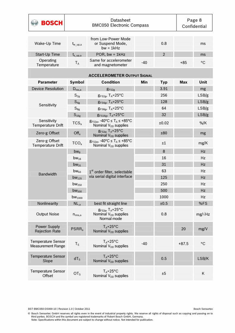
Wake-Up Time tw_up,a from Low-Power Mode
or Suspend Mode, bw = 1kHz
0.8 ms
Start-Up Time ts_up,a POR, bw = 1kHz 2 ms
Operating Temperature
TA Same for accelerometer
and magnetometer -40 +85 °C
ACCELEROMETER OUTPUT SIGNAL
Parameter Symbol Condition Min Typ Max Unit
Device Resolution Dres,a gFS2g 3.91 mg
Sensitivity
S2g gFS2g, TA=25°C 256 LSB/g
S4g gFS4g, TA=25°C 128 LSB/g
S8g gFS8g, TA=25°C 64 LSB/g
S16g gFS16g, TA=25°C 32 LSB/g
Sensitivity Temperature Drift
TCSa gFS2g, -40°C ≤ TA ≤ +85°C
Nominal VDD supplies ±0.02 %/K
Zero-g Offset Offa gFS2g, TA=25°C
Nominal VDD supplies ±80 mg
Zero-g Offset Temperature Drift
TCOa gFS2g, -40°C ≤ TA ≤ +85°C
Nominal VDD supplies ±1 mg/K
Bandwidth
bw8
1st order filter, selectable
via serial digital interface
8 Hz
bw16 16 Hz
bw31 31 Hz
bw63 63 Hz
bw125 125 Hz
bw250 250 Hz
bw500 500 Hz
bw1000 1000 Hz
Nonlinearity NL,a best fit straight line ±0.5 %FS
Output Noise nrms,a gFS2g, TA=25°C
Nominal VDD supplies Normal mode
0.8 mg/Hz
Power Supply Rejection Rate
PSRRa TA=25°C
Nominal VDD supplies 20 mg/V
Temperature Sensor Measurement Range
TS TA=25°C
Nominal VDD supplies -40 +87.5 °C
Temperature Sensor Slope
dTS TA=25°C
Nominal VDD supplies 0.5 LSB/K
Temperature Sensor Offset
OTS TA=25°C
Nominal VDD supplies ±5 K
Datasheet
BMC050 Electronic Compass Page 9
Confidential
BST-BMC050-DS000-10 | Revision 1.0 | October 2011 Bosch Sensortec
© Bosch Sensortec GmbH reserves all rights even in the event of industrial property rights. We reserve all rights of disposal such as copying and passing on to
third parties. BOSCH and the symbol are registered trademarks of Robert Bosch GmbH, Germany.
Note: Specifications within this document are subject to change without notice. Not intended for publication.
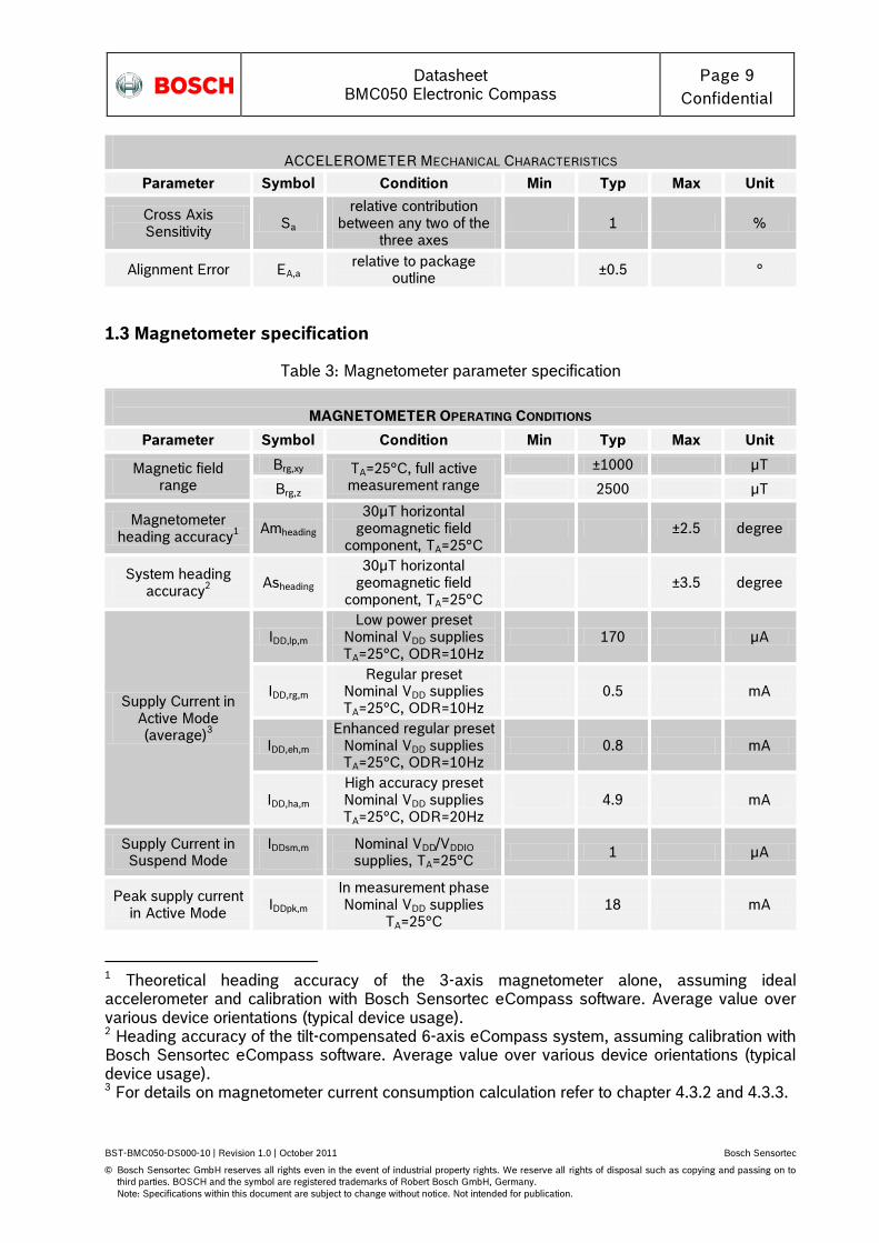
ACCELEROMETER MECHANICAL CHARACTERISTICS
Parameter Symbol Condition Min Typ Max Unit
Cross Axis Sensitivity
Sa relative contribution
between any two of the three axes
1 %
Alignment Error EA,a relative to package
outline ±0.5 °
1.3 Magnetometer specification
Table 3: Magnetometer parameter specification
MAGNETOMETER OPERATING CONDITIONS
Parameter Symbol Condition Min Typ Max Unit
Magnetic field range
Brg,xy TA=25°C, full active measurement range
±1000 µT
Brg,z 2500 µT
Magnetometer heading accuracy
1
Amheading 30µT horizontal
geomagnetic field component, TA=25°C
±2.5 degree
System heading accuracy
2
Asheading 30µT horizontal
geomagnetic field component, TA=25°C
±3.5 degree
Supply Current in Active Mode (average)
3
IDD,lp,m Low power preset
Nominal VDD supplies TA=25°C, ODR=10Hz
170 µA
IDD,rg,m Regular preset
Nominal VDD supplies TA=25°C, ODR=10Hz
0.5 mA
IDD,eh,m Enhanced regular preset
Nominal VDD supplies TA=25°C, ODR=10Hz
0.8 mA
IDD,ha,m High accuracy preset Nominal VDD supplies TA=25°C, ODR=20Hz
4.9 mA
Supply Current in Suspend Mode
IDDsm,m
Nominal VDD/VDDIO supplies, TA=25°C
1 µA
Peak supply current in Active Mode
IDDpk,m In measurement phase Nominal VDD supplies
TA=25°C 18 mA
1 Theoretical heading accuracy of the 3-axis magnetometer alone, assuming ideal accelerometer and calibration with Bosch Sensortec eCompass software. Average value over various device orientations (typical device usage). 2 Heading accuracy of the tilt-compensated 6-axis eCompass system, assuming calibration with Bosch Sensortec eCompass software. Average value over various device orientations (typical device usage). 3 For details on magnetometer current consumption calculation refer to chapter 4.3.2 and 4.3.3.

Datasheet
BMC050 Electronic Compass Page 10
Confidential
BST-BMC050-DS000-10 | Revision 1.0 | October 2011 Bosch Sensortec
© Bosch Sensortec GmbH reserves all rights even in the event of industrial property rights. We reserve all rights of disposal such as copying and passing on to
third parties. BOSCH and the symbol are registered trademarks of Robert Bosch GmbH, Germany.
Note: Specifications within this document are subject to change without notice. Not intended for publication.
Peak logic supply current in active
mode IDDIOpk,m
Only during measurement phase
Nominal VDDIO supplies TA=25°C
210 µA
POR time tw_up,m
from OFF to suspend; time starts when VDD>1.5V and VDDIO>1.1V
1.0 ms
Start-Up Time ts_up,m from suspend to sleep 3 ms
MAGNETOMETER OUTPUT SIGNAL
Parameter Symbol Condition Min Typ Max Unit
Device Resolution Dres,m TA=25°C (x,y,z) 0.3 µT
Sensitivity Sm After temperature compensation
TA=25°C Nominal VDD supplies
1 µT sensor output per µT applied
field
Sensitivity Temperature Drift
TCSm After temperature compensation
-40°C ≤ TA ≤ +85°C Nominal VDD supplies
±0.01 %/K
Zero-B offset OFFm TA=25°C ±10 µT
ODR (data output rate), normal mode
odrlp Low power preset 10 Hz
odrrg Regular preset 10 Hz
odreh Enhanced regular preset 10 Hz
odrha High accuracy preset 20 Hz
ODR (data output rate), forced mode
odrlp Low power preset 0 >300 Hz
odrrg Regular preset 0 100 Hz
odreh Enhanced regular preset 0 60 Hz
odrha High accuracy preset 0 20 Hz
Full-scale Nonlinearity
NLm, FS best fit straight line 1 %FS
Output Noise nrms,lp,m,xy Low power preset x-, y-axis, TA=25°C Nominal VDD supplies
1.0 µT
nrms,lp,m,z Low power preset z-axis, TA=25°C
Nominal VDD supplies
1.4 µT
nrms,rg,m Regular preset TA=25°C
Nominal VDD supplies
0.6 µT

Datasheet
BMC050 Electronic Compass Page 11
Confidential
BST-BMC050-DS000-10 | Revision 1.0 | October 2011 Bosch Sensortec
© Bosch Sensortec GmbH reserves all rights even in the event of industrial property rights. We reserve all rights of disposal such as copying and passing on to
third parties. BOSCH and the symbol are registered trademarks of Robert Bosch GmbH, Germany.
Note: Specifications within this document are subject to change without notice. Not intended for publication.
nrms,eh,m Enhanced regular preset TA=25°C
Nominal VDD supplies
0.5 µT
nrms,ha,m High accuracy preset TA=25°C
Nominal VDD supplies
0.3 µT
Power Supply Rejection Rate
PSRRm TA=25°C Nominal VDD supplies
±0.5 µT/V
Datasheet
BMC050 Electronic Compass Page 12
Confidential
BST-BMC050-DS000-10 | Revision 1.0 | October 2011 Bosch Sensortec
© Bosch Sensortec GmbH reserves all rights even in the event of industrial property rights. We reserve all rights of disposal such as copying and passing on to
third parties. BOSCH and the symbol are registered trademarks of Robert Bosch GmbH, Germany.
Note: Specifications within this document are subject to change without notice. Not intended for publication.
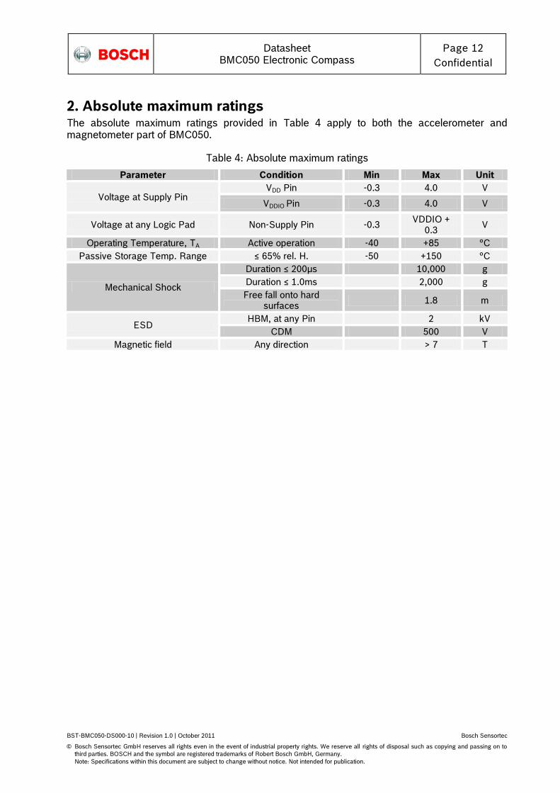
2. Absolute maximum ratings The absolute maximum ratings provided in Table 4 apply to both the accelerometer and magnetometer part of BMC050.
Table 4: Absolute maximum ratings
Parameter Condition Min Max Unit
Voltage at Supply Pin VDD Pin -0.3 4.0 V
VDDIO Pin -0.3 4.0 V
Voltage at any Logic Pad Non-Supply Pin -0.3 VDDIO +
0.3 V
Operating Temperature, TA Active operation -40 +85 °C
Passive Storage Temp. Range ≤ 65% rel. H. -50 +150 °C
Mechanical Shock
Duration ≤ 200µs 10,000 g
Duration ≤ 1.0ms 2,000 g
Free fall onto hard surfaces
1.8 m
ESD HBM, at any Pin 2 kV
CDM 500 V
Magnetic field Any direction > 7 T

Datasheet
BMC050 Electronic Compass Page 13
Confidential
BST-BMC050-DS000-10 | Revision 1.0 | October 2011 Bosch Sensortec
© Bosch Sensortec GmbH reserves all rights even in the event of industrial property rights. We reserve all rights of disposal such as copying and passing on to
third parties. BOSCH and the symbol are registered trademarks of Robert Bosch GmbH, Germany.
Note: Specifications within this document are subject to change without notice. Not intended for publication.
3. Block diagram Figure 1 shows the basic building blocks of the BMC050:
Figure 1: Block diagram of BMC050
X
Y
Z
M
U
X
Gain &
Offset
Logic
Vref
C/U ADC
Regulator
I
n
t
e
r
f
a
c
e
NVM Osc
VDD GND
VDDIO
PS1
INT1
INT2
SDI
SDO
SCK
CSB1
Accelerometer
MEMSAccelerometer ASIC
X
Y
X, Y
FlipCore
Drive &
Sense
Logic
Vref
Regulator
I
n
t
e
r
f
a
c
e
NVM Osc
VDD GND
VDDIO
PS2
INT3
DRDY
SDI
SDO
SCK
CSB2
FlipCores Magnetometer ASIC
Z Hall
element
Drive &
Sense
VDD
VDDIO
GND
PS1
INT1
INT2
SDI
SDO
SCK
CSB1
PS2
INT3
DRDY
CSB2
ADC
Datasheet
BMC050 Electronic Compass Page 14
Confidential
BST-BMC050-DS000-10 | Revision 1.0 | October 2011 Bosch Sensortec
© Bosch Sensortec GmbH reserves all rights even in the event of industrial property rights. We reserve all rights of disposal such as copying and passing on to
third parties. BOSCH and the symbol are registered trademarks of Robert Bosch GmbH, Germany.
Note: Specifications within this document are subject to change without notice. Not intended for publication.
4. Functional description BMC050 is a SiP (system in package) integration of a triaxial accelerometer (Sensing element and ASIC) and a triaxial geomagnetic sensor (Sensing element and ASIC) in one package. The two ASICs act as two separate slave devices on the digital bus (with different I²C address in I²C mode, or separate CSB lines in SPI mode, respectively), which allows an almost independent operation of accelerometer and magnetometer parts in order to fit into a wide range of usage scenarios. Note: Default values for registers can be found in chapters 5 and 6.
4.1 Power management
The BMC050 has two distinct power supply pins which supply both the acceleration sensor part and the magnetometer sensor part: • VDD is the main power supply for all internal analog and digital functional blocks; • VDDIO is a separate power supply pin, used for the supply of the digital interface as well as the magnetic sensor‟s logic. There are no limitations on the voltage levels of both pins relative to each other, as long as each of them lies within its operating range. Furthermore, the device can be completely switched off (VDD = 0V) while keeping the VDDIO supply on (VDDIO > 0V). To switch off the interface supply (VDDIO = 0V) and keep the internal supply on (VDD > 0V) is safe only in normal mode of the accelerometer part (magnetic sensor will switch to off mode automatically). If the accelerometer part of the device is in low-power mode or suspend mode while VDDIO = 0V, there is a risk of excess current consumption on the VDD supply (non-destructive). It is absolutely prohibited to keep any interface at a logical high level when VDDIO is switched off. Such a configuration will permanently damage the device (i.e. if VDDIO = 0 [SDI & SDO & SCK & CSB1 & CSB2] ≠ high). The device contains a power on reset (POR) generator for each of the sensor parts, accelerometer part and magnetometer part. It resets the logic part and the register values of the concerned ASIC after powering-on VDD and VDDIO. There is no limitation on the sequence of switching on both supply voltages. In case the I²C interface is used, a direct electrical connection between VDDIO supply and the PS pins (PS1 and PS2) is needed in order to ensure reliable protocol selection (see chapter 4.2).
4.2 Protocol selection
The BMC050 acts as two separate slave devices (i.e. accelerometer part and magnetometer part), on a digital interface (SPI or I²C) which is controlled by the external bus master (e.g. µC). The master obtains measurement data and status information from the device through the digital interface. In particular, the master can configure the interrupt controllers and read out the interrupt status registers. Moreover, it can freely configure and use the interrupt pins (INT1, INT2, INT3 and DRDY). All pads are in input mode (no output driver active) during the start-up sequence until the interface type is selected. The start-up sequence is run after power-up and after reset.

Datasheet
BMC050 Electronic Compass Page 15
Confidential
BST-BMC050-DS000-10 | Revision 1.0 | October 2011 Bosch Sensortec
© Bosch Sensortec GmbH reserves all rights even in the event of industrial property rights. We reserve all rights of disposal such as copying and passing on to
third parties. BOSCH and the symbol are registered trademarks of Robert Bosch GmbH, Germany.
Note: Specifications within this document are subject to change without notice. Not intended for publication.
Note: It is not possible to select mixed interfaces (I²C for accelerometer part and SPI for magnetometer part or vice versa), because the digital interface uses shared pins. Figure 2 illustrates the protocol selection:
Figure 2: Protocol selection
4.3 Power modes
The BMC050 features separately configurable power modes for the accelerometer and the magnetometer part. The advantage is that different characteristics regarding optimum system power saving of the two sensor types are exploited, and that the accelerometer part may also be used alone in certain usage scenarios where no magnetic field data is required. In such an example, the magnetometer part is able to suspend and save power during the time in which it is not required. In the following chapters, power modes for both accelerometer and magnetometer part are described.
4.3.1 Accelerometer power modes
The BMC050 accelerometer part has four different power modes (see Figure 4). Besides normal mode, which represents the fully operational state of the device, there are two special energy saving modes: low-power mode and suspend mode.
Reset (both accelerometer
and magnetometer)
Protocol
select
I²C operation SPI operation
One or more
interrupts can be
configured via I²C
One or more
interrupts can be
configured via SPI
PS1=PS2=GND
PS1=PS2=VDDIO
Datasheet
BMC050 Electronic Compass Page 16
Confidential
BST-BMC050-DS000-10 | Revision 1.0 | October 2011 Bosch Sensortec
© Bosch Sensortec GmbH reserves all rights even in the event of industrial property rights. We reserve all rights of disposal such as copying and passing on to
third parties. BOSCH and the symbol are registered trademarks of Robert Bosch GmbH, Germany.
Note: Specifications within this document are subject to change without notice. Not intended for publication.
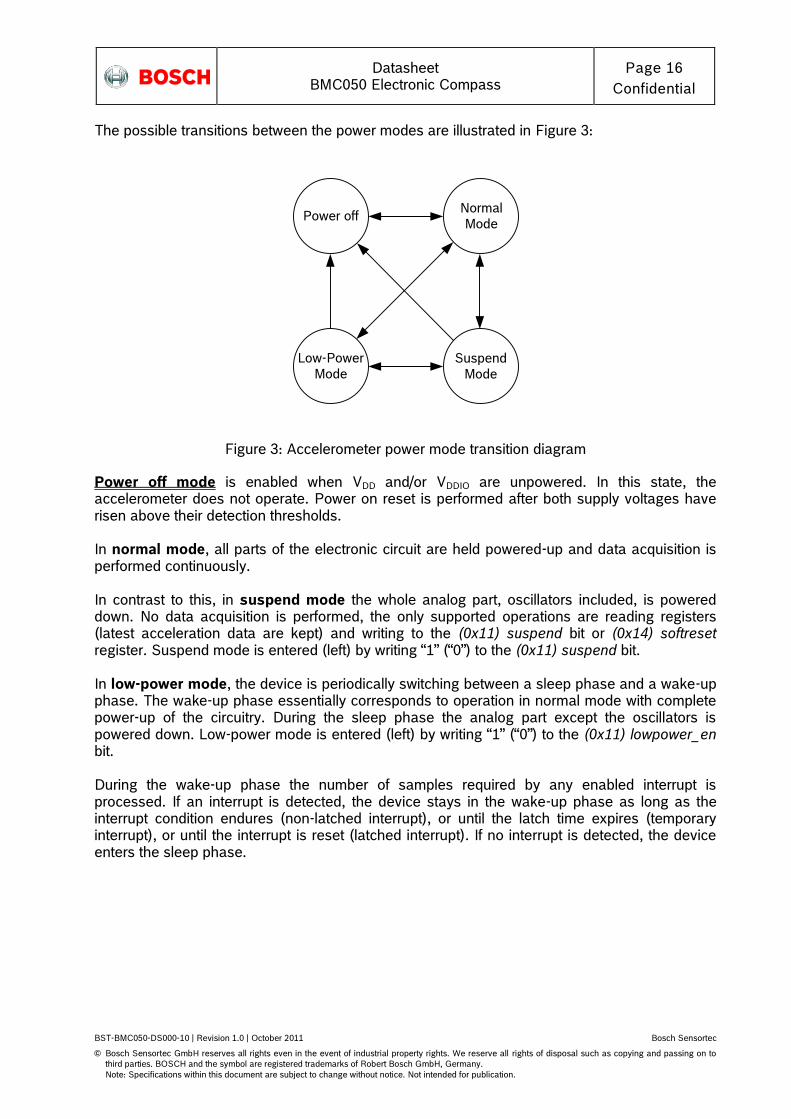
The possible transitions between the power modes are illustrated in Figure 3:
Low-Power
Mode
Suspend
Mode
Normal
ModePower off
Figure 3: Accelerometer power mode transition diagram
Power off mode is enabled when VDD and/or VDDIO are unpowered. In this state, the accelerometer does not operate. Power on reset is performed after both supply voltages have risen above their detection thresholds. In normal mode, all parts of the electronic circuit are held powered-up and data acquisition is performed continuously. In contrast to this, in suspend mode the whole analog part, oscillators included, is powered down. No data acquisition is performed, the only supported operations are reading registers (latest acceleration data are kept) and writing to the (0x11) suspend bit or (0x14) softreset register. Suspend mode is entered (left) by writing “1” (“0”) to the (0x11) suspend bit. In low-power mode, the device is periodically switching between a sleep phase and a wake-up phase. The wake-up phase essentially corresponds to operation in normal mode with complete power-up of the circuitry. During the sleep phase the analog part except the oscillators is powered down. Low-power mode is entered (left) by writing “1” (“0”) to the (0x11) lowpower_en bit. During the wake-up phase the number of samples required by any enabled interrupt is processed. If an interrupt is detected, the device stays in the wake-up phase as long as the interrupt condition endures (non-latched interrupt), or until the latch time expires (temporary interrupt), or until the interrupt is reset (latched interrupt). If no interrupt is detected, the device enters the sleep phase.
Datasheet
BMC050 Electronic Compass Page 17
Confidential
BST-BMC050-DS000-10 | Revision 1.0 | October 2011 Bosch Sensortec
© Bosch Sensortec GmbH reserves all rights even in the event of industrial property rights. We reserve all rights of disposal such as copying and passing on to
third parties. BOSCH and the symbol are registered trademarks of Robert Bosch GmbH, Germany.
Note: Specifications within this document are subject to change without notice. Not intended for publication.
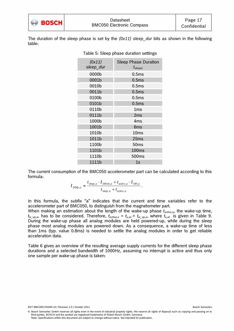
The duration of the sleep phase is set by the (0x11) sleep_dur bits as shown in the following table:
Table 5: Sleep phase duration settings
(0x11) sleep_dur
Sleep Phase Duration tsleepa
0000b 0.5ms
0001b 0.5ms
0010b 0.5ms
0011b 0.5ms
0100b 0.5ms
0101b 0.5ms
0110b 1ms
0111b 2ms
1000b 4ms
1001b 6ms
1010b 10ms
1011b 25ms
1100b 50ms
1101b 100ms
1110b 500ms
1111b 1s
The current consumption of the BMC050 accelerometer part can be calculated according to this formula:
aactiveasleep
aDDaactiveaDDsmasleep
aDDlptt
ItItI
,,
,,,,
,
.
In this formula, the subfix “a” indicates that the current and time variables refer to the accelerometer part of BMC050, to distinguish from the magnetometer part. When making an estimation about the length of the wake-up phase tactive,a, the wake-up time, tw_up,a, has to be considered. Therefore, tactive,a = tu,at + tw_up,a, where tu,at is given in Table 9. During the wake-up phase all analog modules are held powered-up, while during the sleep phase most analog modules are powered down. As a consequence, a wake-up time of less than 1ms (typ. value 0.8ms) is needed to settle the analog modules in order to get reliable acceleration data. Table 6 gives an overview of the resulting average supply currents for the different sleep phase durations and a selected bandwidth of 1000Hz, assuming no interrupt is active and thus only one sample per wake-up phase is taken:

Datasheet
BMC050 Electronic Compass Page 18
Confidential
BST-BMC050-DS000-10 | Revision 1.0 | October 2011 Bosch Sensortec
© Bosch Sensortec GmbH reserves all rights even in the event of industrial property rights. We reserve all rights of disposal such as copying and passing on to
third parties. BOSCH and the symbol are registered trademarks of Robert Bosch GmbH, Germany.
Note: Specifications within this document are subject to change without notice. Not intended for publication.
Table 6: Accelerometer part average current consumption in low-power mode
Sleep phase duration Average current consumption
0.5ms 100.5 µA
1ms 78.8 µA
2ms 55.0 µA
4ms 34.5 µA
6ms 25.2 µA
10ms 16.4 µA
25ms 7.4 µA
50ms 4.0 µA
100ms 2.3 µA
500ms 0.9 µA
1s 0.7 µA
4.3.2 Magnetometer power modes
The BMC050 magnetometer part has four power modes:
Power off mode
In Power off mode, VDD and/or VDDIO are unpowered. The magnetometer part does not operate in this mode. When only one of VDD or VDDIO is supplied, the magnetic sensor will still be in Power off mode. Power on reset is performed after both VDD and VDDIO have risen above their detection thresholds.
Suspend mode
Suspend mode is the default power mode of BMC050 magnetometer part after the chip is powered. When VDD and VDDIO are turned on the POR (power on reset) circuits operate and the device‟s registers are initialized. After POR becomes inactive, a start up sequence is executed. In this sequence NVM content is downloaded to shadow registers located in the device core. After the start up sequence the device is put in the Suspend mode. In this mode only registers supplied directly by VDDIO which store I2C slave device address, power control bit information and some others can be accessed by the user. No other registers can be accessed in Suspend mode. All registers lose their content, except the control register (0x4B). In particular, in this mode a Chip ID read (register 0x40) returns “0x00h” (I²C) or high-Z (SPI).
Sleep mode
The user puts device from suspend into Sleep mode by setting the Power bit to “1”, or from active modes (normal or forced) by setting OpMode bits to “11”. In this state the user has full access to the device registers. In particular, the Chip ID can be read. Setting the power control bit to “0” (register 0x4B bit0) will bring the device back into Suspend mode. From the Sleep mode the user can put the device back into Suspend mode or into Active mode.

Datasheet
BMC050 Electronic Compass Page 19
Confidential
BST-BMC050-DS000-10 | Revision 1.0 | October 2011 Bosch Sensortec
© Bosch Sensortec GmbH reserves all rights even in the event of industrial property rights. We reserve all rights of disposal such as copying and passing on to
third parties. BOSCH and the symbol are registered trademarks of Robert Bosch GmbH, Germany.
Note: Specifications within this document are subject to change without notice. Not intended for publication.
Active mode
The device can switch into Active mode from Sleep mode by setting OpMode bits (register 0x4C). In active mode the magnetic field measurements are performed. In active mode, all registers are accessible. In active mode, two operation modes can be distinguished:
Normal mode: selected channels are periodically measured according to settings set in user registers. After measurements are completed, output data is put into data registers and the device waits for the next measurement period, which is set by programmed output data rate (ODR). From normal mode, the user can return to sleep mode by setting OpMode to “11” or by performing a soft reset (see chapter 6.6). Suspend mode can be entered by setting power control bit to “0”.
Forced mode (single measurement): When set by the host, the selected channels are measured according to settings programmed in user registers. After measurements are completed, output data is put into data registers, OpMode register value returns to “11” and the device returns to sleep mode. The forced mode is useful to achieve synchronized operation between host microcontroller and BMC050. Also, different data output rates from the ones selectable in normal mode can be achieved using forced mode.
Figure 4: Magnetometer power mode transition diagram
In Active Mode and normal operation, in principle any desired balance between output noise and active time (hence power consumption) can be adjusted by the repetition settings for x/y-axis and z-axis and the output data rate ODR. The average power consumption depends on the ratio of high current phase time (during data acquisition) and low current phase time (between data acquisitions). Hence, the more repetitions are acquired to generate one magnetic field data point, the longer the active time ratio in one sample phase, and the higher the average current. Thanks to longer internal averaging, the noise level of the output data reduces with increasing number of repetitions.

Datasheet
BMC050 Electronic Compass Page 20
Confidential
BST-BMC050-DS000-10 | Revision 1.0 | October 2011 Bosch Sensortec
© Bosch Sensortec GmbH reserves all rights even in the event of industrial property rights. We reserve all rights of disposal such as copying and passing on to
third parties. BOSCH and the symbol are registered trademarks of Robert Bosch GmbH, Germany.
Note: Specifications within this document are subject to change without notice. Not intended for publication.
By using forced mode, it is possible to trigger new measurements at any rate. The user can therefore trigger measurements in a shorter interval than it takes for a measurement cycle to complete. If a measurement cycle is not allowed to complete, the resulting data will not be written into the data registers. To prevent this, the manually triggered measurement intervals must not be shorter than the active measurement time which is a function of the selected number of repetitions. The maximum selectable read-out frequency in forced mode can be calculated as follows:
µsnZµsnXYµsf ODR
980500145
1max,
Hereby nXY is the number of repetitions on X/Y-axis (not the register value) and nZ the number of repetitions on Z-axis (not the register value) (see description of XY_REP and Z_REP registers in chapter 6). Although the repetition numbers for X/Y and Z axis and the ODR can be adjusted independently and in a wide range, there are four recommended presets (High accuracy preset, Enhanced regular preset, Regular preset, Low power preset) which reflect the most common usage scenarios, i.e. required output accuracy at a given current consumption, of the BMC050 magnetometer part. The three presets consist of the below register configurations, which are automatically set by the BMC050 API or driver provided by Bosch Sensortec when a preset is selected. Table 7 shows the recommended presets and the resulting magnetic field output noise and magnetometer part current consumption:
Table 7: Magnetometer presets in Active operation and normal mode:
Preset X/Y rep Z rep ODR ODRmax (forced mode)
RMS Noise x/y/z
Average current
consumption
Low power preset
3 3 10 Hz >300 Hz 1.0/1.0/1.4
µT 170 µA
Regular preset 9 15 10 Hz 100 Hz 0.6/0.6/0.6
µT 0.5 mA
Enhanced regular preset
15 27 10 Hz 60 Hz 0.5/0.5/0.5
µT 0.8 mA
High accuracy preset
47 83 20 Hz 20 Hz 0.3/0.3/0.3
µT 4.9 mA

Datasheet
BMC050 Electronic Compass Page 21
Confidential
BST-BMC050-DS000-10 | Revision 1.0 | October 2011 Bosch Sensortec
© Bosch Sensortec GmbH reserves all rights even in the event of industrial property rights. We reserve all rights of disposal such as copying and passing on to
third parties. BOSCH and the symbol are registered trademarks of Robert Bosch GmbH, Germany.
Note: Specifications within this document are subject to change without notice. Not intended for publication.
4.3.3 BMC050 overall power consumption
Below, Table 8 shows the overall current consumption of BMC050 (sum of accelerometer and magnetometer part) in typical scenarios such as a tilt-compensated electronic compass application.
Table 8: BMC050 overall current consumption in typical usage scenarios:
Compass preset
Acc. Active / sleep
interval
Mag. DOR
Acc. BW / DOR
Mag. avg. current
Acc. avg. current
Total average current
Low power preset
8 / 50 ms 10 Hz 62.5 / 17
Hz 170 µA 20 µA 190 µA
Regular preset
16 / 50 ms 10 Hz 31 / 15
Hz 0.5 mA 35 µA 0.54 mA
Enhanced regular preset
16 / 50 ms 10 Hz 31 / 15
Hz 0.8 mA 35 µA 0.84 mA
High accuracy preset
16 /25 ms 20 Hz 31 / 24
Hz 4.9 mA 55 µA 5.0 mA
4.4 Sensor data
4.4.1 Acceleration data
The width of acceleration data is 10 bits given in two´s complement representation. The 10 bits for each axis are split into an MSB upper part (one byte containing bits 9 to 2) and an LSB lower part (one byte containing bits 1 and 0 of acceleration and a (0x02, 0x04, 0x06) new_data flag). Reading the acceleration data registers shall always start with the LSB part. The content of an MSB register is updated by reading the corresponding LSB register (shadowing procedure). The shadowing procedure can be disabled (enabled) by writing “1” (“0”) to the bit shadow_dis. With disabled shadowing, the content of both MSB and LSB registers is updated by a new value immediately. Unused bits of the LSB registers are fixed to 0. The (0x02, 0x04, 0x06) new_data flag of each LSB register is set if the data registers are updated, it is reset if either the corresponding MSB or LSB part is read. Two different streams of acceleration data are available, unfiltered and filtered. The unfiltered data is sampled with 2kHz. The sampling rate of the filtered data depends on the selected filter bandwidth; it is twice the bandwidth. Which kind of data is stored in the acceleration data registers depends on bit (0x13) data_high_bw. If (0x13) data_high_bw is “0” (“1”), then filtered (unfiltered) data is stored in the registers. Both data streams are separately offset-compensated. Both kinds of data can be processed by the interrupt controller.

Datasheet
BMC050 Electronic Compass Page 22
Confidential
BST-BMC050-DS000-10 | Revision 1.0 | October 2011 Bosch Sensortec
© Bosch Sensortec GmbH reserves all rights even in the event of industrial property rights. We reserve all rights of disposal such as copying and passing on to
third parties. BOSCH and the symbol are registered trademarks of Robert Bosch GmbH, Germany.
Note: Specifications within this document are subject to change without notice. Not intended for publication.
The bandwidth of filtered acceleration data is determined by setting the (0x10) bw bit as follows:
Table 9: Bandwidth configuration
bw Bandwidth Update Time
tut
00xxx *) -
01000 7.81Hz 64ms
01001 15.63Hz 32ms
01010 31.25Hz 16ms
01011 62.5Hz 8ms
01100 125Hz 4ms
01101 250Hz 2ms
01110 500Hz 1ms
01111 1000Hz 0.5ms
1xxxx *) -
*) Note: Settings 00xxx result in a bandwidth of 7.81 Hz; settings 1xxxx result in a bandwidth of 1000 Hz. It is recommended to actively use the range from “01000b” to “01111b” only in order to be compatible with future products.

Datasheet
BMC050 Electronic Compass Page 23
Confidential
BST-BMC050-DS000-10 | Revision 1.0 | October 2011 Bosch Sensortec
© Bosch Sensortec GmbH reserves all rights even in the event of industrial property rights. We reserve all rights of disposal such as copying and passing on to
third parties. BOSCH and the symbol are registered trademarks of Robert Bosch GmbH, Germany.
Note: Specifications within this document are subject to change without notice. Not intended for publication.
The BMC050‟s accelerometer part supports four different acceleration measurement ranges. A measurement range is selected by setting the (0x0F) range bits as follows:
Table 10: Range selection
Range Acceleration measurement
range
Resolution
0011 ±2g 3.91mg/LSB
0101 ±4g 7.81mg/LSB
1000 ±8g 15.62mg/LSB
1100 ±16g 31.25mg/LSB
others reserved -
4.4.2 Temperature data
The width of temperature data is 8 bits given in two´s complement representation. Temperature values are available in the (0x08) temp register. The slope of the temperature sensor is 0.5K/LSB, its center temperature is 24°C [(0x08) temp = 0x00]. Therefore, the typical temperature measurement range is -40°C up to 87.5°C.
4.4.3 Magnetic field data
The representation of magnetic field data is different between X/Y-axis and Z-axis. The width of X- and Y-axis magnetic field data is 13 bits each and stored in two‟s complement. DATAX_LSB (0x42) contains 5-bit LSB part [4:0] of the 13 bit output data of the X-channel. DATAX_MSB (0x43) contains 8-bit MSB part [12:5] of the 13 bit output data of the X-channel. DATAY_LSB (0x44) contains 5-bit LSB part [4:0] of the 13 bit output data of the Y-channel. DATAY_MSB (0x45) contains 8-bit MSB part [12:5] of the 13 bit output data of the Y-channel. The width of the Z-axis magnetic field data is 15 bit word stored in two‟s complement. DATAZ_LSB (0x46) contains 7-bit LSB part [6:0] of the 15 bit output data of the Z-channel. DATAZ_MSB (0x47) contains 8-bit MSB part [14:7] of the 15 bit output data of the Z-channel. For all axes, temperature compensation on the host is used to get ideally matching sensitivity over the full temperature range. The temperature compensation is based on a resistance measurement of the hall sensor plate. The resistance value is represented by a 14 bit unsigned output word. RHALL_LSB (0x48) contains 6-bit LSB part [5:0] of the 14 bit output data of the RHALL-channel. RHALL_MSB (0x49) contains 8-bit MSB part [13:6] of the 14 bit output data of the RHALL-channel. All signed register values are in two´s complement representation. Bits which are marked “reserved” can have different values or can in some cases not be read at all (read will return 0x00 in I²C mode and high-Z in SPI mode). Data register readout and shadowing is implemented as follows: After all enabled axes have been measured, complete data packages consisting of DATAX, DATAY, DATAZ and RHALL are updated at once in the data registers. This way, it is prevented

Datasheet
BMC050 Electronic Compass Page 24
Confidential
BST-BMC050-DS000-10 | Revision 1.0 | October 2011 Bosch Sensortec
© Bosch Sensortec GmbH reserves all rights even in the event of industrial property rights. We reserve all rights of disposal such as copying and passing on to
third parties. BOSCH and the symbol are registered trademarks of Robert Bosch GmbH, Germany.
Note: Specifications within this document are subject to change without notice. Not intended for publication.
that a following axis is updated while the first axis is still being read (axis mix-up) or that MSB part of an axis is updated while LSB part is being read. While reading from any data register, data register update is blocked. Instead, incoming new data is written into shadow registers which will be written to data registers after the previous read sequence is completed (i.e. upon stop condition in I²C mode, or CSB going high in SPI mode, respectively). Hence, it is recommended to read out at all data at once (0x42 to 0x49 or 0x4A if status bits are also required) with a burst read. Single bytes or axes can be read out, while in this case it is not assured that adjacent registers are not updated during readout sequence. The “Data ready status” bit (register 0x48 bit0) is set “1” when the data registers have been updated but the data was not yet read out over digital interface. Data ready is cleared (set “0”) directly after completed read out of any of the data registers and subsequent stop condition (I²C) or lifting of CSB (SPI). In addition, when enabled the “Data overrun” bit (register 0x4A bit7) turns “1” whenever data registers are updated internally, but the old data was not yet read out over digital interface (i.e. data ready bit was still high). The “Data overrun” bit is cleared when the interrupt status register 0x4A is read out. This function needs to be enabled separately by setting the “Data overrun En” bit (register 0x4D bit7)). Note: Please also see chapter 6 for detailed register descriptions.

Datasheet
BMC050 Electronic Compass Page 25
Confidential
BST-BMC050-DS000-10 | Revision 1.0 | October 2011 Bosch Sensortec
© Bosch Sensortec GmbH reserves all rights even in the event of industrial property rights. We reserve all rights of disposal such as copying and passing on to
third parties. BOSCH and the symbol are registered trademarks of Robert Bosch GmbH, Germany.
Note: Specifications within this document are subject to change without notice. Not intended for publication.
4.4.4 Magnetic field data temperature compensation
The raw register values DATAX, DATAY, DATAZ and RHALL are read out from the host processor using the BMC050 API/driver which is provided by Bosch Sensortec. The API/driver performs an off-chip temperature compensation and outputs x/y/z magnetic field data in 16 LSB/µT to the upper application layer:
Figure 5: Calculation flow of magnetic field data from raw BMC050 register data
The API/driver performs all calculations using highly optimized fixed-point C-code arithmetic. For platforms that do not support C code, a floating-point formula is available as well.
BMC050
sensorHardware level
Software
driver level
BMC050
API / driver(provided by
Bosch Sensortec)
ApplicationSoftware
application level
Magnetometer raw register data
(DATAX, DATAY, DATAZ, RHALL)
Temperature compensated
magnetic field data x/y/z in
(signed short int, 16 LSB/µT)
Config
Configa
a
Datasheet
BMC050 Electronic Compass Page 26
Confidential
BST-BMC050-DS000-10 | Revision 1.0 | October 2011 Bosch Sensortec
© Bosch Sensortec GmbH reserves all rights even in the event of industrial property rights. We reserve all rights of disposal such as copying and passing on to
third parties. BOSCH and the symbol are registered trademarks of Robert Bosch GmbH, Germany.
Note: Specifications within this document are subject to change without notice. Not intended for publication.
4.5 Self-test
4.5.1 Accelerometer self-test
This feature permits to check the BMC050‟s accelerometer part functionality by applying electrostatic forces to the sensor core instead of external accelerations. By actually deflecting the seismic mass, the entire signal path of the sensor can be tested. Activating the self-test results in a static offset of the acceleration data; any external acceleration or gravitational force applied to the sensor during active self-test will be observed in the output as a superposition of both acceleration and self-test signal. The self-test is activated individually for each axis by writing the proper value to the (0x32) self_test_axis bits (“01b” for x-axis, “10b” for y-axis, “11b” for z-axis, “00b” to deactivate self-test). It is possible to control the direction of the deflection through bit (0x32) self_test_sign. The excitation occurs in positive (negative) direction if (0x32) self_test_sign = “0” (“1”). In order to ensure a proper interpretation of the self-test signal it is recommended to perform the self-test for both (positive and negative) directions and then to calculate the difference of the resulting acceleration values. Table 11 shows the minimum differences for each axis. The actually measured signal differences can be significantly larger.
Table 11: Self-test difference values
x-axis signal y-axis signal z-axis signal
resulting minimum
difference signal
+0.8 g
+0.8 g
+0.4 g
It is recommended to perform a reset of the device after self-test. If the reset cannot be performed, the following sequence must be kept to prevent unwanted interrupt generation:
disable interrupts, change parameters of interrupts, wait for at least 600 s, enable desired interrupts.
4.5.2 Magnetometer self-test
BMC050 supports two self-tests modes for the magnetometer part: Normal self-test and advanced self-test.
Normal self test
During normal self-test, the following verifications are performed:
FlipCore signal path is verified by generating signals on-chip. These are processed through the signal path and the measurement result is compared to known thresholds.
FlipCore (X and Y) bondwires to ASIC are checked for connectivity
FlipCore (X and Y) bondwires and MEMS are checked for shorts
Hall sensor connectivity is checked for open and shorted connections
Hall sensor signal path and hall sensor element offset are checked for overflow. To perform a self test, the sensor must first be put into sleep mode (OpMode = “11”). Self-test mode is then entered by setting the bit “Self test” (register 0x4C bit0) to “1”. After performing self

Datasheet
BMC050 Electronic Compass Page 27
Confidential
BST-BMC050-DS000-10 | Revision 1.0 | October 2011 Bosch Sensortec
© Bosch Sensortec GmbH reserves all rights even in the event of industrial property rights. We reserve all rights of disposal such as copying and passing on to
third parties. BOSCH and the symbol are registered trademarks of Robert Bosch GmbH, Germany.
Note: Specifications within this document are subject to change without notice. Not intended for publication.
test, this bit is set back to “0”. When self-test is successful, the corresponding self-test result bits are set to “1” (“X-Self-Test” register 0x42 bit0, “Y-Self-Test” register 0x44 bit0, “Z-Self-Test” register 0x46 bit0). If self-test fails for an axis, the corresponding result bit returns “0”.
Advanced self test
Advanced self test performs a verification of the Z channel signal path functionality and sensitivity. An on-chip coil wound around the hall sensor can be driven in both directions with a calibrated current to generate a positive or negative field of around 100 µT. Advanced self test is an option that is active in parallel to the other operation modes. The only difference is that during the active measurement phase, the coil current is enabled. The recommended usage of advanced self test is the following:
1. Set sleep mode 2. Disable X, Y axis 3. Set Z repetitions to desired level 4. Enable positive advanced self test current 5. Set forced mode, readout Z and R channel after measurement is finished 6. Enable negative advanced self test current 7. Set forced mode, readout Z and R channel after measurement is finished 8. Disable advanced self test current (this must be done manually) 9. Calculate difference between the two compensated field values. This difference should
be around 200 µT with some margins. 10. Perform a soft reset of manually restore desired settings
Please refer to the corresponding application note for the exact thresholds to evaluate advanced self-test. Below table describes how the advanced self-test is controlled:
Table 12: Magnetometer advanced self-test control
(0x4C) Adv.ST <1:0>
Configuration
00b Normal operation
(no self-test), default
01b Reserved, do not use
10b Negative on-chip magnetic
field generation
11b Positive on-chip magnetic
field generation The BMC050 API/driver provided by Bosch Sensortec provides a comfortable way to perform both self-tests and to directly obtain the result without further calculations. It is recommended to use this as a reference.

Datasheet
BMC050 Electronic Compass Page 28
Confidential
BST-BMC050-DS000-10 | Revision 1.0 | October 2011 Bosch Sensortec
© Bosch Sensortec GmbH reserves all rights even in the event of industrial property rights. We reserve all rights of disposal such as copying and passing on to
third parties. BOSCH and the symbol are registered trademarks of Robert Bosch GmbH, Germany.
Note: Specifications within this document are subject to change without notice. Not intended for publication.
4.6 Accelerometer offset compensation
Offsets in measured acceleration signals can have several causes but they are always unwanted and disturbing in many cases. Therefore, the BMC050 offers an advanced set of four digital offset compensation methods which are closely matched to each other. These are slow, fast, and manual compensation, and inline calibration. The compensation is performed for unfiltered and filtered acceleration data independently. It is done by adding a compensation value to the acceleration data coming from the ADC. The result of this computation is saturated if necessary to prevent any overflow errors (the smallest or biggest possible value is set, depending on the sign). However, the public registers used to read and write compensation values have only a width of 8 bits. An overview of the offset compensation principle is given in Figure 6:
Figure 6: Principle of offset compensation
The meaning of both public and internal registers is the same for all acceleration measurement ranges. Therefore, with measurement ranges other than ±2g, one or more lower significant bits of the internal registers are lost when added to an acceleration value, or are set to zero when the internal compensation value is computed. If a compensation value is too small or too big to fit into the corresponding internal register, it is saturated to prevent an overflow error. In a similar way the conversion of the internal register value to the public register value (10bit to 8bit) uses saturation.
bit_11
bit_12
bit_10
bit_9
bit_8
bit_7
bit_6
bit_5
bit_4
bit_3
bit_2
bit_1
bit_0
sign (msb)
62.5mg
31.3mg
15.6mg
7.8mg (lsb)
125mg
250mg
500mg
sign (msb)
62.5mg
31.3mg
15.6mg
7.8mg
3.9mg (lsb)
125mg
250mg
500mg
1g
8bit – 10bit
conversion
sign (msb)
62.5mg
31.3mg
15.6mg
7.8mg
125mg
250mg
500mg
1g
2gsign (msb)
62.5mg
31.3mg
15.6mg
7.8mg
3.9mg
125mg
250mg
500mg
1g
sign (msb)
62.5mg
31.3mg
15.6mg
125mg
250mg
500mg
1g
2g
4g
sign (msb)
62.5mg
31.3mg
125mg
250mg
500mg
1g
2g
4g
8g
acceleration data
range: ±2g ±16g±4g ±8g
offset_filt_full_x/y/z
or
offset_unfilt_x/y/z
(10bit)
internal register
offset_filt_x/y/z
or
offset_unfilt_x/y/z
(8bit)
public register
add to
compute compensation value
a
a

Datasheet
BMC050 Electronic Compass Page 29
Confidential
BST-BMC050-DS000-10 | Revision 1.0 | October 2011 Bosch Sensortec
© Bosch Sensortec GmbH reserves all rights even in the event of industrial property rights. We reserve all rights of disposal such as copying and passing on to
third parties. BOSCH and the symbol are registered trademarks of Robert Bosch GmbH, Germany.
Note: Specifications within this document are subject to change without notice. Not intended for publication.
Summarized, in dependence to the measurement range which has been set, the compensation value, which has been written into the public register will correct the data output according to Figure 6. e.g. ±2g range: public register = 00000001b add to acceleration data = ±7.8mg = +2LSB public register = 00000010b add to acceleration data = +15.6mg = +4LSB public register = 00000101b add to acceleration data = +39.1mg = +10LSB The public registers are image registers of EEPROM registers. With each image update (see chapter 4.7 for details) the contents of the non-volatile EEPROM registers are written to the public registers. At any time the public register can be over-written by the user. After changing the contents of the public registers by either an image update or manually, all 8bit values are widened to 10bit values and stored in the corresponding internal registers. In the opposite direction, if the value of an internal register changes due to the computation performed by a compensation algorithm, it is converted to an 8bit value and stored in the public register. For slow and fast offset compensation, the compensation target can be chosen by setting the bits (0x37) offset_target_x, (0x37) offset_target_y, and (0x37) offset_target_z according to Table 13:
Table 13: Offset target settings
(0x37) offset_target_x/y/z
Target value
00b 0g
01b +1g
10b -1g
11b 0g By writing “1” to the (0x36) offset_reset bit, all offset compensation registers are reset to zero.
4.6.1 Slow compensation
Slow compensation is a quasi-continuous process which regulates the acceleration value of each axis towards the target value by comparing the current value with the target and adding or subtracting a fixed value depending on the comparison. The algorithm in detail: If an acceleration value is larger (smaller) than the target value (0x37) offset_target_x/y/z for a number of samples (given by the parameter Offset Period, see Table 14), the internal offset compensation value (0x38, 0x39, 0x3A) offset_filt_x/y/z or (0x3B, 0x03C, 0x3D) offset_unfilt_x/y/z is decremented (incremented) by 4 LSB. The public registers (0x38, 0x39, 0x3A) offset_filt_x/y/z and (0x3B, 0x03C, 0x3D) offset_unfilt_x/y/z are not used for the computations but they are updated with the contents of the internal registers (using saturation if necessary) and can be read by the user.

Datasheet
BMC050 Electronic Compass Page 30
Confidential
BST-BMC050-DS000-10 | Revision 1.0 | October 2011 Bosch Sensortec
© Bosch Sensortec GmbH reserves all rights even in the event of industrial property rights. We reserve all rights of disposal such as copying and passing on to
third parties. BOSCH and the symbol are registered trademarks of Robert Bosch GmbH, Germany.
Note: Specifications within this document are subject to change without notice. Not intended for publication.
The compensation period offset_period is set by the (0x37) cut_off bit as represented in Table 14:
Table 14: Compensation period settings
(0x37) cut_off
Offset Period
0b 8
1b 16 The slow compensation can be enabled (disabled) for each axis independently by setting the bits (0x36) hp_x_en, hp_y_en, hp_z_en to “1” (“0”), respectively. Slow compensation should not be used in combination with low-power mode. In low-power mode the conditions (availability of necessary data) for proper function of slow compensation are not fulfilled.
4.6.2 Fast compensation
Fast compensation is a one-shot process by which the compensation value is set in such a way that when added to the raw acceleration, the resulting acceleration value of each axis equals the target value. The algorithm in detail: An average of 16 consecutive acceleration values is computed and the difference between target value and computed value is written to (0x38, 0x39, 0x3A) offset_filt_x/y/z or (0x3B, 0x3C, 0x3D) offset_unfilt_x/y/z The public registers (0x38, 0x39, 0x3A) offset_filt_x/y/z and (0x3B, 0x3C, 0x3D) offset_unfilt_x/y/z are updated with the contents of the internal registers (using saturation if necessary) and can be read by the user. Fast compensation is triggered for each axis individually by setting the (0x36) cal_trigger bits as shown in Table 15:
Table 15: Fast compensation axis selection
(0x36) cal_trigger
Selected Axis
00b none
01b x
10b y
11b z The register (0x36) cal_trigger keeps its non-zero value while the fast compensation procedure is running. Slow compensation is blocked as long as fast compensation endures. Bit (0x36) cal_rdy is “0” when (0x36) cal_trigger is not “00”. Fast compensation should not be used in combination with low-power mode. In low-power mode the conditions (availability of necessary data) for proper function of fast compensation are not fulfilled.

Datasheet
BMC050 Electronic Compass Page 31
Confidential
BST-BMC050-DS000-10 | Revision 1.0 | October 2011 Bosch Sensortec
© Bosch Sensortec GmbH reserves all rights even in the event of industrial property rights. We reserve all rights of disposal such as copying and passing on to
third parties. BOSCH and the symbol are registered trademarks of Robert Bosch GmbH, Germany.
Note: Specifications within this document are subject to change without notice. Not intended for publication.
4.6.3 Manual compensation
As explained above, the contents of the public compensation registers (0x38, 0x39, 0x3A) offset_filt_x/y/z and (0x3B, 0x3C, 0x3D) offset_unfilt_x/y/z can be set manually via the digital interface. It is recommended to write into these registers immediately after a new data interrupt in order not to disturb running offset computations. Writing to the offset compensation registers is not allowed if slow compensation is enabled or if the fast compensation procedure is running.
4.6.4 Inline calibration
For a given application, it is often desirable to calibrate the offset once and to store the compensation values permanently. This can be achieved by using one of the aforementioned offset compensation methods to determine the proper compensation values and then storing these values permanently in the non-volatile memory (EEPROM). See chapter 4.7 for details of the storing procedure. Each time the device is reset, the compensation values are loaded from the non-volatile memory into the image registers and used for offset compensation until they are possibly overwritten using one of the other compensation methods.
Datasheet
BMC050 Electronic Compass Page 32
Confidential
BST-BMC050-DS000-10 | Revision 1.0 | October 2011 Bosch Sensortec
© Bosch Sensortec GmbH reserves all rights even in the event of industrial property rights. We reserve all rights of disposal such as copying and passing on to
third parties. BOSCH and the symbol are registered trademarks of Robert Bosch GmbH, Germany.
Note: Specifications within this document are subject to change without notice. Not intended for publication.
4.7 Non-volatile memory
4.7.1 Accelerometer non-volatile memory
The memory of the accelerometer part of BMC050 consists of three different kinds of registers: hard-wired, volatile, and non-volatile. Non-volatile memory is implemented as EEPROM. Part of it can be both read and written by the user. Access to non-volatile memory is only possible through (volatile) image registers. Altogether, there are eight registers (bytes) of EEPROM which are accessible by the customer. The address range of the image registers range from 0x38 to 0x3F. While the addresses up to 0x3D are used for offset compensation (see 4.6 Offset Compensation), addresses 0x3E and 0x3F are general purpose registers not linked to any sensor-specific functionality. The content of the EEPROM is loaded to the image registers after a reset (either POR or softreset) or after a user request which is performed by writing “1” to bit (0x33) nvm_load. As long as the image update is not yet complete, bit (0x33) nvm_load is “1”, otherwise it is “0”. The image registers can be read and written like any other register. Writing to the EEPROM is a three-step procedure:
1. Write the new contents to the image registers. 2. Write “1” to bit (0x33) nvm_prog_mode in order to unlock the EEPROM. 3. Write “1” to bit (0x33) nvm_prog_trig and keep “1” in bit (0x33) nvm_prog_mode in order
to trigger the write process. Writing to the EEPROM always renews the entire EEPROM contents. It is possible to check the write status by reading bit (0x33) nvm_rdy. While (0x33) nvm_rdy = “0”, the write process is still enduring; if (0x33) nvm_rdy = “1”, then writing is completed. As long as the write process is ongoing, no power mode change and no image update is allowed. It is forbidden to write to the EEPROM while the image update is running, in low-power mode, and in suspend mode.
4.7.2 Magnetometer non-volatile memory
Some of the memory of the BMC050 magnetometer is non-volatile memory (NVM). This NVM is pre-programmed in Bosch Sensortec fabrication line and can not be modified afterwards. It contains trimming data which are required for sensor operation and sensor data compensation, thus it is read out by the BMC050 API/driver during initialization.

Datasheet
BMC050 Electronic Compass Page 33
Confidential
BST-BMC050-DS000-10 | Revision 1.0 | October 2011 Bosch Sensortec
© Bosch Sensortec GmbH reserves all rights even in the event of industrial property rights. We reserve all rights of disposal such as copying and passing on to
third parties. BOSCH and the symbol are registered trademarks of Robert Bosch GmbH, Germany.
Note: Specifications within this document are subject to change without notice. Not intended for publication.
4.8 Accelerometer interrupt controller
Seven accelerometer based interrupt engines are integrated in the accelerometer part of BMC050. Each interrupt can be independently enabled and configured. If the condition of an enabled interrupt is fulfilled, the corresponding status bit is set to “1” and the selected interrupt pin is activated. There are two interrupt pins for the accelerometer part, INT1 and INT2; interrupts can be freely mapped to any of these pins. The pin state is a logic ´or´ combination of all mapped interrupts. The interrupt status registers are updated together with writing new data into the acceleration data registers. If an interrupt is disabled, all active status bits and pins are immediately reset. All time constants are based upon the typical frequency of the internal oscillator. This is reflected by the bandwidths (bw) as specified in Table 9.
4.8.1 General features
An interrupt is cleared depending on the selected interrupt mode, which is common to all interrupts. There are three different interrupt modes for the accelerometer part: non-latched, latched, and temporary. The mode is selected by the (0x21) latch_int bits according to Table 16.
Table 16: Accelerometer interrupt mode selection
(0x21) latch_int
Interrupt mode
0000b non-latched
0001b temporary, 250ms
0010b temporary, 500ms
0011b temporary, 1s
0100b temporary, 2s
0101b temporary, 4s
0110b temporary, 8s
0111b latched
1000b non-latched
1001b temporary, 500µs
1010b temporary, 500µs
1011b temporary, 1ms
1100b temporary, 12.5ms
1101b temporary, 25ms
1110b temporary, 50ms
1111b latched An interrupt is generated if its activation condition is met. It can not be cleared as long as the activation condition is fulfilled. In the non-latched mode the interrupt status bit and the selected pin (the contribution to the ´or´ condition for INT1 and/or INT2) are cleared as soon as the activation condition is no more valid. Exceptions to this behaviour are the new data, orientation, and flat interrupts, which are automatically reset after a fixed time.
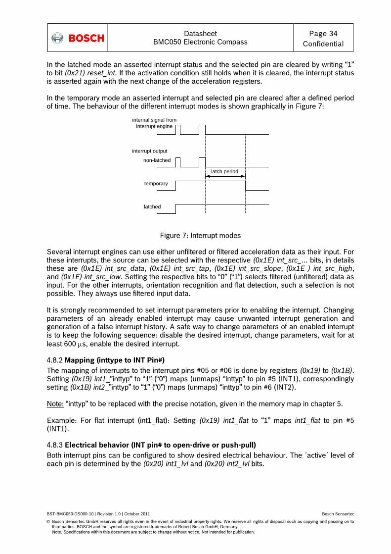
Datasheet
BMC050 Electronic Compass Page 34
Confidential
BST-BMC050-DS000-10 | Revision 1.0 | October 2011 Bosch Sensortec
© Bosch Sensortec GmbH reserves all rights even in the event of industrial property rights. We reserve all rights of disposal such as copying and passing on to
third parties. BOSCH and the symbol are registered trademarks of Robert Bosch GmbH, Germany.
Note: Specifications within this document are subject to change without notice. Not intended for publication.
In the latched mode an asserted interrupt status and the selected pin are cleared by writing “1” to bit (0x21) reset_int. If the activation condition still holds when it is cleared, the interrupt status is asserted again with the next change of the acceleration registers. In the temporary mode an asserted interrupt and selected pin are cleared after a defined period of time. The behaviour of the different interrupt modes is shown graphically in Figure 7:
Figure 7: Interrupt modes
Several interrupt engines can use either unfiltered or filtered acceleration data as their input. For these interrupts, the source can be selected with the respective (0x1E) int_src_... bits, in details these are (0x1E) int_src_data, (0x1E) int_src_tap, (0x1E) int_src_slope, (0x1E ) int_src_high, and (0x1E) int_src_low. Setting the respective bits to “0” (“1”) selects filtered (unfiltered) data as input. For the other interrupts, orientation recognition and flat detection, such a selection is not possible. They always use filtered input data. It is strongly recommended to set interrupt parameters prior to enabling the interrupt. Changing parameters of an already enabled interrupt may cause unwanted interrupt generation and generation of a false interrupt history. A safe way to change parameters of an enabled interrupt is to keep the following sequence: disable the desired interrupt, change parameters, wait for at
least 600 s, enable the desired interrupt.
4.8.2 Mapping (inttype to INT Pin#)
The mapping of interrupts to the interrupt pins #05 or #06 is done by registers (0x19) to (0x1B). Setting (0x19) int1_”inttyp” to “1” (“0”) maps (unmaps) “inttyp” to pin #5 (INT1), correspondingly setting (0x1B) int2_”inttyp” to “1” (“0”) maps (unmaps) “inttyp” to pin #6 (INT2). Note: “inttyp” to be replaced with the precise notation, given in the memory map in chapter 5. Example: For flat interrupt (int1_flat): Setting (0x19) int1_flat to “1” maps int1_flat to pin #5 (INT1).
4.8.3 Electrical behavior (INT pin# to open-drive or push-pull)
Both interrupt pins can be configured to show desired electrical behaviour. The ´active´ level of each pin is determined by the (0x20) int1_lvl and (0x20) int2_lvl bits.
internal signal from
interrupt engine
interrupt output
non-latched
temporary
latched
latch period

Datasheet
BMC050 Electronic Compass Page 35
Confidential
BST-BMC050-DS000-10 | Revision 1.0 | October 2011 Bosch Sensortec
© Bosch Sensortec GmbH reserves all rights even in the event of industrial property rights. We reserve all rights of disposal such as copying and passing on to
third parties. BOSCH and the symbol are registered trademarks of Robert Bosch GmbH, Germany.
Note: Specifications within this document are subject to change without notice. Not intended for publication.
If (0x20) int1_lvl = “1” (“0”) / (0x20) int2_lvl = “1” (“0”), then pin #05 (INT1) / pin #06 (INT2) is active “1” (“0”). In addition to that, also the electric type of the interrupt pins can be selected. By setting bits (0x20) int1_od / (0x20) int2_od to “0”, the interrupt pin output type becomes open-drive, by setting the configuration bits to “1”, the output type becomes push-pull. Remark: The states of both INT pins are not defined during the first 2 ms after power-up.
4.8.4 New data interrupt
This interrupt serves for synchronous reading of acceleration data. It is generated after storing a new value of z-axis acceleration data in the data register. The interrupt is cleared automatically when the next cycle of data acquisition starts. The interrupt status is “0” for at least 50µs. The interrupt mode of the new data interrupt is fixed to non-latched. It is enabled (disabled) by writing “1” (“0”) to bit (0x17) data_en. The interrupt status is stored in bit (0x0A) data_int.
4.8.5 Any-motion (slope) detection
Any-motion detection uses the slope between successive acceleration signals to detect changes in motion. An interrupt is generated when the slope (absolute value of acceleration difference) exceeds a preset threshold. It is cleared as soon as the slope falls below the threshold. The principle is clarified in Figure 8.
Figure 8: Principle of any-motion detection
slope_th
INT
slope
acceleration
acc(t0)
acc(t0−1/(2*bw))
slope(t0)=acc(t0)−acc(t0−1/(2*bw))
time
time
time
slope_dur
slope_dur
Datasheet
BMC050 Electronic Compass Page 36
Confidential
BST-BMC050-DS000-10 | Revision 1.0 | October 2011 Bosch Sensortec
© Bosch Sensortec GmbH reserves all rights even in the event of industrial property rights. We reserve all rights of disposal such as copying and passing on to
third parties. BOSCH and the symbol are registered trademarks of Robert Bosch GmbH, Germany.
Note: Specifications within this document are subject to change without notice. Not intended for publication.
The threshold is set with the value of register (0x28) slope_th. 1 LSB of (0x28) slope_th corresponds to 1 LSB of acceleration data. Therefore, an increment of (0x28) slope_th is 3.91 mg in 2g-range (7.81 mg in 4g-range, 15.6 mg in 8g-range and 31.3 mg in 16g-range). And the maximum value is 996 mg in 2g-range (1.99g in 4g-range, 3.98g in 8g-range and 7.97g in 16g-range). The time difference between the successive acceleration signals depends on the selected bandwidth and equates to 1/(2*bandwidth) (Δt=1/(2*bw)). In order to suppress failure signals, the interrupt is only generated (cleared) if a certain number N of consecutive slope data points is larger (smaller) than the slope threshold given by (0x28) slope_th. This number is set by the (0x27) slope_dur bits. It is N = (0x27) slope_dur + 1 for (0x27). Example: (0x27) slope_dur = 00b, …, 11b = 1decimal, …, 4decimal
4.8.5.1 Enabling (disabling) for each axis
Any-motion detection can be enabled (disabled) for each axis separately by writing “1” (“0”) to bits (0x16) slope_en_x, (0x16) slope_en_y, (0x16) slope_en_z. The criteria for any-motion detection are fulfilled and the slope interrupt is generated if the slope of any of the enabled axes exceeds the threshold (0x28) slope_th for [(0x27) slope_dur +1] consecutive times. As soon as the slopes of all enabled axes fall or stay below this threshold for [(0x27) slope_dur +1] consecutive times the interrupt is cleared unless interrupt signal is latched.
4.8.5.2 Axis and sign information of any motion interrupt
The interrupt status is stored in bit (0x09) slope_int. The any-motion interrupt supplies additional information about the detected slope. The axis which triggered the interrupt is given by that one of bits (0x0B) slope_first_x, (0x0B) slope_first_y, (0x0B) slope_first_z that contains a “1”. The sign of the triggering slope is held in bit (0x0B) slope_sign. If (0x0B) slope_sign = “0” (“1”), the sign is positive (negative).
4.8.5.3 Serial interface and dedicated wake-up mode
When serial interface is active, any-motion detection logic is enabled if any of the axis specific (0x16) slope_en_... register bits are set. To disable the any-motion interrupt, clear all the axis specific (0x16) slope_en_... bits.
4.8.6 Tap sensing
Tap sensing has a functional similarity with a common laptop touch-pad or clicking keys of a computer mouse. A tap event is detected if a pre-defined slope of the acceleration of at least one axis is exceeded. Two different tap events are distinguished: A „single tap‟ is a single event within a certain time, followed by a certain quiet time. A „double tap‟ consists of a first such event followed by a second event within a defined time frame. Only one of the tap interrupts can be enabled at the same time. Single tap interrupt is enabled (disabled) by writing “1” (“0”) to bit (0x16) s_tap_en. Double tap interrupt is enabled (disabled) by writing “1” (“0”) to bit (0x16) d_tap_en. If one tries to enable both interrupts by writing “1” to (0x16) s_tap_en and (0x16) d_tap_en, then only (0x16) d_tap_en keeps the value “1” and the double tap interrupt is enabled. The status of the single tap interrupt is stored in bit (0x09) s_tap_int, the status of the double tap interrupt is stored in bit (0x09) d_tap_int.

Datasheet
BMC050 Electronic Compass Page 37
Confidential
BST-BMC050-DS000-10 | Revision 1.0 | October 2011 Bosch Sensortec
© Bosch Sensortec GmbH reserves all rights even in the event of industrial property rights. We reserve all rights of disposal such as copying and passing on to
third parties. BOSCH and the symbol are registered trademarks of Robert Bosch GmbH, Germany.
Note: Specifications within this document are subject to change without notice. Not intended for publication.
The slope threshold for detecting a tap event is set by bits (0x2B) tap_th. The meaning of (0x2B) tap_th depends on the range setting. 1 LSB of (0x2B) tap_th corresponds to a slope of 62.5mg in 2g-range, 125mg in 4g-range, 250mg in 8g-range, and 500mg in 16g-range. In Figure 9 the meaning of the different timing parameters is visualized:
Figure 9: Timing of tap detection
The parameters (0x2A) tap_shock and (0x2A) tap_quiet apply to both single tap and double tap detection, while (0x2A) tap_dur applies to double tap detection only. Within the duration of (0x2A) tap_shock any slope exceeding (0x2B) tap_th after the first event is ignored. Contrary to this, within the duration of (0x2A) tap_quiet no slope exceeding (0x2B) tap_th must occur, otherwise the first event will be cancelled.
4.8.6.1 Single tap detection
A single tap is detected and the single tap interrupt is generated after the combined durations of (0x2A) tap_shock and (0x2A) tap_quiet, if the corresponding slope conditions are fulfilled. The interrupt is cleared after a delay of 12.5 ms.
tap_shock tap_quiet tap_dur
tap_shock tap_quiet
time
12.5 ms
single tap detection
double tap detection
slope
time
12.5 ms
time
1st tap 2nd tap
tap_th
a

Datasheet
BMC050 Electronic Compass Page 38
Confidential
BST-BMC050-DS000-10 | Revision 1.0 | October 2011 Bosch Sensortec
© Bosch Sensortec GmbH reserves all rights even in the event of industrial property rights. We reserve all rights of disposal such as copying and passing on to
third parties. BOSCH and the symbol are registered trademarks of Robert Bosch GmbH, Germany.
Note: Specifications within this document are subject to change without notice. Not intended for publication.
4.8.6.2 Double tap detection
A double tap is detected and the double tap interrupt is generated if an event fulfilling the conditions for a single tap occurs within the set duration in (0x2A) tap_dur after the completion of the first tap event. The interrupt is cleared after a delay of 12.5 ms.
4.8.6.3 Selecting the timing of tap detection
For each of parameters (0x2A) tap_shock and (0x2A) tap_quiet two values are selectable. By writing “0” (“1”) to bit (0x2A) tap_shock the duration of (0x2A) tap_shock is set to 50 ms (75 ms). By writing “0” (“1”) to bit (0x2A) tap_quiet the duration of (0x2A) tap_quiet is set to 30 ms (20 ms). The length of (0x2A) tap_dur can be selected by setting the (0x2A) tap_dur bits according to Table 17:
Table 17: Selection of tap_dur
(0x2A) tap_dur
length of tap_dur
000b 50 ms
001b 100 ms
010b 150 ms
011b 200 ms
100b 250 ms
101b 375 ms
110b 500 ms
111b 700 ms
4.8.6.4 Axis and sign information of tap sensing
The sign of the slope of the first tap which triggered the interrupt is stored in bit (0x0B) tap_sign (“0” means positive sign, “1” means negative sign). The value of this bit persists after clearing the interrupt. The axis which triggered the interrupt is indicated by bits (0x0B) tap_first_x, (0x0B) tap_first_y, and (0x0B) tap_first_z. The bit corresponding to the triggering axis contains a “1” while the other bits hold a “0”. These bits are cleared together with clearing the interrupt status.
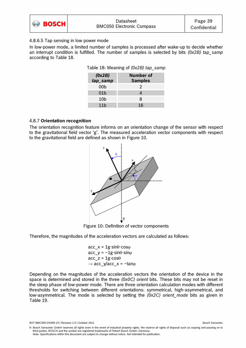
Datasheet
BMC050 Electronic Compass Page 39
Confidential
BST-BMC050-DS000-10 | Revision 1.0 | October 2011 Bosch Sensortec
© Bosch Sensortec GmbH reserves all rights even in the event of industrial property rights. We reserve all rights of disposal such as copying and passing on to
third parties. BOSCH and the symbol are registered trademarks of Robert Bosch GmbH, Germany.
Note: Specifications within this document are subject to change without notice. Not intended for publication.
4.8.6.5 Tap sensing in low power mode
In low-power mode, a limited number of samples is processed after wake-up to decide whether an interrupt condition is fulfilled. The number of samples is selected by bits (0x2B) tap_samp according to Table 18.
Table 18: Meaning of (0x2B) tap_samp
(0x2B) tap_samp
Number of Samples
00b 2
01b 4
10b 8
11b 16
4.8.7 Orientation recognition
The orientation recognition feature informs on an orientation change of the sensor with respect to the gravitational field vector „g‟. The measured acceleration vector components with respect to the gravitational field are defined as shown in Figure 10.
Figure 10: Definition of vector components
Therefore, the magnitudes of the acceleration vectors are calculated as follows:
acc_x = 1g∙sin∙cos
acc_y = −1g∙sin∙sin
acc_z = 1g∙cos
→ acc_y/acc_x = −tan Depending on the magnitudes of the acceleration vectors the orientation of the device in the space is determined and stored in the three (0x0C) orient bits. These bits may not be reset in the sleep phase of low-power mode. There are three orientation calculation modes with different thresholds for switching between different orientations: symmetrical, high-asymmetrical, and low-asymmetrical. The mode is selected by setting the (0x2C) orient_mode bits as given in Table 19.

Datasheet
BMC050 Electronic Compass Page 40
Confidential
BST-BMC050-DS000-10 | Revision 1.0 | October 2011 Bosch Sensortec
© Bosch Sensortec GmbH reserves all rights even in the event of industrial property rights. We reserve all rights of disposal such as copying and passing on to
third parties. BOSCH and the symbol are registered trademarks of Robert Bosch GmbH, Germany.
Note: Specifications within this document are subject to change without notice. Not intended for publication.
Table 19: Orientation mode settings
(0x2C) orient_mode
Orientation Mode
00b symmetrical
01b high-asymmetrical
10b low-asymmetrical
11b symmetrical For each orientation mode the (0x0C) orient bits have a different meaning as shown in Table 20 to Table 22:
Table 20: Meaning of the (0x0C) orient bits in symmetrical mode
(0x0C) orient
Name Angle Condition
x00 portrait upright 315° < < 45° |acc_y| < |acc_x| - „hyst‟ and acc_x - „hyst‟’ ≥ 0
x01 portrait upside down 135° < < 225° |acc_y| < |acc_x| - „hyst‟ and acc_x + „hyst‟ < 0
x10 landscape left 45° < < 135° |acc_y| ≥ |acc_x| + „hyst‟
and acc_y < 0
x11 landscape right 225° < < 315° |acc_y| ≥ |acc_x| + „hyst‟
and acc_y ≥ 0
Table 21: Meaning of the (0x0C) orient bits in high-asymmetrical mode
(0x0C) orient
Name Angle Condition
x00 portrait upright 297° < < 63° |acc_y| < 2·|acc_x| - „hyst‟
and acc_x - „hyst‟ ≥ 0
x01 portrait upside down 117° < < 243° |acc_y| < 2·|acc_x| - „hyst‟
and acc_x + „hyst‟ < 0
x10 landscape left 63° < < 117° |acc_y| ≥ 2·|acc_x| + „hyst‟
and acc_y < 0
x11 landscape right 243° < < 297° |acc_y| ≥ 2·|acc_x| + „hyst‟
and acc_y ≥ 0
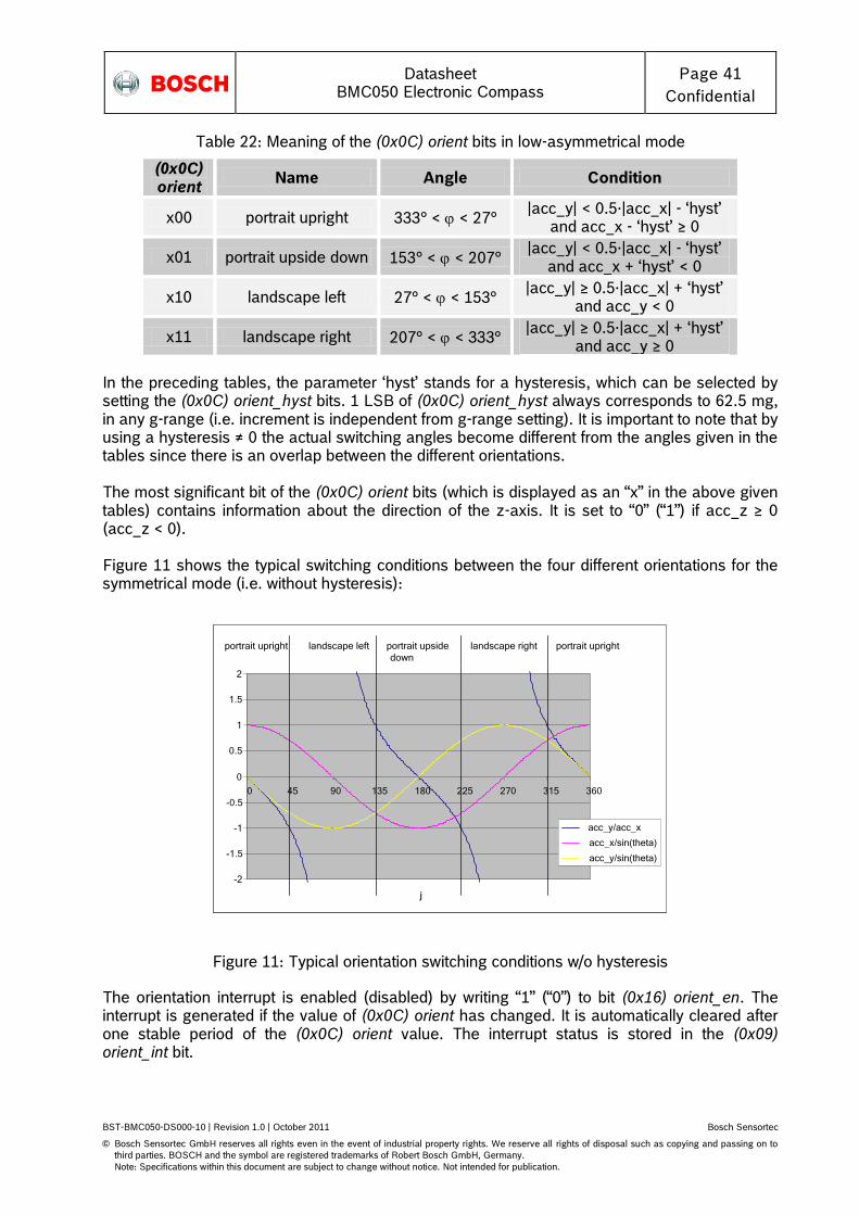
Datasheet
BMC050 Electronic Compass Page 41
Confidential
BST-BMC050-DS000-10 | Revision 1.0 | October 2011 Bosch Sensortec
© Bosch Sensortec GmbH reserves all rights even in the event of industrial property rights. We reserve all rights of disposal such as copying and passing on to
third parties. BOSCH and the symbol are registered trademarks of Robert Bosch GmbH, Germany.
Note: Specifications within this document are subject to change without notice. Not intended for publication.
Table 22: Meaning of the (0x0C) orient bits in low-asymmetrical mode
(0x0C) orient
Name Angle Condition
x00 portrait upright 333° < < 27° |acc_y| < 0.5·|acc_x| - „hyst‟
and acc_x - „hyst‟ ≥ 0
x01 portrait upside down 153° < < 207° |acc_y| < 0.5·|acc_x| - „hyst‟
and acc_x + „hyst‟ < 0
x10 landscape left 27° < < 153° |acc_y| ≥ 0.5·|acc_x| + „hyst‟
and acc_y < 0
x11 landscape right 207° < < 333° |acc_y| ≥ 0.5·|acc_x| + „hyst‟
and acc_y ≥ 0 In the preceding tables, the parameter „hyst‟ stands for a hysteresis, which can be selected by setting the (0x0C) orient_hyst bits. 1 LSB of (0x0C) orient_hyst always corresponds to 62.5 mg, in any g-range (i.e. increment is independent from g-range setting). It is important to note that by using a hysteresis ≠ 0 the actual switching angles become different from the angles given in the tables since there is an overlap between the different orientations. The most significant bit of the (0x0C) orient bits (which is displayed as an “x” in the above given tables) contains information about the direction of the z-axis. It is set to “0” (“1”) if acc_z ≥ 0 (acc_z < 0). Figure 11 shows the typical switching conditions between the four different orientations for the symmetrical mode (i.e. without hysteresis):
-2
-1.5
-1
-0.5
0
0.5
1
1.5
2
0 45 90 135 180 225 270 315 360
phi
acc_y/acc_x
acc_x/sin(theta)
acc_y/sin(theta)
portrait upright landscape left portrait upside
down
landscape right portrait upright
-2
-1.5
-1
-0.5
0
0.5
1
1.5
2
0 45 90 135 180 225 270 315 360
j
acc_y/acc_x
acc_x/sin(theta)
acc_y/sin(theta)
portrait upright landscape left portrait upside
down
landscape right portrait upright
Figure 11: Typical orientation switching conditions w/o hysteresis
The orientation interrupt is enabled (disabled) by writing “1” (“0”) to bit (0x16) orient_en. The interrupt is generated if the value of (0x0C) orient has changed. It is automatically cleared after one stable period of the (0x0C) orient value. The interrupt status is stored in the (0x09) orient_int bit.

Datasheet
BMC050 Electronic Compass Page 42
Confidential
BST-BMC050-DS000-10 | Revision 1.0 | October 2011 Bosch Sensortec
© Bosch Sensortec GmbH reserves all rights even in the event of industrial property rights. We reserve all rights of disposal such as copying and passing on to
third parties. BOSCH and the symbol are registered trademarks of Robert Bosch GmbH, Germany.
Note: Specifications within this document are subject to change without notice. Not intended for publication.
If temporary or latched interrupt mode is used, after the generation of the interrupt the changed (0x0C) orient value is kept fixed as long as the interrupt persists (e. g. until the latch time expires or the interrupt is reset). After clearing the interrupt, the (0x0C) orient is only updated with the next following value change (i.e. with the next occurring interrupt). In order to ensure the continuous availability of up-to-date orientation data it is therefore optimal to use the non-latched interrupt. It is strongly advised against using latched interrupt mode or temporary interrupt mode with latch times above 50 ms for orient recognition.
4.8.7.1 Orientation blocking
The change of the (0x0C) orient value and – as a consequence – the generation of the interrupt can be blocked according to conditions selected by setting the value of the (0x2C) orient_blocking bits as described by Table 23.
Table 23: Blocking conditions for orientation recognition
(0x2C) orient_blocking
Conditions
00b no blocking
01b theta blocking
10b theta blocking
or acceleration slope in any axis > 0.2 g
11b
value of orient is not stable for at least 100 ms or
theta blocking or
acceleration slope in any axis > 0.4 g The theta blocking is defined by the following inequality:
.8
_tan
thetablocking
The parameter blocking_theta of the above given equation stands for the contents of the (0x2D) orient_theta bits. Hereby it is possible to define a blocking angle between 0° and 44.8°. The internal blocking algorithm saturates the acceleration values before further processing. As a consequence, the blocking angles are strictly valid only for a device at rest; they can be different if the device is moved. Example: To get a maximum blocking angle of 19° the parameter blocking_theta is determined in the following way: (8 * tan(19°) )² = 7.588, therefore, blocking_value = 8dec = 001000b has to be chosen. In order to avoid unwanted generation of the orientation interrupt in a nearly flat position (z ~ 0, sign change due to small movements or noise), a hysteresis of 0.2 g is implemented for the z-axis, i. e. a after a sign change the interrupt is only generated after |z| > 0.2 g.

Datasheet
BMC050 Electronic Compass Page 43
Confidential
BST-BMC050-DS000-10 | Revision 1.0 | October 2011 Bosch Sensortec
© Bosch Sensortec GmbH reserves all rights even in the event of industrial property rights. We reserve all rights of disposal such as copying and passing on to
third parties. BOSCH and the symbol are registered trademarks of Robert Bosch GmbH, Germany.
Note: Specifications within this document are subject to change without notice. Not intended for publication.
4.8.8 Flat detection
The flat detection feature gives information about the orientation of the devices´ z-axis relative to the g-vector, i. e. it recognizes whether the device is in a flat position or not. The condition for the device to be in the flat position is
.8
_tan
thetaparameter
Like blocking_theta, used with orientation recognition, the parameter_theta stands for a user-defined setting. In this case the content of the (0x2E) flat_theta bits. The possible flat angles also range from 0° to 44.8°. To ensure proper operation, parameter_theta has to be less than or equal to blocking_theta. The flat interrupt is enabled (disabled) by writing “1” (“0”) to bit (0x16) flat_en. The flat interrupt is generated if the flat value has changed and the new value is stable for at least the time given by the (0x2F) flat_hold_time bits. The flat value is stored in the (0x0C) flat bit if the interrupt is enabled. This value is “1” if the device is in the flat position, it is “0” otherwise. The content of the (0x0C) flat bit is changed only if the interrupt is generated. The interrupt is automatically cleared after one sample period. Its status is stored in the (0x09) flat_int bit. If temporary or latched interrupt mode is used, after the generation of the interrupt the changed (0x0C) flat value is kept fixed as long as the interrupt persists (e. g. until the latch time expires or the interrupt is reset). After clearing the interrupt, the (0x0C) flat value is only updated with the next following value change (i.e. with the next occurring interrupt). The meaning of the (0x2F) flat_hold_time bits can be seen from Table 24.
Table 24: Meaning of flat_hold_time
(0x2F) flat_hold_time
Time
00b 0
01b 512 ms
10b 1024 ms
11b 2048 ms
4.8.9 Low-g interrupt
This interrupt is based on the comparison of acceleration data against a low-g threshold, which is most useful for free-fall detection. The interrupt is enabled (disabled) by writing “1” (“0”) to the (0x17) low_en bit. There are two modes available, „single‟ mode and „sum‟ mode. In „single‟ mode, the acceleration of each axis is compared with the threshold; in „sum‟ mode, the sum of absolute values of all accelerations |acc_x| + |acc_y| + |acc_z| is compared with the threshold. The mode is selected by the contents of the (0x24) low_mode bit: “0” means „single‟ mode, “1” means „sum‟ mode. The low-g threshold is set through the (0x23) low_th register. 1 LSB of (0x23) low_th always corresponds to an acceleration of 7.81 mg (i.e. increment is independent from g-range setting).

Datasheet
BMC050 Electronic Compass Page 44
Confidential
BST-BMC050-DS000-10 | Revision 1.0 | October 2011 Bosch Sensortec
© Bosch Sensortec GmbH reserves all rights even in the event of industrial property rights. We reserve all rights of disposal such as copying and passing on to
third parties. BOSCH and the symbol are registered trademarks of Robert Bosch GmbH, Germany.
Note: Specifications within this document are subject to change without notice. Not intended for publication.
A hysteresis can be selected by setting the (0x24) low_hy bits. 1 LSB of (0x24) low_hy always corresponds to an acceleration difference of 125 mg in any g-range (as well, increment is independent from g-range setting). The low-g interrupt is generated if the absolute values of the acceleration of all axes (´and´ relation, in case of single mode) or their sum (in case of sum mode) are lower than the threshold for at least the time defined by the (0x22) low_dur register. The interrupt is reset if the absolute value of the acceleration of at least one axis (´or´ relation, in case of single mode) or the sum of absolute values (in case of sum mode) is higher than the threshold plus the hysteresis for at least one data acquisition. In bit (0x09) low_int the interrupt status is stored. The relation between the content of (0x22) low_dur and the actual delay of the interrupt generation is: delay [ms] = [(0x22) low_dur + 1] • 2 ms. Therefore, possible delay times range from 2 ms to 512 ms.
4.8.10 High-g interrupt
This interrupt is based on the comparison of acceleration data against a high-g threshold for the detection of shock or other high-acceleration events. The high-g interrupt is enabled (disabled) per axis by writing “1” (“0”) to bits (0x17) high_en_x, (0x17) high_en_y, and (0x17) high_en_z, respectively. The high-g threshold is set through the (0x26) high_th register. The meaning of an LSB of (0x26) high_th depends on the selected g-range: it corresponds to 7.81 mg in 2g-range, 15.63 mg in 4g-range, 31.25 mg in 8g-range, and 62.5 mg in 16g-range (i.e. increment depends from g-range setting). A hysteresis can be selected by setting the (0x24) high_hy bits. Analogously to (0x26) high_th, the meaning of an LSB of (0x24) high_hy is g-range dependent: it corresponds to an acceleration difference of 125 mg in 2g-range, 250 mg in 4g-range, 500 mg in 8g-range, and 1000mg in 16g-range (as well, increment depends from g-range setting). The high-g interrupt is generated if the absolute value of the acceleration of at least one of the enabled axes (´or´ relation) is higher than the threshold for at least the time defined by the (0x25) high_dur register. The interrupt is reset if the absolute value of the acceleration of all enabled axes (´and´ relation) is lower than the threshold minus the hysteresis for at least the time defined by the (0x25) high_dur register. In bit (0x09) high_int the interrupt status is stored. The relation between the content of (0x25) high_dur and the actual delay of the interrupt generation is delay [ms] = [(0x22) low_dur + 1] • 2 ms. Therefore, possible delay times range from 2 ms to 512 ms.
4.8.10.1 Axis and sign information of high-g interrupt
The axis which triggered the interrupt is indicated by bits (0x0C) high_first_x, (0x0C) high_first_y, and (0x0C) high_first_z. The bit corresponding to the triggering axis contains a “1” while the other bits hold a “0”. These bits are cleared together with clearing the interrupt status. The sign of the triggering acceleration is stored in bit (0x0C) high_sign. If (0x0C) high_sign = “0” (“1”), the sign is positive (negative).

Datasheet
BMC050 Electronic Compass Page 45
Confidential
BST-BMC050-DS000-10 | Revision 1.0 | October 2011 Bosch Sensortec
© Bosch Sensortec GmbH reserves all rights even in the event of industrial property rights. We reserve all rights of disposal such as copying and passing on to
third parties. BOSCH and the symbol are registered trademarks of Robert Bosch GmbH, Germany.
Note: Specifications within this document are subject to change without notice. Not intended for publication.
4.9 Magnetometer interrupt controller
Four magnetometer based interrupt engines are integrated in the magnetometer part of BMC050: Low-Threshold, High-Threshold, Overflow and Data Ready (DRDY). Each interrupt can be enabled independently. When enabled, an interrupt sets the corresponding status bit in the interrupt status register (0x4A) when its condition is satisfied. When the “Interrupt Pin Enable” bit (register 0x4E bit6) is set, any occurring activated interrupts are flagged on the BMC050‟s INT3 output pin. By default, the interrupt pin is disabled (high-Z status). Low-Threshold, High-Threshold and Overflow interrupts are mapped to the INT3 pin when enabled, Data Ready (DRDY) interrupt is mapped to the DRDY pin of BMC050 when enabled. For High- and Low-Threshold interrupts each axis X/Y/Z can be enabled separately for interrupt detection in the registers “High Int Z en”, “High Int Y en”, “High Int X en”, “Low Int Z en”, “Low Int Y En” and “Low Int X En” in register 0x4D bit5-bit0. Overflow interrupt is shared for X, Y and Z axis. When the “Data Ready Pin En” bit (register 0x4E bit7) is set, the Data Ready (DRDY) interrupt event is flagged on the BMC050‟s DRDY output pin (by default the “Data Ready Pin En” bit is not set and DRDY pin is in high-Z state). The interrupt status registers are updated together with writing new data into the magnetic field data registers. The status bits for Low-/High-Threshold interrupts are located in register 0x4A, the Data Ready (DRDY) status flag is located at register 0x48 bit0. If an interrupt is disabled, all active status bits and pins are reset after the next measurement was performed.
4.9.1 General features
An interrupt is cleared depending on the selected interrupt mode, which is common to all interrupts. There are two different interrupt modes: non-latched and latched. All interrupts (except Data Ready) can be latched or non-latched. Data Ready (DRDY) is always cleared after readout of data registers ends. A non-latched interrupt will be cleared on a new measurement when the interrupt condition is not valid anymore, whereas a latched interrupt will stay high until the interrupts status register (0x4A) is read out. After reading the interrupt status, both the interrupt status bits and the interrupt pin are reset. The mode is selected by the “Interrupt latch” bit (register 0x4A bit1), where the default setting of “1” means latched. Figure 12 shows the difference between the modes for the example Low-Threshold interrupt. INT3 and DRDY pin polarity can be changed by the “Interrupt polarity” bit (register 0x4E bit0) and “DR polarity” (register 0x4E bit2), from the default high active (“1”) to low active (“0”).
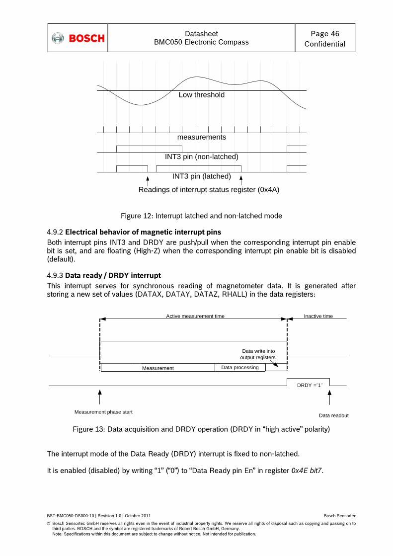
Datasheet
BMC050 Electronic Compass Page 46
Confidential
BST-BMC050-DS000-10 | Revision 1.0 | October 2011 Bosch Sensortec
© Bosch Sensortec GmbH reserves all rights even in the event of industrial property rights. We reserve all rights of disposal such as copying and passing on to
third parties. BOSCH and the symbol are registered trademarks of Robert Bosch GmbH, Germany.
Note: Specifications within this document are subject to change without notice. Not intended for publication.
Figure 12: Interrupt latched and non-latched mode
4.9.2 Electrical behavior of magnetic interrupt pins
Both interrupt pins INT3 and DRDY are push/pull when the corresponding interrupt pin enable bit is set, and are floating (High-Z) when the corresponding interrupt pin enable bit is disabled (default).
4.9.3 Data ready / DRDY interrupt
This interrupt serves for synchronous reading of magnetometer data. It is generated after storing a new set of values (DATAX, DATAY, DATAZ, RHALL) in the data registers:
Figure 13: Data acquisition and DRDY operation (DRDY in “high active” polarity)
The interrupt mode of the Data Ready (DRDY) interrupt is fixed to non-latched. It is enabled (disabled) by writing “1” (“0”) to “Data Ready pin En” in register 0x4E bit7.
Low threshold
measurements
INT3 pin (non-latched)
INT3 pin (latched)
Readings of interrupt status register (0x4A)
Active measurement time
Preset time Measurement Data processing
Data write into
output registers
DRDY =’1 ’
Measurement phase startData readout
Measurement Data processing
Inactive time
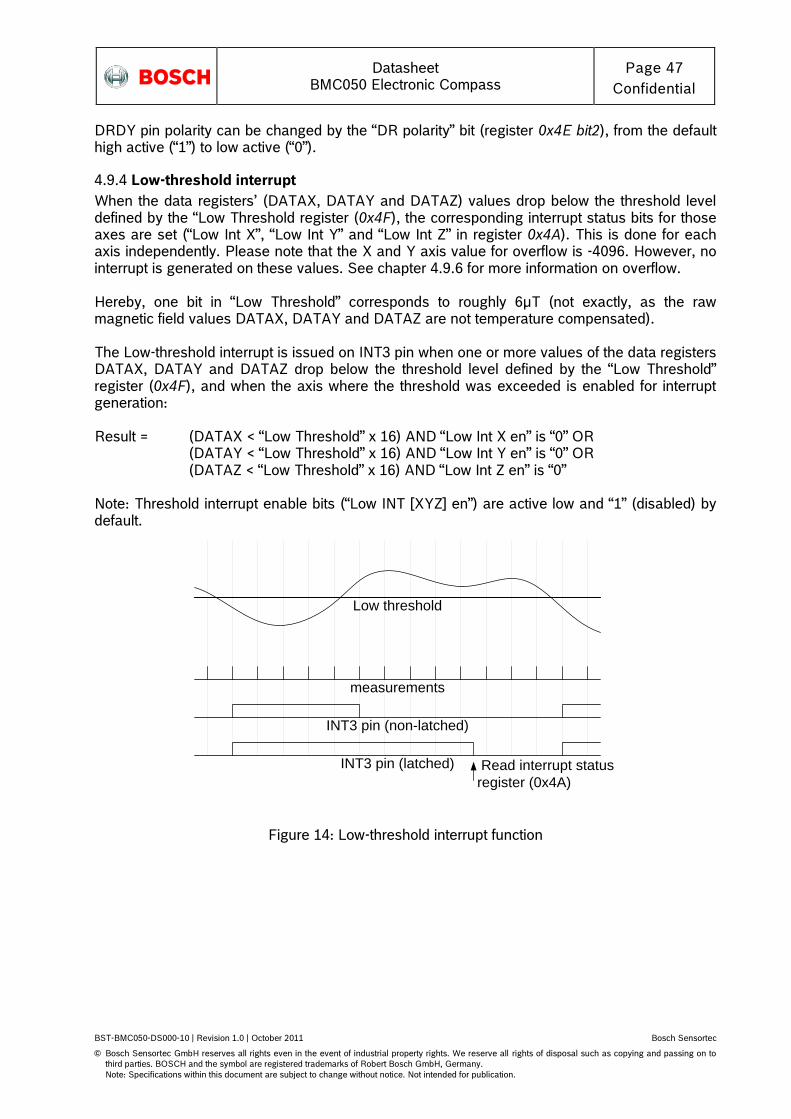
Datasheet
BMC050 Electronic Compass Page 47
Confidential
BST-BMC050-DS000-10 | Revision 1.0 | October 2011 Bosch Sensortec
© Bosch Sensortec GmbH reserves all rights even in the event of industrial property rights. We reserve all rights of disposal such as copying and passing on to
third parties. BOSCH and the symbol are registered trademarks of Robert Bosch GmbH, Germany.
Note: Specifications within this document are subject to change without notice. Not intended for publication.
DRDY pin polarity can be changed by the “DR polarity” bit (register 0x4E bit2), from the default high active (“1”) to low active (“0”).
4.9.4 Low-threshold interrupt
When the data registers‟ (DATAX, DATAY and DATAZ) values drop below the threshold level defined by the “Low Threshold register (0x4F), the corresponding interrupt status bits for those axes are set (“Low Int X”, “Low Int Y” and “Low Int Z” in register 0x4A). This is done for each axis independently. Please note that the X and Y axis value for overflow is -4096. However, no interrupt is generated on these values. See chapter 4.9.6 for more information on overflow. Hereby, one bit in “Low Threshold” corresponds to roughly 6µT (not exactly, as the raw magnetic field values DATAX, DATAY and DATAZ are not temperature compensated). The Low-threshold interrupt is issued on INT3 pin when one or more values of the data registers DATAX, DATAY and DATAZ drop below the threshold level defined by the “Low Threshold” register (0x4F), and when the axis where the threshold was exceeded is enabled for interrupt generation: Result = (DATAX < “Low Threshold” x 16) AND “Low Int X en” is “0” OR
(DATAY < “Low Threshold” x 16) AND “Low Int Y en” is “0” OR (DATAZ < “Low Threshold” x 16) AND “Low Int Z en” is “0”
Note: Threshold interrupt enable bits (“Low INT [XYZ] en”) are active low and “1” (disabled) by default.
Figure 14: Low-threshold interrupt function
a a
Low threshold
measurements
INT3 pin (non-latched)
INT3 pin (latched) Read interrupt status
register (0x4A)
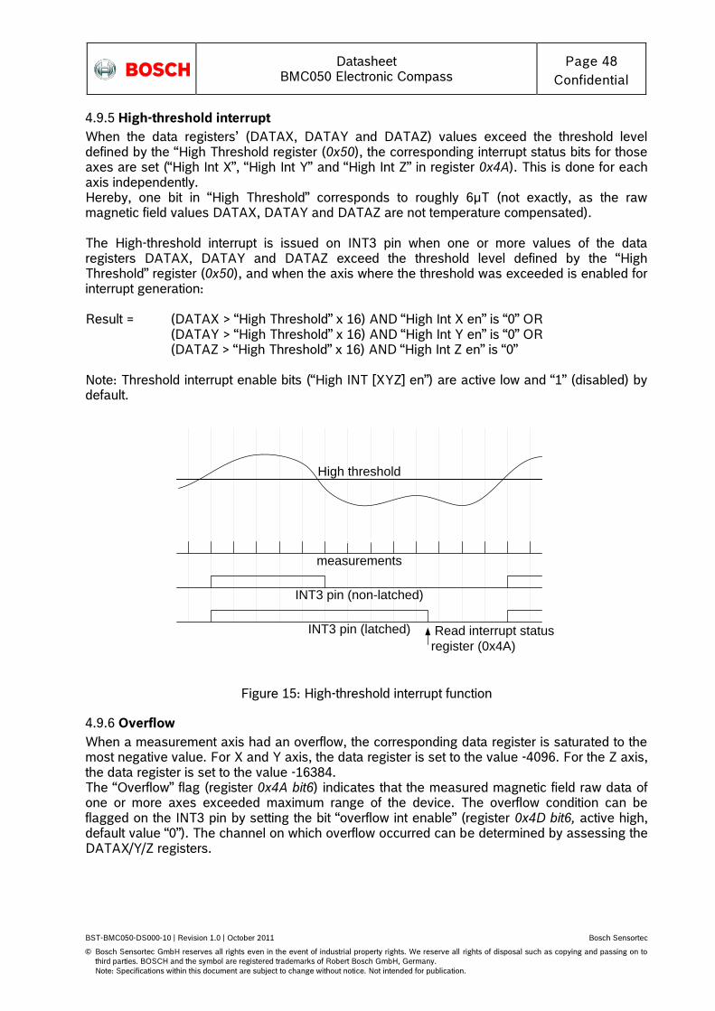
Datasheet
BMC050 Electronic Compass Page 48
Confidential
BST-BMC050-DS000-10 | Revision 1.0 | October 2011 Bosch Sensortec
© Bosch Sensortec GmbH reserves all rights even in the event of industrial property rights. We reserve all rights of disposal such as copying and passing on to
third parties. BOSCH and the symbol are registered trademarks of Robert Bosch GmbH, Germany.
Note: Specifications within this document are subject to change without notice. Not intended for publication.
4.9.5 High-threshold interrupt
When the data registers‟ (DATAX, DATAY and DATAZ) values exceed the threshold level defined by the “High Threshold register (0x50), the corresponding interrupt status bits for those axes are set (“High Int X”, “High Int Y” and “High Int Z” in register 0x4A). This is done for each axis independently. Hereby, one bit in “High Threshold” corresponds to roughly 6µT (not exactly, as the raw magnetic field values DATAX, DATAY and DATAZ are not temperature compensated). The High-threshold interrupt is issued on INT3 pin when one or more values of the data registers DATAX, DATAY and DATAZ exceed the threshold level defined by the “High Threshold” register (0x50), and when the axis where the threshold was exceeded is enabled for interrupt generation: Result = (DATAX > “High Threshold” x 16) AND “High Int X en” is “0” OR
(DATAY > “High Threshold” x 16) AND “High Int Y en” is “0” OR (DATAZ > “High Threshold” x 16) AND “High Int Z en” is “0”
Note: Threshold interrupt enable bits (“High INT [XYZ] en”) are active low and “1” (disabled) by default.
Figure 15: High-threshold interrupt function
4.9.6 Overflow
When a measurement axis had an overflow, the corresponding data register is saturated to the most negative value. For X and Y axis, the data register is set to the value -4096. For the Z axis, the data register is set to the value -16384. The “Overflow” flag (register 0x4A bit6) indicates that the measured magnetic field raw data of one or more axes exceeded maximum range of the device. The overflow condition can be flagged on the INT3 pin by setting the bit “overflow int enable” (register 0x4D bit6, active high, default value “0”). The channel on which overflow occurred can be determined by assessing the DATAX/Y/Z registers.
High threshold
measurements
INT3 pin (non-latched)
INT3 pin (latched) Read interrupt status
register (0x4A)
a a
Datasheet
BMC050 Electronic Compass Page 49
Confidential
BST-BMC050-DS000-10 | Revision 1.0 | October 2011 Bosch Sensortec
© Bosch Sensortec GmbH reserves all rights even in the event of industrial property rights. We reserve all rights of disposal such as copying and passing on to
third parties. BOSCH and the symbol are registered trademarks of Robert Bosch GmbH, Germany.
Note: Specifications within this document are subject to change without notice. Not intended for publication.
5. Accelerometer register description
5.1 General remarks
The entire communication with the device is performed by reading from and writing to registers. Registers have a width of 8 bits; they are mapped to a common space of 64 addresses from (0x00) up to (0x3F). Within the used range there are several registers which are either completely or partially marked as „reserved‟. Any reserved bit is ignored when it is written and no specific value is guaranteed when read. It is recommended not to use registers at all which are completely marked as „reserved‟. Further-more it is recommended to mask out (logical and with zero) reserved bits of registers which are partially marked as reserved. Registers with addresses from (0x00) up to (0x0E) are read-only. Any attempt to write to these registers is ignored. There are bits within some registers that connected with an action to be done and, therefore, are intended for write-only access, e. g. (0x21) reset_int or the entire (0x14) softreset register. Such bits always give “0” when read.

Datasheet
BMC050 Electronic Compass Page 50
Confidential
BST-BMC050-DS000-10 | Revision 1.0 | October 2011 Bosch Sensortec
© Bosch Sensortec GmbH reserves all rights even in the event of industrial property rights. We reserve all rights of disposal such as copying and passing on to
third parties. BOSCH and the symbol are registered trademarks of Robert Bosch GmbH, Germany.
Note: Specifications within this document are subject to change without notice. Not intended for publication.
5.2 Register map
5.3 Chip ID
Register (0x00) Chip ID contains the accelerometer chip identification number.
Table 25: Chip identification number, register (0x00)
Bit 7 Bit 6 Bit 5 Bit 4 Bit 3 Bit 2 Bit 1 Bit 0
0 0 0 0 0 0 1 1
Register (0x01) is reserved
Register Address Default Value bit7 bit6 bit5 bit4 bit3 bit2 bit1 bit0
0x3F 0x00
0x3E 0x00
0x3D 0x00
0x3C 0x00
0x3B 0x00
0x3A 0x00
0x39 0x00
0x38 0x00
0x37 0x00 reserved cut_off
0x36 0x00 offset_reset cal_rdy reserved hp_z_en hp_y_en hp_x_en
0x35 0x00
0x34 0x00 i2c_wdt_en i2c_wdt_sel spi3
0x33 0x04 nvm_load nvm_rdy nvm_prog_trig nvm_prog_mode
0x32 0x70 self_test_sign
0x31 0x00
0x30 0x00
0x2F 0x10
0x2E 0x08
0x2D 0x08
0x2C 0x18 reserved
0x2B 0x0A reserved
0x2A 0x04 tap_quiet tap_shock
0x29 0x00
0x28 0x14
0x27 0x00
0x26 0xC0
0x25 0x0F
0x24 0x81 low_mode
0x23 0x30
0x22 0x09
0x21 0x00 reset_int
0x20 0x05 int2_od int2_lvl int1_od int1_lvl
0x1F 0x00
0x1E 0x00 int_src_data int_src_tap reserved int_src_slope int_src_high int_src_low
0x1D 0x00
0x1C 0x00
0x1B 0x00 int2_flat int2_orient int2_s_tap int2_d_tap reserved int2_slope int2_high int2_low
0x1A 0x00 int2_data int1_data
0x19 0x00 int1_flat int1_orient int1_s_tap int1_d_tap reserved int1_slope int1_high int1_low
0x18 0x00
0x17 0x00 data_en low_en high_en_z high_en_y high_en_x
0x16 0x00 flat_en orient_en s_tap_en d_tap_en reserved slope_en_z slope_en_y slope_en_x
0x15 0x00
0x14 0x00
0x13 0x00 data_high_bw shadow_dis
0x12 0x00
0x11 0x00 suspend lowpower_en reserved reserved
0x10 0x1F
0x0F 0x03
0x0E 0x00
0x0D 0x00
0x0C 0x00 flat high_sign high_first_z high_first_y high_first_x
0x0B 0x00 tap_sign tap_first_z tap_first_y tap_first_x slope_sign slope_first_z slope_first_y slope_first_x
0x0A 0x00 data_int reserved
0x09 0x00 flat_int orient_int s_tap_int d_tap_int reserved slope_int high_int low_int
0x08 0x00
0x07 0x00
0x06 0x00 new_data_z
0x05 0x00
0x04 0x00 new_data_y
0x03 0x00
0x02 0x00 new_data_x
0x01 0x21
0x00 0x03
w/r
write only
read only
reserved
reserved
acc_z_lsb<1:0> 0
acc_x_lsb<1:0> 0
acc_y_lsb<1:0> 0
acc_x_msb<9:2>
acc_y_msb<9:2>
orient[2:0]
reserved
reserved
reserved
reserved
reserved
reserved
reserved
reserved
sleep_dur<3:0>
bw<4:0>
low_th<7:0>
softreset
reserved
reserved
reserved
reserved
reserved
low_dur<7:0>
reserved
reserved
reserved
reserved
reserved
cal_trigger<1:0>
offset_filt_x<7:0>
offset_target_z<1:0>
offset_filt_y<7:0>
offset_filt_z<7:0>
offset_target_y<1:0> offset_target_x<1:0>
offset_unfilt_z<7:0>
offset_unfilt_y<7:0>
orient_theta<5:0>
reserved
offset_unfilt_x<7:0>
reserved
reserved
reserved
reserved
self_test_axis
acc_z_msb<9:2>
range<3:0>
reserved
tap_th<4:0>
flat_theta<5:0>
flat_hold_time<1:0> reserved
reserved
orient_blocking<1:0> orient_mode<1:0>
reserved
tap_samp<1:0>
reserved
high_th<7:0>
reserved
tap_dur<2:0>
reserved
orient_hyst<2:0>
Chip ID
high_dur<7:0>
slope_th<7:0>
low_hy<1:0>
slope_dur<1:0>
high_hy<1:0>
temp<7:0>
reserved
latch_int<3:0>
reserved

Datasheet
BMC050 Electronic Compass Page 51
Confidential
BST-BMC050-DS000-10 | Revision 1.0 | October 2011 Bosch Sensortec
© Bosch Sensortec GmbH reserves all rights even in the event of industrial property rights. We reserve all rights of disposal such as copying and passing on to
third parties. BOSCH and the symbol are registered trademarks of Robert Bosch GmbH, Germany.
Note: Specifications within this document are subject to change without notice. Not intended for publication.
5.4 Acceleration data
Register (0x02) contains the LSB part of x-axis acceleration data and the new data flag for the x-axis.
Table 26: LSB part of x-axis acceleration, register (0x02)
(0x02) Bit Name Description
Bit 7 acc_x_lsb <1> Bit 1 of x-axis acceleration data
Bit 6 acc_x_lsb <0> Bit 0 of x-axis acceleration data = x LSB
Bit 5 - (fixed to 0)
Bit 4 - (fixed to 0)
Bit 3 - (fixed to 0)
Bit 2 - (fixed to 0)
Bit 1 - (fixed to 0)
Bit 0 new_data_x New data flag of x-axis
Register (0x03) contains the MSB part of x-axis acceleration data.
Table 27: MSB part of x-axis acceleration, register (0x03)
(0x03) Bit
Name Description
Bit 7 acc_x_msb <9> Bit 9 of x-axis acceleration data = x MSB
Bit 6 acc_x_msb <8> Bit 8 of x-axis acceleration data
Bit 5 acc_x_msb <7> Bit 7 of x-axis acceleration data
Bit 4 acc_x_msb <6> Bit 6 of x-axis acceleration data
Bit 3 acc_x_msb <5> Bit 5 of x-axis acceleration data
Bit 2 acc_x_msb <4> Bit 4 of x-axis acceleration data
Bit 1 acc_x_msb <3> Bit 3 of x-axis acceleration data
Bit 0 acc_x_msb <2> Bit 2 of x-axis acceleration data
Register (0x04) contains the LSB part of y-axis acceleration data and the new data flag for the y-axis.
Table 28: LSB part of y-axis acceleration, register (0x04)
(0x04) Bit
Name Description
Bit 7 acc_y_lsb <1> Bit 1 of y-axis acceleration data
Bit 6 acc_y_lsb <0> Bit 0 of y-axis acceleration data = y LSB
Bit 5 - (fixed to 0)
Bit 4 - (fixed to 0)
Bit 3 - (fixed to 0)
Bit 2 - (fixed to 0)
Bit 1 - (fixed to 0)
Bit 0 new_data_y New data flag of y-axis
Datasheet
BMC050 Electronic Compass Page 52
Confidential
BST-BMC050-DS000-10 | Revision 1.0 | October 2011 Bosch Sensortec
© Bosch Sensortec GmbH reserves all rights even in the event of industrial property rights. We reserve all rights of disposal such as copying and passing on to
third parties. BOSCH and the symbol are registered trademarks of Robert Bosch GmbH, Germany.
Note: Specifications within this document are subject to change without notice. Not intended for publication.
Register (0x05) contains the MSB part of acceleration data for the y-axis.
Table 29: MSB part of y-axis acceleration, register (0x05)
(0x05) Bit
Name Description
Bit 7 acc_y_msb <9> Bit 9 of y-axis acceleration data = y MSB
Bit 6 acc_y_msb <8> Bit 8 of y-axis acceleration data
Bit 5 acc_y_msb <7> Bit 7 of y-axis acceleration data
Bit 4 acc_y_msb <6> Bit 6 of y-axis acceleration data
Bit 3 acc_y_msb <5> Bit 5 of y-axis acceleration data
Bit 2 acc_y_msb <4> Bit 4 of y-axis acceleration data
Bit 1 acc_y_msb <3> Bit 3 of y-axis acceleration data
Bit 0 acc_y_msb <2> Bit 2 of y-axis acceleration data
Register (0x06) contains the LSB part of acceleration data and the new data flag for the z-axis.
Table 30: LSB part of y-axis acceleration, register (0x06)
(0x06) Bit
Name Description
Bit 7 acc_z_lsb <1> Bit 1 of z-axis acceleration data
Bit 6 acc_z_lsb <0> Bit 0 of z-axis acceleration data = z LSB
Bit 5 - (fixed to 0)
Bit 4 - (fixed to 0)
Bit 3 - (fixed to 0)
Bit 2 - (fixed to 0)
Bit 1 - (fixed to 0)
Bit 0 new_data_z New data flag of z-axis
Register (0x07) contains the MSB part of acceleration data for the z-axis.
Table 31: MSB part of z-axis acceleration, register (0x07)
(0x07) Bit
Name Description
Bit 7 acc_z_msb <9> Bit 9 of z-axis acceleration data = z MSB
Bit 6 acc_z_msb <8> Bit 8 of z-axis acceleration data
Bit 5 acc_z_msb <7> Bit 7 of z-axis acceleration data
Bit 4 acc_z_msb <6> Bit 6 of z-axis acceleration data
Bit 3 acc_z_msb <5> Bit 5 of z-axis acceleration data
Bit 2 acc_z_msb <4> Bit 4 of z-axis acceleration data
Bit 1 acc_z_msb <3> Bit 3 of z-axis acceleration data
Bit 0 acc_z_msb <2> Bit 2 of z-axis acceleration data

Datasheet
BMC050 Electronic Compass Page 53
Confidential
BST-BMC050-DS000-10 | Revision 1.0 | October 2011 Bosch Sensortec
© Bosch Sensortec GmbH reserves all rights even in the event of industrial property rights. We reserve all rights of disposal such as copying and passing on to
third parties. BOSCH and the symbol are registered trademarks of Robert Bosch GmbH, Germany.
Note: Specifications within this document are subject to change without notice. Not intended for publication.
5.5 Temperature data
Register (0x08) temp contains temperature data in two‟s complement representation. Center temperature = 24 °C i.e. (0x08) temp = 00000000b 1 LSB increment of temperature sensor is 0.5 °C (0.9 °F).
Table 32: Temperature data, register (0x08)
Bit 7 Bit 6 Bit 5 Bit 4 Bit 3 Bit 2 Bit 1 Bit 0
Temp <7>
Temp <6>
Temp <5>
Temp <4>
Temp <3>
Temp <2>
Temp <1>
Temp <0>
5.6 Status registers
Register (0x09) contains the states of several interrupts.
Table 33: Interrupt status, register (0x09)
(0x09) Bit
Name Description
Bit 7 flat_int Flat interrupt status
Bit 6 orient_int Orientation interrupt status
Bit 5 s_tap_int Single tap interrupt status
Bit 4 d_tap_int Double tap interrupt status
Bit 3 - reserved - reserved
Bit 2 slope_int Slope interrupt status
Bit 1 high_int High-g interrupt status
Bit 0 low_int Low-g interrupt status
Register (0x0A) contains the status of the new data interrupt.
Table 34: New data status, register (0x0A)
(0x0A) Bit Name Description
Bit 7 data_int New data interrupt status
Bit 6 - reserved - reserved
Bit 5 - reserved - reserved
Bit 4 - reserved - reserved
Bit 3 - reserved - reserved
Bit 2 - reserved - reserved
Bit 1 - reserved - reserved
Bit 0 - reserved - reserved

Datasheet
BMC050 Electronic Compass Page 54
Confidential
BST-BMC050-DS000-10 | Revision 1.0 | October 2011 Bosch Sensortec
© Bosch Sensortec GmbH reserves all rights even in the event of industrial property rights. We reserve all rights of disposal such as copying and passing on to
third parties. BOSCH and the symbol are registered trademarks of Robert Bosch GmbH, Germany.
Note: Specifications within this document are subject to change without notice. Not intended for publication.
Register (0x0B) contains the sign and triggering axis information for the tap and slope interrupts. Here tap interrupt comprises both single and double tap interrupt.
Table 35: Tap and slope interrupts status, register (0x0B)
(0x0B) Bit Name Description
Bit 7 tap_sign Sign of 1st tap that triggered the interrupt (“0”=positive, “1”=negative)
Bit 6 tap_first_z “1” indicates that z-axis is triggering axis of tap interrupt
Bit 5 tap_first_y “1” indicates that y-axis is triggering axis of tap interrupt
Bit 4 tap_first_x “1” indicates that x-axis is triggering axis of tap interrupt
Bit 3 slope_sign Sign of slope that triggered the interrupt (“0”=positive, “1”=negative)
Bit 2 slope_first_z “1” indicates that z-axis is triggering axis of slope interrupt
Bit 1 slope_first_y “1” indicates that y-axis is triggering axis of slope interrupt
Bit 0 slope_first_x “1” indicates that x-axis is triggering axis of slope interrupt
Register (0x0C) contains the flat and orientation status, and the sign and triggering axis information for the high-g interrupt. Registers (0x0D) and (0x0E) are reserved.
Table 36: Flat and orientation Status, register (0x0C)
(0x0C) Bit Name Description
Bit 7 flat flat detection (“1” if flat condition is fulfilled, “0” otherwise)
Bit 6 orient <2> orientation value of z-axis (“0“ if upward looking, “1“ if downward looking)
Bit 5 orient <1> orientation value of x-y plane (“00”=portrait upright, “01”=portrait upside-down, “10”=landscape left, “11”=landscape right)
Bit 4 orient <0>
Bit 3 high_sign Sign of slope that triggered the interrupt (“0”=positive, “1”=negative)
Bit 2 high_first_z “1” indicates that z-axis is triggering axis of high-g interrupt
Bit 1 high_first_y “1” indicates that y-axis is triggering axis of high-g interrupt
Bit 0 high_first_x “1” indicates that x-axis is triggering axis of high-g interrupt
Registers (0x0D) and (0x0E) are reserved.
Datasheet
BMC050 Electronic Compass Page 55
Confidential
BST-BMC050-DS000-10 | Revision 1.0 | October 2011 Bosch Sensortec
© Bosch Sensortec GmbH reserves all rights even in the event of industrial property rights. We reserve all rights of disposal such as copying and passing on to
third parties. BOSCH and the symbol are registered trademarks of Robert Bosch GmbH, Germany.
Note: Specifications within this document are subject to change without notice. Not intended for publication.
5.7 g-range selection
Register (0x0F) contains the selection of the g-range. Proper settings for (0x0F) range are “0011b” (selects ±2g range), “0101b” (selects ±4g range), “1000b” (selects ±8g range), “1100b” (selects ±16g range). All other settings are irregular; if such a setting is used, ±2g range is selected. Default value of (0x0F) range (after reset) is “0011b”.
Table 37: g-range, register (0x0F)
Bit 7 Bit 6 Bit 5 Bit 4 Bit 3 Bit 2 Bit 1 Bit 0
reserved
reserved
reserved
reserved
range <3>
range <2>
range <1>
range <0>
5.8 Bandwidths
Register (0x10) contains the selection of the bandwidth for filtered acceleration data. Settings for (0x10) bw are “00xxxb” (bandwidth = 7.81 Hz), “01000b” (bandwidth = 7.81 Hz), “01001b” (bandwidth = 15.63 Hz), “01010b” (bandwidth = 31.25 Hz), “01011b” (bandwidth = 62.5 Hz), “01100b” (bandwidth = 125 Hz), “01101b” (bandwidth = 250 Hz), “01110b” (bandwidth = 500 Hz), “01111b” (bandwidth = 1000 Hz), “1xxxxb” (bandwidth = 1000 Hz). Default value of (0x10) bw (after reset) is “11111b”. It is recommended to actively use the range from “01000b” to “01111b” only in order to be compatible with future products.
Table 38: Bandwidths, register (0x10)
Bit 7 Bit 6 Bit 5 Bit 4 Bit 3 Bit 2 Bit 1 Bit 0
reserved reserved reserved bw <4> bw <3> bw <2> bw <1> bw <0>
5.9 Power modes
Register (0x11) contains the configuration of the power modes. (0x11) suspend = “1” (“0”) sets (resets) suspend mode; default value of (0x11) suspend is “0”. (0x11) lowpower_en = “1” (“0”) sets (resets) low-power mode, default value of (0x11) lowpower_en is “0”. The settings for (0x11) sleep_dur are “0000b” to “0101b” (sleep phase duration = 0.5 ms), “0110b” (sleep phase duration = 1 ms), “0111b” (sleep phase duration = 2 ms), “1000b” (sleep phase duration = 4 ms), “1001b” (sleep phase duration = 6 ms), “1010b” (sleep phase duration = 10 ms), “1011b” (sleep phase duration = 25 ms), “1100b” (sleep phase duration = 50 ms), “1101b” (sleep phase duration = 100 ms), “1110b” (sleep phase duration = 500 ms), “1111b” (sleep phase duration = 1 s). Default value of (0x11) sleep_dur is “0000b”.
Table 39: Power modes, register (0x11)
Bit 7 Bit 6 Bit 5 Bit 4 Bit 3 Bit 2 Bit 1 Bit 0
suspend
lowpower
_en
reserved
sleep_ dur<3>
sleep_ dur<2>
sleep_ dur<1>
sleep_ dur<0>
reserved

Datasheet
BMC050 Electronic Compass Page 56
Confidential
BST-BMC050-DS000-10 | Revision 1.0 | October 2011 Bosch Sensortec
© Bosch Sensortec GmbH reserves all rights even in the event of industrial property rights. We reserve all rights of disposal such as copying and passing on to
third parties. BOSCH and the symbol are registered trademarks of Robert Bosch GmbH, Germany.
Note: Specifications within this document are subject to change without notice. Not intended for publication.
5.10 Special control settings
Register (0x12) is reserved. Register (0x13) contains settings for the configuration of the acceleration data acquisition and the data output format. (0x13) data_high_bw = “0” (“1”) selects filtered (unfiltered) acceleration data to be written into the data registers (0x02) to (0x07). Default value of (0x13) data_high_bw is “0”. (0x13) shadow_dis = “0” (“1”) enables (disables) the shadowing procedure. Shadowing means that the MSB register is updated by reading the corresponding LSB register. Default value of (0x13) shadow_dis is “0”.
Table 40: Acceleration data acquisition & data output format, register (0x13)
Bit 7 Bit 6 Bit 5 Bit 4 Bit 3 Bit 2 Bit 1 Bit 0
data_high
_bw
shadow_dis
reserved reserved
reserved
reserved
reserved
reserved
Register (0x14) is the softreset register. A user-triggered reset (softreset) of the sensor is performed after writing “0xB6h” to the softreset register. After that reset all registers return to their default values. Reading (0x14) softreset returns 0x00. Register (0x15) is reserved.
5.11 Interrupt settings
Registers (0x16) and (0x17) contain the enable bits for the interrupts. Default value of each enable bit is “0”.
Table 41: Interrupt setting, register (0x16)
(0x16) Bit Name Description
Bit 7 flat_en “1” (“0”) enables (disables) flat interrupt
Bit 6 orient_en “1” (“0”) enables (disables) orientation interrupt
Bit 5 s_tap_en “1” (“0”) enables (disables) single tap interrupt
Bit 4 d_tap_en “1” (“0”) enables (disables) double tap interrupt
Bit 3 - reserved - reserved
Bit 2 slope_en_z “1” (“0”) enables (disables) slope interrupt for z-axis
Bit 1 slope_en_y “1” (“0”) enables (disables) slope interrupt for y-axis
Bit 0 slope_en_x “1” (“0”) enables (disables) slope interrupt for x-axis

Datasheet
BMC050 Electronic Compass Page 57
Confidential
BST-BMC050-DS000-10 | Revision 1.0 | October 2011 Bosch Sensortec
© Bosch Sensortec GmbH reserves all rights even in the event of industrial property rights. We reserve all rights of disposal such as copying and passing on to
third parties. BOSCH and the symbol are registered trademarks of Robert Bosch GmbH, Germany.
Note: Specifications within this document are subject to change without notice. Not intended for publication.
Table 42: Interrupt setting, register (0x17)
(0x17) Bit Name Description
Bit 7 - reserved - reserved
Bit 6 - reserved - reserved
Bit 5 - reserved - reserved
Bit 4 data_en “1” (“0”) enables (disables) new data interrupt
Bit 3 low_en “1” (“0”) enables (disables) low-g interrupt
Bit 2 high_en_z “1” (“0”) enables (disables) high-g interrupt for z-axis
Bit 1 high_en_y “1” (“0”) enables (disables) high-g interrupt for y-axis
Bit 0 high_en_x “1” (“0”) enables (disables) high-g interrupt for x-axis
Register (0x18) is reserved. Registers (0x19) to (0x1B) contain the mapping of interrupts onto the interrupt pins. Default value of each mapping bit is “0”.
Table 43: Interrupt mapping, register (0x19)
(0x19) Bit Name Description
Bit 7 int1_flat “1” (“0”) maps (unmaps) flat interrupt to INT1 pin
Bit 6 int1_orient “1” (“0”) maps (unmaps) orientation interrupt to INT1 pin
Bit 5 int1_s_tap “1” (“0”) maps (unmaps) single tap interrupt to INT1 pin
Bit 4 int1_d_tap “1” (“0”) maps (unmaps) double tap interrupt to INT1 pin
Bit 3 - reserved - reserved
Bit 2 int1_slope “1” (“0”) maps (unmaps) slope interrupt to INT1 pin
Bit 1 int1_high “1” (“0) maps (unmaps) high-g interrupt to INT1 pin
Bit 0 int1_low “1” (“0”) maps (unmaps) low-g interrupt to INT1 pin
Table 44: Interrupt mapping, register (0x1A)
(0x1A) Bit Name Description
Bit 7 int2_data “1” (“0”) maps (unmaps) new data interrupt to INT2 pin
Bit 6 - reserved - reserved
Bit 5 - reserved - reserved
Bit 4 - reserved - reserved
Bit 3 - reserved - reserved
Bit 2 - reserved - reserved
Bit 1 - reserved - reserved
Bit 0 int1_data “1” (“0”) maps (unmaps) new data interrupt to INT1 pin
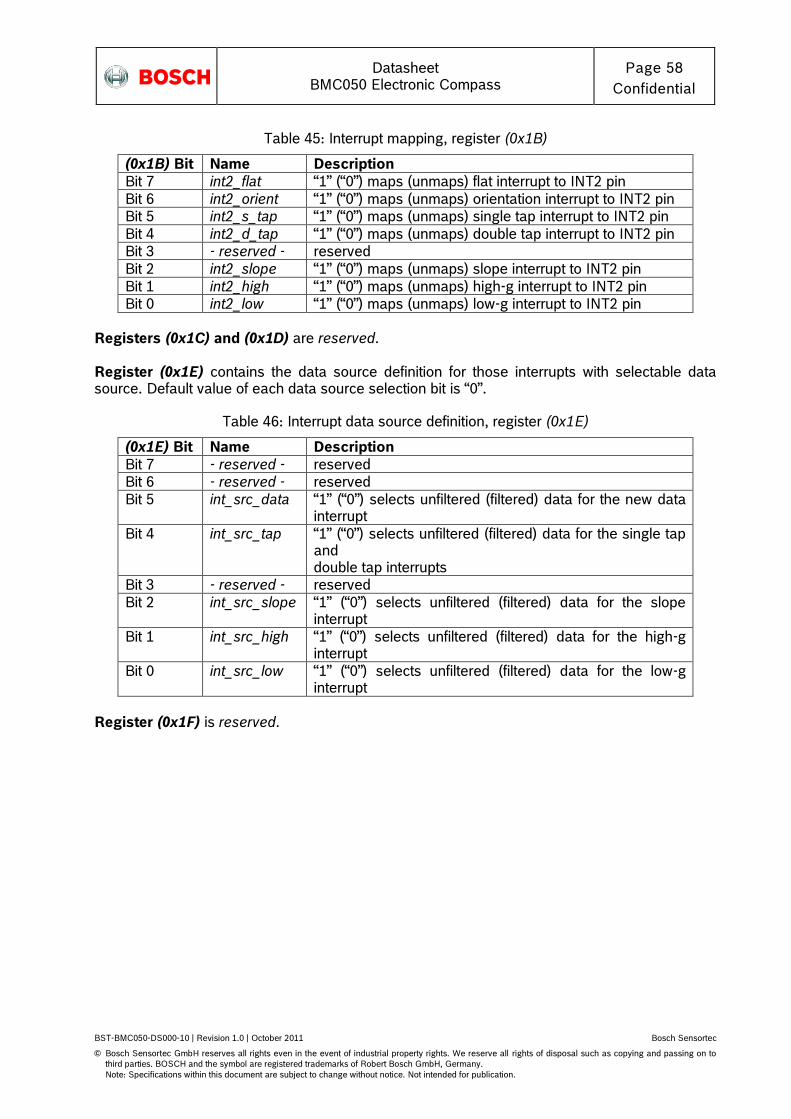
Datasheet
BMC050 Electronic Compass Page 58
Confidential
BST-BMC050-DS000-10 | Revision 1.0 | October 2011 Bosch Sensortec
© Bosch Sensortec GmbH reserves all rights even in the event of industrial property rights. We reserve all rights of disposal such as copying and passing on to
third parties. BOSCH and the symbol are registered trademarks of Robert Bosch GmbH, Germany.
Note: Specifications within this document are subject to change without notice. Not intended for publication.
Table 45: Interrupt mapping, register (0x1B)
(0x1B) Bit Name Description
Bit 7 int2_flat “1” (“0”) maps (unmaps) flat interrupt to INT2 pin
Bit 6 int2_orient “1” (“0”) maps (unmaps) orientation interrupt to INT2 pin
Bit 5 int2_s_tap “1” (“0”) maps (unmaps) single tap interrupt to INT2 pin
Bit 4 int2_d_tap “1” (“0”) maps (unmaps) double tap interrupt to INT2 pin
Bit 3 - reserved - reserved
Bit 2 int2_slope “1” (“0”) maps (unmaps) slope interrupt to INT2 pin
Bit 1 int2_high “1” (“0”) maps (unmaps) high-g interrupt to INT2 pin
Bit 0 int2_low “1” (“0”) maps (unmaps) low-g interrupt to INT2 pin
Registers (0x1C) and (0x1D) are reserved. Register (0x1E) contains the data source definition for those interrupts with selectable data source. Default value of each data source selection bit is “0”.
Table 46: Interrupt data source definition, register (0x1E)
(0x1E) Bit Name Description
Bit 7 - reserved - reserved
Bit 6 - reserved - reserved
Bit 5 int_src_data “1” (“0”) selects unfiltered (filtered) data for the new data interrupt
Bit 4 int_src_tap “1” (“0”) selects unfiltered (filtered) data for the single tap and double tap interrupts
Bit 3 - reserved - reserved
Bit 2 int_src_slope “1” (“0”) selects unfiltered (filtered) data for the slope interrupt
Bit 1 int_src_high “1” (“0”) selects unfiltered (filtered) data for the high-g interrupt
Bit 0 int_src_low “1” (“0”) selects unfiltered (filtered) data for the low-g interrupt
Register (0x1F) is reserved.

Datasheet
BMC050 Electronic Compass Page 59
Confidential
BST-BMC050-DS000-10 | Revision 1.0 | October 2011 Bosch Sensortec
© Bosch Sensortec GmbH reserves all rights even in the event of industrial property rights. We reserve all rights of disposal such as copying and passing on to
third parties. BOSCH and the symbol are registered trademarks of Robert Bosch GmbH, Germany.
Note: Specifications within this document are subject to change without notice. Not intended for publication.
Register (0x20) contains the behavioural configuration (electrical behaviour) of the interrupt pins. Default value of (0x20) int1_od and (0x20) int2_od is “0”. Default value of (0x20) int1_lvl and (0x20) int2_lvl is “1”.
Table 47: Electrical behaviour of interrupt pin, register (0x20)
(0x20) Bit Name Description
Bit 7 - reserved - reserved
Bit 6 - reserved - reserved
Bit 5 - reserved - reserved
Bit 4 - reserved - reserved
Bit 3 int2_od “0” selects push-pull, “1” selects open drive for INT2 pin
Bit 2 int2_lvl “0” (“1”) selects active level “0” (“1”) for INT2 pin
Bit 1 int1_od “0” selects push-pull, “1” selects open drive for INT1
Bit 0 int1_lvl “0” (“1”) selects active level “0” (“1”) for INT1 pin
Register (0x21) contains the interrupt reset bit and the interrupt mode selection. Writing “1” to (0x21) reset_int resets any latched interrupt. The settings for (0x21) latch_int are “0000b” (non-latched), “0001b” (temporary, 250 ms), “0010b” (temporary, 500 ms), “0011b” (temporary, 1 s), ”0100b” (temporary, 2 s), ”0101b” (temporary, 4 s), ”0110b” (temporary, 8 s), ”0111b” (latched), ”1000b” (non-latched), ”1001b”
(temporary, 500 s), ”1010b” (temporary, 500 s), ”1011b” (temporary, 1 ms), ”1100b” (temporary, 12.5 ms), ”1101b” (temporary, 25 ms), ”1110b” (temporary, 50 ms), ”1111b” (latched). Default value of (0x21) latch_int is ”0000b”.
Table 48: Interrupt reset bit and interrupt mode selection, register (0x21)
Bit 7 Bit 6 Bit 5 Bit 4 Bit 3 Bit 2 Bit 1 Bit 0
reset_int reserved reserved reserved latch_ int<3>
latch_ int<2>
latch_ int<1>
latch_ int<0>
Register (0x22) contains the delay time definition for the low-g interrupt. The physical delay time can be computed from the content of (0x22) low_dur according to: delay [ms] = [(0x22) low_dur + 1] • 2 ms. Possible delay times range from 2 ms to 512 ms. Default value of (0x22) low_dur is 0x09, corresponding to a delay of 20 ms.
Table 49: Delay time definition for the low-g interrupt, register (0x22)
Bit 7 Bit 6 Bit 5 Bit 4 Bit 3 Bit 2 Bit 1 Bit 0
low_ dur<7>
low_ dur<6>
low_ dur<5>
low_ dur<4>
low_ dur<3>
low_ dur<2>
low_ dur<1>
low_ dur<0>

Datasheet
BMC050 Electronic Compass Page 60
Confidential
BST-BMC050-DS000-10 | Revision 1.0 | October 2011 Bosch Sensortec
© Bosch Sensortec GmbH reserves all rights even in the event of industrial property rights. We reserve all rights of disposal such as copying and passing on to
third parties. BOSCH and the symbol are registered trademarks of Robert Bosch GmbH, Germany.
Note: Specifications within this document are subject to change without notice. Not intended for publication.
Register (0x23) contains the threshold definition for the low-g interrupt. An LSB of (0x23) low_th corresponds to an actual acceleration of 7.81 mg. Therefore, the threshold ranges from 0 g to 1.992 g. Default value of (0x23) low_th is 0x30, corresponding to an acceleration of 375 mg.
Table 50: Threshold definition for the low-g interrupt, register (0x23)
Bit 7 Bit 6 Bit 5 Bit 4 Bit 3 Bit 2 Bit 1 Bit 0
low_ th<7>
low_ th<6>
low_ th<5>
low_ th<4>
low_ th<3>
low_ th<2>
low_ th<1>
low_ th<0>
Register (0x24) contains the low-g interrupt mode selection, the low-g interrupt hysteresis setting, and the high-g interrupt hysteresis setting. Setting (0x24) low_mode to ”0” (“1”) selects ´single´ mode (´sum´ mode). Default value is “0” (´single´ mode). (0x24) low_hy sets the hysteresis of the low-g interrupt. An LSB of (0x24) low_hy corresponds to an acceleration difference of 125 mg. Default value of (0x24) low_hy is “01b”. (0x24) high_hy sets the hysteresis of the high-g interrupt. The meaning of an LSB of (0x24) high_hy depends on the selected g-range. It corresponds to an acceleration difference of 125 mg in 2g-range, 250 mg in 4g-range, 500 mg in 8g-range, and 1000mg in 16g-range. Default value of (0x24) high_hy is “10b”.
Table 51: Threshold definition for the low-g interrupt, register (0x24)
Bit 7 Bit 6 Bit 5 Bit 4 Bit 3 Bit 2 Bit 1 Bit 0
high_ hy<1>
high_ hy<0>
reserved reserved reserved low_ mode
low_ hy<1>
low_ hy<0>
Register (0x25) contains the delay time definition for the high-g interrupt. The physical delay time can be computed from the content of (0x25) high_dur according to delay [ms] = [(0x22) high_dur + 1] • 2 ms. Possible delay times range from 2 ms to 512 ms. Default value of (0x25) high_dur is 0x0F, corresponding to a delay of 32 ms.
Table 52: Delay time definition for the high-g interrupt, register (0x25)
Bit 7 Bit 6 Bit 5 Bit 4 Bit 3 Bit 2 Bit 1 Bit 0
high_ dur<7>
high_ dur<6>
high_ dur<5>
high_ dur<4>
high_ dur<3>
high_ dur<2>
high_ dur<1>
high_ dur<0>
Register (0x26) contains the threshold definition for the high-g interrupt. The meaning of an LSB of (0x26) high_th depends on the selected g-range. It corresponds to 7.81 mg in 2g-range, 15.63 mg in 4g-range, 31.25 mg in 8g-range, and 62.5 mg in 16g-range. Default value of (0x26) high_th is 0xC0.
Table 53: Threshold definition for the high-g interrupt, register (0x26)
Bit 7 Bit 6 Bit 5 Bit 4 Bit 3 Bit 2 Bit 1 Bit 0
high_ th<7>
high_ th<6>
high_ th<5>
high_ th<4>
high_ th<3>
high_ th<2>
high_ th<1>
high_ th<0>

Datasheet
BMC050 Electronic Compass Page 61
Confidential
BST-BMC050-DS000-10 | Revision 1.0 | October 2011 Bosch Sensortec
© Bosch Sensortec GmbH reserves all rights even in the event of industrial property rights. We reserve all rights of disposal such as copying and passing on to
third parties. BOSCH and the symbol are registered trademarks of Robert Bosch GmbH, Germany.
Note: Specifications within this document are subject to change without notice. Not intended for publication.
Register (0x27) contains the definition of the number of samples to be evaluated for the slope interrupt (any-motion detection). The number of samples is N = (0x27) slope_dur + 1. Default value of (0x27) slope_dur is “00b”.
Table 54: Samples number definition for the slope interrupt, register (0x27)
Bit 7 Bit 6 Bit 5 Bit 4 Bit 3 Bit 2 Bit 1 Bit 0
reserved reserved reserved reserved reserved reserved slope_ dur<1>
slope_ dur<0>
Register (0x28) contains the threshold definition for the slope interrupt. An LSB of (0x28) slope_th corresponds to an LSB of acceleration data. Its meaning therefore depends on the selected g-range. Default value of (0x28) slope_th is 0x14.
Table 55: Samples number definition for the slope interrupt, register (0x28)
Bit 7 Bit 6 Bit 5 Bit 4 Bit 3 Bit 2 Bit 1 Bit 0
slope_ th<7>
slope_ th<6>
slope_ th<5>
slope_ th<4>
slope_ th<3>
slope_ th<2>
slope_ th<1>
slope_ th<0>
Register (0x29) is reserved. Register (0x2A) contains the timing definitions for the single tap and double tap interrupts. (0x2A) tap_quiet = “0” (“1”) selects a quiet duration of 30 ms (20 ms). The default value of (0x2A) tap_quiet is “0”. (0x2A) tap_shock = “0” (“1”) selects a shock duration of 50 ms (75 ms). The default value of (0x2A) tap_shock is “0”. (0x2A) tap_dur selects the length of the time window for the second shock event (for double tap detection). The settings for (0x2A) tap_dur are “000b” (50 ms), “001b” (100 ms), “010b” (150 ms), “011b” (200 ms), “100b” (250 ms), “101b” (375 ms), “110b” (500 ms), “111b” (700 ms). The default value of (0x2A) tap_dur is “100b”.
Table 56: Tap Quiet duration and tap shock duration, register (0x2A)
Bit 7 Bit 6 Bit 5 Bit 4 Bit 3 Bit 2 Bit 1 Bit 0
tap_ quiet
tap_ shock
reserved reserved reserved tap_ dur<2>
tap_ dur<1>
tap_ dur<0>
Register (0x2B) contains the definition of the number of samples to be processed after wake-up in low-power mode and the threshold definition for the single and double tap interrupts. (0x2B) tap_samp selects the number of samples that are processed after wake-up in the low-power mode. The settings for (0x2B) tap_samp are “00b” (2 samples), “01b” (4 samples), “10b” (8 samples), and “11b” (16 samples). Default value of (0x2B) tap_samp is “00b”.

Datasheet
BMC050 Electronic Compass Page 62
Confidential
BST-BMC050-DS000-10 | Revision 1.0 | October 2011 Bosch Sensortec
© Bosch Sensortec GmbH reserves all rights even in the event of industrial property rights. We reserve all rights of disposal such as copying and passing on to
third parties. BOSCH and the symbol are registered trademarks of Robert Bosch GmbH, Germany.
Note: Specifications within this document are subject to change without notice. Not intended for publication.
The meaning of an LSB of (0x2B) tap_th depends on the selected g-range. It corresponds to an acceleration difference of 62.5mg in 2g-range, 125mg in 4g-range, 250mg in 8g-range, and 500mg in 16g-range. Default value of (0x2B) tap_th is 0x0A.
Table 57: Samples number after wake-up and threshold tap interrupt, register (0x2B)
Bit 7 Bit 6 Bit 5 Bit 4 Bit 3 Bit 2 Bit 1 Bit 0
tap_ samp<1>
tap_ samp<0>
reserved tap_ th<4>
tap_ th<3>
tap_ th<2>
tap_ th<1>
tap_ th<0>
Register (0x2C) contains the definition of hysteresis, blocking, and mode for the orientation interrupt. (0x2C) orient_hyst sets the hysteresis of the orientation interrupt; 1 LSB always corresponds to 62.5 mg, in any g-range (i.e. increment is independent from g-range setting). Default value of (0x2C) orient_hyst is “001b”. (0x2C) orient_blocking selects the kind of blocking that is used for the generation of the orientation interrupt. The settings for (0x2C) orient_blocking are “00b” (no blocking), “01b” (theta blocking), “10b” (theta blocking or slope in any axis > 0.2 g), and “11b” (orient value not stable for at least 100 ms or theta blocking or slope in any axis > 0.4 g). Default value of (0x2C) orient_blocking is “10b”. (0x2C) orient_mode sets the thresholds for switching between the different orientations. The settings for (0x2C) orient_mode are “00b” (symmetrical), “01b” (high-asymmetrical), “10b” (low-asymmetrical), “11b” (symmetrical). Default value of (0x2C) orient_mode is “00b”.
Table 58: Hysteresis, Blocking for Orientation Interrupt, Register (0x2C)
Bit 7 Bit 6 Bit 5 Bit 4 Bit 3 Bit 2 Bit 1 Bit 0
reserved orient_ hyst<2
>
orient_ hyst<1
>
orient_ hyst<0
>
orient_ blocking<1>
orient_ blocking<0>
orient_ mode<1
>
orient_ mode<0
>
Register (0x2D) contains the definition of the theta blocking angle for the orientation interrupt. (0x2D) orient_theta defines a blocking angle between 0° and 44.8° as described in chapter 4.8.7.1. Default value of (0x2D) orient_theta is 0x08.
Table 59: Theta blocking angle, register (0x2D)
Bit 7 Bit 6 Bit 5 Bit 4 Bit 3 Bit 2 Bit 1 Bit 0
reserved reserved orient_ theta<5>
orient_ theta<4>
orient_ theta<3>
orient_ theta<2>
orient_ theta<1>
orient_ theta<0>
Register (0x2E) contains the definition of the flat threshold angle for the flat interrupt. (0x2E) flat_theta defines a blocking angle between 0° and 44.8° as described in chapter 4.8.8. Default value of (0x2E) flat_theta is 0x08.
Table 60: Flat threshold angle, register (0x2E)
Bit 7 Bit 6 Bit 5 Bit 4 Bit 3 Bit 2 Bit 1 Bit 0
reserved reserved flat_ theta<5>
flat_ theta<4>
flat_ theta<3>
flat_ theta<2>
flat_ theta<1>
flat_ theta<0>

Datasheet
BMC050 Electronic Compass Page 63
Confidential
BST-BMC050-DS000-10 | Revision 1.0 | October 2011 Bosch Sensortec
© Bosch Sensortec GmbH reserves all rights even in the event of industrial property rights. We reserve all rights of disposal such as copying and passing on to
third parties. BOSCH and the symbol are registered trademarks of Robert Bosch GmbH, Germany.
Note: Specifications within this document are subject to change without notice. Not intended for publication.
Register (0x2F) contains the definition of the flat hold time. (0x2F) flat_hold_time defines the time a new flat value has to be at least stable for before the interrupt is generated. The settings for (0x2F) flat_hold_time are “00b” (0), “01b” (512 ms), “10b” (1024 ms), “11b” (2048 ms). Default value of (0x2F) flat_hold_time is “01b”.
Table 61: Flat threshold angle, register (0x2F)
Bit 7 Bit 6 Bit 5 Bit 4 Bit 3 Bit 2 Bit 1 Bit 0
reserved reserved flat_hold_ time<1>
flat_hold_ time<0>
reserved reserved reserved reserved
Register (0x30) and (0x31) are reserved.

Datasheet
BMC050 Electronic Compass Page 64
Confidential
BST-BMC050-DS000-10 | Revision 1.0 | October 2011 Bosch Sensortec
© Bosch Sensortec GmbH reserves all rights even in the event of industrial property rights. We reserve all rights of disposal such as copying and passing on to
third parties. BOSCH and the symbol are registered trademarks of Robert Bosch GmbH, Germany.
Note: Specifications within this document are subject to change without notice. Not intended for publication.
5.12 Self-test
Register (0x32) contains the settings for the activation of the sensor self-test. (0x32) self_test_sign sets the sign of the electrostatic excitation. The settings for (0x32) self_test_sign are “0” (positive sign) and “1” (negative sign). Default value of (0x32) self_test_sign is “0”. (0x32) self_test_axis defines the axis which shall be excited. Only one axis can be excited at the same time. The settings for (0x32) self_test_axis are “00b” (no self-test), “01” (x-axis), “10” (y-axis), and “11” (z-axis). Default value of (0x32) self_test_axis is “00b”.
Table 62: Sensor self-test, register (0x32)
Bit 7 Bit 6 Bit 5 Bit 4 Bit 3 Bit 2 Bit 1 Bit 0
reserved reserved reserved reserved reserved self_test _sign
self_test _axis<1>
self_test _axis<0>
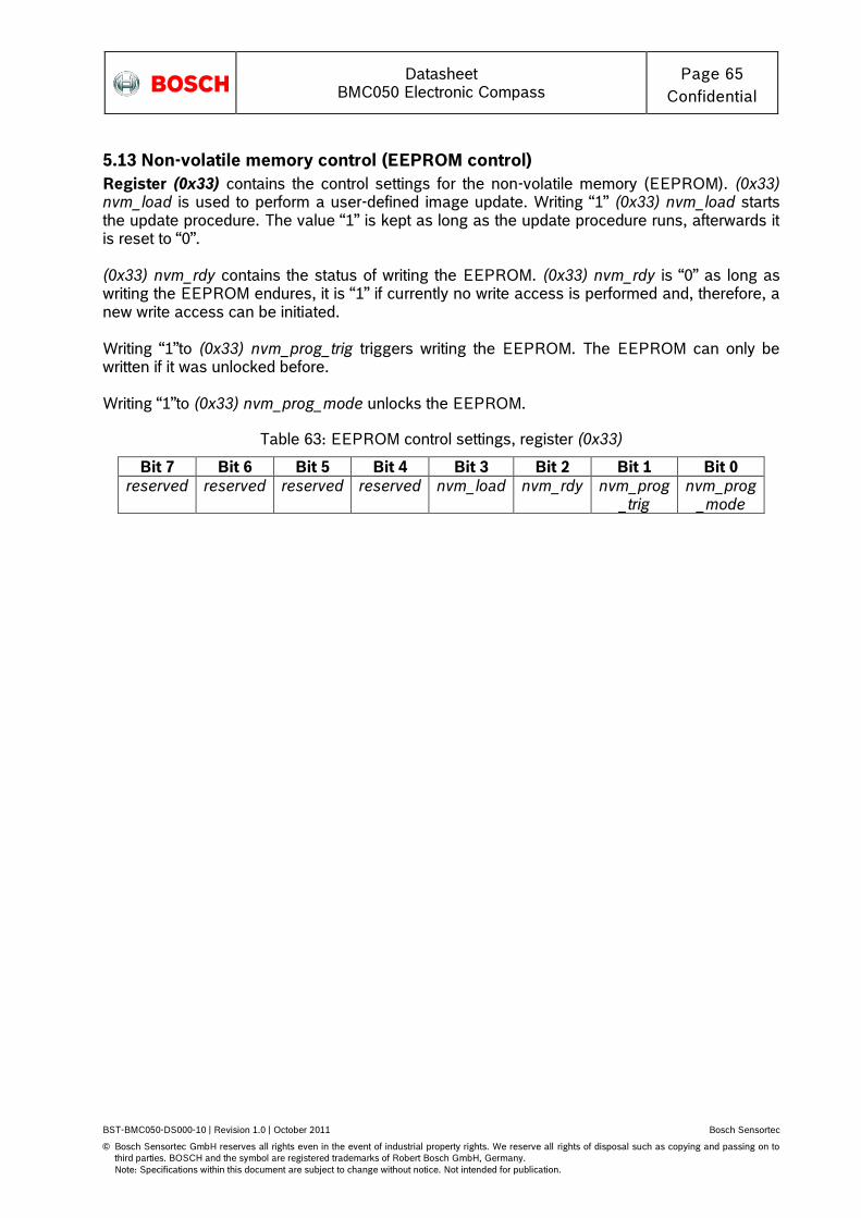
Datasheet
BMC050 Electronic Compass Page 65
Confidential
BST-BMC050-DS000-10 | Revision 1.0 | October 2011 Bosch Sensortec
© Bosch Sensortec GmbH reserves all rights even in the event of industrial property rights. We reserve all rights of disposal such as copying and passing on to
third parties. BOSCH and the symbol are registered trademarks of Robert Bosch GmbH, Germany.
Note: Specifications within this document are subject to change without notice. Not intended for publication.
5.13 Non-volatile memory control (EEPROM control)
Register (0x33) contains the control settings for the non-volatile memory (EEPROM). (0x33) nvm_load is used to perform a user-defined image update. Writing “1” (0x33) nvm_load starts the update procedure. The value “1” is kept as long as the update procedure runs, afterwards it is reset to “0”. (0x33) nvm_rdy contains the status of writing the EEPROM. (0x33) nvm_rdy is “0” as long as writing the EEPROM endures, it is “1” if currently no write access is performed and, therefore, a new write access can be initiated. Writing “1”to (0x33) nvm_prog_trig triggers writing the EEPROM. The EEPROM can only be written if it was unlocked before. Writing “1”to (0x33) nvm_prog_mode unlocks the EEPROM.
Table 63: EEPROM control settings, register (0x33)
Bit 7 Bit 6 Bit 5 Bit 4 Bit 3 Bit 2 Bit 1 Bit 0
reserved reserved reserved reserved nvm_load nvm_rdy nvm_prog _trig
nvm_prog _mode

Datasheet
BMC050 Electronic Compass Page 66
Confidential
BST-BMC050-DS000-10 | Revision 1.0 | October 2011 Bosch Sensortec
© Bosch Sensortec GmbH reserves all rights even in the event of industrial property rights. We reserve all rights of disposal such as copying and passing on to
third parties. BOSCH and the symbol are registered trademarks of Robert Bosch GmbH, Germany.
Note: Specifications within this document are subject to change without notice. Not intended for publication.
5.14 Interface configuration
Register (0x34) contains the settings for the digital interfaces. Writing “1” to (0x34) i2c_wdt_en enables the watchdog at the SDI pin (= SDA for I²C) if I²C is selected. Default value of (0x34) i2c_wdt_en is “0”. (0x34) i2c_wdt_sel selects the I²C data pad watchdog timer period. The settings for (0x34) i2c_wdt_sel are “0” (1 ms) and “1” (50 ms). Default value of (0x34) i2c_wdt_sel is “0”. (0x34) spi3 selects the SPI mode. The settings for (0x34) spi3 are “0” (4-wire SPI) and “1” (3-wire SPI). Default value of (0x34) spi3 is “0”.
Table 64: EEPROM control settings, register (0x34)
Bit 7 Bit 6 Bit 5 Bit 4 Bit 3 Bit 2 Bit 1 Bit 0
reserved reserved reserved reserved reserved i2c_wdt _en
i2c_wdt _sel
spi3
Register (0x35) is reserved.

Datasheet
BMC050 Electronic Compass Page 67
Confidential
BST-BMC050-DS000-10 | Revision 1.0 | October 2011 Bosch Sensortec
© Bosch Sensortec GmbH reserves all rights even in the event of industrial property rights. We reserve all rights of disposal such as copying and passing on to
third parties. BOSCH and the symbol are registered trademarks of Robert Bosch GmbH, Germany.
Note: Specifications within this document are subject to change without notice. Not intended for publication.
5.15 Offset compensation
Register (0x36) contains settings for the offset compensation in general, for fast offset compensation, and for slow offset compensation. Writing “1”to (0x36) offset_reset sets all offset compensation registers (0x38 to 0x3D) to zero. Default value of (0x36) offset_reset is “0”. (0x36) cal_trigger starts the fast compensation process for the specified axis. The settings for (0x36) cal_trigger are “00b” (no axis selected), “01b” (x-axis), “10b” (y-axis), “11b” (z-axis). A non-zero value is kept until the fast compensation procedure is finished. Default value of (0x36) cal_trigger is “00b”. (0x36) cal_rdy indicates the state of the fast compensation. (0x36) cal_rdy is “0” when (0x36) cal_trigger has a nonzero value, otherwise (0x36) cal_rdy is “1”. Writing “1” (“0”) to (0x36) hp_z_en enables (disables) slow offset compensation for the z-axis. Writing “1” (“0”) to (0x36) hp_y_en enables (disables) slow offset compensation for the y-axis. Writing “1” (“0”) to (0x36) hp_x_en enables (disables) slow offset compensation for the x-axis. Default value for each of (0x36) hp_x_en, (0x36) hp_y_en, and (0x36) hp_x_en is “0”, respectively.
Table 65: Offset compensation, fast offset compensation, register (0x36)
Bit 7 Bit 6 Bit 5 Bit 4 Bit 3 Bit 2 Bit 1 Bit 0
offset _reset
cal_ trigger<1>
cal_ trigger<0>
cal_rdy reserved hp_z_en hp_y_en hp_x_en
Register (0x37) contains settings for the offset compensation in general, and for slow offset compensation. (0x37) offset_target_z sets the target value for the offset compensation of the z-axis. (0x37) offset_target_y sets the target value for the offset compensation of the y-axis. (0x37) offset_target_x sets the target value for the offset compensation of the x-axis. The settings for (0x37) offset_target_x, (0x37) offset_target_y, and (0x37) offset_target_z are “00b” (0 g), “01b” (+1 g), “10b” (-1 g), and “11b” (0 g). Default value of each of (0x37) offset_target_x, (0x37) offset_target_y, and (0x37) offset_target_z is “00b”, respectively. (0x37) cut_off defines the number of samples for comparison by the slow offset compensation. The settings for (0x37) cut_off are “0” (8 samples) and “1” (16 samples). The default value of (0x37) cut_off is “0”.
Table 66: Offset compensation, slow offset compensation, register (0x37)
Bit 7 Bit 6 Bit 5 Bit 4 Bit 3 Bit 2 Bit 1 Bit 0
reserved
offset_target_z<
1>
offset_target_z<
0>
offset_target_y<
1>
offset_target_y<
0>
offset_target_x<
1>
offset_target_x<
0>
cut_off
Register (0x38) contains the compensation value for filtered data for the x-axis. The contents of each of the registers (0x38) to (0x3D) is added to the corresponding acceleration data; it can be set either automatically by one of the implemented compensation algorithms or manually. These
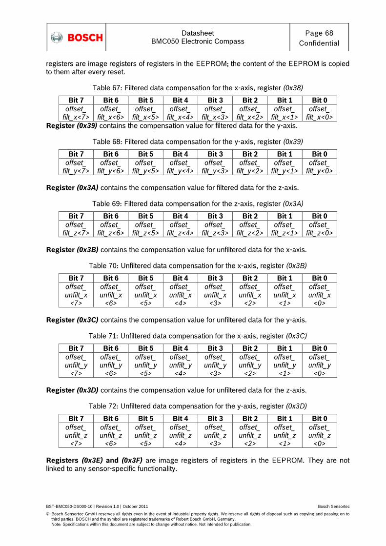
Datasheet
BMC050 Electronic Compass Page 68
Confidential
BST-BMC050-DS000-10 | Revision 1.0 | October 2011 Bosch Sensortec
© Bosch Sensortec GmbH reserves all rights even in the event of industrial property rights. We reserve all rights of disposal such as copying and passing on to
third parties. BOSCH and the symbol are registered trademarks of Robert Bosch GmbH, Germany.
Note: Specifications within this document are subject to change without notice. Not intended for publication.
registers are image registers of registers in the EEPROM; the content of the EEPROM is copied to them after every reset.
Table 67: Filtered data compensation for the x-axis, register (0x38)
Bit 7 Bit 6 Bit 5 Bit 4 Bit 3 Bit 2 Bit 1 Bit 0
offset_ filt_x<7>
offset_ filt_x<6>
offset_ filt_x<5>
offset_ filt_x<4>
offset_ filt_x<3>
offset_ filt_x<2>
offset_ filt_x<1>
offset_ filt_x<0>
Register (0x39) contains the compensation value for filtered data for the y-axis.
Table 68: Filtered data compensation for the y-axis, register (0x39)
Bit 7 Bit 6 Bit 5 Bit 4 Bit 3 Bit 2 Bit 1 Bit 0
offset_ filt_y<7>
offset_ filt_y<6>
offset_ filt_y<5>
offset_ filt_y<4>
offset_ filt_y<3>
offset_ filt_y<2>
offset_ filt_y<1>
offset_ filt_y<0>
Register (0x3A) contains the compensation value for filtered data for the z-axis.
Table 69: Filtered data compensation for the z-axis, register (0x3A)
Bit 7 Bit 6 Bit 5 Bit 4 Bit 3 Bit 2 Bit 1 Bit 0
offset_ filt_z<7>
offset_ filt_z<6>
offset_ filt_z<5>
offset_ filt_z<4>
offset_ filt_z<3>
offset_ filt_z<2>
offset_ filt_z<1>
offset_ filt_z<0>
Register (0x3B) contains the compensation value for unfiltered data for the x-axis.
Table 70: Unfiltered data compensation for the x-axis, register (0x3B)
Bit 7 Bit 6 Bit 5 Bit 4 Bit 3 Bit 2 Bit 1 Bit 0
offset_ unfilt_x
<7>
offset_ unfilt_x
<6>
offset_ unfilt_x
<5>
offset_ unfilt_x
<4>
offset_ unfilt_x
<3>
offset_ unfilt_x
<2>
offset_ unfilt_x
<1>
offset_ unfilt_x
<0>
Register (0x3C) contains the compensation value for unfiltered data for the y-axis.
Table 71: Unfiltered data compensation for the x-axis, register (0x3C)
Bit 7 Bit 6 Bit 5 Bit 4 Bit 3 Bit 2 Bit 1 Bit 0
offset_ unfilt_y
<7>
offset_ unfilt_y
<6>
offset_ unfilt_y
<5>
offset_ unfilt_y
<4>
offset_ unfilt_y
<3>
offset_ unfilt_y
<2>
offset_ unfilt_y
<1>
offset_ unfilt_y
<0>
Register (0x3D) contains the compensation value for unfiltered data for the z-axis.
Table 72: Unfiltered data compensation for the y-axis, register (0x3D)
Bit 7 Bit 6 Bit 5 Bit 4 Bit 3 Bit 2 Bit 1 Bit 0
offset_ unfilt_z
<7>
offset_ unfilt_z
<6>
offset_ unfilt_z
<5>
offset_ unfilt_z
<4>
offset_ unfilt_z
<3>
offset_ unfilt_z
<2>
offset_ unfilt_z
<1>
offset_ unfilt_z
<0>
Registers (0x3E) and (0x3F) are image registers of registers in the EEPROM. They are not linked to any sensor-specific functionality.

Datasheet
BMC050 Electronic Compass Page 69
Confidential
BST-BMC050-DS000-10 | Revision 1.0 | October 2011 Bosch Sensortec
© Bosch Sensortec GmbH reserves all rights even in the event of industrial property rights. We reserve all rights of disposal such as copying and passing on to
third parties. BOSCH and the symbol are registered trademarks of Robert Bosch GmbH, Germany.
Note: Specifications within this document are subject to change without notice. Not intended for publication.
6. Magnetometer register description
6.1 General remarks
The entire communication with the device‟s magnetometer part is performed by reading from and writing to registers. Registers have a width of 8 bits; they are mapped to a common space of 50 addresses from (0x40) up to (0x71). Within the used range there are several registers which are marked as „reserved‟. Any reserved bit is ignored when it is written and no specific value is guaranteed when read. Especially, in SPI mode the SDO pin may stay in high-Z state when reading some of these registers. Registers with addresses from (0x40) up to (0x4A) are read-only. Any attempt to write to these registers is ignored.
6.2 Register map
Register Address Default Value bit7 bit6 bit5 bit4 bit3 bit2 bit1 bit0
0x71 N/A
0x70 N/A
0x6F N/A
0x6E N/A
0x6D N/A
0x6C N/A
0x6B N/A
0x6A N/A
0x69 N/A
0x68 N/A
0x67 N/A
0x66 N/A
0x65 N/A
0x64 N/A
0x63 N/A
0x62 N/A
0x61 N/A
0x60 N/A
0x5F N/A
0x5E N/A
0x5D N/A
0x5C N/A
0x5B N/A
0x5A N/A
0x59 N/A
0x58 N/A
0x57 N/A
0x56 N/A
0x55 N/A
0x54 N/A
0x53 N/A
0x52 0x00
0x51 0x00
0x50 0x00
0x4F 0x00
0x4E 0x07 Data Ready Pin En Interrupt Pin En Channel Z Channel Y Channel X DR Polarity Interrupt Latch Interrupt Polarity
0X4D 0x3F Data Overrun En Overflow Int En High Int Z en High Int Y en High Int X en Low Int Z en Low Int Y en Low Int X en
0x4C 0x06 Self Test
0x4B 0x01 Soft Reset '1' fixed '0' fixed '0' fixed '0' fixed '0' SPI3en Soft Reset '1' Power Control Bit
0x4A 0x00 Data Overrun Overflow High Int Z High Int Y High Int X Low Int Z Low Int Y Low Int X
0x49 N/A
0x48 N/A fixed '0' Data Ready Status
0x47 N/A
0x46 N/A Z-Self-Test
0x45 N/A
0x44 N/A fixed '0' fixed '0' Y-Self-Test
0x43 N/A
0x42 N/A fixed '0' fixed '0' X-Self-Test
0x41 N/A
0x40 0x32
w/r
w/r accessible
in suspend mode
read only
reserved
reserved
reserved
Chip ID = 0x32 (can only be read if power control bit ="1")
REPZ Number Of Repetitions (valid for Z) [7:0]
REPXY Number Of Repetitions (valid for XY) [7:0]
DATA X [12:5] MSB
DATA X [4:0] LSB
DATA Z [14:7] MSB
RHALL [5:0] LSB
DATA Y [12:5] MSB
DATA Y [4:0] LSB
High Threshold [7:0]
Low Threshold [7:0]
Adv. ST [1:0] Data Rate [2:0]
DATA Z [6:0] LSB
Opmode [1:0]
RHALL [13:6] MSB

Datasheet
BMC050 Electronic Compass Page 70
Confidential
BST-BMC050-DS000-10 | Revision 1.0 | October 2011 Bosch Sensortec
© Bosch Sensortec GmbH reserves all rights even in the event of industrial property rights. We reserve all rights of disposal such as copying and passing on to
third parties. BOSCH and the symbol are registered trademarks of Robert Bosch GmbH, Germany.
Note: Specifications within this document are subject to change without notice. Not intended for publication.
6.3 Chip ID
Register (0x40) Chip ID contains the magnetometer chip identification number, which is 0x32. This number can only be read if the power control bit (register 0x4B bit0) is enabled.
Table 73: Chip identification number, register (0x40)
Bit 7 Bit 6 Bit 5 Bit 4 Bit 3 Bit 2 Bit 1 Bit 0
0 0 1 1 0 0 1 0
Register (0x01) is reserved
6.4 Magnetic field data
Register (0x42) contains the LSB part of x-axis magnetic field data and the self-test result flag for the x-axis.
Table 74: LSB part of x-axis magnetic field, register (0x42)
(0x42) Bit Name Description
Bit 7 DATAX_lsb <4> Bit 4 of x-axis magnetic field data
Bit 6 DATAX_lsb <3> Bit 3 of x-axis magnetic field data
Bit 5 DATAX_lsb <2> Bit 2 of x-axis magnetic field data
Bit 4 DATAX_lsb <1> Bit 1 of x-axis magnetic field data
Bit 3 DATAX_lsb <0> Bit 0 of x-axis magnetic field data = x LSB
Bit 2 - (fixed to 0)
Bit 1 - (fixed to 0)
Bit 0 SelfTestX Self-test result flag for x-axis, default is “1”
Register (0x43) contains the MSB part of x-axis magnetic field data.
Table 75: MSB part of x-axis magnetic field, register (0x43)
(0x43) Bit
Name Description
Bit 7 DATAX_msb <12> Bit 12 of x-axis magnetic field data = x MSB
Bit 6 DATAX_msb <11> Bit 11 of x-axis magnetic field data
Bit 5 DATAX_msb <10> Bit 10 of x-axis magnetic field data
Bit 4 DATAX_msb <9> Bit 9 of x-axis magnetic field data
Bit 3 DATAX_msb <8> Bit 8 of x-axis magnetic field data
Bit 2 DATAX_msb <7> Bit 7 of x-axis magnetic field data
Bit 1 DATAX_msb <6> Bit 6 of x-axis magnetic field data
Bit 0 DATAX_msb <5> Bit 5 of x-axis magnetic field data

Datasheet
BMC050 Electronic Compass Page 71
Confidential
BST-BMC050-DS000-10 | Revision 1.0 | October 2011 Bosch Sensortec
© Bosch Sensortec GmbH reserves all rights even in the event of industrial property rights. We reserve all rights of disposal such as copying and passing on to
third parties. BOSCH and the symbol are registered trademarks of Robert Bosch GmbH, Germany.
Note: Specifications within this document are subject to change without notice. Not intended for publication.
Register (0x44) contains the LSB part of y-axis magnetic field data and the self-test result flag for the y-axis.
Table 76: LSB part of y-axis magnetic field, register (0x44)
(0x44) Bit Name Description
Bit 7 DATAY_lsb <4> Bit 4 of y-axis magnetic field data
Bit 6 DATAY_lsb <3> Bit 3 of y-axis magnetic field data
Bit 5 DATAY_lsb <2> Bit 2 of y-axis magnetic field data
Bit 4 DATAY_lsb <1> Bit 1 of y-axis magnetic field data
Bit 3 DATAY_lsb <0> Bit 0 of y-axis magnetic field data = y LSB
Bit 2 - (fixed to 0)
Bit 1 - (fixed to 0)
Bit 0 SelfTestY Self-test result flag for y-axis, default is “1”
Register (0x45) contains the MSB part of y-axis magnetic field data.
Table 77: MSB part of y-axis magnetic field, register (0x45)
(0x43) Bit
Name Description
Bit 7 DATAY_msb <12> Bit 12 of y-axis magnetic field data = y MSB
Bit 6 DATAY_msb <11> Bit 11 of y-axis magnetic field data
Bit 5 DATAY_msb <10> Bit 10 of y-axis magnetic field data
Bit 4 DATAY_msb <9> Bit 9 of y-axis magnetic field data
Bit 3 DATAY_msb <8> Bit 8 of y-axis magnetic field data
Bit 2 DATAY_msb <7> Bit 7 of y-axis magnetic field data
Bit 1 DATAY_msb <6> Bit 6 of y-axis magnetic field data
Bit 0 DATAY_msb <5> Bit 5 of y-axis magnetic field data
Register (0x46) contains the LSB part of z-axis magnetic field data and the self-test result flag for the z-axis.
Table 78: LSB part of z-axis magnetic field, register (0x44)
(0x44) Bit Name Description
Bit 7 DATAZ_lsb <6> Bit 6 of z-axis magnetic field data
Bit 6 DATAZ_lsb <5> Bit 5 of z-axis magnetic field data
Bit 5 DATAZ_lsb <4> Bit 4 of z-axis magnetic field data
Bit 4 DATAZ_lsb <3> Bit 3 of z-axis magnetic field data
Bit 3 DATAZ_lsb <2> Bit 2 of z-axis magnetic field data
Bit 2 DATAZ_lsb <1> Bit 1 of z-axis magnetic field data
Bit 1 DATAZ_lsb <0> Bit 0 of z-axis magnetic field data = z LSB
Bit 0 SelfTestZ Self-test result flag for z-axis, default is “1”

Datasheet
BMC050 Electronic Compass Page 72
Confidential
BST-BMC050-DS000-10 | Revision 1.0 | October 2011 Bosch Sensortec
© Bosch Sensortec GmbH reserves all rights even in the event of industrial property rights. We reserve all rights of disposal such as copying and passing on to
third parties. BOSCH and the symbol are registered trademarks of Robert Bosch GmbH, Germany.
Note: Specifications within this document are subject to change without notice. Not intended for publication.
Register (0x47) contains the MSB part of z-axis magnetic field data.
Table 79: MSB part of z-axis magnetic field, register (0x45)
(0x45) Bit
Name Description
Bit 7 DATAZ_lsb <14> Bit 14 of y-axis magnetic field data = z MSB
Bit 6 DATAZ_lsb <13> Bit 13 of y-axis magnetic field data
Bit 5 DATAZ_lsb <12> Bit 12 of y-axis magnetic field data
Bit 4 DATAZ_lsb <11> Bit 11 of y-axis magnetic field data
Bit 3 DATAZ_lsb <10> Bit 10 of y-axis magnetic field data
Bit 2 DATAZ_lsb <9> Bit 9 of y-axis magnetic field data
Bit 1 DATAZ_lsb <8> Bit 8 of y-axis magnetic field data
Bit 0 DATAZ_lsb <7> Bit 7 of y-axis magnetic field data
Register (0x48) contains the LSB part of hall resistance and the Data Ready (DRDY) status bit.
Table 80: LSB part of hall resistance, register (0x46)
(0x46) Bit Name Description
Bit 7 RHALL_lsb <5> Bit 5 of hall resistance
Bit 6 RHALL _lsb <4> Bit 4 of hall resistance
Bit 5 RHALL _lsb <3> Bit 3 of hall resistance
Bit 4 RHALL _lsb <2> Bit 2 of hall resistance
Bit 3 RHALL _lsb <1> Bit 1 of hall resistance
Bit 2 RHALL _lsb <0> Bit 0 of hall resistance = RHALL LSB
Bit 1 - (fixed to 0)
Bit 0 Data Ready Status Data ready (DRDY) status bit
Register (0x49) contains the MSB part of hall resistance.
Table 81: MSB part of hall resistance, register (0x47)
(0x47) Bit
Name Description
Bit 7 RHALL_msb <13> Bit 13 of hall resistance = RHALL MSB
Bit 6 RHALL_msb <12> Bit 12 of hall resistance
Bit 5 RHALL_msb <11> Bit 11 of hall resistance
Bit 4 RHALL_msb <10> Bit 10 of hall resistance
Bit 3 RHALL_msb <9> Bit 9 of hall resistance
Bit 2 RHALL_msb <8> Bit 8 of hall resistance
Bit 1 RHALL_msb <7> Bit 7 of hall resistance
Bit 0 RHALL_msb <6> Bit 6 of hall resistance
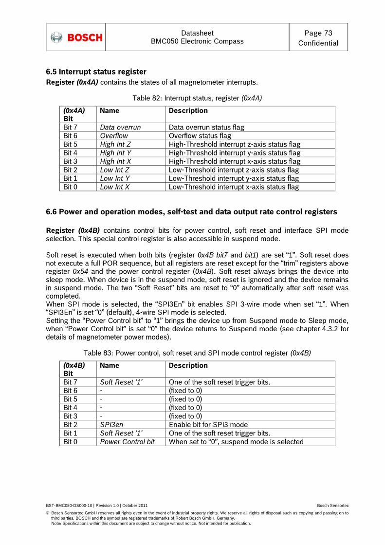
Datasheet
BMC050 Electronic Compass Page 73
Confidential
BST-BMC050-DS000-10 | Revision 1.0 | October 2011 Bosch Sensortec
© Bosch Sensortec GmbH reserves all rights even in the event of industrial property rights. We reserve all rights of disposal such as copying and passing on to
third parties. BOSCH and the symbol are registered trademarks of Robert Bosch GmbH, Germany.
Note: Specifications within this document are subject to change without notice. Not intended for publication.
6.5 Interrupt status register
Register (0x4A) contains the states of all magnetometer interrupts.
Table 82: Interrupt status, register (0x4A)
(0x4A) Bit
Name Description
Bit 7 Data overrun Data overrun status flag
Bit 6 Overflow Overflow status flag
Bit 5 High Int Z High-Threshold interrupt z-axis status flag
Bit 4 High Int Y High-Threshold interrupt y-axis status flag
Bit 3 High Int X High-Threshold interrupt x-axis status flag
Bit 2 Low Int Z Low-Threshold interrupt z-axis status flag
Bit 1 Low Int Y Low-Threshold interrupt y-axis status flag
Bit 0 Low Int X Low-Threshold interrupt x-axis status flag
6.6 Power and operation modes, self-test and data output rate control registers
Register (0x4B) contains control bits for power control, soft reset and interface SPI mode selection. This special control register is also accessible in suspend mode. Soft reset is executed when both bits (register 0x4B bit7 and bit1) are set “1”. Soft reset does not execute a full POR sequence, but all registers are reset except for the “trim” registers above register 0x54 and the power control register (0x4B). Soft reset always brings the device into sleep mode. When device is in the suspend mode, soft reset is ignored and the device remains in suspend mode. The two “Soft Reset” bits are reset to “0” automatically after soft reset was completed. When SPI mode is selected, the “SPI3En” bit enables SPI 3-wire mode when set “1”. When “SPI3En” is set “0” (default), 4-wire SPI mode is selected. Setting the “Power Control bit” to “1” brings the device up from Suspend mode to Sleep mode, when “Power Control bit” is set “0” the device returns to Suspend mode (see chapter 4.3.2 for details of magnetometer power modes).
Table 83: Power control, soft reset and SPI mode control register (0x4B)
(0x4B) Bit
Name Description
Bit 7 Soft Reset ‘1’ One of the soft reset trigger bits.
Bit 6 - (fixed to 0)
Bit 5 - (fixed to 0)
Bit 4 - (fixed to 0)
Bit 3 - (fixed to 0)
Bit 2 SPI3en Enable bit for SPI3 mode
Bit 1 Soft Reset ‘1’ One of the soft reset trigger bits.
Bit 0 Power Control bit When set to “0”, suspend mode is selected

Datasheet
BMC050 Electronic Compass Page 74
Confidential
BST-BMC050-DS000-10 | Revision 1.0 | October 2011 Bosch Sensortec
© Bosch Sensortec GmbH reserves all rights even in the event of industrial property rights. We reserve all rights of disposal such as copying and passing on to
third parties. BOSCH and the symbol are registered trademarks of Robert Bosch GmbH, Germany.
Note: Specifications within this document are subject to change without notice. Not intended for publication.
Register (0x4C) contains control bits for operation mode, output data rate and self-test. The two “Adv. ST” bits control the on-chip advanced self-test (see chapter 4.5.2 for details of the magnetometer advanced self-test). The three “Data rate” bits control the magnetometer output data rate according to below Table 85. The two “Opmode” bits control the operation mode according to below Table 86 (see chapter 4.3.2 for a detailed description of magnetometer power modes).
Table 84: Operation mode, output data rate and self-test control register (0x4C)
(0x4C) Bit
Name Description
Bit 7 Adv. ST <1> Advanced self-test control bit 1
Bit 6 Adv. ST <0> Advanced self-test control bit 0
Bit 5 Data rate <2> Data rate control bit 2
Bit 4 Data rate <1> Data rate control bit 1
Bit 3 Data rate <0> Data rate control bit 0
Bit 2 Opmode <1> Operation mode control bit 1
Bit 1 Opmode <0> Operation mode control bit 0
Bit 0 Self Test Normal self-test control bit
Three “Data rate” bits control the output data rate (ODR) of the BMC050 magnetometer part:
Table 85: Output data rate (ODR) setting (0x4C)
(0x4C) Data rate <2:0>
Magnetometer output data rate (ODR)
000b 10 (default)
001b 2
010b 6
011b 8
100b 15
101b 20
110b 25
111b 30
Two “Data rate” bits control the operation mode of the BMC050 magnetometer part:
Table 86: Operation mode setting (0x4C)
(0x4C) Opmode <1:0>
Magnetometer operation mode4
00b Normal mode
01b Forced mode
10b Reserved, do not use
11b Sleep Mode
4 See chapter 4.3.2 for a detailed description of magnetometer power modes.

Datasheet
BMC050 Electronic Compass Page 75
Confidential
BST-BMC050-DS000-10 | Revision 1.0 | October 2011 Bosch Sensortec
© Bosch Sensortec GmbH reserves all rights even in the event of industrial property rights. We reserve all rights of disposal such as copying and passing on to
third parties. BOSCH and the symbol are registered trademarks of Robert Bosch GmbH, Germany.
Note: Specifications within this document are subject to change without notice. Not intended for publication.
6.7 Interrupt and axis enable settings control registers
Register (0x4D) contains control bits for interrupt settings. (Also refer to chapter 4.9 for the details of magnetometer interrupt operation).
Table 87: Interrupt settings control register (0x4D)
(0x4D) Bit
Name Description
Bit 7 Data Overrun En Enables data overrun indication in the “Data Overrun” flag (active high, default is “0” disabled)
Bit 6 Overflow Int En Activates mapping of Overflow flag status to the INT3 pin (active high, default is “0” disabled)
Bit 5 High Int Z En Enables the z-axis detection for High-Threshold interrupts (active low, default is “1” disabled)
Bit 4 High Int Y En Enables the y-axis detection for High-Threshold interrupts (active low, default is “1” disabled)
Bit 3 High Int X En Enables the x-axis detection for High-Threshold interrupts (active low, default is “1” disabled)
Bit 2 Low Int Z En Enables the z-axis detection for Low-Threshold interrupts (active low, default is “1” disabled)
Bit 1 Low Int Y En Enables the y-axis detection for Low-Threshold interrupts (active low, default is “1” disabled)
Bit 0 Low Int X En Enables the x-axis detection for Low-Threshold interrupts (active low, default is “1” disabled)

Datasheet
BMC050 Electronic Compass Page 76
Confidential
BST-BMC050-DS000-10 | Revision 1.0 | October 2011 Bosch Sensortec
© Bosch Sensortec GmbH reserves all rights even in the event of industrial property rights. We reserve all rights of disposal such as copying and passing on to
third parties. BOSCH and the symbol are registered trademarks of Robert Bosch GmbH, Germany.
Note: Specifications within this document are subject to change without notice. Not intended for publication.
Register (0x4E) contains control bits interrupt settings and axes enable bits. (Also refer to chapter 4.9 for the details of magnetometer interrupt operation). If a magnetic measurement channel is disabled, its last measured magnetic output values will remain in the data registers. If the Z channel is disabled, the resistance measurement will also be disabled and the resistance output value will be set to zero. If interrupts are set to trigger on an axis that has been disabled, these interrupts will still be asserted based on the last measured value.
Table 88: Interrupt settings and axes enable bits control register (0x4E)
(0x4E) Bit
Name Description
Bit 7 Data Ready Pin En Enables data ready status mapping on DRDY pin (active high, default is “0” disabled)
Bit 6 Interrupt Pin En Enables interrupt status mapping on INT3 pin (active high, default is “0” disabled)
Bit 5 Channel Z Enable z-axis and resistance measurement (active low, default is “0” enabled)
Bit 4 Channel Y Enable y-axis (active low, default is “0” enabled)
Bit 3 Channel X Enable x-axis (active low, default is “0” enabled)
Bit 2 DR Polarity Data ready (DRDY) pin polarity (“0” is active low, “1” is active high, default is “1” active high)
Bit 1 Interrupt Latch Interrupt latching (“0” means non-latched - interrupt pin is on as long as the condition is fulfilled, “1” means latched - interrupt pin is on until interrupt status register 0x4A is read, default is „”1” latched)
Bit 0 Interrupt Polarity Interrupt pin INT3 polarity selection (“1” – is active high, “0” is active low, default is “1” active high)
Register (0x4F) contains the Low-Threshold interrupt threshold setting. (Also refer to chapter 4.9 for the details of magnetometer interrupt operation and the threshold setting).
Table 89: Low-threshold interrupt threshold setting control register (0x4F)
(0x4F) Bit
Name Description
Bit 7 LowThreshold <7> Bit 7 of Low-Threshold interrupt threshold setting
Bit 6 LowThreshold <6> Bit 6 of Low-Threshold interrupt threshold setting
Bit 5 LowThreshold <5> Bit 5 of Low-Threshold interrupt threshold setting
Bit 4 LowThreshold <4> Bit 4 of Low-Threshold interrupt threshold setting
Bit 3 LowThreshold <3> Bit 3 of Low-Threshold interrupt threshold setting
Bit 2 LowThreshold <2> Bit 2 of Low-Threshold interrupt threshold setting
Bit 1 LowThreshold <1> Bit 1 of Low-Threshold interrupt threshold setting
Bit 0 LowThreshold <0> Bit 0 of Low-Threshold interrupt threshold setting
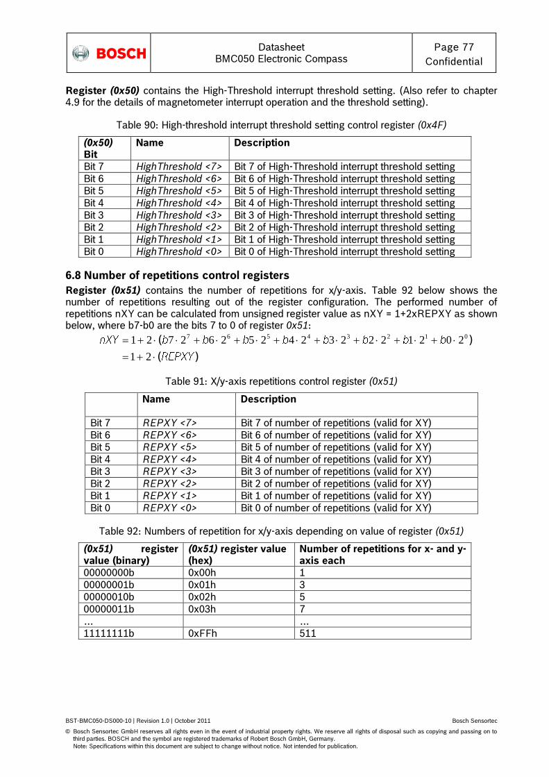
Datasheet
BMC050 Electronic Compass Page 77
Confidential
BST-BMC050-DS000-10 | Revision 1.0 | October 2011 Bosch Sensortec
© Bosch Sensortec GmbH reserves all rights even in the event of industrial property rights. We reserve all rights of disposal such as copying and passing on to
third parties. BOSCH and the symbol are registered trademarks of Robert Bosch GmbH, Germany.
Note: Specifications within this document are subject to change without notice. Not intended for publication.
Register (0x50) contains the High-Threshold interrupt threshold setting. (Also refer to chapter 4.9 for the details of magnetometer interrupt operation and the threshold setting).
Table 90: High-threshold interrupt threshold setting control register (0x4F)
(0x50) Bit
Name Description
Bit 7 HighThreshold <7> Bit 7 of High-Threshold interrupt threshold setting
Bit 6 HighThreshold <6> Bit 6 of High-Threshold interrupt threshold setting
Bit 5 HighThreshold <5> Bit 5 of High-Threshold interrupt threshold setting
Bit 4 HighThreshold <4> Bit 4 of High-Threshold interrupt threshold setting
Bit 3 HighThreshold <3> Bit 3 of High-Threshold interrupt threshold setting
Bit 2 HighThreshold <2> Bit 2 of High-Threshold interrupt threshold setting
Bit 1 HighThreshold <1> Bit 1 of High-Threshold interrupt threshold setting
Bit 0 HighThreshold <0> Bit 0 of High-Threshold interrupt threshold setting
6.8 Number of repetitions control registers
Register (0x51) contains the number of repetitions for x/y-axis. Table 92 below shows the number of repetitions resulting out of the register configuration. The performed number of repetitions nXY can be calculated from unsigned register value as nXY = 1+2xREPXY as shown below, where b7-b0 are the bits 7 to 0 of register 0x51:
)(
)(
21
202122232425262721 01234567
Table 91: X/y-axis repetitions control register (0x51)
Name Description
Bit 7 REPXY <7> Bit 7 of number of repetitions (valid for XY)
Bit 6 REPXY <6> Bit 6 of number of repetitions (valid for XY)
Bit 5 REPXY <5> Bit 5 of number of repetitions (valid for XY)
Bit 4 REPXY <4> Bit 4 of number of repetitions (valid for XY)
Bit 3 REPXY <3> Bit 3 of number of repetitions (valid for XY)
Bit 2 REPXY <2> Bit 2 of number of repetitions (valid for XY)
Bit 1 REPXY <1> Bit 1 of number of repetitions (valid for XY)
Bit 0 REPXY <0> Bit 0 of number of repetitions (valid for XY)
Table 92: Numbers of repetition for x/y-axis depending on value of register (0x51)
(0x51) register value (binary)
(0x51) register value (hex)
Number of repetitions for x- and y-axis each
00000000b 0x00h 1
00000001b 0x01h 3
00000010b 0x02h 5
00000011b 0x03h 7
… …
11111111b 0xFFh 511

Datasheet
BMC050 Electronic Compass Page 78
Confidential
BST-BMC050-DS000-10 | Revision 1.0 | October 2011 Bosch Sensortec
© Bosch Sensortec GmbH reserves all rights even in the event of industrial property rights. We reserve all rights of disposal such as copying and passing on to
third parties. BOSCH and the symbol are registered trademarks of Robert Bosch GmbH, Germany.
Note: Specifications within this document are subject to change without notice. Not intended for publication.
Register (0x52) contains the number of repetitions for z-axis. Table 94 below shows the number of repetitions resulting out of the register configuration. The performed number of repetitions nZ can be calculated from unsigned register value as nZ = 1+REPZ as shown below, where b7-b0 are the bits 7 to 0 of register 0x52:
1
202122232425262711 01234567 )(
Table 93: Z-axis repetitions control register (0x52)
(0x52) Bit
Name Description
Bit 7 REPZ <7> Bit 7 of number of repetitions (valid for Z)
Bit 6 REPZ <6> Bit 6 of number of repetitions (valid for Z)
Bit 5 REPZ <5> Bit 5 of number of repetitions (valid for Z)
Bit 4 REPZ <4> Bit 4 of number of repetitions (valid for Z)
Bit 3 REPZ <3> Bit 3 of number of repetitions (valid for Z)
Bit 2 REPZ <2> Bit 2 of number of repetitions (valid for Z)
Bit 1 REPZ <1> Bit 1 of number of repetitions (valid for Z)
Bit 0 REPZ <0> Bit 0 of number of repetitions (valid for Z)
Table 94: Numbers of repetition for z-axis depending on value of register (0x52)
(0x52) register value (binary)
(0x52) register value (hex)
Number of repetitions for z-axis
00000000b 0x00h 1
00000001b 0x01h 2
00000010b 0x02h 3
00000011b 0x03h 4
… …
11111111b 0xFFh 256
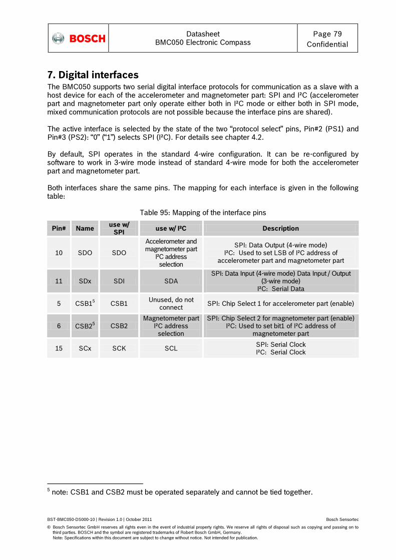
Datasheet
BMC050 Electronic Compass Page 79
Confidential
BST-BMC050-DS000-10 | Revision 1.0 | October 2011 Bosch Sensortec
© Bosch Sensortec GmbH reserves all rights even in the event of industrial property rights. We reserve all rights of disposal such as copying and passing on to
third parties. BOSCH and the symbol are registered trademarks of Robert Bosch GmbH, Germany.
Note: Specifications within this document are subject to change without notice. Not intended for publication.
7. Digital interfaces The BMC050 supports two serial digital interface protocols for communication as a slave with a host device for each of the accelerometer and magnetometer part: SPI and I²C (accelerometer part and magnetometer part only operate either both in I²C mode or either both in SPI mode, mixed communication protocols are not possible because the interface pins are shared). The active interface is selected by the state of the two “protocol select” pins, Pin#2 (PS1) and Pin#3 (PS2): “0” (“1”) selects SPI (I²C). For details see chapter 4.2. By default, SPI operates in the standard 4-wire configuration. It can be re-configured by software to work in 3-wire mode instead of standard 4-wire mode for both the accelerometer part and magnetometer part. Both interfaces share the same pins. The mapping for each interface is given in the following table:
Table 95: Mapping of the interface pins
Pin# Name use w/
SPI use w/ I²C Description
10 SDO SDO
Accelerometer and magnetometer part
I²C address selection
SPI: Data Output (4-wire mode) I²C: Used to set LSB of I²C address of
accelerometer part and magnetometer part
11 SDx SDI SDA SPI: Data Input (4-wire mode) Data Input / Output
(3-wire mode) I²C: Serial Data
5 CSB15 CSB1
Unused, do not connect
SPI: Chip Select 1 for accelerometer part (enable)
6 CSB25 CSB2
Magnetometer part I²C address
selection
SPI: Chip Select 2 for magnetometer part (enable) I²C: Used to set bit1 of I²C address of
magnetometer part
15 SCx SCK SCL SPI: Serial Clock I²C: Serial Clock
5 note: CSB1 and CSB2 must be operated separately and cannot be tied together.
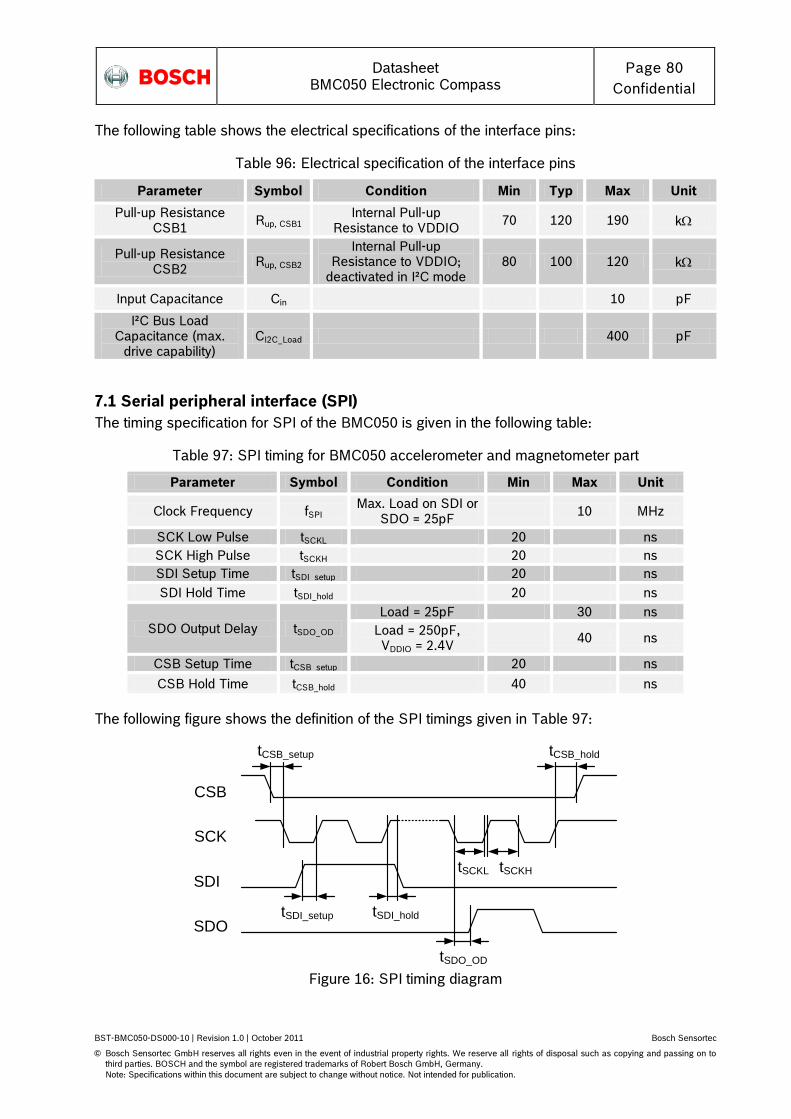
Datasheet
BMC050 Electronic Compass Page 80
Confidential
BST-BMC050-DS000-10 | Revision 1.0 | October 2011 Bosch Sensortec
© Bosch Sensortec GmbH reserves all rights even in the event of industrial property rights. We reserve all rights of disposal such as copying and passing on to
third parties. BOSCH and the symbol are registered trademarks of Robert Bosch GmbH, Germany.
Note: Specifications within this document are subject to change without notice. Not intended for publication.
The following table shows the electrical specifications of the interface pins:
Table 96: Electrical specification of the interface pins
Parameter Symbol Condition Min Typ Max Unit
Pull-up Resistance CSB1
Rup, CSB1 Internal Pull-up
Resistance to VDDIO 70 120 190 k
Pull-up Resistance CSB2
Rup, CSB2 Internal Pull-up
Resistance to VDDIO; deactivated in I²C mode
80 100 120 k
Input Capacitance Cin 10 pF
I²C Bus Load Capacitance (max.
drive capability) CI2C_Load 400 pF
7.1 Serial peripheral interface (SPI)
The timing specification for SPI of the BMC050 is given in the following table:
Table 97: SPI timing for BMC050 accelerometer and magnetometer part
Parameter Symbol Condition Min Max Unit
Clock Frequency fSPI Max. Load on SDI or
SDO = 25pF 10 MHz
SCK Low Pulse tSCKL 20 ns
SCK High Pulse tSCKH 20 ns
SDI Setup Time tSDI_setup 20 ns
SDI Hold Time tSDI_hold 20 ns
SDO Output Delay tSDO_OD
Load = 25pF 30 ns
Load = 250pF, VDDIO = 2.4V
40 ns
CSB Setup Time tCSB_setup 20 ns
CSB Hold Time tCSB_hold 40 ns
The following figure shows the definition of the SPI timings given in Table 97:
Figure 16: SPI timing diagram
tSDI_hold
tSCKH
tCSB_holdtCSB_setup
tSDI_setup
tSCKL
tSDO_OD
CSB
SCK
SDI
SDO

Datasheet
BMC050 Electronic Compass Page 81
Confidential
BST-BMC050-DS000-10 | Revision 1.0 | October 2011 Bosch Sensortec
© Bosch Sensortec GmbH reserves all rights even in the event of industrial property rights. We reserve all rights of disposal such as copying and passing on to
third parties. BOSCH and the symbol are registered trademarks of Robert Bosch GmbH, Germany.
Note: Specifications within this document are subject to change without notice. Not intended for publication.
The SPI interface of the BMC050 is compatible with two modes, “00” and “11”. The automatic selection between [CPOL = “0” and CPHA = “0”] and [CPOL = “1” and CPHA = “1”] is done based on the value of SCK after a falling edge of CSB. Two configurations of the SPI interface are supported by the BMC050: 4-wire and 3-wire. The same protocol is used by both configurations. The device operates in 4-wire configuration by default. It can be switched to 3-wire configuration by writing “1” to (0x34) “spi3” for the accelerometer part and writing “1” to (0x4B) “SPI3en” for the magnetometer part (after power control bit was set). Pin SDI is used as the common data pin in 3-wire configuration. For single byte read as well as write operations, 16-bit protocols are used. The BMC050 also supports multiple-byte read operations. Note: CSB1 and CSB2 pin are separate chip select lines for accelerometer and magnetometer part, which must be operated separately. Tying them together is strictly forbidden, since this will make the accelerometer and magnetometer outputs compete against each other. In SPI 4-wire configuration CSB1 or CSB2 (chip select low active), SCK (serial clock), SDI (serial data input), and SDO (serial data output) pins are used. The communication starts when the CSB is pulled low by the SPI master and stops when CSB is pulled high. SCK is also controlled by SPI master. SDI and SDO are driven at the falling edge of SCK and should be captured at the rising edge of SCK. The basic write operation waveform for 4-wire configuration is depicted in Figure 17. During the entire write cycle SDO remains in high- impedance state.
CSB
SCK
SDI
R/W AD6 AD5 AD4 AD3 AD2 AD1 AD0 DI5 DI4 DI3 DI2 DI1 DI0 DI7 DI6
SDO
tri-state
Z
Figure 17: 4-wire basic SPI write sequence (mode “11”)
The basic read operation waveform for 4-wire configuration is depicted in Figure 18:
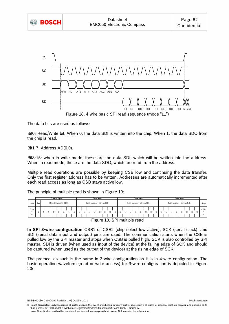
Datasheet
BMC050 Electronic Compass Page 82
Confidential
BST-BMC050-DS000-10 | Revision 1.0 | October 2011 Bosch Sensortec
© Bosch Sensortec GmbH reserves all rights even in the event of industrial property rights. We reserve all rights of disposal such as copying and passing on to
third parties. BOSCH and the symbol are registered trademarks of Robert Bosch GmbH, Germany.
Note: Specifications within this document are subject to change without notice. Not intended for publication.
Figure 18: 4-wire basic SPI read sequence (mode “11”)
The data bits are used as follows: Bit0: Read/Write bit. When 0, the data SDI is written into the chip. When 1, the data SDO from the chip is read. Bit1-7: Address AD(6:0). Bit8-15: when in write mode, these are the data SDI, which will be written into the address. When in read mode, these are the data SDO, which are read from the address. Multiple read operations are possible by keeping CSB low and continuing the data transfer. Only the first register address has to be written. Addresses are automatically incremented after each read access as long as CSB stays active low. The principle of multiple read is shown in Figure 19:
Figure 19: SPI multiple read
In SPI 3-wire configuration CSB1 or CSB2 (chip select low active), SCK (serial clock), and SDI (serial data input and output) pins are used. The communication starts when the CSB is pulled low by the SPI master and stops when CSB is pulled high. SCK is also controlled by SPI master. SDI is driven (when used as input of the device) at the falling edge of SCK and should be captured (when used as the output of the device) at the rising edge of SCK. The protocol as such is the same in 3-wire configuration as it is in 4-wire configuration. The basic operation waveform (read or write access) for 3-wire configuration is depicted in Figure 20:
Start RW Stop
1 0 0 0 0 0 1 0 X X X X X X X X X X X X X X X X X X X X X X X X
Register adress (02h)
CSB
=
0
CSB
=
1
Data byte Data byte
Data register - adress 03h Data register - adress 04h
Control byte Data byte
Data register - adress 02h
CSB
SCK
SDI
R/W AD
6 AD
5 A
D 4 A
D 3 AD 2
AD1 AD
0
SDO
DO5 DO
4 DO3 DO
2 DO1 DO
0 DO7 DO
6 tri
- state
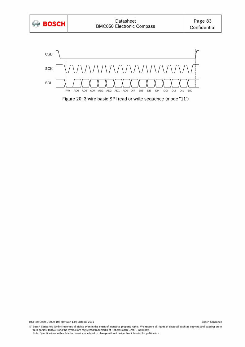
Datasheet
BMC050 Electronic Compass Page 83
Confidential
BST-BMC050-DS000-10 | Revision 1.0 | October 2011 Bosch Sensortec
© Bosch Sensortec GmbH reserves all rights even in the event of industrial property rights. We reserve all rights of disposal such as copying and passing on to
third parties. BOSCH and the symbol are registered trademarks of Robert Bosch GmbH, Germany.
Note: Specifications within this document are subject to change without notice. Not intended for publication.
CSB
SCK
SDI
RW AD6 AD5 AD4 AD3 AD2 AD1 AD0 DI5 DI4 DI3 DI2 DI1 DI0 DI7 DI6
Figure 20: 3-wire basic SPI read or write sequence (mode “11”)

Datasheet
BMC050 Electronic Compass Page 84
Confidential
BST-BMC050-DS000-10 | Revision 1.0 | October 2011 Bosch Sensortec
© Bosch Sensortec GmbH reserves all rights even in the event of industrial property rights. We reserve all rights of disposal such as copying and passing on to
third parties. BOSCH and the symbol are registered trademarks of Robert Bosch GmbH, Germany.
Note: Specifications within this document are subject to change without notice. Not intended for publication.
7.2 Inter-Integrated Circuit (I²C)
The I²C bus uses SCL (= SCx pin, serial clock) and SDA (= SDx pin, serial data input and output) signal lines. Both lines are connected to VDDIO externally via pull-up resistors so that they are pulled high when the bus is free. The I²C interface of the BMC050 is compatible with the I²C Specification UM10204 Rev. 03 (19 June 2007), available at http://www.nxp.com. The BMC050 supports I²C standard mode and fast mode, only 7-bit address mode is supported. The default I²C address of the BMC050‟s accelerometer part is 0011000b (0x18). It is used if the SDO pin is pulled to “GND”. The alternative address 0011001b (0x19) is selected by pulling the SDO pin to “VDDIO”. The default I²C address of the BMC050‟s magnetometer part is 0x10. The five MSB are hardwired to “00100”. In order to prevent bus conflicts bit0 can be inverted by setting „1‟ to SDO, and the bit 1 can be inverted by setting „1‟ to the CSB line according to below Table:
Table 98: BMC050 I²C addresses
CSB2 pin SDO pin Accelerometer
part I²C address Magnetometer part I²C
address
GND GND 0x18 0x10
GND VDDIO 0x19 0x11
VDDIO GND 0x18 0x12
VDDIO VDDIO 0x19 0x13 The timing specification for I²C of the BMC050 is given in Table 99:
Table 99: I²C timings.
Parameter Symbol Condition Min Max Unit
Clock Frequency fSCL 400 kHz
SCL Low Period tLOW 6 6
s
SCL High Period tHIGH 6 6
SDA Setup Time tSUDAT 6 6
SDA Hold Time tHDDAT 6 6
Setup Time for a repeated Start
Condition tSUSTA 6 6
Hold Time for a Start Condition
tHDSTA 6 6
Setup Time for a Stop Condition
tSUSTO 6 6
Time before a new Transmission can
start tBUF 6 6
6 fully compliant to the I2C specification”UM10204 I2C-bus specification Rev.03 – 19 June 2007”
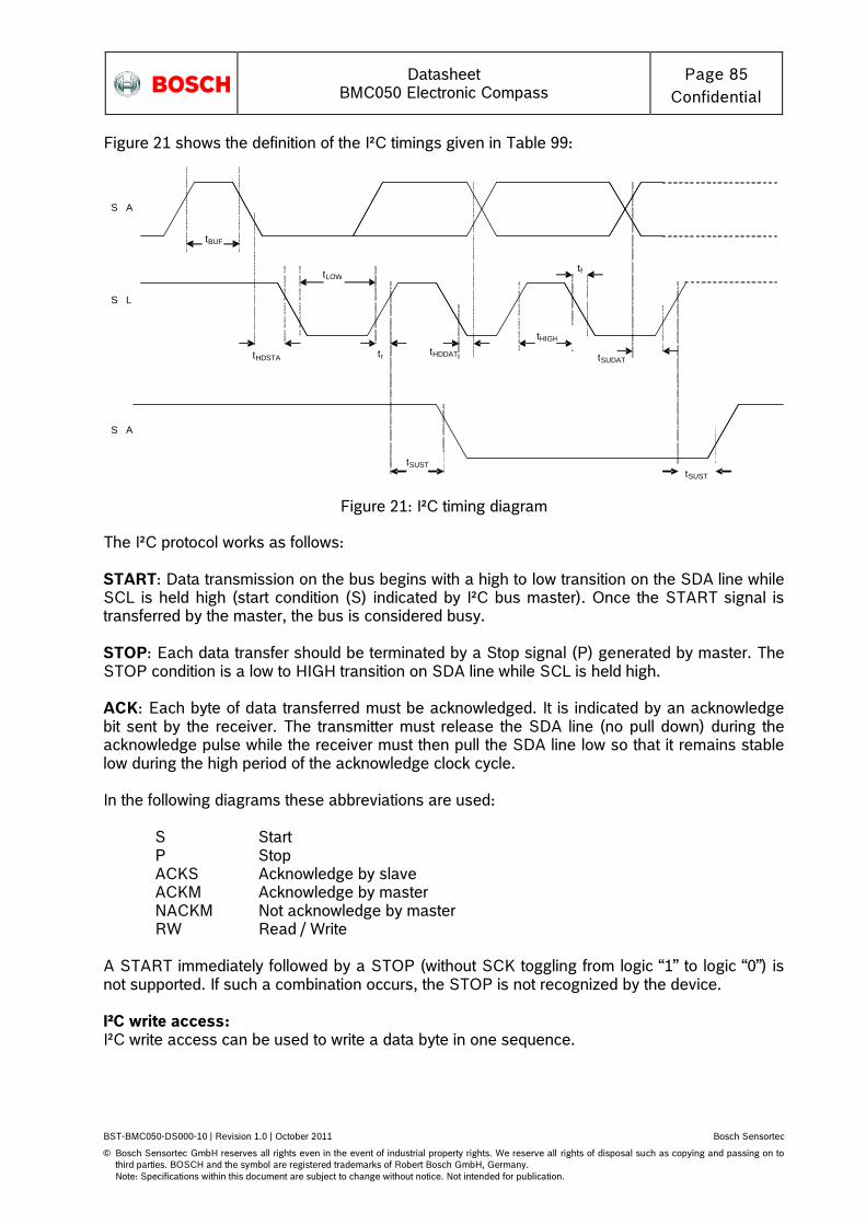
Datasheet
BMC050 Electronic Compass Page 85
Confidential
BST-BMC050-DS000-10 | Revision 1.0 | October 2011 Bosch Sensortec
© Bosch Sensortec GmbH reserves all rights even in the event of industrial property rights. We reserve all rights of disposal such as copying and passing on to
third parties. BOSCH and the symbol are registered trademarks of Robert Bosch GmbH, Germany.
Note: Specifications within this document are subject to change without notice. Not intended for publication.
Figure 21 shows the definition of the I²C timings given in Table 99:
Figure 21: I²C timing diagram
The I²C protocol works as follows: START: Data transmission on the bus begins with a high to low transition on the SDA line while SCL is held high (start condition (S) indicated by I²C bus master). Once the START signal is transferred by the master, the bus is considered busy. STOP: Each data transfer should be terminated by a Stop signal (P) generated by master. The STOP condition is a low to HIGH transition on SDA line while SCL is held high. ACK: Each byte of data transferred must be acknowledged. It is indicated by an acknowledge bit sent by the receiver. The transmitter must release the SDA line (no pull down) during the acknowledge pulse while the receiver must then pull the SDA line low so that it remains stable low during the high period of the acknowledge clock cycle. In the following diagrams these abbreviations are used: S Start P Stop ACKS Acknowledge by slave ACKM Acknowledge by master NACKM Not acknowledge by master RW Read / Write A START immediately followed by a STOP (without SCK toggling from logic “1” to logic “0”) is not supported. If such a combination occurs, the STOP is not recognized by the device. I²C write access: I²C write access can be used to write a data byte in one sequence.
t HDDAT
t f
t BUF
SD
A
SC
L
SD
A
t LOW
t HDSTA t r
t SUSTA
t HIGH t SUDAT
t SUSTO

Datasheet
BMC050 Electronic Compass Page 86
Confidential
BST-BMC050-DS000-10 | Revision 1.0 | October 2011 Bosch Sensortec
© Bosch Sensortec GmbH reserves all rights even in the event of industrial property rights. We reserve all rights of disposal such as copying and passing on to
third parties. BOSCH and the symbol are registered trademarks of Robert Bosch GmbH, Germany.
Note: Specifications within this document are subject to change without notice. Not intended for publication.
The sequence begins with start condition generated by the master, followed by 7 bits slave address and a write bit (RW = 0). The slave sends an acknowledge bit (ACK = 0) and releases the bus. Then the master sends the one byte register address. The slave again acknowledges the transmission and waits for the 8 bits of data which shall be written to the specified register address. After the slave acknowledges the data byte, the master generates a stop signal and terminates the writing protocol. Example of an I²C write access:
Figure 22: Example of an I²C write access
I²C read access: I²C read access also can be used to read one or multiple data bytes in one sequence. A read sequence consists of a one-byte I²C write phase followed by the I²C read phase. The two parts of the transmission must be separated by a repeated start condition (Sr). The I²C write phase addresses the slave and sends the register address to be read. After slave acknowledges the transmission, the master generates again a start condition and sends the slave address together with a read bit (RW = 1). Then the master releases the bus and waits for the data bytes to be read out from slave. After each data byte the master has to generate an acknowledge bit (ACK = 0) to enable further data transfer. A NACKM (ACK = 1) from the master stops the data being transferred from the slave. The slave releases the bus so that the master can generate a STOP condition and terminate the transmission. The register address is automatically incremented and, therefore, more than one byte can be sequentially read out. Once a new data read transmission starts, the start address will be set to the register address specified in the latest I²C write command. By default the start address is set at 0x00. In this way repetitive multi-bytes reads from the same starting address are possible. In order to prevent the I²C slave of the device to lock-up the I²C bus, a watchdog timer (WDT) is implemented in the accelerometer part of BMC050. The WDT observes internal I²C signals and resets the I²C interface if the bus is locked-up by the BMC050 accelerometer part. The activity and the timer period of the WDT can be configured through the bits (0x34) i2c_wdt_en and (0x34) i2c_wdt_sel. Writing “1” (“0”) to (0x34) i2c_wdt_en activates (de-activates) the WDT. Writing “0” (“1”) to (0x34) i2c_wdt_se selects a timer period of 1 ms (50 ms). Example of an I²C multiple read accesses:
Start RW ACKS ACKS ACKS Stop
0 0 1 1 0 0 0 0 0 0 0 1 0 0 0 0 X X X X X X X XS
Slave Adress Register adress (0x10)
Control byte Data byte
Data (0x09)
P

Datasheet
BMC050 Electronic Compass Page 87
Confidential
BST-BMC050-DS000-10 | Revision 1.0 | October 2011 Bosch Sensortec
© Bosch Sensortec GmbH reserves all rights even in the event of industrial property rights. We reserve all rights of disposal such as copying and passing on to
third parties. BOSCH and the symbol are registered trademarks of Robert Bosch GmbH, Germany.
Note: Specifications within this document are subject to change without notice. Not intended for publication.
Figure 23: Example of an I²C multiple read access
Start RW ACKS
dum
my
ACKS Stop
0 0 1 1 0 0 0 0 X 0 0 0 0 0 1 0
Start RW ACKS ACKM ACKM
0 0 1 1 0 0 0 1 X X X X X X X X X X X X X X X X …
ACKM ACKM
… X X X X X X X X X X X X X X X X …
ACKM NACK Stop
… X X X X X X X X X X X X X X X X
Data byte Data byte
Read Data (0x04) Read Data (0x05)
P
Data byte Data byte
Read Data (0x06) Read Data (0x07)
S
Slave Adress Register adress (0x02)
Slave Adress Read Data (0x03)Read Data (0x02)
Control byte
P
Data byte Data byte
Sr

Datasheet
BMC050 Electronic Compass Page 88
Confidential
BST-BMC050-DS000-10 | Revision 1.0 | October 2011 Bosch Sensortec
© Bosch Sensortec GmbH reserves all rights even in the event of industrial property rights. We reserve all rights of disposal such as copying and passing on to
third parties. BOSCH and the symbol are registered trademarks of Robert Bosch GmbH, Germany.
Note: Specifications within this document are subject to change without notice. Not intended for publication.
8. Pin-out and connection diagram
8.1 Pin-out
Figure 24: Pin-out top view Figure 25: Pin-out bottom view
The arrows indicate the pin1 marking.
TOP VIEW
(pads not visible)
141516 13 12
87654
1
3
2
11
9
10BOTTOM VIEW
(pads visible)
14 15 161312
8 7 6 5 4
1
3
2
11
9
10a

Datasheet
BMC050 Electronic Compass Page 89
Confidential
BST-BMC050-DS000-10 | Revision 1.0 | October 2011 Bosch Sensortec
© Bosch Sensortec GmbH reserves all rights even in the event of industrial property rights. We reserve all rights of disposal such as copying and passing on to
third parties. BOSCH and the symbol are registered trademarks of Robert Bosch GmbH, Germany.
Note: Specifications within this document are subject to change without notice. Not intended for publication.
Table 100: Pin description
Pin Name I/O Type Sensor Description Connect to
SPI 4W SPI 3W I²C
1 INT2 Out Acc Interrupt output #2 INT2 input or DNC if unused
2 PS1 In Acc Protocol select #1 GND GND VDDIO
3 PS2 In Mag Protocol select #2 GND GND VDDIO
4 INT3 Out Mag Interrupt output #3 INT3 input or DNC if unused
5 CSB17 In Acc Chip Select #1 CSB1 CSB1
NC (float) or VDDIO
6 CSB27 In Mag Chip Select #2 CSB2 CSB2
GND for default
address
7 GND Supply Mag+Ac
c Ground GND
8 GND Supply Mag+Ac
c Ground GND
9 DRDY Out Mag Data ready DRDY input or DNC if unused
10 SDO Out Mag+Ac
c SPI: Data out
SDO / MISO
DNC (float)
GND for default
address
11 SDI In/Out Mag+Ac
c SPI: Data in, I²C:
Data SDI / MOSI SDA SDA
12 GND Supply Mag+Ac
c Ground GND
13 VDD Supply Mag+Ac
c Supply voltage VDD
14 VDDIO Supply Mag+Ac
c I/O voltage VDDIO
15 SCK In Mag+Ac
c Serial clock SCK SCK SCL
16 INT1 Out Acc Interrupt output #1 INT 1 input or DNC if unused
7 Note: CSB1 and CSB2 must be operated separately and cannot be tied together.

Datasheet
BMC050 Electronic Compass Page 90
Confidential
BST-BMC050-DS000-10 | Revision 1.0 | October 2011 Bosch Sensortec
© Bosch Sensortec GmbH reserves all rights even in the event of industrial property rights. We reserve all rights of disposal such as copying and passing on to
third parties. BOSCH and the symbol are registered trademarks of Robert Bosch GmbH, Germany.
Note: Specifications within this document are subject to change without notice. Not intended for publication.
8.2 Connection diagram 4-wire SPI
Figure 26: 4-wire SPI connection diagram
Note: the recommended value for C1, C2 is 100 nF. CSB1 and CSB2 must be operated separately.
TOP VIEW
(pads not visible)
141516 13 12
87654
1
3
2
11
9
10PS1
PS2
INT2
INT
3
CS
B1
CS
B2
DRDY
SDO
SDI
C1C2SC
K
INT
1
VDDIO VDD
VDDIO VDD

Datasheet
BMC050 Electronic Compass Page 91
Confidential
BST-BMC050-DS000-10 | Revision 1.0 | October 2011 Bosch Sensortec
© Bosch Sensortec GmbH reserves all rights even in the event of industrial property rights. We reserve all rights of disposal such as copying and passing on to
third parties. BOSCH and the symbol are registered trademarks of Robert Bosch GmbH, Germany.
Note: Specifications within this document are subject to change without notice. Not intended for publication.
8.3 Connection diagram 3-wire SPI
Figure 27: 3-wire SPI connection diagram
Note: the recommended value for C1, C2 is 100 nF. CSB1 and CSB2 must be operated separately.
TOP VIEW
(pads not visible)
141516 13 12
87654
1
3
2
11
9
10PS1
PS2
INT2
INT
3
CS
B1
CS
B2
DRDY
SDI
C1C2SC
K
INT
1
VDDIO VDD
VDDIO VDD

Datasheet
BMC050 Electronic Compass Page 92
Confidential
BST-BMC050-DS000-10 | Revision 1.0 | October 2011 Bosch Sensortec
© Bosch Sensortec GmbH reserves all rights even in the event of industrial property rights. We reserve all rights of disposal such as copying and passing on to
third parties. BOSCH and the symbol are registered trademarks of Robert Bosch GmbH, Germany.
Note: Specifications within this document are subject to change without notice. Not intended for publication.
8.4 Connection diagram I2C
Figure 28: I²C connection diagram
Note: the recommended value for C1, C2 is 100 nF.
TOP VIEW
(pads not visible)
141516 13 12
87654
1
3
2
11
9
10PS1
PS2
INT2
INT
3
SDA
C1C2SC
K
INT
1
DRDY
VDDIO VDD
VDDIO
SDOmag & accel
address bit 0
default
mag & accel
address bit 0
inverted
VDDIO
magnetic
address bit 1
default
magnetic
address bit 1
inverted
CSB2
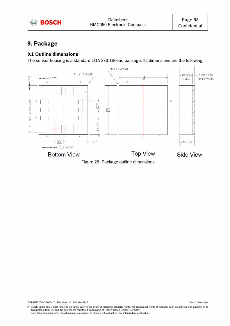
Datasheet
BMC050 Electronic Compass Page 93
Confidential
BST-BMC050-DS000-10 | Revision 1.0 | October 2011 Bosch Sensortec
© Bosch Sensortec GmbH reserves all rights even in the event of industrial property rights. We reserve all rights of disposal such as copying and passing on to
third parties. BOSCH and the symbol are registered trademarks of Robert Bosch GmbH, Germany.
Note: Specifications within this document are subject to change without notice. Not intended for publication.
9. Package
9.1 Outline dimensions
The sensor housing is a standard LGA 3x3 16-lead package. Its dimensions are the following:
Figure 29: Package outline dimensions
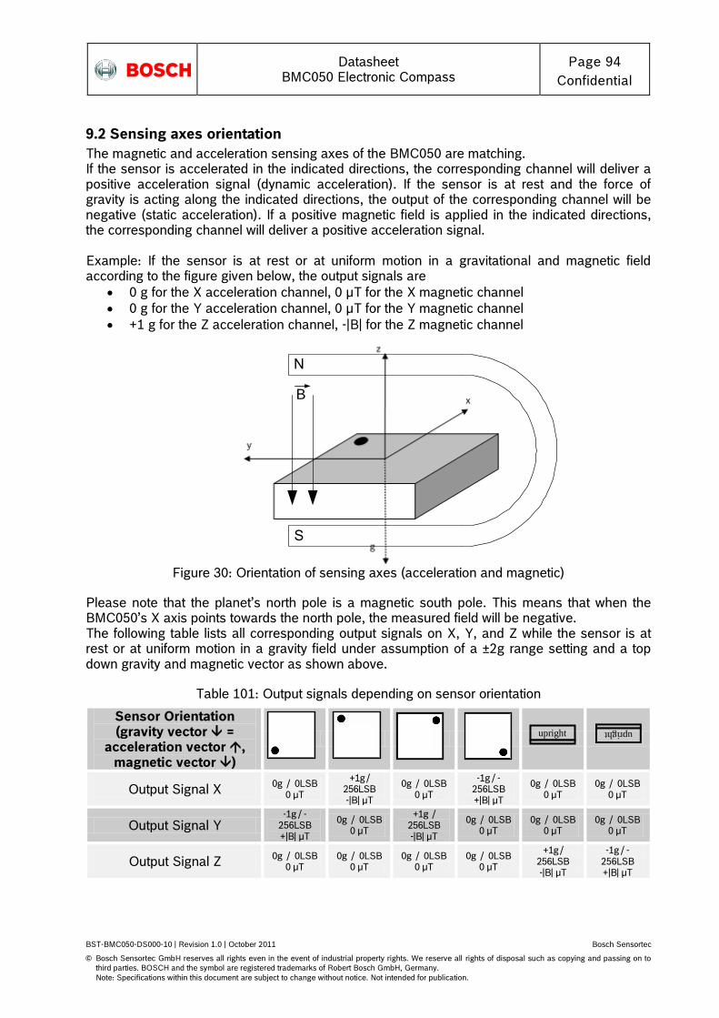
Datasheet
BMC050 Electronic Compass Page 94
Confidential
BST-BMC050-DS000-10 | Revision 1.0 | October 2011 Bosch Sensortec
© Bosch Sensortec GmbH reserves all rights even in the event of industrial property rights. We reserve all rights of disposal such as copying and passing on to
third parties. BOSCH and the symbol are registered trademarks of Robert Bosch GmbH, Germany.
Note: Specifications within this document are subject to change without notice. Not intended for publication.
9.2 Sensing axes orientation
The magnetic and acceleration sensing axes of the BMC050 are matching. If the sensor is accelerated in the indicated directions, the corresponding channel will deliver a positive acceleration signal (dynamic acceleration). If the sensor is at rest and the force of gravity is acting along the indicated directions, the output of the corresponding channel will be negative (static acceleration). If a positive magnetic field is applied in the indicated directions, the corresponding channel will deliver a positive acceleration signal. Example: If the sensor is at rest or at uniform motion in a gravitational and magnetic field according to the figure given below, the output signals are
0 g for the X acceleration channel, 0 µT for the X magnetic channel
0 g for the Y acceleration channel, 0 µT for the Y magnetic channel
+1 g for the Z acceleration channel, -|B| for the Z magnetic channel
Figure 30: Orientation of sensing axes (acceleration and magnetic)
Please note that the planet‟s north pole is a magnetic south pole. This means that when the BMC050‟s X axis points towards the north pole, the measured field will be negative. The following table lists all corresponding output signals on X, Y, and Z while the sensor is at rest or at uniform motion in a gravity field under assumption of a ±2g range setting and a top down gravity and magnetic vector as shown above.
Table 101: Output signals depending on sensor orientation
Sensor Orientation (gravity vector =
acceleration vector , magnetic vector )
Output Signal X 0g / 0LSB
0 µT
+1g / 256LSB -|B| µT
0g / 0LSB 0 µT
-1g / -256LSB +|B| µT
0g / 0LSB 0 µT
0g / 0LSB 0 µT
Output Signal Y -1g / -
256LSB +|B| µT
0g / 0LSB 0 µT
+1g / 256LSB -|B| µT
0g / 0LSB 0 µT
0g / 0LSB 0 µT
0g / 0LSB 0 µT
Output Signal Z 0g / 0LSB
0 µT 0g / 0LSB
0 µT 0g / 0LSB
0 µT 0g / 0LSB
0 µT
+1g / 256LSB -|B| µT
-1g / -256LSB +|B| µT
upright
upright
N
S
B
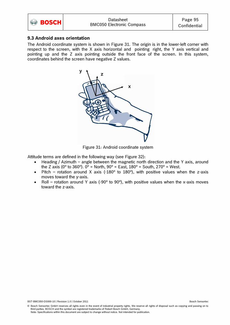
Datasheet
BMC050 Electronic Compass Page 95
Confidential
BST-BMC050-DS000-10 | Revision 1.0 | October 2011 Bosch Sensortec
© Bosch Sensortec GmbH reserves all rights even in the event of industrial property rights. We reserve all rights of disposal such as copying and passing on to
third parties. BOSCH and the symbol are registered trademarks of Robert Bosch GmbH, Germany.
Note: Specifications within this document are subject to change without notice. Not intended for publication.
9.3 Android axes orientation
The Android coordinate system is shown in Figure 31. The origin is in the lower-left corner with respect to the screen, with the X axis horizontal and pointing right, the Y axis vertical and pointing up and the Z axis pointing outside the front face of the screen. In this system, coordinates behind the screen have negative Z values.
Figure 31: Android coordinate system
Attitude terms are defined in the following way (see Figure 32):
Heading / Azimuth – angle between the magnetic north direction and the Y axis, around the Z axis (0° to 360°). 0° = North, 90° = East, 180° = South, 270° = West.
Pitch – rotation around X axis (-180° to 180°), with positive values when the z-axis moves toward the y-axis.
Roll – rotation around Y axis (-90° to 90°), with positive values when the x-axis moves toward the z-axis.

Datasheet
BMC050 Electronic Compass Page 96
Confidential
BST-BMC050-DS000-10 | Revision 1.0 | October 2011 Bosch Sensortec
© Bosch Sensortec GmbH reserves all rights even in the event of industrial property rights. We reserve all rights of disposal such as copying and passing on to
third parties. BOSCH and the symbol are registered trademarks of Robert Bosch GmbH, Germany.
Note: Specifications within this document are subject to change without notice. Not intended for publication.
Figure 32: Heading, pitch and roll in Android coordinate frame
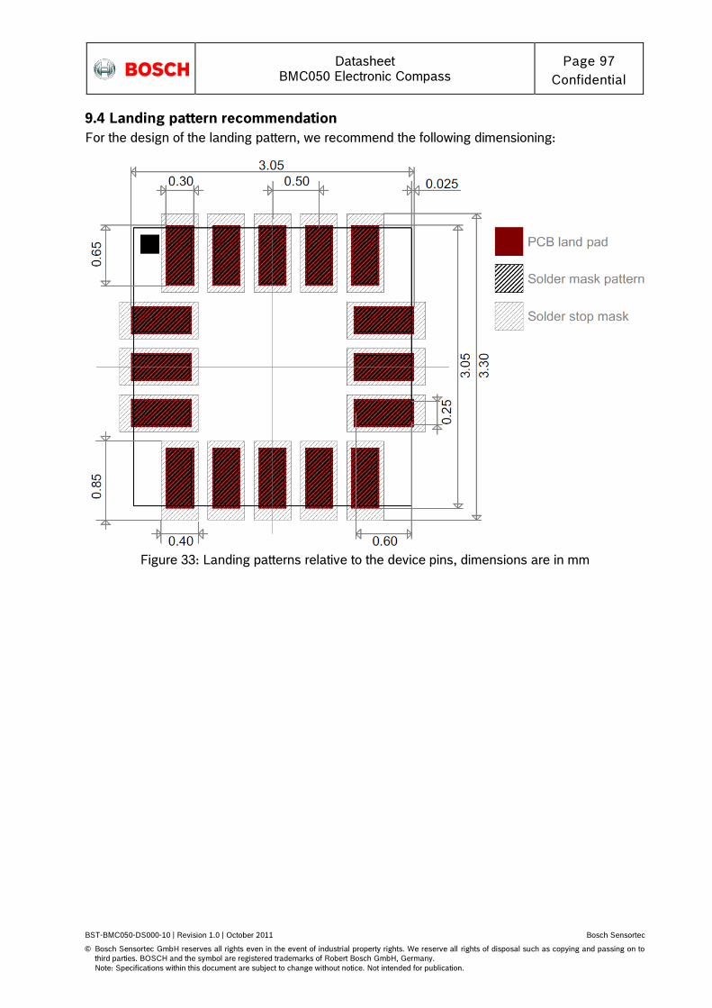
Datasheet
BMC050 Electronic Compass Page 97
Confidential
BST-BMC050-DS000-10 | Revision 1.0 | October 2011 Bosch Sensortec
© Bosch Sensortec GmbH reserves all rights even in the event of industrial property rights. We reserve all rights of disposal such as copying and passing on to
third parties. BOSCH and the symbol are registered trademarks of Robert Bosch GmbH, Germany.
Note: Specifications within this document are subject to change without notice. Not intended for publication.
9.4 Landing pattern recommendation
For the design of the landing pattern, we recommend the following dimensioning:
Figure 33: Landing patterns relative to the device pins, dimensions are in mm

Datasheet
BMC050 Electronic Compass Page 98
Confidential
BST-BMC050-DS000-10 | Revision 1.0 | October 2011 Bosch Sensortec
© Bosch Sensortec GmbH reserves all rights even in the event of industrial property rights. We reserve all rights of disposal such as copying and passing on to
third parties. BOSCH and the symbol are registered trademarks of Robert Bosch GmbH, Germany.
Note: Specifications within this document are subject to change without notice. Not intended for publication.
9.5 Marking
9.5.1 Mass production devices
Table 102: Marking of mass production samples
Labeling Name Symbol Remark
Product number 124
Sub-Con ID A Packaging sub-contractor identifier,
coded alphanumerically
Date code YWW Y: year, numerically coded:
9 = 2009, 0 = 2010, 1 = 2011, ... WW: Calendar week, numerical code
Lot counter CCC Numerical counter
Pin 1 identifier
9.5.2 Engineering samples
Table 103: Marking of engineering samples
Labeling Name Symbol Remark
Product number 050E BMC050 Engineering sample
Sub-Con ID A Packaging sub-contractor identifier,
coded alphanumerically
Date code YWW Y: year, numerically coded:
9 = 2009, 0 = 2010, 1 = 2011, ... WW: Calendar week, numerical code
Sample status Cx x = Numerical counter
Pin 1 identifier
050E AYWW
Cx
124 AYWW
CCC
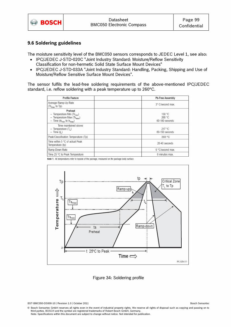
Datasheet
BMC050 Electronic Compass Page 99
Confidential
BST-BMC050-DS000-10 | Revision 1.0 | October 2011 Bosch Sensortec
© Bosch Sensortec GmbH reserves all rights even in the event of industrial property rights. We reserve all rights of disposal such as copying and passing on to
third parties. BOSCH and the symbol are registered trademarks of Robert Bosch GmbH, Germany.
Note: Specifications within this document are subject to change without notice. Not intended for publication.
9.6 Soldering guidelines
The moisture sensitivity level of the BMC050 sensors corresponds to JEDEC Level 1, see also:
IPC/JEDEC J-STD-020C "Joint Industry Standard: Moisture/Reflow Sensitivity Classification for non-hermetic Solid State Surface Mount Devices"
IPC/JEDEC J-STD-033A "Joint Industry Standard: Handling, Packing, Shipping and Use of Moisture/Reflow Sensitive Surface Mount Devices".
The sensor fulfils the lead-free soldering requirements of the above-mentioned IPC/JEDEC standard, i.e. reflow soldering with a peak temperature up to 260°C.
Figure 34: Soldering profile

Datasheet
BMC050 Electronic Compass Page 100
Confidential
BST-BMC050-DS000-10 | Revision 1.0 | October 2011 Bosch Sensortec
© Bosch Sensortec GmbH reserves all rights even in the event of industrial property rights. We reserve all rights of disposal such as copying and passing on to
third parties. BOSCH and the symbol are registered trademarks of Robert Bosch GmbH, Germany.
Note: Specifications within this document are subject to change without notice. Not intended for publication.
9.7 Handling instructions
Micromechanical sensors are designed to sense acceleration with high accuracy even at low amplitudes and contain highly sensitive structures inside the sensor element. The MEMS sensor can tolerate mechanical shocks up to several thousand g. However, these limits might be exceeded in conditions with extreme shock loads such as e.g. hammer blow on or next to the sensor, dropping of the sensor onto hard surfaces etc. We recommend avoiding g-forces beyond the specified limits during transport, handling and mounting of the sensors in a defined and qualified installation process. This device has built-in protections against high electrostatic discharges or electric fields (e.g. 2kV HBM); however, anti-static precautions should be taken as for any other CMOS component. Unless otherwise specified, proper operation can only occur when all terminal voltages are kept within the supply voltage range. Unused inputs must always be tied to a defined logic voltage level.

Datasheet
BMC050 Electronic Compass Page 101
Confidential
BST-BMC050-DS000-10 | Revision 1.0 | October 2011 Bosch Sensortec
© Bosch Sensortec GmbH reserves all rights even in the event of industrial property rights. We reserve all rights of disposal such as copying and passing on to
third parties. BOSCH and the symbol are registered trademarks of Robert Bosch GmbH, Germany.
Note: Specifications within this document are subject to change without notice. Not intended for publication.
9.8 Tape and reel specification
9.8.1 Tape and reel dimensions
The following picture describes the dimensions of the tape used for shipping the BMC050 sensor device. The material of the tape is made of conductive polystyrene (IV).
Figure 35: Tape and reel dimensions in mm

Datasheet
BMC050 Electronic Compass Page 102
Confidential
BST-BMC050-DS000-10 | Revision 1.0 | October 2011 Bosch Sensortec
© Bosch Sensortec GmbH reserves all rights even in the event of industrial property rights. We reserve all rights of disposal such as copying and passing on to
third parties. BOSCH and the symbol are registered trademarks of Robert Bosch GmbH, Germany.
Note: Specifications within this document are subject to change without notice. Not intended for publication.
9.8.2 Orientation within the reel
Figure 36: Orientation of the BMC050 devices relative to the tape
124
AYWW
CCC
124
AYWW
CCC
124
AYWW
CCC
124
AYWW
CCC
124
AYWW
CCC

Datasheet
BMC050 Electronic Compass Page 103
Confidential
BST-BMC050-DS000-10 | Revision 1.0 | October 2011 Bosch Sensortec
© Bosch Sensortec GmbH reserves all rights even in the event of industrial property rights. We reserve all rights of disposal such as copying and passing on to
third parties. BOSCH and the symbol are registered trademarks of Robert Bosch GmbH, Germany.
Note: Specifications within this document are subject to change without notice. Not intended for publication.
9.9 Environmental safety
The BMC050 sensor meets the requirements of the EC restriction of hazardous substances (RoHS) directive, see also:
Directive 2002/95/EC of the European Parliament and of the Council of 27 January 2003 on the restriction of the use of certain hazardous substances in electrical and electronic equipment.
9.9.1 Halogen content
Results of chemical analysis indicate that the BMC050 contains less than 900ppm (by weight) of Fluorine, Chlorine, Iodine and Bromine. Therefore the BMC050 can be regarded as halogen-free. For more details on the analysis results please contact your Bosch Sensortec representative.
9.9.2 Internal package structure
Within the scope of Bosch Sensortec‟s ambition to improve its products and secure the mass product supply, Bosch Sensortec qualifies additional sources (e.g. 2nd source) for the LGA package of the BMC050. While Bosch Sensortec took care that all of the technical packages parameters are described above are 100% identical for all sources, there can be differences in the chemical content and the internal structural between the different package sources. However, as secured by the extensive product qualification process of Bosch Sensortec, this has no impact to the usage or to the quality of the BMC050 product.

Datasheet
BMC050 Electronic Compass Page 104
Confidential
BST-BMC050-DS000-10 | Revision 1.0 | October 2011 Bosch Sensortec
© Bosch Sensortec GmbH reserves all rights even in the event of industrial property rights. We reserve all rights of disposal such as copying and passing on to
third parties. BOSCH and the symbol are registered trademarks of Robert Bosch GmbH, Germany.
Note: Specifications within this document are subject to change without notice. Not intended for publication.
10. Legal disclaimer
10.1 Engineering samples
Engineering Samples are marked with an asterisk (*) or (e) or (E). Samples may vary from the valid technical specifications of the product series contained in this data sheet. They are therefore not intended or fit for resale to third parties or for use in end products. Their sole purpose is internal client testing. The testing of an engineering sample may in no way replace the testing of a product series. Bosch Sensortec assumes no liability for the use of engineering samples. The Purchaser shall indemnify Bosch Sensortec from all claims arising from the use of engineering samples.
10.2 Product use
Bosch Sensortec products are developed for the consumer goods industry. They may only be used within the parameters of this product data sheet. They are not fit for use in life-sustaining or security sensitive systems. Security sensitive systems are those for which a malfunction is expected to lead to bodily harm or significant property damage. In addition, they are not fit for use in products which interact with motor vehicle systems. The resale and/or use of products are at the purchaser‟s own risk and his own responsibility. The examination of fitness for the intended use is the sole responsibility of the Purchaser. The purchaser shall indemnify Bosch Sensortec from all third party claims arising from any product use not covered by the parameters of this product data sheet or not approved by Bosch Sensortec and reimburse Bosch Sensortec for all costs in connection with such claims. The purchaser must monitor the market for the purchased products, particularly with regard to product safety, and inform Bosch Sensortec without delay of all security relevant incidents.
10.3 Application examples and hints
With respect to any examples or hints given herein, any typical values stated herein and/or any information regarding the application of the device, Bosch Sensortec hereby disclaims any and all warranties and liabilities of any kind, including without limitation warranties of non-infringement of intellectual property rights or copyrights of any third party. The information given in this document shall in no event be regarded as a guarantee of conditions or characteristics. They are provided for illustrative purposes only and no evaluation regarding infringement of intellectual property rights or copyrights or regarding functionality, performance or error has been made.

Datasheet
BMC050 Electronic Compass Page 105
Confidential
BST-BMC050-DS000-10 | Revision 1.0 | October 2011 Bosch Sensortec
© Bosch Sensortec GmbH reserves all rights even in the event of industrial property rights. We reserve all rights of disposal such as copying and passing on to
third parties. BOSCH and the symbol are registered trademarks of Robert Bosch GmbH, Germany.
Note: Specifications within this document are subject to change without notice. Not intended for publication.
11. Document history and modification
Rev. No Chapter Description of modification/changes Date
0.1 Document creation 2010-08-12
0.3 New revision 2011-03-07
0.4 New revision 2011-03-29
0.5 New revision 2011-06-15
0.6 New revision 2011-07-28
0.7 New revision 2011-10-13
1.0 Not longer under preliminary status 2011-10-28
Bosch Sensortec GmbH
Gerhard-Kindler-Strasse 8
72770 Reutlingen / Germany
www.bosch-sensortec.com
Modifications reserved | Printed in Germany
Specifications subject to change without notice
Document number: BST-BMC050-DS000-10
Revision_1.0_102011