Embed Size (px)
Citation preview

1
Module-1 BJT AC Analysis:
BJT AC Analysis: BJT AC Analysis: BJT Transistor Modeling, The re transistor model,
Common emitter fixed bias, Voltage divider bias, Emitter follower configuration. Darlington
connection-DC bias; The Hybrid equivalent model, Approximate Hybrid Equivalent Circuit-
Fixed bias, Voltage divider, Emitter follower configuration; Complete Hybrid equivalent model,
Hybrid π Model.
BJT Transistor Modeling
A model is an equivalent circuit that represents the AC characteristics of the transistor.
Transistor small signal amplifiers can be considered linear for most application.
A model is the best approximate of the actual behavior of a semiconductor device under
specific operating conditions, including circuit elements
Transistor Models
re- model – any region of operation, fails to account for output impedance, less accuracy
Hybrid model – limited to a particular operating conditions, more accuracy
The re Transistor Model
BJTs are basically current-controlled devices; therefore the re models uses a diode and a current
source to duplicate the behavior of the transistor. One disadvantage to this model is its sensitivity to the DC level. This model is designed for specific circuit conditions.
Common-Base Configuration
(a)
(b)
(c)
(d)
Figure 1 Common Base transistor re mode

2
We know that from diode equation re is defined as follows
Applying KVL to input and out circuit of figure 1(d), we will get
input impedance:
Output impedance:
Voltage gain:
=
Current gain:
Common-Emitter Configuration
(a)
(b)
(c)
(d)
Figure 2 Common Emitter re model of npn transistor

3
Figure 1 (a) shows simple transistor circuit. Figure 1(b) and 1(c) shows evaluation transistor re
model in CE configuration.
Applying KVL to input and out circuit of figure 2(d), we will get
input impedance:
Output impedance:
Voltage gain:
IbRLRLIcIoRLVo
ebiii rIZIV
eb
Lb
i
ov
rI
RI
V
VA
e
Lv
r
RA
Ib
Ib
Ib
Ic
Ii
IoAi
gain,Current
iA

4
Fixed bias Common-Emitter Configuration
(a)
(b)
Figure 3 Fixed bias Common-Emitter Configuration
Note in Fig. 3 (a) that the common ground of the dc supply and the transistor emitter terminal permits the
relocation of RB and RC in parallel with the input and output sections of the transistor, respectively. In addition,
note the placement of the important network parameters Zi, Zo, Ii, and Io on the redrawn network. Substituting
the re model for the common-emitter configuration of Fig. 3(a) will result in the network of Fig. 3(b). • From the above re model, Input impedance
Zi = [RB re] ohms
If RB > 10 re, then,
[RB re] re
Then, Zi re
Output impedance
Zo is the output impedance when Vi =0. When Vi =0, ib =0, resulting in open circuit equivalence
for the current source.
Zo = [RCro ] ohms
Voltage gain
Vo = - Ib( RC ro)
• From the re model, Ib = Vi / re
• thus,
– Vo = - (Vi / re) ( RC ro)
– AV = Vo / Vi = - ( RC ro) / re
10
• If ro >10RC,
– AV = - ( RC / re)
• The negative sign in the gain expression indicates that there exists 180o phase shift between the
input and output. Current gain:

5
Common-Emitter Voltage-Divider Bias
(a)
(b)
Figure 4 Voltage Divider bias Common-Emitter Configuration
The re model is very similar to the fixed bias circuit except for RB is R1R2 in the case of voltage
divider bias.
Input impedance:
Output impedance:
Voltage gain: From the re model, Ib = Vi / re thus,
Vo = - (Vi / re) ( RC ro)
Current gain:
6
( )( )
( ) if
if
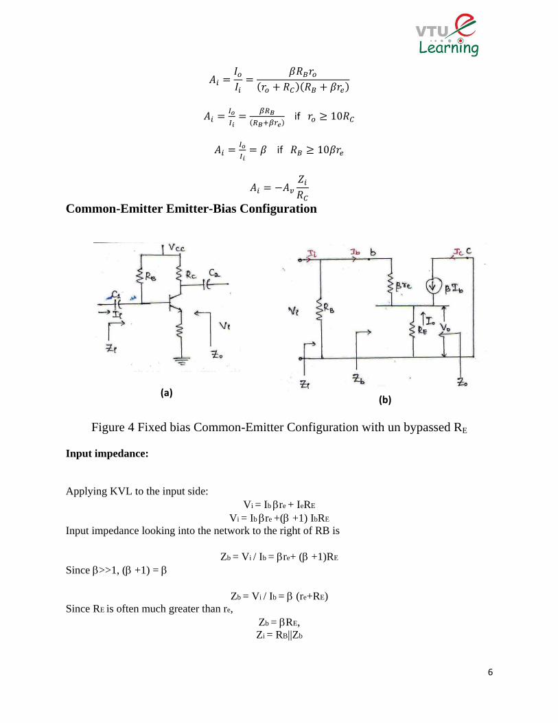
Common-Emitter Emitter-Bias Configuration
(a) (b)
Figure 4 Fixed bias Common-Emitter Configuration with un bypassed RE
Input impedance:
Applying KVL to the input side:
Vi = Ib re + IeRE
Vi = Ib re +(+1) IbRE Input impedance looking into the network to the right of RB is
Zb = Vi / Ib = re+ (+1)RE
Since >>1, (+1) =
Zb = Vi / Ib = (re+RE)
Since RE is often much greater than re,
Zb = RE,
Zi = RB||Zb
7
Output impedance: Zo is determined by setting Vi to zero, Ib = 0 and Ib can be replaced by open
circuit equivalent. The result is,
Voltage gain:
We know that, Vo = - IoRC
= - IbRC
= - (Vi/Zb)RC
AV = Vo / Vi = - [RC /(re + RE)]
RE >>re, AV = Vo / Vi = - [RC /RE]
Substituting, Zb = (re + RE)
( )
( )
Phase relation: The negative sign in the gain equation reveals a 180o phase shift between input
and output.
Current gain:
( )
Darlington Emitter Follower This is also known as the common-collector configuration.
• The input is applied to the base and the output is taken from the emitter. There is no phase shift
between input and output.

8
(a)
(b)
(c)
Figure 5 Darlington Emitter Follower
Input impedance:
Zi = RB || Zb
Zb = re+ ( +1)RE
Zb = (re+ RE)
Since RE is often much greater than re,
( )
Output impedance: To find Zo, it is required to find output equivalent circuit of the emitter follower at its input
terminal.
This can be done by writing the equation for the current Ib.
Ib = Vi / Zb
Ie = ( +1)Ib
= ( +1) (Vi / Zb)
We know that, Zb = re+ ( +1)RE substituting this in the equation for Ie we get,
Ie = ( +1) (Vi / Zb) = ( +1) (Vi / re+ ( +1)RE )

9
Ie = Vi / [ re/ ( +1)] + RE
Since ( +1) = ,
Ie = Vi / [re+ RE]
Using the equation Ie = Vi / [re+ RE] , we can write the output equivalent circuit as,
if
Since RE is typically much greater than re,
Voltage gain:
Using voltage divider rule for the equivalent circuit,
Vo = Vi RE / (RE+ re)
AV = Vo / Vi = [RE / (RE+ re)]
Since (RE+ re) RE,
AV [RE / (RE] 1
Phase relationship As seen in the gain equation, output and input are in phase
Current gain:
( )

10
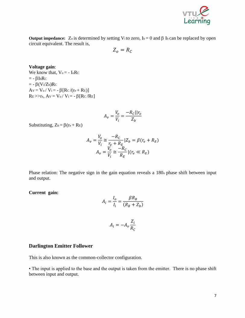
H – Parameter model :-
→ The equivalent circuit of a transistor can be dram using simple approximation by
retaining its essential features.
→ These equivalent circuits will aid in analyzing transistor circuits easily and rapidly.
Two port devices & Network Parameters:-
→ A transistor can be treated as a two part network. The terminal behaviour of any two
part network can be specified by the terminal voltages V1 & V2 at parts 1 & 2 respectively and
current i1 and i2, entering parts 1 & 2, respectively, as shown in figure.
Figure 6 Two port Network
Hybrid parameters (or) h – parameters:-
If the input current i1 and output Voltage V2 are takes as independent variables, the input voltage
V1 and output current i2 can be written as
V1 = h11 i1 + h12 V2

11
i2 = h21 i1 + h22 V2
The four hybrid parameters h11, h12, h21 and h22 are defined as follows.
h11 = [V1 / i1] with V2 = 0 Input Impedance with output part short circuited.
h22 = [i2 / V2] with i1 = 0 Output admittance with input part open circuited.
h12 = [V1 / V2] with i1 = 0 reverse voltage transfer ratio with input part open circuited.
h21 = [i2 / i1] with V2 = 0 Forward current gain with output part short circuited.
The dimensions of h – parameters are as follows:
h11 - Ω
h22 – mhos
h12, h21 – dimension less.
as the dimensions are not alike, (ie) they are hybrid in nature, and these parameters are called as
hybrid parameters.
i= 11 = input ; o = 22 = output ;
f = 21 = forward transfer ; r = 12 = Reverse transfer.
Notations used in transistor circuits:-
hi = h11 = Short circuit input impedance
h0 = h22 = Open circuit output admittance
hr = h12 = Open circuit reverse voltage transfer ratio
hf = h21= Short circuit forward current Gain.
The Hybrid Model for Two-port Network:-
V1 = h11 i1 + h12 V2
I2 = h1 i1 + h22 V2
V1 = h1 i1 + hr V2

12
I2 = hf i1 + h0 V2
Transistor Hybrid model:-
Essentially, the transistor model is a three terminal two – port system.
The h – parameters, however, will change with each configuration.
To distinguish which parameter has been used or which is available, a second subscript has been
added to the h – parameter notation.
For the common – base configuration, the lowercase letter b is added, and for common emitter and
common collector configurations, the letters e and c are used respectively.
Normally ℎris a relatively small quantity, its removal is approximated by ℎr and ℎrVo = 0, resulting in
a short – circuit equivalent.
The resistance determined by 1/ℎo is often large enough to be ignored in comparison to a parallel
load, permitting its replacement by an open – circuit quivalent.
CE Transistor Circuit
To Derive the Hybrid model for transistor consider the CE circuit shown in figure.The
variables are iB, ic, vB(=vBE) and vc(=vCE). iB and vc are considered as independent variables.
Then , vB= f1(iB, vc ) ----------------------(1)
iC= f2(iB, vc ) ----------------------(2)
Making a Taylor’s series expansion around the quiescent point IB, VC and neglecting
higher order terms, the following two equations are obtained.

13
ΔvB = (∂f1/∂iB)Vc . Δ iB + (∂f1/∂vc)IB . ΔvC ---------------(3)
Δ iC = (∂f2/∂iB)Vc . Δ iB + (∂f2/∂vc)IB . ΔvC ----------------(4)
The partial derivatives are taken keeping the collector voltage or base current constant as
indicated by the subscript attached to the derivative.
ΔvB , ΔvC , Δ iC , Δ iB represent the small signal(increment) base and collector voltages
and currents,they are represented by symbols vb , vc , ib and ic respectively.
Eqs (3) and (4) may be written as
Vb = hie ib + hre Vc
ic = hfe ib + hoe Vc
Where hie =(∂f1/∂iB)Vc = (∂vB/∂iB)Vc = (ΔvB /ΔiB)Vc = (vb / ib)Vc
hre =(∂f1/∂vc)IB = (∂vB/∂vc) IB = (ΔvB /Δvc) IB = (vb /vc) IB
hfe =(∂f2/∂iB)Vc = (∂ic /∂iB)Vc = (Δ ic /ΔiB)Vc = (ic / ib)Vc
hoe= (∂f2/∂vc)IB = (∂ic /∂vc) IB = (Δ ic /Δvc) IB = (ic /vc) IB
The above equations define the h-parameters of the transistor in CE configuration.The
same theory can be extended to transistors in other configurations.
Hybrid Model and Equations for the transistor in three different configurations are are
given below.
14
Comparision of H parameters

15
Analysis of transistor amplifier using h parameters.
For analysis of transistor amplifier we have to determine the following terms:
Current Gain
Voltage gain
Input impedance
Output impedance
Current gain:
For the transistor amplifier stage, Ai is defined as the ratio of output to input currents.

16
Input Impedence:
The impedence looking into the amplifier input terminals ( 1,1' ) is the input impedence Zi
Voltage gain:
The ratio of output voltage to input voltage gives the gain of the transistors.

17
Output Admittance: It is defined
Simplified Hybrid model is identical to the re model is as shown in fig. refer re model analysis
Hybrid versus re model: (a) common-emitter configuration
Hybrid model
The hybrid-pi or Giacoletto model of common emitter transistor model is given below. The
resistance components in this circuit can be obtained from the low frequency hparameters.
For high frequency analysis transistor is replaced by high frequency hybrid-pi model and
voltage gain, current gain and input impedance are determined.

18
This is more accurate model for high frequency effects. The capacitors that appear are
stray parasitic capacitors between the various junctions of the device. These capacitances
come into picture only at high frequencies.
• Cbc or Cu is usually few pico farads to few tens of pico farads.
• rbb includes the base contact, base bulk and base spreading resistances.
• rbe ( r), rbc, rce are the resistances between the indicated terminals.
• rbe ( r) is simply re introduced for the CE re model.
• rbc is a large resistance that provides feedback between the output and the input.
• r= re
• gm = 1/re
• ro = 1/hoe
• hre = r/ (r+ rbc)
The transconductance, gm, is related to the dynamic (differential) resistance, re, of the forward-
biased emitter-base junction:
gm = ∂Ic/∂Vb' e
= α∂Ie/∂Vb'e
≈α/re
≈Ic/Vth
Vth = kBT/q
The resistance rbb' is the base spreading resistance.
The resistance rb'c and the capacitance Cb'c (Cc ) represent the dynamic (differential) resistance
and the capacitance of the reverse-biased collector-base junction.

19
Using transconductance:
ic ≈ gm vb'e
(ignoring the current through rce )

20
Example 1 (a) Determine re. (b) Find Zi (c) Calculate Zo (d) Determine Av (e) Find Ai (f) Repeat parts (c) through (e)
including ro = 50 kΩ in all calculations and compare results. (From Text Book - Boylestad)

21
Example 2
22
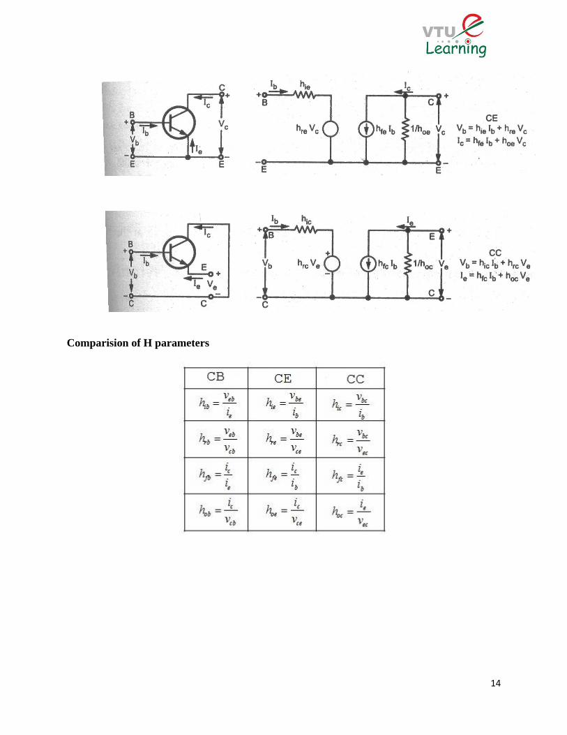
Example 3

23
Example 4
24
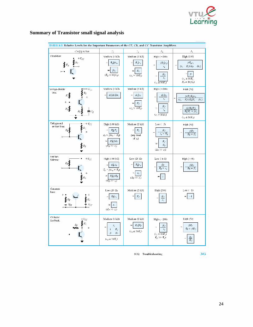
Summary of Transistor small signal analysis