Embed Size (px)
Citation preview

Biomolecular Layers on Silicon Studied
by Optical Spectroscopy
Dietrich R. T. Zahn and Simona D. Silaghi
Institut fur Physik, TU Chemnitz, 09107 Chemnitz, [email protected]
Summary. Amongst biomolecules the DNA base molecules adenine, cytosine, gua-nine, and thymine may also find interesting applications in organic electronics.They have optical gaps in the near ultra-violet and have already been considered ascharge transport molecules in organic field effect transistors. Still there is very littleknowledge on their electronic and optical properties when deposited as layers oninorganic substrates. Here the optical properties of the DNA bases deposited on flatand vicinal, hydrogen passivated Si(111) substrates are studied using spectroscopicellipsometry (SE) up to 9.5 eV photon energy employing synchrotron radiation andreflectance anisotropy spectroscopy (RAS). The results for the dielectric functionreveal strong optical anisotropy for adenine and guanine while the other two mole-cules form layers with isotropic properties. The experimentally derived dielectricfunctions are compared to density functional theory calculations of the optical re-sponse. Particularly interesting is the RAS response of the DNA bases as a functionof thickness when deposited on vicinal Si surfaces. Ordering in the layers is inducedby the step and terrace structure of the vicinal Si substrates. Even though themolecular structure is not dramatically different the RAS response is very distinctand allows an unambiguous identification of the bases.
1 Introduction
The usage of DNA base molecules as charge transport molecules in biomolecu-lar electronic and optoelectronic devices is still a challenge. Consequently, thedetermination of the dielectric functions of DNA base films by spectroscopicellipsometry (SE) is crucial for the understanding of both their electronicand optical properties. Recently, field effect transistor studies based on amodified DNA base revealed that the prototype bio-transistor gives rise to abetter voltage gain compared to carbon nanotubes (CNTs) [1]. The capabil-ity to fabricate structures with characteristic dimensions of a few nanometersis nevertheless a key prerequisite for future applications in nanoelectronics oras functional materials on a nanometer scale. With the reduced size of futuremolecular devices the effects of dimensionality are becoming more and moreimportant. Because silicon can be patterned in many ways, it is possible touse it as a versatile template and combine biomolecules with silicon electron-ics. Flat Si(111) has a 3-fold symmetry inducing the growth of three equiv-alent superstructure domains by symmetry but vicinal Si(111) surfaces can
B. Kramer (Ed.): Adv. in Solid State Phys. 45, 45–57 (2005)c© Springer-Verlag Berlin Heidelberg 2005

46 Dietrich R. T. Zahn
limit overlayer growth to a single domain. Moreover, vicinal surfaces shouldfavour the nucleation along the step edges, thus being potential substratesin controlling the ordering of molecules in so-called molecular nano-wires. Inthis sense, in situ reflectance anisotropy spectroscopy (RAS) is employed inultra-high vacuum (UHV) conditions for monitoring the ordering of DNAbase molecules on vicinal hydrogen passivated Si(111). Additionally, ab ini-tio calculations of electronic transitions corresponding to single DNA basemolecules carried out based on time-dependent (TD) density functional the-ory (DFT) methods employing the B3LYP method in combination with thebasis set 6-311++G(d, p) [2] are compared to the dielectric functions of theDNA base films.
2 Experimental and Data Analysis
Flat and vicinal p-type (B-doped) silicon(111) surfaces with resistivity in therange of 1–30 Ωcm were used as substrates for the DNA base films. One-side polished flat silicon substrates were provided by Wacker Siltronic whiledouble-side polished vicinal substrates were supplied by Silchem. Prior tobiomolecular deposition, the substrates were wet-chemically hydrogen termi-nated [3]. The “flat” Si(111) (0.35-off cut angle) surfaces were employed assubstrates for the thick biomolecular films and the investigation of their bulkoptical properties via spectroscopic ellipsometry. The vicinal Si(111) surfacesused as substrates for thin biomolecular films were off cut oriented by 3 and6, respectively, towards the [112] direction. The surface reconstruction waschecked by low energy electron diffraction (LEED). In the case of the vicinalsurfaces the LEED pattern shows a double splitting of the diffraction pointsin the [112] direction typical for the formation of steps and terraces. Thesource materials of high-purity DNA base powders purchased from Sigma-Aldrich were evaporated under UHV conditions (base pressure ∼ 10−8 Pa)from Knudsen cells. Molecules of thymine and cytosine were evaporated attemperatures of 365 and 410 K with corresponding evaporation rates of 0.8and 0.3 nm/min, respectively, while adenine and guanine molecules wereevaporated at temperatures of 400 and 510 K with evaporation rates of 1.5and 2 nm/min, respectively. The evaporation rates were in situ monitoredvia a quartz crystal and then ex situ calibrated via both ellipsometry andatomic force microscopy film thickness measurements.
In situ as well as ex situ ellipsometry measurements were performed onbiomolecular films with thicknesses ranging from 40 to 120 nm. In situ VUV-SE measurements were carried out in the energy range between 4 and 9.5 eVunder an incidence angle of 67.5 using synchrotron radiation as light sourceat BESSY II. Afterwards, the biomolecular films were investigated ex situvia variable angle spectroscopic ellipsometry (VASE) in the energy range of0.8–5 eV. Spectroscopic ellipsometry measures the change in polarization oflight as a function of incident angle and wavelength [4]. The experimentally

Biomolecular Layers on Silicon Studied by Optical Spectroscopy 47
determined ellipsometric values are Ψ and ∆, which are related to the ratioof Fresnel reflection coefficients rp and rs for p- and s-polarized light, respec-tively, by ρ = rp
rs= tan Ψei∆. The effective dielectric function is connected
with the measured ratio of Fresnel reflection coefficients ρ and incident angleφ0 by the following expression:
〈ε〉 = 〈ε1〉 + i〈ε2〉 = (〈n〉 + i〈k〉)2 = sin2 φ0
[1 + tan2 φ0
(1 − ρ
1 + ρ
)2]
(1)
The dielectric functions of the materials are determined by first constructinga suitable optical model of the sample with physically meaningful structuraland optical parameters, and then by iteratively adjusting these parametersto obtain the best fit to the measured ellipsometric data, i.e., the fitting withthe minimum mean square error MSE:
MSE =1
2N − M
N∑i=1
⎡⎣
(Ψmod
i − Ψexpi
σexpΨ,i
)2
−(
∆modi − ∆exp
i
σexp∆,i
)2⎤⎦ (2)
where N is the number of measured (Ψ, ∆) pairs and M is the total num-ber of real fit parameters. The ellipsometry results of the DNA base filmswere modelled via mathematical models implemented in the WVASE soft-ware in the energy range between 0.8 and 9.5 eV. Knowing the correspondingvalues for film thickness and surface roughness the experimental data werethen fitted using an Gaussian oscillator model which ensures Kramers-Kronigconsistency of the dielectric function in the entire range from 0.8 to 9.5 eV.Specifically, the optical properties of thymine and cytosine films were evalu-ated using an isotropic model meaning that the optical response of the sampleis equivalent in all three directions x, y, and z. On the other hand, the adenineand guanine films were described by a uniaxial anisotropic model consistingof two sets of Gaussian oscillators corresponding to ordinary (⊥ [111]) andextraordinary (‖ [111]) contributions. In order to derive accurate optical con-stants a multi-sample analysis (MSA) procedure was employed [5], [6]. Thisprocedure assumes that the same set of optical constants describes a set ofseveral films with different thicknesses which are coupled together in the fit.
The molecular ordering of DNA base molecules on both vicinal and “flat”H:Si(111) surfaces was monitored in situ during the growth by reflectanceanisotropy spectroscopy (RAS) in the energy range of 1.5–5.5 eV. RAS mea-sures the difference in normal incidence in reflection for light linearly polarizedalong two orthogonal directions in the sample surface. In the case of a vicinalSi(111) surface the RAS signal can be expressed as follows:
∆r
r= Re
(∆r
r
)+ iIm
(∆r
r
)= 2
r[110] − r[112]
r[110] + r[112]
(3)
Due to the fact that RAS is performed in normal incidence the techniqueis very sensitive to surface changes and capable of measuring very small

48 Dietrich R. T. Zahn
optical anisotropies of 10−3 or even smaller which are hardly detectable byellipsometry.
3 Results
3.1 Spectroscopic Ellipsometry
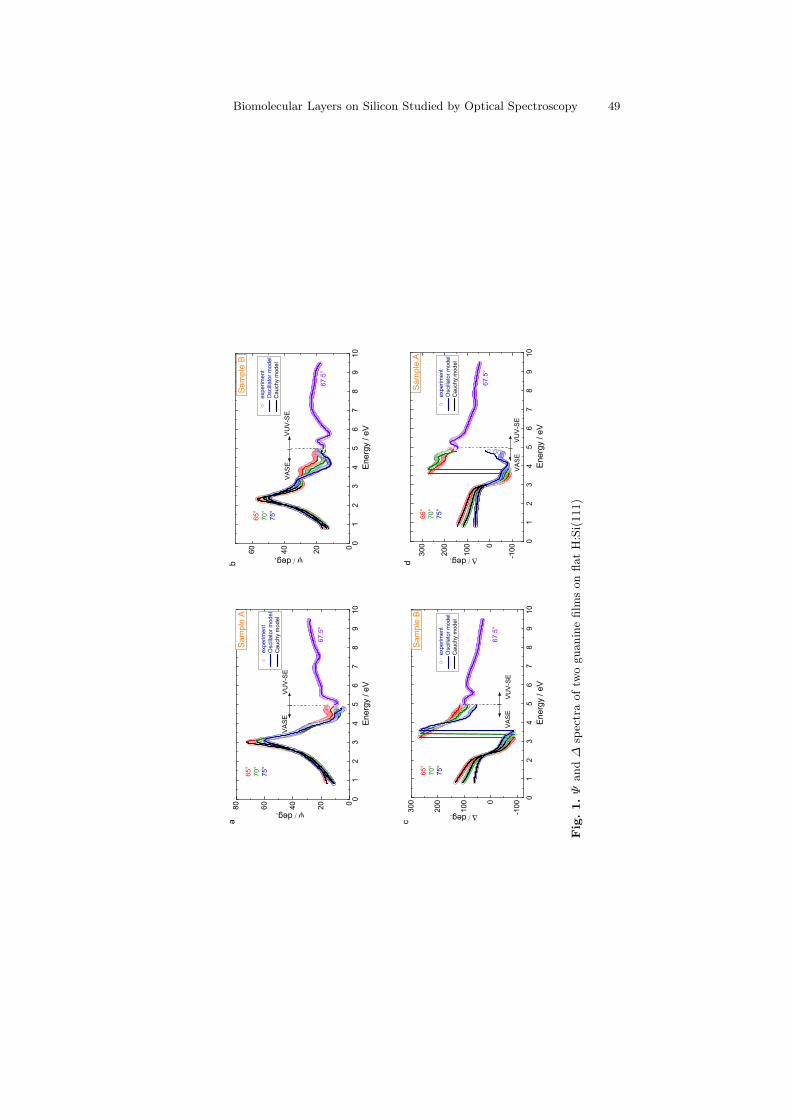
Figure 1 shows an example of ellipsometry data evaluation of two guaninesamples having film thicknesses of (61.7 ± 0.1) and (84.8 ± 0.1) nm corre-sponding to samples denoted as A and B. The optical response of guaninefilms was described by a uniaxial model. A MSE value of 7.655 was obtainedby the fitting procedure of both Ψ and ∆ spectra in the energy range of0.8–9.5 eV.
The dielectric function derived for guanine films is included in Fig. 2atogether with the corresponding dielectric functions of adenine (Fig. 2b), cy-tosine (Fig. 2c) and thymine (Fig 2d) films. Besides guanine, adenine filmsexhibit also strong optical anisotropy with the ordinary (⊥ [111]) compo-nent of the dielectric function being larger compared to the extraordinary(‖ [111]) component. This situation indicates a mainly planar orientation ofboth molecules with respect to the silicon substrate. From the ratio betweenthe extraordinary and ordinary components of the first band in ε2 the aver-age molecular orientation can be deduced. Thus, the molecular planes makean average tilt angle of ∼ 10 for adenine and ∼ 16 for guanine moleculeswith respect to the substrate plane. The preferential orientation of guanineand adenine molecules on H:Si(111) is additionally supported by the X-raydiffraction (XRD) results (not shown here). The interplanar spacing deter-mined as 3.29 Ais quite close to the interplanar distance between two stackedguanines in the guanine monohydrate crystal which is 3.30 A[7]. The favouredplanar orientation of the guanine was in addition observed on other kind ofsubstrates such as Cu(111) where the molecules order in a one-dimensional-like structure [8] or on substrates like MoS2 [9] and SrTiO3(100) [10]. In thecase of adenine films, the interplanar spacing derived from XRD matches thedistance of 3.30 Abetween stacked molecules. Generally, the adenine mole-cules prefer to lie down on various substrates e.g. KBr(100) [17], SrTiO3(100)[10], MoS2(0001) [18], HOPG [19].
In contrast to the strong anisotropy revealed by adenine and guanine films,the small molecules cytosine and thymine seem to form isotropic films. Thedielectric functions determined from ellipsometry data are compared with thecalculated electronic spectra (circles) of single DNA base molecules in Fig. 2.For a better comparison the initial calculated values of the energy positionsindicated by bars in Fig. 2 were red-shifted. In each case, the first theoreticalelectronic transition having π → π∗ character is assigned to the highestoccupied molecular orbital (HOMO) → lowest unoccupied molecular orbital(LUMO) band gap. In the case of the guanine molecule this is calculated to
Biomolecular Layers on Silicon Studied by Optical Spectroscopy 49
Fig
.1.
Ψand
∆sp
ectr
aoftw
oguanin
efilm
son
flat
H:S
i(111)

50
Dietrich
R.T
.Zahn
Fig. 2. Dielectric functions of (a) guanine, (b) adenine, (c) cytosine, and (d) thymine films. The calculated electronic spectra (circles)using TD-DFT were simulated using a sum of Gaussian oscillators with a FWHM of 0.2 eV. For a better comparison, the calculatedresults were red-shifted by (a) 0.65 eV, (b) 0.51 eV, (c) 0.18 eV, and (d) 0.55 eV

Biomolecular Layers on Silicon Studied by Optical Spectroscopy 51
be at 4.96 eV. The previous experimental results revealed the first absorptionband in the energy range from 4.31 to 4.59 eV [11, 12, 13, 14, 15, 16] whilefrom ellipsometry measurements the HOMO-LUMO band gap appears at 4.31eV being modelled by a Gaussian oscillator employed perpendicular to [111].A slightly higher optical band gap of 4.47 eV is measured by ellipsometry inthe case of adenine films but still lower than the previous reported resultswith energy values ranging from 4.51 to 4.63 eV depending on the surroundingenvironment of molecules [11, 12, 14, 20, 21]. For instance, the highest valueof 4.63 eV is observed for the adenine in aqueous solution [11]. The calculatedvalue for the HOMO → LUMO band gap of 4.98 eV is fairly high compared tothe experimental values. The highest optical absorption onset was observedfrom ellipsometry at 4 eV in the case of adenine while the lowest at around 3eV is characteristic for cytosine. Beyond 4 eV the imaginary part of dielectricfunction ε2 of cytosine exhibits mainly three structures in agreement withthose reported in the literature. The first band at 4.46 eV corresponds to theHOMO → LUMO band gap with the corresponding theoretical electronictransition at 4.64 eV. The experimental investigations performed on cytosinein various environments revealed a first absorption band in the energy rangebetween 4.40 and 4.70 eV [11, 12, 14, 15, 21, 22, 23, 24, 25, 26]. Above9 eV one can notice that the real part of the dielectric function ε1 of thecytosine film clearly shows an ascending behaviour. Indeed, the ultravioletreflectivity measurements performed in the energy range of 4–24 eV usingsynchrotron radiation on ∼ 1µm thick cytosine film on a mica substraterevealed additional structures above 9.5 eV [27]. The authors suggested thatthese additional structures must be due to σ → σ∗ transitions.
The imaginary part of the isotropic dielectric function ε2 of thymine cor-responding to thymine films reveals also mainly three bands in agreementwith the previous experimental data reported in the literature. The asymme-try of the first band in ε2 spectrum was modelled by two Gaussian oscillatorshaving energy positions at 4.44, and 4.64 eV, respectively. It was observedthat single crystal absorption measurements generate different energy posi-tions for the first absorption band when the incident electric field is polarizedalong different crystallographic axis [28]. For instance, the absorption alonga axis leads to a band centered at 4.5 eV while the absorption measuredalong b axis gives rise to another band at 4.38 eV. With the help of thesepolarization-dependent absorption investigations performed on a single crys-tal one can conclude that the doublet components observed at 4.44–4.64 eVin the case of thymine are an evidence of the crystalline nature of the filmrevealed additionally by XRD. Moreover, the doublet band observed in thethymine film seems to be mainly polarized in the ab crystallographic planewhich corresponds to the (001) plane [29]. Indeed, Ozeki et al. noticed thatfor instance the thymine anhydrate crystals grow as plates with (100) or (001)planes as prominent faces with the plane of the molecule being nearly parallelto the (001) plane [29]. The calculated HOMO → LUMO band gap of 4.99

52 Dietrich R. T. Zahn
Fig. 3. RAS spectra of various silicon surfaces
eV is quite high compared to previously experimental absorption bands re-ported at 4.8 eV in gas phase [22, 30], 4.7 eV in various solutions [21, 22, 30]4.64–4.44 eV in films [12], and 4.5 eV for a single crystal [28, 31]. Generally,the red-shift of the absorption from gas phase to single crystal is propor-tional with the increase of the intermolecular interaction by decreasing theintermolecular distances. Still, poor agreement in the relative intensities ofthe bands and energy positions is found when one compares TD-DFT cal-culations with the ε2 spectra of the DNA bases because the single moleculecalculations do not account for the intermolecular interactions so far.
3.2 Reflectance Anisotropy Spectroscopy
The anisotropy of cubic materials, e.g. silicon, arises at the surface due to abroken symmetry as in the case of vicinal Si(111) substrates where the surfaceanisotropy is induced by the formation of steps and terraces. Such anisotropyis often referred to as surface induced optical anisotropy (SIOA) [32, 33]. TheRAS signal of vicinal Si(111) surfaces is similar with the response of Si(110)surface as shown in Fig. 3. The fractional contribution of the [110] directionto the vicinality of (111) surface can be determined from the ratio betweenthe magnitude of the E2 peak for the vicinal surface and that for the (110)surface [3]. The values determined experimentally from the spectra are about0.08 and 0.17 corresponding to 3 and 6 off cut angles which are quite closeto the expected theoretical values of 0.09 and 0.18.
Figure 4 depicts the in situ RAS monitoring of DNA base layers on vicinalH:Si(111)-6 surfaces. During the RAS measurements the substrate geometrywas always kept identical with the one sketched in Fig. 3. All four molecules

Biomolecular Layers on Silicon Studied by Optical Spectroscopy 53
behave optically different when deposited onto the vicinal surface. Very smallanisotropies are observed in the case of guanine and cytosine in comparisonwith the large RAS signals arising from adenine and thymine layers. Whenincreasing the guanine coverage the RAS signal reaches a saturation level forthicknesses above 30 nm. The amplitude of the silicon features increases withthickness. Larger changes can be observed around the silicon E2 gap whichoverlaps with the absorption of guanine since the onset is around 3.5 eV.Moreover, the HOMO-LUMO gap of guanine at 4.31 eV is extremely closeto the 4.25 eV energy gap of silicon. The lineshape of the signal evolves in aderivative-like lineshape with increasing guanine coverage above 14 nm. Forcoverage above 20 nm the signal starts to decrease and finally saturates forthicknesses around 30 nm as shown in the inset of Fig. 4a. This can be relatedto the fact that the molecules form an isotropic layer and consequently thesignal vanishes due to equal absorption in orthogonal directions. In orderto distinguish between the anisotropy of the substrate and the anisotropyof the guanine films, RAS measurements of guanine deposition on almostflat H:Si(111)-0.35 were carried out (see Fig. 5a). The observed features areattributed to thickness artifacts. The weak anisotropy of guanine films onvicinal substrates seems to be caused by the vicinality which induces orderingof the guanine molecules up to critical thickness of about 20 nm. On thecontrary to guanine, adenine exhibits large anisotropy signals. By increasingthe adenine coverage the RAS signal evolves in a derivative-like lineshape inthe absorption range of adenine while the silicon features gradually vanish.The asymmetric evolution in the lineshape of the derivative-like RAS signalsindicates the contribution of at least two oscillators above 4 eV. Followingthe surface dielectric anisotropy model [34] it is found that the dominantabsorption takes place mainly along [112] direction suggesting furthermorestrong ordering of adenine molecules with respect to this direction. Weakanisotropy can be observed with a similar derivative-like lineshape also on thealmost flat silicon surface (Fig. 5b). Such small anisotropies were not observedby ellipsometry. The RAS monitoring of cytosine deposition on H:Si(111)-6
shows that the lineshape of the signal is strongly thickness-dependent as inthe case of guanine. Larger changes can be observed around the E2 gap ofsilicon at 4.25 eV which overlaps with the absorption of cytosine with theonset at 3 eV. At certain cytosine coverage a new feature around 4.90 eVappears which is closed to the second electronic transition at 4.95 eV asobtained from ellipsometry results.
For very thin cytosine coverages, the molecules seem to preferentially alignon vicinal surfaces with respect to the [110] direction. Already for highercoverage larger than 12 nm the signal starts to decrease and finally saturatesfor thicknesses around 20 nm as shown in inset Fig. 4c. There is no anisotropyof the cytosine layers on H:Si(111)-6 meaning that the anisotropy of cytosineon vicinal substrates is caused by the vicinality which induces ordering of thecytosine molecules up to critical thickness of about 10 nm. The strongest

54
Dietrich
R.T
.Zahn
Fig. 4. In situ RAS monitoring spectra of: (a) guanine, (b) adenine, (c) cytosine, and (d) thymine layers on H:Si(111)-6 surface

Bio
molecu
lar
Lay
erson
Silico
nStu
died
by
Optica
lSpectro
scopy
55Fig. 5. In situ RAS monitoring spectra of: (a) guanine, (b) adenine, (c) cytosine, and (d) thymine layers on “flat” H:Si(111)-0.35
surface

56 Dietrich R. T. Zahn
RAS signals were observed in the case of thymine layers on H:Si(111)-6 asreproduced in Fig. 4d. By increasing the thymine coverage the RAS signal ofthe substrate completely vanishes while large anisotropy signals appear in theabsorption range of the molecule. The lineshape of the RAS signal of thymineis very much like ε (see Fig. 2d). The negative sign of the signal suggests highabsorption along [112] direction and hence a preferential alignment of thetransition dipole moments of the molecule with respect to the parallel tothe same direction. Smaller anisotropies were also observed on “flat” siliconsubstrates but still larger signal amplitudes compared to the case of adeninelayers on the same type of substrate.
4 Summary
For the first time, the dielectric functions of all four DNA base films weresuccessfully determined in the energy range from near infrared to ultra-violet.Adenine and guanine films exhibit strong optical anisotropy being describedby a uniaxial dielectric function with a dominant ordinary component relativeto the extraordinary one and hence indicating a mainly planar orientation ofboth molecules with respect to the silicon substrate. The ellipsometry dataof thymine and cytosine films were described by an optically isotropic model.The calculations of electronic transitions gave rise to higher energy valuescompared to the ellipsometry results due to the fact that the single moleculecalculations do not account for the intermolecular interactions which usuallylead to a red-shift of energies. Furthermore, the RAS technique was employedfor the first time in monitoring the growth of DNA base molecules on both flatand vicinal H:Si(111) surfaces. The RAS measurements revealed informationabout the molecular ordering of DNA bases induced by the density of stepson silicon surfaces.
Acknowledgements
The financial support by Sachsisches Staatsministerium fur Wissenschaft undKunst (SMWK), Deutsche Forschungsgesellschaft Graduiertenkolleg GRK829/1 “Accumulation of Single Molecules to Nanostructures” and the BMBFproject 05 622 ESA2 is acknowledged. The BESSY facility is also acknowl-edged.
References
1. Mauricio, P. Visconti, V. Arima, S. D’Amico, A. Biasco, E. D’Amone, R. Cin-golani, and R. Rinaldi, Nanoletters 3, 479 (2003).
2. M. E. Casida, C. Jamorski, K. C. Casida, D. R. Salahub, J. Chem. Phys. 108,4439 (1998).

Biomolecular Layers on Silicon Studied by Optical Spectroscopy 57
3. Yasuda, D. E. Aspnes, D. R. Lee, C. H. Bjorkman, G. Lucovsky, J. Vac. Sci.Technol. A 12, 1152 (1994).
4. R. M. A. Azzam, N. M. Bashara: Ellipsometry and Polarized Light (Elsevier,North-Holland 1992).
5. M. A. Barret, Z. Borkowska, M. W. Humphreys and R. Parson, Thin SolidFilms 28, 137 (1986).
6. B. M. Ayupov, S. A. Prokhorova, Optics and Spectroscopy 90, 446 (2001).7. U. Thewalt, C. E. Bugg, R. E. Marsh, Acta Crsyt. B 27, 2358 (1971).8. M Furukawa, H. Tanaka, T. Kawai, J. Chem. Phys. 115, 3419 (2001).9. W. M. Heckl, Phys. Bl. 49, 417 (1993).
10. H. Tanaka, T. Kawai, J. Vac. Sci. Techol. B 13, 1411 (1995).11. D. Voet, W. B. Gratzer, R. A. Cox, P. Doty, Biopolymers 1, 193 (1963).12. T. Yamada, H. Fukutome, Biopolymers 6, 43 (1968).13. L. B. Clark, J. Am. Chem. Soc. 99, 3934 (1977).14. Y. Matsuoka, B. Norden, J. Phys. Chem. 86, 1378 (1982).15. C. A. Sprecher, W. C. Johnson, Biopolymers 16, 2243 (1977).16. J. C. Sutherland, K. Griffin, Biopolymers 23, 2715 (1984).17. J. T. Kim, M. Kanai, T. Kawai, and S. Kawai, Jpn. J. Appl. Phys. 33, 5027
(1993).18. S. J. Sowerby, M. Edelwirth, M. Reiter, W. M. Heckl, Langmuir 14, 5195 (1998).19. T. Uchihashi, T. Okada, Y. Sugawara, K. Yokoyama, S. Morita, Phys. Rev. B
60, 8309 (1999).20. L. B. Clark, J. Phys. Chem. 94, 2873 (1990).21. W. Voelter, R. Records, E. Bunnenberg, C. Djerassi, J. Am. Chem. Soc. 90,
6163 (1968).22. L. B. Clark, I. Tinoco Jr., J. Am. Chem. Soc. 87, 11 (1965).23. K. Raksanyi, I. Foldvary, J. Fidy, L. Kittler, Biopolymers 17, 887 (1978).24. T. P. Lewis, W. A. Eaton, J. Am. Chem. Soc. 93, 2054 (1971).25. F. Zaloudek, J. S. Novros, L. B. Clark, J. Am. Chem. Soc. 107, 7344 (1985).26. A. F. Fucaloro, L. S. Forster, J. Am. Chem. Soc. 93, 6443 (1971).27. D. E. Johnson, and M. Isaacson, Optics Communications 8, 406 (1973).28. B. G. Anex, A. F. Fucaloro, A. Dutta-Ahmed, J. Phys. Chem. 79, 2636 (1975),29. K. Ozeki, N. Sakabe, J. Tanaka, Acta Cryst. B 25, 1038 (1969).30. L. B. Clark, G. G. Peschel, I. Tinoco Jr., J. Phys. Chem. 69, 3615 (1965).31. J. S. Novros, L. B. Clark, J. Phys. Chem. 90, 5666 (1986).32. D. E. Aspnes, J. Vac. Sci. Technol. B 3, 1498 (1985).33. D. E. Aspnes, A. A. Studna, J. Vac. Sci. Technol. A 5, 546 (1987).34. R. J. Cole, B. G. Frederick, P. Weightman, J. Vac. Sci. Technol. A 16, 3088
(1998).