Embed Size (px)
Citation preview

Laser Photonics Rev. 6, No. 5, 607–621 (2012) / DOI 10.1002/lpor.201100031
LASER & PHOTONICSREVIEWS
Abstract Non-Gaussian beam profiles such as Bessel or an-nular beams enable novel approaches to modifying materialsthrough laser-based processing. In this review paper, proper-ties, generation methods and emerging applications for non-conventional beam shapes are discussed, including Bessel, an-nular, and vortex beams. These intensity profiles have importantimplications in a number of technologically relevant areas includ-ing deep-hole drilling, photopolymerization and nanopatterning,and introduce a new dimension for materials optimization andfundamental studies of laser-matter interactions. R
EVIEW
AR
TICLE
Bessel and annular beams for materials processingMarti Duocastella and Craig B. Arnold*
1. Introduction
1.1. General laser processing
Lasers have become indispensible for materials processingin scientific and industrial applications. They offer a highlydirectional and localized source of energy, which facilitatesmaterials modifications at precise locations [1]. Modernlaser systems are also flexible, in the sense that it is relativelyeasy to adapt parameters such as the beam size or the beamenergy to specific requirements, and systems can be scaledup to provide high throughput processing over multiplelength scales [2].
The typical laser parameters that are controlled for ma-terials processing include energy, fluence (energy per unitarea), spot size, wavelength, polarization and, in the caseof pulsed lasers, pulse duration and repetition rate [3, 4].The role of these parameters on the resulting structures andproperties has been widely studied, both experimentally andtheoretically [3, 5, 6] and such understanding is essential inorder to determine the optimum processing conditions. Forexample, laser fluence can affect the grain size of polycrys-talline silicon (poly-Si) obtained through laser annealingof amorphous silicon. This factor can drastically influencethe performance of poly-Si devices such as thin film tran-sitors [7]. The response of biological tissues is dependentupon the laser wavelength, affecting the performance ofsurgical techniques such as Laser In Situ Keratomileusis(LASIK) [8]. Beam polarization can influence absorptionin a given material [9], affecting the resultant structuresachieved through techniques such as laser cutting or weld-ing [10]. The rate at which energy is delivered in a materialalso affects the modification process [11]. In particular, the
laser pulse duration can have a significant effect on the ma-terial removal dynamics. This leads to a more rapid ejectionof material with a smaller heat affected zone as the temporalpulse length is shortened [12].
The control and influence of other laser parameters isless common yet these can also be important factors in ma-terials processing. One of these is the laser beam shape,defined as the irradiance distribution of the light when itarrives at the material of interest [13]. Although some lasersystems emit a multimode beam with a complex intensitydistribution, most commercial lasers provide either a Gaus-sian intensity profile (Fig. 1a), a “Top-hat” intensity profile(Fig. 1b), or are modified to fall into one of these two cate-gories.
1.2. Gaussian and Top-hat beams
Gaussian beams are by far the most common beam shapeused in materials processing. Notably, the Fourier transformremains a Gaussian and thus preserves its shape as it passesthrough an optical system consisting of simple lenses. Thisis especially important in laser processing, where multipleoptical elements are typically employed to guide the laserradiation to the workpiece.
Most lasers operate in the fundamental transverse elec-tromagnetic mode of the cavity (TEM00), and additionalelements are not needed to modify the beam shape. Sincethe output of a finite cavity will have some non-ideal charac-ter, a quality factor M2 (M2 � 1) is defined which indicateshow close a real beam is to a perfect Gaussian beam (M2=1).Typical scientific, solid state laser systems have M2 lessthan 2, however, industrial lasers with M2 less than 10 are
Department of Mechanical and Aerospace Engineering, Princeton University, Princeton, New Jersey 08544, USA* Corresponding author: e-mail: [email protected]
© 2012 by WILEY-VCH Verlag GmbH & Co. KGaA, Weinheim
608
LASER & PHOTONICSREVIEWS
M. Duocastella and C. B. Arnold: Structured light for processing
Figure 1 (online color at: www.lpr-journal.org) 2- and 3D intensitydistributions of: (a) Gaussian beam; (b) Top-hat beam; (c) Besselbeam; (d) annular or doughnut beam.
still considered to be high quality Gaussian sources [14]. Acommon approach to improving the beam quality is to em-ploy spatial filters [15]. However, for laser processing, theuse of a pinhole is less desirable as it reduces the availableenergy, requires precise alignment, and can be damaged byhigh laser intensities.
An important property of Gaussian beams for materialsprocessing is their low divergence, which allows for a smallfocused spot [16]. In fact, when focusing a Gaussian beamin air using a lens with a given numerical aperture NA thebeam diameter at the focus (d f ) can be expressed, as [1]:
d f ≈ 2λπ
M2
NA(1)
where λ is the wavelength of the laser radiation and wehave assumed that the beam fills the lens aperture (1/e crite-rion). Therefore, Gaussian beams with M2 close to 1 allowfor a minimal spot size and thus enable a higher resolutionthan other, higher mode beams. According to Eq. (1), for aperfect Gaussian beam with a wavelength of 1064 nm (com-mercial Nd:YAG laser) focused through an objective witha NA of 0.5, one can achieve a focal spot size as small as1.4 μm. This makes Gaussian beams ideal for microfabrica-tion applications.
Another important factor in the laser processing of ma-terials related to beam divergence, is the depth of field (z f ).In the context of materials processing, we can think of it
as the distance a workpiece can be moved away from thebeam waist while still maintaining the focal beam size. Morespecifically, it can be defined as the Rayleigh range, zr [17]:
z f = zr ≈ π4λ
d2f
M2. (2)
zr represents the distance from the beam waist along thepropagation direction at which the beam doubles its crosssectional area. For a 1064 nm laser with a Gaussian beamshape focused to a spot of 1.4 μm, the depth of field wouldbe approximately 1.4 μm. Compared to other cavity beammodes, low M2 beam have a relatively large depth of field,but under strong focusing conditions, the depth of field canstill be too short for many industrially important process-ing applications.
Top-hat beams are also widely used for materials pro-cessing applications. For instance, excimer lasers generallyproduce a Top-hat output with varying degrees of unifor-mity across the beam. Alternatively, optical elements areused such as beam shapers when the output beam from thelaser cavity is a Gaussian or homogenizer systems when theoutput is multimode. In comparison to Gaussians, Top-hatbeams have an M2 value much higher than 10. Thus, fromEqs. 1 and 2 it can be deduced that the minimum spot sizewill not be as small as with Gaussian beams, and that thedepth of field will not be as long. However, the improved spa-tial uniformity of Top-hat beams present important benefitsfor specific materials processing applications in comparisonto Gaussian beams [18]. This accounts for the preference ofthis type of beam for heat treatments such as laser anneal-ing [19], materials deposition such as in pulsed laser deposi-tion [20], welding applications with improved weld qualityand repeatability [21], and even photolithography [22].
One of the major challenges associated with Top-hatbeams is that unlike Gaussians, they do not maintain theirshape as they propagate, and thus they only present a uni-form intensity distribution near the focal point or imaginglocation of the optical system. Outside this zone, the beamprofile and quality vary, which can lead to nonuniform pro-cessing and undesired effects.
1.3. Need for other beam shapes
Non-conventional beam shapes have the advantage that theycan be explicitly designed to meet the requirements of agiven material configuration or application that could not befeasible with either Gaussian or Top-hat beams. An examplecan be found in the use of photomasks for large array holedrilling for thin film transistor displays [23]. The photomaskshapes a Top-hat beam into an array of beamlets, each witha uniform intensity distribution. Due to its parallel nature,this method reduces the processing time, and the uniformintensity distribution of each spot creates features with sharpedges. Beam shaping can also be an advantage in laser directwriting techniques such as laser-induced forward transfer(LIFT). In this technique, laser pulses are used to depositvolumetric pixels of material (voxels) from a donor film to
© 2012 by WILEY-VCH Verlag GmbH & Co. KGaA, Weinheim www.lpr-journal.org
Laser Photonics Rev. 6, No. 5 (2012)
REVIEWARTICLE
609
a receiver substrate [24]. Traditionally, LIFT is performedwith Gaussian [25] or Top-hat beams [26] that enables thefabrication of patterns through the successive deposition ofvoxels with computer controlled positioning accuracy. How-ever, recently, it has been demonstrated that one can depositvoxels with the specific shape of the incident beam [27].In this way, complex patterns can be directly printed byarbitrarily shaping the beam, reducing the processing timeand enabling high-throughput parallelization.
The possibilities that laser beam shaping offers are notlimited to the previous examples, nor the field of materi-als processing. In fact, different beam shapes have beensuccessfully used in several areas. For instance, the useof non-conventional beam shapes in optical manipulation,such as Bessel beams [28, 29] or Airy beams [30], has al-lowed the simultaneous trapping of several particles at thesame time or the transport of 60 μm microspheres over adistance of half a meter. Such performance is not possiblewith either Gaussian or Top-hat beam shapes. In atom op-tics, Laguerre-Gaussian or optical vortex light beams havebeen successfully used for atom guiding [31–33], and ithas been demonstrated that Bessel beams can produce elon-gated atom traps not achievable with Gaussian beams [34].The use of annular beams combined with Gaussian beamshas enabled novel imaging techniques such as stimulatedemission depletion (STED) microscopy [35, 36]. Finally,for novel applications in biology such as cell transfectionthrough optoinjection, the use of Bessel beams obviates theneed for accurate focusing on the soft cell membrane, thusmaking the overall process more efficient [37, 38].
One of the things to keep in mind with structured beamsfor materials processing is that most methods of shapingthe beam inevitably reduce the amount of energy availablefor modification. In this respect, Gaussian beams have anadvantage over any other beam shape as discussed above.However, the trade-off of reduced power associated withshaped beams may be more appropriate in certain cases,due to the unique material responses that they can generate.Therefore, beam shaping can be considered an importantcontrolling parameter in the pursuit of process optimization,as well as a viable approach to increase the flexibility oflasers, expanding their use in new and interesting directions.
1.4. Statement of paper direction
This present paper reviews emerging applications of Besseland annular beams in materials processing. These twobeams are closely related through their Fourier transformand exhibit unique properties that open the door to numer-ous opportunities in research and industrial applications.Such properties are discussed along with an analysis ofthe advantages and disadvantages these intensity profilespresent. In the first section of this review, the properties andthe methods to generate these beams are presented. Next, wereview recent work in materials processing for which Besseland annular beams are employed. Finally, we conclude witha discussion of the future outlook for Bessel and annularbeams laser processing.
2. Bessel and annular beams
For the purposes of this paper, we define a Bessel beam tomean a beam whose electric field is explicitly described bya zeroth-order Bessel function of the first kind (J0):
E(r,ϕ,z) = A0 exp(ikzz)J0(krr) (3)
where r and ϕ are transverse and polar coordinates, z is thecoordinate in the propagation direction, and kz and krarethe longitudinal and radial wavectors. More generally, theterm Bessel beam could refer to higher order functionsalthough we ignore those here. Since the beam intensity isproportional to the square of the electric field for a Besselbeam,
I(r,ϕ,z) ∝ J20 (krr) , (4)
this beam does not appear as a single spot, but rather as aseries of concentric rings (Fig. 1c). Another way to thinkabout a Bessel beam and its “bulls-eye” pattern, is to con-sider its formation as the result of the interference of planewaves with wave vectors belonging to a conical surface. Aregion of self-interference develops in which the Bessel pat-tern emerges due to cylindrical symmetry. It should also bepointed out that, according to Eq. (4), the number of ringsof a Bessel beam should be infinite. However, in laboratorygenerated Bessel beams the presence of finite apertures pro-duces Bessel beams with finite dimensions. In the presentpaper only these ‘finite Bessel beams’, also referred to asquasi-Bessel beams [39], will be considered. It is impor-tant to note that in the far field, as the separation betweenthe wavevectors increases, the beam intensity in the centralaxis decreases and eventually attains a null value, whichcorresponds to an annular beam.
An annular beam, also called doughnut-shaped beam,is a beam with an intensity distribution concentrated in aring with no on-axis intensity, as represented in Fig. 1d.There exist multiple sorts of annular beams depending onthe irradiance distribution within the annulus. For instance,the distribution can be constant in r and θ , in which case theannular beam is described by the equation:
I(r,θ) =
{I0 ri � r � ro
0 rest of points(5)
where I0 is the intensity within the annulus, r and θ are thepolar coordinates, and ri and ro the input and output beamradii, respectively. More commonly, annuli with a Gaussianprofile in the r direction are generated. The equation thatdescribes such beams is:
I(r,θ) = I0 exp
(−2
(r− rc)2
ω2
)(6)
where I0 is the maximum intensity of the beam, rc is theposition of I0, and ω is the beam waist. An annular beamcan also be formed by subtracting two Gaussian beams ofthe same maximum intensity but with different beam waists.In this case, the resulting beam intensity would be:
I(r,θ) = I0
[exp
(−2r2
ω21
)− exp
(−2r2
ω22
)](7)
www.lpr-journal.org © 2012 by WILEY-VCH Verlag GmbH & Co. KGaA, Weinheim
610
LASER & PHOTONICSREVIEWS
M. Duocastella and C. B. Arnold: Structured light for processing
where, ω1and ω2 correspond to beam waists of the twoGaussian beams.
A related structure to the annular beam is the so-calledoptical vortex (OV) beam. The discovery that a beam oflight with a well-defined orbital angular momentum canbe created rather easily in a laboratory [40] opened up thepossibility to study the role of this new optical parameter inlight-matter interactions [41]. An OV beam takes advantageof this property and is defined as a beam whose phase variesazimuthally along the direction of propagation. OV’s arecharacterized by their topological charge (m), which cor-responds to the number of twists in the phase front withinone wavelength. Due to the twisting of the phase front, thephase in the beam center is multiply defined, giving rise toan optical singularity that produces a vanishing amplitudeat this point [42] giving the appearance of an annulus inintensity.
It is important to note that the literature tends to take ageneral view to the term “annular beam” and uses it to referto any beam with a null intensity along the beam axis suchas OV beams. For instance, first order Bessel beams [43],whose intensity is proportional to the square of a first or-der Bessel function (J1), or higher order Laguerre-Gaussmodes [44] fall into this category. Such different annularbeams can lead to unique material responses [45] and there-fore one must use care in distinguishing experiments em-ploying this general class of intensity profile.
2.1. Properties of Bessel and annular beams
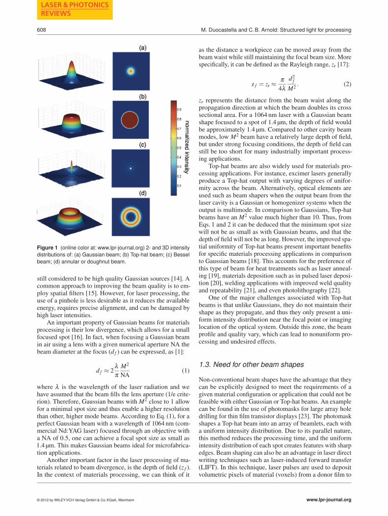
A detailed description of the properties of Bessel beams canbe found in [34] and [39]. Perhaps the most important opti-cal property for materials processing is the extended depthof field of Bessel beams. This ‘nondiffracting’ effect occursas a result of minimal spreading in the central lobe duringwave propagation [46, 47]. Such behavior is illustrated inFig. 2, in which an incident Gaussian beam either propa-gates through a converging lens to its focus, or is shapedinto a Bessel beam. The elements are selected such thatthe beam waist of the Gaussian is the same as the width ofthe central lobe of the Bessel beam (Fig. 2a). Although themaximum intensity along the principle axis is lower in thecase of the Bessel beam, the FWHM along the z-directionis orders of magnitude greater (1 cm vs 0.01 cm).
In fact, the Rayleigh range for a Bessel beam can beapproximated as:
zBessel ≈ πDd f
4λ(8)
where D is the diameter of the aperture, d f the diameter ofthe central lobe, and λ the laser wavelength [48]. ComparingEq. (8) with the corresponding Rayleigh range of a Gaussianbeam (Eq. (2)), it can be observed that Bessel beams have amuch larger Rayleigh range when D � d f , as it is usuallythe case. Thus, Bessel beams exhibit a greater depth of fieldthan Gaussian beams. The cost of this increased depth offield is that optical energy is distributed among the rings in
Figure 2 (online color at: www.lpr-journal.org) Simulations ofthe intensity distribution along the propagation distance z fromthe focusing objective of: (a) a Bessel beam generated using anaxicon (wedge angle of 12o) to focus a Gaussian beam (532 nm,ω0=1 mm) (b) same Gaussian beam focused using a microscopeobjective (NA of 0.25). Although the central lobe of the Besselbeam and the Gaussian beam have the similar radial dimensions,their differences are evident: the Bessel beam exhibits a longerdepth of field, whereas the maximum intensity of the Gaussianbeam in the focal region is higher.
the pattern and so the nondiffracting property of a Besselbeam comes at the expenses of power and contrast [46].However, as we will see below, the benefits of high-depthof field for applications such as deep hole drilling or manu-facturing on uneven surfaces outweighs these trade-offs.
A second optical property of Bessel beams that is theirability to reconstruct after an obstruction [28], in an effectthat is commonly called ‘self-healing’. This can be under-stood by considering the construction of a Bessel beam as asuperposition of plane waves propagating on a cone. In thisway, if an obstacle is placed in the center of the beam, it willblock some of the rays, but others will interfere again afterthe obstruction and reform the beam. This unique propertycan help to mitigate effects of debris and other products ofthe laser processing that can partially block incident beams.With conventional beams, such blocking can result in pro-cessing nonuniformities.
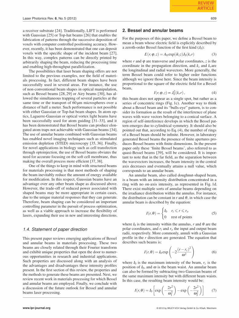
In the case of annular beams, the null intensity on-axishas important implications for thermal and mechanical ef-fects in materials [49, 50]. This is demonstrated in Fig. 3,where we simulate the temperature profiles of silicon af-ter 333 μs of irradiation with a CW laser with a Gaussianbeam (beam waist 800 μm), a Top-hat beam (diameter of800 μm) and with an annular beam (exterior beam diame-ter 800 μm). The Gaussian beam produces a temperatureincrease mainly in an area localized by the beam waist. Thesame occurs with a Top-hat beam, although the lateral ex-tent of the heated area is greater. When using an annularbeam, the lateral spreading of the heated area is still largerwhile the maximum temperature rise is lower in the center.
© 2012 by WILEY-VCH Verlag GmbH & Co. KGaA, Weinheim www.lpr-journal.org

Laser Photonics Rev. 6, No. 5 (2012)
REVIEWARTICLE
611
Figure 3 (online color at: www.lpr-journal.org) Simulations ofthe temperature profiles in silicon at 333 μs after depositing 1 Jof energy, assuming an absorption depth of 1 μm for: (a) Gaus-sian beam; (b) Top-hat beam; and (c) annular beam. (Thanks toMatthew Brown for generating this figure.)
These differences in the temperature profiles are crucial forapplications in which temperature is a key parameter, suchas laser heat treatment or laser hardening. It is also worthmentioning that when a material is irradiated with a CWlaser beam with an annular shape, the induced stress in thecenter of the irradiated area is minimal [51], a phenomenonthat does not occur with other beam shapes, and one that canbe employed in processes such as glass cutting for whichcontrolling stress is desired.
2.2. How to generate Bessel and annular beams
2.2.1. Aperture based methods
Bessel and annular beams can be generated using apertures.In fact, the first experimental realization of a Bessel beam
Figure 4 (online color at: www.lpr-journal.org) A plane wave isused to illuminate an annular aperture situated in the back focalplane of a convergent lens. As a result, a Bessel beam is formedin the image plane [48].
was achieved using this method [48], an annular slit wassituated in the back focal plane of a convergent lens and wasilluminated with a plane wave (Fig. 4). The electric field atthe aperture plane can be written as:
Eslit = Aiδ (r− rs) (9)
where Ai is the wave amplitude, δ is the Dirac delta function,and rs the slit diameter. The electric field at the front focalplane of the lens is proportional to the Fourier transform ofthe incident electric field [52]. Due to the circular symmetryof the system, this Fourier transform can be written as aFourier-Bessel transform,
Efront (r) =2πiλ f
∫ ∞
0r′Eslit
(r′)
J0
(2πr′ρ
)dr′ (10)
where the Fresnel diffraction formula has been employed,and ρ = r/λ f , with λ being the plane wave wavelength andf the lens focal distance. The solution of Eq. (10) is:
Efront (r) = Ai2πrs
iλ fJ0
(2πrsr
λ f
)(11)
which has the same form as Eq. (3), the definition of a Besselbeam.
Although successful in generating a Bessel beam, thismethod, is highly inefficient since the aperture blocks mostof the incident radiation. This reduction in the available en-ergy is unsuitable for applications where high intensities areneeded. Thus, for materials processing applications, othermethods are generally more desirable.
Annular beams can also be generated using apertures.Apart from the annular beam encountered in the far fieldof any finite Bessel beam, the introduction of an additionallens in the previous setup also allows the generation ofannular beam. The lens will produce the Fourier transformof a Bessel beam, which is an annular beam. Again, thelow throughput of this configuration is not favorable formaterials processing.
2.2.2. Axicons
An axicon, or conical lens element, as shown in Fig. 5 isperhaps the most convenient and cost-effective way to gen-erate a Bessel beam [53]. In this case, the incident beam
www.lpr-journal.org © 2012 by WILEY-VCH Verlag GmbH & Co. KGaA, Weinheim

612
LASER & PHOTONICSREVIEWS
M. Duocastella and C. B. Arnold: Structured light for processing
Figure 5 Creation of a Bessel beamusing an axicon illuminated with a Gaus-sian beam. If a convergent lens is placedafter the axicon, an annular beam is pro-duced in the lens focal plane.
is refracted in order to produce the interference pattern de-scribed earlier. This approach provides a more opticallyefficient way to produce a Bessel beam than aperture-basedmethods. However, the alignment between the incident laserbeam and the axicon is a critical issue, which can result innonuniformities if not properly aligned [31]. Usually, theincident beam is Gaussian, in which case the resulting beamafter the axicon is called Gaussian-Bessel, and its intensityprofile is [54, 55]:
I(r,z) = 2kπ(tan2 α
)(n−1)2zI0e−2(n−1)z tanα/ω0
× J20 (kr(n−1) tanα) (12)
where r and z are the radial and longitudinal coordinates,I0 and ω0 are the intensity and beam waist of the incidentGaussian beam, k is the wave vector, n the index of refrac-tion of the axicon material, and α is the wedge angle. Thisequation can be equivalently written in terms of the coneangle β at the tip of the axicon. Using Eq. (12) one candetermine the width of the central lobe by finding the firstzero of the Bessel function. This yields,
d f =2.4a
k(n−1) tan(α)(13)
where a is a constant of order unity. Substituting this intoEq. (8) for the Rayleigh range gives
zr ≈ D2(n−1) tan(α)
. (14)
Therefore, the wedge angle of an axicon ultimately deter-mines the waist and extent of the central lobe of the Besselbeam [56], with smaller angles corresponding to wider lobesand longer “diffractionless” propagation. For typically im-plementations in materials processing, this wedge angle issmall (< 0.1 rad).
Annular beams can also be formed with an axicon intwo different ways. The first one is to simply place the work-piece at a distance far enough from the axicon in order toencounter the far-field profile of the axicon which corre-sponds to an annulus. Alternatively, one can combine theaxicon with another focusing element to create an annulusat the focal plane of the system [57]. The outer diameter ofthe annulus generated in this way is given by:
d = 2F tan(α (n−1)) (15)
where F is the effective focal length of the lens [58]. Thislatter approach enables greater control over the size andshape of the annular beam.
Axicons can be either refractive or diffractive with theformer ones being widely adopted due to the relative simplic-ity of fabricating them. Recently, researchers have shownthe ability to produce a fluid based tunable device that allowsone to control the wedge angle of the axicon [59]. Diffrac-tive axicons are similar in construction to Fresnel lenses, andhave the advantage of being thinner than refractive axicons.Additionally, for ultrashort pulses commonly encounteredin materials processing, beams created by diffractive meth-ods are less likely to suffer broadening due to non-linearcharacteristics of the lens material [60].
2.2.3. SLM based methods
A spatial light modulator (SLM) is a digital device thatmodifies the phase and/or intensity of an incoming laserbeam. These devices have become popular for their abil-ity to produce arbitrary beam profiles and holograms forwide-spread applications in processing and imaging [61,62].One can easily produce a phase pattern in an SLM that cor-responds to a diffractive axicon, and as a result, the SLMwill generate Bessel or annular beams with user-definedwedge angles [63]. It is also possible to imprint a helicalramp phase with a central singularity [64], which allows thedirect formation of an optical vortex beam. There are differ-ent types of SLMs, such as magneto-optic SLMs [65], de-formable mirror SLMs [5], or liquid crystal (LC) SLMs [66].Although providing the widest range of intensity profiles,these devices tend to have relatively low damage thresh-olds limiting their applicability in materials processing tolow average power processes. The incorporation of a cool-ing system can help increase the damage threshold and hasenabled the use of higher powered nanosecond lasers formicromachining using SLMs [67].
2.2.4. TAG lens
A tunable acoustic gradient (TAG) lens provides an alter-native adaptive optical method of creating a user-definedBessel or annular beam. In the TAG an acoustic field is
© 2012 by WILEY-VCH Verlag GmbH & Co. KGaA, Weinheim www.lpr-journal.org

Laser Photonics Rev. 6, No. 5 (2012)
REVIEWARTICLE
613
Figure 6 (a) Index profile of the TAG lens atone instant in time and (b) half-period later in time.(c) Multiscale Bessel beam created by the TAGlens. The TAG lens is driven at a frequency of257 kHz, and a CW green laser is used for illumi-nation [72].
generated in a liquid chamber leading to a periodically vary-ing index of refraction profile in the device [68–71]. Whenusing a cylindrical chamber, this index can be written as
n(r, t) = n0 +nAJ0
(ωrv
)cos(ωt) (16)
where n0 corresponds to the static refractive index, ω to thedriving frequency, v to the speed of sound in the fluid, andnA is a constant that depends on the physical properties ofthe medium and the driving voltage amplitude (Fig. 6a,b).When light passes through this index of refraction profile,it is transformed into a multiscale Bessel beam [68] wherea central Bessel beam is formed surrounded by additionalBessel-like rings (Fig. 6c) [72]. The particular output patternof the TAG lens can be selected by synchronizing a pulsedlaser with the phase of operation of the TAG. Under theappropriate conditions, it can provide a simple Bessel orannular beam to be used for materials processing or imag-ing [73–75]. The properties of the TAG generated beamcan be modified by varying the frequency and/or ampli-tude of the lens driving signal. These parameters can berapidly changed and as such, the switching time of the TAGlens is on the order of microseconds [76], which makes itsignificantly faster than commercial SLMs.
2.2.5. Optical fibers
Optical fibers have been recently reported as a valid alter-native for the generation of Bessel or annular beams. Themain advantage of optical fibers compared with the previousmethods is the lack of free-space elements, which facilitatesintegration in miniaturized systems. Moreover, they havean added benefit in their inherent compatibility with therapid developing fiber lasers for materials processing appli-cations [77].
There exist multiple approaches to generate Besselbeams using optical fibers. For instance, one can fabricatean axicon on the tip of a fiber using chemical etching meth-ods [78,79] or by appropriately polishing the fiber tip [80]. ABessel beam can also be obtained by using a hollow opticalfiber with a polymer converging lens in its tip, in an analo-gous way to the aperture method described in 2.2.1 [81]. Theuse of multimode (MM) fibers provides a different approachto generate higher-order Bessel-like beams. In MM fibersthe excited modes, represented as LP0,n (n being the radial
index) correspond to zeroth order Bessel functions. Thus,the propagation of light in MM fibers produces interferencesbetween different fiber modes that result in a Bessel-likebeam with non-diffracting characteristics [82, 83]. Alterna-tively, it is possible to design a fiber that selects a singlehigh-order fiber mode (LP0,n,n>5), which is accomplishedusing long period fiber gratings [84, 85]. This approach of-fers a high conversion efficiency and allows the formationof beams with a high similarity to ideal Bessel beams [86].
Annular beams can be generated using any of the fiber-based approaches mentioned above at the far-field of thefiber output. In addition, there exist inherent annular beamgeneration methods using optical fibers. For instance, a fiberwith a small hollow in its center produces these beams [87].It is also possible to obtain an annular beam at the output ofa MM fiber (with a parabolic refractive index) illuminatedwith an input beam that presents a certain incidence anglewith respect to the fiber axis [88, 89]. The requirement ofsuch tilting, though, reduces the coupling efficiency and theoutput power, which can be detrimental for laser processingapplications.
2.2.6. Other methods
In addition to the more common methods mentioned abovefor materials processing, there are a number of alterna-tive ways to obtain Bessel or annular beams. Researchershave found success using pre-fabricated holographic dis-plays [90], diffractive optical elements [12, 91], opticalphase plates or spatial phase masks [92]. For OV beams,spiral phase plates (SPP), a dielectric material with a thick-ness that varies azimuthally around the plate have showngreat potential for high-intensity beam propagation [93]. Inaddition, uniaxial birefringent crystals [94], have allowedthe successful generation of high-intensity ultrafast vortexpulses without broadening, thereby providing a convenienttool to study material processing with OVs.
3. Applications of annular and Bessel beamsfor materials processing
Annular and Bessel beams enable unique material responses,which offer new fundamental insights in light-matter inter-actions and have the potential to extend the possibilities of
www.lpr-journal.org © 2012 by WILEY-VCH Verlag GmbH & Co. KGaA, Weinheim
614
LASER & PHOTONICSREVIEWS
M. Duocastella and C. B. Arnold: Structured light for processing
laser processing. In this section, we review recent works inlaser processing areas where these beams are providing anovel and unique alternative to traditional beam shapes.
3.1. Microdrilling
Laser drilling of micron-sized holes is a well-establishedindustrial process used in a number of applications rangingfrom car manufacturing to consumer electronics [95]. Laserfluences above the ablation threshold lead to direct materialremoval and the formation of a hole. The quality of the holedepends on both the properties of the irradiated material aswell as the laser processing parameters. Despite the wide-spread industrial use of lasers as drilling tools, research tooptimize the system performance such as speed, throughput,sidewall taper, or symmetry remains actively pursued. Thelaser parameters such as the wavelength or pulse durationare well known to affect such things as the hole diameter,the taper, or the thermal effects beyond the irradiated area [3,16]. In addition, the laser beam shape also plays a crucialrole in determining the hole quality. For instance, drillingwith a Top-hat beam produces sharper edges than similarprocessing with a Gaussian beam which can produce taperedholes [96].
Drilling with annular beam shapes can also be advan-tageous. For instance, drilling holes with diameters largerthan the beam typically requires trepanning, a method inwhich the laser beam is scanned in a circularly-closed pat-tern to create the hole [45]. This process requires movingthe part or the optical system with high speed and preci-sion. In contrast, an annular beam successively fired on thesame region in a percussion drilling manner performs theanalogous process. This approach which has been referredto as optical trepanning, has successfully been used to drillsubmillimeter-size through-holes on stainless steel [97]. Inthat work, an axicon was used to generate an annular beam,which was later collimated with a second axicon and fi-nally focused on the sample through a converging lens asdescribed earlier by Rioux [57]. Controlling the relative dis-tances between the axicons and the lens makes it possible tovary the dimensions of the annular beam and consequentlythe dimensions of the resulting hole. The main complicationof this approach is that the alignment between the incidentlaser beam and the two axicons is critical and any misalign-ment can easily result in nonuniformities and inefficienthole drilling. A possible solution to this problem is to usea TAG lens device [68, 70] to generate the annular beam.Such device is easy to align, and it has the added advantageof quickly switching between different beam shapes. Thisdevice has been employed to drill annular blind-holes on apolyamide film [98].
A Bessel beam can also offer advantages when drillingmicron-sized holes on structured, rough, or uneven sub-strates or when the substrate is non-planar. To drill suchholes with conventional beams, a high numerical aperturelens creates a tight focus, which implies a short depth offield (Eq. (2)). Thus, in order to obtain holes of the samesize on surfaces at different heights, the position of the beam
must be adapted to the substrate irregularities so that theworking distance is preserved. This can be solved by set-ting up a laser-position monitor and motion control system,which add complexity and cost to the manufacturing pro-cess. An alternative way to solve this problem is to usea Bessel beam which can combine a narrow central lobewith a long depth of field. This increases the tolerance ofthe focal plane position during processing, allowing holeswith the same characteristics over long distances. The fea-sibility of drilling such holes with a Bessel beam has beendemonstrated for silicon [99], and for chromium [60]. Inthese works, blind-holes with a diameter below 10 μm weredrilled using nanosecond laser pulses as a function of thedistance away from the axicon. Researchers found that thehole morphology was maintained for changes in distances aslarge as 2 mm along the axial direction. The same approachwith Bessel beams has been employed to drill holes on glassusing femtosecond laser pulses [63]. In this case, uniformholes with a diameter of 500 nm were obtained for up to20 μm differences in surface height.
A field in which Bessel beams can also be employedis in the simultaneous processing of large sample areasfor industrial applications such as marking or data storage.Usually, parallel processing is accomplished by splitting alaser beam into an array of beamlets and focusing each ofthem onto the substrate of interest [16]. However, the forma-tion of uniform patterns over large areas requires a precisealignment between beamlets and substrate. These alignmentconstraints can be overcome thanks to the long depth offield of Bessel beams. This has been demonstrated throughthe fabrication of periodic two-dimensional channels onpoly(methyl methacrylate) using an array of refractive cylin-drical axicons [100]. Moreover, placing a lens before theaxicon arrays allowed varying the spacing between the chan-nels by translating the substrate without compromising thecharacteristics of the channels.
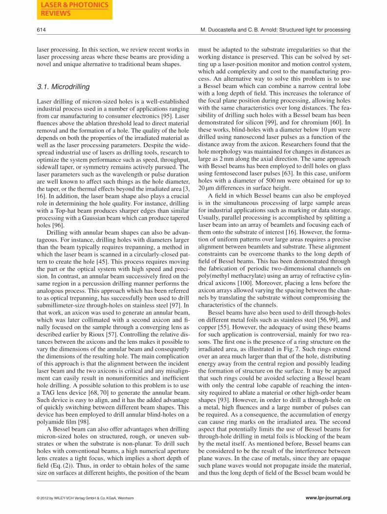
Bessel beams have also been used to drill through-holeson different metal foils such as stainless steel [56, 99], andcopper [55]. However, the adequacy of using these beamsfor such application is controversial, mainly for two rea-sons. The first one is the presence of a ring structure on theirradiated area, as illustrated in Fig. 7. Such rings extendover an area much larger than that of the hole, distributingenergy away from the central region and possibly leadingthe formation of structure on the surface. It may be arguedthat such rings could be avoided selecting a Bessel beamwith only the central lobe capable of reaching the inten-sity required to ablate a material or other high-order beamshapes [93]. However, in order to drill a through-hole ona metal, high fluences and a large number of pulses canbe required. As a consequence, the accumulation of energycan cause ring marks on the irradiated area. The secondaspect that potentially limits the use of Bessel beams forthrough-hole drilling in metal foils is blocking of the beamby the metal itself. As mentioned before, Bessel beams canbe considered to be the result of the interference betweenplane waves. In the case of metals, since they are opaquesuch plane waves would not propagate inside the material,and thus the long depth of field of the Bessel beam would be
© 2012 by WILEY-VCH Verlag GmbH & Co. KGaA, Weinheim www.lpr-journal.org
Laser Photonics Rev. 6, No. 5 (2012)
REVIEWARTICLE
615
Figure 7 Scanning laser microscope images of a hole drilledusing a Bessel beam into a stainless steel sheet with a thicknessof 20 μm. (a) Irradiated surface, with the characteristic marks ofleft by the Bessel rings; (b) rear surface, with a hole smaller thanat the entrance showing tapering [56].
lost. However, if the drilled metal foil is thin enough, holesdrilled with a Bessel beam can exhibit sharper sidewallsand less taper than holes drilled into the same foil using aTop-hat or Gaussian beam [56].
3.2. Fabrication of micro/nano channels intransparent materials
Machining transparent materials with ultrashort laser pulses(shorter than 1 ps) has become a common process for pro-ducing structures within the volume of a material for opticaland photonic applications as well as dicing and cutting [101].Despite the apparent contradiction of using a laser to modifya material that is transparent to that laser wavelength, whenultrafast laser pulses are focused into small spots the intensi-ties achieved in the focal volume are high enough to inducenonlinear absorption, modifying the material properties inthat region [2]. Thus, the material modification is localizedin 3D, whereas the rest of the material remains unaltered.Such spatial confinement, in addition to the translation ofthe laser within the material or other non-linear effects suchas filamentation [102,103], can be used to generate channelsor complex three-dimensional structures.
The use of non-Gaussian beam shapes, with their uniqueproperties, can be beneficial for machining transparent ma-terials in many instances. A situation that illustrates this isthe fabrication of long three-dimensional channels with areduced diameter, which is important for applications suchas microfluidics or for waveguide fabrication. Such channelsare usually obtained with a Gaussian beam and a high NAlens to focus the radiation into a micron-sized spot com-bined with translation of the sample to produce the channel.This requires precise alignment and feedback, which furtherreduces the speed of the process. A Bessel beam introducesa more efficient way to produce such long channels. In thiscase, and contrary to what occurred for opaque materials,the plane waves that form the Bessel beam can propagatethrough the transparent material and provide the beam witha high depth of field within the bulk material. Due to thelocalization of multiphoton absorption to only the narrow
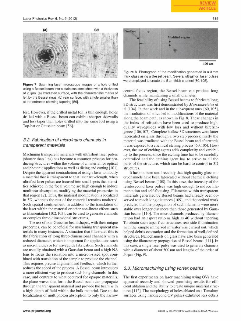
Figure 8 Photograph of the modification generated in a 3 mmthick glass using a Bessel beam. Several ultrashort laser pulseswere employed to create the 5 μm thick channel [60,105].
central focus region, the Bessel beam can produce longchannels while maintaining a small diameter.
The feasibility of using Bessel beams to fabricate long,3D structures was first demonstrated by Marcinkevicius etal [104]. In that work and in the subsequent ones [60, 105],the irradiation of silica led to modifications of the materialalong the beam path, as shown in Fig. 8. These changes inthe index of refraction have been used to produce high-quality waveguides with low loss and without birefrin-gence [106,107]. Complete hollow 3D structures were latterfabricated on glass through a two step process: firstly thematerial was irradiated with the Bessel beam and afterwardsit was exposed to a chemical etching process [60,105]. How-ever, the use of etching agents adds complexity and variabil-ity to the process, since the etching time has to be carefullycontrolled and the etching agent has to arrive to all theparts of the structure, which can be hard to control in 3Dstructures.
It has not been until recently that high quality glass mi-crochannels have been fabricated without chemical etchingusing Bessel beams [108]. In this case, the intensity of thefemtosecond laser pulses was high enough to induce fila-mentation and self-focusing. Filaments within transparentmaterials generated by Bessel beams had already been ob-served to reach long distances [109], and theoretical workpredicted that the propagation of such filaments were morestable over longer distances than those generated by Gaus-sian beams [110]. The microchannels produced by filamen-tation had an aspect ratio as high as 40 without tapering.To obtain such taper free structures rear-side illuminationwith the sample immersed in water was carried out, whichhelped debris evacuation and the formation of well-definedstructures. Nanochannels on glass have also been generatedusing the filamentary propagation of Bessel beams [111]. Inthis case, a single laser pulse was used to generate channelswith a diameter of about 500 nm and lengths of the order of50 μm (Fig. 9).
3.3. Micromachining using vortex beams
The first experiments on laser machining using OVs haveappeared recently and showed promising results for effi-cient ablation and the ability to create unique material struc-tures [112]. The morphology of holes ablated on a Tantalumsurfaces using nanosecond OV pulses exhibited less debris
www.lpr-journal.org © 2012 by WILEY-VCH Verlag GmbH & Co. KGaA, Weinheim

616
LASER & PHOTONICSREVIEWS
M. Duocastella and C. B. Arnold: Structured light for processing
Figure 9 SEM image of a chan-nel generated in glass using a singleshot from a Bessel beam. The inten-sity of the femtosecond pulse was highenough to induce filamentation [111].
Figure 10 SEM images of ablation rings on soda-lime glassproduced with single femtosecond vortex pulses. (a) Ablation en-ergies of 100, 150, 250, and 700 nJ, from left to right. (b) Cavitieson the beam axis, where the intensity is negligible, produced atan energy of about 1.5 μJ. (c) 200 μm x 200 μm array producedat an energy of 250 nJ, which demonstrates the reproducibility ofthe ablation process [50].
and a better definition than those processed using annularbeams without orbital angular momentum (OAM). By us-ing circularly polarized light in combination with the OV,it becomes possible to create microneedles in the centralregion of the ablated spot without affecting the surroundingmaterial.
Femtosecond vortex pulses can also lead to the modifica-tion of material in the center of the annular intensity profile,as demonstrated by irradiating soda-lime glass [50]. Fem-tosecond OV pulses with fluences slightly above the ablationthreshold resulted in reproducible annular holes with cleanedges. As the fluence was increased, deep cavities started toform in the annulus center where the residual light was neg-ligible (Fig. 10). The formation of these cavities has beenattributed to a toroidal plasma induced by high-intensityvortex pulses [50]. The expansion of such torodial plasmaproduces two shock waves: one that propagates towards thesurrounding material and one to the annulus center. Thissecond one would produce a dramatic rise in pressure whenreaching the annulus center and leads to material removal.Therefore, from the previous examples it can be concludedthat OVs induce very particular light-matter interactions thatcould be advantageous in several laser processing applica-tions.
3.4. Nanopatterning
The processing of materials on the nanoscale is a growingdemand in several areas, including electronics [113] and
biotechnology [114]. The diffraction limit of conventionalfocusing optics has traditionally restricted the use of opticaltechniques to micron and sub-micron size scales. However,recent strategies have been developed to overcome this limit.Apart from the previously mentioned multiphoton absorp-tion, near-field effects can similarly overcome traditionaldiffraction limitations to produce nanoscale features [115].This takes the advantage of evanescent waves near interfacesand surfaces, usually generated after irradiating a particleor near-field objective with a laser beam, to allow an en-hancement of the electric field in a confined region closeto the particle surface. Arrays of dielectric microbeads canbe self-assembled on a surface [116, 117] and a single laserpulse can be used to create a corresponding array of isolateddots or other shapes [118–120].
However, in order to harness the near-field intensifica-tion of light for user defined nanopatterns, it is necessary tomanipulate the near-field objective along the surface whileaccurately maintaining a separation of 10’s of nm from theworkpiece surface. It is possible to do this by taking advan-tage of the “nondiffracting” behavior of Bessel beams foroptical trapping. Contrary to conventional optical traps usingGaussian beams, Bessel beam traps only exhibit significantgradients in the transverse directions, which leads to particleconfinement in two dimensions with a scattering force inthe propagation direction [121]. This scattering force canbe balanced by the interaction forces between the particleand surface, such as Van der Waals, seteric and electrostaticrepulsion, resulting in an equilibrium distance between par-ticle and surface on the order of 50 nm depending on thetrapping laser intensity and system chemistry [122]. There-fore, the use of Bessel beams enables the self-positioningof the particle relative to the substrate regardless of sur-face inhomogeneities and without the requirement of feed-back control. As a consequence, if the trapped particle isirradiated with a second laser pulse so that the near-fieldeffects induced enable the modification of the workpiecesurface, it is possible to controllably generate nanofeatures.The feasibility of this technique, called optical trap assistednanopatterning (OTAN), has been demonstrated through thecreation of various types of surface modifications, includingbumps, pits and holes, depending on the material and thepulsed laser fluence [121] (Fig. 11), the implementation ofparallel nanopatterning [123], and even the ability to tra-verse rough and textured surfaces [124, 125]. The minimumfeature sizes were 100 nm, and the positioning accuracy wasbetter than 40 nm.
3.5. Photopolymerization
Photopolymerization using laser beams is a well knownprototyping technique that can be used to fabricate micro
© 2012 by WILEY-VCH Verlag GmbH & Co. KGaA, Weinheim www.lpr-journal.org

Laser Photonics Rev. 6, No. 5 (2012)
REVIEWARTICLE
617
Figure 11 (online color at: www.lpr-journal.org) SEM images illustrating the ability to parallel processing using OTAN. (a) Four P’swritten using overlapping laser pulses with10 mJ/cm2 incident fluence. (b) Overlaid image of the four P’s in (a). (c) Four O’s writtenusing 12 mJ/cm2 fluence, and particles of different sizes (0.75 μm upper-right, 3 μm lower-right, 2 μm the other two). This illustrates thecapability to simultaneously produce different line widths in an array. (d) Four test patterns of individual shots used to test positioningaccuracy and feature size uniformity (incident fluence is 15 mJ/cm2). (e) The overlaid image of the four patterns in (d), illustrating theidentical nature of the patterns. (f) Forces acting on the microsphere that maintain its position relative to the substrate without anyfeedback control. The scale bar in (b) is 500 nm, all other scale bars are 2 mm long [123].
and nanostructures [126, 127]. In this technique, a laserbeam is scanned along a liquid photoresist to induce cross-linking. After exposure, the photoresist is developed, leadingto microstructures in the areas the photoresist was exposed.Traditionally, polymerization has been performed with CWultraviolet lasers over surfaces, which results in 2D struc-tures [128]. More recently, complex 3D structures have beenobtained with CW [129, 130] and picosecond lasers [131]by confining the photopolymerized region to the beam fo-cal volume and then moving it with respect to the sample.This approach makes use of the threshold behavior of pho-toresists, which prevents any modification below a certainoptical intensity. Alternatively, ultrafast lasers, taking ad-vantage of multiphoton absorption, have been employed forphotopolymerization [132]. In this case, the material modifi-cation can be much easily confined within the focal volumeof the beam. Once again, by controlling the intensity ofthe Gaussian beam, the non-linear absorption allows one toovercome the diffraction limit [133] and produce structureswith a nanometer resolution [134, 135].
The use of non-conventional beam shapes confers somebenefits in photopolymerization as well. Again, the longdepth of field of Bessel beams can be used to fabricatelong structures without the need to translate a sample. Thishas been demonstrated through the fabrication of homo-geneous polymer fibers using a CW laser with a Besselbeam [136]. Fibers as long as 15 mm, with a diameter below5 μm (Fig. 12) have been fabricated through this approach.The length of the fiber greatly exceeded the maximal prop-agation distance that a Bessel beam should attain withinthe fluid used, due to waveguiding provided by the fiber
Figure 12 ESEM images of the left (a), middle (b) and right (c)parts of a polymer fiber with a length of 15 mm. The fiber wascreated illuminating a liquid photopolymer with a Bessel beamfrom a CW laser [136].
itself as it formed, a structure termed “self-written wave-guide” [137]. Bessel beams have also been employed inthe fabrication of 3D structures using multiphoton polymer-ization and scanning the beam through the volume of thesample [138, 139].
Annular beams can be used with polymerization todirectly generate circles and related structures withoutthe need for translation stages and their related prob-lems [58,140]. Moreover, translating the sample in the threedirections of space in a step-and-repeat way allowed theannular patterns to be stacked into larger structures, as pre-sented in Fig. 13.
Another important application of annular beams in pho-topolymerization is to enhance the resolution to sub 50 nm.Analogous to the STED microscopy technique [64], an an-nular beam used to deactivate the polymerization can beoverlapped with a Gaussian beam that induces polymer-ization. Thus, the effective polymerization voxel would beconfined in the center of the annulus. Reducing the dimen-sions of the annular center results in a smaller spot by furtherlimiting the polymerization reaction above and beyond the
www.lpr-journal.org © 2012 by WILEY-VCH Verlag GmbH & Co. KGaA, Weinheim

618
LASER & PHOTONICSREVIEWS
M. Duocastella and C. B. Arnold: Structured light for processing
Figure 13 SEM images of complex patterns generated by 2 pho-ton polymerization using an annular beam. The irradiated materialhad a low absorption cross section at the laser wavelength, andonly at the focal region the beam intensity was high enough toproduce photopolymerization through non-linear absorption pro-cesses. Translating the laser beam allowed the formation of (a)2D and (b) 3D structures [138].
multiphoton effects. The combination of initiation and deac-tivation beams in polymerization has already demonstrateda resolution in the direction of the incident beam of λ /20and further refinement continues to push the feature sizesmaller [141, 142].
4. Conclusions and outlook
We have presented a review of recent work in the processingof materials using Bessel and annular beams, as well as adiscussion of the properties and generation methods for suchstructured illumination. Considering these aspects, it canbe concluded that the use of shaped beams can be a scien-tifically interesting and technologically relevant alternativeto conventional Gaussian and Top-hat beams for many ap-plications. For instance, the “non-diffracting” behavior ofBessel beams results in a long depth of field, which can beused to increase the tolerance of the focal plane positionduring material processing. This allows the creation of uni-form features over non-planar or uneven surfaces withoutthe need to adjust the relative position of the sample andfocus as with shorter depth of field beams. Such long depthof field also makes Bessel beams suitable to produce highaspect ratio structures, such as long channels in transpar-ent materials or polymerized fibers, without scanning thebeam inside the material or otherwise translating the sample.Similarly, annular beams have advantages for creating novelstructures in materials, improved micromachining and deep-hole drilling, and reducing the feature size in multiphotonpolymerization. Furthermore, the related vortex beams caninduce unique light-matter interactions leading to enhancedablative processing.
The role of laser beam shaping for scientific and indus-trial applications is expanding, increasing the breadth andcapabilities of laser based materials processing. Novel andcost-effective methods to generate these structured beamshave opened a new chapter in fundamental laser-matter in-teractions, enabling unique material responses with controldown to the nanoscale, and have the potential to revolution-ize the way lasers are used for processing. As we learn moreabout structured optical fields, their effect on materials, and
new methods to tailor light properties, interesting possibili-ties will continue to emerge, providing fruitful opportunitiesfor process development and optimization.
Acknowledgements. The authors acknowledge financial supportfrom AFOSR and NSF, as well as useful conversations with Dr. M.Brown, Dr. S. Ramachandran, and Dr. A. Rode on aspects of thismanuscript.
Received: 21 June 2011, Revised: 23 August 2011,Accepted: 5 October 2011
Published online: 17 January 2012
Key words: Bessel beam, annular beam, optical vortex, ma-terials processing, nanopatterning, photopolymerization, non-diffracting beam.
Marti Duocastella studied physics at theUniversity of Barcelona, where he ob-tained his Ph. D. in physics in 2010 onthe study of the fundamentals of a laserprinting technique for the fabrication ofbiosensors. He is currently a postdoctoralfellow at Princeton University. His currentresearch involves the study of adaptiveoptics systems for laser processing andimaging applications.
Craig B. Arnold is an associate pro-fessor at Princeton University in the de-partment of Mechanical and AerospaceEngineering and the Princeton Institutefor Science and Technology of Materi-als (PRISM). His research interests in-volves laser processing and transport inmaterials with particular efforts in adap-tive optics, laser based nanopatterning,and laser direct write technologies. He
currently serves as the Associate Academic Director of PRISMand as the Princeton IGERT Director on Nanotechnology forClean Energy.
References
[1] J. Wilson and J. F. B. Hawkes (eds.), Laser principles and
applications (Prentice Hall International, Hertfordshire, UK,
1987).
[2] M. Brown and C. B. Arnold, in: Laser precision microfab-
rication, edited by K. Sugioka, M. Meunier, and A. Pique
(Springer-Verlag, Berlin, 2010).
[3] W. M. Steen (ed.), Laser Materials Processing (Springer,
London, 1991).
[4] S. P. H. Narendra and B. Dahotre (eds.), Laser fabrica-
tion and machining of materials (Springer, New York, NY,
2008).
[5] W. Dudley (ed.), Laser Processing and Analysis of Materials
(Plenum Press, New York, USA, 1983).
© 2012 by WILEY-VCH Verlag GmbH & Co. KGaA, Weinheim www.lpr-journal.org
Laser Photonics Rev. 6, No. 5 (2012)
REVIEWARTICLE
619
[6] E. Kannatey-Asibu (ed.), Principles of Laser Materials Pro-
cessing (John Wiley & Sons, Inc., Hoboken, New Jersey,
2009).[7] C. P. Grigoropoulos, S.-J. Moon, and M.-H. Lee, in: Laser
Crystallization of Silicon-Fundamentals to Devices, edited
by N. H. Nickel (Elsevier, Berlin, Germany, 2003), Chap. 2.[8] G. Olivie, D. Giguere, F. Vidal, T. Ozaki, J. C. Kieffer,
O. Nada, and I. Brunette, Opt. Express 16, 4121 (2008).[9] C. Hnatovsky, V. Shvedov, W. Krolikowski, and A. Rode,
Phys. Rev. Lett. 106, 123901 (2011).[10] V. G. Niziev and A. V. Nesterov, J. Phys. D, Appl. Phys. 32,
1455 (1999).[11] J. P. Colombier, P. Combis, A. Rosenfeld, I. V. Hertel, E. Au-
douard, and R. Stoian, Phy. Rev. B 74, 224106 (2006).[12] B. N. Chichkov, C. Momma, S. Nolte, F. v. Alvensleben,
and A. Tunnermann, Appl. Phys. A, Mater. 63, 109 (1996).[13] F. M. Dickey and S. C. Holswade (eds.), Laser beam shap-
ing, theory and techniques (Marcel Dekker, New York, NY,
2000).[14] R. Paschotta (ed.), Encyclopedia of laser physics and tech-
nology (Wiley-VCH, Weinheim; Chichester, 2008).[15] K. Venkatakrishnan, B. Tan, L. H. K. Koh, and
B. K. A. Ngoi, Opt. Laser Eng. 38, 425 (2002).[16] J. C. Ion (ed.), Laser processing of engineering materials:
principles, procedure, and industrial application (Elsevier-
Butterworth-Heinemann, Burlington, MA, 2005).[17] A. E. Siegman (ed.), Lasers (University Science Books, Mill
Valley, CA, 1986).[18] H. Helvajian, in: Direct-write technologies for rapid proto-
typing applications, edited by A. Pique and D. B. Chriesy
(Academic Press, San Diego, CA, 2002), Chap. 14.[19] M. Miyasaka and J. Stoemenos, J. Appl. Phys. 86, 5556
(1999).[20] D. B. Chrisey and G. K. Hubler (eds.), Pulsed laser deposi-
tion of thin films (J. Wiley, New York, 1994).[21] K. Washio, in: Laser precision microfabrication, edited by
K. Sugioka, M. Meunier, and A. Pique (Springer-Verlag,
Berlin, 2010), Chap. 3.[22] K. Jain (ed.), Excimer laser lithography (SPIE Optical En-
gineering Press, Bellingham, Wash., USA, 1990).[23] A. Masters and T. Geuking, Laser focus world 41 (2005).[24] C. B. Arnold, P. Serra, and A. Pique, Mrs Bulletin 32, 23
(2007).[25] M. Colina, M. Duocastella, J. M. Fernandez-Pradas, P. Serra,
and J. L. Morenza, J. Appl. Phys. 99 (2006).[26] M. S. Brown, N. T. Kattamis, and C. B. Arnold, J. Appl.
Phys. 107 (2010).[27] R. Auyeung, H. Kim, N. Charipar, A. Birnbaum, S. Math-
ews, and A. Pique, Appl. Phys. A, Mater., DOI:
10.1007/s00339 (2010).[28] V. Garces-Chavez, D. McGloin, H. Melville, W. Sibbett,
and K. Dholakia, Nature 419, 145 (2002).[29] K. Dholakia and W. M. Lee, in: Advances in Atomic, Molec-
ular, and Optical Physics, Vol. 56, edited by E. Arimondo,
P. R. Berman, and C. C. Lin (Academic Press, Burlington,
MA, 2008), pp. 261–337.[30] V. G. Shvedov, A. V. Rode, Y. V. Izdebskaya, A. S. Desyat-
nikov, W. Krolikowski, and Y. S. Kivshar, Phys. Rev. Lett.
105, 118103 (2010).[31] J. Arlt, T. Hitomi, and K. Dholakia, Appl. Phys. B, Laser O.
71, 549 (2000).[32] M. Padgett, J. Courtial, and L. Allen, Phys. Today 57, 35
(2004).
[33] G. Molina-Terriza, J. P. Torres, and L. Torner, Nat. Phys. 3,
305 (2007).
[34] M. Mazilu, D. Stevenson, F. Gunn-Moore, and K. Dholakia,
Laser Photonics Rev. 4, 529 (2010).
[35] N. Blow, Nature 456, 825 (2008).
[36] S. W. Hell, Nat. Methods 6, 24 (2009).
[37] X. Tsampoula, V. Garces-Chavez, M. Comrie, D. J. Steven-
son, B. Agate, C. T. A. Brown, F. Gunn-Moore, and K. Dho-
lakia, Appl. Phys. Lett. 91, 053902 (2007).
[38] X. Tsampoula, K. Taguchi, T. Cizmar, V. Garces-Chavez,
N. Ma, S. Mohanty, K. Mohanty, F. Gunn-Moore, and
K. Dholakia, Opt. Express 16, 17007 (2008).
[39] D. McGloin and K. Dholakia, Contemp. Phys. 46, 15
(2005).
[40] L. Allen, M. W. Beijersbergen, R. J. C. Spreeuw, and
J. P. Woerdman, Phys. Rev. A 45, 8185 (1992).
[41] A. Bekshaev, K. Y. Bliokh, and M. Soskin, J. Opt. 13,
053001 (2011).
[42] D. L. Andrews (ed.), Structured light and its applications
(Elsevier: Academic Press, Amsterdam, 2008).
[43] T. Watanabe, M. Fujii, Y. Watanabe, N. Toyama, and Y. Ike-
taki, Rev. Sci. Instrum. 75, 5131 (2004).
[44] D. Ganic, X. Gan, M. Gu, M. Hain, S. Somalingam,
S. Stankovic, and T. Tschudi, Opt. Lett. 27, 1351 (2002).
[45] D. Zeng, W. P. Latham, and A. Kar, J. Laser Appl. 17, 256
(2005).
[46] J. Durnin, J. J. Miceli, and J. H. Eberly, Phys. Rev. Lett. 66,
838 (1991).
[47] P. Polesana, D. Faccio, P. Di Trapani, A. Dubietis,
A. Piskarskas, A. Couairon, and M. A. Porras, Opt. Express
13, 6160 (2005).
[48] J. Durnin, J. J. Miceli, and J. H. Eberly, Phys. Rev. Lett. 58,
1499 (1987).
[49] M. A. Sheikh and L. Li, P. I. Mech. Eng. C, J. Mec. 224,
1061 (2010).
[50] C. Hnatovsky, V. G. Shvedov, W. Krolikowski, and
A. V. Rode, Opt. Lett. 35, 3417 (2010).
[51] S. Safdar, L. Li, M. A. Sheikh, and L. Zhu, Opt. Laser
Technol. 39, 1101 (2007).
[52] J. W. Goodman (ed.), Introduction to Fourier optics
(Roberts, Englewood, Colorado, 2005).
[53] J. H. McLeod, J. Opt. Soc. Am. 44, 592 (1954).
[54] G. Roy and R. Tremblay, Opt. Commun. 34, 1 (1980).
[55] I. Alexeev, K. H. Leitz, A. Otto, and M. Schmidt, Phys.
Procedia 5, 533 (2010).
[56] Y. Matsuoka, Y. Kizuka, and T. Inoue, Appl. Phys. A, Mater.
84, 423 (2006).
[57] M. Rioux, R. Tremblay, and P. A. Belanger, Appl. Opt. 17,
1532 (1978).
[58] R. J. Winfield, B. Bhuian, S. O’Brien, and G. M. Crean,
Appl. Phys. Lett. 90, 111115 (2007).
[59] G. Milne, G. D. M. Jeffries, and D. T. Chiu, Appl. Phys. Lett.
92, 261101 (2008).
[60] J. Amako, K. Yoshimura, D. Sawaki, and T. Shimoda, Pro-
ceedings SPIE 5713, 497 (2005).
[61] U. Efron (ed.), Spatial light modulator technology: materi-
als, devices, and applications (Marcel Dekker, New York,
1995).
[62] C. Maurer, A. Jesacher, S. Bernet, and M. Ritsch-Marte,
Laser Photonics Rev. 5, 81 (2011).
[63] F. Courvoisier, P. A. Lacourt, M. Jacquot, M. K. Bhuyan,
L. Furfaro, and J. M. Dudley, Opt. Lett. 34, 3163 (2009).
www.lpr-journal.org © 2012 by WILEY-VCH Verlag GmbH & Co. KGaA, Weinheim

620
LASER & PHOTONICSREVIEWS
M. Duocastella and C. B. Arnold: Structured light for processing
[64] K. I. Willig, B. Harke, R. Medda, and S. W. Hell, Nat Meth
4, 915 (2007).
[65] J. A. Davis, E. Carcole, and D. M. Cottrell, Appl. Opt. 35,
599 (1996).
[66] A. M. Weiner, Rev. Sci. Instrum. 71, 1929 (2000).
[67] R. J. Beck, J. P. Parry, W. N. MacPherson, A. Waddie,
N. J. Weston, J. D. Shephard, and D. P. Hand, Opt. Express
18, 17059 (2010).
[68] E. McLeod, A. B. Hopkins, and C. B. Arnold, Opt. Lett. 31,
3155 (2006).
[69] K. A. Higginson, M. A. Costolo, and E. A. Rietman, Appl.
Phys. Lett. 84, 843 (2004).
[70] C. B. Arnold and E. McLeod, Photon. Spectra 41, 78 (2007).
[71] E. McLeod and C. B. Arnold, J. Appl. Phys. 102, 033104:1–
9 (2007).
[72] E. McLeod and C. B. Arnold, Appl. Opt. 47, 3609 (2008).
[73] A. Mermillod-Blondin, E. McLeod, and C. B. Arnold, Opt.
Lett. 33, 2146 (2008).
[74] N. Olivier, A. Mermillod-Blondin, C. B. Arnold, and
E. Beaurepaire, Opt. Lett. 34, 1684 (2009).
[75] A. Mermillod-Blondin, E. McLeod, and C. B. Arnold, Appl.
Phys. A, Mater. 93, 231 (2008).
[76] M. Duocastella and C. B. Arnold, to be published (2011).
[77] F. W. Wise, A. Chong, and W. H. Renninger, Laser Photon-
ics Rev. 2, 58 (2008).
[78] S.-K. Eah, W. Jhe, and Y. Arakawa, Rev.Sci. Instr. 74, 4969
(2003).
[79] K. M. Tan, M. Mazilu, T. H. Chow, W. M. Lee, K. Taguchi,
B. K. Ng, W. Sibbett, C. S. Herrington, C. T. A. Brown, and
K. Dholakia, Opt. Express 17, 2375 (2009).
[80] T. Grosjean, S. S. Saleh, M. A. Suarez, I. A. Ibrahim, V. Pi-
querey, D. Charraut, and P. Sandoz, Appl. Opt. 46, 8061
(2007).
[81] J. K. Kim, J. Kim, Y. Jung, W. Ha, Y. S. Jeong, S. Lee,
A. Tunnermann, and K. Oh, Opt. Lett. 34, 2973 (2009).
[82] X. Zhu, A. Schulzgen, L. Li, and N. Peyghambarian, Appl.
Phys. Lett. 94, 201102 (2009).
[83] S. R. Lee, J. Kim, S. Lee, Y. Jung, J. K. Kim, and K. Oh,
Opt. Express 18, 25299 (2010).
[84] S. Ramachandran, J. W. Nicholson, S. Ghalmi, M. F. Yan,
P. Wisk, E. Monberg, and F. V. Dimarcello, Opt. Lett. 31,
1797 (2006).
[85] S. Ramachandran, J. M. Fini, M. Mermelstein, J. W. Nichol-
son, S. Ghalmi, and M. F. Yan, Laser Photonics Rev. 2, 429
(2008).
[86] R. Siddharth and G. Samir, in: Proceedings of the Confer-
ence on Lasers and Electro-Optics/Quantum Electronics
and Laser Science Conference and Photonic Applications
Systems Technologies (Optical Society of America, San
Jose, CA, 2008), paper CPDB5.
[87] J. Yin, H.-R. Noh, K.-I. Lee, K.-H. Kim, Y.-Z. Wang, and
W. Jhe, Opt. Commun. 138, 287 (1997).
[88] H. Ma, H. Cheng, W. Zhang, L. Liu, and Y. Wang, Chin.
Opt. Lett. 5, 460 (2007).
[89] C. Zhao, Y. Cai, F. Wang, X. Lu, and Y. Wang, Opt. Lett.
33, 1389 (2008).
[90] A. Vasara, J. Turunen, and A. T. Friberg, J. Opt. Soc. Am.
A 6, 1748 (1989).
[91] W.-X. Cong, N.-X. Chen, and B.-Y. Gu, J. Opt. Soc. Am. A
15, 2362 (1998).
[92] T. A. Klar, S. Jakobs, M. Dyba, A. Egner, and S. W. Hell,
Proc. Natl. Acad. Sci. USA 97, 8206 (2000).
[93] K. Sueda, G. Miyaji, N. Miyanaga, and M. Nakatsuka, Opt.
Express 12, 3548 (2004).
[94] V. G. Shvedov, C. Hnatovsky, W. Krolikowski, and
A. V. Rode, Opt. Lett. 35, 2660 (2010).
[95] O. Suttmann, A. Moalem, R. Kling, and A. Ostendorf, in:
Laser precision microfabrication, edited by K. Sugioka,
M. Meunier, and A. Pique (Springer-Verlag, Berlin, 2010),
Chap. 13.
[96] N. Sanner, N. Huot, E. Audouard, C. Larat, and J. P. Huig-
nard, Opt. Laser Eng. 45, 737 (2007).
[97] D. Zeng, W. P. Latham, and A. Kar, Proceedings of SPIE
6290, 62900J (2006).
[98] A. Mermillod-Blondin, E. McLeod, and C. B. Arnold, Appl.
Phys. A, Mater. 93, 231 (2008).
[99] M. Kohno and Y. Matsuoka, JSME. Int. J. B, Fluid. T. 47,
497 (2004).
[100] R. Grunwald, U. Neumann, A. Rosenfeld, J. Li, and
P. R. Herman, Opt. Lett. 31, 1666 (2006).
[101] R. R. Gattass and E. Mazur, Nat. Photon. 2, 219 (2008).
[102] A. Couairon and A. Mysyrowicz, Phys. Rep. 441, 47 (2007).
[103] Y. Hayasaki, M. Isaka, A. Takita, and S. Juodkazis, Opt.
Express 19, 5725 (2011).
[104] A. Marcinkevicius, S. Juodkazis, S. Matsuo, V. Mizeikis,
and H. Misawa, Jpn. J. Appl. Phys. 2 40, L1197 (2001).
[105] J. Amako, D. Sawaki, and E. Fujii, J. Opt. Soc. Am. B, Opt.
Phys. 20, 2562 (2003).
[106] Z. Veronique, M. Nathalie, and P. Michel, Proceedings SPIE
7099, 70992J (2008).
[107] Z. Veronique, M. Nathalie, and P. Michel, Proceedings SPIE
7386, 738632 (2009).
[108] M. K. Bhuyan, F. Courvoisier, P. A. Lacourt, M. Jacquot,
L. Furfaro, M. J. Withford, and J. M. Dudley, Opt. Express
18, 566 (2010).
[109] E. Gaizauskas, E. Vanagas, V. Jarutis, S. Juodkazis,
V. Mizeikis, and H. Misawa, Opt. Lett. 31, 80 (2006).
[110] P. Polesana, M. Franco, A. Couairon, D. Faccio, and
P. Di Trapani, Phys. Rev. A 77, 043814 (2008).
[111] M. K. Bhuyan, F. Courvoisier, P. A. Lacourt, M. Jacquot,
R. Salut, L. Furfaro, and J. M. Dudley, Appl. Phys. Lett. 97,
081102 (2010).
[112] J. Hamazaki, R. Morita, K. Chujo, Y. Kobayashi, S. Tanda,
and T. Omatsu, Opt. Express 18, 2144 (2010).
[113] D. Appell, Nature 419, 553 (2002).
[114] M. C. Roco, Curr. Opin. Biotechnol. 14, 337 (2003).
[115] E. Betzig and J. K. Trautman, Science 257, 189 (1992).
[116] S. M. Huang, M. H. Hong, B. Lukiyanchuk, and T. C. Chong,
Appl. Phys. A, Mater. 77, 293 (2003).
[117] Y. Hsiharng, C.-K. Chao, M.-K. Wei, and C.-P. Lin, J. Mi-
cromech. Microeng. 14, 1197 (2004).
[118] Y. Lin, M. H. Hong, T. C. Chong, C. S. Lim, G. X. Chen,
L. S. Tan, Z. B. Wang, and L. P. Shi, Appl. Phys. Lett. 89,
041108 (2006).
[119] Y. Zhou, M. H. Hong, J. Y. H. Fuh, L. Lu, and B. S. Luk,
’yanchuk, Z. B. Wang, L. P. Shi, and T. C. Chong, Appl.
Phys. Lett. 88, 023110 (2006).
[120] W. Wu, A. Katsnelson, O. G. Memis, and H. Mohseni, Nan-
otechnology 18, 485302 (2007).
[121] E. McLeod and C. B. Arnold, Nat. Nanotechnol. 3, 413
(2008).
[122] R. Fardel, E. McLeod, Y.-C. Tsai, and C. Arnold, Appl.
Phys. A, Mater 101, 41 (2010).
[123] E. McLeod and C. B. Arnold, Opt. Express 17, 3640 (2009).
© 2012 by WILEY-VCH Verlag GmbH & Co. KGaA, Weinheim www.lpr-journal.org
Laser Photonics Rev. 6, No. 5 (2012)
REVIEWARTICLE
621
[124] Y.-C. Tsai, R. Fardel, and C. B. Arnold, AIP Conf. Proc.
1278, 457 (2010).[125] Y. C. Tsai, R. Fardel, and C. B. Arnold, Appl. Phys. Lett.
98, 233110 (2011).[126] R. Nassar and W. Dai (eds.), Modelling of microfabrication
systems (Springer-Verlag, Berlin, 2003).[127] S. Maruo and J. T. Fourkas, Laser Photonics Rev. 2, 100
(2008).[128] C. Decker, in: L. F. Thompson, C. G. Willson, and
J. M. J. Frechet (eds.), Materials for Microlithography
Radiation-Sensitive Polymers (American Chemical Society,
Washington, 1985), Chap. 9.[129] S. Maruo and K. Ikuta, Appl. Phys. Lett. 76, 2656 (2000).[130] M. Thiel, J. Fischer, G. v. Freymann, and M. Wegener, Appl.
Phys. Lett. 97, 221102 (2010).[131] M. Malinauskas, P. Danilevicius, and S. Juodkazis, Opt.
Express 19, 5602 (2011).[132] S. Maruo, O. Nakamura, and S. Kawata, Opt. Lett. 22, 132
(1997).[133] S. Kawata, H.-B. Sun, T. Tanaka, and K. Takada, Nature
412, 697 (2001).
[134] L. Li, E. Gershgoren, G. Kumi, W.-Y. Chen, P. T. Ho,
W. N. Herman, and J. T. Fourkas, Adv. Mater. 20, 3668
(2008).
[135] M. Farsari and B. N. Chichkov, Nat Photon 3, 450 (2009).
[136] J. Jezek, T. Cizmar, V. Nedela, and P. Zemanek, Opt. Ex-
press 14, 8506 (2006).
[137] S. J. Frisken, Opt. Lett. 18, 1035 (1993).
[138] X. F. Li, R. J. Winfield, S. O’Brien, and G. M. Crean, Appl.
Surf. Sci. 255, 5146 (2009).
[139] C. F. Phelan, R. J. Winfield, D. P. O’Dwyer, Y. P. Rakovich,
J. F. Donegan, and J. G. Lunney, Opt. Commun. 284, 3571
(2011).
[140] B. Bhuian, R. J. Winfield, S. O’Brien, and G. M. Crean,
Appl. Surf. Sci. 254, 841 (2007).
[141] L. Li, R. R. Gattass, E. Gershgoren, H. Hwang, and
J. T. Fourkas, Science 324, 910 (2009).
[142] M. P. Stocker, L. Li, R. R. Gattass, and J. T. Fourkas, Nat.
Chem. 3, 223 (2011).
www.lpr-journal.org © 2012 by WILEY-VCH Verlag GmbH & Co. KGaA, Weinheim