Embed Size (px)
Citation preview
BESI
Semi Packaging Tech Seminar June 18th , Vila do Conde - Portugal

Agenda
2
Company Overview
Equipment portfolio
Market
Process and package Roadmap

€ 85.5
€ 378.8
25.9%
43.8%
20%
25%
30%
35%
40%
45%
0
100
200
300
400
2003 2014
Gro
ss M
arg
in (
%)
Reven
ue
(€
mill
ion
s)
Revenue Gross Margin
Company History – Founded in 1956
•2000 2002 2005 2009
Die Attach Acquisitions
•2006 Dragon I complete: € 6 million cost savings
•2008 Dragon II complete: € 15 million cost savings
•2010 Plan: € 7.0 million cost savings. Headcount and product line restructuring
•2012 : € 8.3 million cost savings. Headcount reduction. Plating unit rationalized
•2014: US die sorting operations rationalized. Transferred to Besi Austria
Restructuring
•2006-09 Standard packaging and certain die bonding systems transferred to Malaysia
•2007-09 Dutch tooling & Hungarian die bonding transferred to Asia
•2009-11 Epoxy DB transferred to Malaysia
•2003-12 Malaysian system and Chinese tooling capacity expansion.
•2013 Soft solder DB transferred to Malaysia
•2006-14 Asian headcount increased from 34% to 59%
•2015: Transfer of certain software engineering, logistics and related administrative functions from Switzerland to Singapore
Asian Production Transfer
3

Global Operations
as of 31 December 2014
Europe/NA Asia
Revenue (MMs) € 123.4 32.6% € 255.3 67.4%
Headcount 663 40.6% 969 59.4%
• Development/innovation in Europe
• Increasing engineering, production and
logistics activities in Asia
Sales Office
Production Site
Sales & Production Site
* R&D Site
Leshan
Chengdu Shanghai
Korea
Taiwan
Philippines Malaysia
Singapore*
Suzhou
Radfeld, (Austria)* Cham,
(Switzerland)*
Duiven & Drunen,
(The Netherlands)*
Chandler
Shenzhen
4
Salem

22/06/2015
VLSI Research April 21’15:
“BE Semiconductor achieves highest growth (56%) among top assembly equipment
suppliers”
5 #
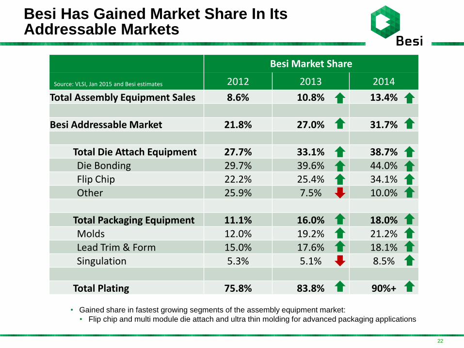
Besi Has Gained Market Share In Its Addressable Markets
• Gained share in fastest growing segments of the assembly equipment market:
• Flip chip and multi module die attach and ultra thin molding for advanced packaging applications
Besi Market Share
Source: VLSI, Jan 2015 and Besi estimates 2012 2013 2014
Total Assembly Equipment Sales 8.6% 10.8% 13.4% Besi Addressable Market 21.8% 27.0% 31.7%
Total Die Attach Equipment 27.7% 33.1% 38.7% Die Bonding 29.7% 39.6% 44.0% Flip Chip 22.2% 25.4% 34.1% Other 25.9% 7.5% 10.0%
Total Packaging Equipment 11.1% 16.0% 18.0% Molds 12.0% 19.2% 21.2% Lead Trim & Form 15.0% 17.6% 18.1% Singulation 5.3% 5.1% 8.5%
Total Plating 75.8% 83.8% 90%+
22

Agenda
7
Company Overview
Equipment portfolio
Market
Process and package Roadmap

Best in Class Product Portfolio
• Molding - AMS series - AMS LM 95 - MMS series - FML
• Die Bonding - 2100 xPplus
- 2100 sDplus - 2100 sD PPPplus
- 2100 HS
- 2009 SSI - 2100 DS
Die Attach Packaging & Plating
• Multi Module Die
Attach - 2200 evo - 2200 evo plus
• Flip Chip - 8800 FC QUANTUM - 8800 CHAMEO - 8800 TCB - 2100 FC
• Trim & Form - Compact series - Power series - Compact Line XHD New
• Plating - Leadframe - Solar - Film & Foil
In Development
•Next generation Die Attach
•Next generation Packaging
•Common modules
Datacon
Datacon
Esec
Fico
Meco
Fico
New
8
Fico
• Singulation
- FSL
- FSL (shield cut)
New
New
• Die Sorting & Special - DS 9000 TRDS - DS WTT - TTR - DLA
Datacon
New
New
New
New
New
Agenda
9
Company Overview
Equipment portfolio
Market
Process and package Roadmap

Driven Primarily by Growth in Internet Connected Devices
• 35% CAGR device growth
forecast over next 5 years
• Powered by devices used for
Internet of Things (IoT)
• Positive trajectory for smart
phone, tables, wearables, and
automotive
10

Advanced Packaging Growth Favors Besi
Greater Miniaturization
Greater Complexity
Increased Density
Higher Performance
Lower Power Consumption
Higher Accuracy
• High growth applications require ever smaller, denser and more complex chips with increased performance, all at lower power usage
• <20 nanometer geometry will be the standard chip design over the next 3-5 years
• System on Chip or System in Package via substrate and wafer level packaging process is the only answer
• Besi has full range of AP systems. 2014E revenue: 70% substrate/wafer level vs. 30% leadframe
Die Attach
• Die Sorting: DS 9000
• Die Bonding: ES 2009, ES2100
• Flip Chip: DC 8800, ES2100
• TCB: DC 8800
• Multi Module: DC evo 2200
Packaging
• Molding: AMS-LM 95
• Singulation: FSL
High Growth End
User Areas:
Mobile internet
devices, Autos,
MEMS, Internet of
Things, wearable
devices
Datacon Esec Fico
11

Agenda
12
Company Overview
Equipment portfolio
Market
Process and package Roadmap

Package and interconnect Roadmap
Flip Chip on LF
coarse pitch ≥ 200µ
C2 Flip Chip **)
fine pitch ≥ 50µ
TC Flip Chip
ultra fine pitch ≤40µ
Cu-pillar
Flip Chip
C4 Flip Chip *)
standard pitch ≥ 130µ
Mass Reflow FC Processes
*) C4: Controlled Collapse Chip Connect (IBM)
**) C2: Chip Connect (IBM)
Die Attach (interconnection): • From C4 to copper pillar and thermal
compression • Placement accuracy below < 3um • Different technologies will run
in parrallel
Molding (Packaging): • From PoP WB to (exposed) flipchip with
molded underfill • Thin moldcap down to 120um and below • Underfill below 30 um • Different technologies will run
in parrallel
Inter
connection
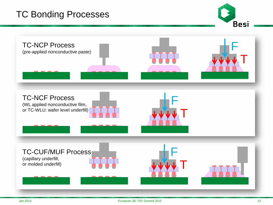
TC-NCP Process (pre-applied nonconductive paste)
TC-CUF/MUF Process (capillary underfill,
or molded underfill)
TC-NCF Process (WL applied nonconductive film,
or TC-WLU: wafer level underfill)
Jan-2015
TC Bonding Processes
14 European 3D TSV Summit 2015
T F
T F
T F

Jan-2015
TSV Stacking – High Volume Production
15 European 3D TSV Summit 2015
(Source: 2014 Hongkong Analyst Conference) Current Driver: HMC

Oct-2014
• Thermo compression bonder
• +200/-100 °C temperature
ramping
• 2µ @ 3 sigma accuracy
• 250 N bond force
• C2S / C2W
• TC/NCP, TC/NCF, TC/CUF
Datacon 8800 TC Thermo Compression Bonder
16 Confidential
8800 TC
Launch: March 2014
Now 12 x 8800 TC installed base
Preparing for 5 bonder / month shipment

Wafer and Panel transfer molding
Successor of compression molding
LARGE AREA MOLDING UP 340MMX340MM
eWLB and C2 WAFER APPLICATIONS
OVERMOLDED AND EXPOSED CAPABILITIES
GLASS AND SILICON INTERPOSER MOLDING
THIN MOLDCAP MOVING TO <0.150 MM

Key Advantages
Mold underfill (MUF) , proven on 30 um standoff: CUF, NCP, NCF obsolete
Use of Low cost compound : upto factor 3 x less
With use of topfoil : Exposed die without backgrind process
Compression molding Transfer molding
Backgrinding process is required
To expose the Die
Minimum mold
Gap over die
NCP or NCF required
Compound is coming from one side and
Can underfill and expose the die
Compound flow
Co
mp
ou
nd
flo
w

Equipment FML New wafer/panel molding system
Fico 19
Capability
• Wafer max Ǿ340 mm
• Panels max 300 x 300 mm
• Max. clampforce 1200 kN
• Max. compound pressure 180 bar
• Max. cavity temp diff. 3ºC
• Cavity vacuum control
• Board vacuum
• Dynamic clamping control
• Topfoil handling for exposed die
• Output max. 20 wafer/hour
Technical data
• Power rating 7.5 kVA
• Compressed air 5 – 10 bar
• Average air consumption 1.5 m³ at 6 bar
• Factory exhaust 100 m³/h
• Noise level 73 db(A)
• Dimensions (W x D x H) 720 x 1800 x 1700 mm
• Weight approx. 2000 kg
SEMI certified for S2; S8; S10; S14; S22

Thank You! April 2015