Embed Size (px)
Citation preview

This is information on a product in full production.
December 2017 DocID13698 Rev 6 1/47
TDA7719
Automotive 3 band car audio processor
Datasheet - production data
Features AEC-Q100 qualified Input multiplexer
– Multiple input configuration for differentapplication
Loudness– 2nd order frequency response– Programmable center frequency– 15 dB with 1 dB steps– Selectable high frequency boost– Selectable flat-mode
Volume– +15 dB to -15 dB with 1 dB step resolution– Soft-step control with programmable blend
times Bass
– 2nd order frequency response– Center frequency programmable in 4 steps– Q programmable 1.0/1.25/1.5/2.0– DC gain programmable– -15 to 15 dB range with 1 dB resolution
Middle– 2nd order frequency response– Center frequency programmable in 4 steps– Q programmable 0.5/0.75/1.0/1.25– -15 to 15 dB range with 1 dB resolution
Treble– 2nd order frequency response– Center frequency programmable in 4 steps– -15 to 15 dB range with 1 dB resolution
Speaker– 4 independent soft step speaker controls– 0 dB to -79 dB with 1 dB steps– Direct mute
Subwoofer– 2nd order low pass filter with programmable
cut off frequency– 2 independent soft step level control
Mute functions– Direct mute– Digitally controlled SoftMute with 4
programmable mute-times Offset detection
– Offset voltage detection circuit for on-boardpower amplifier failure diagnosis
Level meter– Provide rectified level voltage of main
source signal (before loudness) Rear seat selector
– Full source selector for rear seat output Mixing selector
DescriptionThe TDA7719 is a high performance signal processor specifically designed for car radio applications. The device includes a high performance audioprocessor with fully integrated audio filters and new Soft Step architecture. The digital control allows programming in a wide range of filter characteristics. By the use of BCMOS-process and liner signal processing low distortion and low noise are obtained
TSSOP28
Table 1. Device summaryOrder code Package Packing
TDA7719 TSSOP28 Tube
TDA7719TR TSSOP28 Tape and reel
www.st.com
Contents TDA7719
2/47 DocID13698 Rev 6
Contents
1 Block circuit diagram . . . . . . . . . . . . . . . . . . . . . . . . . . . . . . . . . . . . . . . . 6
2 Pin description . . . . . . . . . . . . . . . . . . . . . . . . . . . . . . . . . . . . . . . . . . . . . 72.1 Pin connection . . . . . . . . . . . . . . . . . . . . . . . . . . . . . . . . . . . . . . . . . . . . . . 7
2.2 Pin description . . . . . . . . . . . . . . . . . . . . . . . . . . . . . . . . . . . . . . . . . . . . . . 7
3 Electrical specifications . . . . . . . . . . . . . . . . . . . . . . . . . . . . . . . . . . . . . . 93.1 Thermal data . . . . . . . . . . . . . . . . . . . . . . . . . . . . . . . . . . . . . . . . . . . . . . . 9
3.2 Absolute maximum ratings . . . . . . . . . . . . . . . . . . . . . . . . . . . . . . . . . . . . . 9
3.3 Electrical characteristics . . . . . . . . . . . . . . . . . . . . . . . . . . . . . . . . . . . . . . . 9
4 Description . . . . . . . . . . . . . . . . . . . . . . . . . . . . . . . . . . . . . . . . . . . . . . . . 134.1 Input configuration . . . . . . . . . . . . . . . . . . . . . . . . . . . . . . . . . . . . . . . . . . 13
4.1.1 Front and rear selector . . . . . . . . . . . . . . . . . . . . . . . . . . . . . . . . . . . . . 13
4.1.2 Direct path . . . . . . . . . . . . . . . . . . . . . . . . . . . . . . . . . . . . . . . . . . . . . . . 15
4.2 Mixing . . . . . . . . . . . . . . . . . . . . . . . . . . . . . . . . . . . . . . . . . . . . . . . . . . . . 16
4.3 Loudness . . . . . . . . . . . . . . . . . . . . . . . . . . . . . . . . . . . . . . . . . . . . . . . . . 174.3.1 Loudness attenuation . . . . . . . . . . . . . . . . . . . . . . . . . . . . . . . . . . . . . . 17
4.3.2 Peak frequency . . . . . . . . . . . . . . . . . . . . . . . . . . . . . . . . . . . . . . . . . . . 17
4.3.3 High frequency boost . . . . . . . . . . . . . . . . . . . . . . . . . . . . . . . . . . . . . . . 18
4.3.4 Flat mode . . . . . . . . . . . . . . . . . . . . . . . . . . . . . . . . . . . . . . . . . . . . . . . . 18
4.4 SoftMute . . . . . . . . . . . . . . . . . . . . . . . . . . . . . . . . . . . . . . . . . . . . . . . . . . 18
4.5 Softstep volume . . . . . . . . . . . . . . . . . . . . . . . . . . . . . . . . . . . . . . . . . . . . 19
4.6 Bass . . . . . . . . . . . . . . . . . . . . . . . . . . . . . . . . . . . . . . . . . . . . . . . . . . . . . 194.6.1 Bass attenuation . . . . . . . . . . . . . . . . . . . . . . . . . . . . . . . . . . . . . . . . . . 19
4.6.2 Bass center frequency . . . . . . . . . . . . . . . . . . . . . . . . . . . . . . . . . . . . . . 19
4.6.3 Bass quality factors . . . . . . . . . . . . . . . . . . . . . . . . . . . . . . . . . . . . . . . . 20
4.6.4 DC mode . . . . . . . . . . . . . . . . . . . . . . . . . . . . . . . . . . . . . . . . . . . . . . . . 20
4.7 Middle . . . . . . . . . . . . . . . . . . . . . . . . . . . . . . . . . . . . . . . . . . . . . . . . . . . . 214.7.1 Middle attenuation . . . . . . . . . . . . . . . . . . . . . . . . . . . . . . . . . . . . . . . . . 21
4.7.2 Middle center frequency . . . . . . . . . . . . . . . . . . . . . . . . . . . . . . . . . . . . 21
4.7.3 Middle quality factors . . . . . . . . . . . . . . . . . . . . . . . . . . . . . . . . . . . . . . . 22
4.8 Treble . . . . . . . . . . . . . . . . . . . . . . . . . . . . . . . . . . . . . . . . . . . . . . . . . . . . 22

DocID13698 Rev 6 3/47
TDA7719 Contents
3
4.8.1 Treble attenuation . . . . . . . . . . . . . . . . . . . . . . . . . . . . . . . . . . . . . . . . . 22
4.8.2 Treble center frequency . . . . . . . . . . . . . . . . . . . . . . . . . . . . . . . . . . . . . 23
4.9 Subwoofer Filter . . . . . . . . . . . . . . . . . . . . . . . . . . . . . . . . . . . . . . . . . . . . 23
4.10 Softstep control . . . . . . . . . . . . . . . . . . . . . . . . . . . . . . . . . . . . . . . . . . . . 24
4.11 DC offset detector and level meter option . . . . . . . . . . . . . . . . . . . . . . . . 25
4.12 DC offset detector . . . . . . . . . . . . . . . . . . . . . . . . . . . . . . . . . . . . . . . . . . 25
4.13 Level meter . . . . . . . . . . . . . . . . . . . . . . . . . . . . . . . . . . . . . . . . . . . . . . . . 26
4.14 Output gain control . . . . . . . . . . . . . . . . . . . . . . . . . . . . . . . . . . . . . . . . . . 26
4.15 Audioprocessor testing . . . . . . . . . . . . . . . . . . . . . . . . . . . . . . . . . . . . . . . 26
4.16 Test circuit (3 x QD + 1 x FD + DC offset detector) . . . . . . . . . . . . . . . . . 27
5 I2C bus specification . . . . . . . . . . . . . . . . . . . . . . . . . . . . . . . . . . . . . . . . 285.1 Interface protocol . . . . . . . . . . . . . . . . . . . . . . . . . . . . . . . . . . . . . . . . . . . 28
5.1.1 Receive mode . . . . . . . . . . . . . . . . . . . . . . . . . . . . . . . . . . . . . . . . . . . . 29
5.1.2 Transmission mode . . . . . . . . . . . . . . . . . . . . . . . . . . . . . . . . . . . . . . . . 29
5.1.3 Reset condition . . . . . . . . . . . . . . . . . . . . . . . . . . . . . . . . . . . . . . . . . . . 29
5.2 Data byte specification . . . . . . . . . . . . . . . . . . . . . . . . . . . . . . . . . . . . . . . 31
6 Package information . . . . . . . . . . . . . . . . . . . . . . . . . . . . . . . . . . . . . . . . 446.1 TSSOP28 package information . . . . . . . . . . . . . . . . . . . . . . . . . . . . . . . . 44
7 Revision history . . . . . . . . . . . . . . . . . . . . . . . . . . . . . . . . . . . . . . . . . . . 46
List of tables TDA7719
4/47 DocID13698 Rev 6
List of tables
Table 1. Device summary . . . . . . . . . . . . . . . . . . . . . . . . . . . . . . . . . . . . . . . . . . . . . . . . . . . . . . . . . . 1Table 2. Pin description . . . . . . . . . . . . . . . . . . . . . . . . . . . . . . . . . . . . . . . . . . . . . . . . . . . . . . . . . . . 7Table 3. Thermal data. . . . . . . . . . . . . . . . . . . . . . . . . . . . . . . . . . . . . . . . . . . . . . . . . . . . . . . . . . . . . 9Table 4. Absolute maximum ratings . . . . . . . . . . . . . . . . . . . . . . . . . . . . . . . . . . . . . . . . . . . . . . . . . . 9Table 5. Electrical characteristics . . . . . . . . . . . . . . . . . . . . . . . . . . . . . . . . . . . . . . . . . . . . . . . . . . . . 9Table 6. Input pin configuration . . . . . . . . . . . . . . . . . . . . . . . . . . . . . . . . . . . . . . . . . . . . . . . . . . . . 13Table 7. Selector configuration matrix . . . . . . . . . . . . . . . . . . . . . . . . . . . . . . . . . . . . . . . . . . . . . . . 14Table 8. Available sources for mixing . . . . . . . . . . . . . . . . . . . . . . . . . . . . . . . . . . . . . . . . . . . . . . . . 16Table 9. I2C bus electrical characteristics. . . . . . . . . . . . . . . . . . . . . . . . . . . . . . . . . . . . . . . . . . . . . 28Table 10. Subaddress (receive mode) . . . . . . . . . . . . . . . . . . . . . . . . . . . . . . . . . . . . . . . . . . . . . . . . 30Table 11. Input configuration / main selector (0). . . . . . . . . . . . . . . . . . . . . . . . . . . . . . . . . . . . . . . . . 31Table 12. 2nd Source selector / direct path (1). . . . . . . . . . . . . . . . . . . . . . . . . . . . . . . . . . . . . . . . . . 32Table 13. Mixing source / mixing gain (2) . . . . . . . . . . . . . . . . . . . . . . . . . . . . . . . . . . . . . . . . . . . . . . 33Table 14. Mix control / level meter / dc offset detector configure (3) . . . . . . . . . . . . . . . . . . . . . . . . . 34Table 15. Soft mute / others (4) . . . . . . . . . . . . . . . . . . . . . . . . . . . . . . . . . . . . . . . . . . . . . . . . . . . . . 35Table 16. SoftStep I (5). . . . . . . . . . . . . . . . . . . . . . . . . . . . . . . . . . . . . . . . . . . . . . . . . . . . . . . . . . . . 36Table 17. SoftStep II / DC detector (6) . . . . . . . . . . . . . . . . . . . . . . . . . . . . . . . . . . . . . . . . . . . . . . . . 37Table 18. Loudness (7) . . . . . . . . . . . . . . . . . . . . . . . . . . . . . . . . . . . . . . . . . . . . . . . . . . . . . . . . . . . . 38Table 19. Volume / output gain (8) . . . . . . . . . . . . . . . . . . . . . . . . . . . . . . . . . . . . . . . . . . . . . . . . . . . 38Table 20. Treble filter (9). . . . . . . . . . . . . . . . . . . . . . . . . . . . . . . . . . . . . . . . . . . . . . . . . . . . . . . . . . . 39Table 21. Middle filter (10) . . . . . . . . . . . . . . . . . . . . . . . . . . . . . . . . . . . . . . . . . . . . . . . . . . . . . . . . . 39Table 22. Bass filter (11). . . . . . . . . . . . . . . . . . . . . . . . . . . . . . . . . . . . . . . . . . . . . . . . . . . . . . . . . . . 40Table 23. Subwoofer / middle / bass (12) . . . . . . . . . . . . . . . . . . . . . . . . . . . . . . . . . . . . . . . . . . . . . . 40Table 24. Speaker attenuation (LF/RF/LR/RR) (13-16) . . . . . . . . . . . . . . . . . . . . . . . . . . . . . . . . . . . 41Table 25. Subwoofer attenuation (subwoofer L/subwoofer R) (17-18) . . . . . . . . . . . . . . . . . . . . . . . . 41Table 26. Testing audio processor 1 (19) . . . . . . . . . . . . . . . . . . . . . . . . . . . . . . . . . . . . . . . . . . . . . . 42Table 27. Testing audio processor 2 (20) . . . . . . . . . . . . . . . . . . . . . . . . . . . . . . . . . . . . . . . . . . . . . . 43Table 28. TSSOP28 package mechanical data . . . . . . . . . . . . . . . . . . . . . . . . . . . . . . . . . . . . . . . . . 45Table 29. Document revision history. . . . . . . . . . . . . . . . . . . . . . . . . . . . . . . . . . . . . . . . . . . . . . . . . . 46
DocID13698 Rev 6 5/47
TDA7719 List of figures
5
List of figures
Figure 1. Block circuit diagram. . . . . . . . . . . . . . . . . . . . . . . . . . . . . . . . . . . . . . . . . . . . . . . . . . . . . . . 6Figure 2. Pin connection (top view) . . . . . . . . . . . . . . . . . . . . . . . . . . . . . . . . . . . . . . . . . . . . . . . . . . . 7Figure 3. QD and FD configuration of QD4/FD4 . . . . . . . . . . . . . . . . . . . . . . . . . . . . . . . . . . . . . . . . 15Figure 4. Block diagram of mixing stage . . . . . . . . . . . . . . . . . . . . . . . . . . . . . . . . . . . . . . . . . . . . . . 16Figure 5. Loudness attenuation @ fP = 400 Hz. . . . . . . . . . . . . . . . . . . . . . . . . . . . . . . . . . . . . . . . . 17Figure 6. Loudness center frequencies @ Attn. = 15 dB. . . . . . . . . . . . . . . . . . . . . . . . . . . . . . . . . . 17Figure 7. Loudness attenuation, fc =2.4 kHz . . . . . . . . . . . . . . . . . . . . . . . . . . . . . . . . . . . . . . . . . . . 18Figure 8. SoftMute timing. . . . . . . . . . . . . . . . . . . . . . . . . . . . . . . . . . . . . . . . . . . . . . . . . . . . . . . . . . 18Figure 9. Bass Control @ fc = 80 Hz, Q = 1 . . . . . . . . . . . . . . . . . . . . . . . . . . . . . . . . . . . . . . . . . . . 19Figure 10. Bass center frequencies @ gain = 14 dB, Q = 1 . . . . . . . . . . . . . . . . . . . . . . . . . . . . . . . . 19Figure 11. Bass quality factors @ gain = 14 dB, fc = 80 Hz. . . . . . . . . . . . . . . . . . . . . . . . . . . . . . . . . 20Figure 12. Bass normal and DC mode @ Gain = 14 dB, fc = 80 Hz . . . . . . . . . . . . . . . . . . . . . . . . . . 20Figure 13. Middle control @ fc = 1 kHz, Q = 1. . . . . . . . . . . . . . . . . . . . . . . . . . . . . . . . . . . . . . . . . . . 21Figure 14. Middle center frequencies @ gain = 14d B, Q = 1 . . . . . . . . . . . . . . . . . . . . . . . . . . . . . . . 21Figure 15. Middle quality factors @ gain = 14 dB, fc = 1 kHz . . . . . . . . . . . . . . . . . . . . . . . . . . . . . . . 22Figure 16. Treble Control @ fc = 17.5 kHz. . . . . . . . . . . . . . . . . . . . . . . . . . . . . . . . . . . . . . . . . . . . . . 22Figure 17. Treble center frequencies @ gain = 14 dB . . . . . . . . . . . . . . . . . . . . . . . . . . . . . . . . . . . . . 23Figure 18. Subwoofer control . . . . . . . . . . . . . . . . . . . . . . . . . . . . . . . . . . . . . . . . . . . . . . . . . . . . . . . . 23Figure 19. DC offset detection circuit (simplified). . . . . . . . . . . . . . . . . . . . . . . . . . . . . . . . . . . . . . . . . 26Figure 20. Test circuit. . . . . . . . . . . . . . . . . . . . . . . . . . . . . . . . . . . . . . . . . . . . . . . . . . . . . . . . . . . . . . 27Figure 21. Switching characteristics. . . . . . . . . . . . . . . . . . . . . . . . . . . . . . . . . . . . . . . . . . . . . . . . . . . 28Figure 22. I2C timing diagram . . . . . . . . . . . . . . . . . . . . . . . . . . . . . . . . . . . . . . . . . . . . . . . . . . . . . . . 29Figure 23. TSSOP28 package outline . . . . . . . . . . . . . . . . . . . . . . . . . . . . . . . . . . . . . . . . . . . . . . . . . 44
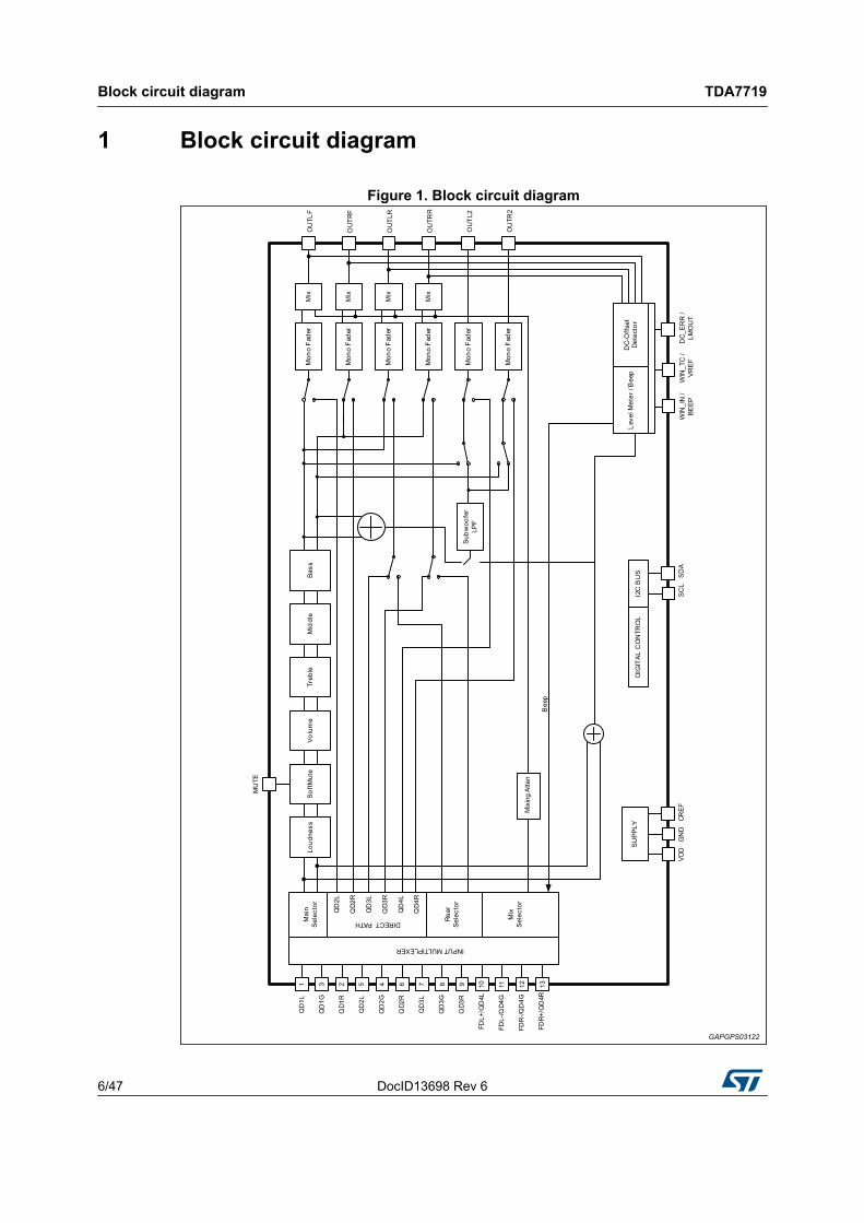
Block circuit diagram TDA7719
6/47 DocID13698 Rev 6
1 Block circuit diagram
Figure 1. Block circuit diagram

DocID13698 Rev 6 7/47
TDA7719 Pin description
46
2 Pin description
2.1 Pin connection
Figure 2. Pin connection (top view)
2.2 Pin description
Table 2. Pin description No. Pin name Description I/O
1 QD1L / SE1L / MD3+ QD1 left input or SE1 left or MD3 positive input I/O
2 QD1R / SE1R / MD3- QD1 right input or SE1 right input or MD3 negative input I/O
3 QD1G / SE2L QD1 common input or SE2 left input I/O
4 QD2G / SE2R QD2 common input or SE2 right input I/O
5 QD2L / SE3L QD2 left input or SE3 left input I/O
6 QD2R / SE3R QD2 right input or SE3 right input I/O
7 QD3L QD3 left input I/O
8 QD3G QD3 common input I/O
9 QD3R QD3 right input I/O
10 QD4L / FD4L+ / SE4L / MD1+ QD4 left input or FD4L positive input or SE4 left input or MD1 positive input I/O
11 QD4G / FD4L- / SE4R / MD1- QD4 common input or FD4L negative input or SE4 right input or MD1 negative input I/O

Pin description TDA7719
8/47 DocID13698 Rev 6
12 QD4G / FD4R- / SE5L / MD2- QD4 common input or FD4R negative input or SE5 left input or MD2 negative input I/O
13 QD4R / FD4R+ / SE5R / MD2+ QD4 right input or FD4R positive input or SE5 right input or MD2 positive input I/O
14 CREF Reference capacitor O
15 GND Ground S
16 OUTR2 Subwoofer output / 2nd right output O
17 OUTL2 Subwoofer output / 2nd left output O
18 OUTRF Front right output O
19 OUTRR Rear right output O
20 OUTLR Rear left output O
21 OUTLF Front left output O
22 WinTC / VREF DC offset detector filter or Vref output O
23 MUTE I2C bus data I/O
24 VDD Supply S
25 SCL I2C bus clock I
26 SDA I2C bus data I/O
27 DC_ERR / LMOUT DC offset detector output or Level meter output O
28 WIN_IN / Beep DC offset detector input or Beep input (Mono Single-Ended input) I
Table 2. Pin description (continued)No. Pin name Description I/O
DocID13698 Rev 6 9/47
TDA7719 Electrical specifications
46
3 Electrical specifications
3.1 Thermal data
3.2 Absolute maximum ratings
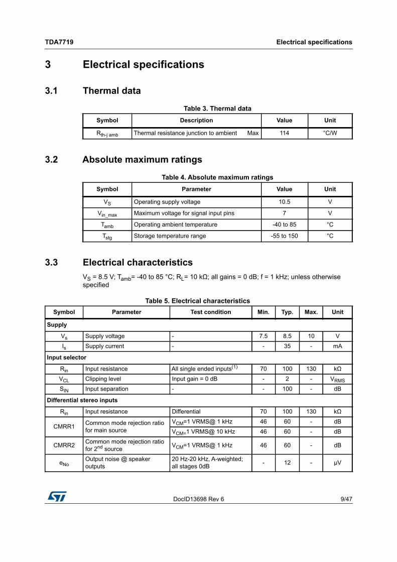
3.3 Electrical characteristicsVS = 8.5 V; Tamb= -40 to 85 °C; RL= 10 kΩ; all gains = 0 dB; f = 1 kHz; unless otherwise specified
Table 3. Thermal dataSymbol Description Value Unit
Rth-j amb Thermal resistance junction to ambient Max 114 °C/W
Table 4. Absolute maximum ratingsSymbol Parameter Value Unit
VS Operating supply voltage 10.5 V
Vin_max Maximum voltage for signal input pins 7 V
Tamb Operating ambient temperature -40 to 85 °C
Tstg Storage temperature range -55 to 150 °C
Table 5. Electrical characteristics Symbol Parameter Test condition Min. Typ. Max. Unit
Supply
Vs Supply voltage - 7.5 8.5 10 V
Is Supply current - - 35 - mA
Input selector
Rin Input resistance All single ended inputs(1) 70 100 130 kΩ
VCL Clipping level Input gain = 0 dB - 2 - VRMS
SIN Input separation - - 100 - dB
Differential stereo inputs
Rin Input resistance Differential 70 100 130 kΩ
CMRR1 Common mode rejection ratio for main source
VCM=1 VRMS@ 1 kHz 46 60 - dB
VCM=1 VRMS@ 10 kHz 46 60 - dB
CMRR2 Common mode rejection ratio for 2nd source VCM=1 VRMS@ 1 kHz 46 60 - dB
eNoOutput noise @ speaker outputs
20 Hz-20 kHz, A-weighted; all stages 0dB - 12 - μV

Electrical specifications TDA7719
10/47 DocID13698 Rev 6
Loudness control
AMAX Max attenuation - - 15 - dB
ASTEP Step resolution - - 1 - dB
fPeak Peak frequency
fP1 - 400 - Hz
fP2 - 800 - Hz
fP3 - 2400 - Hz
Volume control
GMAX Max gain - - 15 - dB
AMAX Max attenuation - - -15 - dB
ASTEP Step resolution - 0.5 1 1.5 dB
EA Attenuation set error - -0.75 0 +0.75 dB
ET Tracking error - - - 2 dB
VDC DC stepsAdjacent attenuation steps - 0.1 3 mV
From 0 dB to GMIN - 0.5 5 mV
Soft mute
AMUTE Mute attenuation - 80 100 - dB
TD Delay time
T1 - 0.48 - ms
T2 - 0.96 - ms
T3 - 8 ms
T4 - 16 - ms
VTH Low Low threshold for SM pin - - - 1 V
VTH High High threshold for SM pin - 2.5 - - V
RPU Internal pull-up resistor - 32 45 58 kΩ
VPU Internal pull-up Voltage - - 3.3 - V
Bass control
Fc Center frequency
fC1 54 60 66 Hz
fC2 72 80 88 Hz
fC3 90 100 110 Hz
fC4 180 200 220 Hz
QBASS Quality factor
Q1 0.9 1 1.1 -
Q2 1.1 1.25 1.4 -
Q3 1.3 1.5 1.7 -
Q4 1.8 2 2.2 -
CRANGE Control range - ±14 ±15 ±16 dB
ASTEP Step resolution - 0.5 1 1.5 dB
DCGAIN Bass-DC-gainDC = off -1 0 +1 dB
DC = on, Gain = 15 dB - ±4.4 dB
Table 5. Electrical characteristics (continued)Symbol Parameter Test condition Min. Typ. Max. Unit

DocID13698 Rev 6 11/47
TDA7719 Electrical specifications
46
Middle control
CRANGE Control range - ±14 ±15 ±16 dB
ASTEP Step resolution - 0.5 1 1.5 dB
fc Center frequency
fC1 400 500 600 Hz
fC2 0.8 1 1.2 kHz
fC3 1.2 1.5 1.8 kHz
fC4 2 2.5 3 kHz
QBASS Quality factor
Q1 0.45 0.5 0.55 -
Q2 0.65 0.75 0.85 -
Q3 0.9 1 1.1 -
Q4 1.1 1.25 1.4 -
Treble control
CRANGE Clipping level ±14 ±15 ±16 dB
ASTEP Step resolution 0.5 1 1.5 dB
fc Center frequency
fC1 8 10 12 kHz
fC2 10 12.5 15 kHz
fC3 12 15 18 kHz
fC4 14 17.5 21 kHz
Speaker attenuators
AMIN Min attenuation - -1 0 1 dB
AMAX Max attenuation - -89 -79 -69 dB
ASTEP Step resolution - 0.5 1 1.5 dB
AMUTE Mute attenuation - 80 90 dB
EE Attenuation set error - - - 2 dB
VDC DC steps Adjacent attenuation steps - 0.1 5 mV
Audio outputs
VCL Clipping leveld = 0.3%; Byte8_D6=1 2 - - VRMS
d = 1%; Byte8_D6=0 2.2 - - VRMS
ROUT Output impedance - - 30 100 Ω
RL Output load resistance - 2 - - kΩ
CL Output load capacitor - - - 10 nF
VDC DC voltage level - 3.8 4.0 4.2 V
Subwoofer attenuator
GMAX Max gain - 14 15 16 dB
AMAX Max attenuation - -83 -79 -75 dB
ASTEP Step resolution - 0.5 1 1.5 dB
AMUTE Mute attenuation - 80 90 - dB
EE Attenuation set error - - - 2 dB
Table 5. Electrical characteristics (continued)Symbol Parameter Test condition Min. Typ. Max. Unit

Electrical specifications TDA7719
12/47 DocID13698 Rev 6
VDC DC steps Adjacent attenuation steps - 0.1 5 mV
Subwoofer lowpass
fLP Lowpass corner frequency
fLP1 72 80 88 Hz
fLP2 108 120 132 Hz
fLP3 144 160 176 Hz
DC offset detection circuit
Vth Zero comp window size
V1 - ±25 - mV
V2 - ±50 - mV
V3 - ±75 - mV
V4 - ±100 - mV
tsp Max rejected spike length
- - 11 - μs
- - 22 - μs
- - 33 - μs
- - 44 - μs
ICHDCErr DCErr charge current - - 5 - μA
IDISDCErr DCErr discharge current - - 5 - mA
VOutH DCErr high volotage - - 3.3 - V
VOutH DCErr low voltage - - 100 - mV
Level meter
Vout Output voltage range - 0 3.3 V
VLEVEL Output levelVin = 1 Vrms - 1.6 - V
Vin = AC grounded - 0 - V
TDEL Analog output delay time - - 2 - μs
General
eNO Output noise
BW = 20 Hz to 20 kHz A-Weighted, all gain = 0 dB - 12 - μV
BW = 20 Hz - 20 kHz A-Weighted, output muted - 6 - μV
S/N Signal to noise ratio all gain = 0 dB, A-weighted; Vo = 2 VRMS
- 104 - dB
D Distortion VIN =1 VRMS; all stages 0dB - 0.01 - %
SC Channel separation left/right - - 90 - dB
1. When DC offset detector is not used, the impedance of mono single-ended input is 50 k instead of 100 k.
Table 5. Electrical characteristics (continued)Symbol Parameter Test condition Min. Typ. Max. Unit

DocID13698 Rev 6 13/47
TDA7719 Description
46
4 Description
4.1 Input configuration
4.1.1 Front and rear selectorThe input stage (Main source and 2nd source) is configurable to adapt to different application. There are 7 different configurations which provide different input structure and different number of input sources as shown below. 4 x QD, 2 x QD + 3 x SE, 1 x QD + 5 x SE, 1 x QD + 3 x SE + 2 x MD, 3 x QD + 1 x FD, 3 x QD + 2 x SE, 1 x QD + 2 x SE + 1 x FD + 1 x MD, 1 x QD + 3 x SE + 1 x FD
Note: QD = Quasi-Differential, SE = Single-ended input, FD = Full Differential, MD = mono Differential
The configuration of the input stage is controlled by ‘Input Configuration’ bits in I2C control table (Byte0 Bit5~Bit7). The table below shows the configuration of input pins in different configurations.
Table 6. Input pin configuration
Pin Pin name
Configuration bits (Byte0 Bit7~Bit5)
"000" "001" "010" "011" "100" "101" "110" "111"
CFG0 CFG1 CFG2 CFG3 CFG4 CFG5 CFG6 CFG7
1 QD1L_SE1L _MD3+ QD1L
IN0
SE1LIN0
SE1LIN0
SE1LIN0
QD1L
IN0
QD1L
IN0
MD3+IN7
SE1LIN0
2 QD1R_SE1R _MD3- QD1R SE1R SE1R SE1R QD1R QD1R MD3- SE1R
3 QD1G_SE2L QD1G SE2LIN4
SE2LIN4
SE2LIN4
QD1G QD1G SE2LIN4
SE2LIN4
4 QD2G_SE2R QD2G
IN1
SE2R SE2R SE2R QD2G
IN1
QD2G
IN1
SE2R SE2R
5 QD2L_SE3L QD2L SE3LIN1
SE3LIN1
SE3LIN1
QD2L QD2L SE3LIN1
SE3LIN1
6 QD2R_SE3R QD2R SE3R SE3R SE3R QD2R QD2R SE3R SE3R
7 QD3L QD3L
IN2
QD3L
IN2
QD3L
IN2
QD3L
IN2
QD3L
IN2
QD3L
IN2
QD3L
IN2
QD3L
IN28 QD3G QD3G QD3G QD3G QD3G QD3G QD3G QD3G QD3G
9 QD3R QD3R QD3R QD3R QD3R QD3R QD3R QD3R QD3R
10 QD4L_FD4+ _SE4L_MD1+ QD4L
IN3
QD4L
IN3
SE4LIN5
MD1+IN3
FD4L+
IN3
SE4LIN5
FD4L+
IN3
FD4L+
IN311 QD4G_FD4L
_SE4R_MD1- QD4G QD4G SE4R MD1- FD4L- SE4R FD4L- FD4L-
12 QD4G_FD4R_SE5L_MD2- QD4G QD4G SE5L
IN6MD2-
IN3FD4R- SE5L
IN6FD4R- FD4R-
13 QD4R_FD4R+_SE5R_MD2+ QD4R QD4R SE5R MD2+ FD4R
+ SE5R FD4R+ FD4R+
Description TDA7719
14/47 DocID13698 Rev 6
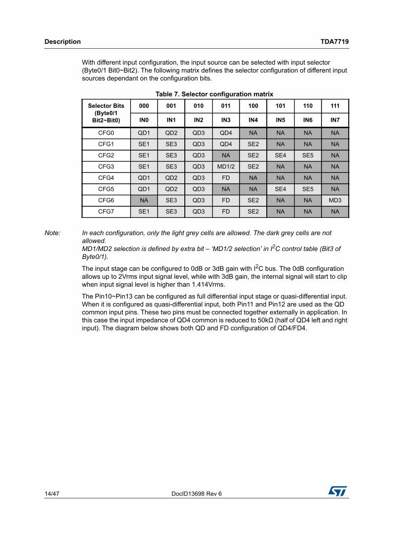
With different input configuration, the input source can be selected with input selector (Byte0/1 Bit0~Bit2). The following matrix defines the selector configuration of different input sources dependant on the configuration bits.
Note: In each configuration, only the light grey cells are allowed. The dark grey cells are not allowed. MD1/MD2 selection is defined by extra bit – ‘MD1/2 selection’ in I2C control table (Bit3 of Byte0/1).
The input stage can be configured to 0dB or 3dB gain with I2C bus. The 0dB configuration allows up to 2Vrms input signal level, while with 3dB gain, the internal signal will start to clip when input signal level is higher than 1.414Vrms.
The Pin10~Pin13 can be configured as full differential input stage or quasi-differential input. When it is configured as quasi-differential input, both Pin11 and Pin12 are used as the QD common input pins. These two pins must be connected together externally in application. In this case the input impedance of QD4 common is reduced to 50kΩ (half of QD4 left and right input). The diagram below shows both QD and FD configuration of QD4/FD4.
Table 7. Selector configuration matrix Selector Bits
(Byte0/1 Bit2~Bit0)
000 001 010 011 100 101 110 111
IN0 IN1 IN2 IN3 IN4 IN5 IN6 IN7
CFG0 QD1 QD2 QD3 QD4 NA NA NA NA
CFG1 SE1 SE3 QD3 QD4 SE2 NA NA NA
CFG2 SE1 SE3 QD3 NA SE2 SE4 SE5 NA
CFG3 SE1 SE3 QD3 MD1/2 SE2 NA NA NA
CFG4 QD1 QD2 QD3 FD NA NA NA NA
CFG5 QD1 QD2 QD3 NA NA SE4 SE5 NA
CFG6 NA SE3 QD3 FD SE2 NA NA MD3
CFG7 SE1 SE3 QD3 FD SE2 NA NA NA

DocID13698 Rev 6 15/47
TDA7719 Description
46
Figure 3. QD and FD configuration of QD4/FD4
4.1.2 Direct pathThe input pins can be configured as direct path mode by setting Byte1 Bit5~Bit7. In direct path mode the input pins are connected to dedicated mono fader directly, all the filters and volume are bypassed. Below is described the assignment of the input pins and output fader in direct path mode:
Pin5/QD2L --> OUTLF
Pin6/QD2R --> OUTRF
Pin7/QD3L --> OUTLR
Pin9/QD3R --> OUTRR
Pin10/FDL+_QD4L --> OUTL2
Pin13/FDR+_QD4R--> OUTR2
Note: The configurations CFG2, CFG3 and CFG5 are not recommended in direct path mode. Because in these 3 configurations SE4L/MD1+ and SE5R/MD2+ are connected to OUT2_L and OUT2_R fader separately. In this case left and right channel of OUT2 belongs to different input sources.If the direct path is chosen, the input pins have to be used as single ended pins. In case of differential inputs the ground or minus pins must be connect to GND by AC short.Inputs in direct path mode are also selectable with front and rear selector.

Description TDA7719
16/47 DocID13698 Rev 6
4.2 MixingThe device provides mixing function which allows the mixing source mixed into front and rear speaker output independently. The mixing source can be any single-ended input, mono-differential input or beep input (Mono single-ended input when DC offset detector is not used). In order to adjust the level of mixing signal, the mixing selector is followed with a 0 dB~-31 dB attenuator. The maximum mixing input signal level is 1.6 Vrms for single-ended input and mono-differential input. For beep input, the maximum input signal level is about 1.4 Vrms. The block diagram of the mixing function is shown below.
Figure 4. Block diagram of mixing stage
Since the input stage of this device has different configurations, the corresponding sources for mixing selector are also different according to the configurations. The following table defines the available sources for mixing under different configurations.
Note: Only light grey cells are allowed mixing input. The dark grey cells are not allowed. The beep input is available only when DC offset detector function is not used.
Table 8. Available sources for mixing
Mix selector bits (Byte2 Bit2~Bit0)
000 001 010 011 100 101 110 111
MixIN0 MixIN1 MixIN2 MixIN3 MixIN4 MixIN5 MixIN6 MixIN7
CFG0 NA NA NA NA NA NA Beep Mute
CFG1 SE1 SE2 SE3 NA NA NA Beep Mute
CFG2 SE1 SE2 SE3 SE4 SE5 NA Beep Mute
CFG3 SE1 SE2 SE3 MD1 NA MD2 Beep Mute
CFG4 NA NA NA NA NA NA Beep Mute
CFG5 NA NA NA SE4 SE5 NA Beep Mute
CFG6 MD3 SE2 SE3 NA NA NA Beep Mute
CFG7 SE1 SE2 SE3 NA NA NA Beep Mute

DocID13698 Rev 6 17/47
TDA7719 Description
46
4.3 LoudnessThere are four parameters programmable in the loudness stage:
4.3.1 Loudness attenuationFigure 5 shows the attenuation as a function of frequency at fP = 400 Hz
Figure 5. Loudness attenuation @ fP = 400 Hz.
4.3.2 Peak frequencyFigure 6 shows the four possible peak-frequencies at 400, 800 and 2400 Hz
Figure 6. Loudness center frequencies @ Attn. = 15 dB.
Description TDA7719
18/47 DocID13698 Rev 6
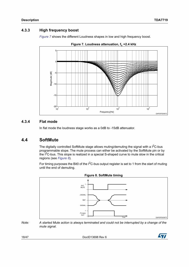
4.3.3 High frequency boostFigure 7 shows the different Loudness shapes in low and high frequency boost.
Figure 7. Loudness attenuation, fc =2.4 kHz
4.3.4 Flat modeIn flat mode the loudness stage works as a 0dB to -15dB attenuator.
4.4 SoftMuteThe digitally controlled SoftMute stage allows muting/demuting the signal with a I2C-bus programmable slope. The mute process can either be activated by the SoftMute pin or by the I2C-bus. This slope is realized in a special S-shaped curve to mute slow in the critical regions (see Figure 8).
For timing purposes the Bit0 of the I2C-bus output register is set to 1 from the start of muting until the end of demuting.
Figure 8. SoftMute timing
Note: A started Mute action is always terminated and could not be interrupted by a change of the mute signal.

DocID13698 Rev 6 19/47
TDA7719 Description
46
4.5 Softstep volumeWhen the volume-level is changed audible clicks could appear at the output. The root cause of those clicks could either be a DC Offset before the volume-stage or the sudden change of the envelope of the audio signal. With the Softstep feature both kinds of clicks could be reduced to a minimum and are no more audible. The blend-time from one step to the next is programmable as 5 ms or 10 ms. The softstep control is described in detail in Chapter 4.10.
4.6 BassThere are four parameters programmable in the bass stage:
4.6.1 Bass attenuationFigure 9 shows the attenuation as a function of frequency at a center frequency of 80 Hz.
Figure 9. Bass Control @ fc = 80 Hz, Q = 1
4.6.2 Bass center frequencyFigure 10 shows the four possible center frequencies 60, 80, 100 and 200 Hz.
Figure 10. Bass center frequencies @ gain = 14 dB, Q = 1

Description TDA7719
20/47 DocID13698 Rev 6
4.6.3 Bass quality factorsFigure 11 shows the four possible quality factors 1, 1.25, 1.5 and 2.
Figure 11. Bass quality factors @ gain = 14 dB, fc = 80 Hz
4.6.4 DC modeIn this mode the DC gain is increased by 4.4 dB. In addition the programmed center frequency and quality factor is decreased by 25 % which can be used to reach alternative center frequencies or quality factors.
Figure 12. Bass normal and DC mode @ Gain = 14 dB, fc = 80 Hz
Note: The center frequency, Q and DC-mode can be set fully independently.

DocID13698 Rev 6 21/47
TDA7719 Description
46
4.7 MiddleThere are three parameters programmable in the middle stage:
4.7.1 Middle attenuationFigure 13 shows the attenuation as a function of frequency at a center frequency of 1 kHz.
Figure 13. Middle control @ fc = 1 kHz, Q = 1
4.7.2 Middle center frequencyFigure 14 shows the four possible center frequencies 500 Hz, 1 kHz, 1.5 kHz and 2.5 kHz.
Figure 14. Middle center frequencies @ gain = 14d B, Q = 1

Description TDA7719
22/47 DocID13698 Rev 6
4.7.3 Middle quality factorsFigure 15 shows the four possible quality factors 0.5, 0.75, 1 and 1.25.
Figure 15. Middle quality factors @ gain = 14 dB, fc = 1 kHz
4.8 TrebleThere are two parameters programmable in the treble stage:
4.8.1 Treble attenuationFigure 16 shows the attenuation as a function of frequency at a center frequency of 17.5 kHz.
Figure 16. Treble Control @ fc = 17.5 kHz.

DocID13698 Rev 6 23/47
TDA7719 Description
46
4.8.2 Treble center frequencyFigure 17 shows the four possible center frequencies 10 k, 12.5 k, 15 k and 17.5 kHz.
Figure 17. Treble center frequencies @ gain = 14 dB
4.9 Subwoofer FilterThe subwoofer lowpass filter has Butterworth characteristics with programmable cut-off frequency (80 / 120 / 160 Hz). The output phase can be selected between 0 deg and 180 deg. The input of subwoofer takes signal from bass filter output or output of input mux.
Figure 18. Subwoofer control

Description TDA7719
24/47 DocID13698 Rev 6
4.10 Softstep controlIn this device, the softstep function is available for volume, speaker, loudness, treble, middle and bass block. With softstep function, the audible noise of DC offset or the sudden change of signal can be avoided when adjusting gain setting of the block.
For each block, the softstep function is controlled by softstep on/off control bit in the control table. The softstep transient time selection (5 ms or 10 ms) is common for all blocks and it is controlled by softstep time control bit. The softstep operation of all blocks has a common centralized control. In this case, a new softstep operation can not be started before the completion previous softstep.
There are two different modes to activate the softstep operation. The softstep operation can be started right after I2C data sending, or the softstep can be activated in parallel after data sending of several different blocks. The two modes are controlled by the ‘act bit’ (it is normally bit7 of the byte.) of each byte. When act bit is ‘0’, which means action, the softstep is activated right after the date byte is sent. When the act bit is ‘1’, which means wait, the block goes to wait for softstep status. In this case, the block will wait for some other block to activate the operation. The softstep operation of all blocks in wait status will be done together with the block which activate the softstep. With this mode, all specific blocks can do the softstep in parallel. This avoids waiting when the softstep is operated one by one.
Chip Addr Sub Addr 0xxxxxxx
| Softstep start here
Chip Addr Sub Addr 1xxxxxxx 1xxxxxxx ...... 0xxxxxxx
| Softstep start here for all
1. It is not allowed to cross 0 dB with softstep directly. From plus gain to minus gain, it must go to +0 dB first, then destination. From minus gain to plus gain, it must go to -0 dB first, and then destination.
2. When one block is in ‘wait for softstep’ status, it is not allowed to send data to this block again before its softstep is completed.
3. To know if there is a softstep in operation, it is possible to monitor the ‘busy’ signal by I2C transmission mode (Section 5.1.2). When softstep is busy (busy=0), it is better to wait before sending new data until it is free (busy=1).

DocID13698 Rev 6 25/47
TDA7719 Description
46
4.11 DC offset detector and level meter optionThis device provide DC offset detector function and level meter function option. In one specific application, only one of the function can be used. The configuration of the function is controlled by I2C bus (Byte3 Bit7).
When the device uses DC offset detector function, Pin22, Pin27 and Pin28 are used as WinTC, DCErr and WinIN for DC offset detector. When it is configured as level meter, DCErr becomes level meter output. In the mean time, WinIN is used as beep input (Mono single-ended input for mixing), and WinTC becomes a reference voltage output (4 V external DC voltage or 3.3 V internal reference voltage).
4.12 DC offset detectorUsing the DC offset detection circuit (Figure 19) an offset voltage difference between the audio power amplifier and the TDA7719's Front and Rear outputs can be detected, preventing serious damage to the loudspeakers. The circuit compares whether the signal crosses the zero level inside the audio power at the same time as in the speaker cell. The output of the zero-window-comparator of the power amplifier must be connected with the WinIn-input of the TDA7719. The WinIn-input has an internal pull-up resistor connected to 5.5 V. It is recommended to drive this pin with open-collector outputs only.
To compensate for errors at low frequencies the WinTC-pin are implemented, with external capacitors introducing the same delay = 7.5k * Cext as the AC-coupling between the TDA7719 and the power amplifier introduces. For the zero window comparators, the time constant for spike rejection as well as the threshold are programmable.
For electrical characteristics see Chapter 3 on page 9.
A low-active DC-offset error signal appears at the DCErr output if the next conditions are both true:
a) Front and rear outputs are inside zero crossing windows.b) The Input voltage VWinIn is logic low whenever at least one output of the power
amplifier is outside the zero crossing windows.
After power-on, the external attached capacitor is rapidly charged (fast-charge) to overcome a false indication.

Description TDA7719
26/47 DocID13698 Rev 6
Figure 19. DC offset detection circuit (simplified)
4.13 Level meterIn case of not using DC offset detector, the three pins used for DCO can be configured as other function. Pin27 (DC_Err / LMOUT) becomes the level meter output. The level meter block takes signal after main input selector and mix signal into mono, then rectify the signal and detect the peak of the signal. The output stage of level meter removes the DC voltage of the signal and the output voltage level shows exactly the Vpeak of signal. Since the discharge time constant of the level meter is quite slow, it is necessary to reset level meter regularly (with I2C bus control Byte3 Bit6) to get correct peak information of the signal.
4.14 Output gain controlThe output stage of the device can provide a option to have additional 1 dB gain in order to boost the maximum output level to 2.2 Vrms with maximum 1 % distortion.
4.15 Audioprocessor testingIn the test mode, which can be activated by setting bit D7 of the I2C subaddress byte and bit D0 of the testing-audioprocessor byte, several internal signals are available at the QD1L pin. In this mode, the input resistance of 100 kΩ is disconnected from the pin. Internal signals available for testing are listed in the data-byte specification.
DocID13698 Rev 6 27/47
TDA7719 Description
46
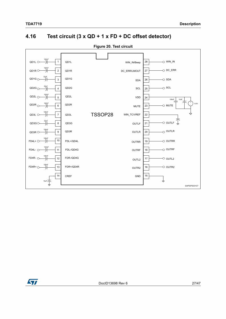
4.16 Test circuit (3 x QD + 1 x FD + DC offset detector)
Figure 20. Test circuit

I2C bus specification TDA7719
28/47 DocID13698 Rev 6
5 I2C bus specification
5.1 Interface protocolThe interface protocol comprises: a start condition (S) a chip address byte (the LSB determines read/write transmission) a subaddress byte a sequence of data (N-bytes + acknowledge) a stop condition (P) the max. clock speed is 400 kbits/s 3.3 V logic compatible
Figure 21. Switching characteristics
S = Start ACK = Acknowledge
Table 9. I2C bus electrical characteristics Symbol Parameter Min Max Unit
fSCL SCL clock frequency - 400 kHz
VIH High level input voltage 2.4 - V
VIL Low level input voltage - 0.8 V
tHD,STA Hold time for START 0.6 - μs
tSU,STO Setup time for STOP 0.6 - μs
tLOW Low period for SCL clock 1.3 - μs
tHIGH High period for SCL clock 0.6 - μs
tF Fall time for SCL/SDA - 300 ns
tR Rise time for SCL/SDA - 300 ns
tHD,DAT Data hold time 0 - ns
tSU,DAT Data setup time 100 - ns
DocID13698 Rev 6 29/47
TDA7719 I2C bus specification
46
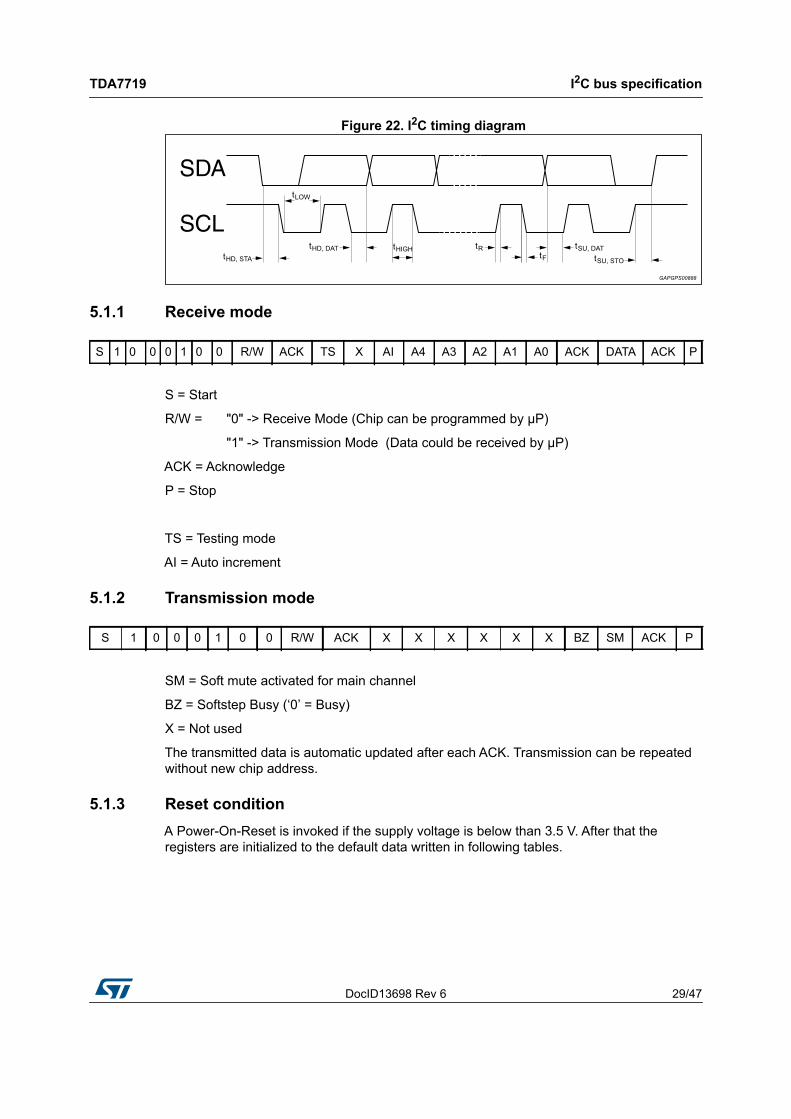
Figure 22. I2C timing diagram
5.1.1 Receive mode
S = Start
R/W = "0" -> Receive Mode (Chip can be programmed by μP)
"1" -> Transmission Mode (Data could be received by μP)
ACK = Acknowledge
P = Stop
TS = Testing mode
AI = Auto increment
5.1.2 Transmission mode
SM = Soft mute activated for main channel
BZ = Softstep Busy (‘0’ = Busy)
X = Not used
The transmitted data is automatic updated after each ACK. Transmission can be repeated without new chip address.
5.1.3 Reset conditionA Power-On-Reset is invoked if the supply voltage is below than 3.5 V. After that the registers are initialized to the default data written in following tables.
S 1 0 0 0 1 0 0 R/W ACK TS X AI A4 A3 A2 A1 A0 ACK DATA ACK P
S 1 0 0 0 1 0 0 R/W ACK X X X X X X BZ SM ACK P

I2C bus specification TDA7719
30/47 DocID13698 Rev 6
Table 10. Subaddress (receive mode) MSB LSB
FunctionI2 I1 I0 A4 A3 A2 A1 A0
01
Testing ModeOffOn
x Not used
01
Auto Increment ModeOffOn
0 0 0 0 0 Input Configuration / Main Source Selector
0 0 0 0 1 2nd Source Selector / Direct Path
0 0 0 1 0 Mixing Source / Mixing Gain
0 0 0 1 1 Mix Control / Level Meter / DC Offset Detector Config
0 0 1 0 0 Soft Mute / Others
0 0 1 0 1 Soft Step I
0 0 1 1 0 Soft Step II / DC-detector
0 0 1 1 1 Loudness
0 1 0 0 0 Volume / Output Gain
0 1 0 0 1 Treble
0 1 0 1 0 Middle
0 1 0 1 1 Bass
0 1 1 0 0 Subwoofer / Middle / Bass
0 1 1 0 1 Speaker Attenuator Left Front
0 1 1 1 0 Speaker Attenuator Right Front
0 1 1 1 1 Speaker Attenuator Left Rear
1 0 0 0 0 Speaker Attenuator Right Rear
1 0 0 0 1 Subwoofer Attenuator Left
1 0 0 1 0 Subwoofer Attenuator Right
1 0 0 1 1 Testing Audio Processor 1
1 0 1 0 0 Testing Audio Processor 2

DocID13698 Rev 6 31/47
TDA7719 I2C bus specification
46
5.2 Data byte specificationThe default power on status of the registers is written with underline.
Note: For detailed input source and input stage configuration, please refer to Section 4.1.
Table 11. Input configuration / main selector (0) MSB LSB
FunctionD7 D6 D5 D4 D3 D2 D1 D0
00001111
00110011
01010101
Main source selectorIN0IN1IN2IN3IN4IN5IN6IN7
01
MD1/2 configuration for main selectorMD1MD2
01
Main source input gain select0dB3dB
00001111
00110011
01010101
Input configurationCFG0CFG1CFG2CFG3CFG4CFG5CFG6CFG7

I2C bus specification TDA7719
32/47 DocID13698 Rev 6
Note: For detailed input source and input stage configuration, please refer to Section 4.1.To active QD3 Bypass (Rear) function, it needs to set Byte3_D4 to “Direct Path / 2nd Source” also.
Table 12. 2nd Source selector / direct path (1) MSB LSB
FunctionD7 D6 D5 D4 D3 D2 D1 D0
00001111
00110011
01010101
2nd Source SelectorIN0IN1IN2IN3IN4IN5IN6IN7
01
MD1/2 Configuration for 2nd SelectorMD1MD2
01
2nd Source Input Gain Select0dB3dB
01
QD2 Bypass (Front)onOff
01
QD3 Bypass (Rear)onOff
01
QD4 Bypass (Subwoofer)onOff

DocID13698 Rev 6 33/47
TDA7719 I2C bus specification
46
Table 13. Mixing source / mixing gain (2) MSB LSB
FunctionD7 D6 D5 D4 D3 D2 D1 D0
00001111
00110011
01010101
Mixing Source SelectorIN0IN1IN2IN3IN4IN5IN6IN7
00000000000000001111111111111111
00000000111111110000000011111111
00001111000011110000111100001111
00110011001100110011001100110011
01010101010101010101010101010101
Mixing Attenuator0dB-1dB-2dB-3dB-4dB-5dB-6dB-7dB-8dB-9dB-10dB-11dB-12dB-13dB-14dB-15dB-16dB-17dB-18dB-19dB-20dB-21dB-22dB-23dB-24dB-25dB-26dB-27dB-28dB-29dB-30dB-31dB

I2C bus specification TDA7719
34/47 DocID13698 Rev 6
Table 14. Mix control / level meter / dc offset detector configure (3) MSB LSB
FunctionD7 D6 D5 D4 D3 D2 D1 D0
01
Mix to Front LeftOnOff
01
Mix to Front RightOnOff
01
Mix to Rear LeftOnOff
01
Mix to Rear RightOnOff
01
Rear Speaker Input ConfigurationDirect Path / 2nd Source Main Signal
01
Reference Output SelectInternal Vref (3.3V)External Vref (4V)
01
Level Meter ResetNormalReset
01
DC Offset Detector / Level Meter ConfigLevel MeterDC Offset Detector

DocID13698 Rev 6 35/47
TDA7719 I2C bus specification
46
Table 15. Soft mute / others (4) MSB LSB
FunctionD7 D6 D5 D4 D3 D2 D1 D0
01
Soft MuteOnOff
01
Pin Influence for MutePin and IICIIC
0011
0101
Soft Mute Time0.48ms0.96ms7.68ms15.36ms
01
Subwoofer Input ConfigurationInput MuxBass Output
01
Subwoofer Enable (OUTL3 & OUTR3)OnOff
01
Fast ChargeOnOff
01
Anti-Alias FilterOnOff (bypass)

I2C bus specification TDA7719
36/47 DocID13698 Rev 6
Table 16. SoftStep I (5) MSB LSB
FunctionD7 D6 D5 D4 D3 D2 D1 D0
01
Loudness Soft StepOnOff
01
Volume Soft StepOnOff
01
Treble Soft StepOnOff
01
Middle Soft StepOnOff
01
Bass Soft StepOnOff
01
Speaker LF Soft StepOnOff
01
Speaker RF Soft StepOnOff
01
Speaker LR Soft StepOnOff

DocID13698 Rev 6 37/47
TDA7719 I2C bus specification
46
Table 17. SoftStep II / DC detector (6) MSB LSB
FunctionD7 D6 D5 D4 D3 D2 D1 D0
01
Speaker RR Soft Steponoff
01
Subwoofer Left Soft Steponoff
01
Subwoofer Right Soft Steponoff
01
Soft Step Time5ms10ms
001
010
Zero-comparator Window size±100mV±75mV±50mV
0011
0101
Spike rejection time constant11μs22 μs33 μs44 μs

I2C bus specification TDA7719
38/47 DocID13698 Rev 6
Table 18. Loudness (7) MSB LSB
FunctionD7 D6 D5 D4 D3 D2 D1 D0
00:11
00:11
00:11
01:01
Attenuation0dB-1dB:-14dB-15dB
0011
0101
Center FrequencyFlat400Hz800Hz2400Hz
01
High Boostonoff
01
Soft Step Actionactwait
Table 19. Volume / output gain (8) MSB LSB
FunctionD7 D6 D5 D4 D3 D2 D1 D0
00:0011:11
00:1111:00
00:1111:00
00:1111:00
01:0110:10
Gain/Attenuation-15dB-14dB:-1dB0dB0dB+1dB:+14dB+15dB
x Not used
01
Output Gain1dB0dB
01
Soft Step Actionactwait

DocID13698 Rev 6 39/47
TDA7719 I2C bus specification
46
Table 20. Treble filter (9) MSB LSB
FunctionD7 D6 D5 D4 D3 D2 D1 D0
00:0011:11
00:1111:00
00:1111:00
00:1111:00
01:0110:10
Gain/Attenuation-15dB-14dB:-1dB0dB0dB+1dB:+14dB+15dB
0011
0101
Treble Center Frequency10.0kHz12.5kHz15.0kHz17.5kHz
01
Soft Step Actionactwait
Table 21. Middle filter (10) MSB LSB
FunctionD7 D6 D5 D4 D3 D2 D1 D0
00:0011:11
00:1111:00
00:1111:00
00:1111:00
01:0110:10
Gain/Attenuation-15dB-14dB:-1dB0dB0dB+1dB:+14dB+15dB
0011
0101
Middle Q Factor0.50.7511.25
01
Soft Step Actionactwait
I2C bus specification TDA7719
40/47 DocID13698 Rev 6
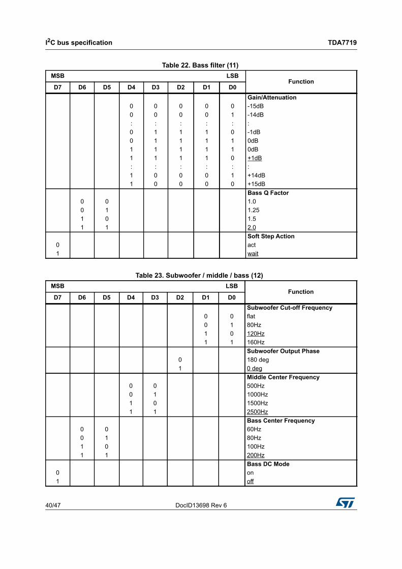
Table 22. Bass filter (11) MSB LSB
FunctionD7 D6 D5 D4 D3 D2 D1 D0
00:0011:11
00:1111:00
00:1111:00
00:1111:00
01:0110:10
Gain/Attenuation-15dB-14dB:-1dB0dB0dB+1dB:+14dB+15dB
0011
0101
Bass Q Factor1.01.251.52.0
01
Soft Step Actionactwait
Table 23. Subwoofer / middle / bass (12) MSB LSB
FunctionD7 D6 D5 D4 D3 D2 D1 D0
0011
0101
Subwoofer Cut-off Frequencyflat80Hz120Hz160Hz
01
Subwoofer Output Phase180 deg0 deg
0011
0101
Middle Center Frequency500Hz1000Hz1500Hz2500Hz
0011
0101
Bass Center Frequency60Hz80Hz100Hz200Hz
01
Bass DC Modeonoff

DocID13698 Rev 6 41/47
TDA7719 I2C bus specification
46
Table 24. Speaker attenuation (LF/RF/LR/RR) (13-16) MSB LSB
FunctionD7 D6 D5 D4 D3 D2 D1 D0
00:000:111
00:000:001
00:011:11x
00:100:11x
00:100:11x
00:100:11x
01:101:01x
Gain/Attenuation0dB0dB:0dB0dB-1dB:-78dB-79dBmute
01
Soft Step Actionactwait
Table 25. Subwoofer attenuation (subwoofer L/subwoofer R) (17-18) MSB LSB
FunctionD7 D6 D5 D4 D3 D2 D1 D0
00:000:111
00:000:001
00:011:11x
00:100:11x
00:100:11x
00:100:11x
01:101:01x
Gain/Attenuation+0dB+1dB:+15dB-0dB-1dB:-78dB-79dBmute
01
Soft Step Actionactwait

I2C bus specification TDA7719
42/47 DocID13698 Rev 6
Table 26. Testing audio processor 1 (19) MSB LSB
FunctionD7 D6 D5 D4 D3 D2 D1 D0
01
Audio Processor Testing Modeoffon
0000000011111111
0000111100001111
0011001100110011
0101010101010101
Test Multiplexer at QD1L (1)
DCDet Vth HighDCDet Vth LowVolumeoutLIntZeroErrInGainLLoudoutLBassoutLMidoutLRef5V5VGB1.26SMCLKTrebleoutLSSCLKClock200kREQSDCLK
01
Clock Fast Mode (2)
onOff
01
Clock Source (2)
external (at mute pin)Internal (200kHz)
x Not Used
1. The control bit needs both I2C test mode on & sub-address test mode on.
2. The control bit does not depend on test mode.

DocID13698 Rev 6 43/47
TDA7719 I2C bus specification
46
Table 27. Testing audio processor 2 (20) MSB LSB
FunctionD7 D6 D5 D4 D3 D2 D1 D0
01
Test Architecture (1)
normalSplit
01
Oscillator Clock (2)
400kHz800kHz
01
Softstep Curve (2)
S-CurveLinear Curve
0011
0101
Manual Set Busy Signal (1)
AutoAuto01
0011
0101
Request for Clk Generator (1)
AllowAllowStoppedStopped
x x x Not Used
1. The control bit needs sub-address test mode on
2. The control bit does not depend on test mode.

Package information TDA7719
44/47 DocID13698 Rev 6
6 Package information
In order to meet environmental requirements, ST offers these devices in different grades of ECOPACK® packages, depending on their level of environmental compliance. ECOPACK® specifications, grade definitions and product status are available at: www.st.com.
ECOPACK® is an ST trademark.
6.1 TSSOP28 package information
Figure 23. TSSOP28 package outline

DocID13698 Rev 6 45/47
TDA7719 Package information
46
Table 28. TSSOP28 package mechanical data
RefDimensions in mm
Min. Typ. Max.
A - - 1.20
A1 0.05 - 0.15
A2 0.80 1.00 1.05
b 0.190 - 0.30
c 0.09 - 0.20
D(1)
1. D and E1 does not include mold flash or protrusions. Mold flash or potrusions shall not exceed 0.15 mm (.006inch) per side.
9.60 9.70 9.80
E 6.20 6.40 6.60
E11 4.30 4.40 4.50
e - 0.65 -
L 0.45 0.60 0.75
L1 - 1.00 -
k 0° (min.), 8° (max.)
aaa - - 0.10

Revision history TDA7719
46/47 DocID13698 Rev 6
7 Revision history
Table 29. Document revision history Date Revision Changes
16-Jul-2007 1 Initial release.
07-Jan-2007 2Added and updated the values on the Table 5: Electrical characteristics.Document status promoted from preliminary data to datasheet.
30-Jul-2008 3 Updated Table 5: Electrical characteristics.
23-Apr-2009 4
Updated Figure 1: Block circuit diagram on page 6.Updated Section 4.1: Input configuration on page 13.Added Section 4.1.2: Direct path on page 15.Added Figure 21: Switching characteristics on page 28, Table 9: I2C bus electrical characteristics on page 28 and Figure 22: I2C timing diagram on page 29.
17-Sep-2013 5 Updated disclaimer.
01-Dec-2017 6
Added “Automotive “ in the title in cover page;Added “AEC-Q100 qualified” as first feature and car icone;Updated Figure 1: Block circuit diagram on page 6;Updated Figure 6: Package information on page 44;Updated disclaimer.

DocID13698 Rev 6 47/47
TDA7719
47
IMPORTANT NOTICE – PLEASE READ CAREFULLY
STMicroelectronics NV and its subsidiaries (“ST”) reserve the right to make changes, corrections, enhancements, modifications, and improvements to ST products and/or to this document at any time without notice. Purchasers should obtain the latest relevant information on ST products before placing orders. ST products are sold pursuant to ST’s terms and conditions of sale in place at the time of order acknowledgement.
Purchasers are solely responsible for the choice, selection, and use of ST products and ST assumes no liability for application assistance or the design of Purchasers’ products.
No license, express or implied, to any intellectual property right is granted by ST herein.
Resale of ST products with provisions different from the information set forth herein shall void any warranty granted by ST for such product.
ST and the ST logo are trademarks of ST. All other product or service names are the property of their respective owners.
Information in this document supersedes and replaces information previously supplied in any prior versions of this document.
© 2017 STMicroelectronics – All rights reserved