Embed Size (px)
Citation preview

Reference Designs for the Broadcast Industry: Volume 3 [optional]
XAPP1015 (v1.0) September 28, 2009 [optional]
Audio/Video Connectivity Solutions for Spartan-3E FPGAsReference Designs for the Broadcast Industry: Volume 3
XAPP1015 (v1.0) September 28, 2009

Spartan-3E FPGAs Audio/Video Connectivity www.xilinx.com XAPP1015 (v1.0) September 28, 2009
Xilinx is disclosing this user guide, manual, release note, and/or specification (the "Documentation") to you solely for use in the development of designs to operate with Xilinx hardware devices. You may not reproduce, distribute, republish, download, display, post, or transmit the Documentation in any form or by any means including, but not limited to, electronic, mechanical, photocopying, recording, or otherwise, without the prior written consent of Xilinx. Xilinx expressly disclaims any liability arising out of your use of the Documentation. Xilinx reserves the right, at its sole discretion, to change the Documentation without notice at any time. Xilinx assumes no obligation to correct any errors contained in the Documentation, or to advise you of any corrections or updates. Xilinx expressly disclaims any liability in connection with technical support or assistance that may be provided to you in connection with the Information.
THE DOCUMENTATION IS DISCLOSED TO YOU “AS-IS” WITH NO WARRANTY OF ANY KIND. XILINX MAKES NO OTHER WARRANTIES, WHETHER EXPRESS, IMPLIED, OR STATUTORY, REGARDING THE DOCUMENTATION, INCLUDING ANY WARRANTIES OF MERCHANTABILITY, FITNESS FOR A PARTICULAR PURPOSE, OR NONINFRINGEMENT OF THIRD-PARTY RIGHTS. IN NO EVENT WILL XILINX BE LIABLE FOR ANY CONSEQUENTIAL, INDIRECT, EXEMPLARY, SPECIAL, OR INCIDENTAL DAMAGES, INCLUDING ANY LOSS OF DATA OR LOST PROFITS, ARISING FROM YOUR USE OF THE DOCUMENTATION.
© 2009 Xilinx, Inc. XILINX, the Xilinx logo, Virtex, Spartan, ISE, and other designated brands included herein are trademarks of Xilinx in the United States and other countries. All other trademarks are the property of their respective owners.
XAPP1015 (v1.0) September 28, 2009 www.xilinx.com Spartan-3E FPGAs Audio/Video Connectivity
Revision HistoryThe following table shows the revision history for this document.
Date Version Revision
09/28/09 1.0 Initial Xilinx release.

Spartan-3E FPGAs Audio/Video Connectivity www.xilinx.com XAPP1015 (v1.0) September 28, 2009
Spartan-3E FPGAs Audio/Video Connectivity www.xilinx.com 5XAPP1015 (v1.0) September 28, 2009
Revision History . . . . . . . . . . . . . . . . . . . . . . . . . . . . . . . . . . . . . . . . . . . . . . . . . . . . . . . . . . . . . 3
Preface: About This GuideGuide Contents . . . . . . . . . . . . . . . . . . . . . . . . . . . . . . . . . . . . . . . . . . . . . . . . . . . . . . . . . . . . . . 9
Section I: DVB-ASI Using Spartan-3E FPGA SelectIO LVDS . . . . . . . . . . . . . . . . . . . . . 9Section II: SD-SDI Using Spartan-3E FPGA SelectIO LVDS . . . . . . . . . . . . . . . . . . . . . . 9
References . . . . . . . . . . . . . . . . . . . . . . . . . . . . . . . . . . . . . . . . . . . . . . . . . . . . . . . . . . . . . . . . . . . 9Additional Resources . . . . . . . . . . . . . . . . . . . . . . . . . . . . . . . . . . . . . . . . . . . . . . . . . . . . . . . 10Conventions . . . . . . . . . . . . . . . . . . . . . . . . . . . . . . . . . . . . . . . . . . . . . . . . . . . . . . . . . . . . . . . . 10
Typographical . . . . . . . . . . . . . . . . . . . . . . . . . . . . . . . . . . . . . . . . . . . . . . . . . . . . . . . . . . . . 10Online Document . . . . . . . . . . . . . . . . . . . . . . . . . . . . . . . . . . . . . . . . . . . . . . . . . . . . . . . . . 11
Section I: DVB-ASI Using Spartan-3E FPGA SelectIO LVDS
Chapter 1: DVB-ASI Introduction and Layer 0 ImplementationBackground . . . . . . . . . . . . . . . . . . . . . . . . . . . . . . . . . . . . . . . . . . . . . . . . . . . . . . . . . . . . . . . . . 15DVB-ASI . . . . . . . . . . . . . . . . . . . . . . . . . . . . . . . . . . . . . . . . . . . . . . . . . . . . . . . . . . . . . . . . . . . 15
Layer 2 . . . . . . . . . . . . . . . . . . . . . . . . . . . . . . . . . . . . . . . . . . . . . . . . . . . . . . . . . . . . . . . . . . 16Layer 1 . . . . . . . . . . . . . . . . . . . . . . . . . . . . . . . . . . . . . . . . . . . . . . . . . . . . . . . . . . . . . . . . . . 17Layer 0 . . . . . . . . . . . . . . . . . . . . . . . . . . . . . . . . . . . . . . . . . . . . . . . . . . . . . . . . . . . . . . . . . . 18
Implementing DVB-ASI Layer 0 Using SelectIO Technology. . . . . . . . . . . . . . . . . 19DVB-ASI Receiver Implementation Using SelectIO Interface . . . . . . . . . . . . . . . . . . . . 19DVB-ASI Transmitter Implementation Using SelectIO Technology . . . . . . . . . . . . . . 20
Conclusion. . . . . . . . . . . . . . . . . . . . . . . . . . . . . . . . . . . . . . . . . . . . . . . . . . . . . . . . . . . . . . . . . . 21
Chapter 2: DVB-ASI Layer 1 and 2 ReceiverSummary . . . . . . . . . . . . . . . . . . . . . . . . . . . . . . . . . . . . . . . . . . . . . . . . . . . . . . . . . . . . . . . . . . . 23ASI Receiver . . . . . . . . . . . . . . . . . . . . . . . . . . . . . . . . . . . . . . . . . . . . . . . . . . . . . . . . . . . . . . . . 23
Data Recovery Unit . . . . . . . . . . . . . . . . . . . . . . . . . . . . . . . . . . . . . . . . . . . . . . . . . . . . . . . 24Deserializer . . . . . . . . . . . . . . . . . . . . . . . . . . . . . . . . . . . . . . . . . . . . . . . . . . . . . . . . . . . . . . 26ASI Parallel Framer . . . . . . . . . . . . . . . . . . . . . . . . . . . . . . . . . . . . . . . . . . . . . . . . . . . . . . . 268B/10B Decoder . . . . . . . . . . . . . . . . . . . . . . . . . . . . . . . . . . . . . . . . . . . . . . . . . . . . . . . . . . 27Link Controller . . . . . . . . . . . . . . . . . . . . . . . . . . . . . . . . . . . . . . . . . . . . . . . . . . . . . . . . . . . 28Rate-Matching FIFO (Comma Correction) . . . . . . . . . . . . . . . . . . . . . . . . . . . . . . . . . . . . 29Clock Generation . . . . . . . . . . . . . . . . . . . . . . . . . . . . . . . . . . . . . . . . . . . . . . . . . . . . . . . . . 32
Reference Design . . . . . . . . . . . . . . . . . . . . . . . . . . . . . . . . . . . . . . . . . . . . . . . . . . . . . . . . . . . 32Design Hierarchy . . . . . . . . . . . . . . . . . . . . . . . . . . . . . . . . . . . . . . . . . . . . . . . . . . . . . . . . . 32DVB-ASI Receiver Ports . . . . . . . . . . . . . . . . . . . . . . . . . . . . . . . . . . . . . . . . . . . . . . . . . . . 33FPGA Resource Usage . . . . . . . . . . . . . . . . . . . . . . . . . . . . . . . . . . . . . . . . . . . . . . . . . . . . . 34
Implementation . . . . . . . . . . . . . . . . . . . . . . . . . . . . . . . . . . . . . . . . . . . . . . . . . . . . . . . . . . . . . 35
Table of Contents

6 www.xilinx.com Spartan-3E FPGAs Audio/Video ConnectivityXAPP1015 (v1.0) September 28, 2009
Generating the Rate-Matching SelectRAM Memory FIFO . . . . . . . . . . . . . . . . . . . . . . 35Conclusion. . . . . . . . . . . . . . . . . . . . . . . . . . . . . . . . . . . . . . . . . . . . . . . . . . . . . . . . . . . . . . . . . . 36
Chapter 3: DVB-ASI Layer 1 and 2 TransmitterSummary . . . . . . . . . . . . . . . . . . . . . . . . . . . . . . . . . . . . . . . . . . . . . . . . . . . . . . . . . . . . . . . . . . . 37ASI Transmitter . . . . . . . . . . . . . . . . . . . . . . . . . . . . . . . . . . . . . . . . . . . . . . . . . . . . . . . . . . . . . 37
8B/10B Encoder . . . . . . . . . . . . . . . . . . . . . . . . . . . . . . . . . . . . . . . . . . . . . . . . . . . . . . . . . . 37Serializer . . . . . . . . . . . . . . . . . . . . . . . . . . . . . . . . . . . . . . . . . . . . . . . . . . . . . . . . . . . . . . . . 38
Clock Generation . . . . . . . . . . . . . . . . . . . . . . . . . . . . . . . . . . . . . . . . . . . . . . . . . . . . . . . . . . . 38Reference Design . . . . . . . . . . . . . . . . . . . . . . . . . . . . . . . . . . . . . . . . . . . . . . . . . . . . . . . . . . . 38
Design Hierarchy . . . . . . . . . . . . . . . . . . . . . . . . . . . . . . . . . . . . . . . . . . . . . . . . . . . . . . . . . 38FPGA Resource Usage . . . . . . . . . . . . . . . . . . . . . . . . . . . . . . . . . . . . . . . . . . . . . . . . . . . . . 39
Conclusion. . . . . . . . . . . . . . . . . . . . . . . . . . . . . . . . . . . . . . . . . . . . . . . . . . . . . . . . . . . . . . . . . . 39
Chapter 4: DVB-ASI Layer 1 and 2 Pass-through Demonstration DesignSummary . . . . . . . . . . . . . . . . . . . . . . . . . . . . . . . . . . . . . . . . . . . . . . . . . . . . . . . . . . . . . . . . . . . 41Reference Design . . . . . . . . . . . . . . . . . . . . . . . . . . . . . . . . . . . . . . . . . . . . . . . . . . . . . . . . . . . 41
Design Hierarchy . . . . . . . . . . . . . . . . . . . . . . . . . . . . . . . . . . . . . . . . . . . . . . . . . . . . . . . . . 43FPGA Resource Usage . . . . . . . . . . . . . . . . . . . . . . . . . . . . . . . . . . . . . . . . . . . . . . . . . . . . . 44Implementation . . . . . . . . . . . . . . . . . . . . . . . . . . . . . . . . . . . . . . . . . . . . . . . . . . . . . . . . . . 45Generating the Rate-Matching SelectRAM Memory FIFO . . . . . . . . . . . . . . . . . . . . . . 45
Running the Demonstration Design . . . . . . . . . . . . . . . . . . . . . . . . . . . . . . . . . . . . . . . . . 46Required Equipment . . . . . . . . . . . . . . . . . . . . . . . . . . . . . . . . . . . . . . . . . . . . . . . . . . . . . . 46Setup Instructions . . . . . . . . . . . . . . . . . . . . . . . . . . . . . . . . . . . . . . . . . . . . . . . . . . . . . . . . 46
Design Summary. . . . . . . . . . . . . . . . . . . . . . . . . . . . . . . . . . . . . . . . . . . . . . . . . . . . . . . . . . . . 47Conclusion. . . . . . . . . . . . . . . . . . . . . . . . . . . . . . . . . . . . . . . . . . . . . . . . . . . . . . . . . . . . . . . . . . 50
Section II: SD-SDI Using Spartan-3E FPGA SelectIO LVDS
Chapter 5: SD-SDI LVDS ReceiverSummary . . . . . . . . . . . . . . . . . . . . . . . . . . . . . . . . . . . . . . . . . . . . . . . . . . . . . . . . . . . . . . . . . . . 53LVDS SD-SDI Receiver (SDI Receiver) . . . . . . . . . . . . . . . . . . . . . . . . . . . . . . . . . . . . . . 53
Data Recovery Unit . . . . . . . . . . . . . . . . . . . . . . . . . . . . . . . . . . . . . . . . . . . . . . . . . . . . . . . 53Deserializer . . . . . . . . . . . . . . . . . . . . . . . . . . . . . . . . . . . . . . . . . . . . . . . . . . . . . . . . . . . . . . 55Video Decoder . . . . . . . . . . . . . . . . . . . . . . . . . . . . . . . . . . . . . . . . . . . . . . . . . . . . . . . . . . . 56EDH Processor . . . . . . . . . . . . . . . . . . . . . . . . . . . . . . . . . . . . . . . . . . . . . . . . . . . . . . . . . . . 56
Clocking . . . . . . . . . . . . . . . . . . . . . . . . . . . . . . . . . . . . . . . . . . . . . . . . . . . . . . . . . . . . . . . . . . . . 56Module I/O . . . . . . . . . . . . . . . . . . . . . . . . . . . . . . . . . . . . . . . . . . . . . . . . . . . . . . . . . . . . . . . . . 57Reference Design . . . . . . . . . . . . . . . . . . . . . . . . . . . . . . . . . . . . . . . . . . . . . . . . . . . . . . . . . . . 58Conclusion. . . . . . . . . . . . . . . . . . . . . . . . . . . . . . . . . . . . . . . . . . . . . . . . . . . . . . . . . . . . . . . . . . 58
Chapter 6: SD-SDI LVDS TransmitterSummary . . . . . . . . . . . . . . . . . . . . . . . . . . . . . . . . . . . . . . . . . . . . . . . . . . . . . . . . . . . . . . . . . . . 59

Spartan-3E FPGAs Audio/Video Connectivity www.xilinx.com 7XAPP1015 (v1.0) September 28, 2009
SD-SDI Transmitter . . . . . . . . . . . . . . . . . . . . . . . . . . . . . . . . . . . . . . . . . . . . . . . . . . . . . . . . . 59Video Pattern Generator . . . . . . . . . . . . . . . . . . . . . . . . . . . . . . . . . . . . . . . . . . . . . . . . . . . 60Standard Detect and Flywheel . . . . . . . . . . . . . . . . . . . . . . . . . . . . . . . . . . . . . . . . . . . . . . 60Ancillary Data/EDH Processor . . . . . . . . . . . . . . . . . . . . . . . . . . . . . . . . . . . . . . . . . . . . . 61Video Encoder . . . . . . . . . . . . . . . . . . . . . . . . . . . . . . . . . . . . . . . . . . . . . . . . . . . . . . . . . . . 62Serializer . . . . . . . . . . . . . . . . . . . . . . . . . . . . . . . . . . . . . . . . . . . . . . . . . . . . . . . . . . . . . . . . 62
Clocking . . . . . . . . . . . . . . . . . . . . . . . . . . . . . . . . . . . . . . . . . . . . . . . . . . . . . . . . . . . . . . . . . . . . 62Module I/O . . . . . . . . . . . . . . . . . . . . . . . . . . . . . . . . . . . . . . . . . . . . . . . . . . . . . . . . . . . . . . . . . 62Reference Design . . . . . . . . . . . . . . . . . . . . . . . . . . . . . . . . . . . . . . . . . . . . . . . . . . . . . . . . . . . 65Conclusion. . . . . . . . . . . . . . . . . . . . . . . . . . . . . . . . . . . . . . . . . . . . . . . . . . . . . . . . . . . . . . . . . . 65
Chapter 7: SD-SDI Receiver/Transmitter Demonstration DesignSummary . . . . . . . . . . . . . . . . . . . . . . . . . . . . . . . . . . . . . . . . . . . . . . . . . . . . . . . . . . . . . . . . . . . 67Reference Design . . . . . . . . . . . . . . . . . . . . . . . . . . . . . . . . . . . . . . . . . . . . . . . . . . . . . . . . . . . 67Spartan-3E FPGA SDI Demonstration Board. . . . . . . . . . . . . . . . . . . . . . . . . . . . . . . . . 68
Spartan-3E FPGA SDI Receiver Demonstration . . . . . . . . . . . . . . . . . . . . . . . . . . . . . . . 68Spartan-3E FPGA SDI Transmitter Demonstration . . . . . . . . . . . . . . . . . . . . . . . . . . . . 72

8 www.xilinx.com Spartan-3E FPGAs Audio/Video ConnectivityXAPP1015 (v1.0) September 28, 2009

Spartan-3E FPGAs Audio/Video Connectivity www.xilinx.com 9XAPP1015 (v1.0) September 28, 2009
Preface
About This Guide
This application note describes how to use Spartan®-3E FPGAs to implement various serial digital video interfaces commonly used in the professional video broadcast industry.
Guide ContentsThis document contains the following sections and chapters:
Section I: DVB-ASI Using Spartan-3E FPGA SelectIO LVDS• Chapter 1, “DVB-ASI Introduction and Layer 0 Implementation” introduces DVB-ASI
and provides an implementation guide for layer 0.
• Chapter 2, “DVB-ASI Layer 1 and 2 Receiver” presents a DVB-ASI receiver design for the Spartan-3E FPGA that uses the Xilinx® SelectIO™ technology.
• Chapter 3, “DVB-ASI Layer 1 and 2 Transmitter” presents a DVB-ASI transmitter design for the Spartan-3E FPGA that uses the Xilinx SelectIO technology.
• Chapter 4, “DVB-ASI Layer 1 and 2 Pass-through Demonstration Design” presents a DVB-ASI pass-through design for the Spartan-3E FPGA that uses the Xilinx SelectIO technology.
Section II: SD-SDI Using Spartan-3E FPGA SelectIO LVDS• Chapter 5, “SD-SDI LVDS Receiver” describes an SD-SDI receiver reference design for
Spartan-3E FPGAs.
• Chapter 6, “SD-SDI LVDS Transmitter” describes an SD-SDI transmitter reference design for Spartan-3E FPGAs.
• Chapter 7, “SD-SDI Receiver/Transmitter Demonstration Design” describes an SD-SDI combined receiver and transmitter demonstration design for Spartan-3E FPGAs.
ReferencesThis application note uses the following references:
1. EN 50083-9, Cabled Distribution Systems for Television, Sound and Interactive Multimedia Signals, http://www.dvb.org.
2. ISO/IEC 13818-1:2007, Information technology — Generic coding of moving pictures and associated audio information: Systems, International Organization for Standardization, http://www.iso.org/iso/catalogue_detail.htm?csnumber=44169.

10 www.xilinx.com Spartan-3E FPGAs Audio/Video ConnectivityXAPP1015 (v1.0) September 28, 2009
Preface: About This Guide
3. Widmer, A. X., and P. A. Franaszek. A DC-Balanced, Partitioned-Block, 8B/10B Transmission Code (IBM Journal of Research and Development, Vol. 27, Number 5, 1983).
4. XAPP514, Audio/Video Connectivity Solutions for Virtex®-II Pro and Virtex-4 FPGAs.
Additional ResourcesTo find additional documentation, see the Xilinx website at:
http://www.xilinx.com/support/documentation/index.htm.
To search the Answer Database of silicon, software, and IP questions and answers, or to create a technical support WebCase, see the Xilinx website at:
http://www.xilinx.com/support/mysupport.htm.
ConventionsThis document uses the following conventions. An example illustrates each convention.
TypographicalThe following typographical conventions are used in this document:
Convention Meaning or Use Example
Courier fontMessages, prompts, and program files that the system displays
speed grade: - 100
Courier boldLiteral commands that you enter in a syntactical statement
ngdbuild design_name
Helvetica bold
Commands that you select from a menu
File → Open
Keyboard shortcuts Ctrl+C
Italic font
Variables in a syntax statement for which you must supply values
ngdbuild design_name
References to other manualsSee the Development System Reference Guide for more information.
Emphasis in textIf a wire is drawn so that it overlaps the pin of a symbol, the two nets are not connected.
Square brackets [ ]
An optional entry or parameter. However, in bus specifications, such as bus[7:0], they are required.
ngdbuild [option_name] design_name
Braces { }A list of items from which you must choose one or more
lowpwr ={on|off}
Vertical bar |Separates items in a list of choices
lowpwr ={on|off}

Spartan-3E FPGAs Audio/Video Connectivity www.xilinx.com 11XAPP1015 (v1.0) September 28, 2009
Conventions
Online DocumentThe following conventions are used in this document:
Vertical ellipsis...
Repetitive material that has been omitted
IOB #1: Name = QOUT’ IOB #2: Name = CLKIN’...
Horizontal ellipsis . . .Repetitive material that has been omitted
allow block block_name loc1 loc2 ... locn;
Convention Meaning or Use Example
Convention Meaning or Use Example
Blue textCross-reference link to a location in the current document
See the section “Additional Resources” for details.
Refer to “Title Formats” in Chapter 1 for details.
Blue, underlined text Hyperlink to a website (URL)Go to http://www.xilinx.com for the latest speed files.

12 www.xilinx.com Spartan-3E FPGAs Audio/Video ConnectivityXAPP1015 (v1.0) September 28, 2009
Preface: About This Guide

Reference Designs for the Broadcast Industry: Volume 3 [optional]
XAPP1015 (v1.0) September 28, 2009 [optional]
Section I:DVB-ASI Using Spartan-3E FPGA SelectIO LVDSAudio/Video Connectivity Solutions for Spartan-3E FPGAs

Spartan-3E FPGAs Audio/Video Connectivity www.xilinx.com XAPP1015 (v1.0) September 28, 2009

Spartan-3E FPGAs Audio/Video Connectivity www.xilinx.com 15XAPP1015 (v1.0) September 28, 2009
Chapter 1
DVB-ASI Introduction and Layer 0 Implementation
BackgroundDigital Video Broadcast (DVB) is the result of a large-scale cooperative effort by numerous commercial manufacturers, television network operators, broadcasters, and others to provide a uniform set of standards for digital television and data services. DVB has proven highly successful, with over 150 million DVB receivers deployed.
Late in 1991, at the beginning of digital television deployment, industry-leading manufacturers, broadcasters, and regulatory bodies formed the European Launching Group to guide and manage the technology requirements for digital media services. In 1993, a memorandum of understanding was signed by all participants, and the DVB project was born.
DVB immediately addressed the critical need for standards required to deliver digital media content via the traditional broadcast networks. The three key standards introduced during this period were DVB-Satellite (DVB-S), DVB-Cable (DVB-C), and DVB-Terrestrial (DVB-T). These standards have been widely adopted in Europe, Australia, and Asia. DVB-S forms the basis for satellite televisions almost everywhere. DVB-C is the most common cable system format, and DVB-T is increasing in popularity.
Other supporting standards are needed for service information, subtitling, and interfacing. DVB Asynchronous Serial Interface (DVB-ASI) is one such standard. It is one of three primary interfaces prescribed for the transmission and reception of MPEG-2 compressed data signals. This interface is specified in detail in European Standard EN 50083-9 [Ref 1], originally approved by Cenelec in 1996.
DVB-ASIThe DVB-ASI standard describes a system interface for encoded, serial transmission of different data rates using a constant transmission rate. The standard is based on a three-layer structure. The top layer (layer 2) uses MPEG transport packets as described in EN/ISO/IEC 13818-1 [Ref 2]. The bottom two layers (layers 1 and 0) are based on the Fibre Channel standard ISE/IEC/CD 141165-1, part 1.
While Fibre Channel specifications form the basis for this interface, DVB-ASI is not restricted to fiber as a transmission medium. The interface described in this chapter uses standard 75Ω copper coaxial cable, as defined in the DVB-ASI standard. Figure 1-1 shows the DVB-ASI layered structure.

16 www.xilinx.com Spartan-3E FPGAs Audio/Video ConnectivityXAPP1015 (v1.0) September 28, 2009
Chapter 1: DVB-ASI Introduction and Layer 0 Implementation
Each of the layers comprises different physical and logical aspects of the interface. Figure 1-2 shows how each layer of the DVB-ASI standard maps to a generic design implementation.
Layer 2Layer 2 represents the MPEG-2 transport stream. This transport stream is not part of the layer 1/layer 0 implementations that are discussed in other chapters. The MPEG-2 transport stream is composed of MPEG-2 packets that can be either 188 bytes (for standard transmission), or 204 bytes (when the packets are Reed-Solomon encoded for forward error correction.) These packets are passed one byte at a time to layer 1. Figure 1-3 shows the format of a basic DVB-ASI MPEG transport packet. The DVB-ASI specification requires every MPEG transport packet to be separated by special comma characters (also referred to as sync bytes). These sync bytes, represented by the value 0xBC, enable synchronization within one MPEG packet. At least two sync bytes must separate each MPEG packet. For more detail on sync bytes see “Layer 1,” page 17.
X-Ref Target - Figure 1-1
Figure 1-1: DVB-ASI Layered Protocol
X-Ref Target - Figure 1-2
Figure 1-2: DVB-ASI Generic Design Implementation
Layer 0: Physical Layer
Layer 1: Data Encoding
Layer 2: MPEG Transport Layer
X1015_c1_01_051909
MPEG-2 Packets
Sync Byte Insertion
8B/10B Encoding Serializer
ASI Driver
Cable Equalizer
Sync Byte Deletion
8B/10B Decoding
Data Recovery and Deserializer
MPEG-2 Packets
Layer 1 TX
Layer 1 RX
X1015_c1_02_060109
Layer 1 Layer 0Layer 2

Spartan-3E FPGAs Audio/Video Connectivity www.xilinx.com 17XAPP1015 (v1.0) September 28, 2009
DVB-ASI
Aside from the requirement that two sync bytes separate packets, there are no rules governing how packets are sent. It is common for an MPEG-2 transport stream to contain many sync bytes in addition to the minimum two. This is possible because the full transport stream bandwidth might not be needed. For example, if the user sends a 10 Mb/s stream on a single DVB-ASI channel, 206 Mb/s is still available. If no packet data is available, the specification calls for a transmitter (TX) to just send sync bytes.
Layer 1In the transmitter, layer 1 defines sync byte insertion, 8B/10B encoding, and data serialization. In the receiver (RX), layer 1 defines data recovery and deserialization, 8B/10B decoding, and sync byte deletion.
The first step in the transmitter is to insert sync bytes into the MPEG transport stream for byte synchronization. Byte synchronization is necessary because the receiver samples the input asynchronously.
To align data on word boundaries, the encoding scheme encodes sync bytes with special patterns guaranteed not to occur in the input data. These patterns allow the receiver to determine the offset of the incoming data relative to the correct word boundaries. The sync byte used in DVB-ASI is the K28.5 word (defined in the 8B/10B codes), which decodes to an 8-bit value of 0xBC. Because this is also a valid 8-bit data value, the encoder has a special input flag that causes the 8-bit word to encode differently if it is a sync byte. In general, the byte synchronization pattern consists of two sync bytes within a 5-byte window. A common pattern is two successive sync bytes.
After sync byte insertion, the data stream is sent to the encoder. Here, it is encoded with a DC-balanced 8B/10B transmission code. 8B/10B codes are transition rich (run length limited) and have minimal DC offset. They also provide some basic error detection by detecting invalid 10-bit code words (code error), and by tracking and enforcing the notion of running disparity (disparity error). Running disparity computes the difference in the number of ones and zeros present in the current and subsequent 10-bit code words, and enforces this difference to be either positive or negative.
A complete discussion of 8B/10B codes is beyond the scope of this chapter, but a complete description of the code is available in technical publications [Ref 3].
After it is encoded, the 10-bit data is serialized using a 10:1 serializer. The serializer shifts one bit per clock at a line rate of 270 Mb/s. The actual payload bandwidth, however, is 216 Mb/s, because the 8B/10B block code uses 10 bits to encode each byte of 8 bits, thereby incurring a 20% overhead penalty.
In the receiver, the first step is data recovery. This is done with a clock and data recovery circuit using a phase-locked loop (PLL) or oversampling data recovery unit. Next, the data is deserialized and decoded from 10 bits to 8 bits using the 8B/10B codes. Code and disparity errors are detected at this point.
X-Ref Target - Figure 1-3
Figure 1-3: MPEG Transport Packet Format
Comma Character
BC BC 47 48 49 90 91 92
0 1 2 185 186 187
Comma Character Packet Header
Sync Byte Sync Byte Start ofPacket
187 Bytes Make Up MPEG-2Compliant Packet
X1015_c1_03_051909
...

18 www.xilinx.com Spartan-3E FPGAs Audio/Video ConnectivityXAPP1015 (v1.0) September 28, 2009
Chapter 1: DVB-ASI Introduction and Layer 0 Implementation
The deserialized data is then sent for comma (sync byte) detection. In this step, the receiver searches the incoming data stream for sync bytes. After the sync byte pattern is detected, an offset is calculated that indicates the amount of rotation needed in the data words to properly align them on word boundaries.
In general, the exact location of these byte-synchronizing characters is unimportant because, other than for synchronization purposes, they are ignored by the receiver. Lastly, sync bytes are deleted from the stream.
Comma Correction
In some instances, a layer 2 design might require data to be extracted from the receiver at a rate faster or slower than the incoming bit rate. Because DVB-ASI uses a streaming interface and no handshaking can take place, the receiver uses a scheme called comma, or sync byte, correction. In this scheme, the receiver uses an elastic memory buffer and inserts or deletes sync bytes as needed to match the transmitter rate to the receiver rate. This method allows the layer 2 implementation to extract data from layer 1 at a convenient clock rate. For example, the incoming data rate can be, on average, 27 MHz. The layer 2 implementation can use a 33 MHz clock, if necessary. By using comma correction, the layer 2 implementation can clock data from the receiver at this faster rate without underflowing the receiver and getting corrupted data. The layer 2 implementation reads and discards additional sync bytes until it sees actual data as indicated by the receiver. Conversely, if the layer 2 implementation runs at a rate slower than the receiver, layer 1 deletes sync bytes as needed to prevent overflow and lost data. Only sync bytes can be inserted or deleted because they are ignored by the layer 2 implementation.
Layer 0Layer 0, the physical layer of the protocol, addresses jitter performance, line rates, bit timing, receiver timing acquisition, and electrical medium characteristics. While both optical and copper transmission media are supported by the standard, this chapter deals only with the copper coaxial cable interface.
Jitter in coaxial applications is specified by random jitter (RJ), deterministic jitter (DJ, also known as data-dependent jitter), and duty cycle distortion. Specified as peak-to-peak values, the DJ component should be no more than 10% of the line rate unit interval (UI). RJ should be no more than 8% of the UI.
Line rates are 270 Mb/s. Receivers might not recover the clock from the encoded bitstream in addition to the data. In the examples described in this chapter, only data recovery is implemented. The line rate is specified as 270 Mb/s ± 100 ppm.
Receiver timing acquisition is the amount of time required for the ASI receiver to synchronize or bit align to the incoming data stream. This is different from the byte synchronization process discussed in “Layer 1,” page 17. Bit alignment is the notion of sampling a data bit in the valid region, avoiding edges and metastability. In PLL-based systems, receiver timing acquisition includes the time for the PLL to lock onto the clock embedded in the data and sample the incoming serial data. In asynchronous sampled systems, such as those discussed here, receiver acquisition time is a function of the design of the receiver data sampling and recovery circuit. The specification requires the receiver acquisition time to be less than or equal to 1 ms.
The electrical characteristics for a copper coaxial interface specify a nominal cable impedance of 75Ω. BNC connectors are recommended for their mechanical robustness. Detailed electrical specifications can be found in European Standard EN 50083-9 [Ref 1].

Spartan-3E FPGAs Audio/Video Connectivity www.xilinx.com 19XAPP1015 (v1.0) September 28, 2009
Implementing DVB-ASI Layer 0 Using SelectIO Technology
Implementing DVB-ASI Layer 0 Using SelectIO TechnologyXilinx® FPGAs feature I/O cells with a rich set of programmable standards known as SelectIO™ technology that can be used to implement DVB-ASI. Some external components are required to meet the DVB-ASI electrical specifications. In general, DVB-ASI specifies receiver and transmitter electrical characteristics without specifying the implementation details. These specifications can be met by utilizing techniques commonly used in the digital television serial digital interface (SDI) standard. Receiver inputs are required to use transformer coupling. Cable length requirements are not specified, but practicable cable lengths are similar to those specified for SDI. DVB-ASI uses a differential interface similar to standard low-voltage differential signaling (LVDS).
DVB-ASI Receiver Implementation Using SelectIO InterfaceThe receiver specification is described in EN 50083-9 [Ref 3], which calls for transformer coupling between the receiver and connector. Figure 1-4 illustrates the implementation of DVB-ASI using the Xilinx LVDS_25 I/O standard with internal termination. No external terminating resistor is required. The internal LVDS input buffer with SelectIO technology provides a robust, high-speed LVDS interface for ASI.
The DVB-ASI specification does not specify a cable length requirement. However, it is common for DVB-ASI designs to use SD-SDI coaxial cable length definitions. With its slower bit rates, SD-SDI allows maximum cable lengths of up to 300 meters. The coaxial cable causes frequency-dependent attenuation and phase distortion of the signal, attenuating and phase shifting higher frequency components more than lower frequency components. After passing through a long coaxial cable, the signal is severely distorted and attenuated.
The receiver must compensate for this attenuation and distortion before recovering the signal. Typically, SDI receivers use an adaptive cable length equalizer for this purpose. Such an equalizer actively monitors the amount of attenuation and distortion present on the incoming signal and applies the correct amount of equalization to the signal. The cable length can be changed without requiring a change to the equalizer, as would be the case if fixed-length equalization were used. The SDI specifications call for capacitive coupling between the connector and the receiver. Figure 1-5 illustrates the cable equalizer used on the SD-SDI interface, as implemented on the CTXIL206 SDV demonstration board for the Spartan®-3E FPGA (designed by Cook Technologies).
X-Ref Target - Figure 1-4
Figure 1-4: DVB-ASI Implementation Using Xilinx LVDS_25 I/O Standard
0.1 µF
0.1 µF
ASI-RXBNCInput
ASI_RX_P
ASI_RX_N
To CDR
LVDS Buffer Internally Terminated at 50W X1015_c1_04_08319

20 www.xilinx.com Spartan-3E FPGAs Audio/Video ConnectivityXAPP1015 (v1.0) September 28, 2009
Chapter 1: DVB-ASI Introduction and Layer 0 Implementation
DVB-ASI Transmitter Implementation Using SelectIO TechnologyThe ASI transmitter layer 0 specification calls for transformer coupling between the line driver and connector. While the signaling levels are similar to standard LVDS, the ability to drive long cables is needed. Because of this, the SelectIO interface LVDS buffer cannot be used directly but must be connected to an appropriate cable driver as shown in Figure 1-6.
As with the receiver, it is common practice to implement an ASI transmitter layer 0 interface using the SDI transmitter specifications. This allows the user to implement a multi-standard ASI/SDI output on the same physical connection. The SDI specifications call for capacitive coupling between the line driver and the connector. Figure 1-7 illustrates the cable driver used on the SD-SDI transmitter as implemented on the Cook Technologies, CTXIL206 SDV demonstration board for the Spartan-3E FPGA.
X-Ref Target - Figure 1-5
Figure 1-5: Cable Equalizer for SD-SDI Interface on CTXIL206 Board
GS1574A
SD_DTAIN_P
SD_DTAIN_N
SD_CD#
VCC
SD_MUTE
1316
1110
15
149
1 8
1.5 kΩ
4.7 μF
470 nF
1 μF
1 μF
470 nF
4.7 μF
12
VCC
SDOSDO#
CD#
VEEVEEVEEVEE
AGC+AGC–
SDISDI#
MUTEMCLADJBYPASS
37.5Ω75Ω
75Ω
6.4 nH
0.01 μF
123 5
4
X1015_c1_05_051909
+3.3V
56
23
87
14
X-Ref Target - Figure 1-6
Figure 1-6: Cable Driver for DVB-ASI Transmitter Using SelectIO Interface LVDS Buffer
ASI_TX_P
ASI_TX_N
SelectIO Interface LVDS_25 Buffer
ASI SerialBitstream
RREF 1.91 kW
3.3V
150W100W CLC001
75W 75W
0.1 µF
0.1 µF
SDI TXBNC Output
X1015_c1_06_083109

Spartan-3E FPGAs Audio/Video Connectivity www.xilinx.com 21XAPP1015 (v1.0) September 28, 2009
Conclusion
ConclusionThis chapter introduces DVB-ASI and provides an implementation guide for layer 0. For complete reference designs for layer 1 and layer 2 applications of Xilinx FPGAs, see Chapter 2, “DVB-ASI Layer 1 and 2 Receiver,” Chapter 3, “DVB-ASI Layer 1 and 2 Transmitter,”and Chapter 4, “DVB-ASI Layer 1 and 2 Pass-through Demonstration Design.”
X-Ref Target - Figure 1-7
Figure 1-7: Cable Driver for SD-SDI Interface on CTXIL206 Board
9
1211
3
10
1
1
2
2
4
GS1578A
VCC
SDOPSDON
VEE
SD/HD#
SDIPSDIN
RSET
HD_SD3
SD_DTAOUT_P
SD_DTAOUT_N
1235
4
X1015_c1_07_052909
75Ω
75Ω
4.7 μF
0.01μF
+3.3V
+3.3V+3.3V
750Ω
4.7 μF
0.01 μF
C150
L853-0023-01
5.6 nH
75Ω
5.6 nH
75Ω
75Ω
4.7 μF
4.7 μF
49.9Ω
49.9Ω

22 www.xilinx.com Spartan-3E FPGAs Audio/Video ConnectivityXAPP1015 (v1.0) September 28, 2009
Chapter 1: DVB-ASI Introduction and Layer 0 Implementation

Spartan-3E FPGAs Audio/Video Connectivity www.xilinx.com 23XAPP1015 (v1.0) September 28, 2009
Chapter 2
DVB-ASI Layer 1 and 2 Receiver
SummaryDVB-ASI provides an industry-standard method for transmitting MPEG-2 compressed video over high-speed asynchronous serial interfaces. This chapter presents a DVB-ASI receiver design using a Spartan®-3E FPGA with an LVDS SelectIO™ interface. This design implements a robust 270 MHz Mb/s ASI receiver in a cost-effective manner using advanced techniques, silicon features, and tool capabilities.
Chapter 1, “DVB-ASI Introduction and Layer 0 Implementation” contains valuable information that is used throughout this chapter.
ASI ReceiverFigure 2-1 depicts a block diagram of the ASI receiver design.
X-Ref Target - Figure 2-1
Figure 2-1: ASI Receiver Block Diagram
Link Controller
Clock Generation
8B/10BDecoder
Rate-Matching FIFO
SerialData270 Mb/s
LVDS Input
135 MHz
270 MHz
Comma
Data
User Clk
AsynchronousBoundary
X1015_C2_01_061609
10 810 8FramerDRU DES
54 MHz

24 www.xilinx.com Spartan-3E FPGAs Audio/Video ConnectivityXAPP1015 (v1.0) September 28, 2009
Chapter 2: DVB-ASI Layer 1 and 2 Receiver
Data Recovery UnitThe data recovery unit (DRU) samples the incoming serial data asynchronously using a 4-phase DDR sampling method. This method yields an 8X oversampling of the input stream sufficient to provide reliable data acquisition at 270 Mb/s. The DRU is clocked at 270 MHz. Four clock phases (0°, 45°, 90°, and 135°), each clocking two sampling flip-flops (positive and negative edge triggered), provide a total of two sample points per clock phase, 180° apart. This gives a total of eight sample points per bit interval.
The output of each sample pair is double-registered to prevent metastability. A state machine examines the resulting samples, and determines edge positions as well as which registers contain valid data samples. The correctly chosen samples are then output from the DRU at a rate of zero, one, or two bits per clock, depending on the sample point. A 2-bit data valid output indicates when the data is valid as well as how many bits should be shifted for deserialization as discussed in “Deserializer,” page 26.
Implementation of the high-speed 270 MHz circuitry in a Spartan device requires the use of advanced design techniques and Xilinx® tool capabilities. To meet timing consistently, this portion of the ASI receiver utilizes relationally placed macros (RPMs) and directed routing. RPMs provide a method of preserving the relative placement of components to allow the macro to be relocated (manually or automatically), while preserving design performance. Directed routing is an advanced tool feature that preserves the routing of individual nets, regardless of implementation runs or parameters. Directed routing allows the high-performance block to be relocated to other areas on the device as needed while preserving performance.
DRU Advanced Implementation
This section contains advanced information and assumes familiarity with RPMs, directed routing, and the routing details of the target FPGA architecture. The source files (DRU.v/vhd) should be referred to when studying this section.
As discussed in “Data Recovery Unit,” the DRU uses eight sample flip-flops to provide the 8X oversampling of the input. In order for the 8X oversampling and data recovery to work correctly, the sample points need to be equally spaced within the sample window. To ensure this, the 8-sample flip-flops utilize relative placement constraints to lock the flip-flop placement relative to the I/O and to each other. This enables a low-skew route of the input net to each sample flip-flop. Figure 2-2, page 25 shows the placement of these sample flip-flops in a Spartan-3E FPGA 3S1600E. This relative placement allows the designer to manage routing delays to each sample flip-flop with minimal skew. The eight primary sampling flip-flops are denoted QR, QR0, QR1, and QR2 for the rising-edge samples, and QF, QF0, QF1, and QF2 for the falling-edge samples. Figure 2-2, page 25 shows the slices highlighted for each of these flip-flop locations. In some cases, additional flip-flops for metastability are included in the RPM within these slices.
In addition to the relative placement and to preserve performance between iterative implementations of the design, directed routing constraints are applied to the routing from the LVDS input pads to the eight sampling flip-flops. Directed routing is a way to preserve routing, down to the exact wire, regardless of the implementation settings, and ensures that the sampling flip-flops always work correctly. This design contains a total of 13 directed routes. The directed routing strings are first extracted using FPGA Editor. These strings are then used in the VHDL code so that each time the design is synthesized, these special routing directives are embedded into the resulting synthesis netlist and are preserved all the way through to the bitstream.

Spartan-3E FPGAs Audio/Video Connectivity www.xilinx.com 25XAPP1015 (v1.0) September 28, 2009
ASI Receiver
During the routing phase of the implementation, place and route (PAR) provides the following feedback in the route report indicating whether or not the directed routes were successful:
"Starting Router
# of EXACT MODE DIRECTED ROUTING found:13, SUCCESS:13, FAILED:0"
If the status above indicates any failed routes, a problem was encountered during the routing phase, and it should not be assumed that the circuit will function properly.
In Figure 2-2, the asi_datain net is highlighted to show the critical routes that require directed routing constraints. The directed routing attribute for this net is shown in the top-level design file and must be preserved to maintain the low-skew route. Additional directed routing strings, along with the relative location (RLOC) constraints for the RPM, are found in the source file DRU.v/vhd. The RLOC_ORIGIN constraint to locate the RPM on the FPGA grid is set in the UCF file included with the reference design.
X-Ref Target - Figure 2-2
Figure 2-2: DRU Sample Flip-Flops and Input
X1015_c2_02_051909

26 www.xilinx.com Spartan-3E FPGAs Audio/Video ConnectivityXAPP1015 (v1.0) September 28, 2009
Chapter 2: DVB-ASI Layer 1 and 2 Receiver
DeserializerIn high-speed serial communications systems, it is necessary for practical reasons to convert the high-frequency bit rate of the incoming serial data to a more manageable frequency. The deserializer (DES) provides this function. In essence, the deserializer is a serial-to-parallel converter. In its simplest form, it converts the single-bit serial input stream into a multiple-bit parallel word and a parallel clock rate inversely proportional to the number of bits in the parallel word. This conversion from the serial rate to the parallel rate is generally expressed as a ratio. For example, a 1:8 ratio produces 8-bit words at 1/8th the frequency of the serial bit rate. If the serial input frequency is 320 Mb/s, the deserializer outputs 8-bit words at 40 MHz.
The DVB-ASI receiver deserializer provides a 1:10 ratio. Samples are collected from the DRU at a rate of zero, one, or two bits per serial clock until a 10-bit word is collected. The 10-bit word is output along with a data valid output indicating a valid new word. This signal toggles, on average, at the word clock rate of 27 MHz and is synchronous to the 0° phase 270 MHz clock. As discussed in “Clock Generation,” page 32, a 54 MHz clock is provided for the parallel datapath of the design. The deserializer clock enable is also synchronous to this clock, and all circuitry downstream from the deserializer runs at the 54 MHz rate.
On average, the deserializer generates 10-bit words at a 27 MHz rate. The data valid output therefore toggles, on average, every cycle of the 54 MHz clock. On occasion, due to the asynchronous sampling of the input stream, the deserializer can produce two 10-bit words in a single 54 MHz period.
ASI Parallel FramerFor DVB-ASI, the incoming data is encoded into 10-bit words using 8B/10B encoding rules. Because the input data is sampled asynchronously, the data produced by the DRU might span word boundaries. To align on word boundaries, special patterns guaranteed not to occur in the input data are provided by the encoding scheme. The words, called sync bytes (8B/10B K28.5 symbols), provide a mechanism to determine the offset of the incoming data relative to the correct word boundaries. Refer to Chapter 1, “DVB-ASI Introduction and Layer 0 Implementation” for more information.
The ASI Parallel Framer (framer) searches the incoming data for the sync byte pattern. After the sync byte pattern is detected, an offset is calculated indicating the amount of rotation needed in the data words to properly align them on word boundaries. This offset is fed to a simple barrel shifter that rotates the incoming data to the correct offset, thereby aligning the data on the proper 10-bit boundaries. Because the input data is unframed, the framer uses an aggregate 30-bit word formed from multiple input words for searching. This ensures that the sync byte is found regardless of the offset in the incoming data. To simplify the logic, the framer only needs to search for one of the K28.5 symbols because both are guaranteed to be in the data, as defined by 8B/10B encoding rules.
Figure 2-3 illustrates this concept. Most 8B/10B codes are balanced (i.e., they have the same number of ones and zeros in each 10-bit symbol.) However, for codes that are not balanced, there are two code word outputs for the same input. These outputs are complements of one another and serve to maintain the correct running disparity (see the “8B/10B Encoder” section of Chapter 3, “DVB-ASI Layer 1 and 2 Transmitter” for details). The data shown in Figure 2-3 are alternating K28.5 sync bytes (0101111100 and 1010000011). This would be the transmitter output if no MPEG transport stream data were available to send. To maintain the correct running disparity, the encoder transmits one form of the K28.5, and then its complement. In the unframed data, the 10-bit word boundaries are shifted to the right by two bits due to the asynchronous sampling of the

Spartan-3E FPGAs Audio/Video Connectivity www.xilinx.com 27XAPP1015 (v1.0) September 28, 2009
ASI Receiver
data. After framing, the data is rotated to the left to correct the offset, and the sync bytes are properly framed.
Generally, the framer frames the input once on start-up, but the ASI framer also supports reframing. Reframes are issued due to an error condition or because the user is asserting the request externally. A reframe forces the framer to reacquire the sync byte pattern in the data and recalculate the offset. The link controller is used to issue this reframe. For more information, refer to “Link Controller,” page 28.
8B/10B DecoderDVB-ASI streams carry MPEG-2 compressed video data using 8B/10B encoding. A complete discussion of 8B/10B encoding is beyond the scope of this application note, but Chapter 1, “DVB-ASI Introduction and Layer 0 Implementation” provides some background.
The 8B/10B decoder takes 10-bit input words and decodes them to 8-bit outputs and a special code indicator output. In the process of decoding, the decoder breaks the 10-bit word into two separate 4-bit and 6-bit words called sub-blocks. These are referred to as the 6B and 4B sub-blocks, respectively. These sub-blocks are used to decode and check for disparity errors. The 6B sub-block is decoded to a 5-bit output, and the 4B sub-block to a 3-bit output. These two results are then combined to form the complete 8-bit output word.
The special code indicator is asserted whenever the 10-bit input word is one of the special K-codes provided by the 8B/10B rules. The code indicator is necessary because the 8-bit data output for data and K-codes can be identical. Therefore, the code indicator output denotes when the output is either data or a control character.
The 8B/10B decoder is synchronous to the 54 MHz clock and has two clock cycles of latency. In addition to the 8-bit output word and K-code flag, outputs are also provided for indicating code errors and disparity errors.
The decoder also performs error checking. While not exhaustive, the checks catch many simple errors due to a poor transmission medium or other causes. Two classes of errors can occur and are checked: code errors and disparity errors.
Code errors occur whenever the 10-bit input word is not one of the valid 268 codes supported. This can be caused by several conditions, including data corruption errors and an unencoded or non-8B/10B encoded input stream (e.g., attaching an SDI stream to the ASI input). An asserted code error output indicates that the code word present on the output of the decoder is invalid.
Disparity errors are asserted whenever the 8B/10B disparity rules are violated. The disparity rules ensure that the transmission is balanced and has run lengths no longer than five. Disparity refers to the number of ones and zeros in a 10-bit symbol or sub-block. The
X-Ref Target - Figure 2-3
Figure 2-3: ASI Framer Operation
0001011111 0010100000 1101011111 0010100000 1101011111
0101111100 1010000011 0101111100 1010000011 0101111100
Unframed
Framed
X1015_2_03_051909

28 www.xilinx.com Spartan-3E FPGAs Audio/Video ConnectivityXAPP1015 (v1.0) September 28, 2009
Chapter 2: DVB-ASI Layer 1 and 2 Receiver
disparity rules state that the 10-bit symbol or sub-block must be balanced, which means that they must have zero disparity (5 ones and 5 zeros), negative disparity (4 ones and 6 zeros), or positive disparity (6 ones and 4 zeros). These values are internally represented as 0, +2, and -2, respectively. Signed arithmetic is not used; only unique constants are used for each case.
The decoder must also track the running disparity of each incoming word as a way to track the DC bias of the data stream. Initially, the decoder sets the running disparity to negative. If the first word from the encoder has negative disparity, this causes a single error. After initialization, the running disparity is updated by “adding” the current input word disparity to the current running disparity. For example, if the current input word has a disparity of +2 and the running disparity is -1, the resulting running disparity for the next input compare is +1. If the running disparity is +1 and the current input is +2, the running disparity is unchanged (stays +1), and the decoder asserts an error. If the input disparity is 0, the running disparity is unchanged. Running disparity is always updated, regardless of any errors. Disparity errors are caused by a violation of these basic rules:
• The 6B and 4B sub-blocks cannot have the same disparity.
• The 10-bit symbol cannot have the same disparity as the current running disparity.
If either of the above conditions is violated, the decoder asserts the disparity error output.
Link ControllerThe link controller is a simple state machine that monitors the status of the data link by tracking errors from the 8B/10B decoder. If four consecutive errors occur (either code or disparity), the link is assumed to be unlocked and the link controller automatically reframes the link in an attempt to relock to the input data source. The link controller also supports reframing of the link by asserting the reframe_req input. This input can be external (e.g., a pushbutton). Figure 2-4 shows the state diagram for the link controller. The framed signal input to the link controller is asserted when the framer has successfully detected a valid ASI framing sequence. After the framed signal is asserted, the link controller begins active monitoring.

Spartan-3E FPGAs Audio/Video Connectivity www.xilinx.com 29XAPP1015 (v1.0) September 28, 2009
ASI Receiver
Rate-Matching FIFO (Comma Correction)A typical DVB-ASI system has the transmitter and receivers operating from different clock sources. While these clock sources are close in frequency, they can never be perfectly matched. In addition, it is commonly desired to operate the layer 2 implementation faster than the layer 1 implementation. To support this scenario, a method of rate matching is required to prevent data loss. One technique to accomplish this is comma (sync byte) correction.
Comma correction relies on the fact that sync bytes are present in the stream data and are ignored in the layer 2 implementation. In addition to using K28.5 sync bytes for framing (also known as byte synchronization), K28.5 codes can be deleted or inserted as necessary to match the rate of the incoming data to the layer 2 clock rate. An elastic FIFO buffer provides a rate-matching function between the incoming data rate and the desired system frequency at the layer 1/layer 2 boundary. Rate matching is handled by managing the FIFO level such that it never overflows or underflows. For example, if the layer 2 clock frequency were faster than the incoming data rate, eventually the FIFO would empty. Conversely, if the layer 2 clock rate were lower than the incoming data rate, the FIFO would eventually overflow. In either case, data would be lost and the streaming interface would exhibit errors. Figure 2-5 shows the block diagram for the comma-correction elastic FIFO.
X-Ref Target - Figure 2-4
Figure 2-4: Link Controller State Diagram
X1015_c2_04_051909
REFRAME_2
REFRAME_1
MONITOR
reframe_req
reframe_req
error & framed
error!error
!error
errorerror orreframe_req
!error
!error & !reframe_req & !framed
ERROR_3
ERROR_1
ERROR_2
error = Disparity Error or Code Error
reframe_req = Manual Request to Reframe the Link

30 www.xilinx.com Spartan-3E FPGAs Audio/Video ConnectivityXAPP1015 (v1.0) September 28, 2009
Chapter 2: DVB-ASI Layer 1 and 2 Receiver
Xilinx FPGAs provide several different methods to implement such a FIFO. In this reference design, a SelectRAM™ memory block RAM is used as the memory element. The data written to the FIFO is nine bits wide, rather than eight. The ninth bit is the K-code flag output from the decoder. The 8-bit decoded data and the K-code flag are combined to provide 9-bit tagged data. This method allows the sync byte flags to pass-through the FIFO such that the layer 2 implementation is able to determine when it is reading actual stream data as opposed to synchronization characters.
The FIFO also provides for a word count output that indicates the relative state of the FIFO (i.e., whether it is ”approaching full” or “approaching empty”). This indicator is called a watermark. A state machine monitors the watermark of the FIFO to determine if it is close to overflowing or underflowing. Two watermark thresholds, high and low, indicate these conditions. They also indicate when the state machine should insert or delete sync bytes from the incoming data to prevent the FIFO from overflowing or underflowing.
X-Ref Target - Figure 2-5
Figure 2-5: Rate-Matching FIFO Block Diagram
X1015_c2_05_060409
SelectRAM MemoryAsynchronous FIFO
FIFOController
State Machine
Data
K-Character Flag From Decoder
Data FromDecoder
Data ValidFrom Decoder
0xBC CommaConstant
1
8
8
Write Enable
Water Mark
89

Spartan-3E FPGAs Audio/Video Connectivity www.xilinx.com 31XAPP1015 (v1.0) September 28, 2009
ASI Receiver
Figure 2-6 shows the state diagram for this state machine.
The RESET state is used for two purposes. First, it is the safe start and return point for the state machine. The state machine is put into RESET on power-on, when the link controller issues a reframe, or when the ASI framer indicates that the link is not framed. When in the RESET state and the link is not framed, the state machine monitors the FIFO level and inserts or deletes sync bytes as necessary by branching to the INSERT and DELETE states. This ensures that the FIFO stays filled and the layer 2 implementation always has something to read from the FIFO.
The MONITOR state monitors the high and low watermarks of the FIFO as well as the data valid output and the K28.5 output flag of the decoder. If the watermarks of the FIFO indicate that the FIFO is neither too high nor too low, the state machine loops in this state, allowing writes to occur to the FIFO naturally as the decoder data valid output is asserted. If the watermark indicates that the FIFO level is too high, and the current character to be written to the FIFO is a sync byte, the state machine branches to the DELETE state. If the watermark indicates that the FIFO level is too low, and the data valid output of the decoder is low (indicating that there is no new data to be written), the state machine branches to the INSERT state. If the link becomes unframed in the MONITOR state, the branch to the RESET state is taken.
The INSERT state is used to insert sync bytes into the FIFO. To insert a sync byte, the data multiplexer to the FIFO input is switched to the sync byte constant input, and the write enable is asserted. This immediately writes a sync byte to the FIFO on the next clock edge. The timing of the write is such that it only occurs when the data valid output of the decoder is negated, indicating an “empty” slot in the input data stream.
The DELETE state is used to delete sync bytes from the input stream. This state simply negates the write enable to the FIFO at the correct time to prevent the sync byte in the data stream from being written. Only sync bytes in the stream are treated this way. That is why
X-Ref Target - Figure 2-6
Figure 2-6: Rate Matching FIFO State Machine
RESET
reset orreframe
!framed
!fill_comma fill_comma
delete
framed
insert
monitor
!framed
!framed
MONITOR
INSERTDELETE
X1015_c2_06_051909
32 www.xilinx.com Spartan-3E FPGAs Audio/Video ConnectivityXAPP1015 (v1.0) September 28, 2009
Chapter 2: DVB-ASI Layer 1 and 2 Receiver
the MONITOR state first checks to make sure that the current character is a sync byte and not actual MPEG data.
Rate matching using comma correction has upper and lower bounds defined by both system design restrictions and incoming data stream content. In the current design, the upper bound on rate matching is just below the maximum speed of the state machine and FIFO. The exact value cannot be easily calculated because it is dependent on environmental conditions, power supply tolerances, and the clock rate of the incoming stream. Because the incoming stream is asynchronous to the receiver and is also influenced by the same conditions, a related rate problem is created. Thus, the upper limit is somewhere below the maximum operating frequency of the state machine, which is approximately 270 MHz. The lower bound is directly proportional to the sync byte content of the incoming stream—sync bytes can only be deleted when they occur. For example, in the hardware test system used to validate this design, a synthetic transport stream is used that has only two sync bytes per 190 bytes, or about 1% sync byte content. If the incoming data rate for this stream is 27 MHz, the lower bound on rate matching is 27 – (27 × 0.01) = 26.73 MHz. Hardware testing validates this result as well. A stream with a higher concentration of sync bytes would allow for a proportionally lower limit on rate matching.
Clock GenerationThis design utilizes several clocks. At a minimum, five separate clocks are required. The DRU requires four 270 MHz clocks at four phases (0°, 45°, 90°, and 135°). These clocks are used on both positive and negative edges to form the 8X oversampler. In addition to these four clocks, the deserializer and downstream circuitry require a 54 MHz clock in phase with the 270 MHz 0° clock. Due to jitter concerns in the oversampler, the minimum suggested input frequency is 135 MHz. Use of the DCM CLKFX output is not recommended.
Reference DesignA complete reference design using this receiver and verified in hardware on the Cook Technologies CTXIL206 Serial Digital Video (SDV) board is available at: https://secure.xilinx.com/webreg/clickthrough.do?cid=133622.
Design HierarchyFigure 2-7 shows the design hierarchy, including the DVB-ASI receiver reference design. Each block in Figure 2-7 is associated with a corresponding HDL module whose name is shown in parentheses.

Spartan-3E FPGAs Audio/Video Connectivity www.xilinx.com 33XAPP1015 (v1.0) September 28, 2009
Reference Design
DVB-ASI Receiver PortsTable 2-1 describes the I/O ports of the receiver module rxdata_path.v/vhd, which is the top level of the ASI receiver. All signals in Table 2-1 use positive logic where assertion denotes a logic 1 and negation denotes a logic 0.
X-Ref Target - Figure 2-7
Figure 2-7: Reference Design Hierarchy
ASI Receiver(rxdata_path.v)
DRU(DRU.VHD)
Framer(asi_par_framer.v/vhd)
8B/10B Decoder(decoder_8b10b.v/vhd)
Rate-Matching FIFO(dvb_fifo.v/vhd)
Link Controller(link_ctl.v/vhd)
X1015_c7_07_060409
DES(des10.v/vhd)
Table 2-1: ASI Receiver Ports
Port I/O Description
clk_270_4phase I This input carries the four phases of the 270 MHz serial clock for the DRU.
clk_54 I This is the 54 MHz word rate clock for the deserializer.
user_clk I This is a user-defined clock for the read side of the rate-matching FIFO.
reset I This active-High, synchronous reset resets the entire receiver. It is synchronous to sclk.
sdata_in I This is the ASI serial data input.
rx_fifo_rden I This is the user read enable for the rate matching FIFO. It must be synchronous to the port user_clock port.

34 www.xilinx.com Spartan-3E FPGAs Audio/Video ConnectivityXAPP1015 (v1.0) September 28, 2009
Chapter 2: DVB-ASI Layer 1 and 2 Receiver
FPGA Resource UsageTable 2-2 shows the overall resource usage for the receiver implemented in the Spartan-3E FPGA. Utilization numbers were obtained using XST 8.2i SP3 with the default settings.
reframe_req I This input is used to request an immediate reframe of the link. It forces the framer to reacquire the sync byte sequence and restarts the link controller sequence. This might cause initial disparity or code errors, but these are normal and should not continue after the link is reframed. The reframe_req input is synchronous to sclk.
sync_mode I This input determines if the framer frames on a single sync byte character, or two consecutive sync bytes within a 5-byte window. It should be set to 1 for a two-sync byte sync sequence, and 0 for a single-sync byte sequence.
dout_8b O This is the 8-bit data output from the rate-matching FIFO. This data is the decoded output of the receiver. It is synchronous to user_clk.
kchar_out O This is the 9th bit output from the rate-matching FIFO. This bit indicates whether the current 8-bit word on dout_8b is data or a sync byte. It is synchronous to user_clk. Assertion indicates a sync byte.
fifo_full O This rate-matching FIFO handshake signal is synchronous to clk_54. It is included primarily for debugging because handshaking with the FIFO is not needed. This is because the FIFO is an elastic buffer. Assertion indicates that the rate-matching FIFO is full.
fifo_empty O This rate-matching FIFO handshake signal is synchronous to user_clk. It is included primarily for debugging because handshaking with the FIFO is not needed. This is because the FIFO is an elastic buffer. Assertion indicates that the rate-matching FIFO is empty.
code_err O This is an error signal output from the 8B/10B decoder. Assertion indicates that an invalid 10-bit input was detected. This signal is synchronous to sclk.
disp_err O This is an error signal output from the 8B/10B decoder. Assertion indicates that the input data has violated the 8B/10B disparity rules. This signal is synchronous to sclk.
framed_asi O This is an output indicating the link status. Assertion indicates that the desired sync byte sequence has been detected and the link is framed at the layer 1 level (i.e., the sync byte detection level).
Table 2-1: ASI Receiver Ports (Cont’d)
Port I/O Description

Spartan-3E FPGAs Audio/Video Connectivity www.xilinx.com 35XAPP1015 (v1.0) September 28, 2009
Implementation
ImplementationTo ensure that the design is processed correctly by the tools, it is important to set these options:
• In XST, the Use Synchronous Set and Use Synchronous Reset options must be set to No. Also, the Keep Hierarchy option must be set to Yes.
• In MAP, the -ignore_keep_hierarchy option must be added.
• The PAR options must be set as follows:
♦ Effort Level: High
♦ Extra Effort: Normal
All other options can be set to default.
Generating the Rate-Matching SelectRAM Memory FIFOThe SelectRAM memory FIFO used to implement the rate-matching FIFO is an asynchronous block RAM FIFO of size 2k x 9. It can be generated by the FIFO Generator in the CORE Generator™ tool using the parameter settings shown in Table 2-3.
Table 2-2: FPGA Resource Utilization
Module Flip-Flops LUTs Block RAMs BUFG/DCM
Complete RX(rxdata_path.v/vhd)
347 537 1 5/4
Table 2-3: Rate-Matching FIFO CORE Generator Software Parameters
Parameter Value
Component Name dcfifo_2kx9
FIFO Implementation Independent Clocks (RD_CLK, WR_CLK) Block RAM
Read Mode Standard FIFO
Write Width 9
Write Depth 2048
Read Width 9
Almost Full Flag Disabled
Almost Empty Flag Disabled
Write Acknowledge Flag Disabled
Overflow Flag Disabled
Valid Flag Disabled
Underflow Flag Disabled
Reset Enabled
Programmable Full Type No Programmable Full Threshold
Programmable Empty Type No Programmable Empty Threshold

36 www.xilinx.com Spartan-3E FPGAs Audio/Video ConnectivityXAPP1015 (v1.0) September 28, 2009
Chapter 2: DVB-ASI Layer 1 and 2 Receiver
ConclusionThis chapter presents a DVB-ASI receiver design for Spartan-3E devices. By utilizing advanced silicon features, including DCMs, block RAM, and DDR clocking, a cost-effective, 270 Mb/s ASI receiver/transmitter can be implemented. A complete reference design is provided that has been verified in hardware on the Cook Technologies CTXIL206 SDV board utilizing a Spartan-3E FPGA.
Write Data Count Enabled
Write Data Count Width 11
Read Data Count Enabled
Read Data Count Width 11
Table 2-3: Rate-Matching FIFO CORE Generator Software Parameters (Cont’d)
Parameter Value

Spartan-3E FPGAs Audio/Video Connectivity www.xilinx.com 37XAPP1015 (v1.0) September 28, 2009
Chapter 3
DVB-ASI Layer 1 and 2 Transmitter
SummaryDVB-ASI provides an industry-standard method for transmitting MPEG-2 compressed video over high-speed asynchronous serial interfaces. This chapter presents a DVB-ASI receiver design using a Spartan®-3E FPGA with an LVDS SelectIO™ interface. This design implements a robust 270 MHz Mb/s ASI receiver in a cost-effective manner using advanced techniques, silicon features, and tool capabilities.
Chapter 1, “DVB-ASI Introduction and Layer 0 Implementation,” contains valuable information that is used throughout this chapter.
ASI TransmitterFigure 3-1 shows the ASI transmitter block diagram.
8B/10B EncoderThe 8B/10B encoder encodes the 8-bit input data into 10-bit words. The encoder is responsible not only for creating valid code outputs from the inputs, but also for ensuring that the running disparity of the outputs is correct. 8B/10B codes that are not balanced (i.e., have more than five ones or zeros) must be transmitted with alternating polarity to ensure a DC-balanced transmission. In addition, some special cases require complements of the balanced sub-blocks to be used to enforce run length rules. A complete description of this is beyond the scope of this application note. Refer to technical publications for complete information on 8B/10B codes [Ref 3].
For each of the 255 possible 8-bit inputs, there are 255 possible data outputs. There are also 13 special K codes, giving a total of 268 possible outputs. A special control pin is provided to differentiate a K-code input from a regular data word input.
Assertion of this control pin input causes the encoder to create a K-code output. For example, the ASI comma character (sync byte) is a K28.5 K-code. The K28.5 8-bit input value is 0xBC. 0xBC is also a valid data value. To encode the K28.5 sync byte, the 0xBC value is presented to the encoder inputs and the kchar input is asserted. All inputs to the
X-Ref Target - Figure 3-1
Figure 3-1: ASI Transmitter Architecture
X1015_c3_01_060109
8B/10BEncoder
Serializer10:1, DDR
8 10 Serial Data

38 www.xilinx.com Spartan-3E FPGAs Audio/Video ConnectivityXAPP1015 (v1.0) September 28, 2009
Chapter 3: DVB-ASI Layer 1 and 2 Transmitter
encoder are synchronous to the clock input and are controlled by the clock enable. The encoder has two stages of pipeline delay.
Encoding is a two step process. Each 8-bit input word is first separated into 5-bit and 3-bit sub-blocks. Each sub-block is then encoded into the negative or zero disparity 6-bit and positive or zero disparity 4-bit sub-block outputs. Because the final output of the decoder is dependent upon the running disparity, the encoder only needs to encode one case or the other, and then complement the output as needed based on the current running disparity.
Each sub-block is then fed into a 2:1 multiplexer that selects either the current encoding or the complement, depending on the running disparity. For 4-bit sub-blocks, some additional logic is needed to handle special cases related to run lengths.
SerializerThe final logic block of the transmitter is the serializer. In this reference design, the serializer provides a 10:1 serialization ratio. To make the serializer more portable to other Xilinx® FPGAs, it uses a DDR, or half bit-rate clock, instead of a full bit-rate clock. The serializer shifts two bits per clock cycle into the output DDR register, which then shifts the final output data. Thus, serialization has two stages. The first stage slices the 10-bit input word into five sequential 2-bit slices. In the second, the DDR register provides the final 2:1 serialization.
Clock Generation Only one clock is needed by the transmitter implementation. The transmitter is clocked by a 135 MHz clock, with a clock enable for all sections of the transmitter datapath that run at the word rate of 27 MHz. The Spartan-3E FPGA internal DCM can be used to create this clock from a single clock input.
Reference DesignA complete reference design using this transmitter and verified in hardware on the Cook Technologies CTXIL206 SDV board is available at: https://secure.xilinx.com/webreg/clickthrough.do?cid=133622. Open the ZIP archive and extract the file xapp1015_sec1_ASI_LVDS.zip.
Design HierarchyFigure 3-2 shows the hierarchy of the reference design. The transmitter is wholly contained in the txdata_path.v/vhd file.

Spartan-3E FPGAs Audio/Video Connectivity www.xilinx.com 39XAPP1015 (v1.0) September 28, 2009
Conclusion
FPGA Resource UsageTable 3-1 shows the overall resource usage for the transmitter implemented in a Spartan-3E FPGA. Utilization numbers were obtained using XST 8.2i SP3 with the default settings.
ConclusionThis chapter presents a DVB-ASI transmitter design for Spartan-3E devices. By utilizing advanced silicon features, including DCMs, block RAM, and DDR clocking, a cost-effective, 270 Mb/s ASI receiver/transmitter can be implemented. A complete reference design is provided that has been verified in hardware on the Cook Technologies CTXIL206 SDV board utilizing a Spartan-3E FPGA.
X-Ref Target - Figure 3-2
Figure 3-2: Design Hierarchy
ASI Transmitter(txdata_path.v/vhd)
8B/10B Encoder(encoder_8b10b.v/vhd)
Serializer(serializer_10b1b.v/vhd)
X1015_3_02_060409
Table 3-1: FPGA Resource Utilization
Module Flip-Flops LUTs Block RAM BUFG/DCM
Complete TX(txdata_path.v/vhd)
48 113 N/A 1

40 www.xilinx.com Spartan-3E FPGAs Audio/Video ConnectivityXAPP1015 (v1.0) September 28, 2009
Chapter 3: DVB-ASI Layer 1 and 2 Transmitter

Spartan-3E FPGAs Audio/Video Connectivity www.xilinx.com 41XAPP1015 (v1.0) September 28, 2009
Chapter 4
DVB-ASI Layer 1 and 2 Pass-through Demonstration Design
SummaryDVB-ASI provides an industry-standard method for transmitting MPEG-2 compressed video over high-speed asynchronous serial interfaces. This chapter describes a DVB-ASI pass-through design for the Spartan®-3E FPGA that uses Xilinx® SelectIO™ technology. This chapter only discusses integration of the DVB-ASI receiver and transmitter into a complete, top-level reference design. Details on the individual receivers and transmitters can be found in Chapter 2, “DVB-ASI Layer 1 and 2 Receiver” and Chapter 3, “DVB-ASI Layer 1 and 2 Transmitter.” Chapter 1, “DVB-ASI Introduction and Layer 0 Implementation” also contains valuable information that is used throughout this chapter.
Reference DesignThe reference design files can be downloaded at: https://secure.xilinx.com/webreg/clickthrough.do?cid=133622. Open the ZIP archive and extract the file xapp1015_sec1_ASI_LVDS.zip.
The reference design checklist for this section of the application note is shown in Table 4-1.
Table 4-1: Section I Reference Design Checklist
Parameter Description
General
Developer Name Jeff Hutchings
Target Devices (Stepping Level, ES, Production, Speed Grades) Spartan-3E FPGAs
Source Code Provided Yes
Source Code Format VHDL, Verilog
Design Uses Code/IP from Existing Application Note, Reference Designs, Third Party, or CORE Generator™ Software
Yes, CORE Generator™ software
Simulation
Functional Simulation Performed No
Timing Simulation Performed No
Testbench Used for Functional and Timing Simulations No
Testbench Format N/A

42 www.xilinx.com Spartan-3E FPGAs Audio/Video ConnectivityXAPP1015 (v1.0) September 28, 2009
Chapter 4: DVB-ASI Layer 1 and 2 Pass-through Demonstration Design
A high-level diagram of the complete demonstration design, implemented on the CTXIL206 board, is shown in Figure 4-1.
The reference design supports pass-through mode (selectable via an input to the top-level module of the design). In this mode, data recovered by the receiver is passed directly to the transmitter for re-encoding and serialization. This allows a customer to test the design by inserting it between their own ASI source signal and destination. This is the most popular method of testing and demonstrating an ASI solution.
If no other ASI sources are available, the transport Stream Source module can be used. This module generates a test stream, illustrated in Figure 4-2, consisting of 188-byte packets separated by two K28.5 sync bytes. Each packet consists of an incrementing count that
Simulator Software/Version Used N/A
SPICE/IBIS Simulations N/A
Implementation
Synthesis Software Tools/Version Used XST 8.2i
Implementation Software Tools/Versions Used ISE® tools, version 8.2i
Static Timing Analysis Performed Yes
Hardware Verification
Hardware Verified Yes
Hardware Platform Used for Verification Cook Technologies CTXIL206 SDV Board
X-Ref Target - Figure 4-1
Figure 4-1: Spartan-3E FPGA DVB-ASI Reference Design
Table 4-1: Section I Reference Design Checklist (Cont’d)
Parameter Description
X1015_c4_01_062209
ASI LVDS In
ClockGeneration
Resets
ASI RX
ASI TX ASI LVDS Out
LEDs/DIP Switches
Stream Source
Stream Checker
LEDs/DIP Switches and Pushbuttons

Spartan-3E FPGAs Audio/Video Connectivity www.xilinx.com 43XAPP1015 (v1.0) September 28, 2009
Reference Design
begins at 47 hex. This same pattern is then used by another module, Stream Checker, to verify error-free data transmission.
The Stream Checker module is an example layer 2 application. It illustrates how to read data from the matching FIFO buffer, discard sync bytes, and interpret the data. The first operation performed by Stream Checker is determining whether the words it reads from the FIFO buffer are sync bytes or contain real data. The 9-bit words read from the FIFO consist of an 8-bit value output from the decoder and a 1-bit K-code flag. The K-code flag indicates whether the word is a sync byte or contains real data. If the word is a sync byte, it is ignored by Stream Checker.
Stream Checker also checks non-sync byte words for errors. First, it waits for the MPEG packet header. At this point, a watchdog timer is started. The module then compares each byte of data from the FIFO (sync bytes excluded). A single mismatch causes the module to assert its error output. If the MPEG header byte has not been detected within two MPEG packets, the module assumes a problem with the link and asserts an error. The checking process is continuous.
The reference design uses the Spartan-3E FPGA SDV voltage-controlled crystal oscillator (VCXO) to create the necessary 135 MHz input clock. Spartan-3E FPGA DCMs are used to generate the clocks required for the DRU, RX, and TX circuitry. The input clock is 135 MHz.
Design HierarchyFigure 4-3 shows the design hierarchy, including the top level of the reference design. Each block in Figure 4-3 is associated with a corresponding HDL module whose name is shown in parentheses.
The DRU and Clock Generation modules are implemented in VHDL only. This is because these modules use advanced techniques to embed placement and routing information into the HDL. This ensures maximum performance and repeatability. The remainder of the design is available in both Verilog and VHDL.
The entire ASI RX design can be used by instantiating the CLKGEN entity and the module defined in rxdata_path.v. This facilitates “black boxing” of the entire receiver. The transmitter is wholly contained in the txdata_path.v/vhd file.
X-Ref Target - Figure 4-2
Figure 4-2: Stream Source MPEG-2 Packet
X1015_c4_02_061509
Comma Character
BC BC 47 48 49 FF 01 02
0 1 2 185 186 187
Comma Character Packet Header
Sync Byte Sync Byte Start ofPacket
187 Bytes Make Up MPEG-2Compliant Packet
...

44 www.xilinx.com Spartan-3E FPGAs Audio/Video ConnectivityXAPP1015 (v1.0) September 28, 2009
Chapter 4: DVB-ASI Layer 1 and 2 Pass-through Demonstration Design
FPGA Resource UsageTable 4-2 shows the overall resource usage for the transmitter and receivers implemented in a Spartan-3E FPGA. Utilization numbers were obtained using XST 8.2i SP3 with the default settings.
X-Ref Target - Figure 4-3
Figure 4-3: Reference Design Hierarchy
Top Level (sp3e_asi_rxtx.v/vhd)
Clock Generation(CLKGEN.VHD)
Stream Checker(checker.v/vhd)
ASI Receiver(rxdata_path.v)
DRU(DRU.VHD)
Framer(asi_par_framer.v/vhd)
8B/10B Decoder(decoder_8b10b.v/vhd)
Rate-Matching FIFO(dvb_fifo.v/vhd)
Link Controller(link_ctl.v/vhd)
Stream Source(asi_stimulus.v/vhd)
ASI Transmitter(txdata_path.v/vhd)
8B/10B Encoder(encoder_8b10b.v/vhd)
Serializer(serializer_10b1b.v/vhd)
X1015_c4_03_061209
DES(des10.v/vhd)
Table 4-2: FPGA Resource Utilization
Module Flip-Flops LUTs Block RAMs BUFG(1)
Complete RX(rxdata_path.v/vhd)
347 537 1 5
Complete TX(txdata_path.v/vhd)
48 113 NA 1
Notes: 1. Clocks can be used for multiple RX and TX channels.

Spartan-3E FPGAs Audio/Video Connectivity www.xilinx.com 45XAPP1015 (v1.0) September 28, 2009
Reference Design
ImplementationFor the design to process correctly, these tool settings must be applied:
• In XST, set the Use Synchronous Set and Use Synchronous Reset options to No, and set the Keep Hierarchy option to Yes.
• In MAP, add the option -ignore_keep_hierarchy, and set these PAR options:
♦ Effort Level: High
♦ Extra Effort: Normal
Leave all other options set to default.
Generating the Rate-Matching SelectRAM Memory FIFOThe SelectRAM™ memory FIFO used to implement the rate-matching FIFO is an asynchronous block RAM FIFO of size 2k x 9. It can be generated by the FIFO Generator in the CORE Generator™ tool using the parameter settings shown in Table 4-3.
Table 4-3: Rate-Matching FIFO CORE Generator Software Parameters
Parameter Value
Component Name dcfifo_2kx9
FIFO Implementation Independent Clocks (RD_CLK, WR_CLK) Block RAM
Read Mode Standard FIFO
Write Width 9
Write Depth 2048
Read Width 9
Almost Full Flag Disabled
Almost Empty Flag Disabled
Write Acknowledge Flag Disabled
Overflow Flag Disabled
Valid Flag Disabled
Underflow Flag Disabled
Reset Enabled
Programmable Full Type No Programmable Full Threshold
Programmable Empty Type No Programmable Empty Threshold
Write Data Count Enabled
Write Data Count Width 11
Read Data Count Enabled
Read Data Count Width 11
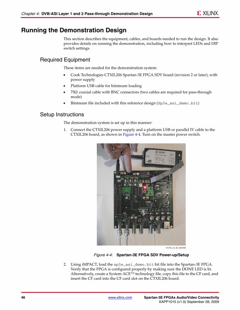
46 www.xilinx.com Spartan-3E FPGAs Audio/Video ConnectivityXAPP1015 (v1.0) September 28, 2009
Chapter 4: DVB-ASI Layer 1 and 2 Pass-through Demonstration Design
Running the Demonstration DesignThis section describes the equipment, cables, and boards needed to run the design. It also provides details on running the demonstration, including how to interpret LEDs and DIP switch settings.
Required EquipmentThese items are needed for the demonstration system:
• Cook Technologies CTXIL206 Spartan-3E FPGA SDV board (revision 2 or later), with power supply
• Platform USB cable for bitstream loading
• 75Ω coaxial cable with BNC connectors (two cables are required for pass-through mode)
• Bitstream file included with this reference design (Sp3e_asi_demo.bit)
Setup InstructionsThe demonstration system is set up in this manner:
1. Connect the CTXIL206 power supply and a platform USB or parallel IV cable to the CTXIL206 board, as shown in Figure 4-4. Turn on the master power switch.
2. Using iMPACT, load the sp3e_asi_demo.bit bit file into the Spartan-3E FPGA. Verify that the FPGA is configured properly by making sure the DONE LED is lit. Alternatively, create a System ACE™ technology file, copy this file to the CF card, and insert the CF card into the CF card slot on the CTXIL206 board.
X-Ref Target - Figure 4-4
Figure 4-4: Spartan-3E FPGA SDV Power-up/Setup
X1015_c4_04_062409

Spartan-3E FPGAs Audio/Video Connectivity www.xilinx.com 47XAPP1015 (v1.0) September 28, 2009
Design Summary
3. Connect the coaxial cables. For pass-through mode, two cables are required. One cable should connect the upstream ASI device to the VID RX1 BNC connector input of the CTXIL206 board. The other cable should connect the VID TX1 BNC output on the CTXIL206 board to the downstream ASI device.
4. Select pass-through mode by setting DIP switch two to OFF (see Figure 4-5 for DIP switch locations). Ensure that the LED next to the VID TX1 output is steady, not flashing. Press PB2 to clear all errors. When using an external stimulus stream not compatible with the board’s pattern checker, LED D is red, indicating pattern errors. In this case, the error is expected and can be ignored. The test can be assumed successful if the MPEG-2 stream(s) on the VID RX1 input are successfully transferred to the VID TX1 output and to the downstream ASI device. However, no error conditions other than LED D being red should be seen. For this mode, the Spartan-3E FPGA SDV LEDs should appear as shown in Figure 4-8.
5. If loopback mode is desired, connect a single cable from the VID TX1 output to the VID RX1 input and set DIP switch 2 to ON. This selects stimulus/loopback mode. Ensure that the LED next to the VID TX1 output is flashing. Press PB2 to clear all errors. If the demonstration is running correctly, the Spartan-3E FPGA SDV LEDs should appear as in Figure 4-7. Refer to “Design Summary” for details on individual LEDs.
Design SummaryIn summary, the receiver first looks for the ASI sync byte pattern to frame to. After this pattern is detected, the receiver monitors the disparity and code error outputs of the 8B/10B decoder to ensure that the link is still valid. Successful synchronization of the incoming data stream is indicated by the LED next to the VID RX 1 BNC connector turning green. If this LED is red, the sync byte sequence has not been detected, the decoder is reporting errors, or both. Figure 4-6 shows the VID RX1 and VID TX1 LEDs; the VID RX1 LED is red, indicating that the input has not been synchronized (i.e., framed). Monitoring of the incoming stream is continuous.
X-Ref Target - Figure 4-5
Figure 4-5: Spartan-3E FPGA SDV DIP Switch Settings
X1015_c4_05_052109

48 www.xilinx.com Spartan-3E FPGAs Audio/Video ConnectivityXAPP1015 (v1.0) September 28, 2009
Chapter 4: DVB-ASI Layer 1 and 2 Pass-through Demonstration Design
The reference design has two primary modes of operation. In the first mode, called pass-through, the CTXIL206 Spartan-3E FPGA SDV board is inserted between two other ASI devices, allowing for customer demonstrations. In this mode, the ASI receiver recovers and decodes data, then passes it directly to the transmitter for transmission, forming a pass-through. If data passes through the receiver and transmitter error-free, it can be assumed that both the receiver and transmitter work correctly. Correct operation of the transmitter and receiver can be verified by LED outputs.
In the second mode, transmitter and receiver are disconnected. Instead of transmitting data recovered by the receiver, the transmitter transmits data generated by an internal stimulus generator. The stimulus generator (Stream Source module) produces synthetic MPEG-2 packets compatible with the internal pattern checker (Stream Checker). This MPEG-2 test stream is also compatible with the pattern checker in Virtex®-5 FPGA DVB-ASI reference designs. Correct operation of this mode can be verified by using test equipment to display the synthetic MPEG-2 packets, or by looping the CTXIL206 transmitter output back the to the CTXIL206 receiver and observing the LEDs.
LEDs B and C are used by the decoder to indicate disparity and code errors, respectively. When these LEDs are green, no errors have been detected. These LEDs are persistent. If one error is detected, the LED turns red and remains red until cleared. LEDs are cleared by pressing the PB2 button.
LED D indicates errors in the pattern checker. As detailed in Chapter 2, “DVB-ASI Layer 1 and 2 Receiver,” the pattern checker removes incoming sync bytes from the data stream, waits for an MPEG-2 header byte, and then checks the remaining 188 bytes of the packet against the expected pattern. If an error is detected, LED D turns red. LED D is also used to verify that the receiver is receiving packets. A watchdog timer resets each time an MPEG-2 header byte is detected. If a header byte is not detected within two MPEG-2 packets, LED D turns red. As with the other LEDs, pressing PB2 clears the LED. Figure 4-7 shows LEDs A–D with no errors. Figure 4-8 shows the same LEDs with pattern check errors detected. Pushbuttons PB0–PB3 can also be seen in both figures.
X-Ref Target - Figure 4-6
Figure 4-6: ASI RX Not Framed
X1015_C4_06_052109

Spartan-3E FPGAs Audio/Video Connectivity www.xilinx.com 49XAPP1015 (v1.0) September 28, 2009
Design Summary
The LED next to the VID TX1 connector indicates the mode of operation. When the design is running in pass-through mode, the VID TX1 LED is steady. When the design is operating in loopback mode, the LED blinks at about 1 Hz.
LED A indicates the DCM lock condition. If this LED is green, the DCMs are locked and functioning properly. If red, the DCMs are not locked. The DCMs can be reset by pressing PB1. After resetting the DCMs, errors appear on the other LEDs, but these can be cleared by pressing PB2. LED A is not persistent.
X-Ref Target - Figure 4-7
Figure 4-7: ASI RX LEDs (No Errors)
X-Ref Target - Figure 4-8
Figure 4-8: ASI RX LEDs (Pattern Errors)
X1015_c4_07_052109
X1015_c4_08_052109

50 www.xilinx.com Spartan-3E FPGAs Audio/Video ConnectivityXAPP1015 (v1.0) September 28, 2009
Chapter 4: DVB-ASI Layer 1 and 2 Pass-through Demonstration Design
PB4 is used to issue a manual reframe request. Pressing this button forces the design to go through the link synchronization process again. This button also reinitializes the 8B/10B decoder, which can result in disparity errors, code errors, or both. Pressing PB2 clears these errors.
ConclusionThis chapter describes a DVB-ASI pass-through demonstration design for Spartan-3E devices. The reference design provides a complete pass-through function, allowing for testing in a commercial video environment.

Reference Designs for the Broadcast Industry: Volume 3 [optional]
XAPP1015 (v1.0) September 28, 2009 [optional]
Section II:SD-SDI Using Spartan-3E FPGA SelectIO LVDSAudio/Video Connectivity Solutions for Spartan-3E FPGAs

Spartan-3E FPGAs Audio/Video Connectivity www.xilinx.com XAPP1015 (v1.0) September 28, 2009
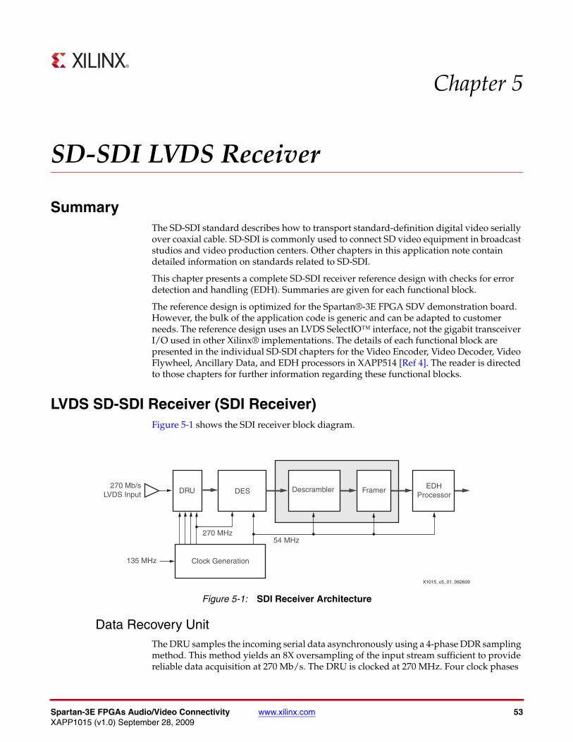
Spartan-3E FPGAs Audio/Video Connectivity www.xilinx.com 53XAPP1015 (v1.0) September 28, 2009
Chapter 5
SD-SDI LVDS Receiver
SummaryThe SD-SDI standard describes how to transport standard-definition digital video serially over coaxial cable. SD-SDI is commonly used to connect SD video equipment in broadcast studios and video production centers. Other chapters in this application note contain detailed information on standards related to SD-SDI.
This chapter presents a complete SD-SDI receiver reference design with checks for error detection and handling (EDH). Summaries are given for each functional block.
The reference design is optimized for the Spartan®-3E FPGA SDV demonstration board. However, the bulk of the application code is generic and can be adapted to customer needs. The reference design uses an LVDS SelectIO™ interface, not the gigabit transceiver I/O used in other Xilinx® implementations. The details of each functional block are presented in the individual SD-SDI chapters for the Video Encoder, Video Decoder, Video Flywheel, Ancillary Data, and EDH processors in XAPP514 [Ref 4]. The reader is directed to those chapters for further information regarding these functional blocks.
LVDS SD-SDI Receiver (SDI Receiver)Figure 5-1 shows the SDI receiver block diagram.
Data Recovery UnitThe DRU samples the incoming serial data asynchronously using a 4-phase DDR sampling method. This method yields an 8X oversampling of the input stream sufficient to provide reliable data acquisition at 270 Mb/s. The DRU is clocked at 270 MHz. Four clock phases
X-Ref Target - Figure 5-1
Figure 5-1: SDI Receiver Architecture
X1015_c5_01_062609
Framer EDHProcessor
Clock Generation
270 Mb/sLVDS Input DRU DES Descrambler
135 MHz
54 MHz270 MHz
54 www.xilinx.com Spartan-3E FPGAs Audio/Video ConnectivityXAPP1015 (v1.0) September 28, 2009
Chapter 5: SD-SDI LVDS Receiver
(0°, 45°, 90°, and 135°), each clocking two sampling flip-flops (positive and negative edge triggered), provide a total of two sample points per clock phase, 180° apart. This gives a total of eight sample points per bit interval.
The output of each sample pair is double-registered to prevent metastability. A state machine examines the resulting samples and determines edge positions as well as which registers contain valid data samples. The correctly chosen samples are then output from the DRU at a rate of zero, one, or two bits per clock, depending on the sample point. A 2-bit data valid output indicates when the data is valid as well as how many bits should be shifted for deserialization, as discussed in “Deserializer,” page 55.
Implementation of the high-speed 270 MHz circuitry in a Spartan device requires the use of advanced design techniques and Xilinx tool capabilities. To meet timing consistently, this portion of the SDI receiver utilizes relationally placed macros (RPMs) and directed routing. RPMs provide a method of preserving the relative placement of components to allow the macro to be relocated (manually or automatically), while preserving design performance. Directed routing is an advanced tool feature that preserves the routing of individual nets, regardless of implementation runs or parameters. Directed routing allows the high-performance block to be relocated to other areas on the device as needed while preserving performance.
DRU Advanced Implementation
This section contains advanced information and assumes familiarity with RPMs, directed routing, and the routing details of the target FPGA architecture. The source files (DRU.v/vhd) should be referred to when studying this section.
As discussed in “Data Recovery Unit,” the DRU uses eight sample flip-flops to provide the 8X oversampling of the input. For the 8X oversampling and data recovery to work correctly, the sample points need to be equally spaced within the sample window. To ensure this, the 8-sample flip-flops utilize relative placement constraints to lock the flip-flop placement relative to the I/O and to each other. This enables a low-skew route of the input net to each sample flip-flop. Figure 5-2, page 55 shows the placement of these sample flip-flops in a Spartan-3E FPGA 3S1600E. This relative placement allows the designer to manage routing delays to each sample flip-flop with minimal skew. The eight primary sampling flip-flops are denoted QR, QR0, QR1, and QR2 for the rising-edge samples, and QF, QF0, QF1, and QF2 for the falling-edge samples. Figure 5-2, page 55 shows the slices highlighted for each flip-flop location. In some cases, additional flip-flops are included in the RPM within these slices for metastability.
In addition to the relative placement, directed routing constraints are applied to the routing from the LVDS input pads to the eight sampling flip-flops. This preserves performance between iterative implementations of the reference design. Directed routing is a way to preserve routing, down to the exact wire, regardless of the implementation settings, and ensures that the sampling flip-flops always work correctly. The reference design presented contains a total of 13 directed routes. Directed routing strings are first extracted using FPGA Editor. Then, these strings are used in the VHDL code. This ensures that each time the design is synthesized, the special routing directives are embedded into the resulting synthesis netlist and are preserved all the way through to the bitstream.
During the routing phase of the implementation, PAR provides the following feedback in the route report indicating whether or not the directed routes were successful:
"Starting Router
# of EXACT MODE DIRECTED ROUTING found:13, SUCCESS:13, FAILED:0"

Spartan-3E FPGAs Audio/Video Connectivity www.xilinx.com 55XAPP1015 (v1.0) September 28, 2009
LVDS SD-SDI Receiver (SDI Receiver)
If the status above indicates any failed routes, a problem was encountered during the routing phase, and it should not be assumed that the circuit is functioning properly.
In Figure 5-2, the asi_datain net is highlighted to show the critical routes that require directed routing constraints. The directed routing attribute for this net is shown in the top-level design file and must be preserved to maintain the low-skew route. Additional directed routing strings, along with the RLOC constraints for the RPM, are found in the source file DRU.vhd. The RLOC_ORIGIN constraint to locate the RPM on the FPGA grid is set in the UCF file included with the reference design.
DeserializerIn high-speed serial communications systems, it is necessary for practical reasons to convert the high-frequency bit rate of the incoming serial data to a more manageable frequency. The deserializer provides this function. In essence, the deserializer is a serial-to-parallel converter. In its simplest form, it converts the single-bit serial input stream into a multiple-bit parallel word and a parallel clock rate inversely proportional to the number of bits in the parallel word. This conversion from the serial rate to the parallel rate is generally expressed as a ratio. For example, a 1:8 ratio produces 8-bit words at 1/8th the frequency of the serial bit rate. If the serial input frequency is 320 Mb/s, the deserializer outputs 8-bit words at 40 MHz.
The SD-SDI receiver deserializer provides a 1:10 ratio. Samples are collected from the DRU at a rate of zero, one, or two bits per serial clock until a 10-bit word is collected. The 10-bit word is output along with a data valid output indicating a valid new word. This signal toggles, on average, at the word clock rate of 27 MHz and is synchronous to the 0° phase 270 MHz clock. As discussed in “Clock Generation,” page 32, a 54 MHz clock is provided
X-Ref Target - Figure 5-2
Figure 5-2: DRU Sample Flip-Flops and Input
X1015_c5_02_052009

56 www.xilinx.com Spartan-3E FPGAs Audio/Video ConnectivityXAPP1015 (v1.0) September 28, 2009
Chapter 5: SD-SDI LVDS Receiver
for the parallel datapath of the reference design. The deserializer clock enable is also synchronous to this clock, and all circuitry downstream from the deserializer runs at the 54 MHz rate.
On average, the deserializer generates 10-bit words at a 27 MHz rate. The data valid output therefore toggles, on average, every cycle of the 54 MHz clock. On occasion, due to the asynchronous sampling of the input stream, the deserializer can produce two 10-bit words in a single 54 MHz period.
Video DecoderPrior to processing, video data must be encoded according to the SD-SDI standard. This ensures that the data stream is polarity free and the receiver can recover the stream clock and extract data. The data stream is encoded such that sufficient level transitions are present to allow a PLL or other circuit to lock onto the signal and extract a clock, if needed.
After oversampling and recovering data from the encoded serial stream, the receiver must recover the original raw video data and timing signals. The descrambler provides this function. The descrambler decodes the original data by reversing the original encoder polynomial scrambling.
After the data has been descrambled, it must be framed to align on the correct 10-bit or 8-bit word boundaries. The framer provides this function. To enable framing, a unique, repeating pattern called a timing reference symbol (TRS) is provided that is guaranteed not to occur in the data itself. The framer looks for this pattern and rotates the 10-bit parallel word from the DRU to align the 10-bit words correctly.
EDH ProcessorThe EDH processor provides an error-detection mechanism suitable for a basic SDI receiver. The EDH protocol is an optional but commonly used addition to the SD-SDI standard. It allows an SD-SDI receiver to verify that each field of video is received correctly. The EDH processor does not provide error correction.
In addition to error detection and handling, the EDH processor also provides TRS detection and decoding of the field, vertical, and horizontal timing signals. This feature is useful for genlock applications, where an external device generates a new pixel clock based on decoded timing signals. The EDH processor also detects and identifies the incoming video standard (six SD standards are supported). It can also identify when the current video position is in the synchronous switching interval.
The EDH processor can be implemented using only gates. However, the complexity of the EDH protocol requires that such an implementation be an inefficient use of FPGA resources. A more efficient approach uses a simple microprocessor implemented in the FPGA fabric. The Xilinx PicoBlaze™ processor provides an efficient way to reduce design size while providing the needed functionality.
ClockingThe receiver requires a minimum of five clocks: four 270 MHz clocks at four different phases (0°, 45°, 90°, and 135°) and one 54 MHz clock. The 270 MHz clocks are used by the 8X oversampler to create the necessary sample points, as described in “Data Recovery Unit,” page 53. The 54 MHz clock is used for the remaining receiver blocks, including the deserializer and all downstream logic such as the decoder and framer.

Spartan-3E FPGAs Audio/Video Connectivity www.xilinx.com 57XAPP1015 (v1.0) September 28, 2009
Module I/O
The EDH processor also requires a clock in the 27 MHz to 54 MHz range for the PicoBlaze™ processor. This is because the PicoBlaze processor does not support a clock enable. Therefore, the 270 MHz clock and clock enable cannot be used. The PicoBlaze processor can be, but is not required to be, synchronous to the 270 MHz clock. Complete synchronization is provided where these two clock domains are crossed. The PicoBlaze processor clock speed is somewhat dependent on the specific SD video standard used. If only 4:2:2 SD video is being processed, 27 MHz is sufficient. If 4:4:4:4 SD video (the worst case) is being processed, a clock frequency of 54 MHz should be used.
Module I/OTable 5-1 describes the input and output ports of the RX module.
Table 5-1: SDI Receiver Ports (sdi_rx_softedh_sp3e.v/.vhd)
Name I/O Width Description
clk_270_4phase I 4 This input provides four 270 MHz clocks, each with a different phase (0°, 90°, 135°, and 270°).
clk_54 I 1 This is a 54 MHz parallel path clock.
Cpuclk I 1 This is the clock for the PicoBlaze processor in the EDH processor. It ranges in frequency from 27 MHz to 54 MHz and does not need to be synchronous to vidclk.
Rst I 1 This is the asynchronous reset for all logic elements except the PicoBlaze processor.
rst_cpu I 1 This is the synchronous reset for the PicoBlaze processor only.
sdi_datain I 1 This is a 270 Mb/s serial SDI data input.
err_flg_en I 16 This is an error flag enable for the EDH processor that enables particular error flags.
en_sync_switch I 1 This is an enable for fast synchronizing to the end-of-active video (EAV) during the synchronous switching interval.
hd_sd O 1 This output indicates whether the standard is HD or SD. For this reference design, only SD is supported.
Std O 3 This output indicates the currently detected standard. It is only valid when std_locked is asserted.
std_locked O 1 This output is asserted when the EDH processor standard detector is locked to the incoming standard.
vid_out O 10 This outputs decoded and delayed output video. Video out is delayed to match all timing signal outputs.
sync_switch O 1 This output indicates that the video stream is currently in the synchronous switching interval.
F O 1 This output is the field bit timing signal. It indicates which video field is currently active.
V O 1 This is the vertical blanking interval timing signal. It is asserted when the vertical blanking interval is active.

58 www.xilinx.com Spartan-3E FPGAs Audio/Video ConnectivityXAPP1015 (v1.0) September 28, 2009
Chapter 5: SD-SDI LVDS Receiver
Reference DesignThe receiver reference design is verified in hardware on the Cook Technologies CTXIL206 SDV board and can be instantiated using the sdi_rx_softedh_sp3e.v/.vhd file. The reference design files can be downloaded at: https://secure.xilinx.com/webreg/clickthrough.do?cid=133622. Open the ZIP archive and extract the file xapp1015_sec2_ASI_LVDS.zip.
ConclusionThis chapter presents a complete SD-SDI receiver reference design implemented in a Spartan-3E FPGA using SelectIO technology. EDH processing using an efficient PicoBlaze processor is also provided and demonstrates a cost-effective solution for SD-SDI.
h O 1 This is the horizontal blanking interval timing signal. It is asserted when the horizontal blanking interval is active.
Trs O 1 This output is asserted when the current video output is the TRS.
Nsp O 1 This output is asserted when the framer detects a framing position different from the original starting framing position.
h_pos O 12 This output indicates the current horizontal (line) position of the video.
v_pos O 10 This output indicates the current vertical (line) position of the video.
Packet_flags O 4 This output provides four EDH output flags. It is enabled by err_flg_en.
edh_ap_err O 1 This output is asserted when an EDH error is detected in the active-picture portion of the video.
edh_ff_err O 1 This output is asserted when a full-field EDH error has occurred.
ap_flags O 5 This output provides five active-picture flags.
ff_flags O 5 This output provides five full-field flags.
anc_flags O 5 This output provides five ancillary data packet flags.
err_detected O 1 This output indicates detection of an EDH error, as defined by the enabled err flags.
Table 5-1: SDI Receiver Ports (sdi_rx_softedh_sp3e.v/.vhd) (Cont’d)
Name I/O Width Description

Spartan-3E FPGAs Audio/Video Connectivity www.xilinx.com 59XAPP1015 (v1.0) September 28, 2009
Chapter 6
SD-SDI LVDS Transmitter
SummaryThe SD-SDI standard describes how to transport standard-definition digital video serially over coaxial cable. SD-SDI is commonly used to connect SD video equipment in broadcast studios and video production centers. Other chapters in this application note contain detailed information on standards related to SD-SDI.
This chapter presents a complete SD-SDI transmitter reference design with EDH generation, ancillary data multiplexing, and internal video pattern generation. Summaries are given for each functional block.
The reference design is optimized for the Spartan®-3E FPGA SDV demonstration board. However, the bulk of the application code is generic and can be adapted to customer needs. The reference design uses an LVDS SelectIO™ interface, not the gigabit transceiver interface used in other Xilinx® implementations. The details of each functional block are presented in the individual SD-SDI chapters for the Video Encoder, Video Decoder, Video Flywheel, Ancillary Data, and EDH processors in XAPP514 [Ref 4]. The reader is directed to those chapters for further information regarding these functional blocks.
SD-SDI TransmitterFigure 6-1 shows the SDI transmitter block diagram. The transmitter includes a more full-featured video processor and EDH processor than that used in the receiver. This is to provide additional capability and to show how to apply additional modules that are part of the overall suite of Xilinx video connectivity reference designs.

60 www.xilinx.com Spartan-3E FPGAs Audio/Video ConnectivityXAPP1015 (v1.0) September 28, 2009
Chapter 6: SD-SDI LVDS Transmitter
The SDI transmitter includes video standard detection, an internal pattern generator, a flywheel (for noise immunity), ancillary and EDH processors that provide ancillary data multiplexing and EDH generation, an SDI video encoder (also known as a scrambler), and a 10:1, 135 MHz/270 Mb/s dual data-rate (DDR) serializer. A multiplexed video input port is provided for choosing between the internal pattern generator and another video source.
Video Pattern GeneratorVideo pattern generators are often included with modern video test equipment to provide internal diagnostics or known video test data. From this perspective, it is useful for a transmitter to have an embedded video pattern generator.
The included video pattern generator is a simple NTSC video generator that generates SMPTE EG-1 color bars or the RP178 check field. The SMPTE EG-1 color bar pattern is the preferred pattern for image generation. The RP178 check field can be used to stress the PLL and cable equalizer of attached video equipment. Detailed information on this pattern generator as well as other video pattern generators (e.g., PAL) is available in the “SDTV Video Pattern Generators” chapter of Audio/Video Connectivity Solutions for Virtex®-II Pro and Virtex-4 FPGAs [Ref 4]. The desired pattern (EG-1 or RP178) is selectable via an input to the SDI transmitter module.
Standard Detect and FlywheelEDH packets and ancillary data are often inserted into SDI streams. The location of this data is dependent on the video standard. Consequently, any video processor must first detect the video standard to properly locate and modify (if needed) ancillary data or EDH packets. Standard detection, in its simplest form, involves detecting and decoding the TRS word in the video stream. The TRS word contains timing information regarding the current field, and vertical and horizontal blanking. Video processors use this information to determine the start of a new video line, calculate how many video words are present on a line, and compare it to the known standards.
In addition to correctly detecting the standard, the video processor must also synchronize to the incoming video stream. This allows it to know the horizontal and vertical positions of the current video sample. Using this information, the processor can insert, modify, or
X-Ref Target - Figure 6-1
Figure 6-1: SDI TX Architecture
X1015_c6_01_052009
Clock/Clock Enable(CE) Generation
VideoIn
patt_gen_en
10
CE
135 MHz Clock
Video Processor(Standard Detectand Flywheel)
ANC/EDHProcessor
VideoEncoder
Serializer
VideoPattern
Generator

Spartan-3E FPGAs Audio/Video Connectivity www.xilinx.com 61XAPP1015 (v1.0) September 28, 2009
SD-SDI Transmitter
delete ancillary data packets and EDH check words as needed. For this reference design, a special type of video processor is used that provides not only these vital functions, but some measure of noise immunity as well. This type of processor is called a flywheel. A video flywheel, like its mechanical counterpart, can recover from noisy, or briefly interrupted video streams and provide consistent video timing data to the downstream video equipment. These features make the overall system more reliable.
The flywheel, like a standard video processor, first attempts to synchronize itself to the incoming video stream by decoding the TRS symbols. However, unlike a standard video processor, after the flywheel locks to the incoming source, it generates its own video timing signals. The flywheel also continuously monitors the incoming video timing signals and compares them to its internal timing signals. When a difference in timing occurs (due to noise or switching), the flywheel does not immediately lose lock and try to reacquire the video signal, as a standard processor would. Rather, it continues to generate correct video timing signals (analogous to momentum in a mechanical flywheel). In most cases, the noisy input video corrects itself. However, if the signal continues to be noisy or switches to a different standard, the flywheel eventually drops its lock and reacquires the input timing. An input to the transmitter is also provided that, when asserted, forces the flywheel to reacquire the input signal.
In addition to noise immunity, the video flywheel can also correct invalid TRS symbols. Because the flywheel continues to generate correct TRS symbols even when the video source is disconnected, downstream video equipment can remain synchronized, even though the visual information in the data is invalid.
The standard detection and flywheel are described in detail in the “SD-SDI Video Flywheel” chapter of Audio/Video Connectivity Solutions for Virtex-II Pro and Virtex-4 FPGAs [Ref 4].
Ancillary Data/EDH ProcessorAncillary and EDH processing can involve several different steps. In general, ancillary data can be multiplexed (inserted) into the video stream, demultiplexed (extracted) from the video stream, or both. EDH processing can involve checking and generation. The SDI TX implementation in this reference design implements ancillary data multiplexing and EDH generation.
Ancillary data multiplexing can be used to place a wide variety of “non-video” information into the encoded video stream. EDH packets are, in fact, a form of ancillary data with special identifiers that denote them as EDH packets.
The included EDH processor provides an input (receive_mode) to disable the EDH processor receiver functions. This mode is useful in transmitter-only applications because errors would be flagged on the incoming video if no EDH packet is present. For example, when using the internal pattern generators as the video source, the EDH packet is not present. Therefore, the receive_mode input should be set to disable the receiver functions to avoid false errors in the EDH packet. If this mode is enabled, the EDH processor performs cyclic redundancy checks (CRCs) on the incoming EDH packet. See Table 6-1, page 62 for more information about the receive_mode input.
The ancillary data multiplexer in the included EDH processor allows insertion of any type of ancillary data into the video stream. The multiplexer takes several inputs, properly formats the user defined data into a new ancillary (ANC) packet, and inserts the new ANC packet into available ANC space.
The EDH generator inserts new EDH packets into the video stream. It does this by generating a new packet (if one is not already present) or by modifying the existing EDH

62 www.xilinx.com Spartan-3E FPGAs Audio/Video ConnectivityXAPP1015 (v1.0) September 28, 2009
Chapter 6: SD-SDI LVDS Transmitter
packet. New CRC values are calculated and any internal error flags are set. Several inputs are provided for the purpose of inserting internal errors. These inputs are documented in “Module I/O,” page 62.
Video EncoderPrior to transmission, raw video data must be encoded to the SDI standard. This encoding process ensures a polarity-free, transition-rich data stream for the SDI receiver to lock onto. The encoding process uses a simple polynomial scrambler for this purpose. Several methods exist to implement the encoder, but the reference design of this chapter uses a simple parallel architecture. The details of the encoder can be found in the “SD-SDI Video Encoder” chapter of Audio/Video Connectivity Solutions for Virtex-II Pro and Virtex-4 FPGAs [Ref 4].
SerializerThe final logic block in the transmitter is the serializer. In this reference design, the serializer provides a 10:1 serialization ratio. To make the serializer more portable to other Xilinx FPGAs, it uses a DDR, or half bit-rate clock, instead of a full bit-rate clock. Current Xilinx FPGAs include DDR registers in the I/O blocks that make it easier to implement DDR functionality. The serializer shifts two bits per clock cycle into the output DDR register, which then shifts the final output data. Thus, serialization has two stages. The first stage slices the 10-bit input word into five sequential 2-bit slices. In the second stage, the DDR register provides the final 2:1 serialization.
Clocking The transmitter requires only a single clock and clock enable to function. The serializer uses a half bit-rate clock. Therefore, the transmitter half bit-rate clock is 135 MHz. This clock can be supplied to all transmitter functions if a suitable word rate clock enable is also generated. In this reference design, a simple clock enable generator provides clock enable pulses at the rate of 1/5th of the 135 MHz clock. This is equivalent to a 27 MHz video rate. Only a small portion of the serializer uses the 135 MHz clock, which simplifies timing closure.
Module I/OTable 6-1 describes the input and output ports of the TX module.
Table 6-1: SDI TX Ports (sdi_tx.v/.vhd)
Port I/O Width Description
clk I 1 This is the half bit-rate clock, or word rate clock. If using a word rate clock, it must be synchronous with the serclk_0 input.
ce I 1 This is the clock enable input for the clk domain. It should be at 1/5th of the serclk rate if clk is the same as serclk_0.
rst I 1 This is the asynchronous reset input that resets all logic.
vid_in I 10 This is the unencoded (raw) video input.
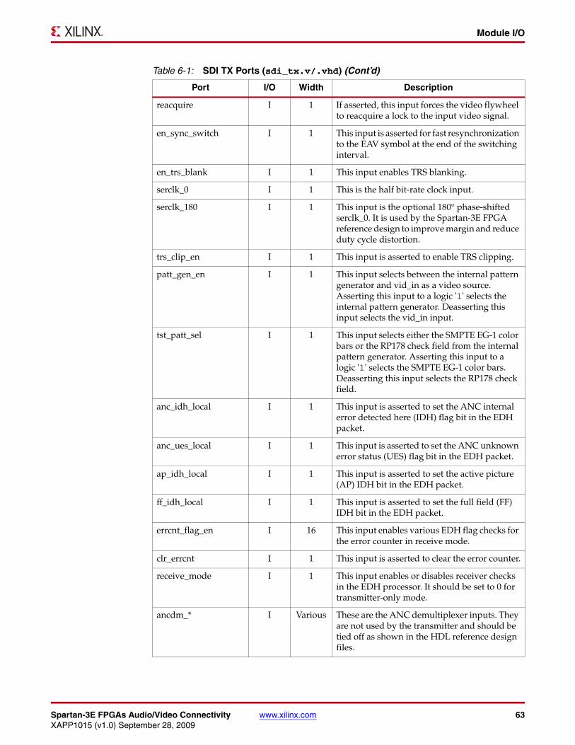
Spartan-3E FPGAs Audio/Video Connectivity www.xilinx.com 63XAPP1015 (v1.0) September 28, 2009
Module I/O
reacquire I 1 If asserted, this input forces the video flywheel to reacquire a lock to the input video signal.
en_sync_switch I 1 This input is asserted for fast resynchronization to the EAV symbol at the end of the switching interval.
en_trs_blank I 1 This input enables TRS blanking.
serclk_0 I 1 This is the half bit-rate clock input.
serclk_180 I 1 This input is the optional 180° phase-shifted serclk_0. It is used by the Spartan-3E FPGA reference design to improve margin and reduce duty cycle distortion.
trs_clip_en I 1 This input is asserted to enable TRS clipping.
patt_gen_en I 1 This input selects between the internal pattern generator and vid_in as a video source. Asserting this input to a logic '1' selects the internal pattern generator. Deasserting this input selects the vid_in input.
tst_patt_sel I 1 This input selects either the SMPTE EG-1 color bars or the RP178 check field from the internal pattern generator. Asserting this input to a logic '1' selects the SMPTE EG-1 color bars. Deasserting this input selects the RP178 check field.
anc_idh_local I 1 This input is asserted to set the ANC internal error detected here (IDH) flag bit in the EDH packet.
anc_ues_local I 1 This input is asserted to set the ANC unknown error status (UES) flag bit in the EDH packet.
ap_idh_local I 1 This input is asserted to set the active picture (AP) IDH bit in the EDH packet.
ff_idh_local I 1 This input is asserted to set the full field (FF) IDH bit in the EDH packet.
errcnt_flag_en I 16 This input enables various EDH flag checks for the error counter in receive mode.
clr_errcnt I 1 This input is asserted to clear the error counter.
receive_mode I 1 This input enables or disables receiver checks in the EDH processor. It should be set to 0 for transmitter-only mode.
ancdm_* I Various These are the ANC demultiplexer inputs. They are not used by the transmitter and should be tied off as shown in the HDL reference design files.
Table 6-1: SDI TX Ports (sdi_tx.v/.vhd) (Cont’d)
Port I/O Width Description

64 www.xilinx.com Spartan-3E FPGAs Audio/Video ConnectivityXAPP1015 (v1.0) September 28, 2009
Chapter 6: SD-SDI LVDS Transmitter
ancm_hanc_pkt I 1 This input is asserted to insert ANC data into the horizontal ANC space.
ancm_vanc_pkt I 1 This input is asserted to insert ANC data into the vertical ANC space.
ancm_pkt_rdy_in I 1 This input is asserted to indicate that an ANC packet is ready for insertion.
ancm_cal_udw_par I 1 This input is asserted to enable automatic user data word (UDW) parity calculation.
ancm_din I 10 This is the ANC data input.
ancm_ld_did I 1 This input is asserted to load a data identity (DID) value into the ANC buffer space for packet assembly.
ancm_ld_dbn I 1 This input is asserted to load a data block number (DBN) value into the ANC buffer space for packet assembly.
ancm_ld_dc I 1 This input is asserted to load a data count (DC) value into the ANC buffer space for packet assembly.
ancm_ld_udw I 1 This input is asserted to load a UDW into the ANC buffer. It is asserted once for each UDW up to the DC total.
ancm_udw_wr_adr I 8 This is the UDW write address.
std O 3 This is the decoded video standard. It is only valid when std_locked is asserted.
std_locked O 1 This output is asserted to indicate that the flywheel decoder is locked to the video input.
trs O 1 This output is asserted when the current video word is the TRS.
field O 1 This output indicates a current active field.
v_blank O 1 This output is asserted during the vertical blanking interval.
h_blank O 1 This output is asserted during the horizontal blanking interval.
horz_count O 12 This output specifies the current horizontal (line) position.
vert_count O 10 This output specifies the current vertical (line) position.
sync_switch O 1 This output is asserted to indicate that video is in the synchronous switching interval.
locked O 1 This output indicates that the EDH processor is locked to the video.
Table 6-1: SDI TX Ports (sdi_tx.v/.vhd) (Cont’d)
Port I/O Width Description

Spartan-3E FPGAs Audio/Video Connectivity www.xilinx.com 65XAPP1015 (v1.0) September 28, 2009
Reference Design
Reference DesignThe individual transmitter can be instantiated using the sdi_tx.v/.vhd modules. The reference design is verified in hardware on the Cook Technologies CTXIL206 SDV board and can be downloaded at: https://secure.xilinx.com/webreg/clickthrough.do?cid=133622. Open the ZIP archive and extract the file xapp1015_sec2_ASI_LVDS.zip.
ConclusionThis chapter presents a complete SD-SDI transmitter reference design implemented in a Spartan-3E FPGA using SelectIO technology. The transmitter also provides a flywheel for noise immunity and ancillary data multiplexing to enable insertion of user-defined ancillary data. This reference design is a port of the work originally presented in Audio/Video Connectivity Solutions for Virtex-II Pro and Virtex-4 FPGAs [Ref 4].
eav_next O 1 This output marks the start of the EAV.
sav_next O 1 This output marks the start of the SAV.
xyz_word O 1 This output marks the XYZ word in the video input.
anc_next O 1 This output marks the ANC space.
edh_next O 1 This output marks the EDH space.
EDH Flag Outputs O Various This output is not used in the TX design.
ANC Demux Outputs O Various These ancillary demultiplexer outputs are not used in the transmitter design.
ancm_pkt_in_empty O 1 This output is asserted by the EDH processor to indicate that it is ready to receive ANC packet data on the ANC multiplexer inputs.
adi_txout O 1 This port outputs serialized, 270 Mb/s encoded video data.
Table 6-1: SDI TX Ports (sdi_tx.v/.vhd) (Cont’d)
Port I/O Width Description

66 www.xilinx.com Spartan-3E FPGAs Audio/Video ConnectivityXAPP1015 (v1.0) September 28, 2009
Chapter 6: SD-SDI LVDS Transmitter
Spartan-3E FPGAs Audio/Video Connectivity www.xilinx.com 67XAPP1015 (v1.0) September 28, 2009
Chapter 7
SD-SDI Receiver/Transmitter Demonstration Design
SummaryThe SD-SDI standard describes how to transport standard-definition digital video serially over coaxial cable. SD-SDI is commonly used to connect SD video equipment in broadcast studios and video production centers.
This chapter presents a complete SD-SDI receiver reference design with checks for EDH. It also presents a complete SD-SDI transmitter reference design with EDH generation, ancillary data multiplexing, and internal video pattern generation. Both receiver and transmitter are integrated into a single top-level design. The individual receiver and transmitter functions are discussed in Chapter 5, “SD-SDI LVDS Receiver” and Chapter 6, “SD-SDI LVDS Transmitter,” respectively. Summaries for each functional block are given in this chapter.
The reference design is optimized for the Spartan®-3E FPGA SDV demonstration board. However, the bulk of the application code is generic and can be adapted to customer needs. The reference design uses an LVDS SelectIO™ interface, not the gigabit transceiver interface used in other Xilinx® implementations.
Reference DesignIn addition to the SDI receiver and transmitter modules described, additional modules are provided as part of the reference design for the purpose of design robustness and demonstration. These additional modules are instantiated in the top level of the reference design. Individual receivers and transmitters can be instantiated by using the sdi_rx_softedh_sp3e.v/.vhd and sdi_tx.v/.vhd modules, respectively.
Special reset blocks are included to ensure that logic is reset properly upon startup after the clocks have become stable. In addition, a module called ancdata_gen.v/.vhd is included to demonstrate the ancillary data multiplexing feature of the transmitter. This module interfaces to the SDI transmitter and inserts pre-defined user data words into the video stream. These user data words can be seen using standard video test equipment such as the Tektronix WFM700.
The reference design files can be downloaded at: https://secure.xilinx.com/webreg/clickthrough.do?cid=133622. Open the ZIP archive and extract the file xapp1015_sec2_ASI_LVDS.zip.
The reference design checklist for this section of the application note is shown in Table 7-1.

68 www.xilinx.com Spartan-3E FPGAs Audio/Video ConnectivityXAPP1015 (v1.0) September 28, 2009
Chapter 7: SD-SDI Receiver/Transmitter Demonstration Design
Spartan-3E FPGA SDI Demonstration BoardThe Spartan-3E FPGA SDI demonstration board provides a complete demonstration of basic SDI receiver and transmitter functionality using standard video test equipment and a Spartan-3E FPGA. The demonstration consists of a complete SDI receiver with an 8X oversampler, DRU, SDI framer, decoder, and a simple PicoBlaze™ processor for EDH checking. A ChipScope™ Pro analyzer is also embedded in the reference design to allow viewing of data and error conditions. A complete SDI transmitter with SMPTE pattern generation, EDH generation, and ANC multiplexing is also provided. The transmitter and receiver are independent functional blocks that have been integrated into a single top-level design. As such, each has its own demonstration section.
Spartan-3E FPGA SDI Receiver DemonstrationThis section describes the SDI receiver demonstration design for the Spartan-3E FPGA.
Table 7-1: Section II Reference Design Checklist
Parameter Description
General
Developer Name Jeff Hutchings
Target Devices (Stepping Level, ES, Production, Speed Grades) Spartan-3E FPGAs
Source Code Provided Yes
Source Code Format VHDL, Verilog
Design Uses Code/IP from Existing Application Note, Reference Designs, Third Party, or CORE Generator™ Software
No
Simulation
Functional Simulation Performed No
Timing Simulation Performed No
Testbench Used for Functional and Timing Simulations No
Testbench Format N/A
Simulator Software/Version Used N/A
SPICE/IBIS Simulations N/A
Implementation
Synthesis Software Tools/Version Used XST 8.2i
Implementation Software Tools/Versions Used ISE® tools, version 8.2i
Static Timing Analysis Performed Yes
Hardware Verification
Hardware Verified Yes
Hardware Platform Used for Verification CTXIL206 board

Spartan-3E FPGAs Audio/Video Connectivity www.xilinx.com 69XAPP1015 (v1.0) September 28, 2009
Spartan-3E FPGA SDI Demonstration Board
Required Equipment
These items are needed for the demonstration system:
• Xilinx CTXIL206 Spartan-3E FPGA SDV board with power supply
• Platform USB cable for bitstream loading
• 75Ω coaxial cable with BNC connectors
• Bitstream files included in the original distribution:
♦ Sp3e_sdi_demo.bit
♦ Sp3e_sdi_rx.cpj
• SDI video source
• ChipScope Pro analyzer for monitoring the EDH checker and SDI data
Receiver Demonstration Setup
The RX demonstration system is set up in this manner:
1. Connect the CTXIL206 board power supply.
2. Connect a platform USB cable to the CTXIL206 board as shown in Figure 7-1.
3. Run the ChipScope Pro analyzer, open the JTAG cable, and configure the device using the sp3e_sdi_demo.bit file.
4. Load the included ChipScope project file: sp3e_sdi_rx.cpj.
X-Ref Target - Figure 7-1
Figure 7-1: RX Demonstration Setup
X1015_c7_01_062509

70 www.xilinx.com Spartan-3E FPGAs Audio/Video ConnectivityXAPP1015 (v1.0) September 28, 2009
Chapter 7: SD-SDI Receiver/Transmitter Demonstration Design
5. Connect one end of the 75Ω coaxial cable to a valid SDI video source and the other end to the VID RX1 input. The VID TX1 output can be used as an SDI source if no other sources are available.
If the reference design is functioning correctly, LED A and the LED next to the VID RX3 input are green. If LED A is red, the DCMs are not locked. If the LED next to the VID RX3 input is red, a valid SDI input source has not been detected.
Note: LED H is RED and latched in the presence of EDH errors. Press PB3 to clear the LED (shown in Figure 7-2).
6. To demonstrate the receiver, the ChipScope analyzer can be used to view data, detect errors, or both. By default, the ChipScope analyzer project triggers on the error output of the EDH checker. Under normal circumstances, if everything is working correctly, the ILA core should never trigger. The reference design can be demonstrated further by changing the trigger to detect the TRS symbol or conditions other than an error, and then viewing the data. Figure 7-3 shows the detection of an error. Figure 7-4 shows the detection of the TRS symbol.
X-Ref Target - Figure 7-2
Figure 7-2: SDI RX LEDs
X1015_c7_02_062409

Spartan-3E FPGAs Audio/Video Connectivity www.xilinx.com 71XAPP1015 (v1.0) September 28, 2009
Spartan-3E FPGA SDI Demonstration Board
X-Ref Target - Figure 7-3
Figure 7-3: EDH Error Detection
X1015_c7_03_052009
X-Ref Target - Figure 7-4
Figure 7-4: TRS Detection and Data
X1015_c7_04_052009

72 www.xilinx.com Spartan-3E FPGAs Audio/Video ConnectivityXAPP1015 (v1.0) September 28, 2009
Chapter 7: SD-SDI Receiver/Transmitter Demonstration Design
Summary
The Spartan-3E FPGA SDI receiver demonstration board provides a system to demonstrate the basics of a complete SDI receiver implemented in a Spartan-3E FPGA. The reference design includes an 8X oversampler, DRU, deserializer, parallel framer, decoder, and EDH checker. The SDI receiver reference design of this chapter is a direct port of the reference designs in the associated chapters in XAPP514 [Ref 4].
Spartan-3E FPGA SDI Transmitter DemonstrationThis section describes the SDI transmitter demonstration design for the Spartan-3E FPGA.
Required Equipment
These items are needed for the demonstration system:
• Cook Technologies CTXIL206 Spartan-3E FPGA SDV board (revision 2 or later) with power supply
• Platform USB cable for bitstream loading
• 75Ω coaxial cable with BNC connectors
• Bitstream file included in the original distribution (Sp3e_sdi_demo.bit)
• Video test equipment (or a monitor and Miranda picoLink broadcast converter, or other method of converting SDI to an input format for a standard monitor).
Transmitter Demonstration Setup
The TX demonstration system is set up in this manner:
1. Connect the power supply and platform USB cable to the CTXIL206 board, as shown in Figure 7-5.
2. Connect one end of the 75Ω BNC coaxial cable to the VID TX 1 connector as shown in Figure 7-5. Connect the other end of the coaxial cable to the appropriate test equipment, such as the picoLink converter.

Spartan-3E FPGAs Audio/Video Connectivity www.xilinx.com 73XAPP1015 (v1.0) September 28, 2009
Spartan-3E FPGA SDI Demonstration Board
X-Ref Target - Figure 7-5
Figure 7-5: TX Demonstration Setup
X1015_c7_04_062509
Demo OptionsDIP Switches
DemoPushbuttons
SDI TX Output(VID TX 1)

74 www.xilinx.com Spartan-3E FPGAs Audio/Video ConnectivityXAPP1015 (v1.0) September 28, 2009
Chapter 7: SD-SDI Receiver/Transmitter Demonstration Design
3. Locate the DEMO OPTIONS DIP switch near the power switch (see Figure 7-5). As shown in Figure 7-6, ensure that:
a. SW1 is set to ON
b. SW2 is set to OFF
c. SW3 is set to ON
d. SW4 is set to OFF
e. SW5 through SW8 are set to ON
4. This default setup generates SMPTE color bars, ANC data multiplexing, and EDH packet generation with no ANC, AP/FF IDH, or UES errors. Apply power to the board.
5. Start iMPACT and load the bitstream file sdi_tx_demo.bit. After successful configuration, LEDs A and B should be green, and the LED next to the BNC connector for VID TX 1 should be green, as shown in Figure 7-7. If viewing on a monitor or test equipment, the video pattern should look like Figure 7-8. LED A indicates that the DCM is locked. LED B and the VID TX 1 LED indicate that the video decoder is locked to the digital video produced by the internal pattern generator. These LEDs turn red if an error occurs.
X-Ref Target - Figure 7-6
Figure 7-6: DIP Switch Settings
X-Ref Target - Figure 7-7
Figure 7-7: TX LEDs
X1015_c7_06_052009
X1015_c7_07_052109
Decoder LockedDecoder Std LockedDCM Locked

Spartan-3E FPGAs Audio/Video Connectivity www.xilinx.com 75XAPP1015 (v1.0) September 28, 2009
Spartan-3E FPGA SDI Demonstration Board
Summary
The Spartan-3E FPGA SDI TX demonstration board provides for a number of options to demonstrate SDI TX functionality. By using the default setup described in “Spartan-3E FPGA SDI Transmitter Demonstration,” page 72, the SDI transmitter produces SDI video at an output rate of 270 Mb/s. The video consists of SMPTE EG-1 color bars viewable on a monitor (additional equipment required) or standard video test equipment. The output video format is NTSC 525i, 59.94 Hz, 4:2:2 component video.
In addition to video output, the reference design automatically generates and inserts the RP 165 EDH packet to demonstrate EDH generation. Detecting and viewing the packet contents requires additional video test equipment. DIP switches, as described in “Running the Demonstration,” page 75, also allow the user to set the local IDH and UES bits in the EDH packet.
The reference design also generates and inserts ancillary data packets into the output video to demonstrate ANC multiplexing. Ancillary data can be viewed using standard video test equipment. The inserted data is fixed and cannot be changed by the user.
Running the Demonstration
This section discusses the DIP switch, pushbutton, and other settings that can affect the demonstration functionality. It also describes the ancillary data format inserted into the output video and how to set up the video test equipment to view this output.
As mentioned in “Summary,” page 72, the transmitter produces SMPTE EG-1 color data by default. When using standard video test equipment to view this color bar pattern, it is common to see Luma gamut and red, green, and blue (RGB) errors. This is because the SMPTE EG-1 pattern contains gamma values that are outside the expected range of the default settings for some equipment. This is typical on the Tektronix WFM700, for example, and these errors can be safely ignored. However, the video test equipment should not report errors with respect to the AP and FF CRC or other checks, and the YCBCR gamut should be correct.
Numerous DIP switch settings affect the reference design functionality. All are located on the DEMO OPTIONS DIP switch on the CTXIL206 board. For the SDI TX design, SW1 should always be in the ON position. This disables EDH checking in the ANC/EDH
X-Ref Target - Figure 7-8
Figure 7-8: SMPTE EG-1 Color Bars
X1015_c7_08_052009
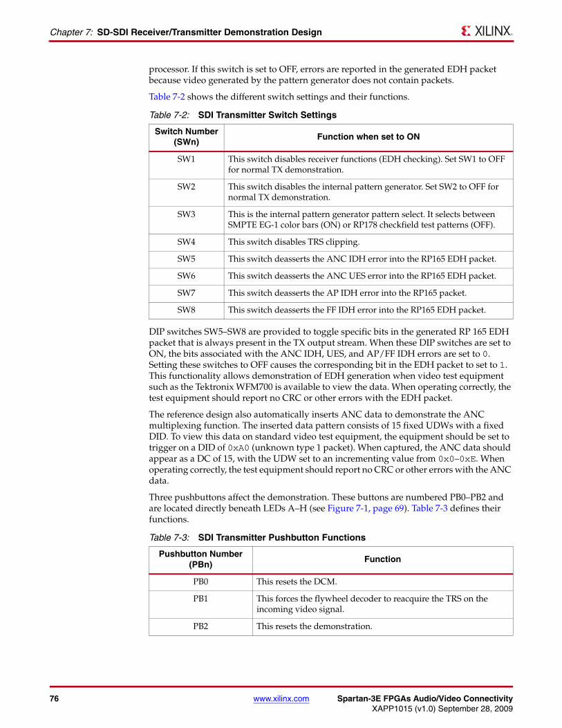
76 www.xilinx.com Spartan-3E FPGAs Audio/Video ConnectivityXAPP1015 (v1.0) September 28, 2009
Chapter 7: SD-SDI Receiver/Transmitter Demonstration Design
processor. If this switch is set to OFF, errors are reported in the generated EDH packet because video generated by the pattern generator does not contain packets.
Table 7-2 shows the different switch settings and their functions.
DIP switches SW5–SW8 are provided to toggle specific bits in the generated RP 165 EDH packet that is always present in the TX output stream. When these DIP switches are set to ON, the bits associated with the ANC IDH, UES, and AP/FF IDH errors are set to 0. Setting these switches to OFF causes the corresponding bit in the EDH packet to set to 1. This functionality allows demonstration of EDH generation when video test equipment such as the Tektronix WFM700 is available to view the data. When operating correctly, the test equipment should report no CRC or other errors with the EDH packet.
The reference design also automatically inserts ANC data to demonstrate the ANC multiplexing function. The inserted data pattern consists of 15 fixed UDWs with a fixed DID. To view this data on standard video test equipment, the equipment should be set to trigger on a DID of 0xA0 (unknown type 1 packet). When captured, the ANC data should appear as a DC of 15, with the UDW set to an incrementing value from 0x0–0xE. When operating correctly, the test equipment should report no CRC or other errors with the ANC data.
Three pushbuttons affect the demonstration. These buttons are numbered PB0–PB2 and are located directly beneath LEDs A–H (see Figure 7-1, page 69). Table 7-3 defines their functions.
Table 7-2: SDI Transmitter Switch Settings
Switch Number (SWn)
Function when set to ON
SW1 This switch disables receiver functions (EDH checking). Set SW1 to OFF for normal TX demonstration.
SW2 This switch disables the internal pattern generator. Set SW2 to OFF for normal TX demonstration.
SW3 This is the internal pattern generator pattern select. It selects between SMPTE EG-1 color bars (ON) or RP178 checkfield test patterns (OFF).
SW4 This switch disables TRS clipping.
SW5 This switch deasserts the ANC IDH error into the RP165 EDH packet.
SW6 This switch deasserts the ANC UES error into the RP165 EDH packet.
SW7 This switch deasserts the AP IDH error into the RP165 packet.
SW8 This switch deasserts the FF IDH error into the RP165 EDH packet.
Table 7-3: SDI Transmitter Pushbutton Functions
Pushbutton Number(PBn)
Function
PB0 This resets the DCM.
PB1 This forces the flywheel decoder to reacquire the TRS on the incoming video signal.
PB2 This resets the demonstration.