Embed Size (px)
Citation preview
Helsinki University of Technology Inorganic Chemistry Publication Series
Espoo 2006 No. 5
ATOMIC LAYER DEPOSITION OF HIGH-k DIELECTRICS
FROM NOVEL CYCLOPENTADIENYL-TYPE
PRECURSORS
Jaakko Niinistö Dissertation for the degree of Doctor of Science in Technology to be presented with due
permission of the Department of Chemical Technology for public examination and debate in
Auditorium TU 1 at Helsinki University of Technology (Espoo, Finland) on the 12th of May,
2006, at 12 noon.
Helsinki University of Technology
Department of Chemical Technology
Laboratory of Inorganic and Analytical Chemistry
Teknillinen korkeakoulu
Kemian tekniikan osasto
Epäorgaanisen ja analyyttisen kemian laboratorio

Distribution:
Helsinki University of Technology
Laboratory of Inorganic and Analytical Chemistry
P.O. Box 6100
FIN-02150 TKK, FINLAND
E-mail: [email protected]
© Jaakko Niinistö
ISBN 951-22-8169-4
ISSN 1458-5154
Otamedia Oy
Helsinki 2006

ABSTRACT
The atomic layer deposition (ALD) method was applied for fabricating high permittivity
(high-k) dielectrics, viz. HfO2, ZrO2 and rare earth oxides, which can be used to replace
SiO2 as gate and capacitor dielectric. The dielectrics were processed by ALD using novel
cyclopentadienyl (Cp, -C5H5) precursors together with water or ozone as the oxygen
source. ALD, which has been identified as an important thin film growth technique for
microelectronics manufacturing, relies on sequential and saturating surface reactions of
alternately applied precursors, separated by inert gas purging. The surface-controlled
nature of ALD enables the growth of thin films of high conformality and uniformity with
an accurate thickness control.
The ALD technique is introduced and ALD processes for HfO2, ZrO2 and rare earth oxide
films, as well as the applications of the high-k dielectrics in microelectronics are reviewed.
The need for developing new ALD processes for the high-k materials is emphasized.
ALD processes for HfO2 and ZrO2 were developed using Cp-type precursors. The effect of
different oxygen sources, namely water or ozone, on the film growth characteristics and
properties of the ALD-processed films was examined in detail. The oxide films were
stoichiometric, with impurity levels below even 0.1 at-% for C or H. Electrical
measurements showed promising dielectric properties such as high permittivity values and
low leakage current densities. Other properties, such as structure, interfacial layer thickness
and morphology, were also characterized. Compared to films processed by water, the
ozone-processed films on H-terminated Si showed improved dielectric properties, as well
as higher density, lower roughness and better initial growth rate. In addition, in situ gas-
phase measurements by quadrupole mass spectrometry (QMS) were performed in order to
study the ZrO2 growth mechanism.
A number of Cp-precursors were tested for the ALD of several rare earth oxide films. The
thermal stability of many of the precursors was limited, but nevertheless, ALD-type
processes were developed for Y2O3 and Er2O3 films. High reactivity of the Cp-precursors
towards water resulting in high growth rates (1.2-1.7 Å/cycle) and purity of the Y2O3 and
Er2O3 films were realized. Despite the detected partial decomposition of the (CpMe)3Gd
precursor, Gd2O3 films with high growth rate and purity as well as effective permittivity of
about 14 were deposited.

Finally, promising processes for ternary scandates, namely YScO3, GdScO3, and ErScO3,
were developed using either Cp- or β-diketonate-based processes. These as-deposited
ternary films were amorphous exhibiting high effective permittivity (14-15), low leakage
current density, and resistance towards crystallization upon annealing even up to 800°C.

PREFACE
The research reported in this thesis was carried out during the years 2001-2005 in the
Laboratory of Inorganic and Analytical Chemistry (LIAC), Helsinki University of
Technology.
I am most grateful to Dr. Matti Putkonen and Prof. Lauri Niinistö for the guidance and
advice as well as for the initiative and possibility to carry out research on this interesting
topic. My supervisor, Prof. Markku Leskelä as well as Prof. Mikko Ritala are thanked for
invaluable help and the opportunity to use the research facilities at the Laboratory of
Inorganic Chemistry, University of Helsinki.
I wish to thank all of my co-authors and co-workers from Helsinki University of
Technology, University of Helsinki, Uppsala University, and Tokyo Institute of
Technology. Especially, I would like to thank Dr. Kaupo Kukli for his assistance in the
electrical measurements, Lic. Sci. (Tech.) Jani Päiväsaari and Dr. Chuck Dezelah for good
collaboration and fruitful discussions, Mr. Pekka Hassinen for the ALD reactor
maintenance, Dr. Timo Sajavaara and Dr. Kai Arstila for the TOF-ERD analysis, Dr. Antti
Rahtu for instruction on the use of the in situ mass spectrometry system, Dr. Jun Lu, Prof.
Hisao Yamauchi, and Prof. Maarit Karppinen for providing the HR-TEM measurements,
and Prof. Pekka Hautojärvi for providing the facilities for the AFM measurements. The
other members of the inorganic chemistry staff of LIAC are thanked as well. In addition,
Dr. Chuck Dezelah is thanked for revising the language of this thesis.
Financial support from the Jenny and Antti Wihuri Foundation, Graduate School of
Inorganic Materials Chemistry, The Finnish Foundation of Technology, the Academy of
Finland and Acta Chemica Scandinavica is gratefully acknowledged.
Finally I wish to thank my family, especially my wife Sari for her continuous support.
Espoo, February 2006
Jaakko Niinistö
LIST OF PUBLICATIONS
In addition to the present review, this thesis includes the following publications (I-IX),
which are referred to in the text by their corresponding Roman numerals. In addition, some
still unpublished deposition studies of various rare earth oxide films are discussed.
I Putkonen, M., Niinistö, J., Kukli, K., Sajavaara, T., Karppinen, M., Yamauchi,
H., and Niinistö, L., ZrO2 thin films grown on silicon substrates by atomic
layer deposition with Cp2Zr(CH3)2 and water as precursors, Chem. Vap.
Deposition 9 (2003) 207-212.
II Niinistö, J., Putkonen, M., Niinistö, L., Kukli, K., Ritala, M., and Leskelä, M.,
Structural and dielectric properties of thin ZrO2 films on silicon grown by
atomic layer deposition from cyclopentadienyl precursor, J. Appl. Phys. 95
(2004) 84-91.
III Niinistö, J., Rahtu, A., Putkonen, M., Ritala, M., Leskelä, M., and Niinistö, L.,
In situ quadrupole mass spectrometry study of atomic-layer deposition of ZrO2
using Cp2Zr(CH3)2 and water, Langmuir 21 (2005) 7321-7325.
IV Niinistö, J., Putkonen, M., Niinistö, L., Stoll, S.L., Kukli, K., Sajavaara, T.,
Ritala, M., and Leskelä, M., Controlled growth of HfO2 thin films by atomic
layer deposition from cyclopentadienyl-type precursor and water, J. Mater.
Chem. 15 (2005) 2271-2275.
V Niinistö, J., Putkonen, M., Niinistö, L., Arstila, K., Sajavaara, J. Lu, T., Kukli,
K., Ritala, M., and Leskelä, M., HfO2 films grown by ALD using
cyclopentadienyl-type precursors and H2O or O3 as oxygen source, J.
Electrochem. Soc. 153 (2006) F39-F45.
VI Niinistö, J., Putkonen, M., and Niinistö, L., Processing of Y2O3 thin films by
atomic layer deposition from cyclopentadienyl-type compounds and water as
precursors, Chem. Mater. 16 (2004) 2953-2958.

VII Niinistö, J., Petrova, N., Putkonen, M., Sajavaara, T., Arstila, K., and Niinistö
L., Gadolinium oxide thin films by atomic layer deposition, J. Cryst. Growth
285 (2005) 191-200.
VIII Päiväsaari, J., Niinistö, J., Arstila, K., Kukli, K., Putkonen, M., and Niinistö,
L., High growth rate of erbium oxide thin films in atomic layer deposition from
(CpMe)3Er and water precursors, Chem. Vap. Deposition 11 (2005) 415-419.
IX Myllymäki, P., Nieminen, M., Niinistö, J., Putkonen, M., Kukli, K., and
Niinistö L., High-permittivity YScO3 thin films by atomic layer deposition
using two precursor approaches, J. Mater. Chem. 16 (2006) 563-567.

THE AUTHOR’S CONTRIBUTION
Publication I The research plan for the experimental work was made together with
Dr. Matti Putkonen. The author was responsible for carrying out a part
of the film depositions, AFM and electrical measurements. The author
had a minor role in writing the article.
Publication II The author planned the research together with Dr. Matti Putkonen and
did the experimental work except for precursor synthesis, TEM, XRR,
GI-XRD and XPS analyses. The author interpreted the results and
wrote the article.
Publication III The research plan was made together with Dr. Antti Rahtu. The author
carried out the experiments, except for the precursor synthesis,
interpreted the results together with Dr. Antti Rahtu and wrote the
article.
Publication IV The author planned the research and did the experimental work except
for a minor part of the depositions, precursor synthesis, XRR and
TOF-ERD analysis. The author interpreted the results and wrote the
article.
Publication V The author planned the research and did the experimental work except
for precursor synthesis, XRR, TEM and TOF-ERD analysis. The
author interpreted the results and wrote the article.
Publication VI The research plan for the experimental work was made together with
Dr. Matti Putkonen. The author did the experimental work except for
TOF-ERD analysis. The author interpreted the results and wrote the
article.
Publication VII The author planned the research and did the experimental work except
for TOF-ERD analysis and minor part of the depositions. The author
interpreted the results and wrote the article.

Publication VIII The author assisted in planning of the research. The author was
responsible for the AFM studies and characterizing the electrical
properties. The author had a minor role in writing the article.
Publication IX The author assisted in the planning of film growth experiments
relating to electrical measurements. The author was responsible for the
AFM studies and analyzing the electrical properties. The author had a
minor role in interpretation of the results and writing the article.

LIST OF ABBREVIATIONS AND ACRONYMS
acac acetylacetonate AES Auger Electron Spectroscopy AFM Atomic Force Microscope/Microscopy ALD Atomic Layer Deposition ALE Atomic Layer Epitaxy amd amidinate, NC(CH3)N CET Capacitance Equivalent oxide Thickness CMOS Complementary Metal Oxide Semiconductor Cp Cyclopentadienyl, C5H5 CVD Chemical Vapor Deposition dmae dimethylaminoethoxide, (CH3)2N(C2H5O) DRAM Dynamic Random Access Memory EOT Equivalent Oxide Thickness Et ethyl, -C2H5 GI Grazing Incidence HR High-Resolution IC Integrated Circuit IL Interfacial Layer iPr isopropyl,-CH(CH3)2 Me methyl, -CH3 ML Monolayer mmp 1-methoxy-2-methyl-2-propanolate MOSFET Metal Oxide Semiconductor Field Effect Transistor QMS Quadrupole Mass Spectrometry RE Rare Earth rms root mean square RTA Rapid Thermal Annealing SIMS Secondary Ion Mass Spectroscopy tBu tert-butyl, -CH(CH3)3 TEM Transmission Electron Microscopy thd 2,2,6,6-tetramethyl-3,5-heptanedione, C11H20O2 TOF-ERDA Time-Of-Flight Elastic Recoil Detection Analysis XPS X-ray Photoelectron Spectroscopy XRD X-Ray Diffraction XRF X-Ray Fluorescence XRR X-Ray Reflectivity

11
CONTENTS
ABSTRACT ............................................................................................................ 3
PREFACE................................................................................................................ 5
LIST OF PUBLICATIONS..................................................................................... 6
THE AUTHOR’S CONTRIBUTION ..................................................................... 8
LIST OF ABBREVIATIONS AND ACRONYMS .............................................. 10
CONTENTS .......................................................................................................... 11
1. INTRODUCTION............................................................................................. 13
1.1 Dielectric layers in microelectronics ........................................................... 15
1.2 Atomic layer deposition .............................................................................. 19
1.3 Precursor chemistry in ALD of oxide films ................................................ 23
1.3.1 Metal precursor types ........................................................................... 23
1.3.2 Oxygen sources .................................................................................... 26
1.4 ALD of high-k dielectrics ............................................................................ 27
1.4.1 ZrO2 ...................................................................................................... 27
1.4.2 HfO2...................................................................................................... 31
1.4.3 Rare earth oxides .................................................................................. 35
2. EXPERIMENTAL ............................................................................................ 38
2.1 Precursors and film growth ......................................................................... 38
2.2 Film characterization ................................................................................... 39
2.3 Reaction mechanism studies........................................................................ 41
3. RESULTS AND DISCUSSION........................................................................ 43
3.1 ZrO2 from cyclopentadienyl precursor ........................................................ 43
3.1.1 Reaction mechanism studies................................................................. 47
3.2 HfO2 from cyclopentadienyl precursors ...................................................... 49
3.3 Rare earth oxide thin films from cyclopentadienyl precursors.................... 52
3.3.1 Y2O3...................................................................................................... 53
3.3.2 LaOx...................................................................................................... 54
3.3.3 PrOx ...................................................................................................... 55
3.3.4 Gd2O3.................................................................................................... 56

12
3.3.5 Er2O3..................................................................................................... 57
3.3.6 Rare earth scandates ............................................................................. 58
3.3.7 Dielectric properties of the RE oxide films.......................................... 58
3.3.8 Rare earth precursor selection .............................................................. 60
4. CONCLUSIONS............................................................................................... 62
5. REFERENCES.................................................................................................. 64

13
1. INTRODUCTION
Thin layers of material, i.e. thin films or overlayers, on supporting substrates are used in
numerous applications in modern technology, from optics and optoelectronics to
microelectronics and nanotechnology as well as protective coatings and in devices where
functional properties, such as magnetic, catalytic, gas sensing or superconductive, are
needed.
In microelectronics, continuous shrinking of devices is necessary to improve the
performance, which sets challenging requirements for the integrated circuit (IC)
fabrication. New materials and techniques are required and materials must be grown in the
form of very thin films into deep trenches and other 3-D structures with good conformality.
As requirements tighten, novel thin film deposition techniques are needed in many
applications. Atomic layer deposition (ALD) technology, originally known as atomic layer
epitaxy (ALE), was developed and patented in the 1970s1 for thin film electroluminescence
(TFEL) display fabrication, where high quality insulating and luminescent films on large
area substrates were required. The current interest in ALD in the microelectronics industry
stems from the unique characteristics that this method offers: ultrathin films can be
deposited on a large substrate area with excellent conformality and with control of
thickness and composition at nanometer level.2 ALD has high potential for use as a tool in
microelectronics for high permittivity (high-k) film growth for complementary metal oxide
semiconductor (CMOS) devices and dynamic random access memory (DRAM) capacitors
as well as for ferroelectrics, barrier materials, and conductors such as metal gates.3,4
High-k dielectrics have been extensively studied due to the fact that SiO2, which is
traditionally used as a gate oxide in metal-oxide semiconductor field effect transistors
(MOSFETs), can no longer function as an effective gate insulator as higher capacitance
density with decreased gate oxide thickness is required for near-future device
generations.3,5-7 The tunneling current through the SiO2 gate oxide would otherwise
degrade the device performance. The solution for this problem is to choose another
material with higher permittivity than 3.9, which is characteristic for SiO2. In fact, silicon
oxynitride, SiOxNy has already been used to extend the use of silicon oxide-based gate
dielectrics but a long-term alternative solution needs to be found. The leading candidates
considered to replace silicon oxide-based gate dielectrics are the oxides, silicates, and

14
oxynitrides of hafnium and zirconium as well as also those of the rare earth (RE)
elements.8 ALD has already been a widely studied method for the growth of HfO2 and
ZrO2.
As ALD is a chemical deposition method, the precursor chemistry has a decisive effect on
the quality and properties of the deposited films.9,10 The most commonly used Zr and Hf
precursors, viz. the halides, have potential drawbacks such as chlorine contamination of the
films11 and generation of corrosive by-products during the ALD-processing. For these
reasons, new precursor chemistry needs to be developed. Another factor in the precursor
chemistry of oxide film growth is the selection of the oxygen source, which can strongly
affect the resulting properties.12 Water, which is a commonly used oxygen source, can be
replaced, when needed, by a more aggressive oxidant, ozone.
The deposition of RE oxides has not been as widely studied by ALD as the growth of
group 4 oxides (TiO2, ZrO2 and HfO2). Prior to this study, only a few processes were
reported and the potential of ALD-grown RE oxides has not yet been fully exploited.
The purpose of this work was to develop new processes for the ALD of HfO2, ZrO2, and
the RE oxides by applying a novel group of ALD precursors, viz. the true organometallic
cyclopentadienyl (Cp, -C5H5) precursors. The literature part of this thesis reviews the
current status of the ALD of high-k oxides focusing on Hf, Zr and RE oxides. The
experimental part describes the development of ZrO2 and HfO2 ALD-processes from Cp-
precursors. In order to better understand the chemistry involved in the Cp-based oxide
processes, reaction mechanism studies are also presented. The effects and suitability of
ozone as the oxygen source for high-k film deposition is experimentally evaluated. In
addition, ALD processes for various RE oxides, both binary and ternary, were developed
and the suitability of Cp-precursors as well as a comparison with the β-diketonate-based
processes is presented. The majority of the experimental results are reported in
publications I-IX. However, the applicability of several Cp-type RE precursors, including
La-, Pr-, and Gd-precursors are reported here for the first time. In addition, novel processes
for GdScO3 and ErScO3 are briefly introduced.

15
1.1 Dielectric layers in microelectronics
The key component of the ICs, the MOSFET structure consists of source, drain, channel,
gate and gate oxide (Figure 1). In order to keep in pace with the demands of the
semiconductor industry, the IC performance should be continuously improved. One aspect
of improving the device performance, e.g. to create more powerful computers, has been the
exponential increase in the number of transistors on a silicon chip. This exponential
increase is known as the Moore’s law, predicted already some 40 years ago,13 described
that the number of transistors integrated on a chip would double approximately every 2
years. The semiconductor industry has up to now closely followed this prediction, which
requires the dimensions of a MOSFET to continuously decrease. In 2004, the Intel
Itanium® 2 integrated about 592 million transistors, which is some 200 times more than in
1993 when the Intel Pentium® processor was introduced.14 To obtain this scaling, the gate
oxide layer, nitrided SiO2 has been downscaled to as thin as 1.2 nm, or to a thickness of
only a few monolayers. This thickness is already at a level where severe problems occur,
and as a result the dielectric is not able to effectively withstand voltages, as tunneling
current through the dielectric is detrimental on device performance. Another problem
related to the SiO2 scaling is reliability; the requirements for reliability are even more
difficult to meet than the leakage current requirements.8
Figure 1. A Schematic showing a MOSFET structure.

16
The solution for the aforementioned problems related to SiO2 scaling is to select a gate
dielectric with a higher permittivity than that of SiO2 (k = 3.9). The capacitance density
(C/A) is directly proportional to permittivity:
ox
r
tAC εε 0= (1)
where ε0 is the permittivity of the free space, εr permittivity (also referred to as relative
dielectric constant), A the capacitor area, and tox the gate oxide thickness. It should be
noted that the permittivity is also represented by the Greek letter κ, thus the expression
high-κ or, as used in the current text, high-k are equivalent terms. The equation (1) can be
rewritten in terms of EOT (equivalent oxide thickness) and the permittivity of SiO2 (k =
3.9):
)high(9.3
EOT-k
t
r
ox
ε= (2)
The term EOT thus represents the theoretical thickness of SiO2 that would be needed to
achieve the same capacitance density as with the high-k dielectric, e.g. if high-k material
with a permittivity value four times higher than that of SiO2 is used as gate dielectric, a 4
nm thick layer would have the same capacitance as a 1 nm thick SiO2 layer; thus the EOT
is 1 nm. It should be noted here, however, that if the equivalent thickness is determined
solely from the accumulation capacitance and quantum mechanical effects are not taken
into an account, another term CET (capacitance equivalent oxide thickness) is used, which
yields slightly higher values than the EOT. Usually, the gate dielectric consists of several
layers, e.g. a lower k interfacial layer (or layers) and higher k layer. In terms of EOT (or
CET) the series capacitance can be written:
EOTtotal = EOThigh-k + ΣEOTlow-k (3)
Any low-k interfacial layer contributes to the overall EOT value and thus should be
minimized in order to achieve the low enough EOT required.
Possessing sufficient permittivity is not the only condition an alternative high-k candidate
must meet, actually the requirements are numerous, out of which five can be considered as
the major requirements. First of all, as mentioned, for a longer term solution the
permittivity of the material should be considerably higher than 3.9, preferably higher than

17
12.7 This requirement excludes some candidates, such as Al2O3, which has a permittivity
value of 9. Then, the metal oxide has to be thermally (up to 1000°C) and chemically stable
in contact with Si in order to prevent reactions with Si leading to formation of thick
interfacial SiOx or silicide layers.8,15,16 This requirement eliminates a number of potential
high-k oxides, e.g. TiO2, Ta2O5 and Nb2O5.15,17 In addition, the candidate material is
required to have high enough bandgap (>5 eV) to reduce the leakage current flowing
through the structure.7 Also the conduction band offset, in other words the barrier for
electrons travelling from the silicon substrate to the gate, has to be sufficient (>1 eV).7,17 If
this value is low, high leakage currents may result, precluding the use of some materials
(e.g. TiO2 and Ta2O5) as alternative gate oxides. The low density of defects at the
Si/dielectric interfacial region is also a challenging requirement.8 An amorphous
microstructure of the candidate material, even after post-deposition annealing, is most
desirable, because a polycrystalline structure offers pathways for leakage current along
grain boundaries. Epitaxial oxides would be a good solution, but they are difficult to grow
on silicon.18 Other important requirements include reliability,19 as well as gate and process
compatibility issues.20
Identifying the most promising high-k candidate is a demanding task. The requirements
mentioned above limit the gate dielectric candidates to only a few (Table 1), among which
the oxides of Zr and Hf are probably the most promising. The rare earth oxides can also be
counted as potentially promising candidates, despite the fact that in some cases the
permittivity increase is only moderate. Quite recently, amorphous ternary rare earth
scandates have also been introduced as high-k candidates, e.g. GdScO3 has been reported
to have permittivity value of about 20,21 which is considerably higher than those of the
constituent oxides, Gd2O3 and Sc2O3. Besides the materials listed in Table 1, there are also
other technical solutions of hafnium-based silicates and oxynitrides and some
combinations of them such as HfSiON,22 which has recently gained considerable interest.
In addition to the silicates, aluminates have also been studied. However, their drawback,
similarly as in the case of silicates, is the decreased permittivity due to the mixing of Al2O3
which has a lower permittivity than that of HfO2. Unfortunately, aluminates have higher
density of defects than the silicates.17 Generally, the purpose for adding silicon, nitrogen or
aluminum is to extend the crystallization onset temperature.

18
Table 1. Examples of high-k candidates as alternative gate or capacitor dielectrics.
Material Permittivity Material Permittivity
Si3N4 75,8 La2O3 20-305,8
Al2O3 95,8 PrOx 3023
ZrO2 14-258 Gd2O3 9-148
HfO2 15-268 Other Ln2O3 (Ln=Nd,
Sm, Dy, Ho, Er, Yb, Lu) 9-148,24
Y2O3 12-155,8 REScO3 20-2221
High-k materials are needed for memory applications as well. A DRAM stores each bit in a
storage cell consisting of a capacitor and a transistor. Capacitors tend to quickly loose their
charge and must be repeatedly recharged. The charge storage capacity of a capacitor is
dependent on the capacitance. The capacitance can be increased by decreasing the SiO2
dielectric thickness, increasing the surface area, and/or introducing a high-k dielectric.
Storage capacitors can be divided in two types, stacked-capacitors and trench capacitors, of
which the latter offers highest density, but the manufacturing process complexity can be
considered as a drawback.25 Figure 2 shows a schematic view of current DRAM
architectures. The stacked-capacitors have now been introduced into the sub-100 nm
technology CMOS nodes and the metal-insulator-metal capacitors where high-k materials,
such as Ta2O5, are applied.3 However, potential long-term solutions are based on ultrahigh-
k dielectrics, such as perovskites. In trench capacitor structures (Figure 2) the capacitors
are constructed into high aspect ratio trenches in order to increase the surface area and thus
the effective capacitance density. The area can further be increased by widening the trench
profile (bottle-shape trenches) and by roughening the sidewalls of the trenches.3 A near-
future solution for insulator in trench capacitor structures is similar as in the case of gate
dielectric applications where Hf-based materials and in addition Al2O3 have been applied.
As the trench aspect ratio is expected to increase up to 80:1 by the year 2007, ALD is
probably the only viable technique for such depositions.3

19
Figure 2. A schematic showing two types of DRAM capacitor structures: trench and stack
architecture.
1.2 Atomic layer deposition
As briefly described earlier, the ALD technology was developed and patented some 30
years ago by Suntola and co-workers in Finland.1 The purpose was to develop TFEL
displays where ALD, then known as ALE, was used to deposit the high quality
electroluminescent and dielectric layers, the latter being closely related to the high-k
dielectrics. The TFEL display production was the first industrial application of ALD and
the successful industrial production still continues.26 The strength of the ALD technology
lies in its capability to produce high-quality, dense, and pinhole-free films on large surface
areas with excellent uniformity and conformality as well as with thickness and composition
control at an atomic level.2,9 These characteristics are now especially needed for the
processing of high-k dielectrics.
The ALD processes and their applications have been frequently reviewed,2,12,27-29 most
extensively and recently by Puurunen30 as well as by Ritala and Leskelä.9 ALD is a variant
of chemical vapor deposition (CVD) method, but unlike CVD, ALD relies on sequential
and saturating surface reactions of the alternately applied precursor pulses. The precursor
Access transistor
Access transistor
Silicon substrate
Doped Si Metal or Poly Si electrode
Poly Si
Trench capacitor Stacked capacitor
Dielectric
20
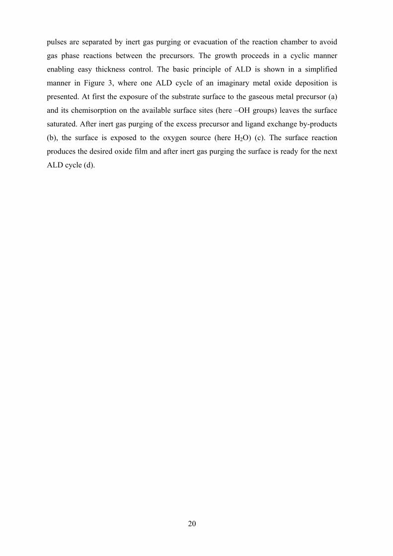
pulses are separated by inert gas purging or evacuation of the reaction chamber to avoid
gas phase reactions between the precursors. The growth proceeds in a cyclic manner
enabling easy thickness control. The basic principle of ALD is shown in a simplified
manner in Figure 3, where one ALD cycle of an imaginary metal oxide deposition is
presented. At first the exposure of the substrate surface to the gaseous metal precursor (a)
and its chemisorption on the available surface sites (here –OH groups) leaves the surface
saturated. After inert gas purging of the excess precursor and ligand exchange by-products
(b), the surface is exposed to the oxygen source (here H2O) (c). The surface reaction
produces the desired oxide film and after inert gas purging the surface is ready for the next
ALD cycle (d).

21
Figure 3. Schematic illustration of an ALD cycle of a hypothetical metal oxide process
where precursors, L1ML2 (M=metal, L1,2=ligands, e.g. CH3, Cl, Cp, alkylamide) and H2O
are alternately pulsed and separated by inert gas pulsing. Instead of inert gas pulsing
evacuation of the reaction chamber can be used.
OH OH OH OH
L1
L1 ML2
L2L1
L1
M
ML1
L1
ML1
L1
L2L2
L1L1 M
OH
OH
OH
O
O
OO
O
O
L1
L2
M
ML1
L1 L1L1
MO OO O
ML1 L1
HO
HO
HO
MO O O O
M M
M
O
O
O O
O
O
H
MOH
OH
OH
OH
OH
HL2
HL1
HL2HL2
HL2
HL1
HL2
HL2
HL2
HL2
N2 N2N2N2
N2N2
N2N2
N2
N2
L2
MO O O O
ML1 L1
L1 L1
M
ML1
L1
O
O
O O
O
O
H2OH2O
H2O
H2O
H2O H2O H2O
H2OH2O
H2O
H2OH2O
L1 L1
HL1HL1HL1
HL1 HL1
N2N2
N2N2N2
N2N2
N2N2 N2
N2
N2
N2
N2HL1
HL2
HL1
HL1
M
(a) Metal precursor pulse on the OH-terminated surface
(b) Metal precursor adsorbed, HL1 and HL2 released and purged by inert N2
(c) H2O pulse
(d) HL1 and HL2 released and purged by inert N2, surface ready for next the ALD cycle
OH
L2
L2
L2
L2
L2L2
L2
L1
ML1
OHOH OH OH
N2N2
L2
L2
ML1
L1
H2O
Nex
t cyc
le
OH
HL1
22
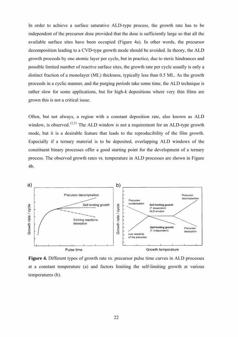
In order to achieve a surface saturative ALD-type process, the growth rate has to be
independent of the precursor dose provided that the dose is sufficiently large so that all the
available surface sites have been occupied (Figure 4a). In other words, the precursor
decomposition leading to a CVD-type growth mode should be avoided. In theory, the ALD
growth proceeds by one atomic layer per cycle, but in practice, due to steric hindrances and
possible limited number of reactive surface sites, the growth rate per cycle usually is only a
distinct fraction of a monolayer (ML) thickness, typically less than 0.5 ML. As the growth
proceeds in a cyclic manner, and the purging periods take some time, the ALD technique is
rather slow for some applications, but for high-k depositions where very thin films are
grown this is not a critical issue.
Often, but not always, a region with a constant deposition rate, also known as ALD
window, is observed.12,31 The ALD window is not a requirement for an ALD-type growth
mode, but it is a desirable feature that leads to the reproducibility of the film growth.
Especially if a ternary material is to be deposited, overlapping ALD windows of the
constituent binary processes offer a good starting point for the development of a ternary
process. The observed growth rates vs. temperature in ALD processes are shown in Figure
4b.
Figure 4. Different types of growth rate vs. precursor pulse time curves in ALD processes
at a constant temperature (a) and factors limiting the self-limiting growth at various
temperatures (b).

23
In addition to the above-mentioned applications in microelectronics, ALD certainly offers
potential solutions in many other areas, such as optics and optoelectronics,
nanotechnology, micro-electromechanical systems, catalysis, magnetic recording head
technology, and protective and antireflective coatings.9
1.3 Precursor chemistry in ALD of oxide films
Besides having an efficient reactor with uniform gas distribution within the reaction
space,32 careful selection of the precursor is of an utmost importance for a successful ALD
process. The main requirements for a good ALD precursor can be listed as follows. The
precursor must be sufficiently volatile and must not undergo significant self-decomposition
at deposition temperature, a problem which leads to a CVD-type growth mode. The
precursor must adsorb or react with the surface sites, and its reactivity must be sufficient
also towards the oxygen source. In contrast to CVD, the ∆G value for the reaction should
be as negative as possible.9 Furthermore, the precursor and its reaction by-products should
not etch the surface or the growing film. Important factors include also practical aspects,
such as safety and economical requirements.9,12 In addition, liquid or gaseous precursors
are generally preferred over the solid ones.
1.3.1 Metal precursor types
The various metal precursor types applied in ALD of oxide films are schematically
presented in Figure 5. Here, the metal precursor types are introduced only briefly; more
detailed examples of the precursors used for high-k materials will be presented in Section
1.4.
The most common group of inorganic precursors in ALD are the halides, where the metal
atom is bonded to halogen atoms (F, Cl, Br or I). For example, HfCl4 together with water is
one the most frequently studied ALD process and will be discussed in more detail in
Section 1.4.2. The beneficial characteristics of many metal halides include their high
thermal stability over a wide temperature range, good reactivity and wide availability as
volatile compounds for many metals. Furthermore, they are readily available and/or can be
easily synthesized. However, drawbacks include possible generation of particles and
corrosive by-products as well as halide contamination in the deposited films. Other purely

24
inorganic precursors are occasionally used despite their limited stability, for instance, the
metal nitrates.33
Alkoxides, where the metal ion is bonded to the oxygen, have been frequently applied for
the ALD of various oxide films. However, thermal stability of the alkoxides is limited and
ALD-type growth mode is not often achieved.34,35,36 The β-diketonates, used frequently in
CVD,37-39 have also been studied for the ALD of RE oxide films.40,24 Because the C-O
bond is relatively strong, powerful oxidizers are needed, but still, some carbon is left in the
film.24 In addition, steric hindrance, caused by the bulky size of the ligands results in low
growth rates. It should be noted, though, that for the rare earth oxides not many other types
of viable precursors exist and thus the β-diketonates form an important group of precursors
in ALD of RE oxides.24
Figure 5. Examples of precursor types applied in the ALD of oxide thin films. The R’s
represent alkyl groups such as methyl (Me) or ethyl (Et).
Among the precursors where the metal is bonded to nitrogen, dialkylamido (alkylamides)
and amidinato complexes have recently gained attention.10,41 Alkyl amides are volatile and
reactive towards water, which makes the group interesting as precursors for high-k
M
O
R
M
X
M
R
M
NR
Rn
nn
n
M
OO
RR
n
nR
R
NN
M
Rn
M
Halides(X=F, Cl, Br, I)
Alkoxides β-diketonates Alkyls
Cyclopentadienyls Alkylamides Amidinates

25
materials. However, as described in Section 1.4.1 the thermal stability can be a problem in
some cases. The self-decomposition of the precursor seems to be affecting the growth
characteristics also in the case of amidinates.42
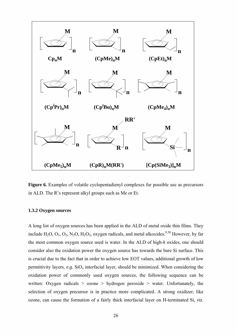
The true organometallics, viz. the metal alkyls and cyclopentadienyl compounds, can be
exploited in ALD for high quality film growth. For example, AlMe3/H2O is an excellent
ALD process for the deposition of Al2O3.30 Alkyls are highly volatile and reactive but their
availability is rather limited and presently they are used as precursors for Al and Zn
containing films.30,43 Cyclopentadienyl or metallocene compounds, having at least one
direct metal-carbon bond to the Cp-ligand (C5H5), offer a wider range of possibilities as
precursors. The Cp-compounds, first synthesized in the 1950s,44,45 are generally volatile
and highly reactive, and thus suitable as ALD precursors.46 Cp-compounds have been
previously applied for various ALD processes (see the recent review by Putkonen and
Niinistö46), but not extensively for high-k gate oxide depositions. They have also been
applied as catalysts,47 and thus the commercial availability in many cases is good. Often,
however, thermal stability is limited, but a wide variety of different substituents exists as
seen in Figure 6.
26
Figure 6. Examples of volatile cyclopentadienyl complexes for possible use as precursors
in ALD. The R’s represent alkyl groups such as Me or Et.
1.3.2 Oxygen sources
A long list of oxygen sources has been applied in the ALD of metal oxide thin films. They
include H2O, O3, O2, N2O, H2O2, oxygen radicals, and metal alkoxides.9,30 However, by far
the most common oxygen source used is water. In the ALD of high-k oxides, one should
consider also the oxidation power the oxygen source has towards the bare Si surface. This
is crucial due to the fact that in order to achieve low EOT values, additional growth of low
permittivity layers, e.g. SiOx interfacial layer, should be minimized. When considering the
oxidation power of commonly used oxygen sources, the following sequence can be
written: Oxygen radicals > ozone > hydrogen peroxide > water. Unfortunately, the
selection of oxygen precursor is in practice more complicated. A strong oxidizer, like
ozone, can cause the formation of a fairly thick interfacial layer on H-terminated Si, viz.
M
RR'
M M
M M M
M
Si
MM
nn n
n n n
nnR n
CpnM (CpMe)nM (CpEt)nM
(CpiPr)nM (CptBu)nM (CpMe4)nM
(CpMe5)nM (CpR)nM(RR') [Cp(SiMe3)]nM

27
approximately or usually more than 1 nm,48-50,II,V which may preclude ozone-processing as
a long-term solution for gate dielectric fabrication. On the other hand, when compared to
water, ozone can produce denser films with lower impurity levels and enhanced electrical
properties.50,51 Water-based processes rely on hydroxyl groups on the starting surface and
high reactivity of the chemisorbed metal precursor towards the water pulse, otherwise the
initial nucleation of the deposited films may be inhibited resulting in poor electrical
properties of the deposited film.52,53 In many cases, the metal precursor is not reactive
enough towards the oxygen source and a stronger oxygen source must be used to deposit
good quality film.54 Until recently, comparative studies on the use of different oxygen
sources in ALD of high-k oxides were seldom performed. One aim of this study was to
evaluate the usability of ozone in ALD of high-k oxides and the results obtained will be
discussed in detail in Chapter 3.
1.4 ALD of high-k dielectrics
As mentioned in Section 1.1, the leading candidates for alternative high-k dielectrics are
the oxides, silicates, and silicate oxynitrides of Zr and Hf, as well as the oxides of the rare
earths. As the selection of the precursor has an effect on the characteristics of the deposited
film, this section emphasizes processes for the binary oxides, such as ZrO2 and HfO2, that
are deposited with different types of precursors, and describes the current status of these
materials. In this context, the Zr and Hf-based silicates are only briefly mentioned. Also,
the less studied field of rare earth oxides by ALD will be discussed.
1.4.1 ZrO2
The first ALD study on ZrO2 published was the ZrCl4/H2O process.55 In that study, the
growth temperature applied was 500°C, yielding a growth rate of 0.53 Å/cycle. Since then
several groups have applied the same process in a wide temperature range of 180 to
600°C.52,56-60 The optimized temperature found in most studies is 300°C, showing well-
saturated growth with a growth rate of 0.5-1.0 Å/cycle, the exact value depending on the
reactor set-up. Hydrogen and chlorine impurity levels at 300°C have been reported to be
0.6-0.8 and 1.5 at-%, respectively.57 The chlorine level could be reduced by annealing at
high (900-1050°C) temperatures.61 However, annealing caused crystallization even in very
thin layers.62 The chlorine residues tend to accumulate at the interface region between the
film and Si substrate.63 Problems related to the ZrCl4/H2O process include also the fact that

28
the metal precursor, being a fine solid, can generate particle contamination and the ALD
reaction by-product is corrosive HCl.64 In addition, the inhibited growth of zirconia on H-
terminated Si, leading to an island-type growth,52,65 remains as a challenge. A common
solution to overcome this problem is to use thin thermal or chemical SiO2 or nitrided SiO2
as a starting layer. However, as lower k interfacial layer is introduced, to achieve sub-1.0
nm EOT values with low leakage becomes more difficult. For these obvious reasons
alternative chemistries for the ALD of ZrO2 has been the subject of much research. The
reported ALD processes of ZrO2 are listed in Table 2, including details of growth
temperatures and impurities.
An option instead of using ZrCl4 is to employ another Zr halide, namely ZrI4.66-69
Unfortunately especially for the high-k dielectric applications, ZrI4 does not bring about
any significant remedy to the problems mentioned above. The halide content remained at
least at the same level as in the case of ZrCl4 but presumably due to the weaker metal-
halogen bond strength the annealing reduced the halide content more effectively.70 On the
other hand, it was observed that desorption of iodine caused problems for saturation of
growth at 300°C.67
A distinct benefit of using Zr alkylamides, such as Zr(NMe2)4, Zr(NEtMe)4, and Zr(NEt2)4
is that they are liquid at the evaporation temperature eliminating the particle contamination
problem.71 Furthermore, the alkylamides are reactive towards water and give impurity
levels that are at least for C and N reasonably low, e.g. below 1 at-% for C.71 However,
higher C contents have been reported when oxygen or oxygen plasma was used as the
oxygen source.72-75 The problematic issue in the use of alkylamides is their thermal
stability; e.g. for the Zr(NMe2)4/H2O process, the precursor decomposition limits the
maximum growth temperature to 250°C. Furthermore, the growth temperature must be low
if smooth films are desired.76
From the family of silylamide precursors, ZrCl2[N(SiMe3)2]2 has been applied together
with H2O to process zirconia yielding films with a few at-% of Si but low contents of C, H,
and Cl.77
The limited thermal stability of Zr alkoxides represents a problem for their use in ALD.
For instance, Zr(OtBu)4 has been employed with several oxygen sources78-80 and even with

29
oxygen plasma,72,81,82 but true ALD growth could not be achieved due to thermal
decomposition of the metal precursor.78,82 The decomposition behavior correlated with the
impurity contents; 5-8 at-% of C has been reported for films deposited even at very low
temperatures. Other approaches, like replacing two -OtBu ligands with
dimethylaminoethoxide (dmae) ligands only slightly improved the thermal stability and
self-limiting growth was not achieved.83,84 Other solutions using the dmae-ligands were not
successful, either.83
From the β-diketonate precursor group, Zr(thd)4 has been used to grow ZrO2 films.85
Because of the low reactivity of the precursor, ozone was required as the oxygen source,
but still a growth rate of only 0.24 Å/cycle was reported at deposition temperature of 375-
400°C. ALD-type growth was confirmed and the contents of impurities were low, 0.2 and
0.3 at-% for C and H, respectively.
The use of cyclopentadienyl derivatives of Zr for ZrO2 film growth was introduced quite
recently.85,I,II Depositions from either Cp2ZrCl2 or Cp2ZrMe2 together with ozone showed
an ALD-type growth with H and C residues less than 0.5 at-% and ZrO2 growth rate of
0.55 Å/cycle within the ALD window regime, 300-350°C.85 Cp2ZrMe2 could also be
applied together with waterI and this process, including reaction mechanism studiesIII and a
comparison of structural and dielectric properties between the ozone- and water-processed
filmsII is discussed in more detail in Section 3.1.

30
Table 2. Published ALD processes of ZrO2 including growth temperatures and impurity
characteristics.
Precursors Tgrowth Impurities (at preferred Tgrowth)
Metal precursor
Oxygen source
Range, oC
Preferred,oC
C, at-%
H, at-%
Other, at-%
Analysis method
Ref.
halides
ZrCl4 H2O 180-600 300 1.5 Cl: 0.6-0.8 TOF-ERDA 55,57
H2O +
H2O2
180-600
300
N.R.
N.R.
57,58
O2* 500 500 N.R. 86
ZrI4
H2O +
H2O2
230-500
275-325
3-8
I: 0.5-1.2
TOF-ERDA,
XPS
66,68,69
amides Zr(NEtMe)4 H2O < 250 < 250 < 1 N.R. N: < 0.25 RBS 71
O2 a 110-250 200-250 1.6-3 N.R. N: 0.3-3.5 AES, RBS 73
Zr(NMe2)4 H2O < 300 < 300 < 1 N.R. N: < 0.25 RBS 71
Zr(NEt2)4 H2O < 350 < 350 < 1 N.R. N: < 0.25 RBS 71
O2 a 250 250 1-3 N.R. N.R. AES 72
O2 250 250 3-5 N.R. N.R. AES 72
ZrCl2[N(SiMe3)2]2 H2O 150-350 250 N.R. N.R. Si: 4 RBS, SIMS 77
alkoxides Zr(OtBu)4 O2 250 250 6-8 N.R. N.R. AES 72
O2 a 250 250 3-5 N.R. N.R. AES 72,81
H2O 150-300 < 250 8 2 N.R. TOF-ERDA 78
N2O 150-300 < 250 N.R. N.R. N.R. 79
Zr(dmae)4 H2O 190-340 190-340 5 30 N: < 4 TOF-ERDA 83
Zr(OtBu)2(dmae)2 H2O 190-340 190-340 1.7-3 8-13 N: 0.3-1.3 TOF-ERDA 83,84 Zr(OiPr)2(dmae)2 H2O 190-340 190-340 N.R. N.R. N: < 1 TOF-ERDA 83
β-diketonates Zr(thd)4 O3 275-500 375 0.2 0.3 F: < 0.1 TOF-ERDA 85
cyclopentadienyls Cp2ZrMe2 H2O 200-500 350 < 0.1 < 0.1 N.R. TOF-ERDA I
O3 250-500 310-365 0.2 0.1 F: 0.1 TOF-ERDA 85
Cp2ZrCl2 O3 200-500 300 0.5 0.5 Cl: < 0.07 TOF-ERDA 85
* atmospheric pressure, a plasma, N.R. = not reported

31
1.4.2 HfO2
One of the most thoroughly studied ALD processes is the HfCl4/H2O process, first
introduced some 10 years ago.87,88 Clearly, the interest in this process stems from the fact
that in recent years HfO2 has been identified as and continues to be considered one of the
most promising high-k dielectrics.3 Similarly as in the case of the ZrCl4/H2O process, the
obvious drawbacks of HfCl4/H2O are well identified. The chlorine content, which is more
pronounced near the HfO2 film/silicon interfacial region,89 has been reported to cause
etching of the silicon substrate during post-deposition annealing, which contributes to void
defect formation.11 Additional problems include poor nucleation of HfO2 when deposited
directly on Si,90 and formation of particles from the precursor in the gas phase. To
overcome the problems related to the poor nucleation on HF-etched Si, the use of a thin
chemically or thermally grown SiO2, nitrided SiOx, or interfacial layer of Al2O3 made by
ALD has been suggested.90 Nevertheless, additional interfacial layer increases the EOT
value and in an ideal case a sharp interface between the Si and HfO2 would be desirable.
Despite the problems listed above, the HfCl4/H2O process has many attractive features: the
growth temperature range is wide, deposition temperatures ranging from 160 to 940°C
have been reported,91,92 the film quality and uniformity can be optimized over a large
surface area,90 carbon incorporation from the precursor into the films can be ignored, and
good electrical properties, such as substantial leakage current reduction with respect to
SiO2, are well understood.90 Due to the fact that HfCl4/H2O growth process is so well
optimized and established, finding a significantly better process is a challenging task.
The reported ALD processes for HfO2 are listed in Table 3, where the alternative
processes, as expected, are very similar to the previously described alternative ZrO2
processes (Table 2). However, the influence of oxygen source has been studied in more
detail in the case of HfO2. Interestingly, replacing H2O with O3 in the HfCl4-based process
improves most of the dielectric properties, including fixed charge, interface trap densities,
and the leakage current characteristics, as well as decreasing the Cl-content in the bulk of
the film.51 On the other hand, after rapid thermal annealing (RTA) at 750°C, higher oxygen
content in the ozone-processed films resulted in thicker interfacial layer and thus increased
CET. Commonly, the interfacial layer thickness in HfCl4/H2O process at 300°C on HF-
etched Si has been reported to be about 1.0-1.2 nm.93

32
A feasible route to Cl-free films is the use of HfI4 instead of HfCl4. The HfI4/H2O process
yields slightly lower halide content in the films than the conventional HfCl4 process when
applied at 300 °C but the difference is not significant.94 Using the iodide precursor with
molecular oxygen eliminates hydrogen residues but the process requires rather high
temperatures (500-750°C).95,96
The use of volatile, liquid hafnium alkylamides, especially Hf(NEtMe)4, with water can
provide excellent thickness uniformity and conformality71 and excellent nucleation without
significant interfacial layer formation on H-terminated Si,97 but also yields films with
considerable impurity content; e.g. 0.3-0.6 at-% of C and 2-3 at-% of H when
Hf(NEtMe)4/H2O ALD-process was applied at 250 °C.98 The suitable ALD growth
temperature range for the Hf(NEtMe)4/H2O process is reported to be below 350°C71 but
slight decomposition of the precursor was probably affecting the growth rate already at
temperatures around 300°C.98 In another report, where the Hf(NEtMe)4/O3 process was
applied, the maximum growth temperature suitable for good quality HfO2 was 275°C.99
The thickness of the interfacial layer between HfO2 and H-terminated Si has been reported
to be exceptionally low, ~0.5 nm for the Hf(NEtMe)4/H2O process and problems in
nucleation at early stages of the growth were not detected.97 Interestingly, reaction with
surface Si-H is initiated by the metal precursor, and not by the oxygen source.100 It is worth
noting that hydroxyl groups are incorporated into the HfO2 film.100 The interfacial SiO2
then forms during annealing. Ozone as the oxygen source instead of water has gained
considerable interest also in the case of Hf(NEtMe)4 precursor to grow HfO249,93,99,101,102
and especially together with a suitable Si-source, Hf-silicate.22,102,103,104 However, in some
studies the use of ozone did not significantly reduce impurities nor enhance electrical
properties as compared to the use of water.93,101 As compared with Hf(NEtMe)4, higher
impurity levels were detected in films obtained from Hf(NMe2)4 and water105 or ozone.115
Signs of thermal decomposition of the Hf(NMe2)4 precursor were detected already at
250°C.105 In addition, the surface roughness increased rapidly at temperatures around
250°C.76 When using the Hf(NMe2)4/H2O process, it was recently proposed that during the
early stages of HfO2 growth on H-terminated silicon, a SiNx interfacial layer is formed
instead of SiO2, thus yielding a very promising CET of 1.8 nm with low leakage current
density.107 However, in another study a relatively thick 1.5-2.0 nm interfacial silicon oxide
layer was observed between Si and amorphous HfO2.105 Using ozone instead of water at a
relatively high growth temperature of 300°C reduced the impurity contents and the films
33
showed a more amorphous structure leading to better leakage current characteristics.108,109
A third Hf-alkylamide precursor, Hf(NEt2)4, has been used occasionally, together with
either water,71,110 oxygen,111 or oxygen plasma111-114 as the oxygen source. Especially in
the case of oxygen plasma, the growth of interfacial Hf-silicate layer can be
significant.111,112
As in the alternative ZrO2 processes, the alkoxide-based processes of HfO2 generally suffer
from poor thermal stability of the Hf-precursor.81,82,115-119 Due to the decomposition of the
precursor, carbon and hydrogen impurities remain high, e.g. the ALD process employing
hafnium tetrakis(1-methoxy-2-methyl-2-propanolate), Hf(mmp)4 with H2O at 360 °C
resulted in as-deposited films with 12 and 6 at-% of C and H, respectively.118
Anhydrous volatile Hf(NO3)4 has also recently been applied as an ALD precursor for the
deposition of oxygen-rich hafnium oxide films.33,120 A promising CET value of 2.1 for a
5.7 nm film deposited directly on H-terminated Si was reported, but the precursor
decomposition limits its use to only very low temperatures of 180 °C or lower.33
Another precursor family exhibiting both high reactivity and volatility are the
cyclopentadienyl compounds of hafnium, which have recently been introduced in ALD for
high quality HfO2 film growth.IV,V Section 3.2 describes the growth characteristics and
HfO2 film properties obtained with the Cp-based hafnium processes. For comparison,
compositional data of the films deposited with the Cp-precursors are also included in the
Table 3.

34
Table 3. Published ALD processes for HfO2 with reported impurities.
* atmospheric pressure, a plasma, N.R. = not reported
Precursors Tgrowth Impurities (at preferred Tgrowth)
Metal precursor
Oxygen source
Range, oC
Preferred,oC
C, at-%
H, at-%
Other, at-%
Analysis method Ref.
halides
HfCl4 H2O 160-940 300 0.5-1.5 Cl: 0.4 TOF-ERDA 51,88,90-92,94
O3 300 300 N.R. N.R. 51
O2* 250-650 550-650 Cl: 0.1 XPS, SIMS 121
Hf(NO3)4 150-190 150-190 N.R. N.R. 122
HfI4 H2O 225-500 300 1.5 I: 0.4 TOF-ERDA 94
O2 400-755 570-755 < 0.1 I : < 0.1 TOF-ERDA 95,96
amides
Hf(NEtMe)4 H2O 100-450 250 0.3-0.6 2-3 N: < 0.2 TOF-ERDA 71,98
O3 100-400 250-300 1.5 N.R. N.R. AES 115
Hf(NMe2)4 H2O 100-500 250 1.5 6 N: < 0.7 TOF-ERDA 71,105,123
O3 160-420 200-300 4.5 N.R. N.R. AES 115
Hf(NEt2)4 H2O 100-500 <450 < 1 N.R. N: < 0.25 RBS 71
O2 250 250 5 N.R. N.R. AES 111
O2a 250 250 2.5 N.R. N.R. AES 111
HfCl2[N(SiMe3)2]2 H2O 150-250 200 < 1 < 1 N: < 1 AES 124
alkoxides
Hf(OtBu)4 O2 350-480 350-480 N.R. N.R. N.R. 116
O3 300-450 300 6 N.R. N.R. AES 115,125,126
O2a 200-250 200 N.R. N.R. N.R. 82
Hf(OtBu)2(mmp)2 H2O 275-400 360 2.7 11 N.R. TOF-ERDA 117
Hf(mmp)4
H2O
225-450
225-360
0.8-6
12
N.R.
TOF-ERDA, AES
118,127
Hf(ONEt2)4 H2O 250-350 300 6 11 N: < 1 TOF-ERDA 119
cyclopentadienyls
Cp2HfMe2 H2O 300-500 350 0.4 0.2 N.R. TOF-ERDA IV,V
O3 275-450 350 < 0.1 < 0.1 N.R. TOF-ERDA V
Cp2HfCl2 H2O 350 350 1.2 0.5 Cl: 0.4 TOF-ERDA V
O3 350 350 < 0.3 < 0.3 Cl: < 0.1 TOF-ERDA V
Other
Hf(NO3)4 H2O 160-190 180 N.R. N: 1.2 XPS 33,120

35
1.4.3 Rare earth oxides
The ALD of rare earth oxides generally suffers from the lack of suitable precursors. The
first ALD processes for RE oxides were reported in the early 1990s, introducing β-
diketonate precursors together with a strong oxygen source, ozone, to grow Y2O3128 and
CeO2129 films. Since then new classes of precursors have been introduced which can be
conveniently divided into three categories according to the ligand donor atom; namely
oxygen-, carbon-, and nitrogen-coordinated precursors. Here the reported RE oxide
processes are considered only briefly, a more detailed survey has been recently reported by
Päiväsaari et al.130 For more specialized reviews emphasizing gate dielectrics in
microelectronics, see also Leskelä et al.131,132
Typically the existing RE oxide ALD processes have been based on the oxygen-
coordinated β-diketonate precursors, such as the thd-complexes (thd=2,2,6,6-tetramethyl-
3,5-heptanedione) from which almost all RE binary oxides, except the oxides of Pr, Pm
and Tb, have been grown.24,48,128,129,133-138,VIII As thd-compounds are not reactive enough
towards water, ozone was required as oxygen source. Typically the deposition temperature
for an optimized RE oxide ALD process has been 300°C.24 Interestingly, it was reported
that growth rate at 300°C increased linearly as a function of the ionic radius of the
lanthanides, suggesting the same growth mechanism regardless of the metal.24 The
RE(thd)x/O3 processes generally produce oxygen deficient films with C and H impurities
around 1-5 and 1-2 at-%, respectively.24 Deviations in the carbon content are caused by the
difference in basicity of the RE oxides, resulting in large content of carbonate-type
impurities for the larger ions, e.g. La2O3 contained up to 10-12 at-% of carbon,134 but
Sc2O3 only less than 0.1 at-%.133 The growth rates in thd-based RE oxide processes are
generally low, caused by the considerable steric hindrance and low reactivity. To increase
the growth rates radical enhanced ALD has also been applied.139,140 Unfortunately, carbon
content was thereby further increased, up to 26 at-% in Er2O3 films.139 Oxygen-coordinated
precursors other than those based on the thd ligand have been only occasionally applied,
e.g. ALD of Gd2O3 and PrOx from Gd(mmp)3 and Pr(mmp)3 with water as oxygen source
was recently reported.127 Unfortunately, self-limiting growth was not achieved due to
precursor decomposition.
36
Among the nitrogen-coordinated precursors, silylamides and amidinates have especially
gained recent interest as potential ALD precursors. Silylamide compounds of La, Gd and
Pr may provide a feasible route to grow high-k La2O3,123,141-143 Gd2O3,35,36 and PrOx144
films. At least in the case of Ln[N(SiMe3)2]3/H2O (Ln=Gd,Pr) processes, self-limiting
growth could not be observed due to the precursor decomposition, resulting also in
considerable impurity contents.35,36,144 The La[N(SiMe3)2]3/H2O process, however, was
reported to be saturative at 200-275°C, but about 10 at-% of Si was determined to be
present in the deposited films.142 In another recent study, the thermal decomposition of
La[N(SiMe3)2]3 could not be excluded as a possible factor affecting the growth behavior.145
Another interesting approach to ALD of RE oxide films is based on the use of amidinate
complexes of the composition RE[RamdR]x (R=alkyl group, amd=NC(CH3)N). The
[iPramdiPr]3 complexes of Y, Sc, La have been applied by Gordon and coworkers using
water to form Y2O3,146 Sc2O3,147 and La2O341 films. In a more detailed report, the Y2O3
process was found to be promising, as the conformality and dielectric properties were
good.146 Thermal stability may call for attention, as Y[iPramdiPr]3 decomposition became
evident at temperatures exceeding 280°C.146 In another study, Er2O3 films were grown
using Er[tBuamdtBu]3 and ozone.42 Water was not reactive enough as an oxygen source,
because of higher steric hindrance caused by the tert-butyl groups compared to the iso-
propyl groups. On the other hand, tert-butyl groups should be more protective towards
decomposition of the complex and thus the thermal stability should be better.148 However,
self-limiting growth of Er2O3 could not be achieved due to the probable partial
decomposition of Er[tBuamdtBu]3, considering that upon increasing the precursor pulse
length the growth rate also increased.42 One possible reason for this behavior was
suggested: In the Y[iPramdiPr]3/H2O process, the adsorption of some water during the
water pulse followed by desorption of water could result in a water-rich ambient above the
film. This would lead to a CVD-type growth if purging times are not very long.146
Therefore, purge time for water used in the Y[iPramdiPr]3/H2O study was 60 s.146
However, a 5-fold increase in purge times in the Er[tBuamdtBu]3/O3 process did not have
any effect.42 On the other hand, in ozone processes the growth mechanism is different than
in water processes. Generally, very long purge times would make a process practically
unfit for applications, but at the same time, dielectric properties could be enhanced due to
the annealing effect achieved during the deposition.
37
Interest in true organometallic compounds for application in ALD of RE oxides is
currently focused on the cyclopentadienyl compounds. As suitable metal alkyls do not
exist for rare earths, volatile and reactive Cp-compounds have been applied in several RE
oxide growth studies.133,VII-IX,149 More detailed discussion on the applicability of RE Cp-
compounds as well as an introduction to various REScO3 processes are presented in
Section 3.3.
38
2. EXPERIMENTAL
This chapter briefly presents the methods used for film growth studies and for the
characterization of the deposited films, as well as explains how the in situ reaction
mechanism studies were performed. More detailed descriptions including, when relevant,
precursor synthesis, properties and pulsing sequences can be found in the original
publications I-IX. For the processes not reported earlier, the growth characteristics are
described in chapter 2.1.
2.1 Precursors and film growth
High-k oxide films were deposited in a commercial flow-type hot-wall ALD reactor (ASM
Microchemistry F-120). As precursors, thd- or cyclopentadienyl-type compounds were
applied together with the oxygen source (O3 or H2O). Because of their air and moisture
sensitivity, the cyclopentadienyl precursors were handled in an Ar glove box and inertly
inserted into the reactor. The metal precursors were evaporated from an open glass crucible
inside the reactor. Ozone was generated from O2 (99.999%) in an ozone generator (Fischer
model 502). The ozone concentration as determined by iodometric titration was about 4
%.133 Water was evaporated from a container kept at 25°C. Precursors used in this study
are listed in Table 4, where also their origin and the evaporation temperatures are shown.
Depositions were carried out at 2-3 mbar pressure. Nitrogen (99.999%) was used as a
carrier and purging gas except in the reaction mechanism studies, where Ar (99.999%) was
used. As substrates, p- or n-type Si(100) (Okmetic, Finland) and sodalime glass were used.
The substrate area was 10 x 5 cm2. HF-etching of the Si-substrate immediately prior to the
deposition was applied in selected experiments in order to remove the native SiO2. The
standard pulsing sequence for the binary water-based processes where as follows: 1.0-1.5 s
metal precursor pulse, 1.5 s purge, 1.5 water pulse, 1.5 s purge. When ozone was applied,
the oxygen source pulse time and the following purge time were both 2.0 s. The metal
precursor pulse time was varied between 1.0 and 3.0 s in order to study the saturation
characteristics. For the novel ternary processes, GdScO3 and ErScO3, the pulsing sequence
was similar as that used for YScO3.IX
39
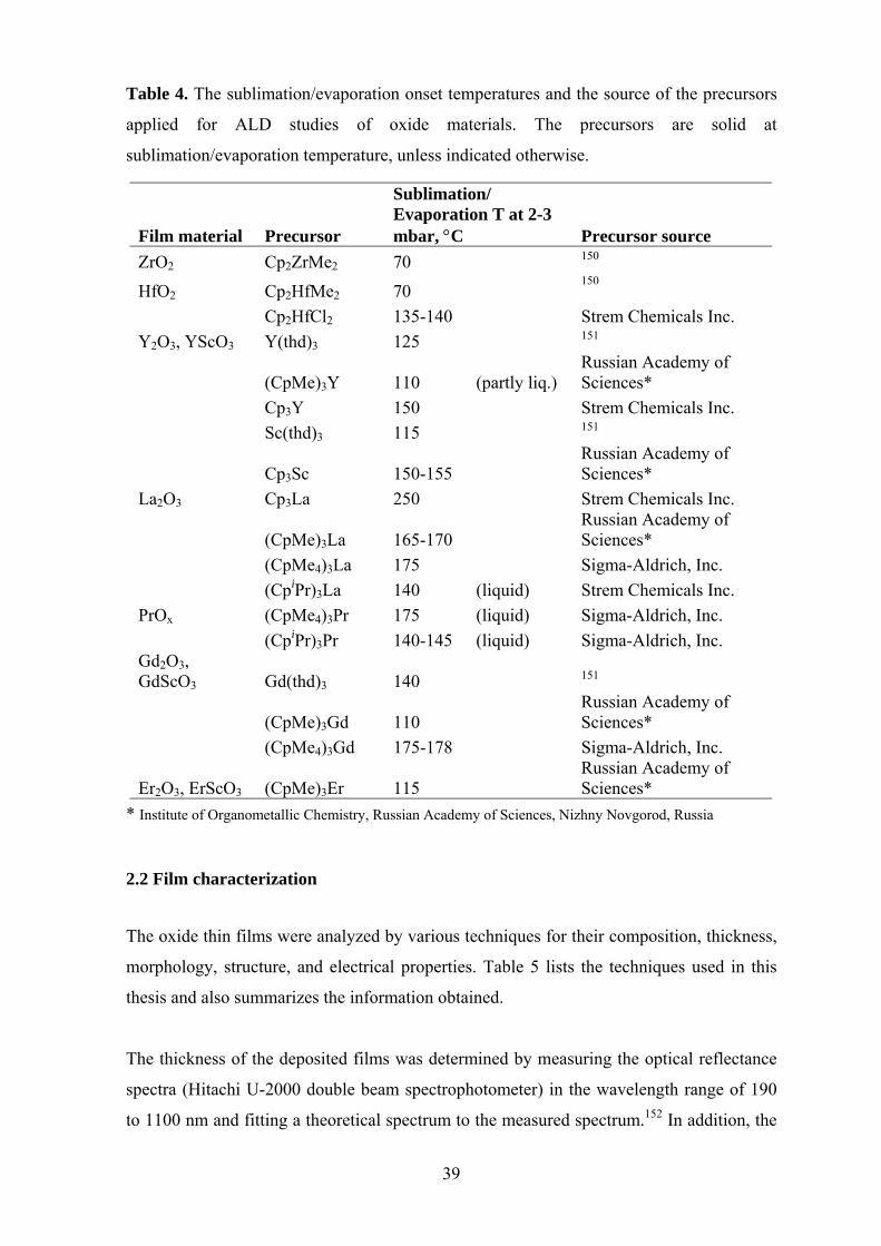
Table 4. The sublimation/evaporation onset temperatures and the source of the precursors
applied for ALD studies of oxide materials. The precursors are solid at
sublimation/evaporation temperature, unless indicated otherwise.
Film material Precursor
Sublimation/ Evaporation T at 2-3 mbar, °C Precursor source
ZrO2 Cp2ZrMe2 70 150
HfO2 Cp2HfMe2 70 150
Cp2HfCl2 135-140 Strem Chemicals Inc. Y2O3, YScO3 Y(thd)3 125 151
(CpMe)3Y 110 (partly liq.) Russian Academy of Sciences*
Cp3Y 150 Strem Chemicals Inc. Sc(thd)3 115 151
Cp3Sc 150-155 Russian Academy of Sciences*
La2O3 Cp3La 250 Strem Chemicals Inc.
(CpMe)3La 165-170 Russian Academy of Sciences*
(CpMe4)3La 175 Sigma-Aldrich, Inc. (CpiPr)3La 140 (liquid) Strem Chemicals Inc. PrOx (CpMe4)3Pr 175 (liquid) Sigma-Aldrich, Inc. (CpiPr)3Pr 140-145 (liquid) Sigma-Aldrich, Inc. Gd2O3, GdScO3 Gd(thd)3 140 151
(CpMe)3Gd 110 Russian Academy of Sciences*
(CpMe4)3Gd 175-178 Sigma-Aldrich, Inc.
Er2O3, ErScO3 (CpMe)3Er 115 Russian Academy of Sciences*
* Institute of Organometallic Chemistry, Russian Academy of Sciences, Nizhny Novgorod, Russia
2.2 Film characterization
The oxide thin films were analyzed by various techniques for their composition, thickness,
morphology, structure, and electrical properties. Table 5 lists the techniques used in this
thesis and also summarizes the information obtained.
The thickness of the deposited films was determined by measuring the optical reflectance
spectra (Hitachi U-2000 double beam spectrophotometer) in the wavelength range of 190
to 1100 nm and fitting a theoretical spectrum to the measured spectrum.152 In addition, the

40
thickness, roughness, density and crystal structure of selected ultrathin films were
evaluated by X-ray reflectometry (XRR) and by grazing incidence X-ray diffraction (GI-
XRD) using a Bruker D8 Advance X-ray diffractometer. Crystallite orientations and
crystallinity of the deposited films were determined by X-ray diffraction with Cu Kα
radiation in a Philips MPD 1880 diffractometer. High-resolution transmission electron
microscopy (HR-TEM) was also applied in order to examine the cross-section of an
ultrathin sample as well as the interfacial layers between selected deposited films and the
silicon substrate. The high-resolution images were obtained with a field emission gun
TECHNAI F30 ST or Hitachi: H9000NAR, both operated at 300 kV. To investigate the
composition of the interfacial layer, X-ray photoelectron spectroscopy (XPS) was applied.
The measurements were carried out in an AXIS 165 spectrometer (Kratos Analytical)
using monochromated Al Kα irradiation at 100 W. Surface morphology was studied with a
Nanoscope III atomic force microscope (AFM), by Digital Instruments, operated in
tapping mode. Roughness values were calculated as root mean square (rms) values.
Film compositions were measured by time-of-flight elastic recoil detection analysis (TOF-
ERDA)153 at the Accelerator Laboratory of the University of Helsinki, Finland and at
IMEC (Interuniversity Microelectronics Center), Leuven, Belgium. For these TOF-ERDA
studies, 53 MeV 127I10+ or 16 MeV 63Cu7+ ion beams were used. Metal to metal ratio in
scandate films were also analysed by XRF (Philips PW 1480) using Rh excitation. In order
to obtain more information on residual carbon and hydrogen impurities, the films were also
analyzed by Fourier-transform infrared (FTIR) spectroscopy. The FTIR single-beam
transmission spectra were collected from the samples deposited on Si with Nicolet Magna-
IR 750 spectrometer.
For electrical characterizations, aluminum gate electrodes for ohmic contact were formed
by e-beam evaporation onto the HF-etched backside of the substrate as well as through a
shadow mask onto the film surface. The resulting capacitor structures were then measured
with a HP 4284A precision inductance-capacitance-resistance-meter and Keithley 2400
source meter to obtain capacitance-voltage (C-V) and leakage current density-voltage (I-V)
characteristics, respectively. The effective permittivity values were calculated from the
accumulation capacitance using equation (1) and thus the CET values and the permittivity
for the high-k layer only from equations (2) and (3).

41
Table 5. Film characterization techniques used.
Technique Information obtained Publication
AFM Surface morphology I, II, IV-IX
Electrical measurements
C-V Dielectric properties I, II, IV-IX
I-V Leakage current I, II, IV-IX
FTIR Carbonate and hydroxide
impurities I, VI, VIII, IX
GI-XRD Crystallinity I, II
HR-TEM Interfacial layer, microstructure I, II, V
QMS Reaction mechanism III
Spectrophotometer Thickness I, IV-IX
TOF-ERDA Impurities, stoichiometry I, IV-IX
XPS Interfacial layer composition II
XRD Crystallinity, crystalline phases I, II, IV-IX
XRF Stoichiometry IX
XRR Thickness, density, interface I, II, IV, V, IX
2.3 Reaction mechanism studies
Experiments to resolve the reaction mechanism for the ZrO2 process from Cp2ZrMe2
precursor were carried out in a commercial, but specially modified, flow-type F-120 ALD
reactor. The reaction chamber was loaded with glass substrates in order to form narrow gas
flow channels between them with large substrate area. To maximize the amount of reaction
by-products, the total area of glass substrates was about 3500 cm2. The gas phase species
were measured with a Hiden HAL/3F 501 RC quadrupole mass spectrometer (QMS) using
an electron multiplier detector, mass range of 1 - 510 amu and ionization energy of 70 eV.
The sampling and the pressure reduction from about 2 mbar to below 10-6 mbar were
accomplished through a 200 µm opening. Instead of H2O as the oxygen source, D2O was
used in order to better distinguish the reaction by-products from the species formed in the
ionizator.

42
Weak background signals arise also even when no exchange reactions should take place,
i.e. when subsequent pulses of only one precursor are given. This background signal,
suggested to be caused by a condensation effect of the metal precursor, pressure change
effects, insufficient mass resolution of the QMS or possible rearrangement reactions during
ionization,154 is subtracted from the signals obtained during the actual ALD process. The
thermal stability of the Cp2ZrMe2 precursor was studied also with the QMS by pulsing
only the precursor and monitoring the ligand decomposition products detected as a
function of deposition temperature.

43
3. RESULTS AND DISCUSSION
This chapter summarizes the main results of ZrO2, HfO2, and rare earth oxide film growth
and characterization. Details for the published processes can be found in the corresponding
publications.I-IX
3.1 ZrO2 from cyclopentadienyl precursor
ALD-type self-limiting growth was achieved by applying Cp2ZrMe2 and H2O as
precursors.I The growth rate increased as a function of deposition temperature and a
distinct ALD window was not observed. At the optimized deposition temperature of 350°C
the growth rate was 0.43 Å/cycle resulting in polycrystalline films. The monoclinic phase
was the dominant one, but minor intensity reflections belonging to the orthorhombic phase
were also observed. At growth temperatures lower than 300°C the growth rate remained
low, indicative of insufficient thermal energy to promote fast surface reactions. At
temperatures exceeding 400°C, poor uniformity of the films was observed due to precursor
decomposition. Interestingly, the roughness of 100-130 nm thick films decreased when the
deposition temperature was increased from 375 to 400°C. At 350°C the impurity contents
for the stoichiometric ZrO2 films were below the detection limit (~0.1 at-%) of TOF-
ERDA for both C and H. The impurity levels were lower than most of the other known
ZrO2 ALD processes (see Table 2). It is worth noting, that the present Cp2ZrMe2/H2O
process results in films with good thickness uniformity over large substrate areas, as
demonstrated in scale-up tests on 200 mm Si wafer (Figure 7).

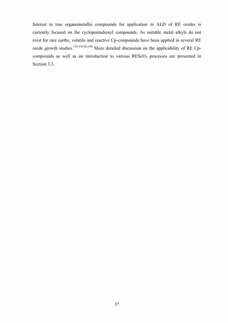
44
Figure 7. The variation of thickness in ZrO2 thin film deposited by ALD at 300°C by the
Cp2ZrMe2/H2O process on 200 mm Si-wafer. The mean thickness of the ZrO2 layer is 38.2
nm and the standard deviation 0.80 %. (Courtesy of ASM Microchemistry Ltd.)
When ozone was applied as the oxygen source, the growth rate of ZrO2 films increased to
0.55 Å/cycle.II Ozone, being a more aggressive oxidant than water, had a strong effect on
the growth behavior, structure, and electrical properties, especially when ZrO2 was
deposited on H-terminated (HF-etched) Si. When water was used as the oxygen source, a
strong inhibition of film growth at the early stages of the deposition process was clearly
detected. As seen in Figure 8, ozone oxidizes the bare Si surface, creating an interfacial
SiOx layer, which is a suitable surface for the film growth to proceed. Water, however, is
not able to form OH-saturated surface for the metal precursor to react with and thus
retarded nucleation leads to island-like growth and reduced density (Figure 8).II

45
Figure 8. HR-TEM images of the ZrO2 films deposited onto HF-etched Si(100) by the
(top) Cp2ZrMe2/O3 (ZrO2 thickness 3.8 nm, IL thickness 1.9 nm) and (bottom)
Cp2ZrMe2/H2O (ZrO2 thickness: 2.1 nm, IL thickness 2.9 nm) process.II
Inhibition of growth has also been detected with the other ZrO2 processes where water is
used as the oxygen source.52 The interfacial layer formed in the water-processed films,
according to the electrical and XPS measurements, is suggested to be a mixture of SiOx
and ZrO2 rather than Zr-silicate.II Similar intermixing in the interfacial layer has been
observed previously, when ZrCl4/H2O process was applied on chemical SiO2.56
The oxygen source and substrate pretreatment had a distinct effect on the electrical
properties of the Al/ZrO2/native SiO2 or HF-etched/n-Si(100) capacitor structures. The
hysteresis width was extremely low for both H2O- and O3-processed HfO2 films on HF-
etched Si (Figure 9). With both processes, the as-deposited films showed flatband voltage
(VFB) shift; in O3-processed films towards negative bias and in H2O-processed films
towards positive bias. Forming gas annealed (5 % H2, 400°C, 30 min) O3-processed
samples exhibited almost the ideal value of VFB. Annealing also reduced the interface state
density values. The permittivity of an 8.8 nm O3-processed film was approximately 20.

46
The Cp2Zr(CH3)2/H2O process on native oxide-free Si resulted in structures with high but
not completely saturative accumulation capacitance (Figure 9). For example, the as-
deposited insulator structure with a 5.9 nm ZrO2 film had a CET value of 2.0 nm and an
effective permittivity of 11.4. As mentioned previously, the interfacial layer is thought to
be a mixture of ZrO2 and SiO2 having a greater permittivity than that of SiO2. However, an
inhomogeneous microstructure arising from the inhibited growth on the H-terminated
surface resulted in higher leakage current for the water-processed films (Figure 9b).
Figure 9. The C-V (a) and I-V (b) curves of Al/ZrO2/HF-etched Si structures. Labels
indicate the oxygen precursor used and the ZrO2 layer thickness.II For Al/insulator/n-
Si(100) structure, the VFB should be around -0.2 V.155
Figure 10 shows the capacitance equivalent oxide thickness as a function of the ZrO2 film
physical thickness for the different precursor and surface pre-treatment combinations. The
CET values were comparable for films deposited with water or ozone onto native oxide
covered Si as well as for those deposited with ozone onto HF-etched Si. The CET of the
interfacial layer is obtained from the plot of CET vs. ZrO2 thickness as the y-intercept and
assuming the IL to have constant permittivity of 3.9, the intercept with the y-axis equals
the physical thickness of the IL. The determined IL value of 2 nm is supported well by the
HR-TEM results (Figure 8 top). From the slope, permittivity values of about 20 can be
calculated for the ZrO2 layer. However, for the H2O process on HF-etched Si, low CET
values were obtained and the intercept can occur below 2 nm. The HR-TEM results
showed considerably thicker IL (Figure 8 bottom). This indicates again that the interfacial
oxide has a greater permittivity than SiO2 due to the intermixing of SiO2 and ZrO2 as
discussed above.II
0 1 2 3 4 510-9
10-8
10-7
10-6
1x10⁻⁵
1x10⁻⁴
10-3
10-2
10-1
100
101
Al/ZrO2/HF-etched n-Si(100)
Cp2Zr(CH3)2/ O3 or H2O
O3, 8.8 nm
H2O, 5.9 nm
Cur
rent
den
sity
, A/c
m2
Voltage, V-2 -1 0 1
0.0
0.5
1.0
1.5
2.0
2.5
3.0
3.5
4.0
5.9 nm, H2O,as-deposited
as-deposited
annealed
Cp2Zr(CH3)2/ H2O or O3f=500 kHz
Al/ZrO2/HF-etched n-Si(100)
8.8 nm,O3
Cap
acita
nce,
nF
Bias voltage, V
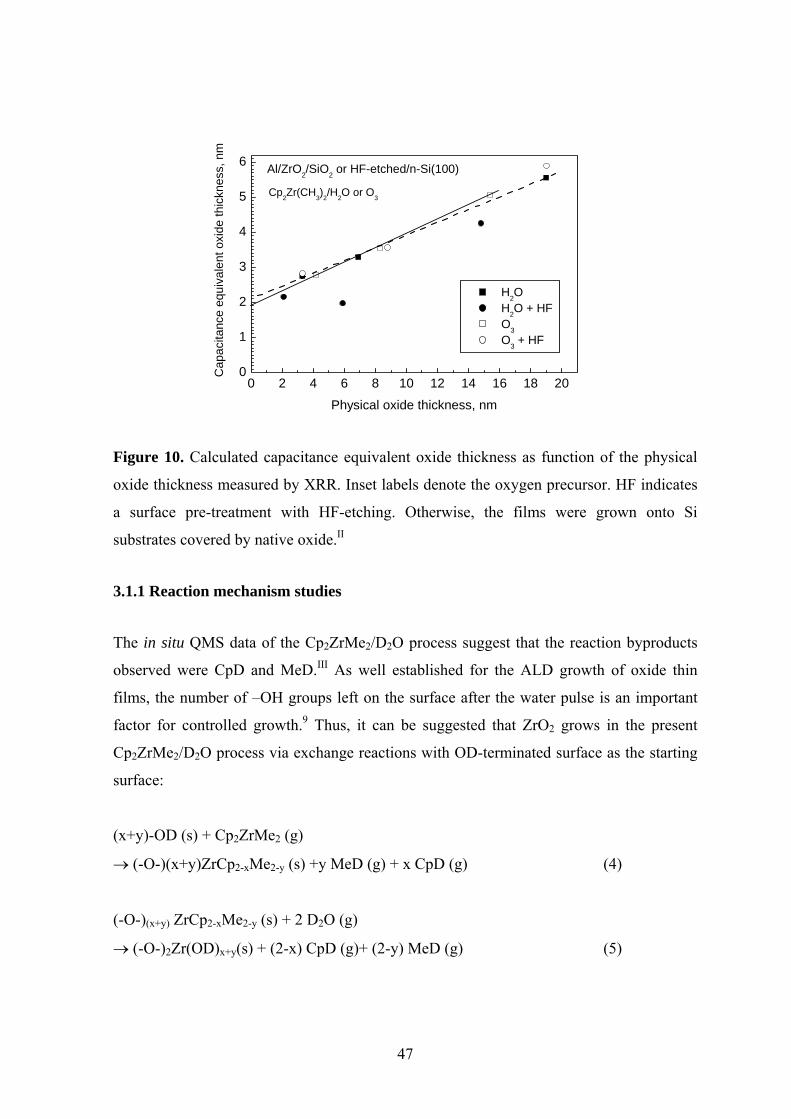
47
Figure 10. Calculated capacitance equivalent oxide thickness as function of the physical
oxide thickness measured by XRR. Inset labels denote the oxygen precursor. HF indicates
a surface pre-treatment with HF-etching. Otherwise, the films were grown onto Si
substrates covered by native oxide.II
3.1.1 Reaction mechanism studies
The in situ QMS data of the Cp2ZrMe2/D2O process suggest that the reaction byproducts
observed were CpD and MeD.III As well established for the ALD growth of oxide thin
films, the number of –OH groups left on the surface after the water pulse is an important
factor for controlled growth.9 Thus, it can be suggested that ZrO2 grows in the present
Cp2ZrMe2/D2O process via exchange reactions with OD-terminated surface as the starting
surface:
(x+y)-OD (s) + Cp2ZrMe2 (g)
→ (-O-)(x+y)ZrCp2-xMe2-y (s) +y MeD (g) + x CpD (g) (4)
(-O-)(x+y) ZrCp2-xMe2-y (s) + 2 D2O (g)
→ (-O-)2Zr(OD)x+y(s) + (2-x) CpD (g)+ (2-y) MeD (g) (5)
0 2 4 6 8 10 12 14 16 18 200
1
2
3
4
5
6
Cp2Zr(CH3)2/H2O or O3
Al/ZrO2/SiO2 or HF-etched/n-Si(100)
H2O H2O + HF O3 O3 + HF
Cap
acita
nce
equi
vale
nt o
xide
thic
knes
s, n
m
Physical oxide thickness, nm
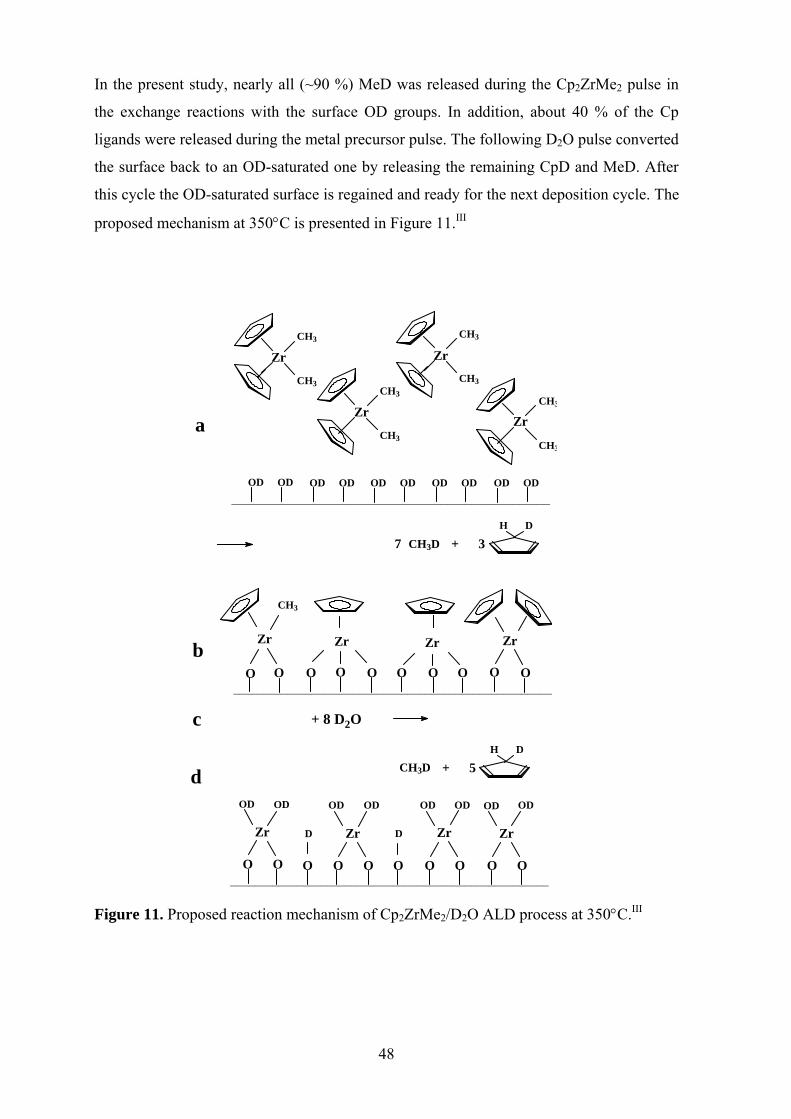
48
In the present study, nearly all (~90 %) MeD was released during the Cp2ZrMe2 pulse in
the exchange reactions with the surface OD groups. In addition, about 40 % of the Cp
ligands were released during the metal precursor pulse. The following D2O pulse converted
the surface back to an OD-saturated one by releasing the remaining CpD and MeD. After
this cycle the OD-saturated surface is regained and ready for the next deposition cycle. The
proposed mechanism at 350°C is presented in Figure 11.III
Figure 11. Proposed reaction mechanism of Cp2ZrMe2/D2O ALD process at 350°C.III
OD OD OD ODOD ODOD ODOD OD
Zr
CH3
CH3
ZrCH3
CH3
CH3
CH3
ZrCH3
CH3
Zr
a
O O O O O O O O O O
ZrZr Zr Zr
CH3
DH
37 +
+ 5H D
Zr
OOOO
OD OD
+ 8 D2O
CH3D
CH3D
D D
ODOD
O O
Zr
ODOD
O O
Zr
ODOD
O O
Zr
b
c
d
_____________________________________________________
_____________________________________________________
_____________________________________________________
49
The reaction mechanism is only weakly dependent on the deposition temperature until the
thermal decomposition of Cp2Zr(CH3)2 started which then played a role in the mechanism
at deposition temperatures exceeding 400°C. First signs of partial decomposition of the
Cp2ZrMe2 could be observed at 375°C.
3.2 HfO2 from cyclopentadienyl precursors
By applying cyclopentadienyl-type precursors for HfO2, similar growth characteristics
were observed as in the ZrO2 film deposition from the Cp2ZrMe2 precursor. The growth
rate of the polycrystalline HfO2 films by the Cp2HfMe2/H2O process was 0.42 Å/cycle at
optimized growth temperature of 350°C.IV The growth rate increased to 0.54 Å/cycle when
O3 was applied as the oxygen source.V These values can be compared to those obtained for
ZrO2: 0.43 and 0.55 Å/cycle.I,II Saturation of the growth rate was confirmed at 350°C. At
that temperature alkylamide- and alkoxide-based alternative HfO2 processes suffer from
precursor decomposition (Table 3). In the present case, promoted by the stronger oxidation
power of O3, films could be deposited with reasonable growth rates at 300°C while with
water the growth rate was low, or 0.1 Å/cycle. Above 400°C, the precursor decomposition
degraded the film uniformity over the substrate area. At 350°C, films grown by the Cl-
containing Cp-precursor, Cp2HfCl2 exhibited comparable growth rates to those provided
by Cp2HfMe2.V Generally, the growth rate of HfO2 in the current Cp-based processes is
somewhat lower than that of 0.7-1.0 Å/cycle obtained by the alkylamide-based
processes.98,105
According to the TOF-ERDA studies, films deposited from Cp2HfMe2 were stoichiometric
with low levels of C and H as impurities (Figure 12).IV,V However, due to the different
growth mechanism, and ozone being more aggressive oxidizer than water, the surface
reactions seem to be more complete with ozone resulting in lower impurity contents: viz.
below 0.1 at-% for C and H at growth temperatures of 350 and 400°C. In the films
deposited with the Cp2HfCl2, some chlorine was detected. As the Cp2HfCl2 precursor
caused Cl-contamination into the films, a drawback also recognized in the well-studied
HfCl4-based ALD-processes,89,94 further studies with the Cp2HfCl2 precursor were
discontinued. It can be concluded here that the current approach using Cp-based precursors
seems to result in films with higher purity than the other precursor combinations studied
(Table 3).

50
Figure 12. Observed Hf/O ratio at different deposition temperatures in the HfO2 films
deposited from Cp2HfMe2 and water (a) or ozone (b). In addition, the hydrogen contents
using water (c) or ozone (e) as well as the carbon content using water (d) or ozone (f) are
plotted at different deposition temperatures.V
An inhibition of growth at the early stages of the deposition on H-terminated Si similar to
that detected for the water-based processes using HfCl490 or Cp2ZrMe2,II was also observed
in the current Cp2HfMe2/H2O process.V Si-H bonds are not effectively replaced by water to
create an OH-terminated surface suitable for oxide film growth, a behavior which lead to
island nucleation, and thus, decreased film density and increased surface roughness (Figure
13).V Such a retarded growth was not observed, however, when ozone was used as an
oxygen source, for which a linear relation between thickness and number of deposition
cycles applied was observed. In addition, film roughness remained very low (Figure 13)
and the density was close to the bulk value (9-10 g/cm3). The interfacial layer thickness
between the H-terminated Si and HfO2 layer was about 0.5 nm and 1 nm for the H2O- and
O3-based processes, respectively. It should be noted that the interfacial layer obtained by
the H2O-based process is similar to that obtained by the Hf(NEtMe)4 and H2O97 ALD
process, but significantly thinner than in many other processes for HfO2, e.g. Hf(NMe2)4
and H2O,105 HfCl4 and H2O,70 or HfI4 and O2.95 The 1 nm thick interfacial layer grown
during the O3-process is similar to that obtained with the Hf(NEtMe)4/O3 process on H-
terminated Si.48 However, it should be noted that thick interfacial layer obtained by the
300 325 350 375 4000
1
2
3
4
Impu
rity
cont
ent /
at-%
Deposition temperature / oC
0.0
0.1
0.2
0.3
0.4
0.5
0.6
f)e)
a)b)
c)
d) Hf /
O ra
tio
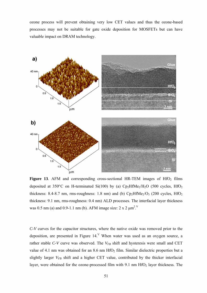
51
ozone process will prevent obtaining very low CET values and thus the ozone-based
processes may not be suitable for gate oxide deposition for MOSFETs but can have
valuable impact on DRAM technology.
Figure 13. AFM and corresponding cross-sectional HR-TEM images of HfO2 films
deposited at 350°C on H-terminated Si(100) by (a) Cp2HfMe2/H2O (500 cycles, HfO2
thickness: 8.4-8.7 nm, rms-roughness: 1.8 nm) and (b) Cp2HfMe2/O3 (200 cycles, HfO2
thickness: 9.1 nm, rms-roughness: 0.4 nm) ALD processes. The interfacial layer thickness
was 0.5 nm (a) and 0.9-1.1 nm (b). AFM image size: 2 x 2 µm2.V
C-V curves for the capacitor structures, where the native oxide was removed prior to the
deposition, are presented in Figure 14.V When water was used as an oxygen source, a
rather stable C-V curve was observed. The VFB shift and hysteresis were small and CET
value of 4.1 nm was obtained for an 8.6 nm HfO2 film. Similar dielectric properties but a
slightly larger VFB shift and a higher CET value, contributed by the thicker interfacial
layer, were obtained for the ozone-processed film with 9.1 nm HfO2 layer thickness. The
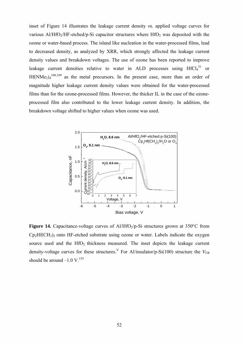
52
inset of Figure 14 illustrates the leakage current density vs. applied voltage curves for
various Al/HfO2/HF-etched/p-Si capacitor structures where HfO2 was deposited with the
ozone or water-based process. The island like nucleation in the water-processed films, lead
to decreased density, as analyzed by XRR, which strongly affected the leakage current
density values and breakdown voltages. The use of ozone has been reported to improve
leakage current densities relative to water in ALD processes using HfCl451 or
Hf(NMe2)4108,109 as the metal precursors. In the present case, more than an order of
magnitude higher leakage current density values were obtained for the water-processed
films than for the ozone-processed films. However, the thicker IL in the case of the ozone-
processed film also contributed to the lower leakage current density. In addition, the
breakdown voltage shifted to higher values when ozone was used.
Figure 14. Capacitance-voltage curves of Al/HfO2/p-Si structures grown at 350°C from
Cp2Hf(CH3)2 onto HF-etched substrate using ozone or water. Labels indicate the oxygen
source used and the HfO2 thickness measured. The inset depicts the leakage current
density-voltage curves for these structures.V For Al/insulator/p-Si(100) structure the VFB
should be around –1.0 V.155
-6 -5 -4 -3 -2 -1 0 1
0.0
0.5
1.0
1.5
2.0
0 1 2 3 4 5 6 710-11
1x10-101x10-91x10-81x10-71x10-61x10-51x10-41x10-31x10-21x10-11x1001x101
O3, 9.1 nm
H2O, 8.6 nm
Cur
rent
den
sity
, A/c
m2
Voltage, V
Al/HfO2/HF-etched p-Si(100)Cp2Hf(CH3)2/H2O or O3
H2O, 8.6 nm
O3, 9.1 nm
Cap
acita
nce,
nF
Bias voltage, V

53
3.3 Rare earth oxide thin films from cyclopentadienyl precursors
3.3.1 Y2O3
ALD-type growth of Y2O3 was achieved with two precursor combinations, applying either
Cp3Y/H2O or (CpMe)3Y/H2O processes.VI ALD-type growth was confirmed in both
processes at 250°C and 300°C. The growth rate obtained by the (CpMe)3Y/H2O process
was 1.2-1.3 Å/cycle in a wide temperature range, with the ALD window regime being 200-
400°C. This growth rate is about six times higher than that obtained by the conventional
Y(thd)3/O3 process.135 The growth rate was further increased to 1.6 Å/cycle by using the
Cp3Y/H2O process at 300°C, but an ALD window could not be detected with this precursor
system. Generally, the Y2O3 films obtained with both Cp-based processes were
stoichiometric and contained less than 0.5 at-% of carbon as an impurity. Hydrogen
content was dependent on the deposition temperature being lowest at 0.9 at-% for the films
deposited with the (CpMe)3Y/H2O process at 400°C. Notably, the Y2O3 film crystallinity
was strongly dependent on the precursor combination and the deposition temperature
applied (Figure 15). The Cp3Y as precursor yielded a significantly higher growth rate than
(CpMe)3Y and in addition, the crystallinity of the Y2O3 films with the Cp3Y/H2O process
was more pronounced, exhibiting (222) as the preferred orientation in the entire deposition
temperature range of 175 to 400°C studied. In the case of the (CpMe)3Y precursor, more
thermal energy was needed to achieve the (222) as the dominant orientation; the change
from (400) to (222) as the preferred orientation occurs only around 400°C. When
comparing the current Cp-based processesVI to the Y(thd)3/O3 ALD process,135 the
crystallinity was strongly enhanced (Figure 15). The increase in crystallinity as deposition
temperature is increased also correlated with the surface morphology; both Cp-based
processes the smoothest films were deposited at temperatures of 250°C or below.
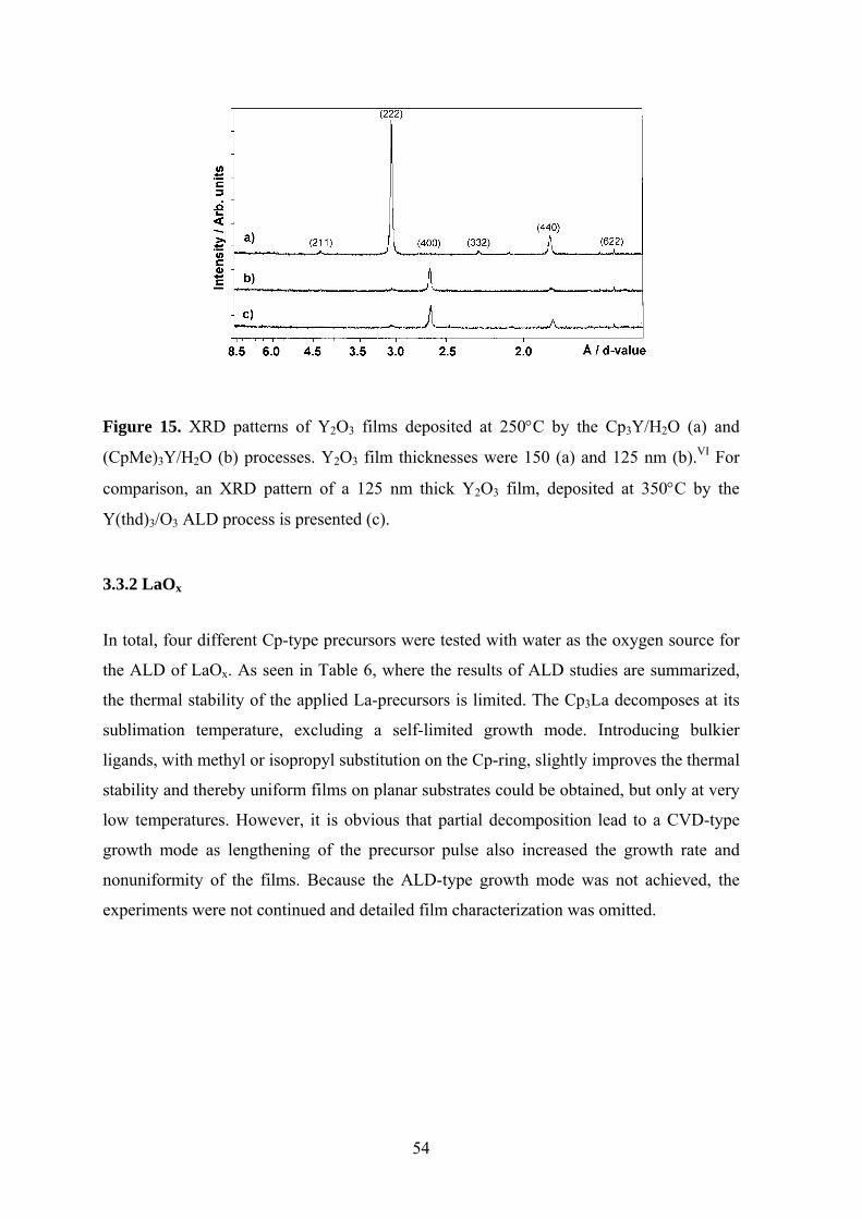
54
Figure 15. XRD patterns of Y2O3 films deposited at 250°C by the Cp3Y/H2O (a) and
(CpMe)3Y/H2O (b) processes. Y2O3 film thicknesses were 150 (a) and 125 nm (b).VI For
comparison, an XRD pattern of a 125 nm thick Y2O3 film, deposited at 350°C by the
Y(thd)3/O3 ALD process is presented (c).
3.3.2 LaOx
In total, four different Cp-type precursors were tested with water as the oxygen source for
the ALD of LaOx. As seen in Table 6, where the results of ALD studies are summarized,
the thermal stability of the applied La-precursors is limited. The Cp3La decomposes at its
sublimation temperature, excluding a self-limited growth mode. Introducing bulkier
ligands, with methyl or isopropyl substitution on the Cp-ring, slightly improves the thermal
stability and thereby uniform films on planar substrates could be obtained, but only at very
low temperatures. However, it is obvious that partial decomposition lead to a CVD-type
growth mode as lengthening of the precursor pulse also increased the growth rate and
nonuniformity of the films. Because the ALD-type growth mode was not achieved, the
experiments were not continued and detailed film characterization was omitted.
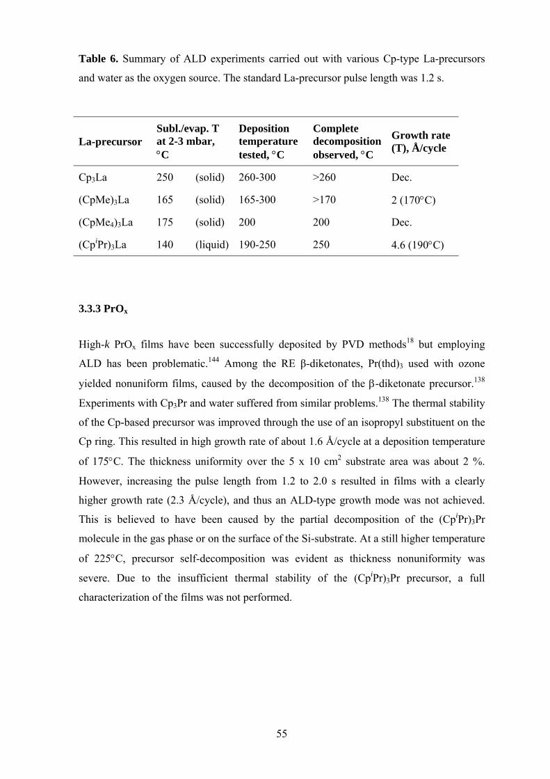
55
Table 6. Summary of ALD experiments carried out with various Cp-type La-precursors
and water as the oxygen source. The standard La-precursor pulse length was 1.2 s.
3.3.3 PrOx
High-k PrOx films have been successfully deposited by PVD methods18 but employing
ALD has been problematic.144 Among the RE β-diketonates, Pr(thd)3 used with ozone
yielded nonuniform films, caused by the decomposition of the β-diketonate precursor.138
Experiments with Cp3Pr and water suffered from similar problems.138 The thermal stability
of the Cp-based precursor was improved through the use of an isopropyl substituent on the
Cp ring. This resulted in high growth rate of about 1.6 Å/cycle at a deposition temperature
of 175°C. The thickness uniformity over the 5 x 10 cm2 substrate area was about 2 %.
However, increasing the pulse length from 1.2 to 2.0 s resulted in films with a clearly
higher growth rate (2.3 Å/cycle), and thus an ALD-type growth mode was not achieved.
This is believed to have been caused by the partial decomposition of the (CpiPr)3Pr
molecule in the gas phase or on the surface of the Si-substrate. At a still higher temperature
of 225°C, precursor self-decomposition was evident as thickness nonuniformity was
severe. Due to the insufficient thermal stability of the (CpiPr)3Pr precursor, a full
characterization of the films was not performed.
La-precursor Subl./evap. T at 2-3 mbar, °C
Deposition temperature tested, °C
Complete decomposition observed, °C
Growth rate (T), Å/cycle
Cp3La 250 (solid) 260-300 >260 Dec.
(CpMe)3La 165 (solid) 165-300 >170 2 (170°C)
(CpMe4)3La 175 (solid) 200 200 Dec.
(CpiPr)3La 140 (liquid) 190-250 250 4.6 (190°C)
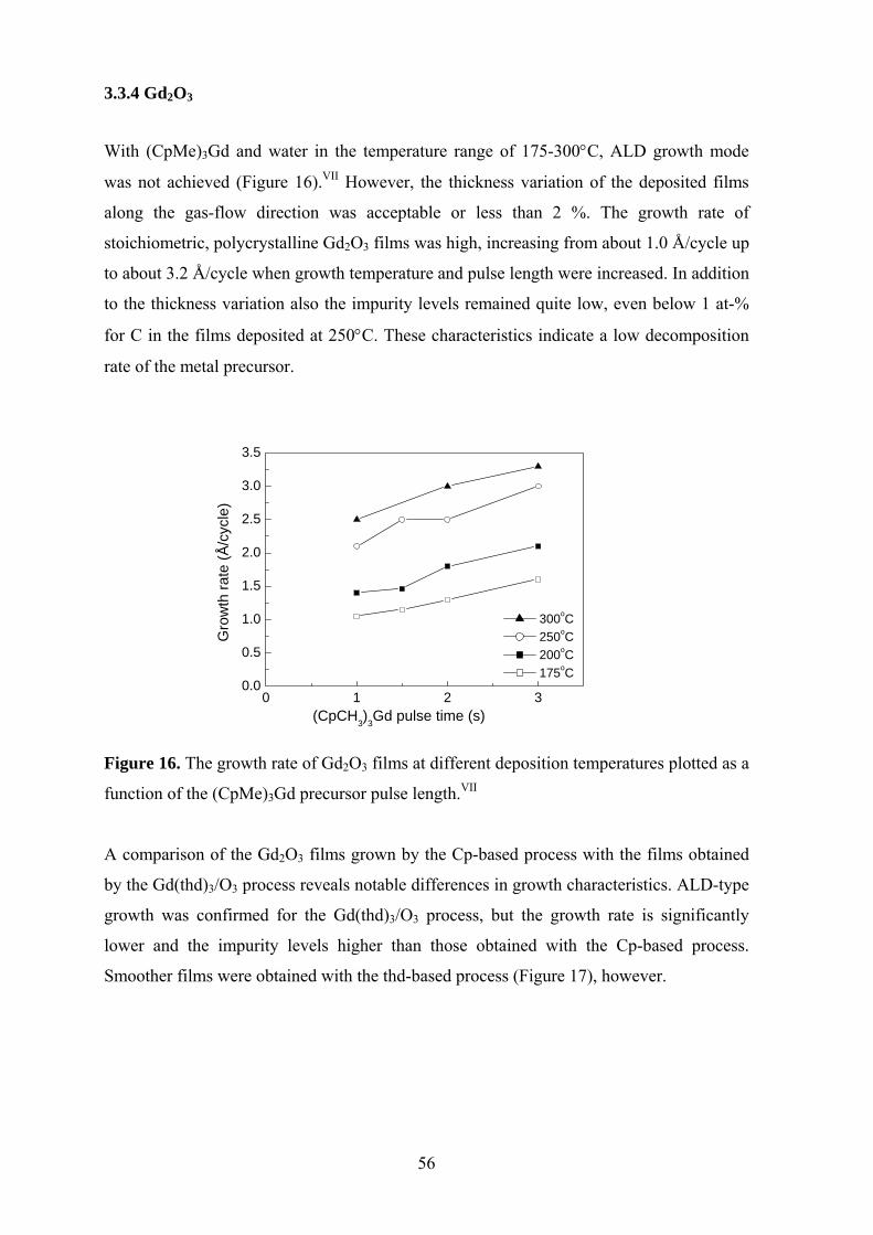
56
3.3.4 Gd2O3
With (CpMe)3Gd and water in the temperature range of 175-300°C, ALD growth mode
was not achieved (Figure 16).VII However, the thickness variation of the deposited films
along the gas-flow direction was acceptable or less than 2 %. The growth rate of
stoichiometric, polycrystalline Gd2O3 films was high, increasing from about 1.0 Å/cycle up
to about 3.2 Å/cycle when growth temperature and pulse length were increased. In addition
to the thickness variation also the impurity levels remained quite low, even below 1 at-%
for C in the films deposited at 250°C. These characteristics indicate a low decomposition
rate of the metal precursor.
Figure 16. The growth rate of Gd2O3 films at different deposition temperatures plotted as a
function of the (CpMe)3Gd precursor pulse length.VII
A comparison of the Gd2O3 films grown by the Cp-based process with the films obtained
by the Gd(thd)3/O3 process reveals notable differences in growth characteristics. ALD-type
growth was confirmed for the Gd(thd)3/O3 process, but the growth rate is significantly
lower and the impurity levels higher than those obtained with the Cp-based process.
Smoother films were obtained with the thd-based process (Figure 17), however.
0 1 2 30.0
0.5
1.0
1.5
2.0
2.5
3.0
3.5
300oC 250oC 200oC 175oC
Gro
wth
rate
(Å/c
ycle
)
(CpCH3)3Gd pulse time (s)

57
Figure 17. AFM images for 100 nm thick Gd2O3 films deposited at 250 °C by the
Gd(thd)3/O3 (a) and (CpCH3)3Gd/H2O (b) processes. The rms-roughness values were 1.2
(a) and 2.5 nm (b), respectively.VII
While true ALD-type growth was not achieved by the (CpMe)3Gd/H2O process, the more
bulky (CpMe4)3Gd precursor was tested in an attempt to overcome the partial
decomposition problem. However, already at the deposition temperature of 250°C signs of
precursor decomposition could be detected, and consequently the thickness uniformity was
poor. Increasing the pulse length of the (CpMe4)3Gd precursor from 1.2 s to 2.0 s enhanced
the growth rate from 1.2 to 1.8 Å/cycle, which confirmed the absence of ALD-type growth
mode.
3.3.5 Er2O3
A constant and high growth rate of 1.5 Å/cycle was achieved by the ALD process of Er2O3
employing (CpMe)3Er and H2O as precursors at 250-350°C.VIII This well-behaving process
yielded films with good uniformity and high purity. The impurity levels were lower than in
the erbia films deposited by the thd- or amidinate-based processes.42,136 The ALD-type
growth mode was confirmed at 250 and 300°C where for complete saturation a pulse
length of 1.5 s was required. The decomposition of the metal precursor affected the film
growth behaviour at temperatures above 350°C. The rms-roughness increased as the
deposition temperature was increased. The increase in crystallinity and, at temperatures
above 350°C, the partial decomposition of the precursor is believed to cause the observed
increase in roughness. Because of its thermal stability and reactivity, this Cp-precursor

58
offers clear advantages for Er2O3 film growth over the β-diketonate or amidinate-type
erbium precursors.42,136
3.3.6 Rare earth scandates
Amorphous, high-permittivity rare earth scandates, namely YScO3, GdScO3 and ErScO3,
can be deposited by ALD using either Cp-type precursors and water or β-diketonate-type
precursor and ozone as precursors.IX,156 Considering that the ALD processes of the binary
RE oxides are well-established and function in a self-controlled manner, RE scandates
having a range of stoichiometries were straightforwardly deposited using different pulsing
ratios in the RE processes, e.g. with pulsing ratio of 6:5 ((CpMe)3Y + H2O: Cp3Sc + H2O),
a stoichiometry of Y1.03Sc0.96O3.01 was achieved.IX By applying the same pulsing ratio but
using (CpMe)3Er instead, the Er1.02Sc0.98O3 composition was obtained. As expected,
considerably higher growth rates were obtained with the Cp-based processes than with the
β-diketonate-based processes. All the films were amorphous as deposited and
crystallization upon annealing was dependent on the precursors used. The YScO3 films
deposited by the thd-precursors and ozone remained amorphous even after rapid thermal
annealing at 800°C under N2 ambient. In contrast, the YScO3 films from the Cp-precursors
became crystalline after RTA treatment at 800°C. It should be noted that the YScO3 films
crystallized as a solid solution of Y2O3 and Sc2O3 rather than forming a crystalline YScO3
phase.IX In the case of GdScO3 grown from thd-precursors and ozone, the Gd-scandate
phase was observed to form after RTA treatment at 1000°C.156 Stoichiometric GdScO3 was
deposited with a pulsing ratio of 5 : 11 (Gd(thd)3 + O3: Sc(thd)3 + O3).
3.3.7 Dielectric properties of the RE oxide films
Due to the thermal instability of the La- and Pr-precursors studied, thin La- or Pr-oxide
layers for electrical measurements were not deposited. However, Al/RE oxide/native
SiO2/p- or n-Si/Al capacitor structures, where RE oxide layer was Y2O3, Gd2O3, Er2O3,
YScO3, ErScO3, or GdScO3, were measured for C-V and I-V characteristics. High positive
fixed charges were detected in the Y2O3 films grown with both Cp-precursors.VI In
addition, breakdown fields were rather low, likely caused by high crystallinity of the
relatively thick films where the grain boundaries offer pathways for leakage current.
Effective permittivity of the films was about 10, which is slightly lower than that obtained
59
with the Y[iPramdiPr]/H2O ALD process.146 It should be noted that annealing was not
performed for these Y2O3 films,VI while in the study by de Rouffignac et al.146 very long
deposition times (>12 hrs for 50 nm film) were used, thus actually having an annealing
effect during the deposition. Despite the fact that a true ALD-type growth mode was not
achieved for the (CpMe)3Gd/H2O process, the Gd2O3 films showed well-behaved C-V
curves.VII The permittivity was in the range of 13-14, which is considerably higher than the
values obtained for the Gd2O3 films grown by the thd-based process. However, flatband
voltage shift, also reported for other RE oxides,24 was significant. Similar to the case of
Y2O3, leakage current was affected by the polycrystalline nature of the films.VI,VII Er2O3
films seemed to possess a reduced amount of fixed charge and their hysteresis was
negligible.VIII The effective permittivity of a 12.5 nm Er2O3 film and native SiO2 stack was
about 10, but if the native SiO2 interfacial layer is not taken into account, a value of 14 can
be calculated for the erbia film.
The rare earth scandates, because of their amorphous structure seem to be better
alternatives for gate dielectric applications than the more often studied RE binary
oxides.IX,156 Figure 18 depicts the C-V curves for capacitor structures where the insulator,
YScO3 or GdScO3, is deposited by the thd-precursors and ozone. An effective permittivity
of 14-15 could be calculated which is considerably higher than that (9-10) obtained for
Y2O3, Gd2O3 and Sc2O3 binary oxides deposited from the thd-precursors. When Cp-
precursors were applied for the deposition of YScO3 and ErScO3 the effective permittivity
was high but considerable hysteresis was detected, indicating positively charged ions in the
films. Because of the amorphous nature of the films, leakage current density remained low
(e.g. 1 x 10⁻⁸ A cm-2 at V=VFB - 1 V for 40 nm YScO3 film). Upon annealing at 1000°C, the
crystallization as a solid solution of binary oxides leads to lower permittivity values as well
as increased leakage current density. This pioneering study on ALD of RE scandates
appears to offer an interesting starting point for further investigations aiming at high-k
applications.

60
Figure 18. Capacitance-voltage curves of Al/YScO3 or GdScO3/native SiO2/p-Si(100)
capacitor structures with YScO3 and GdScO3 films deposited from Y(thd)3 or Gd(thd)3 and
Sc(thd)3 with O3 as the oxygen source. Labels indicate the insulator thickness and effective
permittivity values.IX,156 For Al/insulator/p-Si(100) structure the VFB should be around –1.0
V.155
3.3.8 Rare earth precursor selection
In the ALD of RE oxide thin films from Cp-type precursors, the limited thermal stability of
the precursor seems to be the major problem. The correlation of the rare earth ionic radius
and the ligand size on the thermal stability was previously introduced.46 This prediction
can now be complemented by the present results (Table 7). It clearly seems that
introducing the bulkier Cp-ligands, e.g. with methyl or isopropyl substitution, thermal
stability can be increased, but for large ions such as Pr3+ and La3+, achievement of ALD-
type growth mode at reasonable temperatures still remains a very challenging task.
-6 -5 -4 -3 -2 -1 0 1 2 3 4 5
0.0
0.1
0.2
0.3
0.4
0.5
0.6
0.7
0.8
0.9
YScO3, 37 nm, keff=15 annealed at 800oC
YScO3, 39.4 nm, keff=14.2
GdScO3, 40.6 nm, keff=13.6
Bias voltage, V
Cap
acita
nce,
nF
Al/REScO3/SiO2/p-Si(100)/Al f=500 kHz Y(thd)3, Gd(thd)3, Sc(thd)3, O3

61
Table 7. The suitability of different Cp-compounds applied/tested in the ALD processes
for the growth of selected RE oxide films. Mixed-ligand compounds which contain Cp and
some other ligands are omitted.
Ligand Rare
earth
Ionic
(+III)
radius, Å Cp CpMe CpiPr CpMe4
Sc 0.75 Suitable
Er 0.89 Suitable
Y 0.90 Suitable Suitable
Gd 0.94 Partial dec. Partial dec.
Pr 0.99 Not suitable Partial dec. Not suitable
Ce 1.02 Not suitable
La 1.03 Not suitable Partial dec. Partial dec. Not suitable
62
4. CONCLUSIONS
The suitability of cyclopentadienyl-type precursors in ALD has earlier been established for
noble metals,157 alkaline-earth metal containing oxides158,159 and sulfides160 as well as for
scandium oxide133 deposition. For high-k oxide deposition the possibilities to modify the
precursor chemistry are extensive. For the controlled ALD of ZrO2 and HfO2, the methyl-
substituted Cp-type precursors, Cp2ZrMe2 and Cp2HfMe2, clearly have some advantageous
features: The obtained film purity is high and the suitable deposition temperature is higher
(up to 375-400°C) than in many other alternative halide-free processes. However, when
water is used as the oxygen source the observed retarded growth on H-terminated Si can be
considered as a drawback. With ozone, on the other hand, the roughness, impurity content,
and leakage current density can be decreased. In general, the electrical characterization
showed promising dielectric properties for high-k applications. The growth of ZrO2 from
Cp2ZrMe2 and deuterated water was studied in situ by QMS revealing that nearly all the
methyl ligands and less than half of the Cp-ligands were released during the metal
precursor pulse. The remaining ligands were released during the subsequent surface
reaction with deuterated water, leaving the surface OD-terminated, and thus ready for the
next cycle. The in situ studies showed that the decomposition onset temperature for
Cp2ZrMe2 precursor was around 375°C.
A number of Cp-type precursors were applied for the deposition of RE oxides. Cp3Y,
(CpMe)3Y, and (CpMe)3Er were found to have sufficient thermal stability in water-based
processes for self-limiting, ALD-type growth of the corresponding RE oxide thin films.
The growth rate was about six times higher than with the conventional β-diketonate
precursors reacting with ozone.24,135,VI,VIII High purity, better stoichiometry as well as
higher permittivity of the resulting oxide films can also be counted among the benefits of
the current Cp-precursor approach. However, the thermal stability of the Cp-compounds is
limited especially for larger RE ions, such as Gd, Pr and La. Stability can be improved by
introducing bulkier ligands, such as isopropyl substitution, but in many cases partial
decomposition destroys the preferred ALD-type growth mode resulting in films with poor
uniformity. However, with the (CpMe)3Gd/H2O process, high quality films on planar
surfaces with promising dielectric properties were obtained despite the fact that partial
decomposition prevented the surface-saturative growth mode.

63
Finally, ternary RE scandates, YScO3, GdScO3, and ErScO3 were successfully grown by
ALD as solid solutions of the individual binary oxides. These scandates were amorphous
as-deposited and, depending on the precursor combination used, RTA at 800 or 1000°C
was required for their crystallization. In addition to the amorphous structure, clearly
beneficial to minimize leakage current, the effective permittivity (15-16) was considerably
higher than that of the binary oxides (10).
The results obtained in this work show that Cp-type compounds are suitable for high-k
depositions by ALD. Precursor chemistry is the key factor in the development of novel
ALD processes and there Cp-type precursors offer a viable route to achieve high-quality
oxide films not previously successfully processed by ALD. In addition, Cp-type precursors
together with a proper oxygen source selection, can improve the film properties of
important materials, such as ZrO2 or HfO2.

64
5. REFERENCES
1. Suntola, T. and Antson, J., US Patent 4 058 430 (1977).
2. Leskelä, M. and Ritala, M., Angew. Chem. Int. Ed. 42 (2003) 5548.
3. International Technology Roadmap for Semiconductors, http://public.itrs.net/,
5.1.2006.
4. Hand, A. Semicond. Int. 26(5) (2003) 46.
5. Wilk, G.D., Wallace R.M., and Anthony, J.M., J. Appl. Phys. 89 (2001) 5243.
6. Misra, D., Iwai, H., and Wong, H., Electrochem. Soc. Interface 14(2) (2005) 30.
7. Robertson, J., Rep. Prog. Phys. 69 (2006) 327.
8. Houssa M. and Heyns, M.M., in High-k Gate Dielectrics, ed. Houssa, M., Institute of
Physics Publishing, Bristol 2004, pp. 3-13.
9. Ritala M. and Leskelä, M., in Handbook of Thin Film Materials, ed. Nalwa, H.S.,
Academic Press, New York 2002, vol. 1, pp. 103-159.
10. Musgrave, C. and Gordon, R.G., Future Fab. Int. 18 (2005) 126.
11. Lysaght, P.S., Foran, B., Bersuker, G., Chen, P.J., Murto, R.W., and Huff, H.R.,
Appl. Phys. Lett. 82 (2003) 1266.
12. Niinistö, L., Päiväsaari, J., Niinistö, J., Putkonen M., and Nieminen, M., Phys. Stat.
Sol. A 201 (2004) 1443.
13. Moore, G.E., Electronics, 38 (1965) 114.
14. http://www.intel.com, 4.1.2006.
15. Hubbard, K.J. and Schlom, D.G., J. Mater. Res. 11 (1996) 2757.
16. Schlom, D.G. and Haeni, J.H., MRS Bull. 27 (2002) 198.
17. Robertson, J., Solid-State Electron. 49 (2005) 283.
18. Osten, H.J., Bugiel, E., Kirfel, O., Czernohorsky, M., and Fissel, A., J. Cryst. Growth
278 (2005) 18.
19. Ribes, G., Mitard, J., Denais, M., Bruyere, S., Monsieur, F., Parthasarathy, C.,
Vincent, E., and Ghibaudo, G., IEEE Trans. Device Mater. Reliab. 5 (2005) 5.
20. Guha, S., Gusev, E., Copel, M., Ragnarsson, L.-Å., and Buchanan, MRS Bull. 27
(2002) 226.
21. Heeg, T., Wagner, M., Schubert, J., Buchal, C., Boese, M., Luysberg, M., Cicerrella
E., and Freeouf, J.L., Microelectron. Eng. 80 (2005) 150.
22. Quevedo-Lopez, M.A., Krishnan, S.A., Kirsch, P.D., Pant, G., Gnade, B.E., and
65
Wallace, R.M., Appl. Phys. Lett. 87 (2005) 262902.
23. Osten, H.J., Bugiel, E., and Fissel, A., Solid-State Electr. 47 (2003) 2161.
24. Päiväsaari, J., Putkonen, M., and Niinistö, L., Thin Solid Films 472 (2005) 275.
25. Gerritsen, E., Emonet, N., Caillat, C., Jourdan, N., Piazza, M., Fraboulet, D., Boeck,
B., Berthelot, A., Smith, S., and Mazoyer, P., Solid-State Electron. 49 (2005) 1767.
26. Pakkala, A., AVS 4th International Conference on Atomic Layer Deposition, Helsinki,
Finland, 2004, Extended Abstracts on CD-ROM.
27. Niinistö, L., Ritala, M., and Leskelä, M., Mater. Sci. Eng. B 41 (1996) 23.
28. Leskelä, M. and Ritala, M., Thin Solid Films 409 (2002) 138.
29. Niinistö, L., Curr. Opin. Solid State & Mater. Sci. 3 (1998) 147.
30. Puurunen, R.L., J. Appl. Phys. 97 (2005) 121301.
31. Suntola, T., Appl. Surf. Sci. 100/101 (1996) 391.
32. Elers, K.-E., Blomberg, T., Peussa, M., Aitchison, B., Haukka, S., and Marcus, S.,
Chem. Vap. Deposition 12 (2006) 13.
33. Conley, Jr., J.F., Ono, Y., Zhuang, W., Tweet, D.J., Gao, W., Mohammed S.K., and
Solanki, R., Electrochem. Solid-State Lett. 5 (2002) C57.
34. Matero, R., Atomic Layer Deposition of Oxide Film–Growth Characterisation and
Reaction Mechanism Studies, Doctoral dissertation, University of Helsinki, Helsinki
2005, 61 p.
35. Jones, A.C., Aspinall, H.C., Chalker, P.R., Potter, R.J., Kukli, K., Rahtu, A., Ritala,
M., and Leskelä, M., J. Mater. Chem. 14 (2004) 3101.
36. Jones, A.C., Aspinall, H.C., Chalker, P.R., Potter, R.J., Kukli, K., Rahtu, A., Ritala,
M., and Leskelä M., Mater. Sci. Eng. B 118 (2005) 97.
37. Tiitta, M. and Niinistö, L., Chem. Vap. Deposition 3 (1997) 167.
38. CVD on Nonmetals, ed. Rees, Jr., W.S., VCH Verlagsgesellschaft GmbH, Weinheim
1996, 424 p.
39. Binnemans, K., in Handbook on the Physics and Chemistry of Rare Earths, eds.
Gschneider, Jr., K.A., Bünzli, J.-C.G., and Pecharsky, V.K., Elsevier, Amsterdam
2005, Vol. 35, pp. 238-241.
40. Putkonen, M., Development of Low-temperature Deposition Processes by Atomic
Layer Epitaxy for Binary and Ternary Oxide Thin Films, Doctoral dissertation,
Helsinki University of Technology, Helsinki 2002, 69 p.
41. Lim, B.S., Rahtu, A., and Gordon, R.G., Nature Mater. 2 (2003) 729.

66
42. Päiväsaari, J., Dezelah, C.L., Back, D., El-Kaderi, H.M., Heeg, M.J., Putkonen, M.,
Niinistö, L., and Winter, C.H., J. Mater. Chem. 15 (2005) 4224.
43. Lujala, V., Skarp, J., Tammenmaa, M., and Suntola, T., Appl. Surf. Sci. 82-83 (1994)
34.
44. Kealy, T.J. and Pauson, P.L., Nature 168 (1951) 1039.
45. Miller, S.A., Tebboth, J.A., and Tremaine, J.F., J. Chem. Soc. (1952) 632.
46. Putkonen, M. and Niinistö, L., Top. Organomet. Chem. 9 (2005) 125.
47. Long, N.J., Metallocenes: An Introduction to Sandwich Compounds, Blackwell
Science Ltd., Oxford 1998, 285 p.
48. Gusev, E.P., Cartier, E., Buchanan, D.A., Gribelyuk, M., Copel, M., Okorn-Schmidt,
H., and D’Emic, C., Microelectron. Eng. 59 (2001) 341.
49. Park, C.S., Moumen, B.M., Sim, J.H., Barnett, J., Lee, B.H., and Bersuker, G., Appl.
Phys. Lett. 87 (2005) 253510.
50. Ha, S.-C., Choi, E., Kim, S.-H., and Roh, J.S., Thin Solid Films 476 (2005) 252.
51. Park, H.B., Cho, M., Park, J., Lee, S.W., Hwang, C.S., Kim, J.-P., Lee, J.-H., Lee,
N.-I., Lee H.-K., and Oh, S.-J., J. Appl. Phys. 94 (2003) 3641.
52. Copel, M., Gribelyuk M., and Gusev, E., Appl. Phys. Lett. 76 (2000) 436.
53. Green, M.L., Allen, A.J., Li, X., Wang, J., Ilavsky, J., Delabie, A., Puurunen, R.L.,
and Brijs, B., Appl. Phys. Lett. 88 (2006) 032907.
54. Nieminen, M., Deposition of Binary and Ternary Oxide Thin Films of Trivalent
Metals by Atomic Layer Epitaxy, Doctoral dissertation, Helsinki University of
Technology, Helsinki 2001, 57 p.
55. Ritala, M. and Leskelä, M. Appl. Surf. Sci. 1994, 75, 333.
56. Perkins, C.M., Triplett, B.B., McIntyre, P.C., Saraswat, K.C., Haukka, S., and
Tuominen, M., Appl. Phys. Lett. 78 (2001) 2357.
57. Kukli, K., Ritala, M., Aarik, J., Uustare T., and Leskelä, M. J. Appl. Phys. 92 (2002)
1833.
58. Aarik, J., Aidla, A., Mändar, H., Uustare T., and Sammelselg, V., Thin Solid Films
408 (2002) 97.
59. Sammelselg, V., Rauhala, E., Arstila, K., Zakharov, A., Aarik, J., Kikas, A., Karlis,
J., Tarre, A., Seppälä, A., Asari, J., and Martinson, I., Mikrochim. Acta 139 (2002)
165.
60. Nohira, H., Tsai, W., Besling, W., Young, E., Petry, J., Conard, T., Vandervorst, W.,
67
De Gendt, S., Heyns, M., Maes, J., and Tuominen, M., J. Non-Cryst. Solids 303
(2002) 83.
61. Ferrari, S., Scarel, G., Wiernier, C., and Fanciulli, M., J. Appl. Phys. 92 (2002) 7675.
62. Zhao, C., Roebben, G., Bender, H., Young, E., Haukka, S., Houssa, M., Naili, M., De
Gendt, S., Heyns, M., and Van Der Biest, O., Microelectr. Reliability 41 (2001) 995.
63. Besling, W.F.A., Young, E., Conard, T., Zhao, C., Carter, R., Vandervorst, W.,
Caymax, M., De Gendt, S., Heyns, M., Maes, J., Tuominen, M., and Haukka., S., J.
Non-Cryst. Sol. 303 (2002) 123.
64. Rahtu, A. and Ritala, M., J. Mater. Chem. 12 (2002) 1484.
65. Conard, T., Vandervorst, W., Petry, J., Zhao, C., Besling, W., Nohira, H., and
Richard, O., Appl. Surf. Sci. 203-204 (2003) 400.
66. Kukli, K., Forsgren, K., Ritala, M., Leskelä, M., Aarik, J., and Hårsta, A., J.
Electrochem. Soc. 148 (2001) F227.
67. Kukli, K., Forsgren K., Aarik, J., Uustare, T., Aidla, A., Niskanen, A., Ritala M.,
Leskelä, M., and Hårsta, A., J. Cryst. Growth 231 (2001) 262.
68. Kukli, K., Ritala, M., Uustare, T., Aarik, J., Forsgren, K., Sajavaara, T., Leskelä, M.,
and Hårsta, A., Thin Solid Films 410 (2002) 53.
69. Forsgren, K., Westlinder, J., Lu, J., Olsson, J., and Hårsta, A., Chem. Vap.
Deposition 8 (2002) 105.
70. Kukli, K., Ritala, M., Leskelä, M., Sajavaara, T., Keinonen, J., Gilmer, D.C., Hegde,
R., Rai, R., and Prabhu, L., J. Mater. Sci.; Mater. Electron. 14 (2003) 361.
71. Hausmann, D.M., Kim, E., Becker J., and Gordon, R.G., Chem. Mater. 14 (2002)
4350.
72. Kim, Y., Koo, J., Han, J., Choi, S., Jeon, H., and Park, C.-G., J. Appl. Phys. 92
(2002) 5443.
73. Yun, S.J., Lim, J.W., and Lee, J.-H., Electrochem. Solid-State Lett. 7 (2004) F81.
74. Yun, S.J., Lim, J.W., and Lee, J.-H., Electrochem. Solid-State Lett. 8 (2005) F47.
75. Kim, J.Y., Kim, S.H., Seo, H., Kim, J.-H., and Jeon, H., Electrochem. Solid-State
Lett. 8 (2005) G82.
76. Hausmann, D.M. and Gordon, R.G., J. Cryst. Growth 249 (2003) 251.
77. Nam, W.-H. and Rhee, S.-W., Chem. Vap. Deposition 10 (2004) 201.
78. Kukli, K., Ritala, M., and Leskelä, M., Chem. Vap. Deposition 6 (2000) 297.
79. Jeong, D., Lee, J., and Kim, J., Integr. Ferroelect. 67 (2004) 41.

68
80. Nakajima, A., Kidera, T., Ishii, H., and Yokoyama, S., Appl. Phys. Lett. 81 (2002)
2824.
81. Lao, S.X., Martin, R.M., and Chang, J.P., J. Vac. Sci. Technol. A 23 (2005) 488.
82. Endo, K. and Tatsumi, T., Jpn. J. Appl. Phys. 42 (2003) L685.
83. Matero, R., Ritala, M., Leskelä, M., Sajavaara, T., Jones, A.C., and Roberts, J.L.,
Chem. Mater. 16 (2004) 5630.
84. Matero, R., Ritala, M., Leskelä, M., Jones, A.C., Williams, P.A., Bickley, J.F.,
Steiner, A., Leedham, T.J., and Davies, H.O., J. Non-Cryst. Solids 303 (2002) 24.
85. Putkonen, M. and Niinistö, L., J. Mater. Chem. 11 (2001) 3141.
86. Yoshii, N., Takahashi, N., Nakamura, T., and Yoshioka, M., Electrochem. Solid-
State Lett. 5 (2005) C85.
87. Kattelus, H., Ylilammi, M., Salmi, J., Aho, T.R., Nykänen, E, and Suni, I., Mat. Res.
Soc. Symp. Proc., 284 (1993) 511.
88. Ritala, M., Leskelä, M., Niinistö, L. Prohaska, T., Friedbacher, G., and Grasserbauer,
M., Thin Solid Films, 250 (1994) 72.
89. Ganem, J.-J., Trimaille, I., Vickridge, I.C., Blin, D., and Martin, F., Nucl. Instrum.
Meth. Phys. Res. B, 219-220 (2004) 856.
90. Gusev, E.P., Cabral, Jr., C., Copel, M., D’Emic, C., and Gribelyuk, M., Microel.
Eng. 69 (2003) 145.
91. Aarik, J., Aidla, A., Kiisler, A.-A., Uustare T., and Sammelselg, V., Thin Solid Films
340 (1999) 110.
92. Aarik, J., Aidla, A., Mändar, H., Sammelselg V., and Uustare, T. J. Cryst. Growth
220 (2000) 105.
93. Triyoso, D.H., Hegde, P.I., White, Jr., B.E., and Tobin, P.J., J. Appl. Phys. 97 (2005)
124107.
94. Kukli, K., Ritala, M., Sajavaara, T., Keinonen J., and Leskelä, M., Thin Solid Films
416 (2002) 72.
95. Aarik, J., Sundqvist, J., Aidla, A., Lu, J., Sajavaara, T., Kukli, K., and Hårsta, A.,
Thin Solid Films 418 (2002) 69.
96. Kukli, K., Ritala, M., Sundqvist, J., Aarik, J., Lu, J., Sajavaara, T., Leskelä, M., and
Hårsta, A., J. Appl. Phys. 92 (2002) 5698.
97. Kukli, K., Ritala, M., Lu, J., Hårsta, A., and Leskelä, M., J. Electrochem. Soc. 151
(2004) F189.

69
98. Kukli, K., Ritala, M., Leskelä, M., Sajavaara T., and Keinonen, J., Chem. Vap.
Deposition 8 (2002) 199.
99. Kamiyama, S., Miura, T., and Nara, Y., Appl. Phys. Lett. 87 (2005) 132904
100. Ho, M.-T., Wang, Y., Brewer, R.T. Wielunski, L.S., Chabal, Y.J. Moumen, N., and
Boleslawski, M., Appl. Phys. Lett. 87 (2005) 133103.
101. Liu, X., Ramanathan, S., Londergan, A., Srivastava, A., Lee, E., Seidel, T.E., Barton,
J.T., Pang, D., and Gordon, R.G., J. Electrochem. Soc. 152 (2005) G213.
102. Senzaki, Y., Park, S., Chatham, H., Bartholomew, L., and Nieveen, W., J. Vac. Sci.
Technol. A 22 (2004) 1175.
103. Kamiyama, S., Miura, T., and Nara, Y., Electrochem. Solid-State Lett. 8 (2005) F37.
104. Okuyama, Y., Barelli, C., Tousseau, C., Park, S., and Senzaki, Y., J. Vac. Sci.
Technol. A 23 (2005) L1.
105. Kukli, K., Pilvi, T., Ritala, M., Sajavaara, T., Lu, J., and Leskelä, M., Thin Solid
Films 491 (2005) 328.
106. Liu, X., Ramanathan S., and Seidel, T.E., Mat. Res. Soc. Symp. Proc. 765 (2003) 97.
107. Cho, M., Park, H.B., Park, J., Lee, S.W., Hwang, C.S., Jang G.H., and Jeong, J.,
Appl. Phys. Lett. 83 (2003) 5503.
108. Cho, M., Jeong, D.S., Park, J., Park, H.B., Lee, S.W., Park, T.J., Hwang, C.S., Jang,
G.H., and Jeong, J., Appl. Phys. Lett. 85 (2004) 5953.
109. Park, J., Cho, M., Kim, S.K., Park, T.J., Lee, S.W. Hong, S.H., and Hwang, C.S.,
Appl. Phys. Lett. 86 (2005) 112907.
110. Deshpande, A., Inman, R., Jursich, G., and Takoudis, C., J. Vac. Sci. Technol. A 22
(2004) 2035.
111. Choi, S., Koo, J., Jeon, H., and Kim, Y., J. Kor. Phys. Soc. 44 (2004) 35.
112. Won, Y., Park, S., Koo, J., Kim, S., Kim, J., and Jeon, H., Appl. Phys. Lett. 87 (2005)
262901.
113. Kim, J., Kim, S., Jeon, H., Cho, M.-H., Chung, K.-B., and Bae, C., Appl. Phys. Lett.
87 (2005) 053108.
114. Kim, J., Kim, S., Kang, H., Choi, J., Jeon, H., Cho, M., Chung, K., Back, S., Yoo,
K., and Bae, C., J. Appl. Phys. 98 (2005) 0945504.
115. Lee, S.-I., Owyang, J.S., Senzaki, Y., Helms, Jr., A., and Kapkin, K., Solid State
Technol. 46 (2003) 45.
116. Lin, Y.-S., Puthenkovilakam R., and Chang, J. P., Appl. Phys. Lett. 81 (2002) 2041.

70
117. Kukli, K., Ritala, M., Leskelä, M., Sajavaara, T., Keinonen, J., Jones A.C., and
Roberts, J.L., Chem. Vap. Deposition 9 (2003) 315.
118. Kukli, K., Ritala, M., Leskelä, M., Sajavaara, T., Keinonen, J., Jones, A.C., and
Roberts, J.L., Chem. Mater. 15 (2003) 1722.
119. Kukli, K., Ritala, M., Leskelä, M., Sajavaara, T., Keinonen, J., Jones, A.C., and
Tobin, N.L., Chem. Vap. Deposition 10 (2004) 91.
120. Conley, Jr., J.F., Ono, Y., Tweet, D.J., Zhuang W., and Solanki, R., J. Appl. Phys. 93
(2003) 712.
121. Takahashi, N., Nonobe, S., and Nakamura, T., J. Sol. State Chem. 177 (2004) 3944.
122. Conley, Jr., J.F., Ono, Y., Tweet D.J., and Solanki, R., Appl. Phys. Lett. 84 (2004)
398.
123. Gordon, R.G., Becker, J., Hausmann, D., and Suh, S., Chem. Mater. 13 (2001) 2463.
124. Nam, W.-H. and Rhee, S.-W., Electrochem. Solid-State Lett. 7 (2004) C55.
125. Park, H.B., Cho, M., Park, J., Lee, S.W., Park, T.J., and Hwang, C.S., Electrochem.
Solid-State Lett. 7 (2004) G254.
126. Chang, H.S., Baek, S.-K., Park, H., Hwang, H., Oh, J.H., Shin, W.S., Yeo, J.H.,
Hwang, K.H., Nam, S.W., Lee, H.D., Song, C.L., Moon, D.W., and Cho, M.-H.,
Electrochem. Solid-State Lett. 7 (2004) F42.
127. Potter, R.J., Chalker, P.R., Manning, T.D., Aspinall, H.C., Loo, Y.F., Jones, A.C.,
Smith, L.M., Critchlow, G.W., and Schumacher, M. Chem. Vap. Deposition 11
(2005) 159.
128. Mölsä, H., Niinistö, L., and Utriainen, M., Adv. Mater. Opt. Electron. 4 (1994) 389.
129. Mölsä, H. and Niinistö, L., Mater. Res. Soc. Symp. Ser. 335 (1994) 341.
130. Päiväsaari, J., Niinistö, J., Myllymäki, P., Dezelah, C., Putkonen, M., Nieminen, M.,
Niinistö, L., and Winter, C.H., Top. Appl. Phys., in press.
131. Leskelä, M., Kukli, K., and Ritala, M., J. All. Compd., in press.
132. Leskelä, M. and Ritala, M., J. Solid State Chem. 171 (2003) 170.
133. Putkonen, M., Nieminen, M., Niinistö, J., Niinistö, L., and Sajavaara, T., Chem.
Mater. 13 (2001) 4701.
134. Nieminen, M., Putkonen, M., and Niinistö, L., Appl. Surf. Sci. 174 (2001) 155.
135. Putkonen M., Sajavaara T., Johansson L.-S., and Niinistö, L. Chem. Vap. Deposition
7 (2001) 44.
136. Päiväsaari, J., Putkonen, M., Sajavaara, T., and Niinistö, L., J. All. Compd. 374

71
(2004) 124.
137. Kosola, A., Päiväsaari, J., Putkonen, M., and Niinistö L., Thin Solid Films 479
(2005) 152.
138. Päiväsaari, J., unpublished results.
139. Van, T.T. and Chang, J.P., Appl. Surf. Sci. 246 (2005) 250.
140. Van, T.T. and Chang, J.P., Surf. Sci. 596 (2005) 1.
141. He, W., Schuetz, S., Solanki, R., Belot, J., and McAndrew, J., Electrochem. Solid-
State Lett. 7 (2004) G131.
142. Triyoso, D.H., Hegde, R.I., Grant, J., Fejes, P., Liu, R., Roan, D., Ramon, M.,
Wherho, D., Rai, R., La, L.B., Baker, J., Garza, C., Guenher, T., White, B.E., and
Tobin, P.J., J. Vac. Sci. Technol. B 22 (2004) 2121.
143. Triyoso, D.H., Hegde, R.I., Grant, J.M., Schaeffer, J.K., Roan, D., White, B.E., and
Tobin, P.J., J. Vac. Sci. Technol. B 23 (2005) 288.
144. Kukli, K., Ritala, M., Pilvi, T., Sajavaara, T., Leskelä, M., Jones, A.C., Aspinall,
H.C., Gilmer D.C., and Tobin, P.J. Chem. Mater. 16 (2004) 5162.
145. Kukli, K., Ritala, M., Pore, V., Leskelä, M., Sajavaara, T., Hegde, R.I., Gilmer, D.C.,
Tobin, P.J., Jones, A.C., and Aspinall, H.C., Chem. Vap. Deposition, in press.
146. de Rouffignac, P., Park, J.-S., and Gordon, R.G., Chem. Mater. 17 (2005) 4808.
147. de Rouffignac, P.P. and Gordon, R.G., AVS 5th International Conference on Atomic
Layer Deposition, San Jose, USA, 2005, Extended Abstracts on CD-ROM.
148. Gordon, R.G., AVS 5th International Conference on Atomic Layer Deposition, San
Jose, USA, 2005, Extended Abstracts on CD-ROM.
149. Scarel G., Bonera E., Wiemer C., Tallarida G., Spiga S., Fanciulli M., Fedushkin
I.L., Schumann H., Lebedinskii Y., and Zenkevich A., Appl. Phys. Lett. 85 (2004)
630.
150. Samuel, E. and Rausch, M.D., J. Amer. Chem. Soc. 95 (1973) 6263.
151. Eisentraut, K.J. and Sievers, R.E., J. Amer. Chem. Soc. 87 (1965) 5254.
152. Ylilammi, M. and Ranta-aho, T., Thin Solid Films 232 (1993) 56.
153. Putkonen, M., Sajavaara, T., Niinisto, L., and Keinonen, J., Anal. Bioanal. Chem.
382 (2005) 1791.
154. Rahtu A., Atomic Layer Deposition of High Permittivity Oxides: Film Growth and In
Situ Studies, Doctoral dissertation, University of Helsinki, Helsinki 2002, p. 26.
155. Nicollian N.H. and Brews, J.R., MOS (Metal Oxide Semiconductor) Physics and

72
Technology, Wiley, New York 1982, p. 465.
156. Myllymäki, P., Niinistö, J., Putkonen, M., Nieminen, M., and Niinistö, L., AVS 5th
International Conference on Atomic Layer Deposition, San Jose, USA, 2005,
Extended Abstracts on CD-ROM.
157. Aaltonen, T., Atomic Layer Deposition of Noble Metal Thin Films, Doctoral
dissertation, University of Helsinki, Helsinki 2005, 71 p.
158. Vehkamäki, M., Hatanpää, T., Hänninen, T., Ritala, M., and Leskelä, M.,
Electrochem. Solid-State Lett. 2 (1999) 504.
159. Putkonen, M., Sajavaara, T., and Niinistö, L., J. Mater. Chem. 10 (2000) 1857.
160. Ihanus, J., Hänninen, T., Hatanpää, T., Aaltonen, T., Mutikainen, I., Sajavaara, T.,
Keinonen, J., Ritala, M., and Leskelä, M., Chem. Mater. 14 (2002) 1937.