Embed Size (px)
Citation preview
1
Atom Probe and Transmission Electron Microscopy Investigationsof Heavily Drawn Pearlitic Steel Wire
M. H. HONG, W. T. REYNOLDS, JR., T. TARUI and K. HONO
Transmission electron microscopy (TEM) and atom probe field ion microscopy (APFIM) observationsof pearlitic steel wire show drawing to a true strain of 4.22 causes fragmentation of cementite lamellainto nanoscale grains. The drawing strain amorphizes some portions of the cementite lamella inregions where the interlamellar spacing is very small, but most of the cementite lamella arepolycrystalline with nanoscale grains. The carbon concentration in the ferrite is inhomogeneous andvaries from 0.2 to 3 at.%; the carbon concentration in nanocrystalline cementite is less than 18 at.%,significantly lower than in stoichiometric Fe3C. Silicon is segregated to ferrite/cementite boundaries,but in regions with a small interlamellar spacing, the silicon concentration is uniform across thelamella. Annealing at 200°C for 1 hr does not cause noticeable changes in the microstructure.Annealing at 400°C or above for 1 hr causes spherodization of the cementite lamella, and the carbonconcentrations in ferrite and in cementite return to the pre-deformation values.
I. INTRODUCTION
HEAVILY drawn pearlitic wire has been investigatedextensively over the years for its unusual strain-hardeningbehavior and for the high strengths that can be attained withtoughness sufficient for many engineering applications[1].Widely used for tire cord, springs, wire rope, and suspensionbridge cable, it is typically produced by rolling or drawingwire of approximately eutectoid composition to anintermediate diameter, patenting to produce a fine pearliticmicrostructure, and then cold drawing to strains between 1.5and 5.0. Previous microstructural investigations haveestablished a number of salient characteristics associatedwith the wire drawing process[2,3,4]. The strength of the wireincreases exponentially with drawing strain, and despite thelimited ductility of monolithic cementite crystals[5,6,7,8], thecementite lamella in pearlitic wire co-deform with ferrite.The ferritic component develops a strong <110> wiretexture,[9] and the cementite lamella appear to fragment intoplanar arrays of small particles[3,10,11]. No preferred texturehas been identified for the cementite phase. The pearliteinterlamellar spacing decreases in proportion to the wirediameter, and the range of spacings broadens markedly withincreasing strain.[3]
In addition to these microstructural traits, drawnpearlitic wire has several interesting chemical characteristics.Atom probe field ion microscopy (APFIM) [12,13,14,15,16]
studies indicate silicon in undeformed (as-patented) wire ispiled-up at ferrite/cementite boundaries while manganese
shows no significant tendency to segregate or partition toeither ferrite or cementite. Internal friction[17] andMössbauer[18] experiments suggest a substantial proportionof the cementite (from 20 to 50 volume percent) dissolvesduring deformation at room temperature. This phenomenonis intriguing since cementite is stable at room temperatureand the solubility of carbon in ferrite is quite low. Directsupport for cementite dissolution is provided by theaforementioned APFIM investigations [12,13,14,15,16] as well asseveral analytical transmission electron microscopy (TEM)[11,19] studies that show deformed ferrite lamella containsignificantly more carbon than ferrite in undeformed pearlite.
Explanations for why cementite dissolves during colddrawing are based upon either interactions between carbonand dislocations or upon thermodynamic arguments. In thefirst category, Gridnev et al.[18] suggested a larger bindingenergy between interstitials and dislocations in ferrite thanbetween carbon and cementite makes it possible fordislocations to drag carbon out of cementite. Otherssuggested cementite dissolves during annealing when carbonleaves cementite to form atmospheres around dislocations inferrite[17]. In the second category, Languillaume et al. [11]
invoked capillarity to argue an increase in surface energyassociated with steps in pearlite lamella destabilizes thecementite phase.
The distribution of carbon in deformed pearlitic wire isimportant as it affects the response of drawn wire tosubsequent thermal treatments. Commercial pearlitic wire isoften heat treated at temperatures ranging from 200 to450°C during bluing or galvanizing processes, and themechanisms associated with observed changes in mechanicalproperties depend on the behavior of carbon after drawing.For example, the increase in yield strength that results frombrief exposures to temperatures below approximately 250°Chas been attributed to strain-age hardening accompanyingcementite dissolution[17]. Also, the softening accompanyingannealing at higher temperatures has been attributed to avariety of processes including a drop in the carbon
M. H. HONG, JST fellow, and K. HONO, Head of Laboratory,are with Materials Physics Division, National ResearchInstitute for Metals, 1-2-1 Sengen, Tsukuba 305-0047, Japan.W. T. REYNOLDS, JR., Associate Professor, is with MaterialsScience and Engineering Department, Virginia Tech.,Blacksburg, VA 24061-0237, U.S.A. T. TARUI, SeniorResearcher, is with Steel Research Laboratories, Nippon SteelCorporation, Futtsu, 293-0011, Japan. Manuscript submitted March 4, 1998.

2
concentration in ferrite[16], recovery and recrystallization[20],and cementite spherodization[11,20].
The present study aims to clarify the mechanism bywhich carbon is transferred from cementite to pearlite duringdeformation as well as to determine how annealing between200 and 500°C affects the distribution of carbon and silicon.Toward this end, three-dimensional APFIM and TEMtechniques were used to obtain both chemical andmicrostructural information with spatial resolutions of near-atomic dimensions.
II. EXPERIMENTAL PROCEDURES
The material used in this investigation was commercialtire cord wire provided by Nippon Steel Corporation. Thiscarbon steel was of approximately eutectoid composition(Fe-0.82C-0.5Mn-0.25Si wt.% or Fe-3.69C-0.49Mn-0.48Si at%). The alloy was vacuum induction melted, castinto ingots, hot forged, and hot rolled into wire rod 1.65mm in diameter before final patenting. Patenting consistedof austenitizing at 950°C for 1800 sec followed byisothermal transformation for 30 sec in a lead bath at 560°C.The patented wire was subsequently cold-drawn in multipledies to a final diameter of 0.2 mm which corresponds to atrue strain of 4.22. * The yield strength and tensile strength
of the wire was 3,600 and 3,933 MPa, respectively. Tostudy the effects of isothermal annealing, wires were aged attemperatures between 200 and 500°C for 1 hr and quenchedin water. The annealing treatments were carried out in eitheran oil bath (below 200°C) or a salt bath (above 250°C).
TEM observations were made along two directions inthe wire: a longitudinal view in which the electron beamwas oriented perpendicular to the wire axis, and a crosssectional view in which the electron beam was parallel tothe wire axis. Longitudinal TEM specimens weremechanically ground to a thickness of about 60 µm andelectropolished in 10% perchloric acid in ethanol. Crosssectional TEM specimens were made by placing 0.2 mmdiameter wire in a 3 mm diameter copper tube and fillingthe remaining space with epoxy. The resulting compositewas sectioned with a diamond saw, mechanically thinnedand dimpled to a thickness of 15 µm, and finally thinned toelectron transparency with a Fischione Model 3000 ion millusing an ion energy of 4 kV and ion current of 4.0 mA. Thethin-foil specimens were examined with a Philips* CM200
TEM operated at a 200kV accelerating voltage and withJEOL* JEM-2000EX and 4000EX microscopes operated at
200 and 400 kV, respectively.
The APFIM specimens were prepared using a two-stageelectropolishing procedure. Wires were first thinned in asolution of 25% perchloric acid and 75% acetic acid at 30VDC, then micro-electropolished in 2% perchloric acid and98% Butoxyethanol at 20 V DC.
The three-dimensional atom probe (3DAP) instrumentused in this study was equipped with CAMECA’stomographic atom probe (TAP) detection system installedon a locally-built field ion microscope (FIM). Details of theTAP detector system are described elsewhere[21]. FIM imageswere observed using Ne at tip temperatures ranging from 20to 60 K (usually close to 60 K). The atom probe analyseswas carried out in ultra-high vacuum (~1 x 10⁻⁸ Pa) with a0.2 pulse fraction (ratio of pulse voltage to static voltage,Vp/Vdc) at tip temperatures in the range of 30 - 60 K.Visualization and analysis of 3DAP data were carried outusing Kindbrisk SDV 3DAP data analysis software runningon the Advanced Visualization System (AVS).
It is difficult to differentiate manganese from iron withthe 3DAP system employed for this study because the ion
*The true strain, ε, is defined as ln(Ai/Af), where Ai and Af arethe initial and final cross-sectional areas of the wire.
*PHILIPS is a trademark of Philips Electronic InstrumentsCorp., Mahwah, NJ.
*JEOL is a trademark of Japan Electron Optics Ltd., Tokyo.
300 nm
(a)
100 nm
(b)
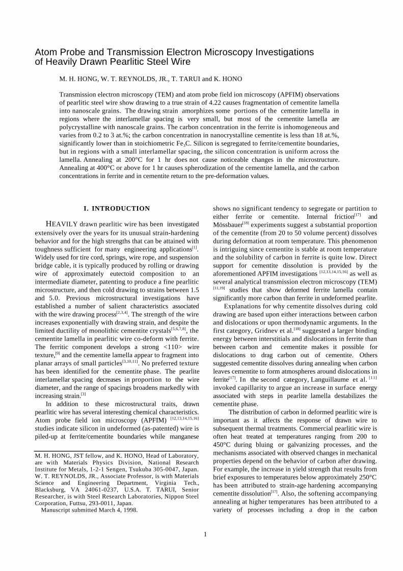
Fig. 1----Cross sectional (a) bright-field and (b) dark-fieldimages of patented pearlitic wire. The beam direction is close tothe [001] zone of ferrite. The image in (b) was obtained usingthe cementite reflection circled in (a).

3
mass spectra of Mn++ (27.5 amu) and Fe++ (27 and 28 amu)overlap. However, previous one-dimensional atom proberesults from the same material[16] showed the manganeseconcentration is uniform in both as-patented and deformedwire, so the comparatively small amount of manganese wasincluded together with the Fe component in the 3DAPanalysis. Silicon peaks in the mass spectrum occur betweenm/n=14-15 and there is no ambiguity in distinguishingthem from iron, assuming that all silicon atoms are ionizedas doubly charged ions. Detected carbon peaks were found atmass-to-charge ratios of 6 (C++) and 12 (C+ and C2
++), 18(C3
++), 24 (C2+ and C4
++) and 36 (C3+). In this study, the
carbon concentration was calculated by assuming them/n=12 peak results entirely from C+ (a negligiblecontribution from C2
++), and the ions at the m/n=24 peak areC2
+.
III. RESULTS
A. Transmission Electron Microscopy
Figure 1 shows bright field and dark field TEMmicrographs of the as-patented wire in cross sectional view
with the electron beam nearly parallel to the [001] ferritezone. The dark field image in Figure 1 (b) was obtainedusing the cementite reflection circled in the inset to Figure1 (a). The interlamellar spacing is uniform within a givencolony (approximately 130 nm) and the thickness of thecementite lamella is about 20 nm. Strain contrast iscommonly observed in the ferrite lamella, and planar defectscan also be found in the cementite lamella (indicated byarrows in Figure 1 (b)). The latter appear much like thestacking faults and slip traces seen in pearlitic cementitedeformed to low strains[5,6,7,8]. These observations indicatethere is some internal strain in the as-transformed pearlite.
Figure 2 shows cross sectional TEM micrographs of awire drawn to a true strain of 4.22. The pearlite lamellaexhibit a characteristic curled morphology first described byLangford[3], and it is evident the interlamellar spacing variessubstantially from one ferrite grain to another. In contrastto the single crystal lamella found in undeformed pearlite,the dark field image of the heavily deformed pearlite (Figure2(b)) shows the cementite lamella are fragmented intosmall grains. Individual dislocations are not resolvable atthis large strain, but strain contrast (at arrows in Figure3(a)) are found throughout the ferrite lamella. These are
(a)
200 nm
(b)
Fig. 2––––Cross sectional (a) bright-field and (b) dark-field images of wire drawn to a true strain of 4.22. The selected areadiffraction pattern (inset) includes sharp ferrite reflections as well as ring patterns. The cementite reflection used for the dark-fieldimage is circled.

4
believed to arise from regions in ferrite with relatively highdislocation densities. Selected area diffraction patterns, suchas the inset in Figure 2(b), include fairly sharp ferritereflections as well as rings corresponding to cementiteinterplanar spacings. Using microdiffraction with a nominalprobe size of 5 nm, it was concluded the rings result fromsmall, randomly oriented fragmented cementite grains. Thus,
the fragmented appearance of the cementite in the dark fieldimage of Figure 2(b) comes from imaging only a smallportion of the randomly oriented grains.
Occasionally, a diffuse halo was observed inmicrodiffraction patterns from regions where theinterlamellar spacing was particularly small (~ 10 nm) asshown in Figure 3 (b). There are several possibleexplanations for such a halo. A number of diffractingplanes in cementite have similar interplanar spacings, sorandomly oriented cementite grains could give rise to a halo.This explanation does not account well for the uniformityof the halo in Figure 3 (b) given the small volume sampledby the electron beam - a cylinder through the foil not muchlarger than 5 nm in diameter. Alternatively, the halo couldarise from an oxide layer on the foil. Although thispossibility cannot be ruled out, the fact that the halo wasonly observed at the thinnest of the cementite lamellasuggests it comes from an amorphous-like structure inregions of cementite that underwent the greatest deformation.
An HREM image taken from a region with a smallinterlamellar spacing is shown in Figure 4. The largeplastic strain in the wire made it difficult to obtain clearzone-axis patterns from either ferrite or cementite, butlattice fringes could still be obtained at various locations.The horizontal bands in the micrograph correspond to twocementite lamella. The fringes in these lamella and thediscrete spots in Fourier transforms of cementite regions(e.g., inset at bottom center of Figure 4) indicate most ofthe cementite is crystalline. Individual grains between 5 and10 nm can be seen within cementite lamella in agreementwith recent results reported by Languillaume[11]. Theabsence of clear spots in the Fourier transform obtainedfrom the left inset in Figure 4 suggests this particularportion of the cementite may be amorphous. Thediscontinuous nature of the two cementite lamella in Figure4 is worth noting. The upper lamella appears to terminatein the middle of the figure (it actually continues left of theregion shown in the micrograph) and the lower one has abreak where there is strong strain contrast in ferrite.Although termination of cementite lamella are common inundeformed pearlite, they are more common in drawn wireand are usually associated with strained regions in ferrite.No evidence was found for cracks in cementite, so thethinning and termination of the lamella evidently occurredthrough plastic deformation.
Figure 5 shows the effect of various annealingtreatments on the microstructure of the wire in longitudinalview. Annealing the wire at 200°C for 1 hr has little effecton the appearance of the microstructure. Figures 5 (a) and(b) are of as-drawn wire, and (c) and (d) are from wireannealed at 200°C for 1 hr. There are no appreciabledifferences between as-drawn wire and wire annealed at200°C for 1 hr. Strain contrast is still present in the ferritelamella after annealing at 200°C (Figure 5(c)), and thecementite still has a fragmented nanocrystalline structure(Figure 5(d)).
100 nm
(a)
(b)
Fig. 3––––(a) Contrast arising from regions of local strain(arrowed) found throughout the ferrite lamella. (b) A diffuse haloobtained with microdiffraction from a highly deformedcementite lamella. The true strain in the wire is 4.22.

5
Substantial microstructural changes take place duringannealing at 400°C for 1hr (Figures 5 (e) and (f)). Thelamellar microstructure is still present, but the interlamellarspacing appears coarser than in the as-drawn wire. Thecementite lamella are no longer continuous, and coarsenedcementite grains 20-30 nm in diameter are observed evenwithin the ferrite lamella. Some of the cementite grainshave coarsened to between 50 and 70 nm in diameter,arrowed in Figure 5(f). Figures 5 (g) and (h) show brightfield and dark field images of wire annealed at 500°C for 1 hr.The lamellar structure is completely destroyed byrecrystallization of ferrite and spherodization of cementite.Strong strain contrast in ferrite is no longer evident.
B. Atom Probe Field Ion Microscopy
Figures 6 (a) and (b) show 3DAP carbon maps in as-patented and in as-drawn wire, respectively. The dimensionsof the analyzed volumes are approximately 18 × 18 × 24nm in 6(a) and 18 × 18 × 21 nm in 6(b). Each dotrepresents a location at which a carbon specie was detected(ionized C, C2, C3, or C4); all other elements are omitted forclarity. The regions in Figure 6 with a relatively highdensity of carbon ions extending from the top to the bottomof the analyzed volumes correspond to cementite lamella.Ferrite is easily identified by its comparatively low densityof carbon atoms. The undeformed cementite lamella in
Figure 6 (a) is approximately 20 nm thick, and the deformedcementite lamella in Figure 6 (b) are 5 nm thick in goodagreement with thicknesses measured with TEM (Figures 1,2 and 5).
Local composition information can be obtained byanalyzing data extracted from a small “selected” volumewithin a 3DAP analysis region. The selected volume can bechosen to provide elemental maps, concentrations, orconcentration profiles along a direction within the 3DAPanalysis region. For clarity, the larger 3DAP analysisregions are omitted from subsequent figures and only theselected volumes are shown. Figure 7 (a) shows 3DAPelemental maps of carbon and silicon from the selectedvolume outlined by the small box in Figure 6 (a). Theorientation of the selected volume was chosen to reveal thecarbon and silicon concentration profiles perpendicular tothe pearlite lamella. The left side of Figure 7 (a) correspondsto a ferrite lamella in undeformed pearlite, and the right sidecorresponds to cementite. Under ideal conditions, the 3DAPis capable of positioning atoms in the analyzed volumewith an accuracy of about 0.2 nm. However, preferentialevaporation of cementite causes aberrations in the electricfield that degrade the spatial resolution of the instrument.Errors in positioning atoms in the present experiments areestimated to be less than 1 nm based on the abrupt changein carbon concentration at the ferrite/cementite boundaryfrom undeformed pearlite shown in Figure 7 (a).
5 nm
Fig. 4----A high-resolution TEM image taken from a region of deformed pearlite with a particularly small interlamellar spacing (thetrue strain is 4.22). The horizontal bands in the micrograph correspond to two cementite lamella.

6
Figure 7 (b) shows concentration depth profiles ofcarbon and silicon calculated from the same selected volumeused in Figure 7 (a). Two factors affect the accuracy of thecalculated concentrations: systematic errors associated withinstrumental parameters and sampling statistics. Anestimate of the systematic errors can be obtained from themeasured carbon concentration in undeformed cementite;this value is approximately 24 at.% (Figure 7 (b)), which isin good agreement with the expected stoichiometry ofcarbon in cementite (25 at.%). Thus, the carbon
concentrations determined from atom probe data are accurateto within a factor of approximately 0.05. Uncertaintiesarising from sampling statistics decrease with the number ofatoms used to calculate the concentrations. However,increasing the sample volume to improve the statisticalaccuracy sacrifices the spatial resolution of the measurement.Concentration profiles like the ones in Figure 7 (b) weredetermined using a moving average to strike a balance
~18 nm
~24
nm
~18 nm
(a)
~18 nm ~18 nm
~21
nm
(b)
Fig. 6----- 3DAP carbon maps of (a) undeformed and (b)deformed pearlitic wires. Each dot represents the location atwhich a carbon ion was detected.
(b)
(a)
100 nm
100 nm
(b)
(e)
100 nm
100 nm
(g)
(c) (d)
(f)
(h)
Fig. 5----The effect of annealing on the microstructure ofpearlitic wire drawn to a true strain of 4.22. Bright-field/dark-field pairs taken perpendicular to the wire axis (longitudinalview): as-drawn wire (a) and (b); annealed at 200°C for 1 hr (c)and (d); annealed at 400°C for 1 hr (e) and (f); annealed at500°C for 1 hr (g) and (h).

7
between statistical confidence and spatial detail. At eachdepth distance, the concentrations were calculated bycounting all the species in a block consisting of a layer 0.5nm thick times the width and height of the selected volume.A typical block contained about 500 atoms, and theconcentration profiles were obtained by moving the positionof the block from one end of the selected volume to theother. The concentrations vary by a factor of about 0.15from one depth to the next, and this “noise” is notstatistically significant. Larger concentration fluctuationsextending over a depth of a couple nanometers reflect
significant concentration variations involving severalthousand atoms.
In Figure 7 (b), the carbon concentration in ferrite isestimated to be 0.07 at.%, perhaps a little higher than theequilibrium carbon concentration at 560°C, i.e. 0.01 at.%.This result indicates the ferrite in patented pearlitic wiredoes not reach equilibrium and is slightly supersaturatedwith carbon[13,16] after patenting at 560°C for 30 sec. Theferrite/cementite boundary is relatively sharp and siliconappears to be enriched to a concentration of approximately 2at.% at the boundary.
Figure 8 shows a field ion micrograph of a wire drawnto a true strain of 4.22; the wire axis is perpendicular to theplane of the figure. The brightly imaging bands are ferritelamella, and the dark bands correspond to cementite lamella.In order to determine carbon concentrations in ferrite and incementite, two selected volumes located at A and B wereanalyzed by 3DAP.
Figure 9 (a) shows 3DAP elemental maps of carbon andsilicon in a selected volume 4 × 4 × 15 nm in size obtainedfrom region where the interlamellar spacing is very small(location A in Figure 8). The two cementite lamella areresolved along the analysis direction. The location ofcementite and ferrite can be recognized by the difference inthe density of carbon. Carbon-enriched regions correspond tocementite lamella and some carbon atoms appear to bepresent even in the ferrite region. The ferrite/cementiteinterface appears diffuse, but this may be due in part toevaporation aberration of ions originating from surfaces
0 3 6 9 12 150
Depth distance, nm
Si,
at%
5
C, a
t%
0
16
8
24
(b)
(a)
C
Si
~15 nm
~4 nm
~4 nm
~4 nm
~4 nm
~15 nm
Fig. 7----- (a) 3DAP elemental maps of carbon and silicon inthe selected volume outlined in Figure 6 (a). (b) Carbon andsilicon concentration profiles obtained from (a); eachnanometer of distance roughly corresponds to 1000 atoms.
~20 nm
Fig. 8----- A Ne field ion image of wire drawn to a true strainof 4.22. The brightly imaging bands are ferrite lamella, anddarkly imaging bands are cementite lamella. Regions at A andB were analyzed by 3DAP.

8
with slightly different local curvatures. The correspondingconcentration profiles are shown in Figure 9 (b). The carbonconcentration in cementite is approximately 16 at.%,considerably lower than the stoichiometry of cementite (25at.% C). On the other hand, the carbon concentration in theferrite ranges from 2 to 3 at.% and is significantly higherthan that observed in as-patented ferrite. This type ofanalysis was repeated several times, and a 2-3 at.% carbonconcentration in ferrite was reproducibly recorded. In theheavily deformed wire, silicon enrichment at theferrite/cementite interface is not observed in regions with a
small interlamellar spacing, Figure 9 (b). This resultindicates that silicon also undergoes some mixing duringthe wire drawing process.
Figure 10 (a) shows a set of carbon and silicon mapsobtained from location B in Figure 8. The interlamellarspacing in this region is somewhat coarser than that oflocation A. Consequently, only one cementite lamella isincluded within the selected volume. The carbonconcentration in ferrite in Figure 10 (b) is between 0.2 and1 at.%, and is considerably lower than that observed inferrite with a finer interlamellar spacing (c.f. 2 to 3 at.%).
(a)
0 3 6 9 12 150
Depth distance, nm
Si,
at%
5
C, a
t%
0
16
8
24
(b)
Si
~15 nm
C
~15 nm
~4 nm
~4 nm
~4 nm
~4 nm
Fig. 9----- (a) 3DAP elemental maps of carbon and siliconobtained from region A in Figure 8. (b) The correspondingcarbon and silicon concentration profiles across theferrite/cementite interface. Each nanometer of distance roughlycorresponds to 1000 atoms.
C, a
t%
0
16
8
24
0 3 6 9 12 150
Depth distance, nm
Si,
at%
5
(b)
C
Si
(a)~15 nm
~4 nm
~4 nm
~4 nm
~4 nm
~15 nm
Fig. 10---- (a) 3DAP elemental maps of carbon and siliconobtained from region B in Figure 12. (b) The correspondingcarbon and silicon concentration profiles across theferrite/cementite boundary. E); each nanometer of distanceroughly corresponds to 1000 atoms.

9
This result indicates the carbon concentration in heavilydrawn wire is very inhomogeneous, and it is higher wherethe interlamellar spacing is smaller. The silicon profile inFigure 10 suggests there is some silicon enrichment at theferrite/cementite interface.
A 3DAP elemental maps of carbon and siliconobtained from a wire drawn to ε=4.22 and aged at 200°C for1hr (Figure 11) are qualitatively the same as those of the as-drawn wire (Figure 9); there is still a substantial amount ofexcess carbon dissolved in the ferrite lamella and the carbonconcentration in cementite is still significantly lower than
stoichiometric Fe3C. There appears to be a tendency forsome silicon enrichment at the ferrite/cementite boundaries.
An FIM image of wire aged at 400°C for 1 hr isshown in Figure 12 (a). The brightly imaging regions areferrite, and cementite lies within the narrow, dark bands.The interlamellar spacing is greater than in as-drawn wire,in agreement with the TEM results shown in Figure 5. Theconcentric rings of the low index planes in ferrite are imagedmore clearly than in as-drawn wire (Figure 8), implying theferrite lattice has become less distorted, presumably fromless dissolved carbon. Such clear FIM images of ferrite aretypical for low alloy ferritic steels.
Figure 12 (b) shows 3DAP elemental maps of carbonand silicon in a wire aged at 400°C for 1 hr; theseconditions spherodize the cementite (refer to Figure 5). Theferrite/cementite boundary is clearly delineated by the carbondistribution. Figure 12 (c) shows the correspondingconcentration profiles of carbon and silicon calculated fromthe selected volume. The carbon concentration in thecementite is approximately 24 at.% and that in ferrite is0.07 at.%; these values are similar to those obtained fromthe as-patented (undeformed) wire. Enrichment of silicon isobserved at the ferrite/cementite interface, where the siliconconcentration is approximately 2 at.%. These resultssuggest spherodization of cementite at 400°C isaccompanied by recovery and/or recrystallization of ferriteand a loss of the excess carbon in ferrite.
IV. DISCUSSION
The most interesting result of the 3DAP analyses is thedirect evidence for cementite dissolution during cold-drawing.In wire drawn to a strain of 4.22, the average carbonconcentration in ferrite is approximately 2 at.%C, but thelocal concentration varies between 0.2 and 3 at.%. Inaddition, when ferrite regions exhibiting particularly clearFIM images are analyzed by atom probe, they invariablycontain low levels of carbon, and regions with distortedFIM images contain higher carbon concentrations. Thisdemonstrates that carbon is not dissolved in ferriteuniformly, but is probably bound to dislocations. TEMresults suggest the dislocation density in ferrite is notuniform after deformation of ε=4.22. Thus, the strongbinding of carbon to dislocations is a likely cause of theincrease in the apparent carbon concentration in ferrite, andwe conclude carbon segregates to dislocations or dislocationpile-ups in ferrite rather than dissolving in ferrite as auniform solid solution.
Previous Mössbauer [17] and HREM studies[11] suggestedcementite dissolution occurs during heavy deformation, andthe corresponding increase in carbon content in ferrite isexpected. The Mössbauer work reported 20 to 50% of thecementite can dissolve during cold work. 50% dissolution ofthe equilibrium fraction of cementite in pearlitic steel ofeutectoid composition requires an increase in the carbonconcentration in ferrite up to about 2.7 at%. Thus, the 2 to3 at.% carbon concentration in ferrite observed in this
C, a
t%
0
16
8
24
0 3 6 9 12 150
Depth distance, nm
Si,
at%
5
(b)
C
Si
(a)~15 nm
~4 nm
~4 nm
~4 nm
~4 nm
~15 nm
Fig. 11---- (a) 3DAP elemental maps of carbon and silicon in apearlitic wire (ε=4.22) aged at 200°C for 1hr. (b) Thecorresponding carbon and silicon concentration profilesacross the ferrite/cementite interface in (a). Each nanometer ofdistance roughly corresponds to 1000 atoms.

10
investigation is not surprising. However, a significantlylower than stoichiometric carbon concentration in deformedcementite is unexpected. The atom probe data indicates thecarbon concentration in cementite deformed to a strain of4.22 is approximately 16 at.%. Indirect evidence for a lowercarbon concentration in the cementite after deformation wasreported using EELS spectroscopy by Languillaume et al.[11],and recent 3DAP work by Danoix et al.[13] also reported thecarbon concentration of the cementite in the deformedpearlitic steel is lower than the stoichiometric value (~20at.%C). Because stoichiometric cementite was detected inthis investigation (in as-patented wire and in wire annealed
at or above 400°C), we believe the finding that deformedcementite contains significantly less than the stoichiometriccarbon concentration is unequivocal.
Equilibrated cementite has a narrow existence range withrespect to carbon concentration[22], so a decrease in theamount of carbon in cementite must be accompanied by theaddition of a high density of lattice defects in order to allowa deviation from stoichiometry. Electron microscopy studiesby Maurer[5], Gil Sevillano[6] and Inoue[7,8] establishedcementite lamella in pearlite deformed to somewhat lowerstrains contain numerous planar defects and slip bands. Inthis study, the drawing process reduces cementite lamella to
~20 nm(a)
(b)
C
Si
~15 nm
~4 nm
~4 nm
~4 nm
~4 nm
~15 nm
C, a
t%
0
16
8
24
0 3 6 9 12 150
Depth distance, nm
Si,
at%
5
(c)
Fig. 12 Pearlitic wire drawn to ε=4.22 and aged at 400°C for 1 hr. (a) Ne field-ion image, (b) 3DAP elemental mapsof carbon and silicon, and (c) the corresponding carbon and silicon concentration profiles across the ferrite/cementiteinterface in (b). Each nanometer of distance roughly corresponds to 1000 atoms.

11
a thickness of about 2 to 5 nm and introduces numerousboundaries between the cementite nanocrystals.
These boundaries, which are defective regions incementite, can be expected to arise when ferrite andcementite lamella are co-deformed to large strains becausethe dislocation Burgers vectors in the two phases differ.Reported slip systems in cementite (oP16 structure) at roomtemperature include (001)[010], (010)[001], and (100)[010][8], and slip traces have also been seen on the (011), and(110) planes as well[6]. The [010] and [001] cementiteBurgers vectors are 0.509 nm and 0.647 nm, respectively,considerably different from the 0.2485 nm Burgers vector inferrite. There are, however, twelve inter-iron distances incementite within 5% of a ferrite Burger’s vector. Slip alongany of these directions amounts to a partial dislocation incementite. At least some of these additional slip directionsmust be active or there would not be enough slip systemsfor ferrite and cementite to deform compatibly.Consequently, the transfer of plastic strain from ferrite tocementite should be accompanied by the creation of stackingfaults and vacancies, and at sufficient densities, these defectsshould allow the carbon concentration in cementite todeviate from stoichiometry. The appearance of occasionalamorphous regions along cementite lamella also may berelated to the incommensurate Burgers vectors in ferrite andcementite if extensive slip across a ferrite/cementiteboundary can produce enough structural disorder to causeamorphization. High strains accompanying mechanicalalloying have been shown to produce solid stateamorphization of Fe75C25 powders[23, 24], so it seemsreasonable to expect a 4.22 drawing strain to amorphizesome cementite in drawn pearlitic wire.
Although low temperature annealing at 200°C wasreported to increase yield strength[16], no noticeablemicrostructural changes were detected in either ferrite orcementite with TEM and APFIM. The atom probe data donot provide clear evidence of continuing cementitedissolution during annealing at 200°C as Yamadasuggested[16]. As the carbon concentration is not uniform inferrite, quantifying the average carbon concentration inferrite is not easy. The measured concentration varies greatlyfrom one place to another, and it is thus difficult toconclude whether the carbon concentration in ferrite hasincreased during annealing at 200°C. It seems more likelythat the increase in yield strength accompanying annealingat 200°C results from the locking of mobile dislocations bycarbon atoms in ferrite.
Annealing at 400 and 500°C causes substantial changesin the microstructure and distribution of carbon, and thesechanges readily explain the drop in the strength of drawnwire[14]. The scale of the microstructure coarsens ascementite spherodizes, the spacing of the prior cementitelamella increases, and the ferrite recovers and recrystallizes.All of these microstructural changes lead to a decrease in theresistance to plastic flow. The return of the carbonconcentration in ferrite to the pre-deformation level removes
any solid-solution strengthening that might have resultedfrom carbon in the as-drawn ferrite.
Previous studies of the role of silicon duringannealing of drawn pearlitic wire showed Si increases theresistance to softening at high annealing temperatures bysuppressing spherodization of cementite lamella[14, 15, 18]].From the present investigation, it appears that thisbeneficial effect of Si is related to its tendency to segregateto the ferrite/cementite boundaries during annealing, even attemperatures as low as 200°C. Once a layer of excesssilicon develops at ferrite/cementite boundaries, the break-upof cementite during spherodization can be expected to becontrolled by the relatively sluggish diffusion of silicon.
V. CONCLUSIONS
1. The cementite lamella in pearlitic wire drawn to a strainof 4.22 is polycrystalline with grains as small as 2-5nm. Some amorphized cementite is found in regionswith the smallest interlamellar spacing, but most of thecementite is crystalline.
2. The carbon concentration in ferrite in drawn wire(ε=4.22) is significantly higher than the equilibriumsolubility of carbon in ferrite. The carbon distributionin ferrite is not uniform and ranges from 0.2 to 3 at.%.Heterogeneous dissolution of carbon in ferrite suggeststhat carbon is segregated to dislocations or dislocationpile-ups.
3. Heavy deformation during wire drawing decreases thecarbon concentration in cementite significantly (to ~16at.%).
4. Si is segregated at ferrite/cementite interfaces in as-patented wire. Heavy deformation during cold drawingapparently produces enough mechanical mixing toremove much of the segregation.
5. Annealing at 200°C does not cause any detectablechange in the TEM microstructure nor the chemicaldistribution observed by APFIM despite the fact thisheat treatment is reported to increase the yield strength.Thus, the increase in strength accompanying annealingat 200°C is concluded to result from the locking ofmobile dislocations by carbon atoms in ferrite.
6. Annealing at 400°C and 500°C changes themicrostructure drastically: cementite spherodizes, ferriterecovers and recrystallizes. The carbon concentrations incementite and ferrite return to the same values as inundeformed pearlite.
ACKNOWLEDGMENTS
This work was partially supported by the FrontierResearch Center for Structural Materials at the NationalResearch Institute for Metals and the International JointResearch Grant by NEDO. M. H. Hong gratefullyacknowledge the Japan Science and Technology Agency forthe JST fellowship, and W. T. Reynolds acknowledgesUnited States National Science Foundation (DMR 9303518

12
and INT 9600383) for financial support. The authors thankK. Tsuzaki and T. Takahashi for valuable discussions, andM. Murayama for assistance with the APFIM experimentsand data analysis.
REFERENCES
1. H. G. Paris: Metallurgy, Processing andApplications of Metal Wires, H. G. Paris and D. K.Kim ed., TMS, Warrendale, PA, 1996, pp. 3-15.
2. J. D. Embury and R. M. Fisher: Acta Metall.,1966, vol. 14, pp. 147-59.
3. G. Langford, Metall. Trans. 1977, vol. 8A, pp.861-75.
4. W. J. Nam and C. M. Bae; Mater. Sci. and Eng. A,1995, vol. 203, pp. 278-85.
5. K. Maurer and D. H. Warrington, Phil. Mag.,1967, vol. 15, pp. 321-27
6. J. Gil Sevillano: Material Sci. and Eng., 1975, vol.20, pp. 221-25.
7. A. Inoue, T. Ogura, and T. Masumoto: ScriptaMetal., 1976, vol. 11, pp. 1-5.
8. A. Inoue, T. Ogura, and T. Masumoto: Trans. JIM,1977, vol. 17, pp. 149-57.
9. K. Van Acker, J. Root, P. Van Houtte and E.Aernoudt: Acta Mater., 1996, vol. 44, pp. 4039-49.
10. D. A. Porter, K. E. Easterling, and G. D. W.Smith: Acta Metall., 1978, vol. 26, pp. 1405-22.
11. J. Languillaume, G. Kapelski, and B. Baudelet:Acta Mater., 1997, vol. 45, pp. 1201-12.
12. A. R. Waugh, S. Paetke, and D. V. Edmonds:Metallography, 1981, vol. 14, pp. 237-51.
13. F. Danoix, X. Sauvage, D. Julien, and J.Copreaux: Mater. Sci. Eng. A, 1998, in press.
14. T. Tarui, T. Takahashi, S. Ohashi, and R. Uemori:Iron and Steelmaker, 1994, vol. 21, pp. 25-30.
15. T. Tarui, T. Takahashi, H. Tashiro, and S.Nishida: Processing and Applications of MetalWires, H. G. Paris and D. K. Kim ed., TMS,Warrendale, PA, 1996, pp. 87-96.
16. H. G. Read, W. T. Reynolds Jr., K. Hono, and T.Tarui: Scripta Meter., 1997, vol. 37, pp. 1221-30.
17. Y. Yamada: Trans. ISIJ, 1976, vol. 16, pp. 417-26.18. V. N. Gridnev, V. V. Nemoshkalenko, Yu. Ya.
Meshkov, V. G. Gavrilyuk, V. G. Prokopenko,and O. N. Razumov: Phys. Stat. Sol. A, 1975,vol. 31, pp. 201-210.
19. K. Makii, H. Yaguchi, M. Kaiso, N. Ibaraki, Y.Miyamoto , and Y. Oki: Scripta Mater., 1997, vol.37, pp. 1753-59.
20. H. Suto and T. Kudo: J. Jap. Inst. Met., 1972,vol. 36, pp. 693-701.
21. D. Blavette, B. Deconihout, A. Bostel, J. M.Sarrau, M. Bouet, and A. Menand: Rev. Sci.Instrum., 1993, vol. 64, 2911-19.
22. F. X. Kayser and Y. Sumitomo: J. PhaseEquilibria, 1997, vol. 18, no. 5, pp. 458.
23. T. Nasu, C. C. Koch, K. Nagaoka, N. Itoh, M.Sakurai, and K. Suzuki: Mater. Sci. Eng. A, 1991,vol A134, pp. 1385-88.
24. T. Tanaka, T. Nasu, K. N. Ishihara, and P. H.Shingu: J. Less-Comm Metals, 1991, vol 171, pp.237-47.