Embed Size (px)
Citation preview

Atmel ATFEE560
Multi-Chip Rad-Hard Modules:
Reprogrammable FPGA matrix (ATF280) (x2)
EEPROM Memory (AT69170) (x2)
DATASHEET
Features
Non Volatile Rad Hard Reprogrammable FPGA
ATF280 SRAM-based FPGA
AT69170 Serial EEPROM
2x SRAM-based FPGA designed for Space use - ATF280
560K equivalent ASIC gates
28,800 cells ( two 3-input LUT or one 4-input LUT, one DFF)
Unlimited reprogrammability
SEE-hardened (Configuration RAM, DPRAM, DFF, I/O buffers)
Rad Hard by Design - No need for mitigation techniques during design
Available DPRAM ressources in the ATF280
230,400 bits of distributed RAM
Organized in 32x4 blocks of DPRAM
Independent of Logic Cells
Single/Dual port capability
Reset System
Individual reset on each FPGA
Possibility to reset simultaneously both FPGAs
Clock System
2 global clocks shared between both FPGAs
6 global clocks and 2 fast clocks on FPGA 1
6 global clocks and 2 fast clocks on FPGA 2
Flexible serial configuration
Integrated 4Mbits serial non volatile memory
On chip redundant configuration memory
Designed to store Field Programmable Gate Arrays Configurations
In-System Programming (ISP) via Two-Wire Interface
Master/Slave configuration capability
Configuration Integrity Check
Check of the data during FPGA application download
Self Integrity Check (CSIC) of the configuration during FPGA operation
User IOs
Cold-sparing and PCI-compliant I/Os:
24 General Purpose IOs internally shared by both FPAGs and externally
accessible
131 General Purpose IOs internally shared by both FPAGs
107 General Purpose IOs only for FPGA1
41041BAERO09/15

ATFEE560 [DATASHEET] 41041BAERO09/15
2
146 General Purpose IOs only for FPGA2
4 LVDS transmitters on FPGA2
4 LVDS receivers on FPGA2
Performance
50MHz system performance
10ns 32X4 DPRAM access time
Operating range
Voltages
1.65V to 1.95V (Core)
3V to 3.6V (Clustered I/Os)
Temperature
- 55°C to +125°C
Radiation performance
Total dose tested up to 60 krads (Si)
AT69170, TID tested up to 60 krads (unbiased)
ATF280, TID tested up to 300 krads
No single event latch-up below a LET of 95 MeV/mg/cm2
ESD better than 2000V for I/O and better than 1000V for LVDS
Quality grades
QML-Q or V
Description
The ATFEE560 is a radiation-hardened reprogrammable FPGA, especially designed for
space applications. For low-power consumption applications, the ATFEE560 is a new
device offering many advantages.
The ATFEE560 relies on Atmel ATF280 space qualified SRAM based FPGA together with
the Atmel AT69170 serial configuration EEPROM memory.
The ATFEE560 features an innovative built-in SEU protection, which eliminates the need
for Triple-Module-Redundancy (TMR). Its re-programmability makes multiple design
iterations possible. Moreover, post-programming burn-in is not necessary.
With the integration of redundant serial programming eeproms inside the package, the
ATFEE560 is perfectly suited for application requiring small footprint.
The Development Kit lets to evaluate the ATFEE560 quickly and economically, running
simple demonstrations as well as your complete applications. Throughout your
development, from concept to final integration, Atmel provides the tools and support to
help you successfully integrate your application into the ATFEE560.
The ATFEE560 is available in MQFP352 package and features 277 standard I/Os and 8
LVDS I/Os (4 Rx and 4Tx) for the user application.
Table 1. ATFEE560 Summary
Function ATFEE560
Available ASIC Gates (50% typ. routable) 2x 280K / 560K
RAM Bits 2x 115 200 / 230 400
Core Cells 2x 14 400 / 28 800
I/O 277
LVDS (Rx/Tx) 4 Rx / 4 Tx

ATFEE560 [DATASHEET] 41041BAERO09/15
3
Figure 2. ATFEE560 Overview
DATACLK/CE/RESET_OE
READYSER_EN
Internally shared
IO[130:0]
IO_FPGA2
[144:0]FPGA2
ILVDS[3:0]
ILVDSn[3:0]
OLVDS[3:0]
OLVDSn[3:0]
IO_FPGA1
[105:0]
Serial Cfg Interface
INIT
CO
NC
CL
KD
0
INIT
CO
NC
CL
KD
0
Serial Cfg Interface
CSOUT
CS0
Cascading
Interface
M2
M1
M0
Mode
RESETN
FPGA_1
FPGA_2
NVM_1
NVM_2
M2
M1
M0
Mode
RESETN
Mode
FPGA1
Mode
FPGA2
Reset
FPGA1
Reset
FPGA2
Cascading
Interface
INIT
_F
1C
ON
CC
LK
D0
RE
AD
YS
ER
_E
N
Internally shared
IO[130:0]
Internally shared
IO[23:0]
External access of
shared IO[23:0]
Internally shared
IO[23:0]
INIT
_F
2
References
ATF280 Datasheet – ref : doc7750
AT69170 Datasheet – ref : doc41069

ATFEE560 [DATASHEET] 41041BAERO09/15
4
Table of Contents
1. Glossary ............................................................................................. 5
2. Dies connections ................................................................................ 6
2.1 PINOUT ............................................................................................................ 6 2.1.1 FPGA1 ............................................................................................. 6
2.1.1.1 General Purpose IOs ........................................................ 6 2.1.1.2 Supply ............................................................................... 7 2.1.1.3 Configuration IOs .............................................................. 7
2.1.2 FPGA2 ............................................................................................. 8 2.1.2.1 General Purpose IOs ........................................................ 8 2.1.2.2 LVDS ............................................................................... 9 2.1.2.3 Supply ............................................................................. 10 2.1.2.4 Configuration IOs ............................................................ 10
2.1.3 Pins shared by both FPGAs .............................................................. 10 2.1.3.1 General Purpose Ios ....................................................... 10 2.1.3.2 Configuration IOs ............................................................ 11
2.1.4 NVM_1 and NVM_2 .......................................................................... 12 2.1.4.1 Configuration IOs ............................................................ 12 2.1.4.2 Supply ............................................................................. 12
2.1.5 Pins shared by both memories and both FPGA ................................ 12 2.1.6 JTAG ........................................................................................... 13
2.2 IOs from both FPGAs connected internally ..................................................... 13
3. Configuration Download ................................................................... 15
3.1 Master serial mode – Mode 0 .......................................................................... 15 3.2 Slave serial mode – mode 1 ............................................................................ 16 3.3 Available ATFEE560 configurations ................................................................ 16
3.3.1 FPGA1 master – FPGA2 slave ......................................................... 16 3.3.2 FPGA1 slave – FPGA2 slave ............................................................ 19
4. Ordering Information ........................................................................ 20
4.1 ATFEE560FF Ordering Codes ........................................................................ 20 4.2 ATFEE560 Evaluation Kit Ordering Codes ..................................................... 20
5. Revision History ............................................................................... 21

ATFEE560 [DATASHEET] 41041BAERO09/15
5
1. Glossary
FPGA Field Programmable Gate Array
POR Power On Reset
SRAM Static Random Access Memory
SEU Single Event Upset
CSIC Configuration Self Internal Checker
TWI Two wire Interface
ATFEE560 [DATASHEET] 41041BAERO09/15
6
2. Dies connections
The aim here is to describe all the IO connections for each die implemented in the ATFEE560 ( 2x ATF280 and 2x
AT69170). The serial programmation mode has been privileged due to the limited number of pakages pins.
Both FPGA have three connection types for their General Purpose IOs, here after their descriptions and their number:
24 General Purpose IOs internally shared by both FPAGs and externally accessible
131 General Purpose IOs internally shared by both FPAGs
107 General Purpose IOs dedicated to FPGA1 and 146 General Purpose IOs dedicated to FPGA2 (including
INIT signals)
Each FPGA and each non-volatile memory has a dedicated supply.
2.1 PINOUT
2.1.1 FPGA1
2.1.1.1 General Purpose IOs
Table 2-1. FPGA1, General Purpose IOs
IO MQFP352 IO MQFP352 IO MQFP352 IO MQFP352
IO1_GCK1 10 IO79 39 IO173 70 IO259_LDC (*) 103
IO5 11 IO83 40 IO175 71 IO263 104
IO7 12 IO85 41 IO177 72 IO265_HDC (*) 105
IO11 13 IO87 42 IO180_FCK2 73 IO267 106
IO13 14 IO93 43 IO185 74 IO273 108
IO17 15 IO97 44 IO187 75 IO277 109
IO19 16 IO99 47 IO191 76 IO279 110
IO23 17 IO103 48 IO193 77 IO283 113
IO25 18 IO105 49 IO197 78 IO480_GCK4 114
IO27 19 IO111 50 IO199 79 IO722_GCK7 116
IO31 20 IO125 51 IO203 80 IO917 135
IO33 21 IO127 52 IO205 81 IO919 136
IO37 22 IO131 53 IO207 82 IO923 137
IO39 25 IO133 54 IO213 83 IO925 138
IO43 26 IO137 55 IO217 84 IO927 139
IO45 27 IO139 56 IO219 85 IO931 140
IO47 28 IO143 57 IO223 86 IO937 141
IO51 29 IO145 58 IO227 92 IO939 142
IO53 30 IO147 59 IO231 93 IO943 143
IO57 31 IO151 60 IO233 94 IO945 144
IO61_FCK1 32 IO153 61 IO237 95 IO947 145
IO63 33 IO157 62 IO240_GCK2 96 IO951 146
IO65 34 IO159 63 IO245 98 IO953 147
ATFEE560 [DATASHEET] 41041BAERO09/15
7
IO67 35 IO163 64 IO247 99 IO960 149
IO71 36 IO165 65 IO251 100 IO303_INIT (*) 150
IO73 37 IO167 66 IO253 101 IO547_CS0 (*) 267
IO77 38 IO171 69 IO257 102
(*) : this general purpose IO is a configuration IO during configuration download
2.1.1.2 Supply
Table 2-2. FPGA1, supply
GROUND MQFP352 VDD = 1,8V MQFP352 VCC = 3,3V MQFP352
GND 1 VDD 2 VCC 24
GND 23 VDD 46 VCC 68
GND 45 VDD 88 VCC 112
GND 67 VDD 90
GND 87 VDD 134
GND 89 VDD 352
GND 111
GND 133
GND 156
2.1.1.3 Configuration IOs
Table 2-3. FPGA1, configuration IOs
Configuration IO name MQFP352
M0 7
M1 8
M2 9
IO259_LDC 103
IO265_HDC 105
IO303_INIT 150
IO547_CS0 267
RESETN 342

ATFEE560 [DATASHEET] 41041BAERO09/15
8
2.1.2 FPGA2
2.1.2.1 General Purpose IOs
Table 2-4. FPGA2, General purpose IOs
IO MQFP352 IO MQFP352 IO MQFP352 IO MQFP352
IO1_GCK1 153 IO507 205 IO625 256 IO757 300
IO399 163 IO511 206 IO639 257 IO759 301
IO403 164 IO513 207 IO643 258 IO763 302
IO405 165 IO517 208 IO645 259 IO765 303
IO407 166 IO519 209 IO647 260 IO767 304
IO411 167 IO523 210 IO651 261 IO771 305
IO413 168 IO525 211 IO653 262 IO773 306
IO417 169 IO527 212 IO658_FCK4 268 IO777 307
IO419 170 IO531 213 IO661 269 IO779 308
IO423 171 IO533 214 IO665 270 IO783 311
IO425 172 IO537 215 IO667 271 IO785 312
IO427 173 IO539 216 IO671 272 IO787 313
IO303_INIT (*) 174 IO543_FCK3 217 IO673 273 IO791 314
IO433 179 IO545 218 IO677 274 IO793 315
IO437 180 IO551 220 IO679 275 IO797 316
IO439 181 IO553 223 IO683 276 IO799 317
IO443 182 IO557 224 IO685 277 IO803 318
IO445 183 IO559 225 IO687 278 IO805 319
IO447 184 IO563 226 IO691 279 IO807 320
IO453 185 IO565 227 IO693 280 IO811 321
IO457 186 IO567 228 IO697 281 IO813 322
IO459 187 IO571 229 IO699 282 IO817 323
IO463 188 IO573 230 IO703 283 IO819 324
IO465 189 IO577 231 IO705 284 IO823 325
IO467 190 IO579 232 IO707 285 IO825 326
IO471 191 IO583 233 IO711 286 IO831 327
IO473 192 IO585 234 IO717 289 IO833 328
IO477 193 IO591 235 IO720_GCK6_CSOUTN
(*) 290 IO847 329
IO480_GCK4 194 IO605 244 IO722_GCK7 291 IO851 330
IO482_GCK5 195 IO607 245 IO725 292 IO853 333
IO485 196 IO611 246 IO733 293 IO857 334
IO487 197 IO613 249 IO737 294 IO859 335

ATFEE560 [DATASHEET] 41041BAERO09/15
9
IO491 198 IO617 250 IO739 295 IO863 336
IO493 201 IO619 251 IO745 296 IO865 337
IO497 202 IO623 252 IO747 297 IO960_GCK8_ 338
IO503 203 IO627 254 IO751 298
IO505 204 IO633 255 IO753 299
(*) : this general purpose IO is also a configuration IO during configuration download
2.1.2.2 LVDS
Table 2-5. FPGA2, LVDS IO
LVDS IOs MQFP352
LVDS_Vref 6
ILVDS3 154
ILVDS3N 155
ILVDS4 157
ILVDS4N 158
OLVDS3 159
OLVDS3N 160
OLVDS4 161
OLVDS4N 162
ILVDS5 236
ILVDS5N 237
ILVDS6 238
ILVDS6N 239
OLVDS5 240
OLVDS5N 241
OLVDS6 242
OLVDS6N 243
LVDS_Vref 345
ATFEE560 [DATASHEET] 41041BAERO09/15
10
2.1.2.3 Supply
Table 2-6. FPGA2 supply
GROUND MQFP352 VDD = 1,8V MQFP352 VCC = 3,3V MQFP352
GND 199 VDD 176 VCC 200
GND 221 VDD 178 VCC 248
GND 247 VDD 222 VCC 288
GND 263 VDD 264
GND 265 VDD 266
GND 287 VDD 310
GND 309
GND 331
GND 351
2.1.2.4 Configuration IOs
Table 2-7. FPGA2, configuration IOs
Configuration IO name MQFP352
IO303_INIT 174
IO720_GCK6_CSOUTN 290
M0 347
M1 348
M2 349
RESETN 343
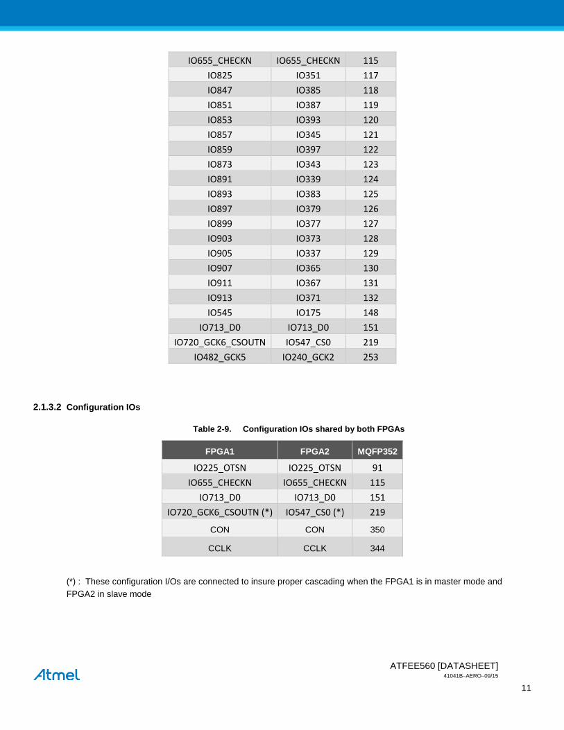
2.1.3 Pins shared by both FPGAs
2.1.3.1 General Purpose Ios
24 General purpose IOs are shared by both FPGAs and externally accessible.
Table 2-8. General purpose IO shared by both FPGAs
FPGA1 FPGA2 MQFP352
IO225_OTSN IO225_OTSN 91
IO241_GCK3 IO241_GCK3 97
IO271 IO637 107
ATFEE560 [DATASHEET] 41041BAERO09/15
11
IO655_CHECKN IO655_CHECKN 115
IO825 IO351 117
IO847 IO385 118
IO851 IO387 119
IO853 IO393 120
IO857 IO345 121
IO859 IO397 122
IO873 IO343 123
IO891 IO339 124
IO893 IO383 125
IO897 IO379 126
IO899 IO377 127
IO903 IO373 128
IO905 IO337 129
IO907 IO365 130
IO911 IO367 131
IO913 IO371 132
IO545 IO175 148
IO713_D0 IO713_D0 151
IO720_GCK6_CSOUTN IO547_CS0 219
IO482_GCK5 IO240_GCK2 253
2.1.3.2 Configuration IOs
Table 2-9. Configuration IOs shared by both FPGAs
FPGA1 FPGA2 MQFP352
IO225_OTSN IO225_OTSN 91
IO655_CHECKN IO655_CHECKN 115
IO713_D0 IO713_D0 151
IO720_GCK6_CSOUTN (*) IO547_CS0 (*) 219
CON CON 350
CCLK CCLK 344
(*) : These configuration I/Os are connected to insure proper cascading when the FPGA1 is in master mode and
FPGA2 in slave mode

ATFEE560 [DATASHEET] 41041BAERO09/15
12
2.1.4 NVM_1 and NVM_2
2.1.4.1 Configuration IOs
Table 2-10. Memories, configuration IOs
NVM_1 NVM_2 MQFP352
OE OE 150
DATA DATA 151
CLK CLK 344
CE CE 350
EN EN 339
READY READY 340
2.1.4.2 Supply
Table 2-11. Memories supply
NVM_1 NVM_2 MQFP352
GND 175
VDD = 3,3V 332
GND 177
VDD = 3,3V 152
The power pins are used to select NVM_1 or NVM_2 as configuration memory. The supplied memory download the
configuration data for both FPGAs. The other memory is in spare.
2.1.5 Pins shared by both memories and both FPGA
Table 2-12. Configuration IOs shared by both memories and both FPGAs
FPGA1 FPGA2 NVM_1 NVM_2 MQFP352
INIT OE OE 150
D0 D0 DATA DATA 151
CCLK CCLK CLK CLK 344
CON CON CE CE 350

ATFEE560 [DATASHEET] 41041BAERO09/15
13
2.1.6 JTAG
The JTAG feature of the ATFEE560 is done by chaining the JTAG of both FPGAs internally.
TRST, TMS and TCK input pins are shared between both FPGAs.
Caution: Due to ATF280 JTAG non functionality, use of the JTAG IOs is not possible. To avoid any misfunction
of the ATFEE560, it is required to apply the following polarities on each JTAG IOs.
Table 2-13. JTAG IOs
FPGA1 FPGA2 MQFP352 Polarity
TCK TCK 341 VCC or pull-up
TRST TRST 346 VCC or pull-up
TMS TMS 5 VCC or pull-up
TDI 3 VCC or pull-up
TDO 4 Left unconnected
2.2 IOs from both FPGAs connected internally
131 General purpose IOs are shared by both FGPAs but only connected internally
Table 2-14. IOs connected internally
FPGA1 FPGA2 IDS_label FPGA1 FPGA2 IDS_label FPGA1 FPGA2 IDS_label
IO393 IO327 N14 IO533 IO187 G6 IO687 IO33 G14
IO397 IO325 N13 IO537 IO185 K5 IO691 IO31 E10
IO399 IO323 K14 IO539 IO180 K6 IO693 IO27 G12
IO403 IO319 M13 IO543 IO177 K4 IO697 IO25 B10
IO405 IO317 L14 IO551 IO171 E8 IO699 IO23 B13
IO407 IO313 L13 IO553 IO167 F10 IO703 IO19 A11
IO411 IO311 H14 IO557 IO165 F8 IO705 IO17 C13
IO413 IO307 L12 IO559 IO163 C8 IO707 IO13 F14
IO417 IO305 J13 IO563 IO159 G8 IO711 IO11 D13
IO419 IO299 P11 IO565 IO157 F9 IO717 IO7 E13
IO423 IO297 K13 IO567 IO153 D7 IO725 IO5 H6
IO425 IO293 L11 IO571 IO151 J11 IO727 IO957 G5
IO427 IO291 P13 IO573 IO147 E7 IO731 IO953 G7
IO431 IO287 K11 IO577 IO145 H11 IO733 IO951 F5
IO433 IO285 M10 IO579 IO143 F7 IO737 IO947 E4
IO437 IO283 H12 IO583 IO139 F6 IO739 IO945 B5
IO439 IO279 N10 IO585 IO137 H8 IO743 IO943 D5
IO443 IO277 G11 IO591 IO133 E6 IO745 IO939 A8

ATFEE560 [DATASHEET] 41041BAERO09/15
14
IO445 IO273 N9 IO605 IO131 G10 IO747 IO937 A9
IO447 IO271 M9 IO607 IO127 D6 IO751 IO931 D4
IO453 IO267 N12 IO611 IO125 H10 IO753 IO927 B8
IO457 IO265 L10 IO613 IO111 J10 IO757 IO925 C4
IO459 IO263 N11 IO617 IO105 G9 IO759 IO923 C10
IO463 IO259 P10 IO619 IO103 C7 IO763 IO919 D3
IO465 IO257 M11 IO623 IO99 H9 IO765 IO917 B9
IO467 IO253 K12 IO625 IO97 E11 IO767 IO913 B4
IO471 IO251 K10 IO627 IO93 J8 IO771 IO911 A7
IO473 IO247 F11 IO633 IO87 C6 IO773 IO907 D2
IO477 IO245 J9 IO637 IO85 D10 IO777 IO905 B7
IO485 IO237 J7 IO639 IO83 G13 IO779 IO903 C2
IO487 IO233 P3 IO643 IO79 C11 IO783 IO899 B6
IO491 IO231 J4 IO645 IO77 H13 IO785 IO897 B3
IO493 IO227 J5 IO647 IO73 D12 IO787 IO893 C5
IO497 IO431 J3 IO651 IO71 A12 IO791 IO891 B2
IO503 IO223 G4 IO653 IO67 B12 IO793 IO887 A5
IO505 IO219 H4 IO658 IO63 E5 IO797 IO885 C1
IO507 IO217 H5 IO661 IO61 E12 IO799 IO883 A4
IO511 IO213 J6 IO665 IO57 H7 IO803 IO879 A3
IO513 IO207 G3 IO667 IO53 D11 IO805 IO873 D1
IO517 IO205 D9 IO671 IO51 J12 IO807 IO871 A2
IO519 IO203 F4 IO673 IO47 A13 IO811 IO867 E3
IO523 IO199 E9 IO677 IO45 F13
IO525 IO197 L1 IO679 IO43 A10
IO527 IO193 C9 IO683 IO39 F12
IO531 IO191 L2 IO685 IO37 B11
ATFEE560 [DATASHEET] 41041BAERO09/15
15
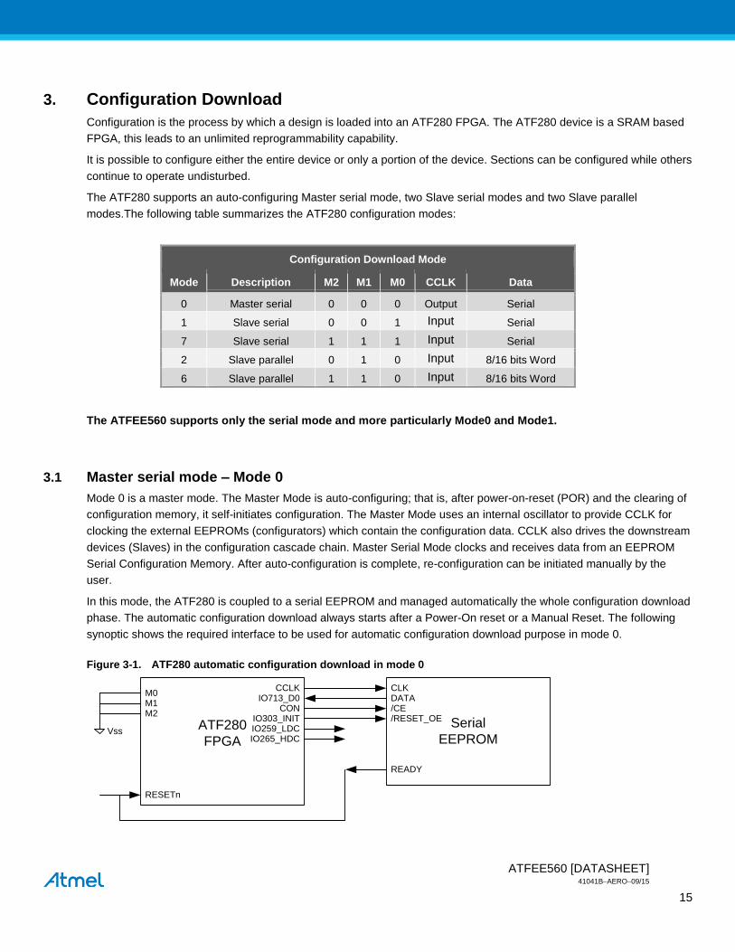
3. Configuration Download
Configuration is the process by which a design is loaded into an ATF280 FPGA. The ATF280 device is a SRAM based
FPGA, this leads to an unlimited reprogrammability capability.
It is possible to configure either the entire device or only a portion of the device. Sections can be configured while others
continue to operate undisturbed.
The ATF280 supports an auto-configuring Master serial mode, two Slave serial modes and two Slave parallel
modes.The following table summarizes the ATF280 configuration modes:
Configuration Download Mode
Mode Description M2 M1 M0 CCLK Data
0 Master serial 0 0 0 Output Serial
1 Slave serial 0 0 1 Input Serial
7 Slave serial 1 1 1 Input Serial
2 Slave parallel 0 1 0 Input 8/16 bits Word
6 Slave parallel 1 1 0 Input 8/16 bits Word
The ATFEE560 supports only the serial mode and more particularly Mode0 and Mode1.
3.1 Master serial mode – Mode 0
Mode 0 is a master mode. The Master Mode is auto-configuring; that is, after power-on-reset (POR) and the clearing of
configuration memory, it self-initiates configuration. The Master Mode uses an internal oscillator to provide CCLK for
clocking the external EEPROMs (configurators) which contain the configuration data. CCLK also drives the downstream
devices (Slaves) in the configuration cascade chain. Master Serial Mode clocks and receives data from an EEPROM
Serial Configuration Memory. After auto-configuration is complete, re-configuration can be initiated manually by the
user.
In this mode, the ATF280 is coupled to a serial EEPROM and managed automatically the whole configuration download
phase. The automatic configuration download always starts after a Power-On reset or a Manual Reset. The following
synoptic shows the required interface to be used for automatic configuration download purpose in mode 0.
Figure 3-1. ATF280 automatic configuration download in mode 0
ATF280
FPGA
M0M1M2
Vss
RESETn
CCLKIO713_D0
CONIO303_INITIO259_LDCIO265_HDC
Serial
EEPROM
CLKDATA/CE/RESET_OE
READY

ATFEE560 [DATASHEET] 41041BAERO09/15
16
3.2 Slave serial mode – mode 1
In slave mode, configuration is always initiated by another device. Data is applied to the device on the rising edge of
CCLK. In Slave Serial Mode, the device receives serial configuration data.
In mode 1, the ATF280 is coupled to a serial EEPROM and shall be externally driven for configuration download
purpose. The following synoptic shows the required interface to be used for configuration download purpose in mode 1.
Figure 3-2. ATF280 FPGA environment : configuration download in mode 1
ATF280
FPGA
M0M1M2
RESETn
Serial
EEPROM
CLKDATA/CE/RESET_OE
READY
External Component to
start Configuration
Download
Reset EEPROM
counters
Start configuration
downloadUser applies a low logic level
before starting configuration
download
IO547_CS0
Vss
VccCCLK
IO713_D0CON
IO303_INITIO259_LDCIO265_HDC
3.3 Available ATFEE560 configurations
The following choices has been done to implement both FPGAs in the product :
The FPGA 1 can be master (mode 0) or slave (mode 1).
The FPGA 2 can be only slave (mode 1).
FPGA1 in master mode : FPGA1 and FPGA2 are cascaded
3.3.1 FPGA1 master – FPGA2 slave
Table 3-1. Configuration Mode selection
FPGA1 FPGA2
M0 0 1
M1 0 0
M2 0 0
CCLK output input

ATFEE560 [DATASHEET] 41041BAERO09/15
17
Figure 3-3. ATFEE560 connections overview
Both FPGA are cascaded (CR2 of configuration register activate for both FPGA). FPGA1 initiates the bitstream
download and provides the clock to the FPGA2 and the selected memory: At the end of its configuration (F1_CON at
‘1’), FPGA1 activate its CSOUT IO which is connected to the FPGA2 CS0 IO. Then FPGA2 drives its CON IO to
indicate to FPGA1 that it has to provide always the clock until the end of FPGA2 configuration (F2_CON at ‘1)’.
Cascade bitstream is formed by simple concatenation of FPGA1 bitstream and FPGA2 bitstream.
FPGA1 M0 M1 M2
CSOUT CCLK
D(0) RESETN INIT CON
FPGA2 M0 M1 M2 CS0 CCLK D(0) CON INIT RESETN
ATFEE560
NVM_1 or NVM_2 CLK DATA CE RESET_OE READY SER_EN
PROGRAMMER
ERROR
DETECTION LOGIC
ATFEE560 [DATASHEET] 41041BAERO09/15
18
F1_RESETN
F1_CON
F1_INIT
F1_CSOUT
F2_CSO
F2_CON
F1 BitstreamD0 / DATA
F2 Bitstream
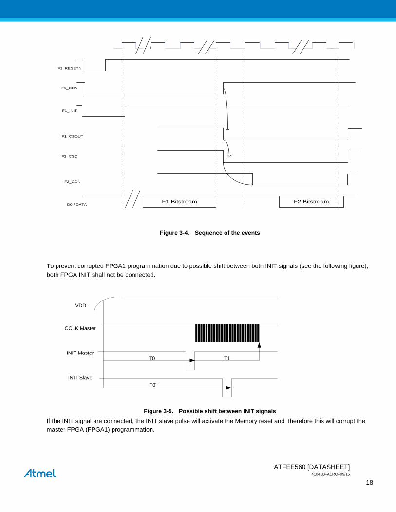
Figure 3-4. Sequence of the events
To prevent corrupted FPGA1 programmation due to possible shift between both INIT signals (see the following figure),
both FPGA INIT shall not be connected.
VDD
CCLK Master
INIT Master
INIT Slave
T0
T0'
T1
Figure 3-5. Possible shift between INIT signals
If the INIT signal are connected, the INIT slave pulse will activate the Memory reset and therefore this will corrupt the
master FPGA (FPGA1) programmation.

ATFEE560 [DATASHEET] 41041BAERO09/15
19
3.3.2 FPGA1 slave – FPGA2 slave
Table 3-2. Configuration mde selection
FPGA1 FPGA2
M0 1 1
M1 0 0
M2 0 0
CCLK input input
Figure 3-6. ATFEE560 connections overview
Both FPGA are in slave, the configuration is always initiated by an other device. This external component will provide
mainly CCLK/CLK and will manage both CS0 signals to select The FPGA to configure.
Bitstream in the memory will be a concatenation of both FPGA bitstream. This concatenation will be built based on the
CS0 management.

ATFEE560 [DATASHEET] 41041BAERO09/15
20
4. Ordering Information
4.1 ATFEE560FF Ordering Codes
Atmel Ordering Code Package
Type
Temperature Range Quality Level
ATFEE560FF-ZB-E CQFP352 25°C Engineering Samples
ATFEE560FF-ZB-SV (1) CQFP352 -55°C / +125°C QMLV equivalent
ATFEE560FF-ZB-MQ (1) CQFP352 -55°C / +125°C QMLQ equivalent
Notes: 1. QML Part Number pending DLA certification
4.2 ATFEE560 Evaluation Kit Ordering Codes
Atmel Ordering Code Description
ATFEE560-EK Evaluation Kit for ATFEE560

ATFEE560 [DATASHEET] 41041BAERO09/15
21
5. Revision History
Doc. Rev. Date Comments
41041A 11/2014 Initial document release
41041B 09/2015 [Features]:
- Radiation data updated
[LVDS]:
- Missing IOs added
[JTAG]:
- JTAG chapter added to the PINOUT description
[Ordering information]:
- Part numbers updated

ATFEE560 [DATASHEET] 41041BAERO09/15
22
Atmel Corporation
1600 Technology Drive
San Jose, CA 95110
USA
Tel: (+1)(408) 441-0311
Fax: (+1)(408) 487-2600
www.atmel.com
Atmel Asia Limited
Unit 01-5 & 16, 19F
BEA Tower, Millennium City 5
418 Kwun Tong Road
Kwun Tong, Kowloon
HONG KONG
Tel: (+852) 2245-6100
Fax: (+852) 2722-1369
Atmel Munich GmbH
Business Campus
Parkring 4
D-85748 Garching b. Munich
GERMANY
Tel: (+49) 89-31970-0
Fax: (+49) 89-3194621
Atmel Japan G.K.
16F Shin-Osaki Kangyo Bldg.
1-6-4 Osaki, Shinagawa-ku
Tokyo 141-0032
JAPAN
Tel: (+81)(3) 6417-0300
Fax: (+81)(3) 6417-0370
© 2012 Atmel Corporation. All rights reserved. / Rev.: 41041BAERO09/15
Atmel®, Atmel logo and combinations thereof, Enabling Unlimited Possibilities®, and others are registered trademarks or trademarks of Atmel Corporation or its
subsidiaries. Other terms and product names may be trademarks of others.
Disclaimer: The information in this document is provided in connection with Atmel products. No license, express or implied, by estoppel or otherwise, to any intellectual property right is granted by this document or in connection with the sale of Atmel products. EXCEPT AS SET FORTH IN THE ATMEL TERMS AND CONDITIONS OF SALES LOCATED ON THE ATMEL WEBSITE, ATMEL ASSUMES NO LIABILITY WHATSOEVER AND DISCLAIMS ANY EXPRESS, IMPLIED OR STATUTORY WARRANTY RELATING TO ITS PRODUCTS INCLUDING, BUT NOT LIMITED TO, THE IMPLIED WARRANTY OF MERCHANTABILITY, FITNESS FOR A PARTICULAR PURPOSE, OR NON-INFRINGEMENT. IN NO EVENT SHALL ATMEL BE LIABLE FOR ANY DIRECT, INDIRECT, CONSEQUENTIAL, PUNITIVE, SPECIAL OR INCIDENTAL DAMAGES (INCLUDING, WITHOUT LIMITATION, DAMAGES FOR LOSS AND PROFITS, BUSINESS INTERRUPTION, OR LOSS OF INFORMATION) ARISING OUT OF THE USE OR INABILITY TO USE THIS DOCUMENT, EVEN IF ATMEL HAS BEEN ADVISED OF THE POSSIBILITY OF SUCH DAMAGES. Atmel makes no representations or warranties with respect to the accuracy or completeness of the contents of this document and reserves the right to make changes to specifications and products descriptions at any time without notice. Atmel does not make any commitment to update the information contained herein. Unless specifically provided otherwise, Atmel products are not suitable for, and shall not be used in, automotive applications. Atmel products are not intended, authorized, or warranted for use as components in applications intended to support or sustain life.