Embed Size (px)
Citation preview

CMOS Generic 24-PinReprogrammable Logic Device
PLDC20G10B/PLDC20G10
Cypress Semiconductor Corporation • 3901 North First Street • San Jose • CA 95134 • 408-943-2600Document #: 38-03010 Rev. ** Revised March 26, 1997
Features
• Fast— Commercial: tPD = 15 ns, tCO = 10 ns, tS = 12 ns
— Military: tPD = 20 ns, tCO = 15 ns, tS = 15 ns• Low power
— ICC max.: 70 mA, commercial
— ICC max.: 100 mA, military• Commercial and military temperature range• User-programmable output cells
— Selectable for registered or combinatorial operation
— Output polarity control
— Output enable source selectable from pin 13 or prod-uct term
• Generic architecture to replace standard logic func-tions including: 20L10, 20L8, 20R8, 20R6, 20R4, 12L10, 14L8, 16L6, 18L4, 20L2, and 20V8
• Eight product terms and one OE product term per out-put
• CMOS EPROM technology for reprogrammability• Highly reliable
— Uses proven EPROM technology
— Fully AC and DC tested
— Security feature prevents logic pattern duplication
— ±10% power supply voltage and higher noise immu-nity
Functional Description
Cypress PLD devices are high-speed electrically programma-ble logic devices. These devices utilize the sum-of-products(AND-OR) structure providing users the ability to program cus-tom logic functions for unique requirements.
In an unprogrammed state the AND gates are connected viaEPROM cells to both the true and complement of every input.By selectively programming the EPROM cells, AND gates maybe connected to either the true or complement or disconnectedfrom both true and complement inputs.
Note:1. The CG7C323 is the PLDC20G10 packaged in the JEDEC-compatible 28-pin PLCC pinout. Pin function and pin order is identical for both PLCC pinouts.
The difference is in the location of the “no connect” or NC pins.
Logic Block Diagram
Pin Configurations 20G10–1
8
9 8 7 6 5 4 3 2 110
15 16 17 18 19 20 21 22 23 24
PROGRAMMABLEANDARRAY
I I I I I I I I CP/I
OUTPUTCELL
8
OUTPUTCELL
8
OUTPUTCELL
OE
OE
OE
8 OE
OUTPUTCELL
8 OE
OUTPUTCELL
8 OE
OUTPUTCELL
8 OE
OUTPUTCELL
8 OE
OUTPUTCELL
V CC
1112
13 14
IVSS
I/OE
8
OUTPUTCELL
8
OUTPUTCELL
I
I/O 9 I/O 8 I/O 7 I/O 6 I/O 5 I/O 4 I/O 3 I/O 2 I/O 1 I/O 0
567891011
4 3 2 282726
12131415161718
25242322212019
III
II
NC
25242322212019
567891011
121314 1516 1718
4 3 2 2827 26
III
III
NC
9
I I V I/O I/O8
I/OI/OV
II
SS
I I CP
/I
V I/O I/O
0 1 0 1
CC C
C9 8
I/OI/OV
II
SS
1 1
CP
/I
NC
20G10–2 20G10–3
I
I/O 2I/O 3I/O4I/O5I/O 6I/O 7
NC
I/OE
NC
PLDC20G10PLDC20G10B
25242322212019
567891011
121314 1516 1718
4 3 2 2827 26
NCII
II
NC
I I CP
/I
V I/O I/O0 1
CC
9 8I/OI/O
II
1
V SS
20G10–4
I
NC
II/O
E
I/O 2I/O3I/O 4I/O5I/O 6I/O7NC
JEDEC PLCCTop View
STD PLCCTop View
LCCTop View
I/O2I/O3I/O4
I/O5I/O 6I/O 7
NC
NC
I/OE
PLDC20G10PLDC20G10B
CG7C323–ACG7C323B–ANC
[1]

PLDC20G10B/PLDC20G10
Document #: 38-03010 Rev. ** Page 2 of 13
Functional Description (continued)
Cypress PLDC20G10 uses an advanced 0.8-micron CMOStechnology and a proven EPROM cell as the programmableelement. This technology and the inherent advantage of beingable to program and erase each cell enhances the reliabilityand testability of the circuit. This reduces the burden on thecustomer to test and to handle rejects.
A preload function allows the registered outputs to be presetto any pattern during testing. Preload is important for testingthe functionality of the Cypress PLD device.
20G10 Functional Description
The PLDC20G10 is a generic 24-pin device that can be pro-grammed to logic functions that include but are not limited to:20L10, 20L8, 20R8, 20R6, 20R4, 12L10, 14L8, 16L6, 18L4,20L2, and 20V8. Thus, the PLDC20G10 provides significantdesign, inventory and programming flexibility over dedicated24-pin devices. It is executed in a 24-pin 300-mil molded DIPand a 300-mil windowed cerDIP. It provides up to 22 inputs and10 outputs. When the windowed cerDIP is exposed to UV light,the 20G10 is erased and then can be reprogrammed.
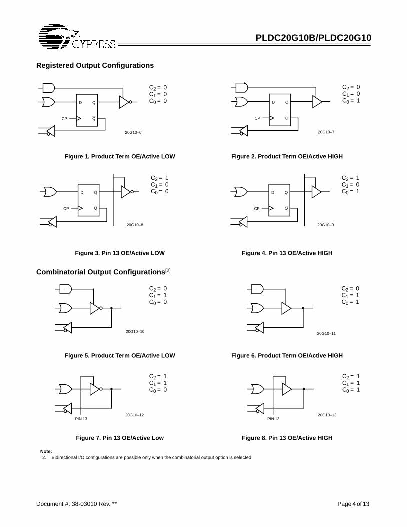
The programmable output cell provides the capability of defin-ing the architecture of each output individually. Each of the 10output cells may be configured with registered or combinatorialoutputs, active HIGH or active LOW outputs, and product termor Pin 13 generated output enables. Three architecture bitsdetermine the configurations as shown in the Configuration
Table and in Figures 1 through 8. A total of eight different con-figurations are possible, with the two most common shown inFigure 3 and Figure 5. The default or unprogrammed state isregistered/active/LOW/Pin 11 OE. The entire programmableoutput cell is shown in the next section.
The architecture bit ‘C1’ controls the registered/combinatorialoption. In either combinatorial or registered configuration, theoutput can serve as an I/O pin, or if the output is disabled, asan input only. Any unused inputs should be tied to ground. Ineither registered or combinatorial configuration, the output ofthe register is fed back to the array. This allows the creation ofcontrol-state machines by providing the next state. The regis-ter is clocked by the signal from Pin 1. The register is initializedon power up to Q output LOW and Q output HIGH.
In both the combinatorial and registered configurations, thesource of the output enable signal can be individually chosenwith architecture bit ‘C2’. The OE signal may be generatedwithin the array, or from the external OE (Pin 13). The Pin 13allows direct control of the outputs, hence having faster en-able/disable times.
Each output cell can be configured for output polarity. The out-put can be either active HIGH or active LOW. This option iscontrolled by architecture bit ‘C0’.
Along with this increase in functional density, the CypressPLDC20G10 provides lower-power operation through the useof CMOS technology and increased testability with a registerpreload feature.
Selection Guide
ICC (mA) tPD (ns) tS (ns) tCO (ns)
GenericPart Number Com/Ind Mil Com/Ind Mil Com/Ind Mil Com/Ind Mil
20G10B–15 70 15 12 10
20G10B–20 70 100 20 20 12 15 12 15
20G10B–25 100 25 18 15
20G10–25 55 25 15 15
20G10–30 80 30 20 20
20G10–35 55 35 30 25
20G10–40 80 40 35 25

PLDC20G10B/PLDC20G10
Document #: 38-03010 Rev. ** Page 3 of 13
Programmable Output Cell
OUTPUTSELECT
MUX
C1 C0Q
QD
CP
INPUT/FEED–BACKMUXC3
C1
20G10–5
01
00
11
10
0
1
C0
C2
OUTPUTENABLE
MUX
C2
PIN 13
OE PRODUCTTERM
Configuration Table
Figure C2 C1 C0 Configuration
1 0 0 0 Product Term OE/Registered/Active LOW
2 0 0 1 Product Term OE/Registered/Active HIGH
5 0 1 0 Product Term OE/Combinatorial/Active LOW
6 0 1 1 Product Term OE/Combinatorial/Active HIGH
3 1 0 0 Pin 13 OE/Registered/Active LOW
4 1 0 1 Pin 13 OE/Registered/Active HIGH
7 1 1 0 Pin 13 OE/Combinatorial/Active LOW
8 1 1 1 Pin 13 OE/Combinatorial/Active HIGH
PLDC20G10B/PLDC20G10
Document #: 38-03010 Rev. ** Page 4 of 13
Registered Output Configurations
Figure 1. Product Term OE/Active LOW Figure 2. Product Term OE/Active HIGH
Figure 3. Pin 13 OE/Active LOW Figure 4. Pin 13 OE/Active HIGH
Q
QD
20G10–6
CP
C2 = 0C1 = 0C0 = 0
Q
QD
20G10–7
CP
C2 = 0C1 = 0C0 = 1
Q
QD
20G10–8
CP
C2 = 1C1 = 0C0 = 0
Q
QD
20G10–9
CP
C2 = 1C1 = 0C0 = 1
Combinatorial Output Configurations[2]
Figure 5. Product Term OE/Active LOW Figure 6. Product Term OE/Active HIGH
Figure 7. Pin 13 OE/Active Low Figure 8. Pin 13 OE/Active HIGH
Note:2. Bidirectional I/O configurations are possible only when the combinatorial output option is selected
20G10–10
C2 = 0C1 = 1C0 = 0
20G10–11
C2 = 0C1 = 1C0 = 1
20G10–12
C2 = 1C1 = 1C0 = 0
20G10–13
C2 = 1C1 = 1C0 = 1
PIN 13 PIN 13

PLDC20G10B/PLDC20G10
Document #: 38-03010 Rev. ** Page 5 of 13
Maximum Ratings
(Above which the useful life may be impaired. For user guide-lines, not tested.)
Storage Temperature .................................–65°C to +150°CAmbient Temperature withPower Applied............................................. –55°C to +125°CSupply Voltage to Ground Potential ............... –0.5V to +7.0V
DC Voltage Applied to Outputsin High Z State ............................................... –0.5V to +7.0V
DC Input Voltage............................................ –3.0V to +7.0V
Output Current into Outputs (LOW) .............................16 mA
DC Programming Voltage PLDC20G10B and CG7C323B–A............................... 13.0V PLDC20G10 and CG7C323–A.................................... 14.0V
Latch-Up Current..................................................... >200 mA
Static Discharge Voltage ............................................. >500V(per MIL-STD-883, Method 8015)
]
Operating Range
RangeAmbient
Temperature VCC
Commercial 0°C to +75°C 5V ±10%
Military[3] –55°C to +125°C 5V ±10%
Industrial –40°C to +85°C 5V ±10%
Electrical Characteristics Over the Operating Range (Unless Otherwise Noted)[4]
Parameter Description Test Conditions Min. Max. Unit
VOH Output HIGH Voltage VCC = Min.,VIN = VIH or VIL
IOH = –3.2 mA Com’l/Ind 2.4 V
IOH = –2 mA Military
VOL Output LOW Voltage VCC = Min.,VIN = VIH or VIL
IOL = 24 mA Com’l/Ind 0.5 V
IOL = 12 mA Military
VIH Input HIGH Level Guaranteed Input Logical HIGH Voltage for All Inputs[5] 2.0 V
VIL Input LOW Level Guaranteed Input Logical LOW Voltage for All Inputs[5] 0.8 V
IIX Input Leakage Current VSS ≤ VIN ≤ VCC –10 +10 µA
ISC Output Short Circuit Current VCC = Max., VOUT = 0.5V[6, 7] –90 mA
ICC Power Supply Current 0 ≤ VIN ≤ VCCVCC = Max., IOUT = 0 mAUnprogrammed Device
Com’l/Ind–15, –20 70 mA
Com’l/Ind–25, –35 55 mA
Military–20, –25 100 mA
Military–30, –40 80 mA
IOZ Output Leakage Current VCC = Max., VSS ≤ VOUT ≤ VCC –100 100 µA
Capacitance[7]
Parameter Description Test Conditions Max. Unit
CIN Input Capacitance TA = 25°C, f = 1 MHz 10 pF
COUT Output Capacitance VIN = 2.0V, VCC = 5.0V 10 pFNotes:3. TA is the “instant on” case temperature.4. See the last page of this specification for Group A subgroup testing information.5. These are absolute values with respect to device ground. All overshoots due to system or tester noise are included.6. Not more than one output should be tested at a time. Duration of the short circuit should not be more than one second. VOUT = 0.5V has been chosen to avoid
test problems caused by tester ground degradation.7. Tested initially and after any design or process changes that may affect these parameters.

PLDC20G10B/PLDC20G10
Document #: 38-03010 Rev. ** Page 6 of 13
AC Test Loads and Waveforms (Commercial)
5V
OUTPUT
INCLUDINGJIG ANDSCOPE
OUTPUT
50pF
2.08V=Vthc OUTPUT 2.13V=V thm
(a) (b)
20G10–14
5V
OUTPUT
INCLUDINGJIG ANDSCOPE
5 pF
20G10–15 20G10–16
R1 238 Ω(319Ω MIL)
R1 238Ω(319Ω MIL)
R2 170Ω(236Ω MIL)
R2 170Ω(236Ω MIL)
Equivalent to: THÉVENIN EQUIVALENT (Commercial) Equivalent to: THÉVENIN EQUIVALENT (Military/Industrial)
99Ω 136 Ω
Switching Characteristics Over Operating Range[3, 8, 9]
Commercial
B–15 B–20 –25 –35
Parameter Description Min. Max. Min. Max. Min. Max. Min. Max. Unit
tPD Input or Feedback to Non-Registered Output 15 20 25 35 ns
tEA Input to Output Enable 15 20 25 35 ns
tER Input to Output Disable 15 20 25 35 ns
tPZX Pin 11 to Output Enable 12 15 20 25 ns
tPXZ Pin 11 to Output Disable 12 15 20 25 ns
tCO Clock to Output 10 12 15 25 ns
tS Input or Feedback Set-Up Time 12 12 15 30 ns
tH Hold Time 0 0 0 0 ns
tP[10] Clock Period 22 24 30 55 ns
tWH Clock High Time 8 10 12 17 ns
tWL Clock Low Time 8 10 12 17 ns
fMAX[11] Maximum Frequency 45.4 41.6 33.3 18.1 MHz
Notes:8. Part (a) of AC Test Loads and Waveforms used for all parameters except tER, tPZX, and tPXZ. Part (b) of AC Test Loads and Waveforms used for tER, tPZX,
and tPXZ.9. The parameters tER and tPXZ are measured as the delay from the input disable logic threshold transition to VOH – 0.5V for an enabled HIGH output or VOL
+ 0.5V for an enabled LOW input.10. tP, minimum guaranteed clock period is that guaranteed for state machine operation and is calculated from tP = tS + tCO. The minimum guaranteed period
for registered data path operation (no feedback) can be calculated as the greater of (tWH + tWL) or (tS + tH).11. fMAX, minimum guaranteed operating frequency, is that guaranteed for state machine operation and is calculated from fMAX = 1/(tS + tCO). The minimum
guaranteed fMAX for registered data path operation (no feedback) can be calculated as the lower of 1/(tWH + tWL) or 1/(tS + tH).

PLDC20G10B/PLDC20G10
Document #: 38-03010 Rev. ** Page 7 of 13
Switching Characteristics Over Operating Range[3, 8, 9] (continued)
Military/Industrial
B–20 B–25 –30 –40
Parameter Description Min. Max. Min. Max. Min. Max. Min. Max. Unit
tPD Input or Feedback to Non-Registered Output 20 25 30 40 ns
tEA Input to Output Enable 20 25 30 40 ns
tER Input to Output Disable 20 25 30 40 ns
tPZX Pin 11 to Output Enable 17 20 25 25 ns
tPXZ Pin 11 to Output Disable
17 20 25 25 ns
tCO Clock to Output 15 15 20 25 ns
tS Input or Feedback Set-Up Time
15 18 20 35 ns
tH Hold Time 0 0 0 0 ns
tP[10] Clock Period 30 33 40 60 ns
tWH Clock High Time 12 14 16 22 ns
tWL Clock Low Time 12 14 16 22 ns
fMAX[11] Maximum Frequency 33.3 30.3 25.0 16.6 MHz
Switching Waveform
t EAtPD
INPUTS I/O,
tH
REGISTEREDFEEDBACK
CP
REGISTEREDOUTPUTS
COMBINATORIALOUTPUTS
20G10–17
tS
tPXZ
tER
tCO
tW tW
OE
tP
tPZX

PLDC20G10B/PLDC20G10
Document #: 38-03010 Rev. ** Page 8 of 13
Functional Logic Diagram
01
2
3
4
5
6
7
8
9
10
11
23
22
21
20
19
18
17
16
15
14
13
16 20 24 28 32 36 40
OE0
7
•••
1284
OE0
7
•••
OE0
7
•••
OE0
7
•••
OE0
7
•••
OE0
7
•••
OE0
7
•••
OE0
7
•••
OE0
7
•••
OE0
7
•••
OUTPUTCELL
OUTPUTCELL
OUTPUTCELL
OUTPUTCELL
OUTPUTCELL
OUTPUTCELL
OUTPUTCELL
OUTPUTCELL
OUTPUTCELL
OUTPUTCELL

PLDC20G10B/PLDC20G10
Document #: 38-03010 Rev. ** Page 9 of 13
MILITARY SPECIFICATIONSGroup A Subgroup Testing
Ordering Information
tPD(ns)
tS(ns)
tCO(ns)
ICC(mA) Ordering Code
Package Name Package Type
Operating Range
15 12 10 70 PLDC20G10B–15PC P13 24-Lead (300-Mil) Molded DIP Commercial
PLDC20G10B–15WC W14 24-Lead (300-Mil) Windowed CerDIP
20 15 15 100 PLDC20G10B–20DMB D14 24-Lead (300-Mil) CerDIP Military
25 15 15 55 PLDC20G10–25JC J64 28-Lead Plastic Leaded Chip Carrier Commercial
PLDC20G10–25PC/PI P13 24-Lead (300-Mil) Molded DIP Commercial/Industrial
PLDC20G10–25WC W14 24-Lead (300-Mil) Windowed CerDIP Commercial
30 20 20 80 PLDC20G10–30DMB D14 24-Lead (300-Mil) CerDIP Military
PLDC20G10–30LMB L64 28-Square Leadless Chip Carrier
PLDC20G10–30WMB W14 24-Lead (300-Mil) Windowed CerDIP
35 30 25 55 PLDC20G10–35JC J64 28-Lead Plastic Leaded Chip Carrier Commercial
PLDC20G10–35PC P13 24-Lead (300-Mil) Molded DIP
DC Characteristics
Parameter Subgroups
VOH 1, 2, 3
VOL 1, 2, 3
VIH 1, 2, 3
VIL 1, 2, 3
IIX 1, 2, 3
IOZ 1, 2, 3
ICC 1, 2, 3
Switching Characteristics
Parameter Subgroups
tPD 9, 10, 11
tPZX 9, 10, 11
tCO 9, 10, 11
tS 9, 10, 11
tH 9, 10, 11

PLDC20G10B/PLDC20G10
Document #: 38-03010 Rev. ** Page 10 of 13
Package Diagrams
24-Lead (300-Mil) CerDIP D14MIL–STD–1835 D– 9Config.A
28-Lead Plastic Leaded Chip Carrier J64
28-Square Leadless Chip Carrier L64MIL–STD–1835 C–4

PLDC20G10B/PLDC20G10
Document #: 38-03010 Rev. ** Page 11 of 13
Package Diagrams (continued)
28-Pin Windowed Leaded Chip Carrier H64

PLDC20G10B/PLDC20G10
Document #: 38-03010 Rev. ** Page 12 of 13
Package Diagrams (continued)
24-Lead (300-Mil) Molded DIP P13/P13A
24-Lead (300-Mil) Windowed CerDIP W14MIL–STD–1835 D– 9Config.A

PLDC20G10B/PLDC20G10
Document #: 38-03010 Rev. ** Page 13 of 13 © Cypress Semiconductor Corporation, 1997. The information contained herein is subject to change without notice. Cypress Semiconductor Corporation assumes no responsibility for the useof any circuitry other than circuitry embodied in a Cypress Semiconductor product. Nor does it convey or imply any license under patent or other rights. Cypress Semiconductor does not authorizeits products for use as critical components in life-support systems where a malfunction or failure may reasonably be expected to result in significant injury to the user. The inclusion of CypressSemiconductor products in life-support systems application implies that the manufacturer assumes all risk of such use and in doing so indemnifies Cypress Semiconductor against all charges.
Document Title: PLDC20G10B/PLDC20G10 CMOS Generic 24-Pin Reprogrammable Logic DeviceDocument Number: 38-03010
REV. ECN NO. Issue Date Orig. of Change Description of Change
** 106292 04/25/01 SZV Change from Spec number: 38-00019 to 38-03010