Embed Size (px)
Citation preview
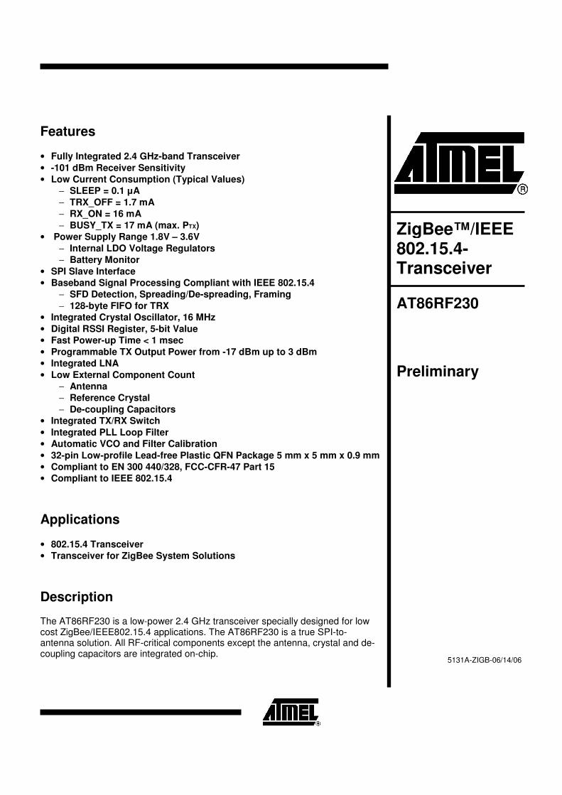
ZigBee™/IEEE 802.15.4-Transceiver
AT86RF230
Preliminary
5131A-ZIGB-06/14/06
Features
• Fully Integrated 2.4 GHz-band Transceiver
• -101 dBm Receiver Sensitivity
• Low Current Consumption (Typical Values)
− SLEEP = 0.1 µA
− TRX_OFF = 1.7 mA
− RX_ON = 16 mA
− BUSY_TX = 17 mA (max. PTX)
• Power Supply Range 1.8V – 3.6V
− Internal LDO Voltage Regulators
− Battery Monitor
• SPI Slave Interface
• Baseband Signal Processing Compliant with IEEE 802.15.4
− SFD Detection, Spreading/De-spreading, Framing
− 128-byte FIFO for TRX
• Integrated Crystal Oscillator, 16 MHz
• Digital RSSI Register, 5-bit Value
• Fast Power-up Time < 1 msec
• Programmable TX Output Power from -17 dBm up to 3 dBm
• Integrated LNA
• Low External Component Count
− Antenna
− Reference Crystal
− De-coupling Capacitors
• Integrated TX/RX Switch
• Integrated PLL Loop Filter
• Automatic VCO and Filter Calibration
• 32-pin Low-profile Lead-free Plastic QFN Package 5 mm x 5 mm x 0.9 mm
• Compliant to EN 300 440/328, FCC-CFR-47 Part 15
• Compliant to IEEE 802.15.4
Applications
• 802.15.4 Transceiver
• Transceiver for ZigBee System Solutions
Description
The AT86RF230 is a low-power 2.4 GHz transceiver specially designed for low cost ZigBee/IEEE802.15.4 applications. The AT86RF230 is a true SPI-to-antenna solution. All RF-critical components except the antenna, crystal and de-coupling capacitors are integrated on-chip.

2 AT86RF230 [Preliminary] 5131A-ZIGB-06/14/06
Table of contents
1. Abbreviations ...................................................................................................................................................4 2. General Circuit Description..............................................................................................................................5 3. Technical Parameters......................................................................................................................................6
3.1. Absolute Maximum Ratings.........................................................................................................................6 3.2. Recommended Operating Range................................................................................................................6 3.3. Digital Pin Specifications .............................................................................................................................6 3.4. General RF Specifications...........................................................................................................................7 3.5. Transmitter Specifications ...........................................................................................................................7 3.6. Receiver Specifications ...............................................................................................................................8 3.7. Current Consumption Specifications...........................................................................................................9 3.8. SPI Timing Specifications............................................................................................................................9 3.9. Crystal Parameter Specifications ..............................................................................................................10
4. Basic Operating Modes .................................................................................................................................11 4.1. Configuration .............................................................................................................................................11 4.2. Basic Operating Mode Description............................................................................................................12
4.2.1. P_ON ....................................................................................................................................................12 4.2.2. SLEEP...................................................................................................................................................12 4.2.3. TRX_OFF..............................................................................................................................................12 4.2.4. PLL_ON ................................................................................................................................................12 4.2.5. RX_ON and BUSY_RX.........................................................................................................................13 4.2.6. RX_ON_NOCLK ...................................................................................................................................13 4.2.7. BUSY_TX..............................................................................................................................................13
4.3. Basic Mode Timing....................................................................................................................................13 4.3.1. Wake-up Procedure ..............................................................................................................................13 4.3.2. Transition from PLL_ON via BUSY_TX to RX_ON...............................................................................14 4.3.3. State Transition Timing .........................................................................................................................15
5. Extended Operating Modes ...........................................................................................................................16 5.1. Peer-to-peer Network Support ..................................................................................................................16 5.2. Configuration .............................................................................................................................................18 5.3. Extended Operation Mode Description .....................................................................................................18
5.3.1. RX_AACK_ON ......................................................................................................................................18 5.3.2. TX_ARET_ON.......................................................................................................................................18 5.3.3. RX_AACK_NOCLK...............................................................................................................................19
6. Functional Description ...................................................................................................................................20 6.1. RSSI/Energy Detection .............................................................................................................................20 6.2. Link Quality Indication ...............................................................................................................................20 6.3. Clear Channel Assessment.......................................................................................................................20 6.4. Voltage Regulators ....................................................................................................................................20 6.5. Battery Monitor ..........................................................................................................................................21 6.6. Crystal Oscillator .......................................................................................................................................22 6.7. PLL Frequency Synthesizer ......................................................................................................................23 6.8. Automatic Filter Tuning .............................................................................................................................24
7. PHY to Micro-Controller Interface..................................................................................................................25 7.1. SPI Protocol...............................................................................................................................................25 7.2. Register Access Mode (Short Mode) ........................................................................................................26 7.3. Frame Buffer Access Modes (Long Modes)..............................................................................................27 7.4. Frame Receive Procedure ........................................................................................................................28 7.5. Frame Transmit Procedure .......................................................................................................................28 7.6. Sleep/Wake-up and Transmit Signal.........................................................................................................29 7.7. Interrupt Logic............................................................................................................................................30

3
AT86RF230 [Preliminary]
5131A-ZIGB-06/14/06
8. Control Registers ...........................................................................................................................................31 9. Application Circuit ..........................................................................................................................................42 10. Pin Configuration ...........................................................................................................................................44
10.1. Pin-out Diagram.........................................................................................................................................45 10.2. Decoupling.................................................................................................................................................45 10.3. Analog Pins ...............................................................................................................................................45 10.4. RF Pins......................................................................................................................................................45 10.5. Digital Pins.................................................................................................................................................46
11. Ordering Information......................................................................................................................................47 12. Soldering Information.....................................................................................................................................47 13. Package Thermal Properties .........................................................................................................................47 14. Package Drawing – 32QN1 ...........................................................................................................................48 15. References.....................................................................................................................................................49 16. Revisions .......................................................................................................................................................49

4 AT86RF230 [Preliminary] 5131A-ZIGB-06/14/06
1. Abbreviations
AACK — Auto acknowledge ACK — Acknowledge ADC — Analog-to-digital converter AGC — Automatic gain control ARET — Auto retry AVREG — Analog voltage regulator BATMON — Battery monitor BBP — Base-band processor BPF — Complex band-pass filter CCA — Clear channel assessment CLKM — Clock main CRC — Cyclic redundancy check CSMA — Carrier sense multiple access DCLK — Digital clock DCU — Delay calibration unit DVREG — Digital voltage regulator ED — Energy detection ESD — Electro static discharge EVM — Error vector magnitude FIFO — First in first out FTN — Automatic filter tuning GPIO — General purpose input output LDO — Low-drop output LNA — Low-noise amplifier LO — Local oscillator LQI — Link-quality indication LSB — Least significant bit MSB — Most significant bit MSK — Minimum shift keying O-QPSK — Offset-quadrature phase shift keying PA — Power amplifier PAN — Personal area network PER — Packet error rate PHY — Physical layer PLL — Phase-locked loop POR — Power-on reset PPF — Poly-phase filter PSDU — PHY service data unit QFN — Quad flat no-lead package RF — Radio frequency RSSI — Received signal strength indicator RX — Receiver SFD — Start frame delimiter SPI — Serial peripheral interface SRAM — Static random access memory TX — Transmitter VCO — Voltage controlled oscillator VREG — Voltage regulator XOSC — Crystal oscillator

5
AT86RF230 [Preliminary]
5131A-ZIGB-06/14/06
2. General Circuit Description
LNA PPF ADC
AGC
PAFrequency Synthesis
I
Q
FTNAVREG
BATMON
SPISlave
Interface
TX powercontrol
TX Data
Limiter
5
RSSI
XOSC
Control Logic/Configuration
Registers
CLKM
XT
AL1
XT
AL2
TRX Data Buffer
TX BBP
RX BBPBPF
IRQ
SEL
SCLK
MISO
MOSI
SLP_TR
RSTN
DCLK
RFP
RFN
Digital DomainAnalog Domain
DVREG
Figure 2-1. Block Diagram of AT86RF230
This single-chip RF transceiver provides a complete radio interface between the antenna and the micro-controller. It comprises the analog radio part, digital demodulation including time and frequency synchronization and data buffering. The number of external components is minimized so that only the antenna, the crystal and four decoupling capacitors are required. The bidirectional differential antenna pins are used in common for RX and TX, so no external antenna switch is needed.
The transceiver block diagram is shown in Figure 2-1. The receiver path is based on a low-IF topology. The channel filter consists of three single side-band active RC resonators forming a 2 MHz band-pass filter with a Butterworth characteristic centered at 2 MHz. Two 1
st-order high-pass filters were added to the signal path to
achieve capacitive coupling at the single side-band filter (SSBF) output to suppress DC offset and integrator feedback at the limiter amplifier. The 3-stage limiter amplifier provides sufficient gain to overcome the DC offset of the succeeding single channel ADC and generates a digital RSSI signal with 3 dB granularity. The low-IF signal is sampled at 16 MHz with 1-bit resolution and applied to the digital signal processing part.
Direct VCO modulation is used to generate the transmit signal. The modulation scheme is offset-QPSK (O-QPSK) with half-sine pulse shaping and 32-length block coding (spreading). This is equivalent to minimum shift keying (MSK) when transforming the spreading code sequences appropriately. The modulation signal is applied to both the VCO and the fractional-N PLL to ensure the coherent phase modulation required for demodulation as an O-QPSK signal. The frequency-modulated LO signal is fed to the power amplifier.
Two on-chip low-dropout voltage regulators provide the analog and digital 1.8V supply. The SPI interface and the control registers will retain their settings in SLEEP mode when the regulators are turned off. The RX and TX signal processing paths are highly integrated and optimized for low power consumption.

6 AT86RF230 [Preliminary] 5131A-ZIGB-06/14/06
3. Technical Parameters
3.1. Absolute Maximum Ratings Note: Stresses beyond those listed under “Absolute Maximum Ratings” may cause permanent damage to the device. This is a stress rating only and functional operation of the device at these or any other conditions beyond those indicated in the operational sections of this specifications is not implied. Exposure to absolute maximum rating conditions for extended periods may affect device reliability.
No Parameter Symbol Min Typ Max Unit Conditions/Notes
3.1.1 Storage temperature Tstor -50 150 °C
3.1.2 Lead temperature Tlead 260 °C T = 10s (soldering profile compliant with IPC/JEDEC J-STD-020B)
3.1.3 ESD-protection VESD 2 200 500
kV V V
Compl. to [2], passed 4 kV Compl. to [3], Compl. to [4], passed 750V
3.1.4 Input RF level PRF +10 dBm
3.1.5 Voltage on all pins (except pins 13, 14, 29)
-0.3 Vdd+0.3
≤ 3.6
V
3.1.6 Voltage on pins 13, 14, 29 -0.3 2 V
Table 3-1. Absolute Maximum Ratings
3.2. Recommended Operating Range
No Parameter Symbol Min Typ Max Unit Conditions/Notes
3.2.1 Operating temperature range Top -40 +85 °C
3.2.2 Supply voltage Vdd 1.8 3.6 V
Table 3-2. Operating Range
3.3. Digital Pin Specifications Test Conditions (unless otherwise stated): Tamb = 25°C
No Parameter Symbol Min Typ Max Unit Conditions/Notes
3.3.1 High level input voltage VIH Vdd – 0.4 V
3.3.2 Low level input voltage VIL 0.4 V
3.3.3 High level output voltage VOH Vdd – 0.4 V For all output current loads defined in register TRX_CTR_0
3.3.4 Low level output voltage VOL 0.4 V For all output current loads defined in register TRX_CTR_0

7
AT86RF230 [Preliminary]
5131A-ZIGB-06/14/06
No Parameter Symbol Min Typ Max Unit Conditions/Notes
3.3.5 Controller clock frequency (CLKM)
fCLKM 0 1 2 4 8
16
MHz MHz MHz MHz MHz MHz
Programmable in register TRX_CTRL_0
Table 3-3. Digital Pin Specifications
The capacitive load should not be larger than 50 pF for all I/Os when using the default driver strength settings. Generally, large load capacitances will increase the overall current consumption.
3.4. General RF Specifications Test Conditions (unless otherwise stated): Vdd = 3V, f = 2.45 GHz, Tamb = 25°C, Measurement setup see Figure 9-1
No Parameter Symbol Min Typ Max Unit Conditions/Notes
3.4.1 Frequency range f 2405 2480 MHz
3.4.2 Bit rate fbit 250 kbit/s As specified in [1]
3.4.3 Chip rate fchip 2000 kchip/s As specified in [1]
3.4.4 Reference oscillator frequency
fclk 16 MHz
3.4.5 Reference oscillator settling time
0.5 1 ms Leaving SLEEP state to clock available at pin CLKM
3.4.6 Reference frequency accuracy for correct functionality
-60 +60 ppm ±40 ppm is required by [1]
3.4.7 20 dB bandwidth B20dB 2.8 MHz
Table 3-4: General RF Parameters
3.5. Transmitter Specifications Test Conditions (unless otherwise stated): Vdd = 3V, f = 2.45 GHz, Tamb = 25°C, Measurement setup see Figure 9-1
No Parameter Symbol Min Typ Max Unit Conditions/Notes
3.5.1 Nominal output power PTX 0 3 6 dBm Max. value
3.5.2 Output power range 20 dB 16 steps (register PHY_TX_PWR)
3.5.3 Output power accuracy ±3 dB
3.5.4 TX Return loss 10 dB 100Ω differential impedance, PTX = 3 dBm
3.5.5 EVM 8 %rms Channel number = 20
3.5.6 Harmonics 2nd harmonic 3rd harmonic
-38 -45
dBm dBm

8 AT86RF230 [Preliminary] 5131A-ZIGB-06/14/06
No Parameter Symbol Min Typ Max Unit Conditions/Notes
3.5.7 Spurious emissions
30 – ≤1000 MHz >1 – 12.75 GHz 1.8 – 1.9 GHz 5.15 – 5.3 GHz
-36 -30 -47 -47
dBm dBm dBm dBm
Complies with EN 300 440, FCC-CFR-47 part 15, ARIB STD-66, RSS-210
Table 3-5. TX Parameters
3.6. Receiver Specifications
Test Conditions (unless otherwise stated): Vdd = 3V, f = 2.45 GHz, Tamb = 25°C, Measurement setup see Figure 9-1
No Parameter Symbol Min Typ Max Unit Conditions/Notes
3.6.1 Receiver sensitivity -101 dBm AWGN channel, PER≤1%, PSDU length of 20 octets
3.6.2 Return loss 10 dB 100Ω differential impedance
3.6.3 Noise figure NF 6 dB
3.6.4 Maximum RX input level 10 dBm PER ≤ 1%, PSDU length of 20 octets
3.6.5 Adjacent channel rejection -5 MHz
34 dBm PER ≤ 1%, PSDU length of 20 octets, PRF = -82 dBm
3.6.6 Adjacent channel rejection +5 MHz
36 dBm PER ≤ 1%, PSDU length of 20 octets, PRF = -82 dBm
3.6.7 Alternate adjacent channel rejection -10 MHz
52 dBm PER ≤ 1%, PSDU length of 20 octets, PRF = -82 dBm
3.6.8 Alternate adjacent channel rejection +10 MHz
53 dBm PER ≤ 1%, PSDU length of 20 octets, PRF = -82 dBm
3.6.9 Spurious emissions LO leakage 30 – 1000 MHz 1 – 12.75 GHz
-75
-57 -47
dBm dBm dBm
3.6.10 TX/RX carrier frequency offset
-300 300 kHz Sensitivity loss < 2 dB
3.6.11 3rd
-order intercept point IIP3 -9 dB At maximum gain Offset freq. interf. 1 = 5 MHz Offset freq. interf. 2 = 10 MHz
3.6.12 2nd
-order intercept point IIP2 24 dB At maximum gain Offset freq. interf. 1 = 60 MHz Offset freq. interf. 2 = 62 MHz
3.6.13 RSSI accuracy absolute -5 5 dB Tolerance within gain step
3.6.14 RSSI dynamic range 84 dB
3.6.15 RSSI resolution 3 dB
3.6.16 Minimum RSSI value 0 PRF < -91 dBm
3.6.17 Maximum RSSI value 28 PRF > -10 dBm
Table 3-6. RX Parameters

9
AT86RF230 [Preliminary]
5131A-ZIGB-06/14/06
3.7. Current Consumption Specifications Test Conditions (unless otherwise stated): Vdd = 3V, Tamb = 25°C, CLKM = OFF, Measurement setup see Figure 9-1
No Parameter Symbol Min Typ Max Unit Conditions/Notes
3.7.1 Supply current transmit mode IBUSY_TX 17 15 13 10
mA mA mA mA
PTX = 3 dBm PTX = 1 dBm PTX = -3 dBm PTX = -17 dBm (the current consumption will be reduced by approx. 2 mA at Vdd = 1.8V for each output power level)
3.7.2 Supply current receive mode IRX_ON 16 mA State: RX_ON
3.7.3 Supply current TRX_OFF mode
ITRX_OFF 1.7 mA State: TRX_OFF
3.7.4 Supply current SLEEP mode ISLEEP 0.1 µA State: SLEEP
Table 3-7. Current Consumption
3.8. SPI Timing Specifications Test Conditions (unless otherwise stated): Vdd = 3V, Tamb = 25°C
No Parameter Symbol Min Typ Max Unit Conditions/Notes
3.8.1 SCLK frequency (synchronous)
8 MHz
3.8.2 SCLK frequency (asynchronous)
7.5 MHz
3.8.3 SEL low to MISO active t1 180 ns
3.8.4 SCLK to MISO out t2 48 ns data hold time
3.8.5 MOSI setup time t3 10 ns
3.8.6 MOSI hold time t4 10 ns
3.8.7 LSB last byte to MSB next byte
t5 250 ns
3.8.8 SEL high to MISO tristate t6 10 ns
3.8.9 SLP_TR pulse width t7 65 ns
Table 3-8. SPI Timing Parameters (see Figure 7-2)

10 AT86RF230 [Preliminary] 5131A-ZIGB-06/14/06
3.9. Crystal Parameter Specifications
No Parameter Symbol Min Typ Max Unit Conditions/Notes
3.9.1 Crystal frequency f0 16 MHz
3.9.2 Load capacitance CL 8 14 pF
3.9.3 Static capacitance C0 7 pF
3.9.4 Series resistance R1 100 Ω
Table 3-9. Crystal Parameter Specifications
11
AT86RF230 [Preliminary]
5131A-ZIGB-06/14/06
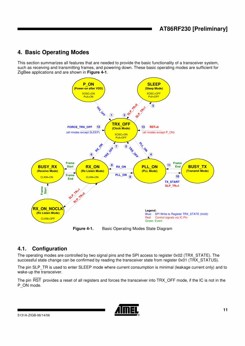
4. Basic Operating Modes
This section summarizes all features that are needed to provide the basic functionality of a transceiver system, such as receiving and transmitting frames, and powering down. These basic operating modes are sufficient for ZigBee applications and are shown in Figure 4-1.
2
TRX_O
FF
SLP_T
R=1
Legend:
Blue: SPI Write to Register TRX_STATE (0x02)
Red: Control signals via IC PinGreen: Event
SLP
_TR=0
PLL
_ON
RX_ON
PLL_ON
TRX_OFF(Clock Mode)
XOSC=ON
Pull=OFF
RX_O
N
P_ON(Power-on after VDD)
XOSC=ON
Pull=ON
SLEEP(Sleep Mode)
XOSC=OFFPull=OFF
(all modes except P_ON)
FORCE_TRX_OFF
(all modes except SLEEP)
Frame
Start
Frame
End
Frame
End BUSY_TX(Transmit Mode)
PLL_ON(PLL Mode)
RX_ON(Rx Listen Mode)
BUSY_RX(Receive Mode)
CLKM=ON
TX_START
SLP_TR=1
TRX_O
FF
TRX_O
FF
1
3
4
57
6
8
9
11
10
RX_ON_NOCLK(Rx Listen Mode)
CLKM=OFF
SLP_TR=1
SLP_TR=0F
ram
e
Sta
rt
CLKM=ON
RST=012 13
Figure 4-1. Basic Operating Modes State Diagram
4.1. Configuration The operating modes are controlled by two signal pins and the SPI access to register 0x02 (TRX_STATE). The successful state change can be confirmed by reading the transceiver state from register 0x01 (TRX_STATUS).
The pin SLP_TR is used to enter SLEEP mode where current consumption is minimal (leakage current only) and to wake-up the transceiver.
The pin RST provides a reset of all registers and forces the transceiver into TRX_OFF mode, if the IC is not in the
P_ON mode.

12 AT86RF230 [Preliminary] 5131A-ZIGB-06/14/06
The state change commands FORCE_TRX_OFF and TRX_OFF both lead to a transition into TRX_OFF state. If the transceiver is in the BUSY_RX or BUSY_TX state, the command FORCE_TRX_OFF interrupts the active receiving or transmitting process, and forces an immediate transition. On the other hand, a TRX_OFF command is stored until a frame currently being received or transmitted is finished. After the end of the frame, the transition to TRX_OFF is performed.
4.2. Basic Operating Mode Description
4.2.1. P_ON
When the external supply voltage (VDD) is first supplied to the transceiver IC, the system is in the P_ON (Power-on) mode. In this mode, the crystal oscillator is activated and the master clock for the controller is provided at the CLKM pin after a delay of 128µs to ensure a steady state of the crystal oscillator.
All digital inputs have pull-up or pull-down resistors (see Table 10-3). This is necessary to support controllers where GPIO signals are undefined after reset. The input pull-up and pull-down resistors are disabled when the transceiver leaves the P_ON state.
A valid SPI write access to the register TRX_STATE with the values TRX_OFF or FORCE_TRX_OFF is necessary to leave the P_ON state.
Prior to leaving P_ON, the controller must set the pins to the default operating values: SLP_TR = 0 and 1RST = .
An on-chip power-on-reset sets the all register to its default values. A dedicated reset signal from the controller at
the pin RST is not necessary, but recommended for HW/SW synchronization reasons.
4.2.2. SLEEP
In SLEEP mode, the entire transceiver IC is disabled. No circuitry is running. The current consumption in this mode is leakage current only. This mode can only be entered from state TRX_OFF, when the pin SLP_TR is set to “1”. There is no way to switch the transceiver to SLEEP mode via SPI register access.
Leaving this state is possible in two ways:
Setting the SLP_TR pin to “0” returns the transceiver to the TRX_OFF mode without resetting any registers. Using
0RST = resets the SPI and configuration registers to their default values and forces the IC into the TRX_OFF
mode.
4.2.3. TRX_OFF
The TRX_OFF mode provides the master clock for the controller in synchronous operation mode, allowing the
software to run without the need for the radio to be powered on. The pins SLP_TR and RST are enabled for mode
control.
In this mode, the SPI interface and crystal oscillator are active. The voltage regulator is enabled and provides 1.8V to the digital core for have access to the frame data buffers.
The transition from P_ON to TRX_OFF mode is described in section 4.2.1.
4.2.4. PLL_ON
Entering the PLL_ON mode from TRX_OFF will first enable the analog voltage regulator. After the voltage regulator has settled, the PLL frequency synthesizer is enabled. When the PLL has settled at the receive frequency, a successful PLL lock is indicated by an interrupt request at the IRQ pin.
During PLL_ON mode, the command RX_ON via register 0x02 (TRX_STATE) sets the transceiver to RX_ON mode, even if the PLL is not yet settled.

13
AT86RF230 [Preliminary]
5131A-ZIGB-06/14/06
4.2.5. RX_ON and BUSY_RX
The RX_ON mode enables the analog and digital receiver blocks and the PLL frequency synthesizer. The transition from TRX_OFF mode to RX_ON mode is started by setting the TRX_STATE to RX_ON via a SPI write access to register 0x02 (TRX_STATE).
The receive mode is internally divided into RX_ON mode and BUSY_RX mode. There is no difference between the modes with respect to the analog radio part. During RX_ON mode, only the preamble detection of the digital signal processing is running. When a preamble is detected, the digital receiver is turned on, switching to the BUSY_RX mode.
SLP_TR = 1 is only evaluated in RX_ON mode. When receiving a frame in BUSY_RX mode, the SLP_TR pin has no effect.
4.2.6. RX_ON_NOCLK
If the radio is listening for an incoming frame and the controller is not running an application, the controller can be powered down to decrease the total system power consumption. This special power-down scenario for controllers running in synchronous mode is supported by the AT86RF230 using the state RX_ON_NOCLK.
This state can only be entered by setting SLP_TR = 1 while the IC is in the RX_ON mode. The CLKM pin will then be disabled 35 clock cycles after the rising edge at the SLP_TR pin. This will enable the controller to complete its power-down sequence. The reception of a frame is signalized to the controller by a RX_START IRQ (see Figure 7-13). The clock CLKM is turned on once again and the transceiver enters the BUSY_RX state.
The end of the transaction is signaled to the controller by an TRX_END interrupt. After the transaction has been completed, the transceiver will enter the RX_ON state. The transceiver will only re-enter the RX_ON_NOCLK state when the SLP_TR has been reset to “0”, and afterwards set to “1” again.
If the transceiver is in the RX_ON_NOCLK state, and the SLP_TR pin is reset to “0”, it will enter the RX _ON state, and it will again start to supply the micro-controller with the clock signal.
4.2.7. BUSY_TX
Transmitting can only be started from PLL_ON mode. There are two ways to start transmitting: using pin SLP_TR = 1 or SPI command TX_START in register 0x02 (TRX_STATE). Either of these will cause the IC to enter BUSY_TX mode.
During the transition to BUSY_TX mode, the PLL frequency shifts 1.5 MHz to enable the different LO frequencies needed between receive and transmit modes. Transmission of the first data chip of the preamble is delayed by 16 µs to allow PLL settling and PA ramping.
When the end of the frame has been transmitted, the IC will automatically turn off the power amplifier and transition from the BUSY_TX mode to the PLL_ON mode. The PLL settles to the receiver LO frequency (-1.5 MHz frequency step).
If the frame transmission was initiated by setting the pin SLP_TR to “1”, a new transmission will only be started when the pin SLP_TR has been reset to “0” and afterwards to set to “1” again.
4.3. Basic Mode Timing The following paragraphs depict the method of switching from one mode to another.
4.3.1. Wake-up Procedure
The wake-up procedure from SLEEP mode is shown in Figure 4-2.
Deasserting the pin SLP_TR enables the crystal oscillator. After approximately 0.3 - 0.5 ms, the internal clock signal is available. After 128 µs the clock signal is delivered at the CLKM pin providing the master clock to the

14 AT86RF230 [Preliminary] 5131A-ZIGB-06/14/06
micro-controller. An additional 256 µs timer ensures that frequency stability is sufficient to drive filter tuning (FTN) and the PLL. After band-gap voltage and digital voltage regulator settling, the transceiver enters the TRX_OFF state and waits for further commands.
0 600500 700
Active Blocks
800 900 1000 1100
FTN BG DVREG AVREG 16 s PLLTimer 256 sTimer 128 s
TRX_OFFState PLL_ON
CommandPLL_ON,RX_ON
SLP_TR=0
XOSC
Timer 128 s
VDD on
XOSC
TRX_OFF
Typical block settling time, stays on
Block active
waiting for SPI commands
P_ON
XOSC deliversclock
CLKM deliversclock
Clock stable
IRQPLL locked
Signals/Events
RX_ON
RX_ONSLEEP
RST=0Pin
CLKM_CTRL
~400
Time [µs]
Time [µs]
µµµµµµµµµµµµ
µµµµ
Figure 4-2. Wake-up Procedure from SLEEP Mode and P_ON Mode to RX_ON Mode (PLL locked)
Forcing PLL_ON mode or RX_ON mode initiates a ramp-up sequence of the analog voltage regulator followed by a 16 µs timer. This timer makes sure that the analog 1.8V supply is stabilized before enabling PLL circuitry. RX_ON mode can be forced any time during PLL_ON mode regardless of the PLL lock signal.
When the wake-up sequence is started from P_ON mode (VDD first applied to the IC) the state machine will stop after the 128 µs timer to wait for a valid TRX_OFF command from the micro-controller. The default CLKM frequency value in P_ON mode is 1 MHz. At this rate, an SPI access requires approximately 38 µs. The SPI programming in synchronous mode can be speeded up by setting the frequency of the clock output at pin CLKM in register 0x03 (TRX_CTRL_0) to the maximum value allowed.
If a chip reset with 0RST = is generated, the sequence starts with filter tuning (FTN) as indicated in Figure 4-2.
4.3.2. Transition from PLL_ON via BUSY_TX to RX_ON
PLL
Timer 14 2
Command
SLP_TR=0
PLL settling to Tx frequency
PA
ramp
BUSY_TXPLL_ON
Active Blocks
State
0 10 16
Transmitting frame
PLL_ON
Time [µs]
Timer 32
PLL settling to Rx frequency
x x+32
Pin
TX_ START
PLL
RX_ON
RX_ON
Typical block settling time, stays on
Block active
waiting for SPI commands
Time [µs] sµµµµ sµµµµ sµµµµ
Figure 4-3. Switching from TX to RX
The time scale in Figure 4-3 is relative to TX frame start.

15
AT86RF230 [Preliminary]
5131A-ZIGB-06/14/06
4.3.3. State Transition Timing
The transition numbers correspond to Figure 4-1 and do not include SPI access time if not otherwise stated. See measurement setup in Figure 9-1.
No Transition Time [µµµµs] (typical)
Comments
1 P_ON → TRX_OFF 1880 Internal power-on reset, including 1000 µs for controller access, depends on external block capacitor at VDEC1 (1 µF nom) and crystal oscillator setup (CL = 10 pf)
2 SLEEP → TRX_OFF 880 Depends on external block capacitor at VDEC1 (1 µF nom) and crystal oscillator setup (CL = 10 pf)
3 TRX_OFF → SLEEP 35 35 cycles of 1 MHz clock assumed.
4 TRX_OFF → PLL_ON 180 Depends on external block capacitor at VDEC2 (1 µF nom).
5 PLL_ON → TRX_OFF 1
6 TRX_OFF → RX_ON 180
7 RX_ON → TRX_OFF 1
8 PLL_ON → RX_ON 1
9 RX_ON → PLL_ON 1
10 PLL_ON → BUSY_TX 16 Asserting SLP_TR pin
11 BUSY_TX → PLL_ON 32
12 All modes → TRX_OFF 1 Using TRX_CMD FORCE_TRX_OFF (see register 0x02), not valid for SLEEP mode
13 0RST = → TRX_OFF 120 Depends on external block capacitor at VDEC1 (1 µF nom), not valid for P_ON mode
Table 4-1. State Transition Timing
The state transition timing is calculated based on the timing of the single blocks shown in Figure 4-2. The worst case values include maximum operating temperature, minimum supply voltage, and device parameter variations.
Block Time [µµµµs] (typical)
Time [µµµµs] (worst case)
Comments
XOSC 500 1000 Depends on crystal Q factor and load capacitor.
DVREG 60 1000 Depends on external block capacitor at VDEC1 (CB3 = 1 µF nom., 10 µF worst case).
AVREG 60 1000 Depends on external block capacitor at VDEC2 (CB1 = 1 µF nom., 10 µF worst case).
PLL, initial 100 150
PLL, RX → TX 16
PLL, TX → RX 32
Table 4-2. Block Timing

16 AT86RF230 [Preliminary] 5131A-ZIGB-06/14/06
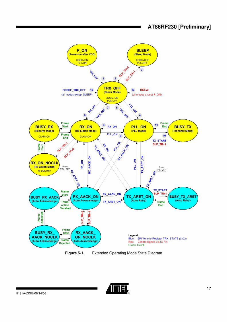
5. Extended Operating Modes
The AT86RF230 transceiver implements address filtering, automatic acknowledgement frame generation and automatic frame retransmission for peer-to-peer networks in compliance with the IEEE 802.15.4 standard. Automatic modes help to achieve low power consumption and low peak current: TX-ARET (transmit/auto-retry) and RX-AACK (receive/auto-acknowledge).
A TX-ARET transaction consists of:
• CSMA/CA
• Frame transmission (if the channel is available) and automatic CRC generation
• Reception of ACK frame (if required by frame type and ACK request)
• Retry of CSMA/CA if the channel is busy or an ACK is expected but not received
• Interrupt signaling at the end of the transaction, with exit code (success, channel busy, no ACK)
A RX-AACK frame reception consists of:
• Frame reception and automatic CRC check
• Address filtering
• Interrupt signaling that the frame was received (if it passes address filtering)
• Automatic ACK frame transmission (if the received frame passed the address filter and if an ACK is required by the frame type and ACK request)
A state diagram including these extended operating modes is shown in Figure 5-1.
5.1. Peer-to-peer Network Support The automatic modes of the AT86RF230 are designed for peer-to-peer networks and non-slotted operation, as defined in the IEEE 802.15.4 standard.
Note that automatic CRC generation can only be applied in conjunction with the TX-ARET mode, and automatic CRC check will only be applied in RX-AACK mode.
In RX-AACK mode, an ACK frame will always be sent with the data-pending bit set to zero. In TX-ARET mode, an ACK is considered to be valid if the CRC is valid, and if the sequence number of the ACK corresponds to the previously transmitted frame. The value of the “data-pending” bit is ignored.
Important Note: ACK frames will not be automatically generated for frames with either the broadcast PAN ID (0xFFFF) or a broadcast address.
17
AT86RF230 [Preliminary]
5131A-ZIGB-06/14/06
2
TRX_O
FF
SLP
_TR=1
Legend:
Blue: SPI Write to Register TRX_STATE (0x02)Red: Control signals via IC Pin
Green: Event
SLP
_TR
=0
PLL
_ON
RX_ON
PLL_ON
TRX_OFF(Clock Mode)
XOSC=ON
Pull=OFF
RX_O
N
P_ON(Power-on after VDD)
XOSC=ON
Pull=ON
SLEEP(Sleep Mode)
XOSC=OFF
Pull=OFF
(all modes except P_ON)
FORCE_TRX_OFF
(all modes except SLEEP)
Frame
Start
Frame
End
Frame
End BUSY_TX(Transmit Mode)
PLL_ON(PLL Mode)
RX_ON(Rx Listen Mode)
BUSY_RX(Receive Mode)
CLKM=ON
TX_START
SLP_TR=1
TRX_O
FF
TRX_O
FF
1
3
4
57
6
8
9
11
10
RX_ON_NOCLK(Rx Listen Mode)
CLKM=OFF
SLP_TR=1
SLP_T
R=0F
ram
e
Sta
rt
CLKM=ON
TX_ARET_ON(Auto Retry)
RX_AACK_ON(Auto Acknowledge)
BUSY_RX_AACK(Auto Acknowledge)
BUSY_TX_ARET(Auto Retry)
Frame Start
Trans-
actionFinished
RX_AACK_ON
TX_ARET_ON
TX
_A
RE
T_O
N
PL
L_O
N
TX_START
SLP_TR=1
FrameEnd
RX
_O
N
RX
_A
AC
K_O
N
PLL_O
NR
X_A
AC
K_O
NTX_A
RET_O
N
RX_AACK_
ON_NOCLK(Auto Acknowledge)
BUSY_RX_
AACK_NOCLK(Auto Acknowledge)
Frame
Start
Frame
Rejected
Fra
me
Accep
ted
RX_O
N
TX
_A
RE
T_O
NR
X_A
RE
T_O
N
From TRX_OFF
From TRX_OFF
SL
P_T
R=
1
SL
P_T
R=
0
RST=012 13
Figure 5-1. Extended Operating Mode State Diagram

18 AT86RF230 [Preliminary] 5131A-ZIGB-06/14/06
5.2. Configuration The initialization of the AT86RF230 prior to using RX-AACK or the TX-ARET mode is similar to initializing the IC prior to switching to regular RX or TX modes.
RX_AACK_ON mode is enabled after the register bits TRX_CMD in register 0x02 (TRX_STATE) is written using RX_AACK_ON. The IC is in the RX_AACK_ON mode when the register 0x01 (TRX_STATUS) changes to RX_AACK_ON or BUSY_RX_AACK. For correct RX_AACK_ON operation, the register bit TX_AUTO_CRC_ON (register 0x05) must be set to “1”.
Similarly, TX_ARET_ON mode is enabled after the register bits TRX_CMD is written with TX_ARET_ON. The IC is in the TX_ARET_ON mode after TRX_STATUS changes to TX_ARET_ON or to BUSY_TX_ARET. For correct TX-ARET operation, the register bit TX_AUTO_CRC_ON (register 0x05) must be set to “1”.
The CSMA/CA algorithm can be configured using the 0x2D (CSMA_SEED_0) and the 0x2E (CSMA_SEED_1) registers. The MIN_BE register bits sets the minimum back-off exponent (refer to the IEEE 802.15.4 standard), and the CSMA_SEED_* register bits define a random seed for the back-off-time random-number generator in the AT86RF230. The register bits MAX_CSMA_RETRIES (register 0x2C) configures how often the transceiver will retry the CSMA/CA algorithm after a busy channel is initially detected.
Both automatic modes can be exited by writing a new mode command to the register bits TRX_CMD in register 0x02 (TRX_STATE). Polling the 0x01 (TRX_STATUS) register for the new state confirms that the transceiver has left the automatic mode.
5.3. Extended Operation Mode Description
5.3.1. RX_AACK_ON
In the RX_AACK_ON mode, the transceiver listens for incoming frames.
After detecting a frame start, the transceiver will parse the frame contents for frame type and destination address. The filtering procedure described in IEEE 802.15.4 will be applied to the frame. Any frames rejected by address filtering will be discarded. A frame will also be discarded if the CRC is found to be invalid.
Otherwise, the TRX_END interrupt will be raised after the reception of the frame is completed. The controller can then upload the frame.
The transceiver also detects if an ACK frame needs to be sent. If this is true, the transceiver will automatically send an ACK frame 12 symbol periods after the end of the received frame. Only ACKs with a cleared data-pending bit will be transmitted.
No ACK will be sent if no ACK is required.
5.3.2. TX_ARET_ON
In TX_ARET_ON mode, the transceiver executes the CSMA/CA algorithm and transmits a frame downloaded by the controller. If necessary, it will check for an ACK reply, and signal the result of the transaction by raising a TRX_END interrupt. After the interrupt, the controller may read the value of the register bits TRAC_STATUS (register 0x02) to determine whether or not the transaction was successful.
The CSMA/CA transmission transaction is started by pulsing the SLP_TR pin high for at least one microsecond. The frame data must have already been downloaded. Alternatively, the controller may download the frame data while the transceiver is transmitting the preamble. In this case, it is the responsibility of the controller to ensure that the data arrives sufficiently early.
The transceiver executes the un-slotted CSMA/CA algorithm as defined by the IEEE 802.15.4 standard. If a clear channel is detected during CSMA/CA execution, the transceiver will proceed to transmit the frame. If the CSMA/CA did not detect a clear channel, the channel access will be retried as often as set by the register bits MAX_CSMA_RETRIES in register 0x2C (XAH_CTRL). In case that CSMA/CA does not detect a clear channel
19
AT86RF230 [Preliminary]
5131A-ZIGB-06/14/06
even after the maximum number of retries, it will abort the transaction, raise the TRX_END interrupt, and set the value of the TRAC_STATUS register bits to CHANNEL_ACCESS_FAILURE.
Upon the detection of a clear channel, the transceiver starts the frame transmission. It parses the frame as it is transmitted to check if an ACK reply will be expected. If no ACK is expected, the transceiver will raise an interrupt after the frame transmission completes. The value of register bits TRAC_STATUS (register 0x02) is set to SUCCESS.
On the other hand, if the transmitted frame requires an ACK, the transceiver switches into receive mode to wait for a valid ACK reply. If no valid ACK is received, the transceiver will retry the entire transaction, including CSMA/CA execution, until the frame has been acknowledged or the maximum number of retransmissions (as set by the register bits MAX_FRAME_RETRIES in register 0x2C) has been reached. In this case, the TRX_END interrupt is raised and the value of TRAC_STATUS is set to NO_ACK.
If a valid ACK is found, the TRX_END interrupt will be raised. In this case, TRAC_STATUS is set to SUCCESS.
5.3.3. RX_AACK_NOCLK
If the radio is listening for an incoming frame and the controller is not running an application, the controller can be powered down to decrease the total system power consumption. This special power down scenario (similar to RX_ON_NOCLK) for controllers running in synchronous mode is supported by the AT86RF230 using the state RX_AACK_NOCLK.
The state can only be entered by setting SLP_TR = 1 while the IC is in the RX_AACK_ON mode. The CLKM pin will be disabled 35 clock cycles after the rising edge at the SLP_TR pin. This will enable the controller to complete its power down sequence.
In RX_AACK_NOCLK mode, the transceiver listens for IEEE 802.15.4 frames. Should the AT86RF230 detect an Start-of-Frame-Delimiter, it will enter the BUSY_RX_AACK_NOCLK state, and it will start to receive the frame. If the frame passes the address filter, the AT86RF230 enters the BUSY_RX_AACK state, and the clock supplied to the micro-controller is turned back on. The controller may now process the incoming frame.
If the received frame has a valid CRC, and if it requires an acknowledgement, the transceiver will automatically generate and transmit an ACK frame.
The end of the transaction is signaled to the controller by an TRX_END interrupt. After the transaction has been completed, the transceiver will enter the RX_AACK_ON state. The transceiver will only re-enter the RX_AACK_NOCLK state when the SLP_TR has been reset to “0”, and afterwards set to “1” again.
If the transceiver is in the RX_AACK_NOCLK state, and the SLP_TR pin is reset to “0”, it will enter the RX_AACK_ON state, and it will again start to supply the micro-controller with the clock signal.

20 AT86RF230 [Preliminary] 5131A-ZIGB-06/14/06
6. Functional Description
6.1. RSSI/Energy Detection The internal limiter amplifier provides an RSSI value which reflects the current receive signal strength at the antenna pin of the AT86RF230. The RSSI is a 5-bit value indicating the receive power in steps of 3 dB (see register 0x06), and is updated every 2 µs.
The receiver ED measurement is used with the channel-scan algorithm. An ED request (write access to register 0x07) as defined by the IEEE 802.15.4 standard has a measurement time of 128 µs. The ED measurement result is accessible after the measurement time at register 0x07 (PHY_ED_LEVEL). With every frame reception (SFD detection), an ED measurement is automatically started. The ED measurement result has the same range as the RSSI value (register 0x06), but with a 1 dB resolution.
6.2. Link Quality Indication The IEEE 802.15.4 standard defines the link quality indication (LQI) measurement as a “characterization of the strength and/or quality of a received packet”. The LQI measurement of the AT86RF230 is implemented as a characterization of both the quality and signal strength. An average correlation value of multiple symbols is calculated and appended to each frame after scaling to a value ranging from 0 to 255. The minimum LQI value of 0 is associated with a low signal quality, resulting from high signal distortions, and/or a signal strength that is below the receiver sensitivity. The maximum value of 255 is associated with a signal strength higher than the receiver sensitivity and a high signal quality resulting from low signal distortions. Signal distortions are mainly generated by interference and multipath propagation.
6.3. Clear Channel Assessment The IEEE 802.15.4 standard defines three clear channel assessment (CCA) modes:
• Mode 1: energy above threshold only
• Mode 2: carrier sense only
• Mode 3: carrier sense with energy above threshold All three modes are available in AT86RF230. The modes are configurable via register 0x08 (PHY_CC_CCA). A CCA request is initiated by writing to bit 7 in register 0x08 (PHY_CC_CCA). After the CCA evaluation time of 128 µs, the CCA result is accessible at register 0x01 (TRX_STATUS) bits 6 and 7. Bit 7 indicates whether the CCA measurement is finished or not, bit 6 indicates a busy (bit 6 = 0) or clear channel. (bit 6 = 1)
The CCA modes are further configurable using register 0x09 (CCA_THRES).
The 4-bit value CCA_CS_THRES can be used for fine tuning the sensitivity of the CCA carrier sense algorithm. Higher values increase the probability of clear channel detection.
The other 4-bit value (CCA_ED_THRES) of register 0x09 (CCA_THRES) defines the received power threshold of the “energy above threshold” algorithm. Any received power above this level will indicate a busy channel. The threshold is calculated by -91+2·CCA_ED_THRES [dBm], resulting in a range of -91 dBm to -61 dBm.
6.4. Voltage Regulators Two identical low-dropout voltage regulators are integrated within the AT86RF230. The AVREG provides the regulated 1.8V supply voltage for the analog section and the DVREG supplies the low-voltage digital section. A simplified schematic is shown in Figure 6-1. The voltage regulators are connected internally to the external unregulated supply voltage VDD. The regulated output voltage is available on pin VDEC1 or VDEC2. External decoupling capacitors should be connected to these pins to stabilize the regulated supply voltage. A decoupling
capacitor value of 1 µF is recommended for stable operation of the voltage regulators (see chapter 9), but it can

21
AT86RF230 [Preliminary]
5131A-ZIGB-06/14/06
range from 400 nF to 10 µF. A higher capacitor value provides better voltage stability, but increases the voltage regulator settling time.
Bandgapvoltage
reference
1.25V
VDEC
VDD
VREG_TRIM[1:0]
Figure 6-1. Simplified Schematic of VREG
The voltage regulators can be configured using the register 0x10 (VREG_CTRL). The read-only bit values AVDD_OK = 1 and DVDD_OK = 1 indicate a stable, regulated supply voltage.
It is possible to use external voltage regulators instead of the internal regulators. For this special application the internal regulators need to be switched off by setting the register bits to the values AVREG_EXT = 1 and DVREG_EXT = 1. A regulated external supply voltage of 1.8V needs to be connected to the pins VDEC1 and VDEC2. When turning on the external supply, ensure a sufficiently long stabilization time before interacting with the AT86RF230.
6.5. Battery Monitor The battery monitor (BATMON) detects and signals a low battery or supply voltage. This is done by comparing the current voltage on the VDD pins with a programmable internal threshold voltage. Figure 6-2 shows the simplified schematic of the BATMON with the most important input and output signals.
BATMON_HR
BATMON_VTH
4
VDD
Threshold Voltage
BATMON_OK
„1“
BATMON_IRQ
For input-to-output mappingsee control register
0x11 (BATMON)
DAC
+
-
D
Q
clear
Figure 6-2. Simplified Schematic of BATMON

22 AT86RF230 [Preliminary] 5131A-ZIGB-06/14/06
The BATMON can be configured using the register 0x11 (BATMON). BATMON_VTH[3:0] sets the threshold voltage. It is programmable with a resolution of 75 mV in the upper voltage range (BATMON_HR = 1) and with a resolution of 50 mV in the lower voltage range (BATMON_HR = 0). The signal-bit BATMON_OK indicates the current value of the battery voltage:
• If BATMON_OK is ”0”, the battery voltage is lower than the threshold voltage
• If BATMON_OK is “1”, the battery voltage is higher than the threshold voltage Furthermore, an interrupt (IRQ7) is automatically generated when the battery voltage falls below the programmed threshold (see control register 0x0F and 0x0E). The interrupt appears only when BATMON_OK changes from “1” to ”0”. No interrupt will be generated when:
• the battery voltage is under the default 1.8V threshold at power up (BATMON_OK was never ”1”), or
• a new threshold is set, which is above the current battery voltage (BATMON_OK remains ”0”). After setting a new threshold, the value BATMON_OK should be read out to verify the current supply voltage value.
When the battery voltage is close to the programmed threshold voltage, noise or temporary voltage drops can generate a lot of unwanted interrupts initiated by a toggling BATMON_OK signal. To avoid this:
• disable the IRQ7-bit in IRQ mask register after the first interrupt and treat the battery as empty, or
• set a lower threshold value after the first interrupt. Note that the battery monitor is inactive during PON and SLEEP modes, see control register 0x01 (TRX_STATUS).
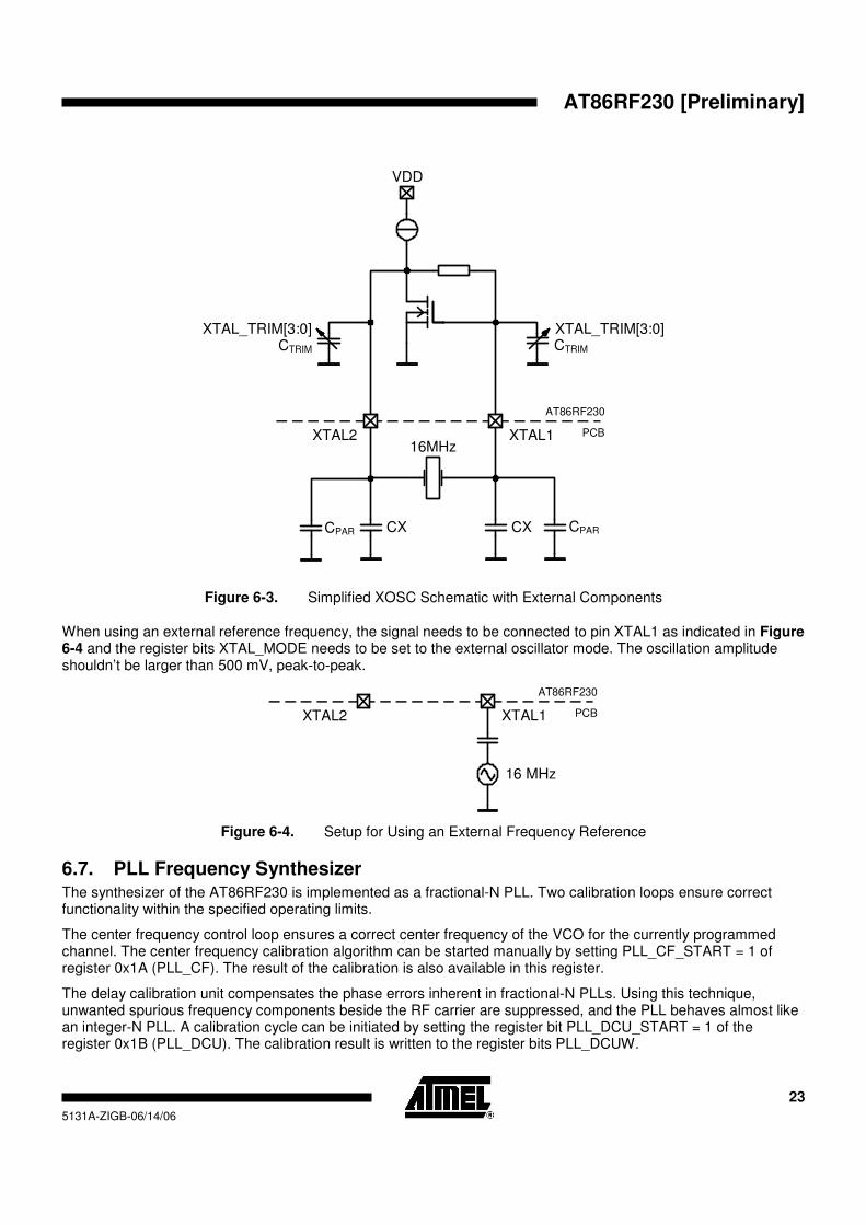
6.6. Crystal Oscillator The crystal oscillator generates the reference frequency for the AT86RF230. All other internally-generated frequencies in the transceiver are derived from this unique frequency. Therefore the overall system performance is mainly based on the accuracy of this reference frequency. The external components of the crystal oscillator should be selected carefully and the related board layout should be done meticulously.
The register 0x12 (XOSC_CTRL) provides access to the control signals of the oscillator. Basically, two operating modes are supported. A reference frequency can be fed to the internal circuitry by using an external clock reference or by setting up the integrated oscillator as described in Figure 6-3.
Using the internal oscillator, the oscillation frequency strongly depends on the load capacitance seen by the crystal between the crystal pins XTAL1 and XTAL2. The total load capacitance must be equal to the specified load capacitance CL of the crystal itself. It consists of the external capacitors CX and parasitic capacitances connected to the XTAL nodes. In Figure 6-3, all parasitic capacitances, such as PCB stray capacitances and the pin input capacitance, are summarized to CPAR. Additional internal trimming capacitors CTRIM are available. Any value in the range from 0 pF to 4.8 pF with a 0.3 pF resolution is selectable using the register bits XTAL_TRIM[3:0]. To calculate the total load capacitance, the following formula can be used CL = 0.5*(CX+CTRIM+CPAR).
The trimming capacitors provide the possibility of an easy adjustment of frequency changes caused by production process variations or by tolerances of the external components. Note that the oscillation frequency can be reduced only by increasing the trimming capacitance. The frequency deviation caused by one unit of CTRIM decreases with increasing crystal load capacitor values.
An amplitude control circuit is included to ensure stable operation with different operating conditions and different crystal types. A high current during the amplitude build-up phase guarantees a low start-up time. At stable operation, the current is reduced to the amount necessary for a robust operation. This also keeps the drive level of the crystal low.
Generally, crystals with a higher load capacitance are less sensitive to parasitic pulling effects caused by external component variations or by variations of board and circuit parasitics. On the other hand, a larger crystal load capacitance results in a longer start-up time and a higher steady state current consumption.
23
AT86RF230 [Preliminary]
5131A-ZIGB-06/14/06
CX CX
16MHzXTAL1XTAL2
VDD
CTRIMCTRIM
CPARCPAR
AT86RF230
PCB
XTAL_TRIM[3:0]XTAL_TRIM[3:0]
Figure 6-3. Simplified XOSC Schematic with External Components
When using an external reference frequency, the signal needs to be connected to pin XTAL1 as indicated in Figure 6-4 and the register bits XTAL_MODE needs to be set to the external oscillator mode. The oscillation amplitude shouldn’t be larger than 500 mV, peak-to-peak.
XTAL1XTAL2
AT86RF230
PCB
16 MHz
Figure 6-4. Setup for Using an External Frequency Reference
6.7. PLL Frequency Synthesizer The synthesizer of the AT86RF230 is implemented as a fractional-N PLL. Two calibration loops ensure correct functionality within the specified operating limits.
The center frequency control loop ensures a correct center frequency of the VCO for the currently programmed channel. The center frequency calibration algorithm can be started manually by setting PLL_CF_START = 1 of register 0x1A (PLL_CF). The result of the calibration is also available in this register.
The delay calibration unit compensates the phase errors inherent in fractional-N PLLs. Using this technique, unwanted spurious frequency components beside the RF carrier are suppressed, and the PLL behaves almost like an integer-N PLL. A calibration cycle can be initiated by setting the register bit PLL_DCU_START = 1 of the register 0x1B (PLL_DCU). The calibration result is written to the register bits PLL_DCUW.

24 AT86RF230 [Preliminary] 5131A-ZIGB-06/14/06
Both calibration routines will be initiated automatically when the PLL is turned on. Additionally, the center frequency calibration is running when the PLL is programmed to a different channel (register 0x08 bits [4:0]). If the PLL is not turned off for a long time, the control loops should be manually initiated from time to time. The calibration interval depends on environment temperature variations but should not be longer than 5 min.
6.8. Automatic Filter Tuning The filter-tuning unit is a separate building block within the AT86RF230. A calibration cycle is initiated automatically when entering the TRX_OFF state from either the SLEEP, RESET or P_ON states. The result of the calibration is the 6-bit word FTNV, and is written to the register 0x18 (FTN_CTRL).
The filter-tuning value FTNV is used to provide a stable SSBF transfer function and PLL loop-filter time constant independent of temperature effects and part-to-part variations.
It is possible to trigger the calibration algorithm manually by setting the register bit FTN_START = 1.

25
AT86RF230 [Preliminary]
5131A-ZIGB-06/14/06
7. PHY to Micro-Controller Interface
In the following paragraphs, the PHY to micro-controller interface is defined. The SPI protocol and timing access are shown, as well as buffer access modes with examples.
Controllers with an SPI interface such as an AVR will work with the AT86RF230 interface. The SPI interface is used for both register programming as well as for frame transfer. The additional control signals are connected to the GPIO interface of the controller. Figure 7-1 shows the signals which need to be connected between the controller and the transceiver. The CLKM signal can be used as a controller main clock (synchronous mode) or as software timer reference (asynchronous mode).
Micro-Controller AT86RF230
MOSI
MISO
SCLK
CLKM
IRQ
SLP_TR
MOSI
MISO
SCLK
GPIO1/CLK
GPIO2/IRQ
GPIO3
MOSI
MISO
SCLK
CLKM
IRQ
SLP_TR
GPIO4S
PI
SEL SELSEL
RSTRST
Figure 7-1. PHY-HOST Interface
7.1. SPI Protocol SPI is used to program control registers as well as to transfer data frames between the controller and the
AT86RF230. The additional signals CLKM, IRQ, SLP_TR and RST are connected to the GPIO interface of the
controller.
The internal 128-byte frame buffer can keep one TX or one RX frame of maximum length at a time. This offers a very flexible data rate over the SPI interface.
SEL
SCLK
MISO
MOSI
SLP_TR
Bit7 Bit6 Bit5 Bit4 Bit3 Bit2 Bit1 Bit0 Bit7 Bit6 Bit5 Bit4 Bit3 Bit2 Bit1 Bit0
Bit7 Bit6 Bit5 Bit4 Bit3 Bit2 Bit1 Bit0 Bit7 Bit6 Bit5 Bit4 Bit3 Bit2 Bit1 Bit0
t7
t4
t2t1 t5 t6
t3
Figure 7-2. SPI Timing

26 AT86RF230 [Preliminary] 5131A-ZIGB-06/14/06
The interface is designed to work in synchronous or asynchronous mode. In synchronous mode, the CLKM output of the transceiver IC is used as the master clock of the controller. The SPI clock can be any integer-divided clock ratio up to 8 MHz.
Nevertheless, usage of an independent controller clock for an asynchronous interface is possible. In asynchronous mode, the maximum SPI clock speed is limited to 7.5 MHz. The external CLKM output signal is not required and can be disabled.
SEL enables the MISO output driver of the AT86RF230. If the driver is disabled, there is no internal pull-up
resistor connected to it. Driving the appropriate signal level must be ensured by the master device or an external pull-up resistor.
The SPI is a byte-oriented serial interface. All bytes are transferred MSB first. Every SPI transfer starts with
0SEL = and this signal is asserted low as long as one consecutive SPI access occurs. One consecutive access
includes two or more bytes depending on the access mode described later. If 0SEL = goes high before the end of
one complete access, the internal bit counter is reset and the transferred data are lost.
Both sides of the interface (master and slave) contain an 8-bit shift register. The master starts the transfer by
asserting 0SEL = . After the 8-bit shift register is loaded, the master generates eight SPI clocks in order to transfer
the data to the slave, and at the same time the slave transmits one byte to the master shift register. If the master wants to receive one byte of data it must also transmit one byte to the slave. Every transfer starts with a command byte. This command byte contains the access mode information as well as additional mode-dependent bits. During command byte transfer, the AT86RF230 returns a byte containing “0”.
Bit 7 Bit 6 (R/W)
Bit 5 Bit 4 Bit 3 Bit 2 Bit 1 Bit 0 Mode
1 0 Register address [5:0] Short mode (register read access)
1 1 Register address [5:0] Short mode (register write access)
0 0 1 Reserved Frame receive mode
0 1 1 Reserved Frame transmit mode
0 0 0 Reserved SRAM read access mode
0 1 0 Reserved SRAM write access mode
Table 7-1. Interface Access Mode Overview
7.2. Register Access Mode (Short Mode) The register access mode is a two-byte read/write operation. The first byte contains the control information (mode identifier bit 7, read/write select bit 6, and a 6-bit address). The second byte contains the read or write data. In this mode a maximum of 64 consecutive registers can be addressed.
byte 2byte 1
address[5:0] data[7:0]R/W
1=write
0=read
1
Figure 7-3. Register Short Mode Access

27
AT86RF230 [Preliminary]
5131A-ZIGB-06/14/06
CLKM
SEL
SCLK
MOSI
MISO
COMMAND WRITE DATA COMMAND XX
XX XX XX READ DATA
Write Register Access Read Register Access
Figure 7-4. SPI Register Access Sequence
7.3. Frame Buffer Access Modes (Long Modes) These modes are used to upload or download frames as well as access the frame buffer directly. Each transfer starts with a control byte. If this byte indicates a frame upload or download, the next byte indicates the frame length followed by the PSDU data. In receive mode, after the PSDU data has been received, one more byte is attached, containing LQI information.
The number of bytes for one frame access must be calculated by the controller as follows:
Transmit: byte_count = command byte + frame length byte + frame length Receive: byte_count = command byte + frame length byte + frame length + LQI byte That means there is a maximum frame buffer access of 129 bytes for TX and 130 bytes for RX.
byte 3 byte nbyte n-1byte 2byte 1
control[4:0](reserved)
frame_length[7:0]TX/RX
00 data[7:0] data[7:0]1 LQI[7:0]
Figure 7-5. Frame Receive Mode
byte 3 byte nbyte 2byte 1
control[4:0](reserved)
frame_length[7:0]TX/RX
10 data[7:0] data[7:0]1
Figure 7-6. Frame Transmit Mode
If the control byte indicates SRAM access mode, the next byte contains the start address. As long as SEL is low,
every subsequent byte read or write increments the address counter of the frame buffer.
byte 1 byte 2 byte 3 byte n
control[4:0](reserved)
address[7:0]R/W
1=write
0=read
0 data[7:0] data[7:0]0
Figure 7-7. SRAM Access Mode

28 AT86RF230 [Preliminary] 5131A-ZIGB-06/14/06
7.4. Frame Receive Procedure The following transactions are required to receive a frame over the SPI:
IRQ issued
read IRQ status register (register access)
IRQ line deasserted
receiving frame data (frame receive mode)
PH
Y
Co
ntr
olle
r
Figure 7-8. Receive Frame Transactions Between AT86RF230 and Controller
CLKM
SEL
SCLK
MOSI
MISO
IRQ
SLP_TR
COMMAND XX COMMAND XX XX XX XX XX XX
XX READ DATA XX FRAME LENGTH FRAME DATA 1 FRAME DATA 2 FRAME DATA 3 FRAME DATA n LQI Value
IRQ issued
IRQ_status_read Frame_upload
Figure 7-9. Frame Receive Sequence
7.5. Frame Transmit Procedure The following transactions are required to transmit a frame over SPI:
write frame data to transceiver (frame transmit mode)
write tx_start bit to register (register access) or assert SLP_TR (depends on configuration)
PH
Y
Contr
olle
r
Figure 7-10. Transmit Frame Transactions Between AT86RF230 and Controller
29
AT86RF230 [Preliminary]
5131A-ZIGB-06/14/06
CLKM
SEL
SCLK
MOSI
MISO
IRQ
SLP_TR
COMMAND FRAME LENGTH FRAME DATA 1 FRAME DATA 2 FRAME DATA 3 FRAME DATA n
XX XX XX XX XX XX
Frame_download
Transmit Start
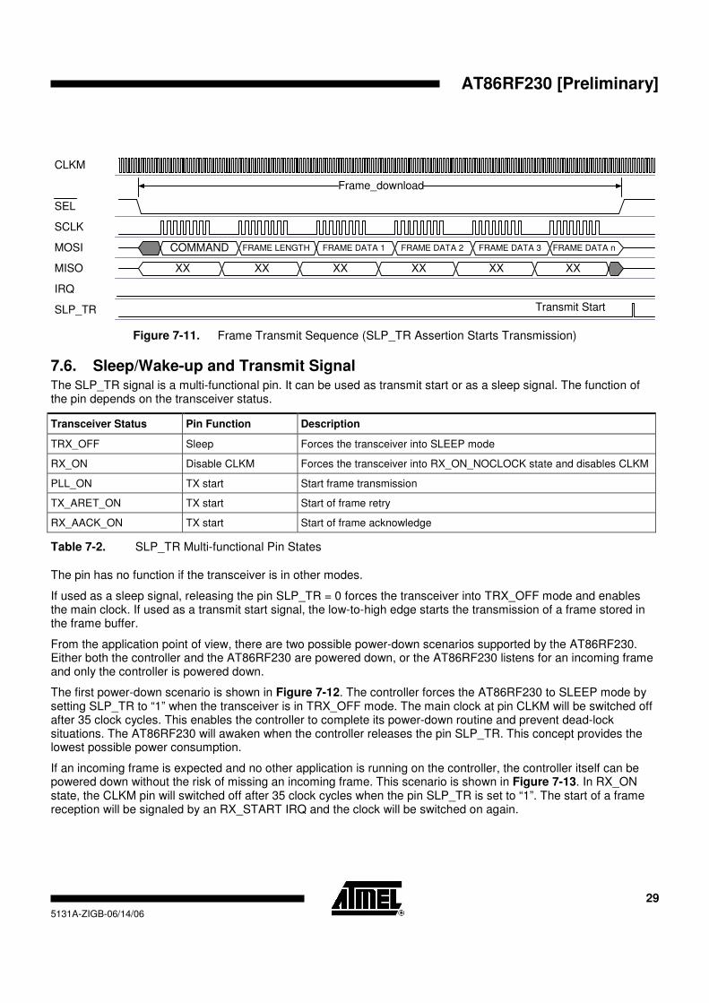
Figure 7-11. Frame Transmit Sequence (SLP_TR Assertion Starts Transmission)
7.6. Sleep/Wake-up and Transmit Signal The SLP_TR signal is a multi-functional pin. It can be used as transmit start or as a sleep signal. The function of the pin depends on the transceiver status.
Transceiver Status Pin Function Description
TRX_OFF Sleep Forces the transceiver into SLEEP mode
RX_ON Disable CLKM Forces the transceiver into RX_ON_NOCLOCK state and disables CLKM
PLL_ON TX start Start frame transmission
TX_ARET_ON TX start Start of frame retry
RX_AACK_ON TX start Start of frame acknowledge
Table 7-2. SLP_TR Multi-functional Pin States
The pin has no function if the transceiver is in other modes.
If used as a sleep signal, releasing the pin SLP_TR = 0 forces the transceiver into TRX_OFF mode and enables the main clock. If used as a transmit start signal, the low-to-high edge starts the transmission of a frame stored in the frame buffer.
From the application point of view, there are two possible power-down scenarios supported by the AT86RF230. Either both the controller and the AT86RF230 are powered down, or the AT86RF230 listens for an incoming frame and only the controller is powered down.
The first power-down scenario is shown in Figure 7-12. The controller forces the AT86RF230 to SLEEP mode by setting SLP_TR to “1” when the transceiver is in TRX_OFF mode. The main clock at pin CLKM will be switched off after 35 clock cycles. This enables the controller to complete its power-down routine and prevent dead-lock situations. The AT86RF230 will awaken when the controller releases the pin SLP_TR. This concept provides the lowest possible power consumption.
If an incoming frame is expected and no other application is running on the controller, the controller itself can be powered down without the risk of missing an incoming frame. This scenario is shown in Figure 7-13. In RX_ON state, the CLKM pin will switched off after 35 clock cycles when the pin SLP_TR is set to “1”. The start of a frame reception will be signaled by an RX_START IRQ and the clock will be switched on again.

30 AT86RF230 [Preliminary] 5131A-ZIGB-06/14/06
CLKM
SLP_TR
async timer (controller) elapsed
35 main clock cycles
Figure 7-12. Sleep and Wake-up Initiated by Asynchronous Controller Timer Output
CLKM
SLP_TR
IRQ
transceiver IRQ issued
35 main clock cycles
Figure 7-13. Wake-up Initiated by Transceiver Interrupt
7.7. Interrupt Logic The AT86RF230 can differentiate between six interrupt events. Each interrupt can be enabled or disabled by writing the corresponding bit to the interrupt mask register. All six internal interrupt lines are combined via logical “OR” to one external interrupt line. Internally, each interrupt is stored in a separate bit of the interrupt status register. If the external interrupt line is set, the controller must first read the interrupt status register to determine the source of the interrupt. A read access to this register clears the interrupt status register and also the external interrupt line. The interrupt will not be cleared automatically when the event that caused the IRQ is not valid anymore. Exception: the PLL_LOCK IRQ will clear the PLL_UNLOCK IRQ and vice versa.
For a detailed description of the interrupt status register, please refer to register 0x0F (IRQ_STATUS).
Note: After a reset signal, all interrupts are enabled. Special settings in the register 0x0E (IRQ_MASK) need to be renewed.

31
AT86RF230 [Preliminary]
5131A-ZIGB-06/14/06
8. Control Registers
The AT86RF230 provides a register space of 64 8-bit registers, which is used to configure the IC as well as to store signaling information read by the firmware.
Note that all registers not mentioned within the following table are reserved for internal use and must not be written to. When writing to a non-reserved register, any individual bits of that register marked as reserved can only be overwritten by their reset value.
Reg.-Addr. Register Name Description
0x01 TRX_STATUS Transceiver status, CCA result
0x02 TRX_STATE State/mode control
0x03 TRX_CTRL_0 Driver current and controller clock setting
0x05 PHY_TX_PWR TX power setting
0x06 PHY_RSSI RSSI value
0x07 PHY_ED_LEVEL RX energy level
0x08 PHY_CC_CCA CCA mode configuration, CCA request, channel setting
0x09 CCA_THRES CCA_ED and CCA_CS threshold
0x0E IRQ_MASK Interrupt mask
0x0F IRQ_STATUS Interrupt status
0x10 VREG_CTRL Voltage regulator control
0x11 BATMON Battery monitor control
0x12 XOSC_CTRL Crystal oscillator control
0x18 FTN_CTRL Filter tuning control
0x1A PLL_CF PLL center frequency calibration
0x1B PLL_DCU PLL delay calibration
0x1C PART_NUM Part ID
0x1D VERSION_NUM Version ID
0x1E MAN_ID_0 Manufacturer ID, lower 8 bits
0x1F MAN_ID_1 Manufacturer ID, higher 8 bits
0x20 SHORT_ADDR_0 Short address for address recognition
0x21 SHORT_ADDR_1 Short address for address recognition
0x22 PAN_ID_0 PAN address for address recognition
0x23 PAN_ID_1 PAN address for address recognition
0x24 IEEE_ADDR_0 Current node IEEE address for address recognition
0x25 IEEE_ADDR_1 Current node IEEE address for address recognition
0x26 IEEE_ADDR_2 Current node IEEE address for address recognition
0x27 IEEE_ADDR_3 Current node IEEE address for address recognition
0x28 IEEE_ADDR_4 Current node IEEE address for address recognition

32 AT86RF230 [Preliminary] 5131A-ZIGB-06/14/06
Reg.-Addr. Register Name Description
0x29 IEEE_ADDR_5 Current node IEEE address for address recognition
0x2A IEEE_ADDR_6 Current node IEEE address for address recognition
0x2B IEEE_ADDR_7 Current node IEEE address for address recognition
0x2C XAH_CTRL Retries value control
0x2D CSMA_SEED_0 CSMA seed value
0x2E CSMA_SEED_1 CSMA seed value
Table 8-1. Configuration registers overview
Bit Field Name Reset R/W Comments
7 CCA_DONE 0 R 1’d0: CCA calculation in progress 1’d1: CCA calculation done
6 CCA_STATUS 0 R Indicates an idle channel from CCA module. CHANNEL_IDLE: 1’d0: channel is busy 1’d1: channel is idle
5 0 R Reserved
4:0 TRX_STATUS 0 R Signals the current transceiver status. TRANSCEIVER_STATUS: 5’d0: P_ON 5’d1: BUSY_RX 5’d2: BUSY_TX 5’d6: RX_ON 5’d8: TRX_OFF (CLK Mode) 5’d9: PLL_ON (TX_ON) 5’d15: SLEEP 5’d17: BUSY_RX_AACK 5’d18: BUSY_TX_ARET 5’d22: RX_AACK_ON 5’d25: TX_ARET_ON 5’d28: RX_ON_NOCLK 5’d29: RX_AACK_ON_NOCLK 5’d30: BUSY_RX_AACK_NOCLK 5’d31: state transition
Table 8-2. 0x01 - TRX_STATUS
Note: A register read will reset the CCA_STATUS bit and the CCA_DONE bit if a CCA calculation was done (CCA_DONE = 1).

33
AT86RF230 [Preliminary]
5131A-ZIGB-06/14/06
Bit Field Name Reset R/W Comments
7:5 TRAC_STATUS 0 R 3’d0: SUCCESS 3’d3: CHANNEL_ACCESS_FAILURE 3’d5: NO_ACK All other values are reserved.
4:0 TRX_CMD 0 R/W Transceiver control commands: 5’d0: NOP 5’d2: TX_START 5’d3: FORCE_TRX_OFF 5’d6: RX_ON 5’d8: TRX_OFF (CLK Mode) 5’d9: PLL_ON (TX_ON) 5’d22: RX_AACK_ON 5’d25: TX_ARET_ON All other values are mapped to NOP.
Table 8-3. 0x02 - TRX_STATE
Note: TRX_CMD = “0” after power on reset (POR).
Frame transmission starts 16 µs after TX_START command.
Bit Field Name Reset R/W Comments
7:6 PAD_IO 0 R/W Set the output driver current of digital pads (except CLKM pad). 2’d0: 2 mA 2’d1: 4 mA 2’d2: 6 mA 2’d3: 8 mA
5:4 PAD_IO_CLKM 1 R/W Set the output driver current of CLKM. 2’d0: 2 mA 2’d1: 4 mA 2’d2: 6 mA 2’d3: 8 mA
3 CLKM_SHA_SEL 1 R/W Shadow the CLKM_CTRL clock changes. If the mode is enabled, changes to the CLKM_CTRL bits take effect only when the IC leaves the SLEEP mode. 1’d0: disable (on the fly) 1’d1: enable (shadow)
2:0 CLKM_CTRL 1 R/W Controls the clock frequency at the CLKM pad. 3’d0: no clock 3’d1: 1 MHz 3’d2: 2 MHz 3’d3: 4 MHz 3’d4: 8 MHz 3’d5: 16 MHz 3’d6: no clock 3’d7: no clock
Table 8-4. 0x03 - TRX_CTRL_0

34 AT86RF230 [Preliminary] 5131A-ZIGB-06/14/06
Bit Field Name Reset R/W Comments
7 TX_AUTO_CRC_ON 0 R/W AUTO_CRC mode: 1’d0: disable 1’d1: enable
6:4 0 R Reserved
TX Power Mapping
TX Power Setting Output Power [dBm]
0 3.0
1 2.6
2 2.1
3 1.6
4 1.1
5 0.5
6 -0.2
7 -1.2
8 -2.2
9 -3.2
10 -4.2
11 -5.2
12 -7.2
13 -9.2
14 -12.2
3:0 TX_PWR 0 R/W
15 -17.2
Table 8-5. 0x05 - PHY_TX_PWR
Bit Field Name Reset R/W Comments
7:5 0 R Reserved
4:0 RSSI 0 R 5’d0: RX input level < -91 dBm 5’d27: RX input level > -10 dBm RSSI is a linear curve on a logarithmic input power scale (dBm) with a 3 dB step width.
Table 8-6. 0x06 - PHY_RSSI

35
AT86RF230 [Preliminary]
5131A-ZIGB-06/14/06
Bit Field Name Reset R/W Comments
7:0 ED_LEVEL 0 R ED level for current channel. The min. ED value (0) indicates receiver power less than or equal to -91 dBm. The range is 84 dB with a resolution of 1 dB and an absolute accuracy of ±5 dB.
Table 8-7. 0x07 - PHY_ED_LEVEL
Note: A write access initiates the ED measurement (ED.request).
Bit Field Name Reset R/W Comments
7 CCA_REQUEST 0 R/W 1’d1: starts a CCA check (CCA.request) read value always returns with “0”
6:5 CCA_MODE 1 R/W CCA Mode: 2’d0: Mode 1, energy above threshold 2’d1: Mode 1, energy above threshold 2’d2: Mode 2, carrier sense only 2’d3: Mode 3, carrier sense with energy above threshold
Channel: According to IEEE802.15.4 only 11 to 26 are valid. All unused values are reserved.
Channel Mapping
Channel Number Frequency [MHz]
11 2405
12 2410
13 2415
14 2420
15 2425
16 2430
17 2435
18 2440
19 2445
20 2450
21 2455
22 2460
23 2465
24 2470
25 2475
4:0 CHANNEL 11 R/W
26 2480
Table 8-8. 0x08 - PHY_CC_CCA

36 AT86RF230 [Preliminary] 5131A-ZIGB-06/14/06
Bit Field Name Reset R/W Comments
7:4 CCA_CS_THRES 12 R/W Threshold for CCA_CS
3:0 CCA_ED_THRES 7 R/W An ED value above the threshold signals a busy channel during a CCA_ED measurement.
Table 8-9. 0x09 - CCA_THRES
Note: CCA_ED_THRES: The CCA_ED request will indicate a busy channel, if the measured receive power is above -91 dBm + 2*CCA_ED_THRES[dB].
Bit Field Name Reset R/W Comments
7:0 IRQ_MASK 255 R/W Mask register for IRQs. If bit is set to high, then the IRQ is enabled. If bit is set to low, then the IRQ is disabled. IRQ_MASK[7] corresponds to IRQ_7. IRQ_MASK[0] corresponds to IRQ_0.
Table 8-10. 0x0E - IRQ_MASK
Note: The occurrence of an interrupt will be signaled over the IRQ wire.
Bit Field Name Reset R/W Comments
7 IRQ_7 0 R BAT_LOW: signals low battery
6 IRQ_6 0 R TRX_UR: signals a FIFO underrun
5 IRQ_5 0 R Reserved
4 IRQ_4 0 R Reserved
3 IRQ_3 0 R TRX_END: signals end of frame (transmit and receive)
2 IRQ_2 0 R RX_START: signals beginning of receive frame
1 IRQ_1 0 R PLL_UNLOCK: PLL goes from lock to unlock state
0 IRQ_0 0 R PLL_LOCK: PLL goes from unlock to lock state
Table 8-11. 0x0F - IRQ_STATUS
Note: The occurrence of an interrupt will be signaled over the IRQ wire. A read access will reset the interrupt bits.
Bit Field Name Reset R/W Comments
7 AVREG_EXT 0 R/W 1’d0: use internal analog voltage regulator 1’d1: use external voltage regulator
6 AVDD_OK 0 R 1’d0: analog voltage regulator is disabled 1’d1: internal analog voltage is correct and stable
5:4 AVREG_TRIM 0 R/W Controls the voltage of the analog voltage regulator. 2’d0: 1.80V 2’d1: 1.75V 2’d2: 1.84V 2’d3: 1.88V

37
AT86RF230 [Preliminary]
5131A-ZIGB-06/14/06
Bit Field Name Reset R/W Comments
3 DVREG_EXT 0 R/W 1’d0: use internal digital voltage regulator 1’d1: use external voltage regulator
2 DVDD_OK 0 R 1’d0: digital voltage regulator is disabled 1’d1: internal digital voltage is correct and stable
1:0 DVREG_TRIM 0 R/W Controls the voltage of the digital voltage regulator. 2’d0: 1.80V 2’d1: 1.75V 2’d2: 1.84V 2’d3: 1.88V
Table 8-12. 0x10 - VREG_CTRL
Bit Field Name Reset R/W Comments
7:6 0 R Reserved
5 BATMON_OK 0 R Result of battery monitor: 1’d0: not valid (VDD < BATMON_VTH) 1’d1: valid (VDD > BATMON_VTH)
4 BATMON_HR 0 R/W High range switch (mapping see BATMON_VTH)
Threshold voltage:
BATMON_VTH Mapping
Value Voltage [V] BATMON_HR = ”1”
Voltage [V] BATMON_HR = ”0”
0 2.550 1.70
1 2.625 1.75
2 2.700 1.80
3 2.775 1.85
4 2.850 1.90
5 2.925 1.95
6 3.000 2.00
7 3.075 2.05
8 3.150 2.10
9 3.225 2.15
10 3.300 2.20
11 3.375 2.25
12 3.450 2.30
13 3.525 2.35
14 3.600 2.40
3:0 BATMON_VTH 2 R/W
15 3.675 2.45
Table 8-13. 0x11 - BATMON
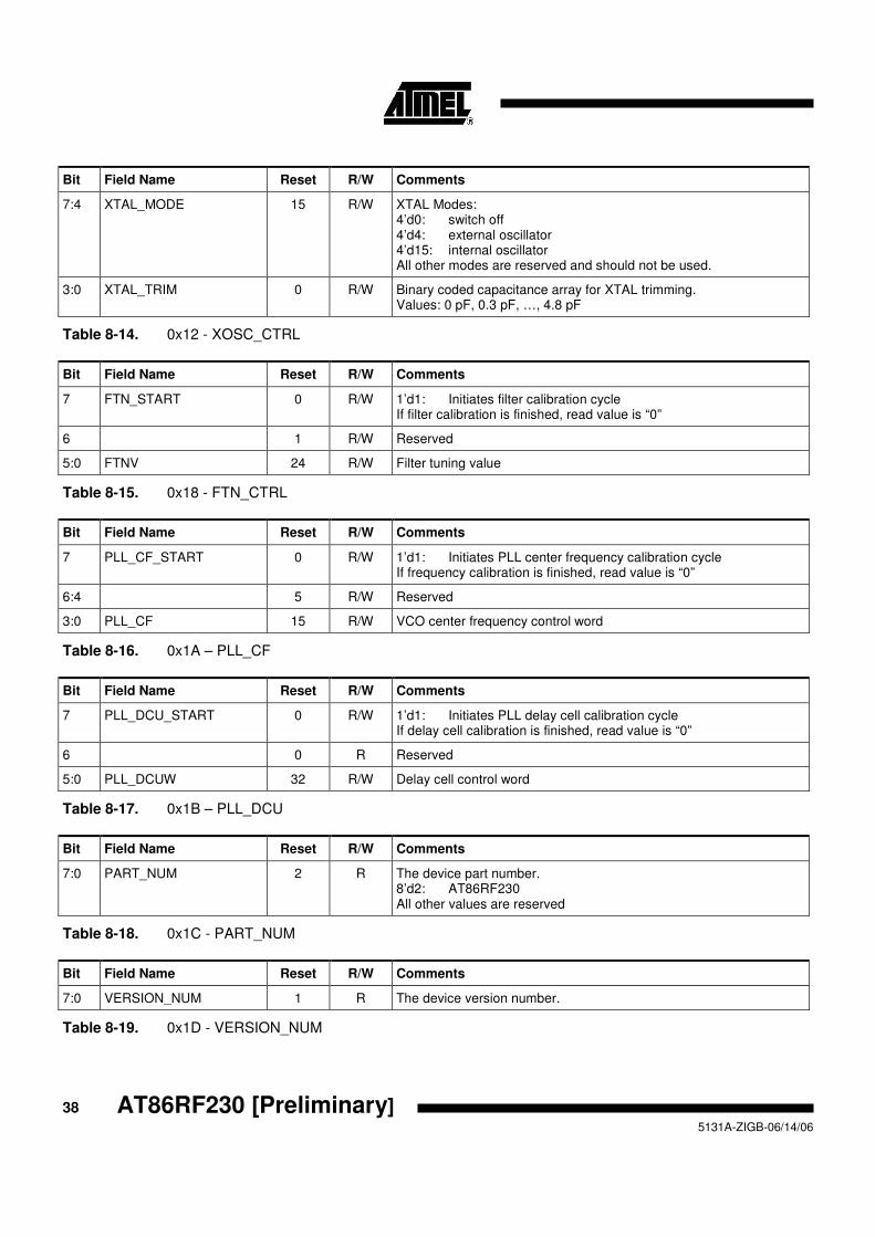
38 AT86RF230 [Preliminary] 5131A-ZIGB-06/14/06
Bit Field Name Reset R/W Comments
7:4 XTAL_MODE 15 R/W XTAL Modes: 4’d0: switch off 4’d4: external oscillator 4’d15: internal oscillator All other modes are reserved and should not be used.
3:0 XTAL_TRIM 0 R/W Binary coded capacitance array for XTAL trimming. Values: 0 pF, 0.3 pF, …, 4.8 pF
Table 8-14. 0x12 - XOSC_CTRL
Bit Field Name Reset R/W Comments
7 FTN_START 0 R/W 1’d1: Initiates filter calibration cycle If filter calibration is finished, read value is “0”
6 1 R/W Reserved
5:0 FTNV 24 R/W Filter tuning value
Table 8-15. 0x18 - FTN_CTRL
Bit Field Name Reset R/W Comments
7 PLL_CF_START 0 R/W 1’d1: Initiates PLL center frequency calibration cycle If frequency calibration is finished, read value is “0”
6:4 5 R/W Reserved
3:0 PLL_CF 15 R/W VCO center frequency control word
Table 8-16. 0x1A – PLL_CF
Bit Field Name Reset R/W Comments
7 PLL_DCU_START 0 R/W 1’d1: Initiates PLL delay cell calibration cycle If delay cell calibration is finished, read value is “0”
6 0 R Reserved
5:0 PLL_DCUW 32 R/W Delay cell control word
Table 8-17. 0x1B – PLL_DCU
Bit Field Name Reset R/W Comments
7:0 PART_NUM 2 R The device part number. 8’d2: AT86RF230 All other values are reserved
Table 8-18. 0x1C - PART_NUM
Bit Field Name Reset R/W Comments
7:0 VERSION_NUM 1 R The device version number.
Table 8-19. 0x1D - VERSION_NUM

39
AT86RF230 [Preliminary]
5131A-ZIGB-06/14/06
Bit Field Name Reset R/W Comments
7:0 MAN_ID_0 31 R JEDEC manufacturer ID is 32’h 00_00_00_1F for Atmel, bits[7:0]
Table 8-20. 0x1E - MAN_ID_0
Bit Field Name Reset R/W Comments
7:0 MAN_ID_1 0 R JEDEC manufacturer ID is 32’h 00_00_00_1F for Atmel, bits[15:8]
Table 8-21. 0x1F - MAN_ID_1
Bit Field Name Reset R/W Comments
7:0 SHORT_ADDR_0 0 R/W Lower 8 bits of short address for address recognition, bits[7:0]
Table 8-22. 0x20 - SHORT_ADDR_0
Bit Field Name Reset R/W Comments
7:0 SHORT_ADDR_1 0 R/W Higher 8 bits of short address for address recognition, bits[15:8]
Table 8-23. 0x21 - SHORT_ADDR_1
Bit Field Name Reset R/W Comments
7:0 PAN_ID_0 0 R/W Lower 8 bits of PAN address for address recognition, bits[7:0]
Table 8-24. 0x22 - PAN_ID_0
Bit Field Name Reset R/W Comments
7:0 PAN_ID_1 0 R/W Higher 8 bits of PAN address for address recognition, bits[15:8]
Table 8-25. 0x23 - PAN_ID_1
Bit Field Name Reset R/W Comments
7:0 IEEE_ADDR_0 0 R/W Lower 8 bits of IEEE address for address recognition, bits[7:0]
Table 8-26. 0x24 - IEEE_ADDR_0
Bit Field Name Reset R/W Comments
7:0 IEEE_ADDR_1 0 R/W 8 bits of IEEE address for address recognition, bits[15:8]
Table 8-27. 0x25 - IEEE_ADDR_1
Bit Field Name Reset R/W Comments
7:0 IEEE_ADDR_2 0 R/W 8 bits of IEEE address for address recognition, bits[23:16]
Table 8-28. 0x26 - IEEE_ADDR_2

40 AT86RF230 [Preliminary] 5131A-ZIGB-06/14/06
Bit Field Name Reset R/W Comments
7:0 IEEE_ADDR_3 0 R/W 8 bits of IEEE address for address recognition, bits[31:24]
Table 8-29. 0x27 - IEEE_ADDR_3
Bit Field Name Reset R/W Comments
7:0 IEEE_ADDR_4 0 R/W 8 bits of IEEE address for address recognition, bits[39:32]
Table 8-30. 0x28 - IEEE_ADDR_4
Bit Field Name Reset R/W Comments
7:0 IEEE_ADDR_5 0 R/W 8 bits of IEEE address for address recognition, bits[47:40]
Table 8-31. 0x29 - IEEE_ADDR_5
Bit Field Name Reset R/W Comments
7:0 IEEE_ADDR_6 0 R/W 8 bits of IEEE address for address recognition, bits[55:48]
Table 8-32. 0x2A - IEEE_ADDR_6
Bit Field Name Reset R/W Comments
7:0 IEEE_ADDR_7 0 R/W Higher 8 bits of IEEE address for address recognition, bits[63:56]
Table 8-33. 0x2B - IEEE_ADDR_7
Bit Field Name Reset R/W Comments
7:4 MAX_FRAME_RETRIES 3 R/W Number of retransmission attempts in ARET mode before the transaction gets cancelled.
3:1 MAX_CSMA_RETRIES 4 R/W Number of retries in ARET mode to repeat the CSMA/CA procedures before the ARET procedure gives up.
0 0 R/W Reserved
Table 8-34. 0x2C - XAH_CTRL
Bit Field Name Reset R/W Comments
7:0 CSMA_SEED_0 234 R/W Lower 8 bits of CSMA_SEED, bits[7:0] Seed for the random number generator in the CSMA/CA algorithm
Table 8-35. 0x2D - CSMA_SEED_0

41
AT86RF230 [Preliminary]
5131A-ZIGB-06/14/06
Bit Field Name Reset R/W Comments
7:6 MIN_BE 3 R/W Minimum back-off exponent in the CSMA/CA algorithm.
5:4 0 R Reserved
3 I_AM_COORD 0 R/W Use for address filtering within AACK mode (PAN coordinator) 1’d0: disable 1’d1: enable
2:0 CSMA_SEED_1 2 R/W Higher 3 bits of CSMA_SEED, bits[10:8] Seed for the random number generator in the CSMA/CA algorithm
Table 8-36. 0x2E - CSMA_SEED_1

42 AT86RF230 [Preliminary] 5131A-ZIGB-06/14/06
9. Application Circuit
An application circuit with a single-ended RF connector is shown in Figure 9-1. An SMD-balun transforms the
100Ω differential RF inputs/outputs of the AT86RF230 to a 50Ω single ended RF port. The capacitors C1 and C2 form a DC-block.
Power supply decoupling capacitors (CB2, CB4) are connected to the analog (28) and the digital supply pin (15). Capacitors CB1 and CB3 are load capacitors for the analog and digital voltage regulators. They ensure a stable operation of the low-voltage parts of the AT86RF230. All decoupling capacitors should be placed as close as possible to the AT86RF230 pin and need to have a low-resistance and low-inductive connection to ground to achieve the best performance.
The crystal (XTAL), the two load capacitors (CX1, CX2), and the internal circuitry connected to pins XTAL1 and XTAL2 form the crystal oscillator. To achieve the best accuracy and stability of the reference frequency, large stray capacitances should be avoided.
Cross coupling of digital signals to the crystal pins or the RF pins can degrade system performance.
Designator Description Value Manufacturer Manuf. Part Number
B1 SMD balun 2.4 GHz Wuerth 748421245
CB1 DC-blocking capacitor 1 µF
CB2 DC-blocking capacitor 1 µF
CB3 DC-blocking capacitor 1 µF
CB4 DC-blocking capacitor 1 µF
CX1 Crystal load capacitor 12 pF
CX2 Crystal load capacitor 12 pF
C1 RF-coupling capacitor 22 pF
C2 RF-coupling capacitor 22 pF
XTAL Crystal CX-4025 16 MHz SX-4025 16 MHz
ACAL Taitjen Siward
XWBBPL-F-1 A207-011
Table 9-1. Bill of Materials

43
AT86RF230 [Preliminary]
5131A-ZIGB-06/14/06
C1
C2
B1
8
7
6
5
4
3
2
1
9 10 11 12 13 14 15 16
2526272829303132
AT86RF230
GNDG
ND
GNDG
ND
GND
RFP
RFN
GND
GND
GN
D
GN
D
SL
P_
TR
GN
D
VD
EC
1
VD
EC
1
XT
AL1
VD
D
GN
D
GN
D
VD
EC
2
VD
D
GN
D
XT
AL
2
17
18
19
20
21
22
23
24
GND
CLKM
IRQ
MISO
GND
MOSI
SCLK
CB3 CB4
XTALCX1 CX2
CB1
CB2
RF Dig
ita
l In
terf
ace
Vdd
RST
SEL
Figure 9-1. Application Schematic

44 AT86RF230 [Preliminary] 5131A-ZIGB-06/14/06
10. Pin Configuration
Number Name Type Description
1 GND Ground Analog ground
2 GND Ground Analog ground
3 GND Ground Ground for RF signals
4 RFP RF I/O Differential RF signal
5 RFN RF I/O Differential RF signal
6 GND Ground Ground for RF signals
7 GND Ground Digital ground
8 RST Digital input Chip reset pin, active low
9 GND Ground Digital ground
10 GND Ground Digital ground
11 SLP_TR Digital input Controls sleep, transmit and receive mode, active high
12 GND Ground Digital ground
13 VDEC1 De-coupling Requires de-coupling capacitor
14 VDEC1 De-coupling Requires de-coupling capacitor
15 VDD Supply Supply voltage
16 GND Ground Digital ground
17 CLKM Digital output Master clock signal output to drive controller
18 GND Ground Digital ground
19 SCLK Digital input SPI clock
20 MISO Digital output SPI data output (master input slave output)
21 GND Ground Digital ground
22 MOSI Digital input SPI data input (master output slave input)
23 SEL Digital input SPI select signal, active low
24 IRQ Digital output Interrupt request signal
25 XTAL1 Analog input Crystal pin
26 XTAL2 Analog input Crystal pin
27 GND Ground Analog ground
28 VDD Supply Supply voltage
29 VDEC2 De-coupling Requires de-coupling capacitor
30 GND Ground Analog ground
31 GND Ground Analog ground
32 GND Ground Analog ground
Table 10-1. AT86RF230 Pin List

45
AT86RF230 [Preliminary]
5131A-ZIGB-06/14/06
10.1. Pin-out Diagram
GND
GND
GND
RFP
RFN
GND
GND
IRQ
MOSI
GND
MISO
SCLK
GND
CLKM
GN
D
GN
D
GN
D
VD
EC
2
VD
D
GN
D
XT
AL
2
XT
AL
1
GN
D
GN
D
SL
P_T
R
GN
D
VD
EC
1
VD
EC
1
VD
D
GN
D
32 31 30 29 28 27 26 25
9 10 11 12 13 14 15 16
1
2
3
4
5
6
7
8
24
23
22
21
20
19
18
17
AT86RF230
RST
SEL
10.2. Decoupling Correct functionality requires de-coupling of the internal power supply voltage (VDEC1/2). Capacitors of 1µF (recommended value) shall be placed as close as possible to IC pins and shall be connected to ground with the shortest possible traces. Avoid long lines. It is recommended to insert additional 100 nF capacitors as close as possible at each VDD pin to ground.
10.3. Analog Pins
Pin Condition Recommendation/Comment
RFP/RFN VDC = 0.9V (TX) VDC = 20 mV (RX) at both pins
Blocking is required if an antenna with a DC path to ground is used. Serial capacitance must be < 30 pF.
XTAL1/XTAL2 CPAR = 3 pF VDC = 0.9V at both pins
Parasitic capacitance of the IC pins must be considered as additional parallel capacitance to the crystal.
Table 10-2. Comments on RF Input/Output and Crystal Pins
10.4. RF Pins A differential RF input provides common-mode rejection to suppress the switching noise of the internal digital signal processing blocks. At the board-level, the differential RF layout ensures the receiver sensitivity by rejecting any spurious signals originating from other digital ICs such as the micro-controller.
The RF port is designed for a 100Ω differential load. A differential DC path between the RF pins is allowed. A DC path to ground or supply voltage is not allowed and requires capacitive coupling as indicated in Table 10-2.

46 AT86RF230 [Preliminary] 5131A-ZIGB-06/14/06
LNA
PARFP
RFN
RXTX
0.9V
TX
RX
CM Feedback
M0
Figure 10-1. Simplified RF Front-end Schematic
A simplified schematic of the RF front end is shown in Figure 10-1. RF port DC values depend on the operating mode. In TRX_OFF mode, the RF pins are pulled to ground, preventing a floating voltage larger than 1.8V which is not allowed for the internal circuitry. In receive mode, the RF input provides a low-impedance path to ground when transistor M0 pulls the inductor center tap to ground. A DC voltage drop of 20 mV across the on-chip inductor can be measured at the RF pins. In transmit mode, a regulation loop provides a common-mode voltage of 0.9V. Transistor M0 is off, allowing the PA to set the common-mode voltage. The common-mode capacitance at each pin to ground is limited to < 30 pF to ensure the stability of this common-mode feedback loop.
10.5. Digital Pins Pulling resistors are connected to all digital input pins in transceiver state P_ON. Table 10-3 summarizes the pull-up and pull-down configuration.
In all other states there is no pull-up or pull-down resistor connected to any of the digital input pins.
Pin H = pull-up, L = pull-down
RST H
SEL H
SCLK L
MOSI L
SLP_TR L
Table 10-3. Pull-up / pull-down configuration of digital input pins

47
AT86RF230 [Preliminary]
5131A-ZIGB-06/14/06
11. Ordering Information
Ordering Code Package Voltage Range Temperature Range
AT86RF230-ZU QN 1.8 – 3.6V Industrial (-40°C to 85°C) Lead-free/Halogen-free
Package Type Description
QN 32QN1, 32-lead 5.0 x5.0mm Body, 0.50mm Pitch, Quad Flat No-lead Package (QFN) Sawn
Note: T&R quantity 2,500. Please contact your local Atmel sales office for more detailed ordering information and minimum quantities.
12. Soldering Information
Recommended soldering profile is specified in IPC/JEDEC J-STD-.020C.
13. Package Thermal Properties
Thermal Resistance
Velocity [m/s] Theta ja [K/W]
0 40.9
1 35.7
2.5 32.0

48 AT86RF230 [Preliminary] 5131A-ZIGB-06/14/06
14. Package Drawing – 32QN1
2325 Orchard Parkway
San Jose, CA 95131
TITLE DRAWING NO.
R
REV.
32QN1, 32-lead 5.0 x 5.0 mm Body, 0.50 mm Pitch, Quad Flat No Lead Package (QFN) Sawn
A32QN1
1/24/06
Notes: 1.This drawing is for general information only. Refer to JEDEC Drawing MO-220, Variation VHHD-1, for proper dimensions,
tolerances, datums, etc.
2.Dimension b applies to metallized terminal and is measured between 0.15 mm and 0.30 mm from the terminal tip. If the
terminal has the optional radius on the other end of the terminal, the dimension should not be measured in that radius area.
COMMON DIMENSIONS
(Unit of Measure = mm)
SYMBOL MIN NOM MAX NOTE
D 5.00 BSC
E 5.00 BSC
D2 1.25 3.25
E2 1.25 3.25
A 0.80 0.90 1.00
A1 0.0 0.02 0.05
A2 0.0 0.65 1.00
A3 0.20 REF
L 0.30 0.40 0.50
e 0.50 BSC
b 0.18 0.23 0.30 2
Pin 1 Corner
Pin 1 Corner
Side View
Bottom View
Top View
A3
L
b
E2
D2
e
E
DA
A1
A2

49
AT86RF230 [Preliminary]
5131A-ZIGB-06/14/06
15. References
[1] IEEE Std 802.15.4-2003: Wireless Medium Access Control (MAC) and Physical Layer (PHY) Specifications for Low-Rate Wireless Personal Area Networks (LR-WPANs)
[2] ANSI / ESD-STM5.1-2001: ESD Association Standard Test Method for electrostatic discharge sensitivity testing – Human Body Model (HBM)
[3] EIA / JESD22-A115-A: Electronic Industries Association, Electrostatic Discharge Sensitivity Testing – Machine Model (MM)
[4] ESD-STM5.3.1-1999: ESD Association Standard Test Method for electrostatic discharge sensitivity testing – Charged Device Model (CDM)
16. Revisions
Revision Date Description
1.0 2006-06-14 Initial release

5131A-ZIGB-06/14/06
Atmel Corporation
2325 Orchard Parkway San Jose, CA 95131, USA Tel: 1(408) 441-0311 Fax: 1(408) 487-2600
Regional Headquarters
Europe Atmel Sarl Route des Arsenaux 41 Case Postale 80 CH-1705 Fribourg Switzerland Tel: (41) 26-426-5555 Fax: (41) 26-426-5500
Asia
Room 1219 Chinachem Golden Plaza 77 Mody Road Tsimshatsui East Kowloon Hong Kong Tel: (852) 2721-9778 Fax: (852) 2722-1369
Japan
9F, Tonetsu Shinkawa Bldg. 1-24-8 Shinkawa Chuo-ku, Tokyo 104-0033 Japan Tel: (81) 3-3523-3551 Fax: (81) 3-3523-7581
Atmel Operations
Memory 2325 Orchard Parkway San Jose, CA 95131, USA Tel: 1(408) 441-0311 Fax: 1(408) 436-4314
Microcontrollers
2325 Orchard Parkway San Jose, CA 95131, USA Tel: 1(408) 441-0311 Fax: 1(408) 436-4314 La Chantrerie BP 70602 44306 Nantes Cedex 3, France Tel: (33) 2-40-18-18-18 Fax: (33) 2-40-18-19-60
ASIC/ASSP/Smart Cards
Zone Industrielle 13106 Rousset Cedex, France Tel: (33) 4-42-53-60-00 Fax: (33) 4-42-53-60-01
1150 East Cheyenne Mtn. Blvd. Colorado Springs, CO 80906, USA Tel: 1(719) 576-3300 Fax: 1(719) 540-1759 Scottish Enterprise Technology Park Maxwell Building East Kilbride G75 0QR, Scotland Tel: (44) 1355-803-000 Fax: (44) 1355-242-743
RF/Automotive Theresienstrasse 2 Postfach 3535 74025 Heilbronn, Germany Tel: (49) 71-31-67-0 Fax: (49) 71-31-67-2340 1150 East Cheyenne Mtn. Blvd. Colorado Springs, CO 80906, USA Tel: 1(719) 576-3300 Fax: 1(719) 540-1759
Biometrics/Imaging/Hi-Rel MPU/ High Speed Converters/RF Datacom
Avenue de Rochepleine BP 123 38521 Saint-Egreve Cedex, France Tel: (33) 4-76-58-30-00 Fax: (33) 4-76-58-34-80
Literature Requests www.atmel.com/literature
Disclaimer: The information in this document is provided in connection with Atmel products. No license, express or implied, by estoppel or otherwise, to any intellectual property right is granted by this document or in connection with the sale of Atmel products. EXCEPT AS SET FORTH IN ATMEL’S TERMS AND CONDI-TIONS OF SALE LOCATED ON ATMEL’S WEB SITE, ATMEL ASSUMES NO LIABILITY WHATSOEVER AND DISCLAIMS ANY EXPRESS, IMPLIED OR STATUTORY WARRANTY RELATING TO ITS PRODUCTS INCLUDING, BUT NOT LIMITED TO, THE IMPLIED WARRANTY OF MERCHANTABILITY, FITNESS FOR A PARTICULAR PURPOSE, OR NON-INFRINGEMENT. IN NO EVENT SHALL ATMEL BE LIABLE FOR ANY DIRECT, INDIRECT, CONSEQUENTIAL, PUNITIVE, SPECIAL OR INCIDENTAL DAMAGES (INCLUDING, WITHOUT LIMITATION, DAMAGES FOR LOSS OF PROFITS, BUSINESS INTERRUPTION, OR LOSS OF INFORMATION) ARISING OUT OF THE USE OR INABILITY TO USE THIS DOCUMENT, EVEN IF ATMEL HAS BEEN ADVISED OF THE POSSIBILITY OF SUCH DAMAGES. Atmel makes no representations or warranties with respect to the accuracy or completeness of the contents of this document and reserves the right to make changes to specifications and product descriptions at any time without notice. Atmel does not make any commitment to update the information contained herein. Unless specifically provided otherwise, Atmel products are not suitable for, and shall not be used in, automotive applications. Atmel’s products are not intended, authorized, or warranted for use as components in applications intended to support or sustain life.
© 2006, Atmel Corporation. All rights reserved. Atmel®
, logo and combinations thereof, Everywhere You Are®
and others, are registered
trademarks or trademarks of Atmel Corporation or its subsidiaries. Other terms and product names may be trademarks of others.