Embed Size (px)
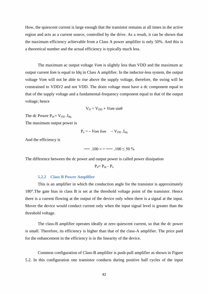
Citation preview
1
DESIGN OF ZIGBEE TRANSMITTER FOR IEEE
802.15.4 STANDARD
A THESIS SUBMITTED IN PARTIAL FULFILMENT OF THE
REQUIRMENTS FOR THE
DEGREE OF
MASTER OF TECHNOLOGY
IN
VLSI DESIGN AND EMBEDDED SYSTEMS
By
JOSHNA PALEPU
Roll No: 209EC2131
DEPARTMENT OF ELECTRONICS AND COMMUNICATION
ENGINEERING
NATIONAL INSTITUTE OF TECHNOLOGY
ROURKELA, ODISHA
INDIA
2011
i
DESIGN OF ZIGBEE TRANSMITTER FOR IEEE
802.15.4 STANDRAD
A THESIS SUBMITTED IN PARTIAL FULFILMENT OF THE
REQUIRMENTS FOR THE
DEGREE OF
MASTER OF TECHNOLOGY
IN
VLSI DESIGN AND EMBEDDED SYSTEMS
BY
JOSHNA PALEPU
Roll No: 209EC2131
UNDER THE GUIDANCE OF
Prof. KAMALAKANTA MAHAPATRA
DEPARTMENT OF ELECTRONICS AND COMMUNICATION
ENGINEERING
NATIONAL INSTITUTE OF TECHNOLOGY
ROURKELA, ODISHA,
INDIA
2011
ii
NATIONAL INSTITUTE OF TECHNOLOGY
ROURKELA
CERTIFICATE
This is to certify that the thesis entitled, “DESIGN OF ZIGBEE TRANSMITTER FOR
IEEE 802.15.4 STANDRAD” submitted by JOSHNA PALEPU Roll no: 209EC2131 in
partial fulfilment of the requirements for the award of Master of Technology Degree in
Electronics & Communication Engineering with specialization in VLSI Design and
Embedded Systems during 2010-2011 at the National Institute of Technology, Rourkela
(Deemed University) is an authentic work carried out by her under my supervision and
guidance. To the best of my knowledge, the matter embodied in the thesis has not been
submitted to any other University / Institute for the award of any Degree or Diploma.
DATE Prof.KAMALAKANTA MAHAPATRA
(Supervisor)
Dept. of Electronics & Communication Engg.
National Institute of Technology
Rourkela-769008

iii
ACKNOWLEDGEMENTS
I am deeply indebted to Prof. KAMALAKANTA MOHAPATRA Dept. of E&CE, my
supervisor on this project, for consistently providing me with the required guidance to help me in the
timely and successful completion of this project. In spite of his extremely busy schedules in
Department, he was always available to share with me his deep insights, wide knowledge and
extensive experience.
I would like to express my gratitude to the following members Mr M. Madhav Kumar, Sc-
D, Mrs Nalini Vidhulatha, Sc-C, Mr Dinesh Kumar of ANURAG Lab, DRDO for giving sufficient
guidance for completing the project.
I would like to express my humble respects to Prof. Sarat Kumar Patra HOD Dept. of
E&CE, Prof. D.P.Acharya, Prof.N.V.L.N Murthy, for teaching me and also helping me how to
learn.
I would like to thank my institution and all the faculty members of ECE Department for their
help and guidance. They have been great sources of inspiration to me and I thank them from the
bottom of my heart.
I would like to thank all my friends and especially my classmates for all the
thoughtful and mind stimulating discussions we had, which prompted us to think beyond the
obvious. I’ve enjoyed their companionship so much during my stay at NIT Rourkela.
I would to like to extend my heartfelt appreciation to my parents, my uncle V.Ananda
Rao and well wishers for their understanding and constant support in this academic pursuits.
Last but not least, I would like to give thanks to my personal Savior, Jesus Christ,
who has given me strength and wisdom to overcome all the difficulties in my life. Without
His guidance, love and promise, I would not have had the courage to purse graduate studies.
iv
Abstract
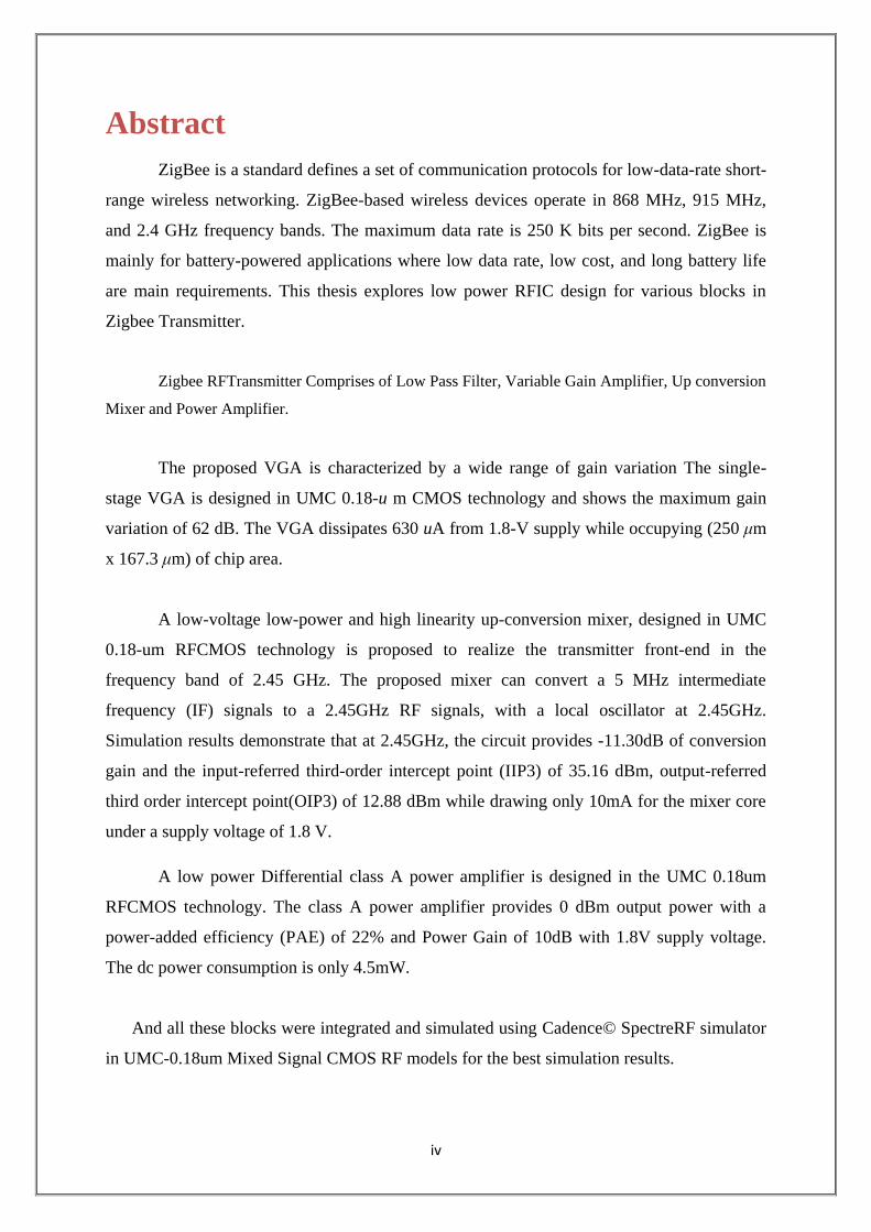
ZigBee is a standard defines a set of communication protocols for low-data-rate short-
range wireless networking. ZigBee-based wireless devices operate in 868 MHz, 915 MHz,
and 2.4 GHz frequency bands. The maximum data rate is 250 K bits per second. ZigBee is
mainly for battery-powered applications where low data rate, low cost, and long battery life
are main requirements. This thesis explores low power RFIC design for various blocks in
Zigbee Transmitter.
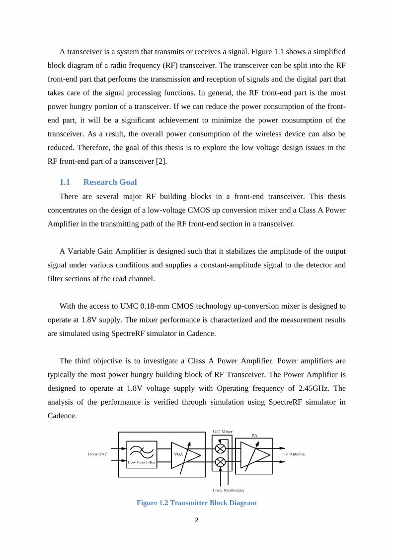
Zigbee RFTransmitter Comprises of Low Pass Filter, Variable Gain Amplifier, Up conversion
Mixer and Power Amplifier.
The proposed VGA is characterized by a wide range of gain variation The single-
stage VGA is designed in UMC 0.18-u m CMOS technology and shows the maximum gain
variation of 62 dB. The VGA dissipates 630 uA from 1.8-V supply while occupying (250 μm
x 167.3 μm) of chip area.
A low-voltage low-power and high linearity up-conversion mixer, designed in UMC
0.18-um RFCMOS technology is proposed to realize the transmitter front-end in the
frequency band of 2.45 GHz. The proposed mixer can convert a 5 MHz intermediate
frequency (IF) signals to a 2.45GHz RF signals, with a local oscillator at 2.45GHz.
Simulation results demonstrate that at 2.45GHz, the circuit provides -11.30dB of conversion
gain and the input-referred third-order intercept point (IIP3) of 35.16 dBm, output-referred
third order intercept point(OIP3) of 12.88 dBm while drawing only 10mA for the mixer core
under a supply voltage of 1.8 V.
A low power Differential class A power amplifier is designed in the UMC 0.18um
RFCMOS technology. The class A power amplifier provides 0 dBm output power with a
power-added efficiency (PAE) of 22% and Power Gain of 10dB with 1.8V supply voltage.
The dc power consumption is only 4.5mW.
And all these blocks were integrated and simulated using Cadence© SpectreRF simulator
in UMC-0.18um Mixed Signal CMOS RF models for the best simulation results.

v
Contents
Abstract ..................................................................................................................................... iv
LIST OF FIGURES ............................................................................................................... viii
LIST OF TABLES .................................................................................................................... xi
Chapter-1.................................................................................................................................... 1
Introduction ................................................................................................................................ 1
Introduction ............................................................................................................................ 1
1.1 Research Goal ............................................................................................................. 2
1.2 Thesis outline .............................................................................................................. 3
Chapter-2.................................................................................................................................... 4
Radio Transceiver Architectures ................................................................................................ 4
2.1 Radio Transceiver Architectures ................................................................................. 4
2.1.1 Superheterodyne receiver ..................................................................................... 5
2.1.2 Low IF receiver .................................................................................................... 6
2.1.3 Direct Conversion receiver .................................................................................. 6
2.2 Transmitter Architectures ............................................................................................ 9
2.2.1 Direct Conversion Architecture ........................................................................... 9
2.2.2 Two Step Architecture ....................................................................................... 11
2.3 Design of Zigbee Transmitter ................................................................................... 12
2.3.1 Specifications for the IEEE 802.15.4 RF Frontend ........................................... 13
Chapter-3.................................................................................................................................. 15
Design of a Variable Gain Amplifier ....................................................................................... 15
3.1 Introduction ............................................................................................................... 15
3.2 Decibel Linear Function ............................................................................................ 16
3.3 Variable Gain Amplifier Design ............................................................................... 17
3.3.1 Control Circuit Block ......................................................................................... 18
3.3.2 Amplifier Block ................................................................................................. 19
vi
3.3.3 Buffer Block....................................................................................................... 21
3.4 The Single Stage Overall VGA ................................................................................. 21
3.5 Results and Discussion .............................................................................................. 22
3.5.1 Layout Issues ..................................................................................................... 25
Chapter-4.................................................................................................................................. 28
Design of a Up-Conversion Mixer ........................................................................................... 28
4.1 Introduction ............................................................................................................... 28
4.2 Mixer Topology ......................................................................................................... 29
4.2.1 Gilbert Cell......................................................................................................... 29
4.3 Performance Parameters ............................................................................................ 30
4.3.1 Conversion Gain ................................................................................................ 30
4.3.2 Gain Compression .............................................................................................. 31
4.3.3 Third order Intermodulation Distortion ............................................................. 32
4.4 Proposed up conversion mixer for High Linearity .................................................... 34
4.4.1 Circuit Operation ............................................................................................... 35
4.5 Results and Discussion .............................................................................................. 36
Chapter-5.................................................................................................................................. 40
Design of a Power Amplifier ................................................................................................... 40
5.1 Introduction ............................................................................................................... 40
5.2 RF Power Amplifier Classification ........................................................................... 41
5.2.1 Class A Power Amplifier ................................................................................... 41
5.2.2 Class B Power Amplifier ................................................................................... 42
5.2.3 Class AB Power Amplifier ................................................................................ 43
5.2.4 Class C Power Amplifier ................................................................................... 44
5.2.5 Class D Power Amplifier ................................................................................... 45
5.2.6 Class E Power Amplifier ................................................................................... 46
5.2.7 Class F Power Amplifier .................................................................................... 47
vii
5.3 Performance Parameters ............................................................................................ 48
5.3.1 Power Added Efficiency .................................................................................... 48
5.3.2 Power Gain......................................................................................................... 49
5.3.2.1 Operating Power Gain........................................................................................ 49
5.3.2.2 Transducer Power Gain ...................................................................................... 49
5.3.2.3 Available Power Gain ........................................................................................ 49
5.3.3 One dB Compression Point ................................................................................ 50
5.4 Impedance Matching Network .................................................................................. 50
5.4.1 L Section Matching Network ............................................................................. 51
5.4.2 T Section Matching Network ............................................................................. 51
5.4.3 π Section Matching Network ............................................................................. 52
5.5 Proposed Differential Class A Power Amplifier ....................................................... 52
5.5.1 Circuit Operation ............................................................................................... 53
5.6 Results and Discussion .............................................................................................. 56
5.6.1 Layout Issues ..................................................................................................... 59
Chapter-6.................................................................................................................................. 63
Design of a Zigbee RFTransmitter .......................................................................................... 63
6.1 Design of a Zigbee RFTransmitter ............................................................................ 63
6.2 Results and Discussion .............................................................................................. 64
Chapter-7.................................................................................................................................. 66
Conclusion and Future Research ............................................................................................. 66
7.1 Conclusion ................................................................................................................. 66
7.2 Future Research ......................................................................................................... 66
REFERENCES: ....................................................................................................................... 67
viii
LIST OF FIGURES
FIGURE 1.1 SIMPLIFIED BLOCK DIAGRAM OF RADIO FREQUENCY TRANSCEIVER ....................... 1
FIGURE 1.2 RFTRANSMITTER BLOCK DIAGRAM ......................................................................... 2
FIGURE 2.1 BLOCK DIAGRAM OF SUPERHETERODYNE RECEIVER ............................................... 5
FIGURE 2. 2 BLOCK DIAGRAM OF DIRECT CONVERSION RECEIVER ............................................ 8
FIGURE 2. 3 BLOCK DIAGRAM OF DIRECT CONVERSION TRANSMITTER ...................................... 9
FIGURE 2. 4 LO PULLING BY PA ................................................................................................. 9
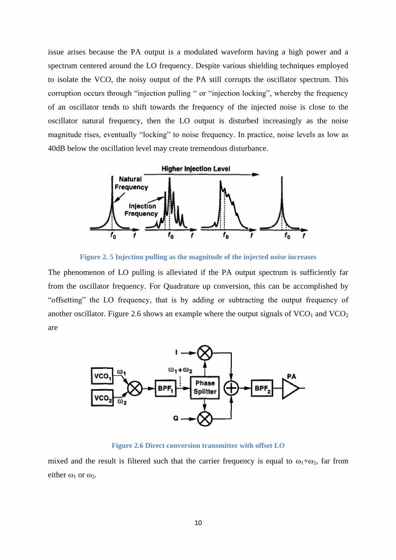
FIGURE 2. 5 INJECTION PULLING AS THE MAGNITUDE OF THE INJECTED NOISE INCREASES ........ 10
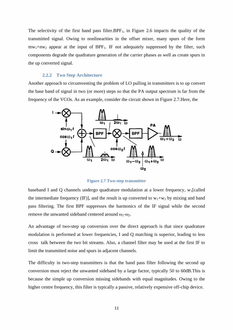
FIGURE 2. 6 DIRECT CONVERSION TRANSMITTER WITH OFFSET LO ........................................... 10
FIGURE 2. 7 TWO-STEP TRANSMITTER ....................................................................................... 11
FIGURE 2. 8 RF FRONT END FOR IEEE 802.15.4 ....................................................................... 12
FIGURE 2. 9 ZIGBEE TRANSMITTER ARCHITECTURE ................................................................... 13
FIGURE 3. 1 (A) DIGITAL CONTROLLED VGA, (B) ANALOG CONTROLLED VGA ...................... 15
FIGURE 3. 2 DECIBEL SCALE PLOTS OF (1), (2) AND THE IDEAL EXPONENTIAL FUNCTION .......... 17
FIGURE 3. 3 : DECIBEL SCALE PLOTS OF (3) FOR VARIOUS VALUES OF K .................................... 17
FIGURE 3. 4 BLOCK DIAGRAM OF TWO STAGE VARIABLE GAIN AMPLIFIER ............................. 18
FIGURE 3. 5 SCHEMATIC OF CONTROL STAGE ........................................................................... 18
FIGURE 3. 6 SCHEMATIC OF AMPLIFIER STAGE ......................................................................... 20
FIGURE 3. 7 SCHEMATIC OF BUFFER STAGE .............................................................................. 21
FIGURE 3. 8 SCHEMATIC OF SINGLE STAGE OVERALL VGA ..................................................... 21
FIGURE 3. 9 FREQUENCY VERSUS GAIN FOR VARIOUS CONTROL VOLTAGES ............................ 23
FIGURE 3. 10 SCHEMATIC OF PROPOSED VGA SETUP ............................................................... 24
FIGURE 3. 11 ANALOG DESIGN ENVIRONMENT FOR VGA SETUP ............................................. 24
FIGURE 3. 12 LAYOUT OF SINGLE STAGE VARIABLE GAIN AMPLIFIER ....................................... 25
FIGURE 3. 13 CONFIG WINDOW OF VGA FOR ANALOG EXTRACTED VIEW ............................... 26
FIGURE 3. 14 POST-LAYOUT SIMULATIONS FOR VGA .............................................................. 26
FIGURE 4. 1 ZIGBEE RFTRANSMITTER ARCHITECTURE ............................................................. 28
FIGURE 4. 2 SCHEMATIC OF CONVENTIONAL GILBERT MIXER .................................................. 29
FIGURE 4. 3 GRAPHICAL REPRESENTATION OF INPUT 1DB COMPRESSION POINT OF MIXER ...... 31
FIGURE 4. 4 FREQUENCY SPECTRUM AT INPUT AND OUTPUT PORT OF MIXER ............................ 32
FIGURE 4. 5 GRAPHICAL REPRESENTATION OF INPUT THIRD ORDER INTERCEPT POINT IIP3 ...... 33
FIGURE 4. 6 SCHEMATIC OF PROPOSED UP CONVERSION MIXER SETUP .................................... 34
FIGURE 4. 7 SCHEMATIC OF PROPOSED UP CONVERSION MIXER .............................................. 35

ix
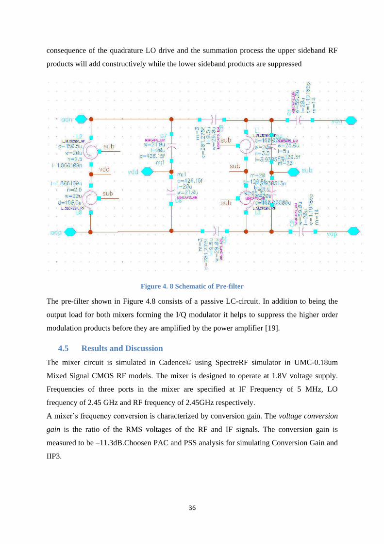
FIGURE 4. 8 SCHEMATIC OF PRE-FILTER.................................................................................... 36
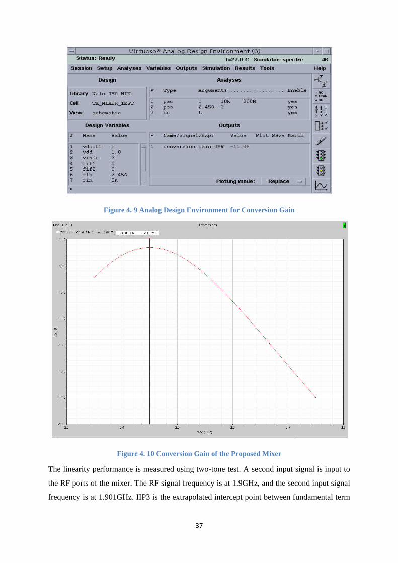
FIGURE 4. 9 ANALOG DESIGN ENVIRONMENT FOR CONVERSION GAIN ..................................... 37
FIGURE 4. 10 CONVERSION GAIN OF THE PROPOSED MIXER ..................................................... 37
FIGURE 4. 11 IIP3 AND OIP3 OF THE PROPOSED MIXER ........................................................... 38
FIGURE 4. 12 TRANSIENT VOLTAGE OF INPUT IF, LO, PRE-FILTER OUTPUT, OUTPUT OF THE
MIXER ................................................................................................................................ 39
FIGURE 5. 1 (A) CLASS A POWER AMPLIFIER, (B) BIASING FOR CLASS A POWER AMPLIFIER ... 41
FIGURE 5. 2 (A) CLASS B STAGE USING TRANSFORMER, (B) BIASING FOR CLASS B AMPLIFIER . 43
FIGURE 5. 3 BIASING FOR CLASS AB AMPLIFIER ....................................................................... 44
FIGURE 5. 4 (A) CLASS C STAGE , (B) BIASING FOR CLASS C AMPLIFIER ................................... 44
FIGURE 5. 5 (A) CLASS D STAGE, (B) CLASS D VOLTAGE AND CURRENT WAVEFORMS ............. 46
FIGURE 5. 6 (A) CLASS E STAGE , (B) CLASS E VOLTAGE AND CURRENT WAVEFORMS ............. 46
FIGURE 5. 7 (A) CLASS F STAGE , (B) CLASS F VOLTAGE AND CURRENT WAVEFORMS ............. 47
FIGURE 5. 8 GAIN COMPRESSION PLOT ..................................................................................... 50
FIGURE 5. 9 BLOCK DIAGRAM OF AMPLIFIER WITH MATCHING NETWORKS .............................. 50
FIGURE 5. 10 L SECTION MATCHING NETWORK ......................................................................... 51
FIGURE 5. 11 T SECTION MATCHING NETWORK ......................................................................... 51
FIGURE 5. 12 Π SECTION MATCHING NETWORK ......................................................................... 52
FIGURE 5. 13 SCHEMATIC OF SINGLE ENDED CASCODE CLASS A POWER AMPLIFIER ............... 53
FIGURE 5. 14 SCHEMATIC OF BIASING CIRCUIT FOR CLASS A POWER AMPLIFIER ..................... 54
FIGURE 5. 15 SCHEMATIC OF DIFFERENTIAL CLASS A POWER AMPLIFIER ................................ 55
FIGURE 5. 16 SCHEMATIC OF DIFFERENTIAL CLASS A POWER AMPLIFIER SETUP ..................... 56
FIGURE 5. 17 ANALOG DESIGN ENVIRONMENT OF DIFFERENTIAL CLASS A POWER AMPLIFIER
SETUP ................................................................................................................................ 56
FIGURE 5. 18 TRANSDUCER POWER GAIN OF DIFFERENTIAL CLASS A POWER AMPLIFIER ....... 57
FIGURE 5. 19 AVAILABLE POWER GAIN OF DIFFERENTIAL CLASS A POWER AMPLIFIER .......... 57
FIGURE 5. 20 OPERATING POWER GAIN OF DIFFERENTIAL CLASS A POWER AMPLIFIER .......... 58
FIGURE 5. 21 INPUT AND OUTPUT TRANSIENT VOLTAGE OF DIFFERENTIAL CLASS A POWER
AMPLIFIER ......................................................................................................................... 58
FIGURE 5. 22 S-PARAMETERS OF DIFFERENTIAL CLASS A POWER AMPLIFIER ......................... 59
FIGURE 5. 23 LAYOUT OF DIFFERENTIAL CLASS A POWER AMPLIFIER ..................................... 60
FIGURE 5. 24 CONFIG WINDOW OF DIFFERENTIAL CLASS A PA FOR ANALOG EXTRACTED VIEW
.......................................................................................................................................... 61
FIGURE 5. 25 POST-LAYOUT SIMULATION OF DIFFERENTIAL CLASS A POWER AMPLIFIER ....... 61

x
FIGURE 6. 1 SCHEMATIC OF ZIGBEE RFTRANSMITTER .............................................................. 63
FIGURE 6. 2 TRANSIENT VOLTAGE OF IN PHASE AND QUADRATURE PHASE COMPONENTS OF VIN,
LPF OUTPUT, VGA OUTPUT/MIXER INPUT. ....................................................................... 64
FIGURE 6. 3 TRANSIENT VOLTAGE OF IN PHASE AND QUADRATURE PHASE COMPONENTS OF
VLO, OUTPUT OF MIXER, POWER AMPLIFIER INPUT, POWER AMPLIFIER OUTPUT AND
ZIGBEE TRANSMITTER OUTPUT .......................................................................................... 65

xi
LIST OF TABLES
TABLE 2. 1 SPECIFICATION OF ZIGBEE TECHNOLOGY ................................................................ 13
TABLE 3. 1 VCONTROL VERSUS VGA OUTPUT (GAIN DB) ......................................................... 22
TABLE 4. 1 SUMMARY OF LINEARITY IMPROVED MIXER PERFORMANCE .................................... 39
TABLE 5. 1 THE PERFORMANCE SUMMARY OF PROPOSED DIFFERENTIAL CLASS A POWER
AMPLIFIER ......................................................................................................................... 62
1
Chapter-1
Introduction
Introduction
In past decades, the tremendous growth in wireless communication systems has given
push to the development of low power radio frequency integrated circuits (RFICs). Power
consumption of a RFIC design has become a major concern due to battery lifetime
consideration. Therefore, a single battery solution becomes very attractive for commercial
and industrial purposes.
In recent years, down-scaling in CMOS advanced technologies has provided high
performance in digital circuits and inexpensive cost to meet the increasing demand of
wireless communication products. With this technology advancement, the unity-current gain
frequency (fT) of CMOS technology is now over several tens of GHz and this makes the
realization of system-on-chip solution possible to further reduce the cost. The demand of
highly integrated CMOS RF building blocks with low power consumption has driven our
research initiatives to explore an area of low power CMOS RFIC designs for applications in a
RF front-end transceiver [1].
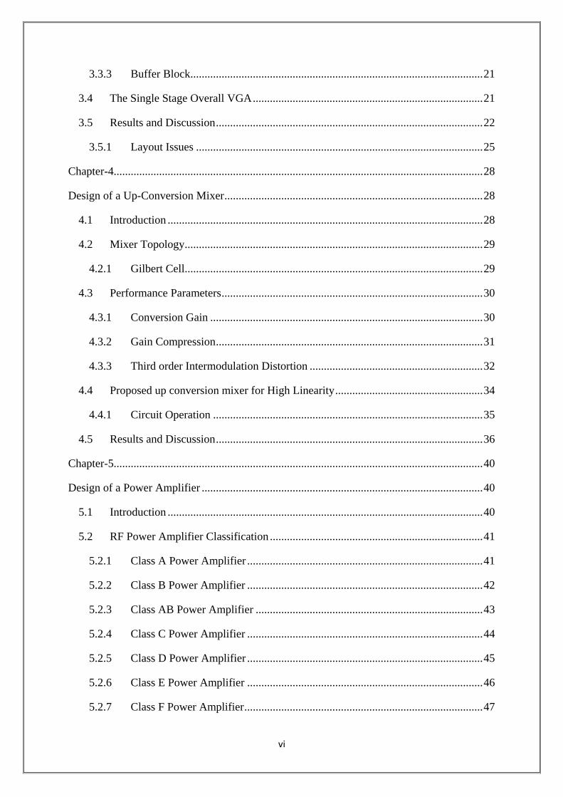
Figure 1.1 Simplified Block Diagram of Radio Frequency Transceiver
2
A transceiver is a system that transmits or receives a signal. Figure 1.1 shows a simplified
block diagram of a radio frequency (RF) transceiver. The transceiver can be split into the RF
front-end part that performs the transmission and reception of signals and the digital part that
takes care of the signal processing functions. In general, the RF front-end part is the most
power hungry portion of a transceiver. If we can reduce the power consumption of the front-
end part, it will be a significant achievement to minimize the power consumption of the
transceiver. As a result, the overall power consumption of the wireless device can also be
reduced. Therefore, the goal of this thesis is to explore the low voltage design issues in the
RF front-end part of a transceiver [2].
1.1 Research Goal
There are several major RF building blocks in a front-end transceiver. This thesis
concentrates on the design of a low-voltage CMOS up conversion mixer and a Class A Power
Amplifier in the transmitting path of the RF front-end section in a transceiver.
A Variable Gain Amplifier is designed such that it stabilizes the amplitude of the output
signal under various conditions and supplies a constant-amplitude signal to the detector and
filter sections of the read channel.
With the access to UMC 0.18-mm CMOS technology up-conversion mixer is designed to
operate at 1.8V supply. The mixer performance is characterized and the measurement results
are simulated using SpectreRF simulator in Cadence.
The third objective is to investigate a Class A Power Amplifier. Power amplifiers are
typically the most power hungry building block of RF Transceiver. The Power Amplifier is
designed to operate at 1.8V voltage supply with Operating frequency of 2.45GHz. The
analysis of the performance is verified through simulation using SpectreRF simulator in
Cadence.
Figure 1.2 Transmitter Block Diagram
3
1.2 Thesis outline
This thesis is divided into seven chapters. It is organized in such way as to properly
layout the detail investigations and results of the research work.
The motivation and research goal are presented in Chapter 1 with a summary of the thesis
outline.
Chapter 2 is an overview on modern radio receivers. A general background on
different types of receiver architectures are presented. The state-of-the-art of these
architectures is reviewed.
Chapter 3 provides a background theory review of the variable gain amplifier and the
circuit design details of variable gain amplifier and concluded with the post layout
simulations.
Chapter 4 provides a background theory review of the up-conversion mixer operation.
The fundamentals and parameters of performance are discussed and followed by the circuit
design details of mixer .The chapter is concluded with simulation results.
Chapter 5 starts with a background theory review of the Power amplifier and their
classifications followed by the circuit design description of the Class A power amplifier.
Simulation results of class A power amplifier are provided to verify the performance analysis.
This chapter concluded with the post layout simulation of Class A power amplifier
Chapter 6 starts with the design of the zigbee transmitter and concludes with the
simulation results.
Conclusion and future work of this thesis are presented in Chapter 7.
4
Chapter-2
Radio Transceiver Architectures
2.1 Radio Transceiver Architectures
Primary criteria in selecting Transceiver Architectures [3]:
Complexity
Cost
Power dissipation
No. of external components
The first consideration in designing an RFIC is the system architecture and its frequency
plan. Architecture is determined by choosing among different possible ones:
Superheterodyne using one or several IF stages
Direct conversion
Low IF
By frequency plan, it means the intermediate frequency/frequencies choice (Not Applicable
for direct conversion architecture), with considerations on image interference avoidance,
blockers, and RF leakage/isolation analysis, DC-offset issue, I/Q imbalance issue, etc.
Frequency plan specification impacts on system noise, interference, and distortion analysis.
In a generalized sense, special issues associated with chosen RF transceiver architecture are
addressed in frequency plan specification.
For direct conversion, the following issues are important:
- DC offset or order-two products
- 1/f or flicker noise
- I/Q imbalance impacts
- etc.
5
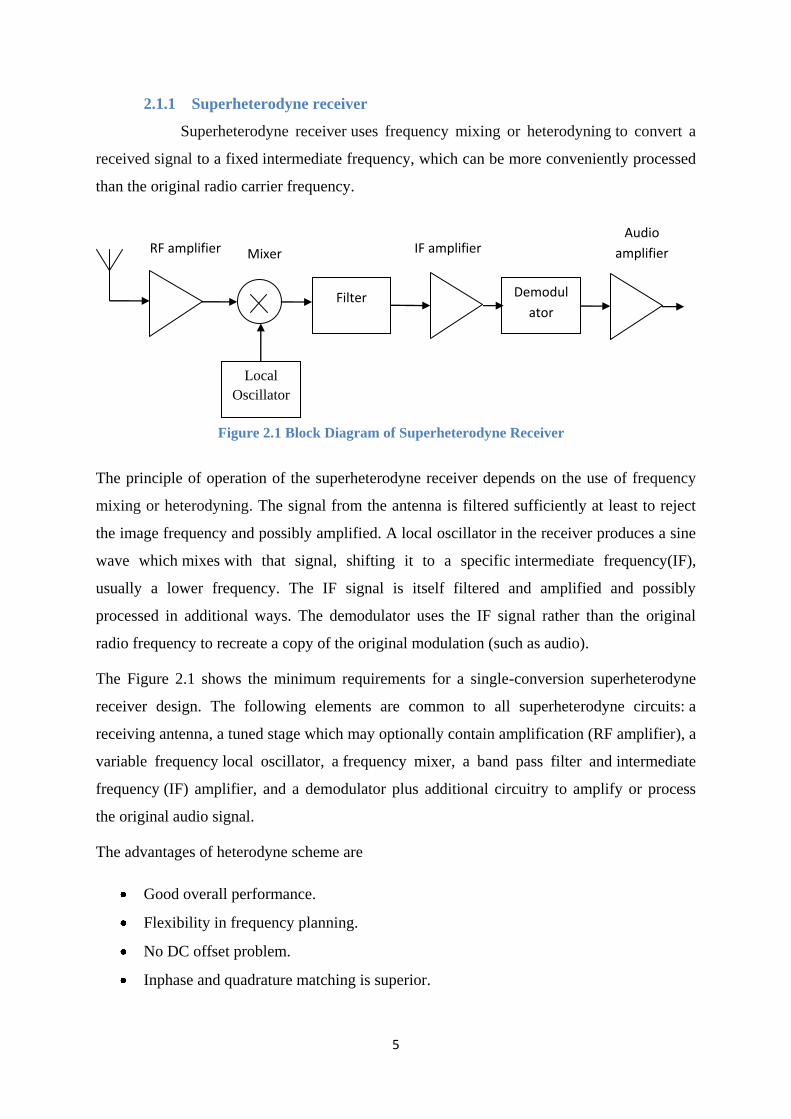
2.1.1 Superheterodyne receiver
Superheterodyne receiver uses frequency mixing or heterodyning to convert a
received signal to a fixed intermediate frequency, which can be more conveniently processed
than the original radio carrier frequency.
The principle of operation of the superheterodyne receiver depends on the use of frequency
mixing or heterodyning. The signal from the antenna is filtered sufficiently at least to reject
the image frequency and possibly amplified. A local oscillator in the receiver produces a sine
wave which mixes with that signal, shifting it to a specific intermediate frequency(IF),
usually a lower frequency. The IF signal is itself filtered and amplified and possibly
processed in additional ways. The demodulator uses the IF signal rather than the original
radio frequency to recreate a copy of the original modulation (such as audio).
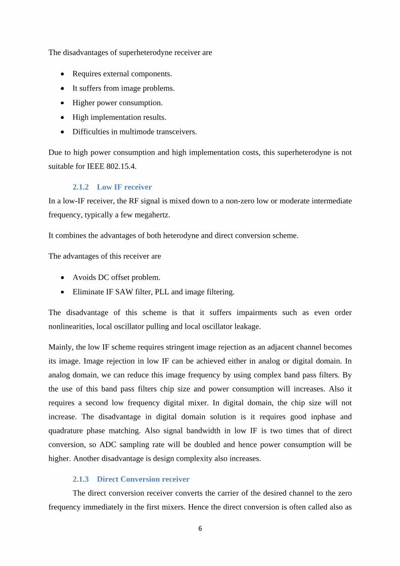
The Figure 2.1 shows the minimum requirements for a single-conversion superheterodyne
receiver design. The following elements are common to all superheterodyne circuits: a
receiving antenna, a tuned stage which may optionally contain amplification (RF amplifier), a
variable frequency local oscillator, a frequency mixer, a band pass filter and intermediate
frequency (IF) amplifier, and a demodulator plus additional circuitry to amplify or process
the original audio signal.
The advantages of heterodyne scheme are
Good overall performance.
Flexibility in frequency planning.
No DC offset problem.
Inphase and quadrature matching is superior.
Filter Demodul
ator
Local
Oscillator
RF amplifier Mixer IF amplifier Audio
amplifier
Figure 2.1 Block Diagram of Superheterodyne Receiver
6
The disadvantages of superheterodyne receiver are
Requires external components.
It suffers from image problems.
Higher power consumption.
High implementation results.
Difficulties in multimode transceivers.
Due to high power consumption and high implementation costs, this superheterodyne is not
suitable for IEEE 802.15.4.
2.1.2 Low IF receiver
In a low-IF receiver, the RF signal is mixed down to a non-zero low or moderate intermediate
frequency, typically a few megahertz.
It combines the advantages of both heterodyne and direct conversion scheme.
The advantages of this receiver are
Avoids DC offset problem.
Eliminate IF SAW filter, PLL and image filtering.
The disadvantage of this scheme is that it suffers impairments such as even order
nonlinearities, local oscillator pulling and local oscillator leakage.
Mainly, the low IF scheme requires stringent image rejection as an adjacent channel becomes
its image. Image rejection in low IF can be achieved either in analog or digital domain. In
analog domain, we can reduce this image frequency by using complex band pass filters. By
the use of this band pass filters chip size and power consumption will increases. Also it
requires a second low frequency digital mixer. In digital domain, the chip size will not
increase. The disadvantage in digital domain solution is it requires good inphase and
quadrature phase matching. Also signal bandwidth in low IF is two times that of direct
conversion, so ADC sampling rate will be doubled and hence power consumption will be
higher. Another disadvantage is design complexity also increases.
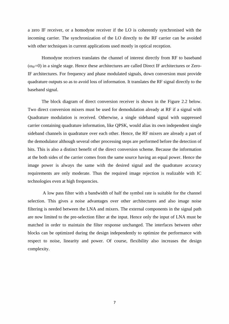
2.1.3 Direct Conversion receiver
The direct conversion receiver converts the carrier of the desired channel to the zero
frequency immediately in the first mixers. Hence the direct conversion is often called also as
7
a zero IF receiver, or a homodyne receiver if the LO is coherently synchronised with the
incoming carrier. The synchronization of the LO directly to the RF carrier can be avoided
with other techniques in current applications used mostly in optical reception.
Homodyne receivers translates the channel of interest directly from RF to baseband
(ωIF=0) in a single stage. Hence these architectures are called Direct IF architectures or Zero-
IF architectures. For frequency and phase modulated signals, down conversion must provide
quadrature outputs so as to avoid loss of information. It translates the RF signal directly to the
baseband signal.
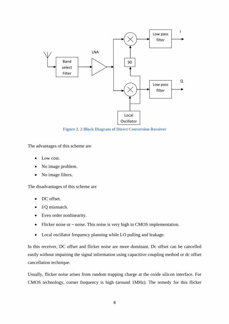
The block diagram of direct conversion receiver is shown in the Figure 2.2 below.
Two direct conversion mixers must be used for demodulation already at RF if a signal with
Quadrature modulation is received. Otherwise, a single sideband signal with suppressed
carrier containing quadrature information, like QPSK, would alias its own independent single
sideband channels in quadrature over each other. Hence, the RF mixers are already a part of
the demodulator although several other processing steps are performed before the detection of
bits. This is also a distinct benefit of the direct conversion scheme. Because the information
at the both sides of the carrier comes from the same source having an equal power. Hence the
image power is always the same with the desired signal and the quadrature accuracy
requirements are only moderate. Thus the required image rejection is realizable with IC
technologies even at high frequencies.
A low pass filter with a bandwidth of half the symbol rate is suitable for the channel
selection. This gives a noise advantages over other architectures and also image noise
filtering is needed between the LNA and mixers. The external components in the signal path
are now limited to the pre-selection filter at the input. Hence only the input of LNA must be
matched in order to maintain the filter response unchanged. The interfaces between other
blocks can be optimized during the design independently to optimize the performance with
respect to noise, linearity and power. Of course, flexibility also increases the design
complexity.
8
The advantages of this scheme are
Low cost.
No image problem.
No image filters.
The disadvantages of this scheme are
DC offset.
I/Q mismatch.
Even order nonlinearity.
Flicker noise or noise. This noise is very high in CMOS implementation.
Local oscillator frequency planning while LO pulling and leakage.
In this receiver, DC offset and flicker noise are more dominant. Dc offset can be cancelled
easily without impairing the signal information using capacitive coupling method or dc offset
cancellation technique.
Usually, flicker noise arises from random trapping charge at the oxide silicon interface. For
CMOS technology, corner frequency is high (around 1MHz). The remedy for this flicker
Band
select
Filter
LNA
I
Q
Local
Oscillator
Low pass
filter
Low pass
filter
900
Figure 2. 2 Block Diagram of Direct Conversion Receiver
9
noise problem is by using passive mixers or by using vertical NPN transistors in CMOS
technology for the switching core of active mixers.
On comparing the three transceiver architectures, we were selected the direct conversion
scheme because of low power consumption, low cost and high integrable chip.
2.2 Transmitter Architectures
The choice of transmitter architecture is determined by two important factors: wanted and
unwanted emission requirement and the number of oscillators and external filters. In general,
the architecture and frequency planning of the transmitter must be selected in conjunction
with those of the receiver so as to allow sharing hardware and possibility power [4].
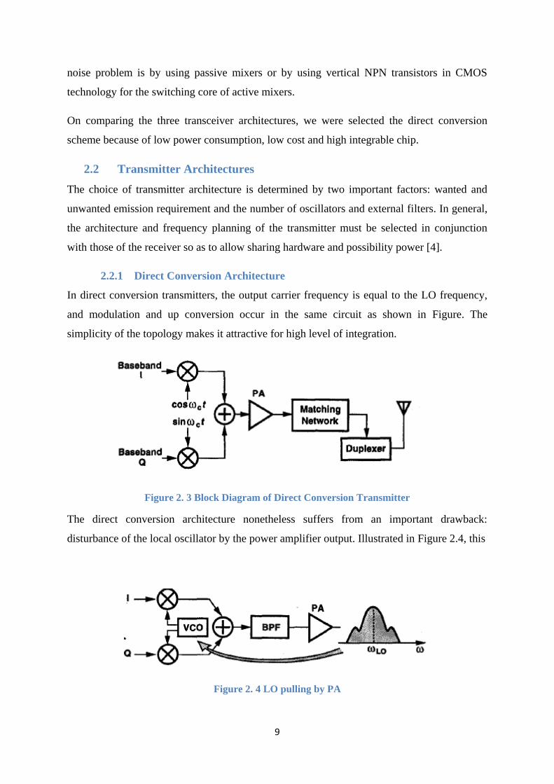
2.2.1 Direct Conversion Architecture
In direct conversion transmitters, the output carrier frequency is equal to the LO frequency,
and modulation and up conversion occur in the same circuit as shown in Figure. The
simplicity of the topology makes it attractive for high level of integration.
Figure 2. 3 Block Diagram of Direct Conversion Transmitter
The direct conversion architecture nonetheless suffers from an important drawback:
disturbance of the local oscillator by the power amplifier output. Illustrated in Figure 2.4, this
Figure 2. 4 LO pulling by PA
10
issue arises because the PA output is a modulated waveform having a high power and a
spectrum centered around the LO frequency. Despite various shielding techniques employed
to isolate the VCO, the noisy output of the PA still corrupts the oscillator spectrum. This
corruption occurs through “injection pulling “ or “injection locking”, whereby the frequency
of an oscillator tends to shift towards the frequency of the injected noise is close to the
oscillator natural frequency, then the LO output is disturbed increasingly as the noise
magnitude rises, eventually “locking” to noise frequency. In practice, noise levels as low as
40dB below the oscillation level may create tremendous disturbance.
Figure 2. 5 Injection pulling as the magnitude of the injected noise increases
The phenomenon of LO pulling is alleviated if the PA output spectrum is sufficiently far
from the oscillator frequency. For Quadrature up conversion, this can be accomplished by
“offsetting” the LO frequency, that is by adding or subtracting the output frequency of
another oscillator. Figure 2.6 shows an example where the output signals of VCO1 and VCO2
are
Figure 2.6 Direct conversion transmitter with offset LO
mixed and the result is filtered such that the carrier frequency is equal to ω1+ω2, far from
either ω1 or ω2.
11
The selectivity of the first band pass filter.BPF1, in Figure 2.6 impacts the quality of the
transmitted signal. Owing to nonlinearities in the offset mixer, many spurs of the form
mw1+nw2 appear at the input of BPF1. IF not adequately suppressed by the filter, such
components degrade the quadrature generation of the carrier phases as well as create spurs in
the up converted signal.
2.2.2 Two Step Architecture
Another approach to circumventing the problem of LO pulling in transmitters is to up convert
the base band of signal in two (or more) steps so that the PA output spectrum is far from the
frequency of the VCOs. As an example, consider the circuit shown in Figure 2.7.Here, the
Figure 2.7 Two-step transmitter
baseband I and Q channels undergo quadrature modulation at a lower frequency, w1[called
the intermediate frequency (IF)], and the result is up converted to w1+w2 by mixing and band
pass filtering. The first BPF suppresses the harmonics of the IF signal while the second
remove the unwanted sideband centered around ω1-ω2.
An advantage of two-step up conversion over the direct approach is that since quadrature
modulation is performed at lower frequencies, I and Q matching is superior, leading to less
cross talk between the two bit streams. Also, a channel filter may be used at the first IF to
limit the transmitted noise and spurs in adjacent channels.
The difficulty in two-step transmitters is that the band pass filter following the second up
conversion must reject the unwanted sideband by a large factor, typically 50 to 60dB.This is
because the simple up conversion missing sidebands with equal magnitudes. Owing to the
higher centre frequency, this filter is typically a passive, relatively expensive off-chip device.
12
2.3 Design of Zigbee Transmitter
CMOS RF Front-end for IEEE 802.15.4
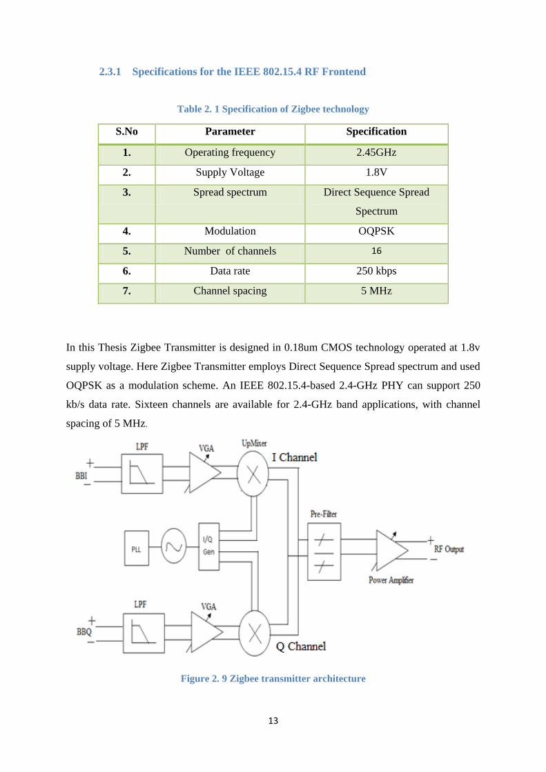
The Architecture of the Zigbee Frontend is shown in Figure 2.8, block diagram is shown in
Figure 2.9.
RF Front-end for IEEE 802.15.4
Architecture:
Figure 2.8 RF Front end for IEEE 802.15.4
IEEE 802.15.4 assigns three frequency bands of operation: the 868-MHz, 915-MHz, and 2.4-
GHz unlicensed industrial, scientific, and medical (ISM) bands. Among the three, the 2.4-
GHz band is highly attractive, since this unlicensed band is commonly available throughout
the world. Typical applications of this low data rate standard include those for industrial and
commercial uses, home automation, PC peripherals, consumer electronics, and personal
health care appliances, as well as for toys and games that should be able to run for six months
to two years on just button cells or batteries[3].
13
2.3.1 Specifications for the IEEE 802.15.4 RF Frontend
Table 2. 1 Specification of Zigbee technology
S.No Parameter Specification
1. Operating frequency 2.45GHz
2. Supply Voltage 1.8V
3. Spread spectrum Direct Sequence Spread
Spectrum
4. Modulation OQPSK
5. Number of channels 16
6. Data rate 250 kbps
7. Channel spacing 5 MHz
In this Thesis Zigbee Transmitter is designed in 0.18um CMOS technology operated at 1.8v
supply voltage. Here Zigbee Transmitter employs Direct Sequence Spread spectrum and used
OQPSK as a modulation scheme. An IEEE 802.15.4-based 2.4-GHz PHY can support 250
kb/s data rate. Sixteen channels are available for 2.4-GHz band applications, with channel
spacing of 5 MHz.
Figure 2. 9 Zigbee transmitter architecture
14
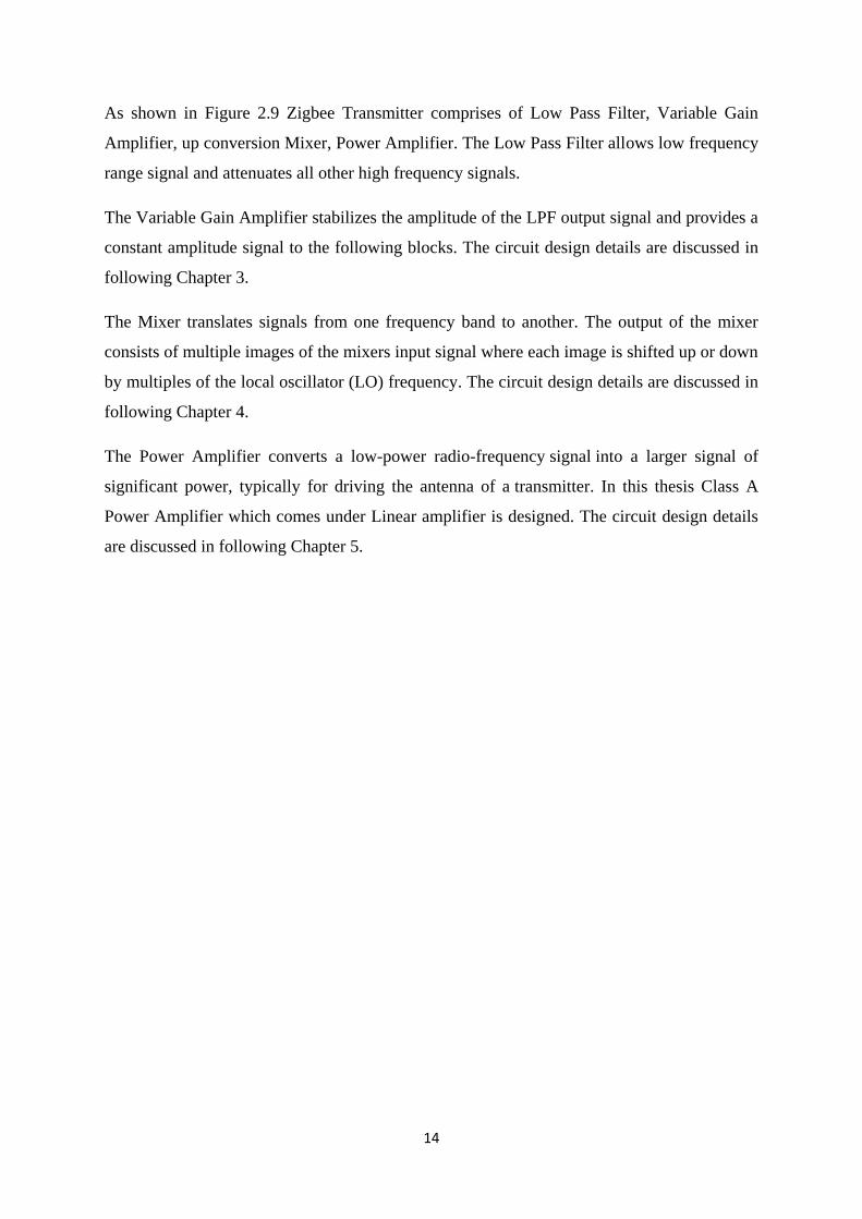
As shown in Figure 2.9 Zigbee Transmitter comprises of Low Pass Filter, Variable Gain
Amplifier, up conversion Mixer, Power Amplifier. The Low Pass Filter allows low frequency
range signal and attenuates all other high frequency signals.
The Variable Gain Amplifier stabilizes the amplitude of the LPF output signal and provides a
constant amplitude signal to the following blocks. The circuit design details are discussed in
following Chapter 3.
The Mixer translates signals from one frequency band to another. The output of the mixer
consists of multiple images of the mixers input signal where each image is shifted up or down
by multiples of the local oscillator (LO) frequency. The circuit design details are discussed in
following Chapter 4.
The Power Amplifier converts a low-power radio-frequency signal into a larger signal of
significant power, typically for driving the antenna of a transmitter. In this thesis Class A
Power Amplifier which comes under Linear amplifier is designed. The circuit design details
are discussed in following Chapter 5.
15
Chapter-3
Design of a Variable Gain Amplifier
3.1 Introduction
VARIABLE gain amplifiers (VGAs) can be found in many applications and are used to
maximize the dynamic range of overall systems in medical equipments, telecommunication
systems, hearing aids, disk drives, and others[5]-[9]. In disk drives and CCD imaging
equipments, the VGAs play the important role of stabilizing the amplitude of the output
signal under various conditions and supply a constant-amplitude signal to the detector and
filter sections of the read channel. The VGA for these applications requires a gain variation
range of more than 30dB. In communication systems, the VGA is normally employed in a
feedback loop to implement an automatic gain control (AGC) amplifier.
The AGC amplifier is a circuit that automatically controls its gain in response to the
amplitude of the input signal, leading to a constant-amplitude output. The gain as an
exponential function of control voltage, which is not an easily obtainable characteristic in
CMOS technology, is desirable for minimizing the settling time of the AGC loops. Moreover,
code-division multiple-access (CDMA) systems require VGAs with high linearity and wide
range of gain variation.
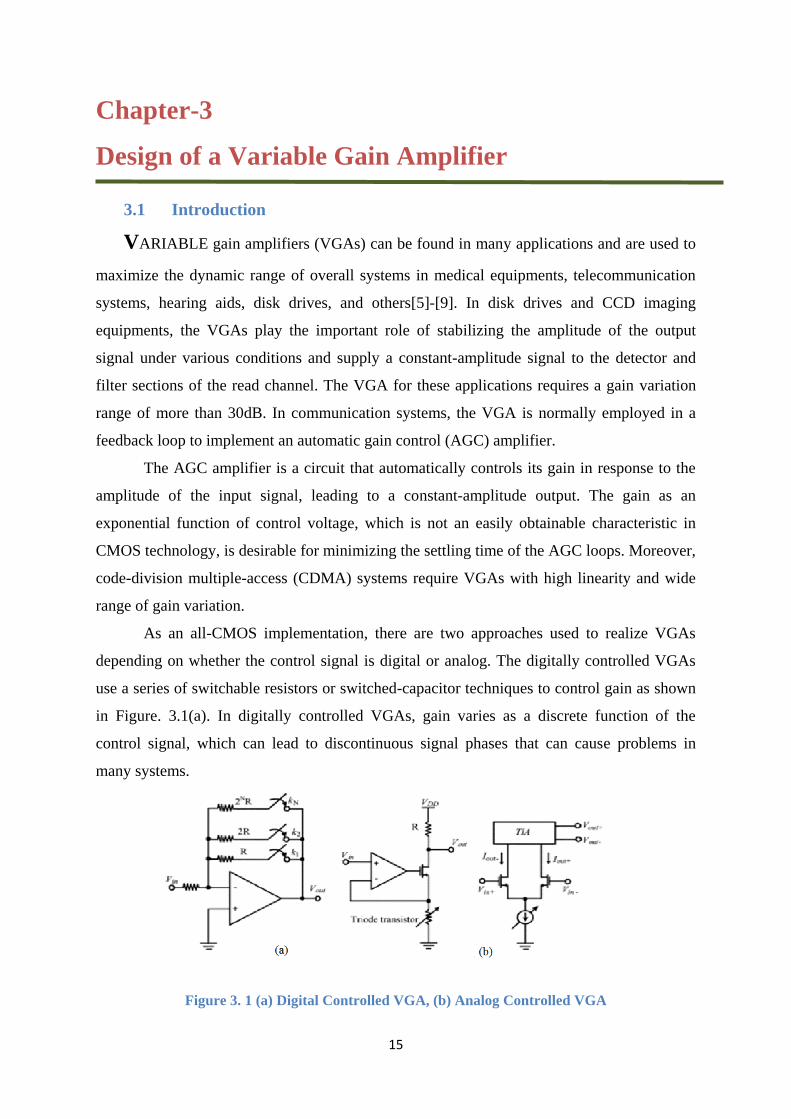
As an all-CMOS implementation, there are two approaches used to realize VGAs
depending on whether the control signal is digital or analog. The digitally controlled VGAs
use a series of switchable resistors or switched-capacitor techniques to control gain as shown
in Figure. 3.1(a). In digitally controlled VGAs, gain varies as a discrete function of the
control signal, which can lead to discontinuous signal phases that can cause problems in
many systems.
Figure 3. 1 (a) Digital Controlled VGA, (b) Analog Controlled VGA
16
In order to reduce the amount of jumps, a large number of control bits are required with
digitally controlled VGAs. Therefore, for applications that require smooth gain transitions,
the VGAs controlled by analog signal are preferred. The VGAs controlled by analog signals
typically adopt variable transconductance or resistance stages for gain variation as shown in
Figure. 3.1(b). With these topologies, the gains can be controlled continuously, but obtaining
a wide exponential gain variation as a function of control voltage is a big issue, especially in
CMOS technology.
In cellular wireless communication systems, the amplitude of the receiver and
transmitter signals varies greatly. For this reason, for example, in a CDMA system, the
transceiver requires at least 80 dB of dynamic gain variation and splits into RF and
IF/baseband stages. In a typical receiver, most of the gain variation is assigned to the
baseband stage. Therefore, to cover such a wide dynamic range, conventional CMOS-based
VGAs require at least 4 or 5 gain-varying stages. The multiple gain-varying stages lead to a
higher amount of power dissipation, larger chip area, and higher cost.
3.2 Decibel Linear Function
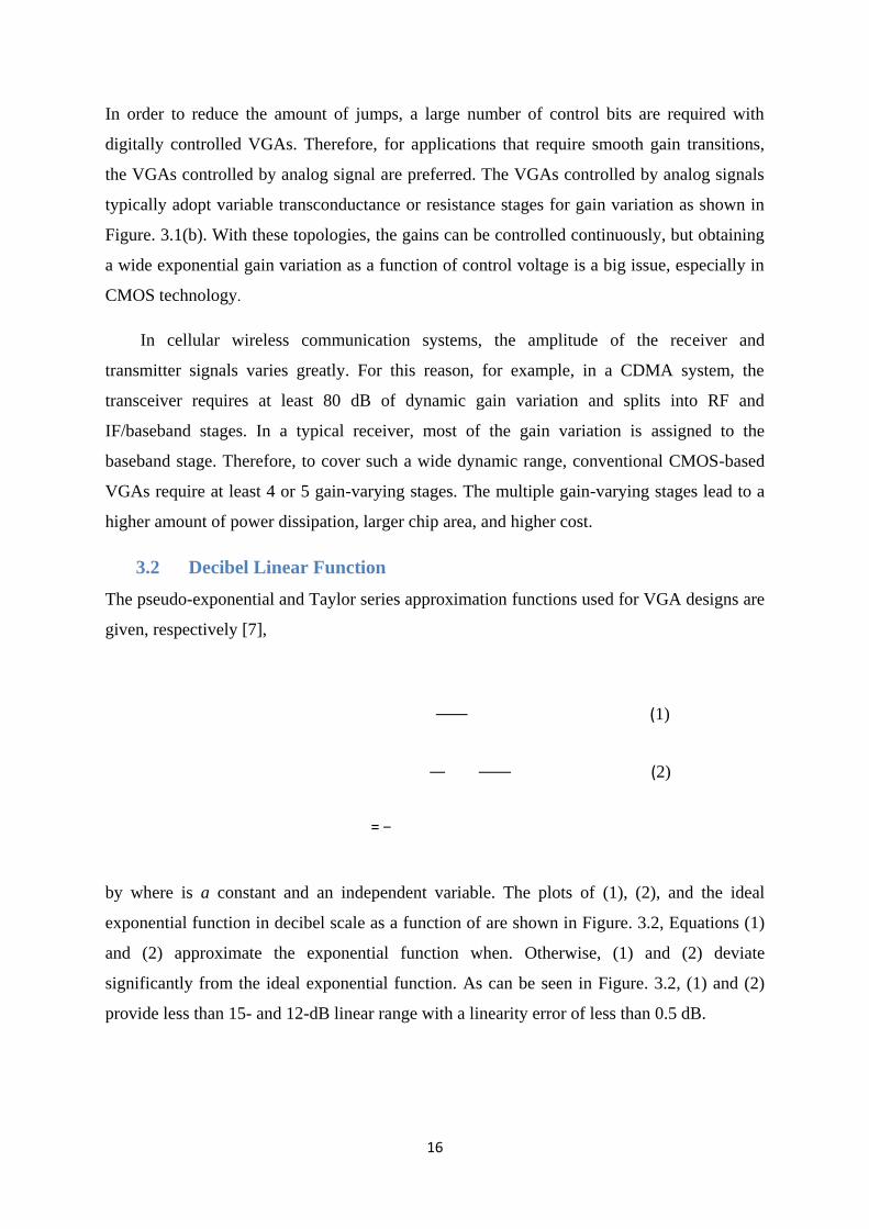
The pseudo-exponential and Taylor series approximation functions used for VGA designs are
given, respectively [7],
(1)
(2)
=
by where is a constant and an independent variable. The plots of (1), (2), and the ideal
exponential function in decibel scale as a function of are shown in Figure. 3.2, Equations (1)
and (2) approximate the exponential function when. Otherwise, (1) and (2) deviate
significantly from the ideal exponential function. As can be seen in Figure. 3.2, (1) and (2)
provide less than 15- and 12-dB linear range with a linearity error of less than 0.5 dB.
17
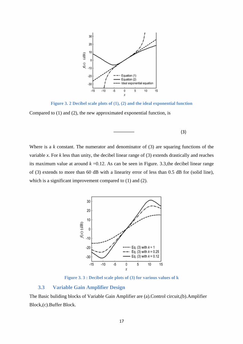
Figure 3. 2 Decibel scale plots of (1), (2) and the ideal exponential function
Compared to (1) and (2), the new approximated exponential function, is
(3)
Where is a k constant. The numerator and denominator of (3) are squaring functions of the
variable x. For k less than unity, the decibel linear range of (3) extends drastically and reaches
its maximum value at around k =0.12. As can be seen in Figure. 3.3,the decibel linear range
of (3) extends to more than 60 dB with a linearity error of less than 0.5 dB for (solid line),
which is a significant improvement compared to (1) and (2).
Figure 3. 3 : Decibel scale plots of (3) for various values of k
3.3 Variable Gain Amplifier Design
The Basic buliding blocks of Variable Gain Amplifier are (a).Control circuit,(b).Amplifier
Block,(c).Buffer Block.
18
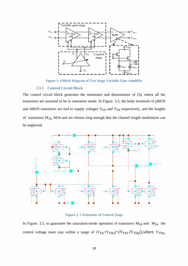
Figure 3. 4 Block Diagram of Two Stage Variable Gain Amplifier
3.3.1 Control Circuit Block
The control circuit block generates the numerator and denominator of (3), where all the
transistors are assumed to be in saturation mode. In Figure. 3.5, the body terminals of pMOS
and nMOS transistors are tied to supply voltages VDD and VSS respectively, and the lengths
of transistors M18, M24 and are chosen long enough that the channel length modulation can
be neglected.
Figure 3. 5 Schematic of Control Stage
In Figure. 3.5, to guarantee the saturation-mode operation of transistors M18 and M24 the
control voltage must stay within a range of (VSS+VTHn)~(VDD-|VTHp|),where VTHn,
19
VTHp are the threshold voltages of nMOS and pMOS transistors, respectively. The drain
currents of transistors M18, M24 in Fig. 3.5 can be given as
= (4)
= (5)
where Kp Kn ,are constants [Kp=(W1/2L1)uP Coxand Kn=(W2/2L2)un Cox ]. In Figure. 3.5,
since the current IC1 and IC2 are ID1+I0 and ID2+I0 respectively, the resulting currents IC1 and
IC2 assuming Kp =Kn=K, VDD =-VSS and |VTHp|= VTHn = VTH ,the ratios of IC1 and IC2 is given
by
= (6)
The VGA that adopts (6) shows a wide range of gain variation however, the required
dynamic gain range for different applications is not equal; therefore, if the VGA provides a
wider range of gain variation than the requirement, then the range of the control signal is
reduced. Consequently, in order to maximize the range of control signal, the gain variation
range of the VGA should be controllable.
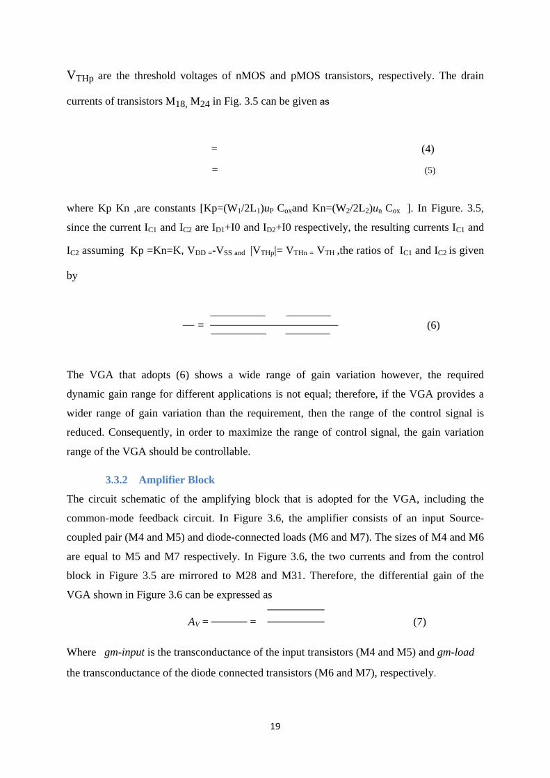
3.3.2 Amplifier Block
The circuit schematic of the amplifying block that is adopted for the VGA, including the
common-mode feedback circuit. In Figure 3.6, the amplifier consists of an input Source-
coupled pair (M4 and M5) and diode-connected loads (M6 and M7). The sizes of M4 and M6
are equal to M5 and M7 respectively. In Figure 3.6, the two currents and from the control
block in Figure 3.5 are mirrored to M28 and M31. Therefore, the differential gain of the
VGA shown in Figure 3.6 can be expressed as
AV = = (7)
Where gm-input is the transconductance of the input transistors (M4 and M5) and gm-load
the transconductance of the diode connected transistors (M6 and M7), respectively.
20
Figure 3. 6 Schematic of Amplifier Stage
From (6) and (7), the differential gain as a function of the control voltage is given by
AV = (8)
From Figure. 3.6, the amplifier gain can be varied by controlling the current through
transistors and M28 and M31. Since the amplifier adopts current sources as active loads, the
currents through transistors M8 and M9 must also vary accordingly. From (6), the sum of the
currents through and is given as
IC1 + IC2 = 2K (1 + ) (9)
which is a second-order polynomial of the control voltage VC . As a result, the drain currents
through transistors M28 and M31 vary as a function of gain variation. Therefore, the strong
common-mode feedback circuit shown in Figure. 3.6 is required in order to prevent any of
the transistors from entering linear mode operation and to maintain a specific dc value for the
biasing of the next stage.
21
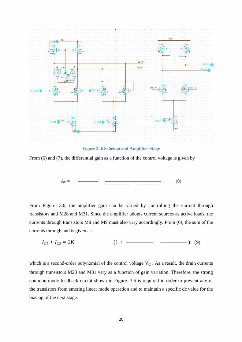
3.3.3 Buffer Block
Figure 3. 7 Schematic of Buffer Stage
The buffer is designed as a differential source follower, in which the gates of the input
different transistors are differential inputs of the buffer with high impedance while the output
impedance can be adjusted to 50Ω by a proper choice of the bias current and the size of input
different transistors of the buffer. The buffer in Figure 3.7 is added for the convenience of
measurements, providing high-input and 50Ω output impedances.
3.4 The Single Stage Overall VGA
Figure 3. 8 Schematic of Single Stage Overall VGA
Regarding the frequency response, assuming that the VGA is evaluated under a 50Ω
environment, the bandwidth of the VGA is dominated by the pole at the input and the inter-
stage node between two amplifiers. The input pole is a function of the input capacitance and
resistance. Due to the Miller effect, the input capacitance is proportional to the amplifier gain;
therefore, the bandwidth is reduced at higher gain settings. The output pole is proportional to
the output capacitance and resistance. Since the resistance from the inter-stage node to the ac
22
ground is dominated by the diode-connected transistors M6 and M7 in Figure 3.6, which vary
as a function of gain, the bandwidth of the amplifier varies accordingly. At higher gains, the
current flowing through the diode-connected transistors is reduced leading to narrower
bandwidths. Since the currents flow through M6 and M7 are squaring functions of the control
voltage, the bandwidth of the VGA varies significantly from low- to high-gain modes.
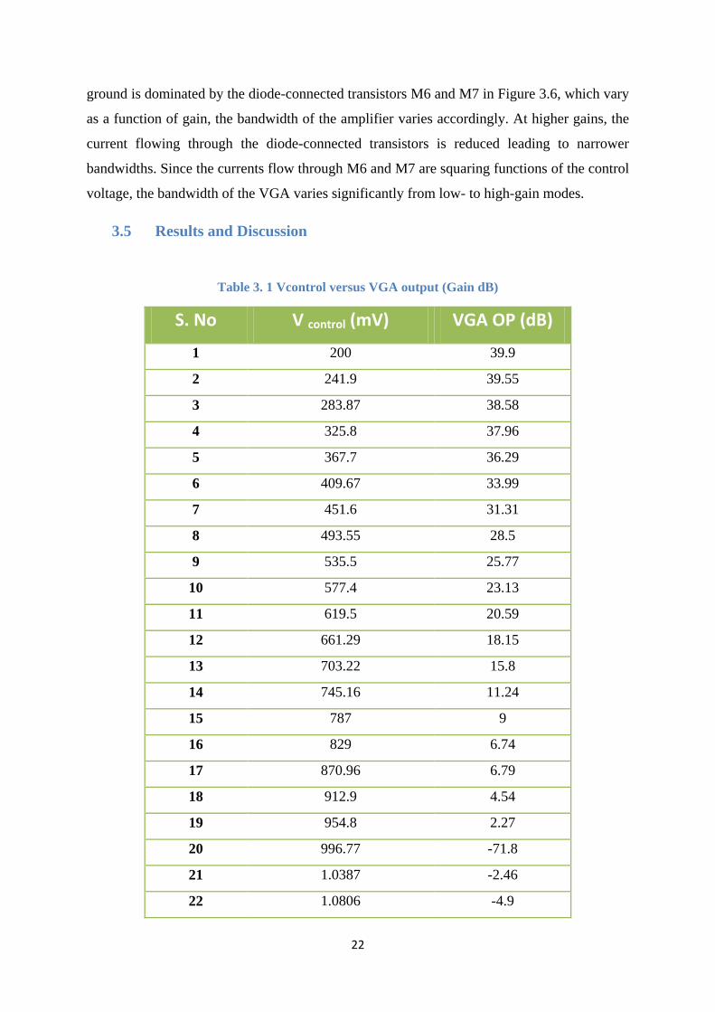
3.5 Results and Discussion
Table 3. 1 Vcontrol versus VGA output (Gain dB)
S. No V control (mV) VGA OP (dB)
1 200 39.9
2 241.9 39.55
3 283.87 38.58
4 325.8 37.96
5 367.7 36.29
6 409.67 33.99
7 451.6 31.31
8 493.55 28.5
9 535.5 25.77
10 577.4 23.13
11 619.5 20.59
12 661.29 18.15
13 703.22 15.8
14 745.16 11.24
15 787 9
16 829 6.74
17 870.96 6.79
18 912.9 4.54
19 954.8 2.27
20 996.77 -71.8
21 1.0387 -2.46
22 1.0806 -4.9
23
23 1.1225 -7.43
24 1.1645 -10.069
25 1.2 -12.5
26 1.248 -15.5
27 1.29 -17.99
28 1.33 -19.845
29 1.374 -20.985
30 1.416 -21.595
31 1.5 -22
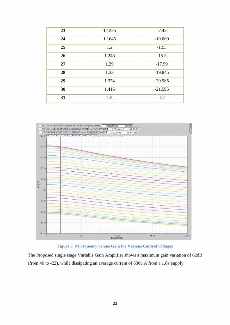
Figure 3. 9 Frequency versus Gain for Various Control voltages
The Proposed single stage Variable Gain Amplifier shows a maximum gain variation of 62dB
(from 40 to -22), while dissipating an average current of 630u A from a 1.8v supply.
24
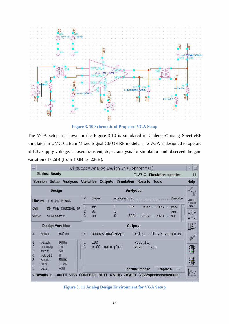
Figure 3. 10 Schematic of Proposed VGA Setup
The VGA setup as shown in the Figure 3.10 is simulated in Cadence© using SpectreRF
simulator in UMC-0.18um Mixed Signal CMOS RF models. The VGA is designed to operate
at 1.8v supply voltage. Chosen transient, dc, ac analysis for simulation and observed the gain
variation of 62dB (from 40dB to -22dB).
Figure 3. 11 Analog Design Environment for VGA Setup
25
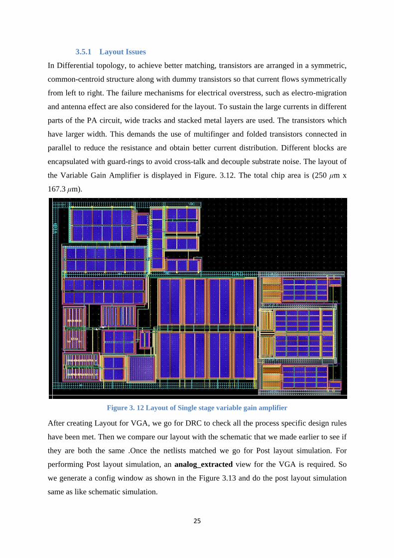
3.5.1 Layout Issues
In Differential topology, to achieve better matching, transistors are arranged in a symmetric,
common-centroid structure along with dummy transistors so that current flows symmetrically
from left to right. The failure mechanisms for electrical overstress, such as electro-migration
and antenna effect are also considered for the layout. To sustain the large currents in different
parts of the PA circuit, wide tracks and stacked metal layers are used. The transistors which
have larger width. This demands the use of multifinger and folded transistors connected in
parallel to reduce the resistance and obtain better current distribution. Different blocks are
encapsulated with guard-rings to avoid cross-talk and decouple substrate noise. The layout of
the Variable Gain Amplifier is displayed in Figure. 3.12. The total chip area is (250 μm x
167.3 μm).
Figure 3. 12 Layout of Single stage variable gain amplifier
After creating Layout for VGA, we go for DRC to check all the process specific design rules
have been met. Then we compare our layout with the schematic that we made earlier to see if
they are both the same .Once the netlists matched we go for Post layout simulation. For
performing Post layout simulation, an analog_extracted view for the VGA is required. So
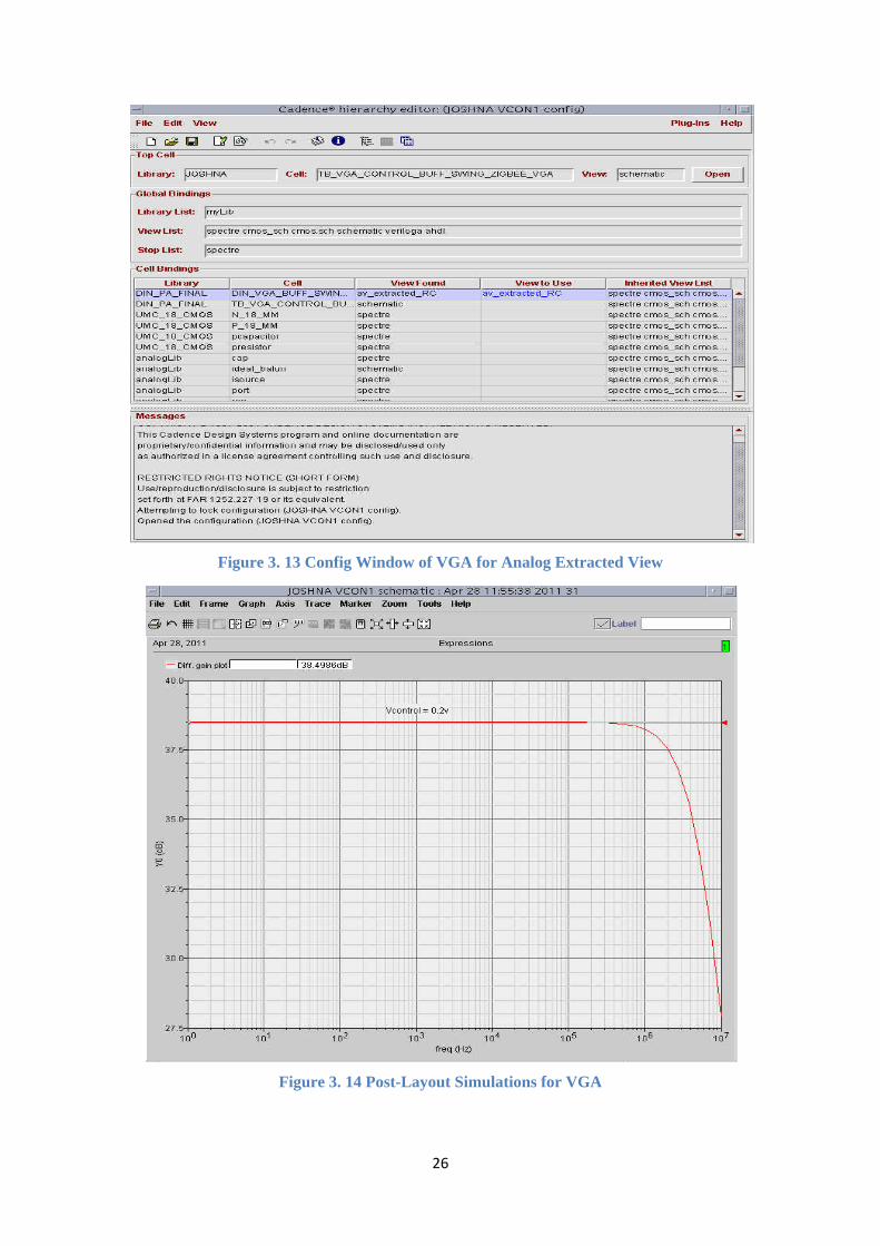
we generate a config window as shown in the Figure 3.13 and do the post layout simulation
same as like schematic simulation.
26
Figure 3. 13 Config Window of VGA for Analog Extracted View
Figure 3. 14 Post-Layout Simulations for VGA

27
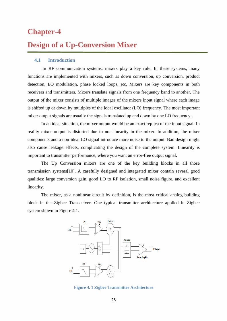
The Post layout simulation for VGA as shown in the Figure 3.14 differs slightly from
schematic simulation due to the influence of circuit parasitics such as parasitic capacitances
and resistances.
28
Chapter-4
Design of a Up-Conversion Mixer
4.1 Introduction
In RF communication systems, mixers play a key role. In these systems, many
functions are implemented with mixers, such as down conversion, up conversion, product
detection, I/Q modulation, phase locked loops, etc. Mixers are key components in both
receivers and transmitters. Mixers translate signals from one frequency band to another. The
output of the mixer consists of multiple images of the mixers input signal where each image
is shifted up or down by multiples of the local oscillator (LO) frequency. The most important
mixer output signals are usually the signals translated up and down by one LO frequency.
In an ideal situation, the mixer output would be an exact replica of the input signal. In
reality mixer output is distorted due to non-linearity in the mixer. In addition, the mixer
components and a non-ideal LO signal introduce more noise to the output. Bad design might
also cause leakage effects, complicating the design of the complete system. Linearity is
important to transmitter performance, where you want an error-free output signal.
The Up Conversion mixers are one of the key building blocks in all those
transmission systems[10]. A carefully designed and integrated mixer contain several good
qualities: large conversion gain, good LO to RF isolation, small noise figure, and excellent
linearity.
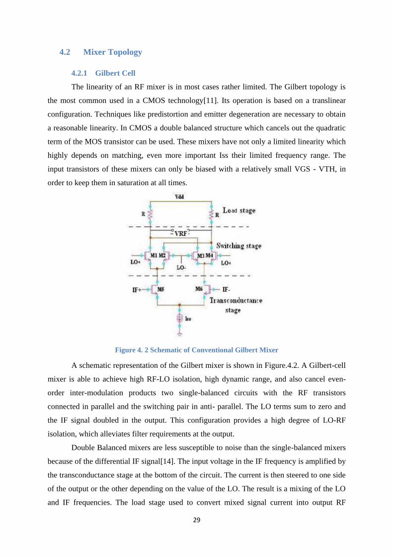
The mixer, as a nonlinear circuit by definition, is the most critical analog building
block in the Zigbee Transceiver. One typical transmitter architecture applied in Zigbee
system shown in Figure 4.1.
Figure 4. 1 Zigbee Transmitter Architecture
29
4.2 Mixer Topology
4.2.1 Gilbert Cell
The linearity of an RF mixer is in most cases rather limited. The Gilbert topology is
the most common used in a CMOS technology[11]. Its operation is based on a translinear
configuration. Techniques like predistortion and emitter degeneration are necessary to obtain
a reasonable linearity. In CMOS a double balanced structure which cancels out the quadratic
term of the MOS transistor can be used. These mixers have not only a limited linearity which
highly depends on matching, even more important Iss their limited frequency range. The
input transistors of these mixers can only be biased with a relatively small VGS - VTH, in
order to keep them in saturation at all times.
Figure 4. 2 Schematic of Conventional Gilbert Mixer
A schematic representation of the Gilbert mixer is shown in Figure.4.2. A Gilbert-cell
mixer is able to achieve high RF-LO isolation, high dynamic range, and also cancel even-
order inter-modulation products two single-balanced circuits with the RF transistors
connected in parallel and the switching pair in anti- parallel. The LO terms sum to zero and
the IF signal doubled in the output. This configuration provides a high degree of LO-RF
isolation, which alleviates filter requirements at the output.
Double Balanced mixers are less susceptible to noise than the single-balanced mixers
because of the differential IF signal[14]. The input voltage in the IF frequency is amplified by
the transconductance stage at the bottom of the circuit. The current is then steered to one side
of the output or the other depending on the value of the LO. The result is a mixing of the LO
and IF frequencies. The load stage used to convert mixed signal current into output RF

30
voltage, these resistors will influence the overall gain of the system and will be limited by
remaining headroom voltage[15].
It is often that two factors affect linearity in the mixer circuit. First, if the applied
signal at the driver stage is greater than the maximum differential input (also known as
overdriving), the first compression will take place. Linearity can be improved in this situation
by decreasing the driver stage transistor ratio (W/L), or increasing the bias current. The
second, once the output load resistor size R is too large, the voltage drop VDS across the
switching transistors will decrease, forcing the switching transistors out of saturation and into
the triode region of operation (VDS ≤ VGS – VTH).Reducing the size of the load resistors
force the DC output voltage to a higher level, which make the gain lower.
However, three stacked transistors imply quite high supply voltage in the order of
above 1.8 V and a strong LO voltage. This is a serious drawback of this architecture with
respect to power consumption. But a reduction of the supply voltage leads to worse
conversion gain and linearity performance.
Besides, the Gilbert mixer is based on the square-law characteristic of the MOS
transistor in saturation. This characteristic restricts the linear range of the multiplier to small
input voltage. The Gilbert cell has to be modified in order to cancel the quadratic terms
originating from the basic MOS device for improving linearity and support low voltage
operation[16]. Since in the conventional Gilbert Cell mixer, the IF input transistors operate in
the saturation region and the LO transistors operate in the perfect switching situation.
Consequently, it appears that the mixer performance in terms of conversion gain and
linearity can be simply improved by increasing the bias current of the driver stage. The IIP3
determines the maximum signal level that the mixer can handle a mixer with low NF and
high IIP3 has larger dynamic range.
4.3 Performance Parameters
4.3.1 Conversion Gain
The conversion gain of a mixer is defined as the ratio of the desired IF output to the RF input.
If the ratio is less than 1, it is referred as a conversion loss. Conversion gain is expressed in
terms of voltage or power and it is usually given in dB:
Power Gain (dB) = 10 log
31
Voltage Gain (dB) = 20 log
If input is matched, the relationship between power gain and voltage gain is given by:
Power Gain (dB) = Voltage Gain (dB) +10 log
where RS is the source resistance and RL is the load resistance.
The conversion gain of a mixer is important because it affects the noise figure and linearity of
the overall s by the loss. Moreover, the conversion gain of the mixer also determines the
signal level at the output of the mixer, in which the signal will be fed into the following
stages. Therefore, the conversion gain will affect the linearity performance of the system.
4.3.2 Gain Compression
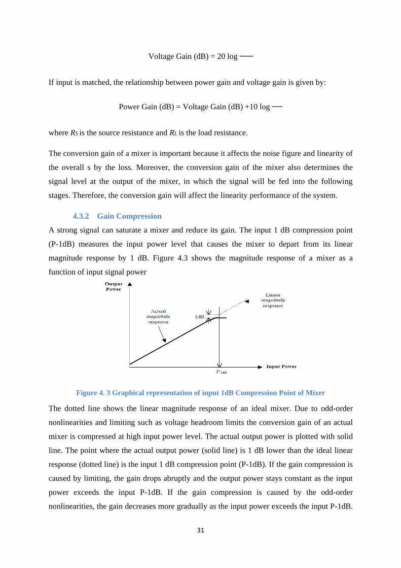
A strong signal can saturate a mixer and reduce its gain. The input 1 dB compression point
(P-1dB) measures the input power level that causes the mixer to depart from its linear
magnitude response by 1 dB. Figure 4.3 shows the magnitude response of a mixer as a
function of input signal power
Figure 4. 3 Graphical representation of input 1dB Compression Point of Mixer
The dotted line shows the linear magnitude response of an ideal mixer. Due to odd-order
nonlinearities and limiting such as voltage headroom limits the conversion gain of an actual
mixer is compressed at high input power level. The actual output power is plotted with solid
line. The point where the actual output power (solid line) is 1 dB lower than the ideal linear
response (dotted line) is the input 1 dB compression point (P-1dB). If the gain compression is
caused by limiting, the gain drops abruptly and the output power stays constant as the input
power exceeds the input P-1dB. If the gain compression is caused by the odd-order
nonlinearities, the gain decreases more gradually as the input power exceeds the input P-1dB.
32
At medium input power levels, gain compression is dominated by the third-order
nonlinearity. If the input power continues to increase, higher-order non-linearities become
significant.
4.3.3 Third order Intermodulation Distortion
The major function of a mixer is to perform frequency translation. Therefore it is inherently a
non-linear circuit. However it is desirable for a mixer to behave very linearly with respect to
all non-linearities except the one giving the desired frequency conversion. If we apply two
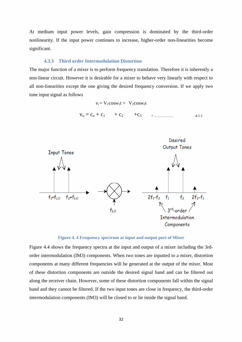
tone input signal as follows
vi = V1cosw1t + V2cosw2t
vo = co + c1 + c2 +c3 + ……………. 4.1.1
Figure 4. 4 Frequency spectrum at input and output port of Mixer
Figure 4.4 shows the frequency spectra at the input and output of a mixer including the 3rd-
order intermodulation (IM3) components. When two tones are inputted to a mixer, distortion
components at many different frequencies will be generated at the output of the mixer. Most
of these distortion components are outside the desired signal band and can be filtered out
along the receiver chain. However, some of these distortion components fall within the signal
band and they cannot be filtered. If the two input tones are close in frequency, the third-order
intermodulation components (IM3) will be closed to or lie inside the signal band.
33
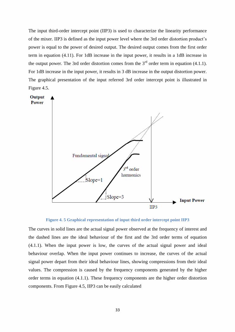
The input third-order intercept point (IIP3) is used to characterize the linearity performance
of the mixer. IIP3 is defined as the input power level where the 3rd order distortion product’s
power is equal to the power of desired output. The desired output comes from the first order
term in equation (4.11). For 1dB increase in the input power, it results in a 1dB increase in
the output power. The 3rd order distortion comes from the 3rd
order term in equation (4.1.1).
For 1dB increase in the input power, it results in 3 dB increase in the output distortion power.
The graphical presentation of the input referred 3rd order intercept point is illustrated in
Figure 4.5.
Figure 4. 5 Graphical representation of input third order intercept point IIP3
The curves in solid lines are the actual signal power observed at the frequency of interest and
the dashed lines are the ideal behaviour of the first and the 3rd order terms of equation
(4.1.1). When the input power is low, the curves of the actual signal power and ideal
behaviour overlap. When the input power continues to increase, the curves of the actual
signal power depart from their ideal behaviour lines, showing compressions from their ideal
values. The compression is caused by the frequency components generated by the higher
order terms in equation (4.1.1). These frequency components are the higher order distortion
components. From Figure 4.5, IIP3 can be easily calculated
34
IIP3 = +
where Pout1 and Pout3 are the measured output power of the desired signal and the 3rd order
distortion respectively and Pin is the input power.
4.4 Proposed up conversion mixer for High Linearity
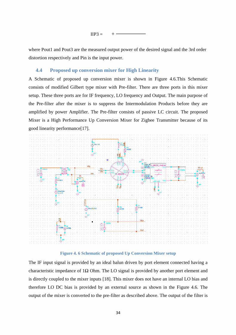
A Schematic of proposed up conversion mixer is shown in Figure 4.6.This Schematic
consists of modified Gilbert type mixer with Pre-filter. There are three ports in this mixer
setup. These three ports are for IF frequency, LO frequency and Output. The main purpose of
the Pre-filter after the mixer is to suppress the Intermodulation Products before they are
amplified by power Amplifier. The Pre-filter consists of passive LC circuit. The proposed
Mixer is a High Performance Up Conversion Mixer for Zigbee Transmitter because of its
good linearity performance[17].
Figure 4. 6 Schematic of proposed Up Conversion Mixer setup
The IF input signal is provided by an ideal balun driven by port element connected having a
characteristic impedance of 1Ω Ohm. The LO signal is provided by another port element and
is directly coupled to the mixer inputs [18]. This mixer does not have an internal LO bias and
therefore LO DC bias is provided by an external source as shown in the Figure 4.6. The
output of the mixer is converted to the pre-filter as described above. The output of the filter is
35
connected to a port element having 50Ω Ohm characteristic impedance. The output is also
converted to a single-ended output by a vcvs (Voltage-Controlled Voltage Source) element.
The mixer is characterized at the block level. Therefore, it is important to include other
circuit elements to represent parasitic associated with the top-level chip, package, and printed
circuit board (PCB) substrate interconnect. If models for these interconnect elements are not
available then estimated models can be implemented using lumped elements as is done here.
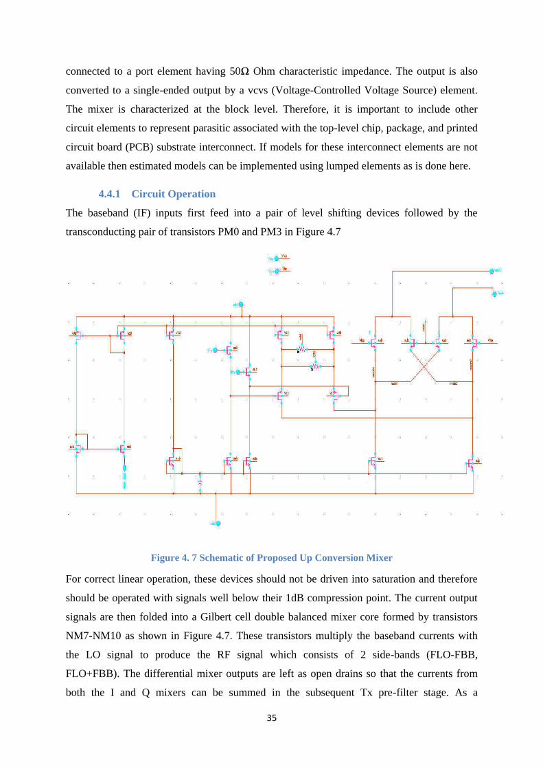
4.4.1 Circuit Operation
The baseband (IF) inputs first feed into a pair of level shifting devices followed by the
transconducting pair of transistors PM0 and PM3 in Figure 4.7
Figure 4. 7 Schematic of Proposed Up Conversion Mixer
For correct linear operation, these devices should not be driven into saturation and therefore
should be operated with signals well below their 1dB compression point. The current output
signals are then folded into a Gilbert cell double balanced mixer core formed by transistors
NM7-NM10 as shown in Figure 4.7. These transistors multiply the baseband currents with
the LO signal to produce the RF signal which consists of 2 side-bands (FLO-FBB,
FLO+FBB). The differential mixer outputs are left as open drains so that the currents from
both the I and Q mixers can be summed in the subsequent Tx pre-filter stage. As a
36
consequence of the quadrature LO drive and the summation process the upper sideband RF
products will add constructively while the lower sideband products are suppressed
Figure 4. 8 Schematic of Pre-filter
The pre-filter shown in Figure 4.8 consists of a passive LC-circuit. In addition to being the
output load for both mixers forming the I/Q modulator it helps to suppress the higher order
modulation products before they are amplified by the power amplifier [19].
4.5 Results and Discussion
The mixer circuit is simulated in Cadence© using SpectreRF simulator in UMC-0.18um
Mixed Signal CMOS RF models. The mixer is designed to operate at 1.8V voltage supply.
Frequencies of three ports in the mixer are specified at IF Frequency of 5 MHz, LO
frequency of 2.45 GHz and RF frequency of 2.45GHz respectively.
A mixer’s frequency conversion is characterized by conversion gain. The voltage conversion
gain is the ratio of the RMS voltages of the RF and IF signals. The conversion gain is
measured to be –11.3dB.Choosen PAC and PSS analysis for simulating Conversion Gain and
IIP3.
37
Figure 4. 9 Analog Design Environment for Conversion Gain
Figure 4. 10 Conversion Gain of the Proposed Mixer
The linearity performance is measured using two-tone test. A second input signal is input to
the RF ports of the mixer. The RF signal frequency is at 1.9GHz, and the second input signal
frequency is at 1.901GHz. IIP3 is the extrapolated intercept point between fundamental term
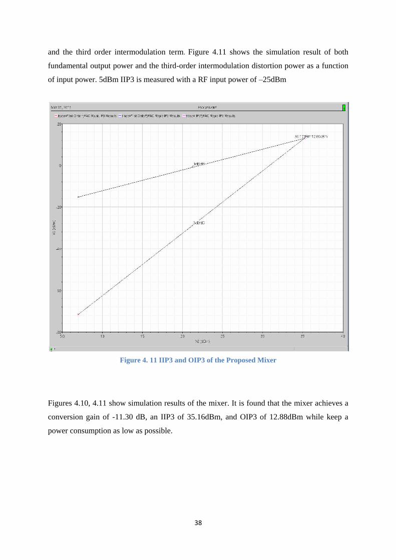
38
and the third order intermodulation term. Figure 4.11 shows the simulation result of both
fundamental output power and the third-order intermodulation distortion power as a function
of input power. 5dBm IIP3 is measured with a RF input power of –25dBm
Figure 4. 11 IIP3 and OIP3 of the Proposed Mixer
Figures 4.10, 4.11 show simulation results of the mixer. It is found that the mixer achieves a
conversion gain of -11.30 dB, an IIP3 of 35.16dBm, and OIP3 of 12.88dBm while keep a
power consumption as low as possible.
39
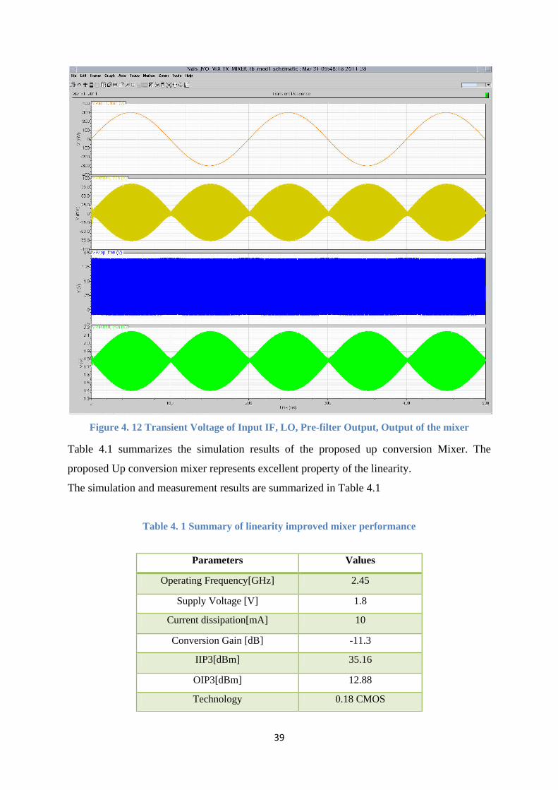
Figure 4. 12 Transient Voltage of Input IF, LO, Pre-filter Output, Output of the mixer
Table 4.1 summarizes the simulation results of the proposed up conversion Mixer. The
proposed Up conversion mixer represents excellent property of the linearity.
The simulation and measurement results are summarized in Table 4.1
Table 4. 1 Summary of linearity improved mixer performance
Parameters Values
Operating Frequency[GHz] 2.45
Supply Voltage [V] 1.8
Current dissipation[mA] 10
Conversion Gain [dB] -11.3
IIP3[dBm] 35.16
OIP3[dBm] 12.88
Technology 0.18 CMOS
40
Chapter-5
Design of a Power Amplifier
5.1 Introduction
Power Amplifiers (PAs) are key components in the wireless communications industry,
TV transmissions, Radar, and RF heating which consume a great amount of power in overall
transceiver. The PAs must achieve high operation efficiency in order to maximize the battery
life and minimize the size and cost. The general PA design focuses on the whole system
architecture and should achieve advantages in terms of performance, cost, and size. To allow
full system integration and low costs, CMOS technology is well suited. To achieve a high
linearity, class-A power amplifiers are preferred.
Many efforts have been made on RF block integration using CMOS technology. But, it
is still a big challenge for CMOS PA to be competitive with the PAs made of compound
semi-conductor, the power amplifier is regarded as the last key area to be solved for the
single chip solution. There are two main issues in the design of PAs in CMOS process,
namely, gate oxide breakdown and hot carrier effects, which restrict the output power.
Moreover, both problems get worse as the technology scales. For the PA based WLAN
standards, the linearity is a key parameter which is closely related to the power consumption
and distortion.
In an implantable system, the power consumption needs to be reduced to the minimum
possible limit such that the battery needs not be charged repeatedly. Since the power
amplifier is the unit that consumes most of the transmitter’s power an efficient PA is needed
to achieve the required level of low power consumption. The Modulation scheme used in
ZigBee is OQPSK modulation. It is a variant of QPSK modulation formed by staggering the
inphase and quadrature components of QPSK by half a symbol period thus the maximum
allowed phase shift is 90°. When OQPSK is band limited, the resulting intersymbol
interference (ISI) will cause the envelope to droop slightly in the region of a ±90° transition
instead of being constant envelope .This will increase spectral regrowth and out of band
emission. To avoid these problems linear classes of PA, Class A Power Amplifier had been
used with ZigBee transmitters
41
5.2 RF Power Amplifier Classification
Class of amplifier operation differ not in only the method of operation and efficiency,
but also in their power-output capability. The power-output capability is defined as output
power per transistor normalized for peak drain voltage and current of 1V and 1A,
respectively. In general, RF power Amplifier can be defined by two: Linear amplifier and
nonlinear amplifier. Linear amplifiers attempt to preserve the original wave shape of the input
signal into the output signal. The main classes of linear amplifier are: Class A, Class B,Class
AB.
Nonlinear amplifier can’t attempt to preserve the original wave shape of the input
signal at the output, but it can perform a better power efficiency. The main classes of
nonlinear amplifier are: Class C, Class E, Class F and some other Class G, Class H, and Class
S.
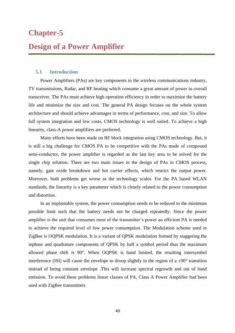
5.2.1 Class A Power Amplifier
Class A amplifier is the simplest power amplifier type in terms of design and
construction. The Class A amplifier has a conduction angle of 360°. Conduction angle refers
to the time period for which a device is conducting. Thus a conduction angle of 360° tell us
that in Class A operation the device conducts current for the entire input cycle. Class A
amplifier are considered to be the most linear since the transistor is biased in the centre of the
load line to allow for maximum voltage and current swings without cut-off saturation
(a) (b)
Figure 5. 1 (a) Class A Power Amplifier, (b) Biasing for Class A Power Amplifier
Radio Frequency Choke represents a large inductor which makes the supply voltage to be
lowered by a factor of two because VX can swing from approximately 0 to 2VDD.
42
How, the quiescent current is large enough that the transistor remains at all times in the active
region and acts as a current source, controlled by the drive. As a result, it can be shown that
the maximum efficiency achievable from a Class A power amplifier is only 50%. And this is
a theoretical number and the actual efficiency is typically much less.
The maximum ac output voltage Vom is slightly less than VDD and the maximum ac
output current Iom is equal to Idq in Class A amplifier. In the inductor-less system, the output
voltage Vom will not be able to rise above the supply voltage, therefore, the swing will be
constrained to VDD/2 and not VDD. The drain voltage must have a dc component equal to
that of the supply voltage and a fundamental-frequency component equal to that of the output
voltage; hence
VD = VDD + Vom sinθ
The dc Power Pdc= VDD .Idq
The maximum output power is
Po = Vom Iom VDD .Idq
And the efficiency is
.100 = .100 ≤ 50 %
The difference between the dc power and output power is called power dissipation
Pd= Pdc - Po
5.2.2 Class B Power Amplifier
This is an amplifier in which the conduction angle for the transistor is approximately
180°.The gate bias in class B is set at the threshold voltage point of the transistor. Hence
there is a current flowing at the output of the device only when there is a signal at the input.
Mover the device would conduct current only when the input signal level is greater than the
threshold voltage.
The class-B amplifier operates ideally at zero quiescent current, so that the dc power
is small. Therefore, its efficiency is higher than that of the class-A amplifier. The price paid
for the enhancement in the efficiency is in the linearity of the device.
Common configuration of Class-B amplifier is push-pull amplifier as shown in Figure
5.2. In this configuration one transistor conducts during positive half cycles of the input
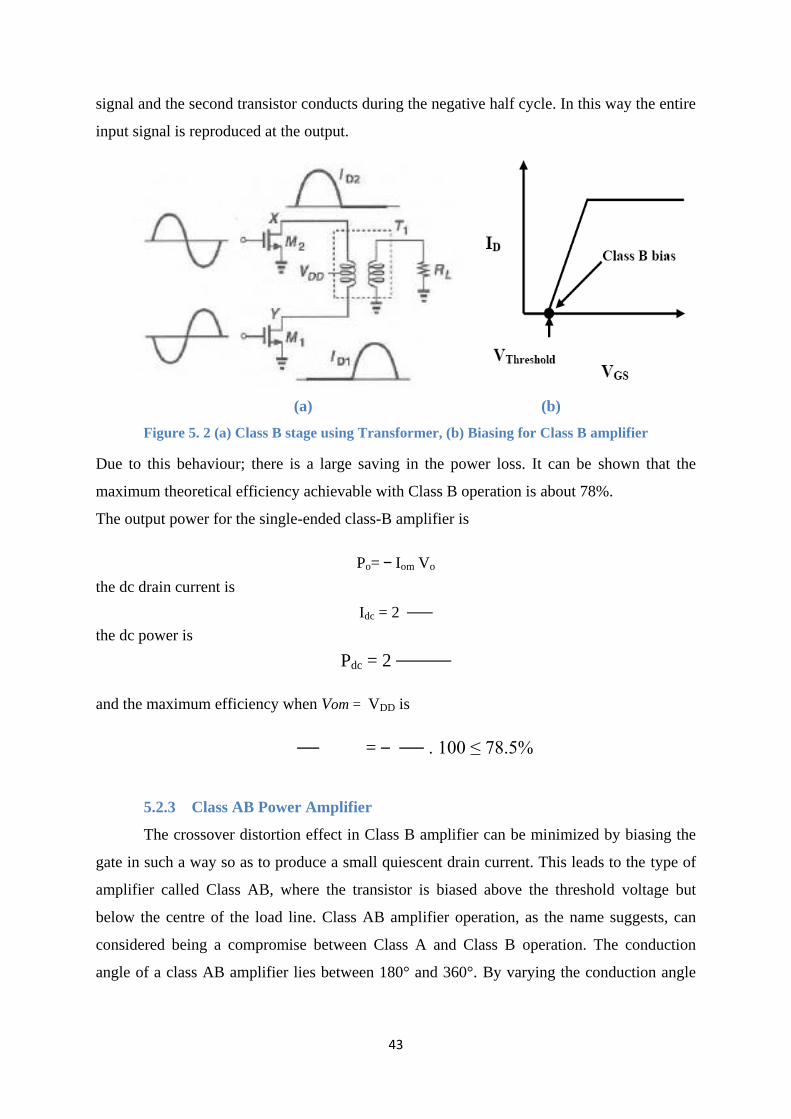
43
signal and the second transistor conducts during the negative half cycle. In this way the entire
input signal is reproduced at the output.
(a) (b)
Figure 5. 2 (a) Class B stage using Transformer, (b) Biasing for Class B amplifier
Due to this behaviour; there is a large saving in the power loss. It can be shown that the
maximum theoretical efficiency achievable with Class B operation is about 78%.
The output power for the single-ended class-B amplifier is
Po= Iom Vo
the dc drain current is
Idc = 2 the dc power is
Pdc = 2
and the maximum efficiency when Vom = VDD is
= . 100 ≤ 78.5%
5.2.3 Class AB Power Amplifier
The crossover distortion effect in Class B amplifier can be minimized by biasing the
gate in such a way so as to produce a small quiescent drain current. This leads to the type of
amplifier called Class AB, where the transistor is biased above the threshold voltage but
below the centre of the load line. Class AB amplifier operation, as the name suggests, can
considered being a compromise between Class A and Class B operation. The conduction
angle of a class AB amplifier lies between 180° and 360°. By varying the conduction angle
44
the amplifier can be made to behave more as a Class A or Class B amplifier; hence the
theoretical maximum efficiency of a Class AB amplifier 50° and 78.5°.
Figure 5. 3 Biasing for Class AB amplifier
But commercial Class AB amplifiers typically much lower efficiency in the order of
40-55%. Thus a trade-off between linearity and efficiency can be achieved by simply
changing the gate bias. Class AB amplifier can also be realized in push-pull configurations
even though single transistor configuration is preferred for high frequency linear operation.
5.2.4 Class C Power Amplifier
A Class C power amplifier is a non-linear power amplifier used in places where
linearity is not a requirement and high efficiency is highly desired. Class C amplifiers are
widely used in constant envelope modulation systems where linearity is not required. The
transistor is biased below threshold for Class C operation and hence the device conduction
angle varies from 0° and 180°.
(a) (b)
Figure 5. 4 (a) Class C stage , (b) Biasing for Class C amplifier
45
As shown in Figure 5.4 (a), the circuit is biased Such that M1 turns on if Vin = | Vb| +
VTH , where Vb is the negative voltage. In the other words the transistor stimulates the output
with a narrow current waveform in each cycle. The matching circuit usually includes some
filtering to suppress the harmonics.
The distinction between Class C and one transistor Class B stages is in conduction
angle θ. As θ decreases, the transistor on for a small fraction of the period, thus dissipating
less power. For the same reason, however the power delivered to the load also decreases. If
the current drawn by the transistor is assumed to be a piece of sinusoid and output voltage is a
sinusoid with a peak voltage equals to VDD, then the efficiency can be calculated as a function
of θ .The Efficiency is given by
η =
varying from 50% for θ = 360o (class A) to 79% for θ = 180
o (class B) to 100% for θ= 0
(class C).
The maximum efficiency of 100% is often considered as a prominent feature of class
C stages. However another attribute that must also be taken into account is the actual power
delivered to the load. The output Power is given as
Pout
This quantity drops to zero as the conduction angle vanishes. In other word Class C exhibits a
high efficiency only if it delivers a fraction of peak output power. For this reason, true Class
C is not suited to the transceivers, where efficiency at full output power is of greatest
concern.
5.2.5 Class D Power Amplifier
The voltage mode Class D amplifier is defined as a switching circuit that results in the
generation of a half-sinusoidal current waveform and a square voltage waveform. Class-D
PAs as shown in Figure 5.5(a) use two or more transistors as switches to generate a square
drain-voltage waveform. A series-tuned output filter passes only the fundamental-frequency
component to the load, Class-D amplifiers suffer from a number of problems that make them
difficult to realize, especially at high frequencies. First, the availability of suitable devices for
the upper switch is limited. Secondly, device parasitics such as drain-source capacitance and
46
lead inductance result in losses in each cycle. If realized, (they are common at low RF and
audio frequencies).
(a) (b)
Figure 5. 5 (a) Class D stage, (b) Class D voltage and Current Waveforms
Class-D amplifiers theoretically can reach 100% efficiency, as there is no period during a
cycle where the voltage and current waveforms overlap (current is drawn only through the
transistor that is on)as shown in Figure 5.5(b) .
5.2.6 Class E Power Amplifier
Class E power amplifiers are fundamentally different from the other types of power
amplifiers discussed before. In the previously described power amplifier classes, it was seen
that the operational differences were obtained by the selection of the bias point. However, in
a Class E amplifier as shown in Figure 5.6 (a), only circuit-independent signal guidelines are
given, and the topology is not as restricted.
(a) (b)
Figure 5. 6 (a) Class E stage , (b) Class E voltage and Current Waveforms
The idea behind the Class E amplifier is to have non-overlapping output voltage and
output current waveforms as shown in Figure 5.6 (b), and to limit the values of the voltage,
current, and the derivative of the voltage with respect to time at the instants when the
transition between non-zero currents and non-zero voltage occurs.
47
For Class E amplifier operation, the transistor acts like a switch. Also the terms “on”
state and “off” state are used to describe the time period when the transistor starts conducting
and stops conducting respectively. The voltage across the switch must return to zero just
before the switch turns “on” and starts conducting current. Similarly the current through the
switch must return to zero just before the switch turns “off”. These two conditions avoid the
energy dissipation caused by the simultaneous superposition of substantial voltage and
current on the switching transistor during transition from “on” to “off” state or “off” to “on”
state. Another condition for Class E operation is that the voltage across the switch must return
to zero with zero slope (i.e., di/dt = 0) and the voltage across the transistor at the beginning of
“on” state is zero. Hence for deviation in the switching instant from the ideal switching time
the corresponding output voltage or current will be very small, and the power lost in the
device due to this non-ideal will be relatively small. With all these conditions satisfied, very
high efficiencies can be achieved. The maximum theoretical efficiency of Class E amplifier is
100%.
5.2.7 Class F Power Amplifier
Class-F power amplifiers are usually considered as very high efficiency (80% or more
Power-Added Efficiency) amplifiers where the high efficiency is obtained through the use of
harmonic traps (L-C filters or quarter-wavelength transmission lines) which provide suitable
terminations (either open or short) for the harmonics generated.
(a) (b)
Figure 5. 7 (a) Class F stage , (b) Class F voltage and Current Waveforms
By doing this, square wave drain voltage and a peaked half-sinusoidal drain current out of
phase by 180% are produced. Since only a drain voltage or a drain current exists at any given
time, the power dissipation is ideally zero resulting in 100% theoretical efficiency. These
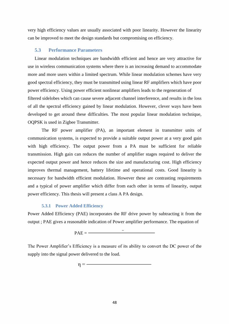
48
very high efficiency values are usually associated with poor linearity. However the linearity
can be improved to meet the design standards but compromising on efficiency.
5.3 Performance Parameters
Linear modulation techniques are bandwidth efficient and hence are very attractive for
use in wireless communication systems where there is an increasing demand to accommodate
more and more users within a limited spectrum. While linear modulation schemes have very
good spectral efficiency, they must be transmitted using linear RF amplifiers which have poor
power efficiency. Using power efficient nonlinear amplifiers leads to the regeneration of
filtered sidelobes which can cause severe adjacent channel interference, and results in the loss
of all the spectral efficiency gained by linear modulation. However, clever ways have been
developed to get around these difficulties. The most popular linear modulation technique,
OQPSK is used in Zigbee Transmitter.
The RF power amplifier (PA), an important element in transmitter units of
communication systems, is expected to provide a suitable output power at a very good gain
with high efficiency. The output power from a PA must be sufficient for reliable
transmission. High gain can reduces the number of amplifier stages required to deliver the
expected output power and hence reduces the size and manufacturing cost. High efficiency
improves thermal management, battery lifetime and operational costs. Good linearity is
necessary for bandwidth efficient modulation. However these are contrasting requirements
and a typical of power amplifier which differ from each other in terms of linearity, output
power efficiency. This thesis will present a class A PA design.
5.3.1 Power Added Efficiency
Power Added Efficiency (PAE) incorporates the RF drive power by subtracting it from the
output ; PAE gives a reasonable indication of Power amplifier performance. The equation of
PAE = –
The Power Amplifier’s Efficiency is a measure of its ability to convert the DC power of the
supply into the signal power delivered to the load.
η =
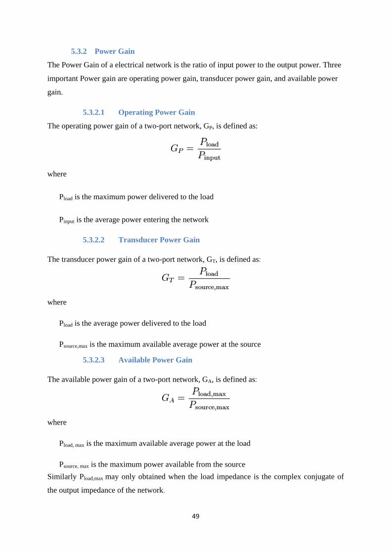
49
5.3.2 Power Gain
The Power Gain of a electrical network is the ratio of input power to the output power. Three
important Power gain are operating power gain, transducer power gain, and available power
gain.
5.3.2.1 Operating Power Gain
The operating power gain of a two-port network, GP, is defined as:
where
Pload is the maximum power delivered to the load
Pinput is the average power entering the network
5.3.2.2 Transducer Power Gain
The transducer power gain of a two-port network, GT, is defined as:
where
Pload is the average power delivered to the load
Psource,max is the maximum available average power at the source
5.3.2.3 Available Power Gain
The available power gain of a two-port network, GA, is defined as:
where
Pload, max is the maximum available average power at the load
Psource, max is the maximum power available from the source
Similarly Pload,max may only obtained when the load impedance is the complex conjugate of
the output impedance of the network.
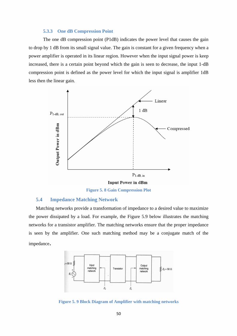
50
5.3.3 One dB Compression Point
The one dB compression point (P1dB) indicates the power level that causes the gain
to drop by 1 dB from its small signal value. The gain is constant for a given frequency when a
power amplifier is operated in its linear region. However when the input signal power is keep
increased, there is a certain point beyond which the gain is seen to decrease, the input 1-dB
compression point is defined as the power level for which the input signal is amplifier 1dB
less then the linear gain.
Figure 5. 8 Gain Compression Plot
5.4 Impedance Matching Network
Matching networks provide a transformation of impedance to a desired value to maximize
the power dissipated by a load. For example, the Figure 5.9 below illustrates the matching
networks for a transistor amplifier. The matching networks ensure that the proper impedance
is seen by the amplifier. One such matching method may be a conjugate match of the
impedance.
Figure 5. 9 Block Diagram of Amplifier with matching networks
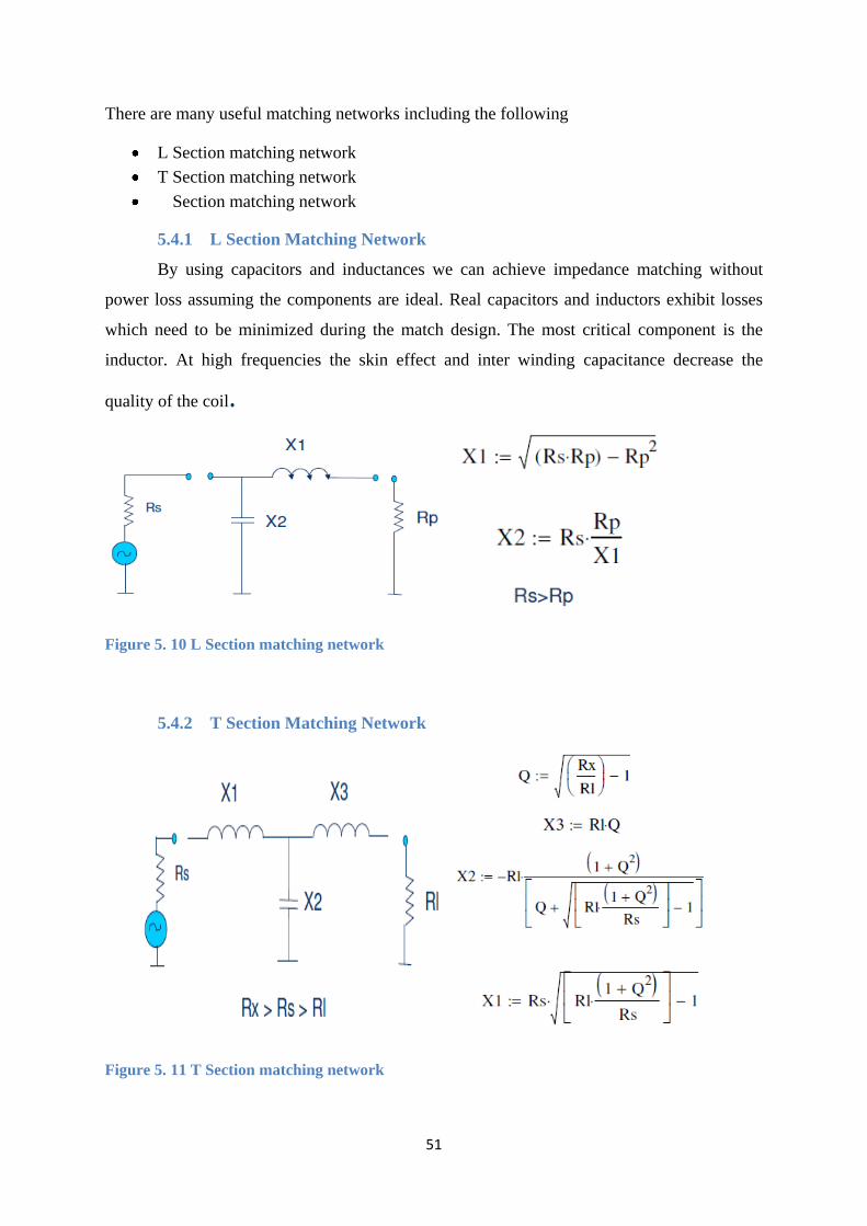
51
There are many useful matching networks including the following
L Section matching network
T Section matching network
Section matching network
5.4.1 L Section Matching Network
By using capacitors and inductances we can achieve impedance matching without
power loss assuming the components are ideal. Real capacitors and inductors exhibit losses
which need to be minimized during the match design. The most critical component is the
inductor. At high frequencies the skin effect and inter winding capacitance decrease the
quality of the coil.
Figure 5. 10 L Section matching network
5.4.2 T Section Matching Network
Figure 5. 11 T Section matching network
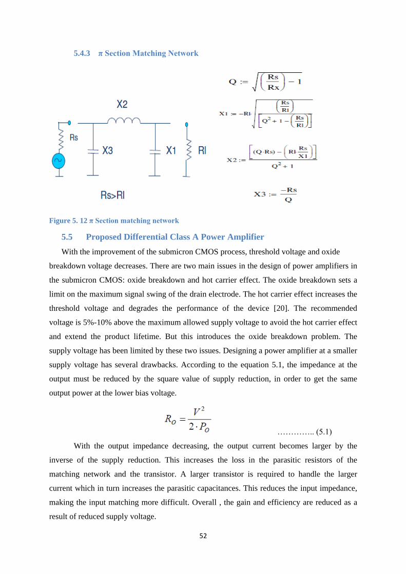
52
5.4.3 π Section Matching Network
Figure 5. 12 π Section matching network
5.5 Proposed Differential Class A Power Amplifier
With the improvement of the submicron CMOS process, threshold voltage and oxide
breakdown voltage decreases. There are two main issues in the design of power amplifiers in
the submicron CMOS: oxide breakdown and hot carrier effect. The oxide breakdown sets a
limit on the maximum signal swing of the drain electrode. The hot carrier effect increases the
threshold voltage and degrades the performance of the device [20]. The recommended
voltage is 5%-10% above the maximum allowed supply voltage to avoid the hot carrier effect
and extend the product lifetime. But this introduces the oxide breakdown problem. The
supply voltage has been limited by these two issues. Designing a power amplifier at a smaller
supply voltage has several drawbacks. According to the equation 5.1, the impedance at the
output must be reduced by the square value of supply reduction, in order to get the same
output power at the lower bias voltage.
………….. (5.1)
With the output impedance decreasing, the output current becomes larger by the
inverse of the supply reduction. This increases the loss in the parasitic resistors of the
matching network and the transistor. A larger transistor is required to handle the larger
current which in turn increases the parasitic capacitances. This reduces the input impedance,
making the input matching more difficult. Overall , the gain and efficiency are reduced as a
result of reduced supply voltage.
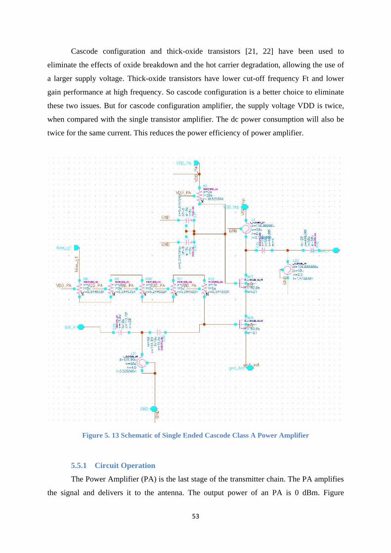
53
Cascode configuration and thick-oxide transistors [21, 22] have been used to
eliminate the effects of oxide breakdown and the hot carrier degradation, allowing the use of
a larger supply voltage. Thick-oxide transistors have lower cut-off frequency Ft and lower
gain performance at high frequency. So cascode configuration is a better choice to eliminate
these two issues. But for cascode configuration amplifier, the supply voltage VDD is twice,
when compared with the single transistor amplifier. The dc power consumption will also be
twice for the same current. This reduces the power efficiency of power amplifier.
Figure 5. 13 Schematic of Single Ended Cascode Class A Power Amplifier
5.5.1 Circuit Operation
The Power Amplifier (PA) is the last stage of the transmitter chain. The PA amplifies
the signal and delivers it to the antenna. The output power of an PA is 0 dBm. Figure
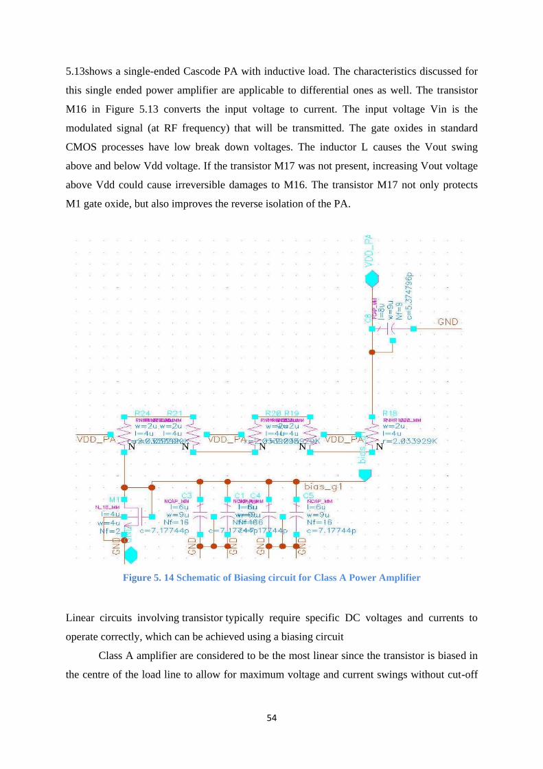
54
5.13shows a single-ended Cascode PA with inductive load. The characteristics discussed for
this single ended power amplifier are applicable to differential ones as well. The transistor
M16 in Figure 5.13 converts the input voltage to current. The input voltage Vin is the
modulated signal (at RF frequency) that will be transmitted. The gate oxides in standard
CMOS processes have low break down voltages. The inductor L causes the Vout swing
above and below Vdd voltage. If the transistor M17 was not present, increasing Vout voltage
above Vdd could cause irreversible damages to M16. The transistor M17 not only protects
M1 gate oxide, but also improves the reverse isolation of the PA.
Figure 5. 14 Schematic of Biasing circuit for Class A Power Amplifier
Linear circuits involving transistor typically require specific DC voltages and currents to
operate correctly, which can be achieved using a biasing circuit
Class A amplifier are considered to be the most linear since the transistor is biased in
the centre of the load line to allow for maximum voltage and current swings without cut-off
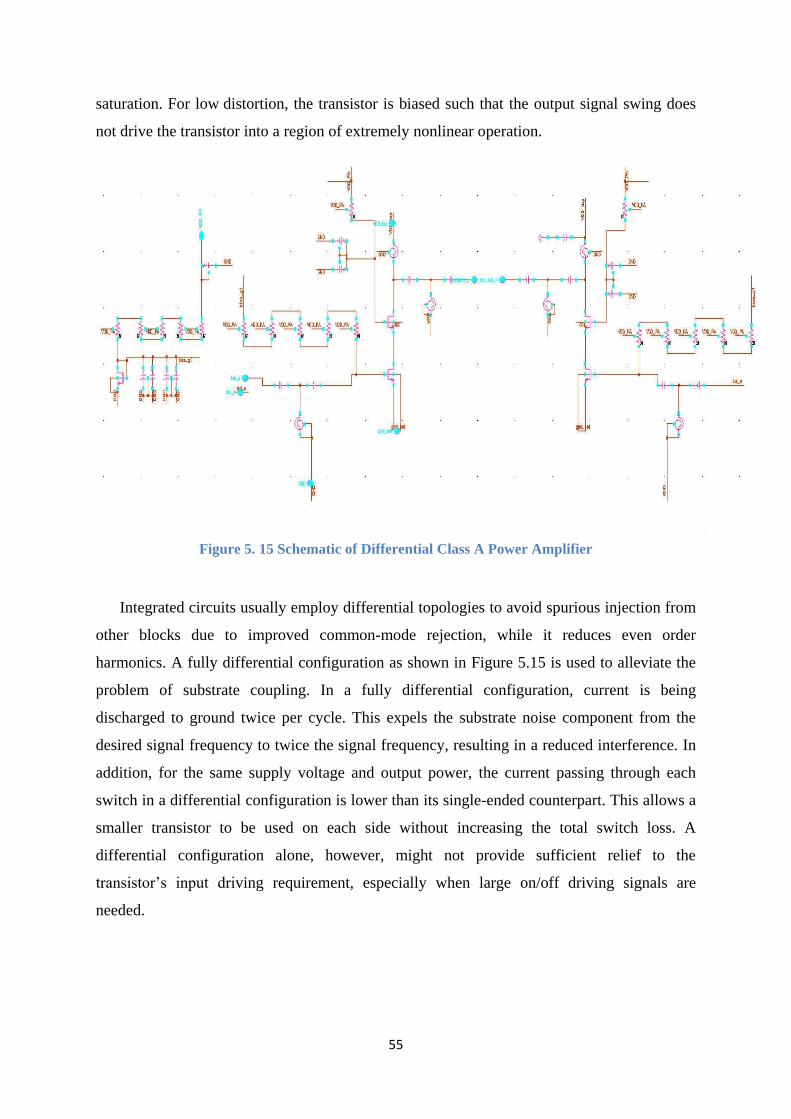
55
saturation. For low distortion, the transistor is biased such that the output signal swing does
not drive the transistor into a region of extremely nonlinear operation.
Figure 5. 15 Schematic of Differential Class A Power Amplifier
Integrated circuits usually employ differential topologies to avoid spurious injection from
other blocks due to improved common-mode rejection, while it reduces even order
harmonics. A fully differential configuration as shown in Figure 5.15 is used to alleviate the
problem of substrate coupling. In a fully differential configuration, current is being
discharged to ground twice per cycle. This expels the substrate noise component from the
desired signal frequency to twice the signal frequency, resulting in a reduced interference. In
addition, for the same supply voltage and output power, the current passing through each
switch in a differential configuration is lower than its single-ended counterpart. This allows a
smaller transistor to be used on each side without increasing the total switch loss. A
differential configuration alone, however, might not provide sufficient relief to the
transistor’s input driving requirement, especially when large on/off driving signals are
needed.
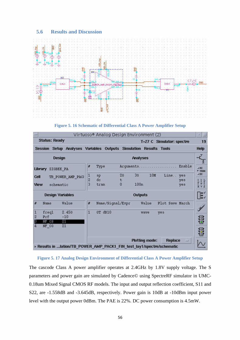
56
5.6 Results and Discussion
Figure 5. 16 Schematic of Differential Class A Power Amplifier Setup
Figure 5. 17 Analog Design Environment of Differential Class A Power Amplifier Setup
The cascode Class A power amplifier operates at 2.4GHz by 1.8V supply voltage. The S
parameters and power gain are simulated by Cadence© using SpectreRF simulator in UMC-
0.18um Mixed Signal CMOS RF models. The input and output reflection coefficient, S11 and
S22, are -1.558dB and -3.645dB, respectively. Power gain is 10dB at -10dBm input power
level with the output power 0dBm. The PAE is 22%. DC power consumption is 4.5mW.
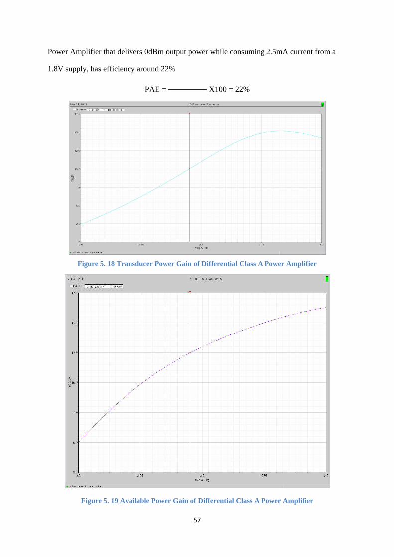
57
Power Amplifier that delivers 0dBm output power while consuming 2.5mA current from a
1.8V supply, has efficiency around 22%
PAE = X100 = 22%
Figure 5. 18 Transducer Power Gain of Differential Class A Power Amplifier
Figure 5. 19 Available Power Gain of Differential Class A Power Amplifier
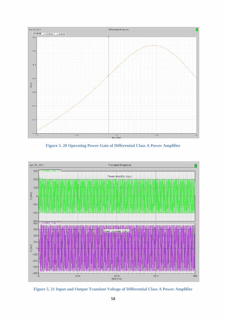
58
Figure 5. 20 Operating Power Gain of Differential Class A Power Amplifier
Figure 5. 21 Input and Output Transient Voltage of Differential Class A Power Amplifier
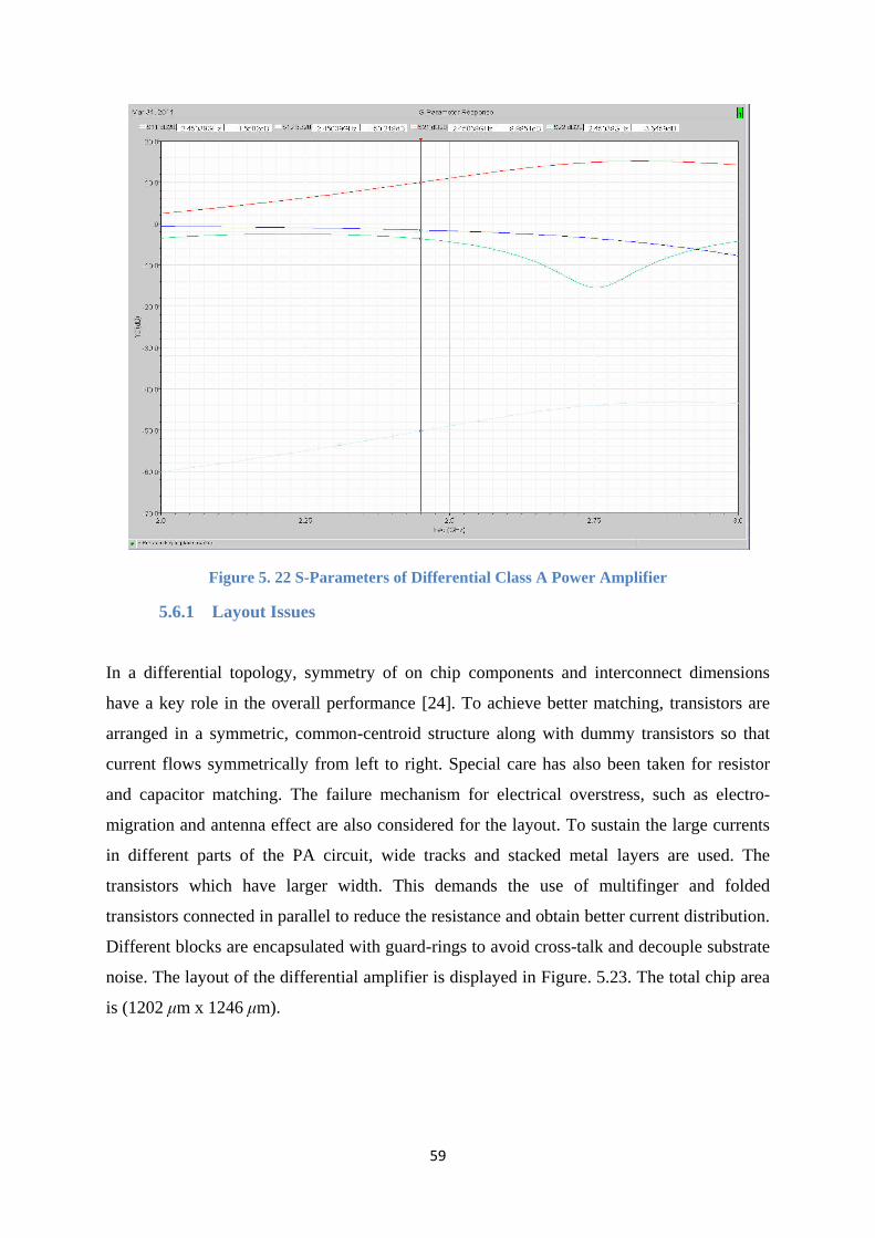
59
Figure 5. 22 S-Parameters of Differential Class A Power Amplifier
5.6.1 Layout Issues
In a differential topology, symmetry of on chip components and interconnect dimensions
have a key role in the overall performance [24]. To achieve better matching, transistors are
arranged in a symmetric, common-centroid structure along with dummy transistors so that
current flows symmetrically from left to right. Special care has also been taken for resistor
and capacitor matching. The failure mechanism for electrical overstress, such as electro-
migration and antenna effect are also considered for the layout. To sustain the large currents
in different parts of the PA circuit, wide tracks and stacked metal layers are used. The
transistors which have larger width. This demands the use of multifinger and folded
transistors connected in parallel to reduce the resistance and obtain better current distribution.
Different blocks are encapsulated with guard-rings to avoid cross-talk and decouple substrate
noise. The layout of the differential amplifier is displayed in Figure. 5.23. The total chip area
is (1202 μm x 1246 μm).
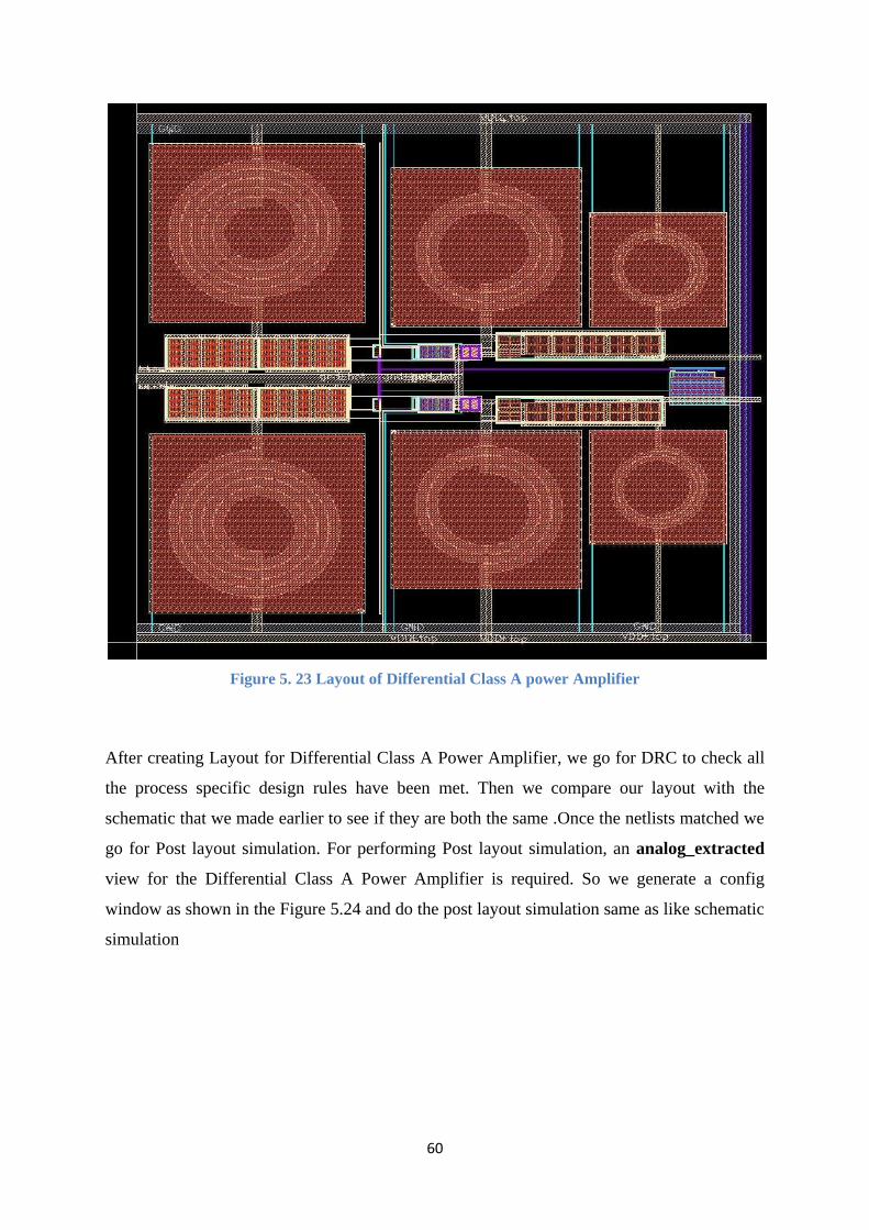
60
Figure 5. 23 Layout of Differential Class A power Amplifier
After creating Layout for Differential Class A Power Amplifier, we go for DRC to check all
the process specific design rules have been met. Then we compare our layout with the
schematic that we made earlier to see if they are both the same .Once the netlists matched we
go for Post layout simulation. For performing Post layout simulation, an analog_extracted
view for the Differential Class A Power Amplifier is required. So we generate a config
window as shown in the Figure 5.24 and do the post layout simulation same as like schematic
simulation
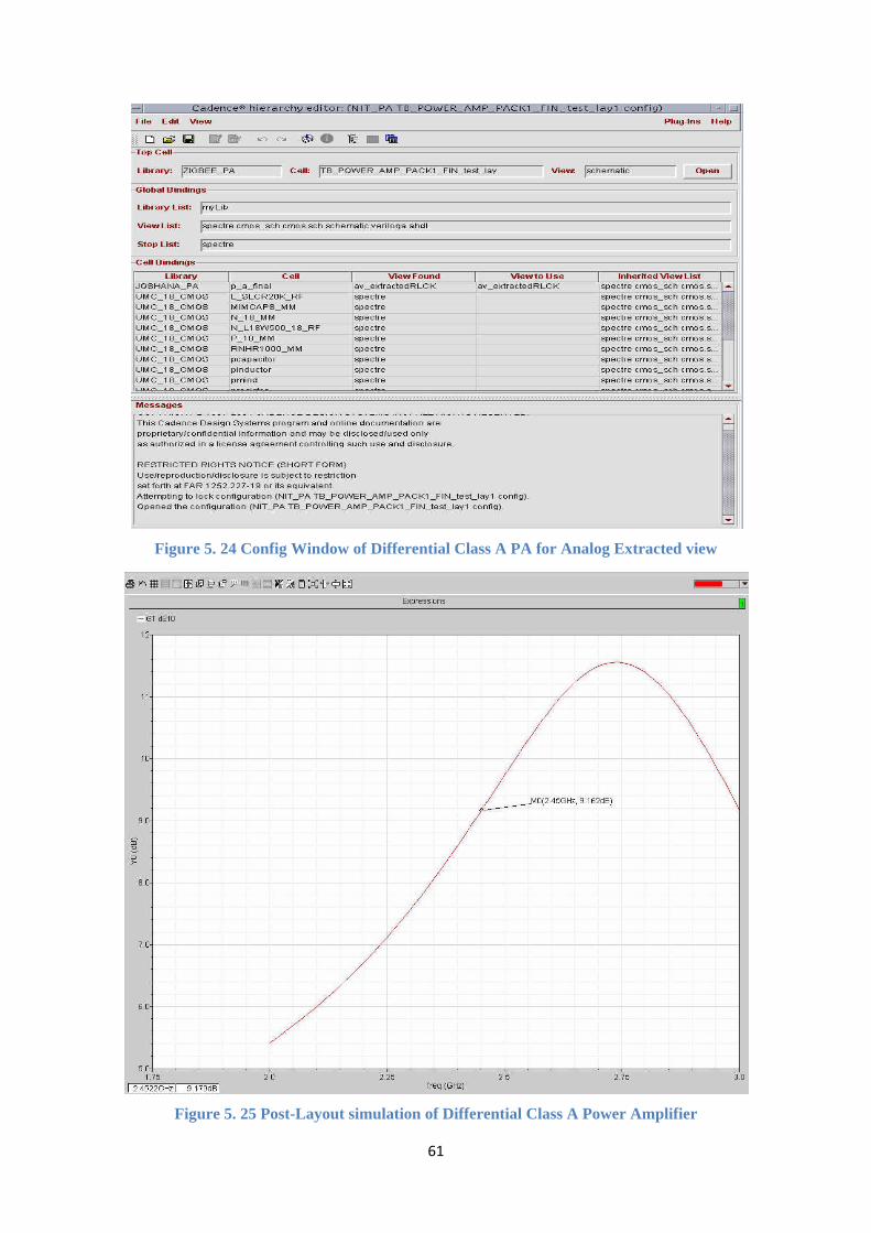
61
Figure 5. 24 Config Window of Differential Class A PA for Analog Extracted view
Figure 5. 25 Post-Layout simulation of Differential Class A Power Amplifier
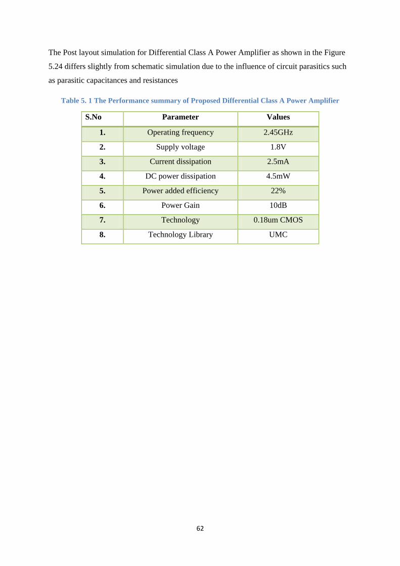
62
The Post layout simulation for Differential Class A Power Amplifier as shown in the Figure
5.24 differs slightly from schematic simulation due to the influence of circuit parasitics such
as parasitic capacitances and resistances
Table 5. 1 The Performance summary of Proposed Differential Class A Power Amplifier
S.No Parameter Values
1. Operating frequency 2.45GHz
2. Supply voltage 1.8V
3. Current dissipation 2.5mA
4. DC power dissipation 4.5mW
5. Power added efficiency 22%
6. Power Gain 10dB
7. Technology 0.18um CMOS
8. Technology Library UMC
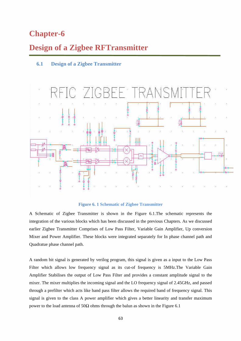
63
Chapter-6
Design of a Zigbee RFTransmitter
6.1 Design of a Zigbee Transmitter
Figure 6. 1 Schematic of Zigbee Transmitter
A Schematic of Zigbee Transmitter is shown in the Figure 6.1.The schematic represents the
integration of the various blocks which has been discussed in the previous Chapters. As we discussed
earlier Zigbee Transmitter Comprises of Low Pass Filter, Variable Gain Amplifier, Up conversion
Mixer and Power Amplifier. These blocks were integrated separately for In phase channel path and
Quadratue phase channel path.
A random bit signal is generated by verilog program, this signal is given as a input to the Low Pass
Filter which allows low frequency signal as its cut-of frequency is 5MHz.The Variable Gain
Amplifier Stabilises the output of Low Pass Filter and provides a constant amplitude signal to the
mixer. The mixer multiplies the incoming signal and the LO frequency signal of 2.45GHz, and passed
through a prefilter which acts like band pass filter allows the required band of frequency signal. This
signal is given to the class A power amplifier which gives a better linearity and transfer maximum
power to the load antenna of 50Ω ohms through the balun as shown in the Figure 6.1
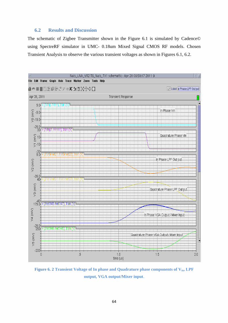
64
6.2 Results and Discussion
The schematic of Zigbee Transmitter shown in the Figure 6.1 is simulated by Cadence©
using SpectreRF simulator in UMC- 0.18um Mixed Signal CMOS RF models. Chosen
Transient Analysis to observe the various transient voltages as shown in Figures 6.1, 6.2.
Figure 6. 2 Transient Voltage of In phase and Quadrature phase components of Vin, LPF
output, VGA output/Mixer input.
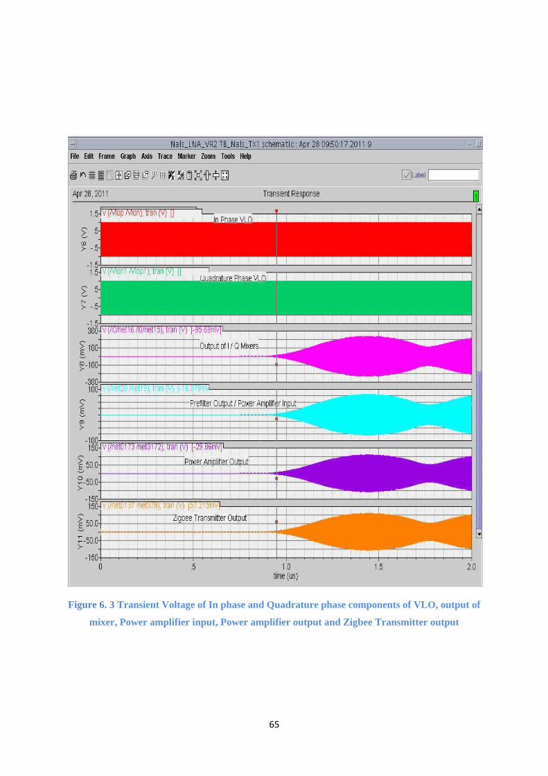
65
Figure 6. 3 Transient Voltage of In phase and Quadrature phase components of VLO, output of
mixer, Power amplifier input, Power amplifier output and Zigbee Transmitter output
66
Chapter-7
Conclusion and Future Research
7.1 Conclusion
This Thesis has provided an analysis of radio frequency building blocks for a Zigbee
Transmitter. In this work Zigbee Transmitter comprises of various blocks such as a Low Pass
Filter, Variable Gain Amplifier, Up conversion Mixer, Power Amplifier. The Low Pass Filter
allows the low frequencies and rejects all other unwanted high frequency signals.
The Variable Gain Amplifier has been discussed in Chapter 3 stabilises the output of the
Low pass filter and provide constant amplitude to the various blocks. The gain variation is of
62dB (from 40 to -22).
The RF building blocks of transmitter are Up conversion Mixer and Power Amplifier
which are discussed in Chapters 4, 5.The mixer performance is characterised and observed
the excellent performance of high linearity which gives IIP3 35.26 dBm.
The Power hungry building block of RF transmitter is Power Amplifier. Here we
designed a differential class A power amplifier to achieve linearity. The performance
parameter are characterised and observed the Power Added Efficiency is 22% and Power
gain is of 10dB.
And all these blocks were integrated and simulated using Cadence© SpectreRF simulator
in UMC-0.18um Mixed Signal CMOS RF models for the best simulation results.
7.2 Future Research
Further future research work can be done on the temperature effects and noise
performance on Variable Gain Amplifier, Up conversion Mixer and Power Amplifier of a
Zigbee Transmitter for the best results.
67
REFERENCES:
[1] A. Zolfaghari, at., “A Low-Power 2.4-GHz Transmitter /Receiver CMOS IC,” IEEE
Journal of Solid-State Circuits, vol. 38, pp. 176-183, February 2003.
[2] ZARGARI M., SU D., YUE C., ET AL.: “A 5 GHz CMOS transceiver for IEEE 802.11a
wireless LAN systems”, IEEE J. Solid-State Circuits, 2002, no. 37, pp. 1688–1694.
[3] Nam- Jin Oh and Sang-Gug Lee, ”Building a 2.4GHz radio transceiver using IEEE
802.15.4” , IEEE circuits & devices magazine November 2005, pg 43-51.
[4] Razavi, B “ RF Transmitter architectures and circuits” Custom Integrates Circuits,1999
Proceedings of IEEE 1999, 1999, pp. 197-204.
[5] Quoc-Hoang Duong, Student Member, IEEE, Quan Le, Student Member, IEEE, “A 95-
dB Linear Low-Power Variable Gain Amplifier” IEEE Trans. Circuits Syst. I Regularpapers,
vol. 53, no. 8, AUGUST 2006.
[6] W. M. Christopher, “A variable gain CMOS amplifier with exponential gain control,” in
Dig. Tech. Papers IEEE Symp. VLSI Circuits, 2000, pp. 146–149.
[7] P. Huang, L. Y. Chiou, and C. K. Wang, “A 3.3-V CMOS wideband exponential control
variable-gain-amplifier,” in Proc. IEEE Int. Symp. Circuits Syst., May 1998, pp. I-285–I-288.
[8] M. M. Green and S. Joshi, “A 1.5-V CMOS VGA based on pseudodifferential structures,”
in Proc. IEEE Int. Symp. Circuits Syst., May 2000, pp. IV-461–IV-464.
[9] C.-C. Chang, M.-L. Lin, and S.-I. Liu, “CMOS current-mode exponential- control
variable-gain amplifier,” Electron. Lett., vol. 37, no. 14, pp. 868–869, Jul. 2001.
[10]P. Kinget and M. Steyaert, “A lGHz CMOS Upconversion Mixer”, Proc. CICC, May
1996
[11]Behzad Razavi, Design of Analog CMOS Integrated Circuits, McGraw Companies,
2001.
68
[12]Yang Liu, “A 0.18um 3.3mw double-balanced CMOS active mixer”, IEEE ASIC,
july.2007.
[13] Jessica Ching-Yee Lam, 1.2V CMOS Down Conversion Mixer and VCO Design for RF
Front-end Transceiver Applications Master of Applied Science Thesis June 1996.
[14]W. Cheng, C. Chan, C. Choy, and K. Pun, “A 1.2V 900 MHz CMOS Mixer” IEEE
International Symposium on Circuits and Systems, 5:pp. 365–368, 2002.
[15] Vojkon Vidojkovic ,”Low Voltage, Low Power Folded Switching Mixer with Current
Reuse in 0.18 um CMOS”, ISCAS 2004,pp569-572
[16] Lu Liu and Zhihua Wang, “Analysis and design of a low-voltage RF CMOS mixer,”
IEEE Trans. CAS II, vol. 3, pp.212-216, Mar. 2006.
[17]S.H.-L. Tu, S. C.-H. Chen, “A 5.26-GHz CMOS Up-Conversion Mixer for IEEE 802.11a
WLAN”, IEEE International Conference on Circuits and Systems for Communications, 2008,
pp. 820– 823
[18]S.H.-L. Tu, S.C.-H. Chen “5.25 GHz CMOS cascode power amplifier for 802.11a
wireless local area network” Published in IET Microwaves, Antennas & Propagation
Received on 31st October 2007 Revised on 18th March 2008.
[19] Choi Hing Cheung, RF Power Amplifier – Class F Power Amplifier, Degree of Bachelor
of Engineering thesis May 2007.
[20] YOO C., HUANG Q: “A common-gate switched 0.9-W class-E PA with 41% PAE in
0.25 mm CMOS”, IEEE J. Solid-State Circuits, 2001, no. 36, pp. 823–830.
[21] Valentin Todorow, Impedance Matching and Matching Networks, December 2009.
[22]V. Vathulya, T. Sowlati, and D. M. W. Leenaerts, “Class-1 Bluetooth power amplifier
with 24-dBm output power and 48% PAE at 2.4GHz in 0.25-um CMOS,”Proc. Eur. Solid-
State Circuits Conf., Sept. 2001, pp.84-87
[23]TSAI K., GRAY P.R : “A 1.9 GHz, 1-W CMOS class-E PA for wireless
communications”, IEEE J. Solid-State Circuits, 1999, no. 34, pp. 962–970.
[24]Kalim, D.; Erguvan, D.; Negra, R.; , “A 1.7 GHz-to-3.1 GHz fully integrated broadband
class-E power amplifier in 90 nm CMOS,” Ph.D. Research in Microelectronics and
Electronics (PRIME), 2010 Conference, 2010, pp. 1-4.

69
[25]P.E. Allen and D.R. Holberg, CMOS Analog Circuit Design, Oxford University Press:
New York, 2002.
[26] Analog MOS Integrated Circuits for Signal Processing by Roubik Greogorian Gabor C.
Temes.