Embed Size (px)
Citation preview

NO. RIY. MO.
: ; . ~ "
ATM-912 A
ASE/CE 16 Ch. Multiplexer -A/D Converter Reliability Prediction And Failure Mode, Effects & Criticality Analysis
PAGE 1 OP /~paoe
······uem. Dlvlelon DATE 8/20/70
This ATM documents the Reliability Prediction and Failu.re Modes Effects & Criticality Analysis of the Bendix designed ASE/CE 16CH MultiplexerAID Converter. The analysis reflects the final flight configuration for the Array D ALSEP System.
Revision A clarifies the discussion of single point failure modes in Paragraph 3. 0.
Prepared by ~i2~ ALSEP Reliability Dept.
Approved by s·~ae:. ........... S. J. Ellison ALSEP Reliability Manager
16

NO. RIY.NO.
ATM 912,. A ASE/CE 16 Ch. Multiplexer-A/D Converterl----....,j'----
"'-ra•p•ce ·"··~ Dlvllllon
Reliability Predic'tion And Failure Mode, Effects & Criticality Analysis
1. 0 INTRODUCTION
PAGI 2 OP
DATI! 8/20/70
The results of the Reliability Prediction and the Failure Mode, Effects, & Criticality Analysis for the ALSEP Array D ASE/CE 16 Channel Multiplexer-A/D Converter are documented in this report. This M & A/D represents the Bendix Designed unit which makes extensive use of SSI and MSI integrated circuits and was integrated with the Active Seismic Experiment Central Electronics.
The Reliability Prediction for the 16 Channel Multiplexer is • 99995 and the Reliability Prediction for,the A/D Converter is . 99993. The overall reliability of the M & A/D is calculated to be . 99989.
2. 0 CIRCUIT DESCRIPTION
Figure 1 presents a Functional Block Diagram of the M & A/D. This diagram is included to clarify the terms and discriptions given in the Failure Mode, Effects, & Criticality Analysis portion of this ATM (Tables II & III). The numbers in each box correspond to the Circuit/ Function Item Number listed in the FMECA. Thus a clear picture may be obtained of the inter-relationships between Circuit Functions and Failure Mode Effects.
The Multiplexing Gates are the same as those used on the Array A2 and Array D 90 Channel Multiplexer, and the A/D Converter is exactly the same design as the Array D Converter except a set of Buffer-Inverters that have been added for output phase compatibility. With the above considerations, full operational capability can be confidentally expected of the Bendix Redesigned ASE/CE M & A/D.
3. 0 RELIABILITY PREDICTION
The Reliability Prediction for the 16 Channel Multiplexer is • 9999510 and the A/D Converter Prediction is • 9999343. The overall reliability for the M & A/D is calculated to be • 9998853, which is approximately equal to the design goal of • 99990. The above predictions are based on an intended lunar mission of launch, deployment, and 30 hours operation and 8730 hours standby. Figure 2 defines the Reliability Block Diagram and Mathematical Model for the Multiplexer and A/D Converter.
16

~
~
~CII.
~
_,'1-cH.
~ -, 4-CII.
/
--T1e11.
1st Tier Ch. 1-4
Incl. 1 Geo. Ch.
}._ 1 = • 00675
1st Tier Ch. 5-8 Incl. 1
Geo. Ch.
X. 2 = • 00675
1st Tier Ch. 9-12 Incl. 1 1 •
Geo. Ch.
X. 3 = • 00675
1st Tier Ch. 12-16
X-4 = .0067t
ASE/CE 16 Ch. Multiplexer-A/D Converter Reliability Prediction and Failure Mode, Effects & Criticality Analysis
110. I REV. MO. ATM-912 A
PAGE 3 or. 16
DATE 8/20/70
RT
-(}.. 1 + }.. 2 + }.. 3 + }.. 4 + }.. 5 +}.. 6 + X. 7)t = E (Any failure of any channe
RG ::::: [I - 3 }._ ~t 2 ]
2nd Tier* 1 1
X. 5 = • 0138
- (X. 5 + X. 6 + X. 7 )t E
Analog A/D
Converter
X. 6 = • 03532
(Failure of .more than one geophone channel)
Digital A/D I 0
Converter
x. 7 =. 02071
*2nd tier reliability block contains failure modes from i st tier which can cause loss of more than one geophone channel.
Failure Rate Source: Table III, }.. in units of %/1000 hrs. Standby Failure Rate = • 01 x Active Failure Rate
Figure 2 ASE/ CE M&A/D Reliability Block Diagram

~ ~' '
1alog A In _put ~
... -':: .. 16
c s
{From
'romASl
1annel :lect
ASE/CE
ASE/CE 16 Ch. Multiplexer-A/D Converter Reliability Prediction and Failure Mode, Effects & Criticality Analysis
Multiplexer and Channel Encoders
I
I
A/D Converter Digital Board
• 1st Tier 2nd Tier I -Input • Cornparato Mosfet ~ Mosfet I - Buffer Gates , ·~
Gates i I r-+
#3 ~] # I #2 rr
~I' ·~ I
~ ~ I
~ 71 I
I
Channel I Ramp Oscillator Encoder I r+ Generator Clock
I
I #4 #I
I
• I
I
I
Figure 2, ASE/CE M&A/f' '"'oeratioi)al Block Diagram
MO.ATM-912 I•EV.IIO. A
PAGE 4 OP. 16
DATE
I'-
1
I
I
I
I I
I I I I
I I I I
I
I I I I
I
-,
A/D Converter Analog Board
Counter Control
, ~I
·~ !
Counters and
Buffers
#2
~ liJ ~
NO. RIV. NO.
: : . ~. ,, ATM 912 A ;r_. 'i~.,~_ '; 0 ::~;
·······~
·,ftltemfa Dlvlelon
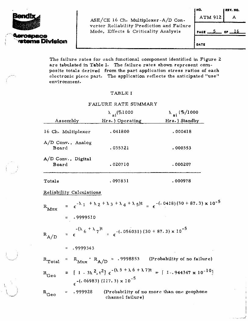
ASE/ CE 16 Ch. Multiplexer -A/D Converter Reliability Prediction and Failure Mode, Effects & Criticality Analysis PAGE 5 OF 16
DATE
The failure rates for each functional component identified in Figure 2 are tabula·ted in Table I. The failure rates shown represent composite totals derived from the part application stress ratios of each electronic piece part. The application reflects the anticipated "use'' environment.
TABLE I
FAILURE RATE SUMMARY
A .(o/olOOO a1
Assembly
16 Ch. Multiplexer
A/D Conv., Analog Board
A/D Conv. , Digital Board
Totals
Reliability Calculations
Hrs.) Operating
. 041800
• 035321
• 020710
.097831
A . (%/1000 Sl
Hr s. ) Standby
. 000418
• 000353
• 000207
• 000978
R Mux
= E-Al +A2+A3 +A 4 +A5)t = E-(.~418)(30+87.3)xl0- 5
R Geo
R Geo
= .9999510
-5 -(. 056031) (30 + 87. 3) X 10
-· E
= . 9999343
=
=
RMux • RA/D = • 9998853 (Probability of no failure)
r 1 _ 3>..2,t2J €-cAs +A 6 +A 7 >t =- r 1-.944347 x 1o- 10J -5
-(, 06983) (117. 3) X 10 E
• 999928 (Probability of no more than one geophone channel failure)

NO. RIV. NO.
: : .. '~. '.
' 1*" " ~
'·
'woapece
ASE/CE 16 Ch. Multiplexer-A/D Converter Reliability Prediction and Failure Mode, Effects & Criticality Analysis
ATM-912 A
PAGI 6 OP
··· .. "tame Division DATI! 8/20/70
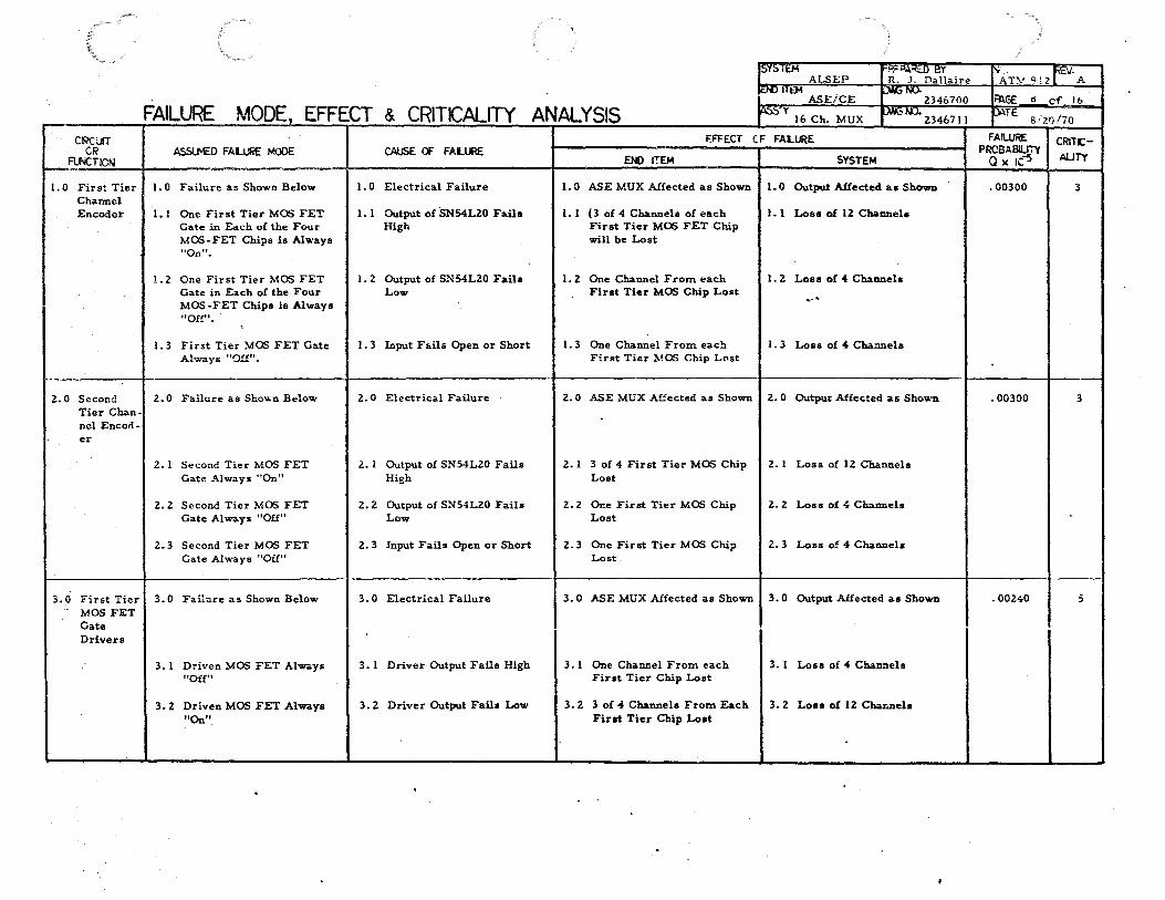
3. 0 FAILURE MODES, EFFECTS & CRITICALITY ANALYSIS
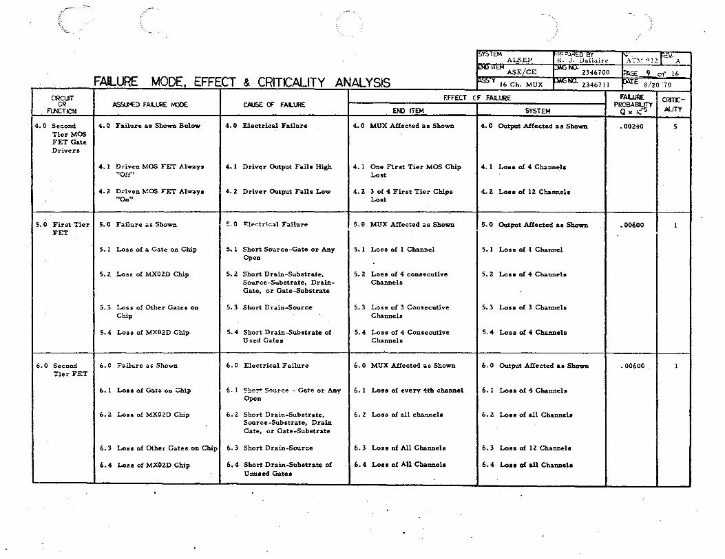
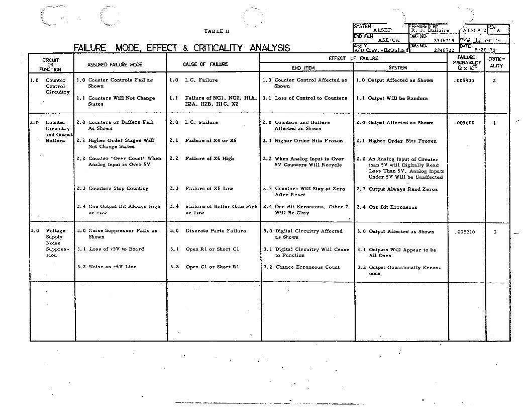
The failure mode and effects analysis for the M&A/D are documented in Tables II and III. Table II describes the functional failure modes and the resultant effects on the end item and sy~tem level. Table III delineates the failure modes at the piece part level. Each identified failure is numerically itemized for cross reference between Tables II and III, and Figure 2. (Note: the cross reference must be correlated by Assembly).
The failure probabilities reflect the identified line item. The criticality ranking lists by order of magnitude, the highest down to the lowest failure probabilities. Table II lists criticalities by circuit/function, while Table III lists the criticality sub-ranking within each circuit/ function item. With this method, the highest order criticalities are easily identified both by circuit/function levels and by discrete part levels.
The format of Tables II and III is designed to provide the reader with a narrative description of the varying types of failures that could occur, combined with the resultant performance characteristics. This information is useful to system support in performing fault isolation should an anomally occur.
The Failure Modes Effects and Criticality Analysis has shown that there is one failure mode, which constitutes an ASE Single Point Failure Mode. All 16 channels will be lost if a short occurs in the second tier MOS-FET gate package. There is absolutely no way to eliminate this failure mode since all multiplexers, regardless of the number of tiers, will have a final MOS-FET gate which can fail shorted. This failure mode is identified in Table 4, Section 6, of the Failure Mode Effects and Criticality Analysis. An intensive de- f(!_
sign effort has been made by Bendix to insure a reliable design, especially in the area of multiplex channel losses. Previous experience with the Dynatronics design has shown that 15 or 16 channels were usually lost when only one component in one channel had failed. Bendix has investigated tiering to minimize these multiple channel losses. The selected design was determined to be the best design.
There are no failure modes in the ASE/CE M& A/D which constitute an ALSEP System Single Point Failure Mode.
The selected design was also shown to have the highest reliability with respect to preserving at least two of the three Geophone channels. This is an important criteria for two reasons.
16

NO. RIY. NO.
/~pace ....... Divllllon
ASE/CE 16 Ch. Multiplexer-A/D Converter Reliability Prediction and Failure Mode, Effects & Criticality Analysis
ATM-912 A
I'AGI 7 OP
DATI 8/20/70
1) The Geophone channels are considered to be the most important from a data standpoint. Some engineering data may be returned if two or the three channels are operating while no useful engineering data is returned if more than one Geophone channel fails.
2) The Geophone channels provide a good eros s section of the 16 channels and indicate the :reliability of the complete 16 channel system.
5. 0 RELIABILITY ASSESSMENT
The purpose of pe:rfo·rming a reliability prediction and failure modes analysis is to identify inherent design weaknesses. From the :results of these analyses it has been concluded the :reliability and design objectives have been fully satisfied.
16
15Y5TEM ALSEP
·t-'.f'P~'(~ eY R. J. Dallaire f"!· r:v· AT~' "12 A l
19() I t::M ~ M). 2346700 ~GE j ASEiCE IS cf lb
FAILURE MODE, EFFECT & CRITICALITY ANALYSIS ~-y 16 Ch. MUX !-NWb MJ. 2346 711 ~TE s :zo/70 I
CIRCUIT F:FFECT CF FALURE FAILURE CRITIC- j
CR ASSUYED FALURE MODE CAUSE OF FALURE PRCBABIUTY AUTY I A.lNCTICN END ITEM SYSTEM Q X IC-5
I. 0 First Tier 1. 0 Failure as Shown Below 1. 0 Electrical Failure 1. 0 ASE MUX Affected as Shown 1. 0 Output Affected as Shown . 00300 3 Channel I Encoder 1, I One First Tier MOS FET 1. 1 Output of SN54L20 Fails 1. 1 (3 of 4 Channels of each 1.1 Loss of 12 Channels
Gate in Each of the Four High First Tier MOS FET Chip MOS-FET Chips is Always will be Lost uon".
l.Z One First Tier MOS FET l. 2. Output of SN54L20 Fails 1. 2 One Channel From each l. 2. Loss of 4 Channels Gate in Each of the Four Low First Tier MOS Chip Lost MOS-FET Chips is Always
, .. "0!!".
'
1.3 First Tier MOS FET Gate 1. 3 Input Fails Open or Short 1.3 One Channel From each 1.3 Loss of 4 Channels I
Always "0!£11• First Tier MOS Chip Lost
' 2. 0 Second 2. 0 Failure as Shown Below 2.. 0 Electrical Failure 2. 0 ASE MUX Affected as Shown 2. 0 O..tput Affected as Shown . 00300 3 Tier Chan-nel Encod-er
2.. 1 Second Tier MOS FET 2. I Output of SN54L20 Fails 2.. I 3 of 4 First Tier MOS Chip 2. I Loss o! 12 Channels Gate Always ''On" High Lost
2. 2 Second Tier MOS FET 2.. 2. Output of SN54L20 Fails 2.. 2 One First Tier MOS Chip 2. 2 Loss of 4 Channels Gate Always "Off" Low Lost
2. 3 Second Tier MOS FET 2. 3 Input Fails Open or Short 2.3 One First Tier MOS Chip 2. 3 Loss of 4 Channels Gate Always "Off" Lost.
3. 0 First Tier 3. 0 Failure as Shown Below 3. 0 Electrical Failure 3. 0 ASE MUX Affected as Shown 3. 0 Output Affected as Shown . 002.40 5 ..
MOS FET Gate Drivers
3. I Driven MOS FET Always 3. I Driver Output Fails High 3. I One Channel From each 3. 1 Loss of 4 Channels "0££11 First Tier Chip Lost
3. 2 Driven MOS FET Always 3. 2 Driver Output Fail• Low 3. 2 3 of 4 Channels From Each 3. 2 Lou of 12 Channels
"On" First Tier Chip Lost
-- -- -- - -
SYSTEM P.~"'~-<i:.p_ f!Y ~-- ="" ALSEP }{. J. !Jallair" AT~~ \ll:! r- · ~;. e«> 1'"'-"' ASE/CE ~ MJ. Z346700
-~SE 9 CT- 16
FAILURE MODE, EFFECT & CRITICALITY ANALYSIS p::,s·y 16 Ch. MUX fJNI:> NU, Z3 46 7 II p.\TE s/zo '7o
ClRClJT F.FFECT CF FAIL~E F~ CRITK:-CR ASSlJIIEO FALUI<E MODE CAUSE OF FALURE PRCSABIUrY
AUTY FU!IICTICN END ITEM SYSTEM Q x IC~
4.0 Second 4. 0 Failure as Shown Below 4. 0 Electrical Failure 4. 0 MUX Affected as Shown 4. 0 Output Affected as Shown . 00240 5 Tier MOS FET Gate Drivers
4.1 Driven MOS FET Always 4- 1 Driv~r Output Fails High 4. 1 One First Tier MOS Chip 4. 1 Loss of 4 Channela ''CYJ" Lost
4. 2 Driven MOS FET Always 4. 2 Driver Output Fails Low 4. Z 3 of 4 First Tier Chips 4. Z Lou of 12 Channels "On" Lost
5. 0 First Tier 5. G Failure as Shown 5.0 !:!Petrical Failure 5. 0 MUX Affected as Shown 5. 0 Output Affected as Shown .00600 1 FET
5.1 Loss of a Gate on Chip 5.1 Short Source-Gate or Any 5. I Loss of I Channel 5.1 Loss of I Channel Open
5. 2 Loss of MXOZD Chip 5. 2 Short Drain-Substrate, 5. Z Loss of 4 consecutive 5. 2 Loss of 4 Channels Source-Substrate, Drain- Channels Gate, or Gate-Substrate
5.3 Loss o! Other Gates on 5. 3 Short Drain-Source 5.3 Loss of 3 Consecutive 5.3 Loss of 3 Channels Chip Channels
5.4 Loss of MXOZD Chip 5. 4 Short Drain-Substrate of 5. 4 Loss of 4 Consecutive 5. 4 Loss of 4 Channels Used Gates Channels
6.0 Second 6.0 Failure as Shown 6. 0 Electrical Failure 6. 0 MUX Affected as Shown 6. 0 Output Affected as Shown • 00600 I Tier FET
6.1 Loss of Gate on Chip ~- 1 Short Source - Gate or Any 6. 1 Loss of every 4th channel 6.1 Loss of 4 Channels Open
6. 2 Loss of MX02D Chip 6. 2 Short Drain-Substrate, 6. Z Loss of all channels 6. 2 Loss of all Channels Source-Substrate, Drain Gate, or Gate-Substrate
6. 3 Loss of Other Gates on Chip 6. 3 Short Drain-Source 6.3 Loss of All Channels 6.3 Loss of 12 Channels
6.4 Loss of W.X02D Chip 6. 4 Short Drain-Substrate of 6.4 Loss of All Channels 6. 4 Lou qf all Channels Unused Gates
---·-

CIRCUIT CR
Fl.JNCT!CN
TABLE II
FAILURE MODE, EFFECT & CRITICALITY
ASSUMED FAILURE MODE CAUSE OF FALURE
ANALYSIS
!SYSTEM ~P."P~~i:.D BY A LSEP I R. J. Dallaire
iniTITi:J.l ,~ ~. ;- .. ASE/CE -.23!l6700
l~b~w.-AnalQJZ.Br~NO. 2.346719
EFFECT CF FALURE
END ITEM SYSTEM
1. 0 Oscillator- II. 0 Oscillator Fails as Shown Clock
I. 0 Failure of Discrete Parts or Integrated Circuits
I. 0 Clock Affected as Shown • 0 Output Affected as Shown
l. 1 Oscillator Fails to Provide Output
1. 2 Oscillator Frequency Drift
1.1 Short or Open RI, R2, R3, R4JI.l Loss of Clock to Counters IJ..I Outp.rt will be Frozen R5, Cl, C2, Yl, or Failure ofNGlA, NGIB, NGIC
1. 2 Crystal (YI) Parameter Drift JI. 2 Counters Will Count at Wrong fl. 1 Output Slightly High or Low Speed
2. 0 Input Bu£ferj2. 0 Buffer Fails as Shown 2. 0 Failure of 1. C. or "Capacitor lz. 0 Analog Input Affected as Shown
2. 0 Output Affected as Shown
3. 0 Cornparato (Compares Ramp Voltage to Analog Input Voltage)
~ .• I Loss of Input to Comparator 2.. I Short C4, Failed Output of Jz. I Analog Input Appears High or ~·I Output all l's or O's
LMI02 ~ Low r· 2 Offset Input to Comparator 2.. 2 Input Offset Drift of LMI02 • 2 Offset Input Voltage • 2 Slight Error in Output
!2. 3 Noise to Input of Comparator 2. 3 Open C4 • 3 Chance of Small Errors in • 3 Occassional Error in Output
3. 0 Comparator Fails as Shown
3. I Loss of Command Latch Signal
3. 2 Comparator Will Switch too Soon or too Late
3. 3 Noise in Comparator
3. 0 Failure of Discrete Parts or 1. C.'s
3. I Open R5, RI3, or short R6, C7, or failure of LMIII, X5.
3. 2 LMIII Input Offset Drift
3. 3 Open C5 or short Rl2
Conversion
~. 0 Ramp Coinparison Affected
3. I Counters Will Count Erroneously
~. 0 Output Affected as Shown
~. I Output will be Random or AU Zeros
p. 2 Count Will be Slightly too High r· 2 Output will be Slightly High or or too Low Low
~. 3 Chance Count Will be Low ~. 3 Occasional Slightly Low Output
p::v. .o\T~1 0]2 I A
~GE 10 cf 16
P·-;:-M.- 8/20 iiO
FAILURE I CRITlC-PRCBA~ AI.JTY
Q x IC
• 007313 2
.004507 4
.004833 3

TABLE II JSYS TEM ~P; P.),~l..lJi!Y L AI.SEP R. J. Dallaire lp..rl iTt_.., 1~ MJ.-L ASE/CE 2346#00
~:.:.-ni OJzF·A ~..-£ 11 Cf Jt
FAILURE MODE, EFFECT & CRITICALITY ANALYSIS ~·y· DM:W t-\/U Conv. -Analog Br<ij · • 2346719 ~~Tt.h/Z·J 70
~lJT OR
Fl.N:TICN ASSI.KD FAL~ M00E CAUSE OF FAILURE
4. 0 Ramp r· 0 Ramp Generator Fails as Slownf!. 0 Failure of Discrete Devices Generator Shown I or I. C.
• 1 Ramp Generator Will Cease to Function
~· Z Incorrect Ramp Slope
• 1 Open or Short RS, R9, RIO, Rll, Rl4, RlS, C3, CRZ, Ql Open R7, or LM107 Failure
~- Z Drift of CRZ, RS, R9, RHl, Rll, C3, or Input Offset Drift of LM107
• 3 Excess Current in Zener CRl j.l. 3 Short R7
EFFECT
END ITEM
4. 0 Ramp Generator Affected as Shown
4.1 Counter Will Not Turn Off
4. Z Counter Turned Off too Soon or too Late
4. 3 -IZV Supply May Be Shorted
CF FAILURE
SYSTE~
!4. 0 Output Affected as Shown
4. 1 Output Will Be Random
4. Z Output Slightly High or Low
4. 3 Possible Loss of AID Con- ' verter (Will Cause PDU to Switch to Redundant AID Converter)
5.0 Power Supply
15.0 On-Board Supplies Affected as Shown
5. 0 Failure of Capacitors as Slx>wnl5. 0 On-Board Supplies Affected As Shown
5. 0 Output Affected as Shown
Noise SuppressioJ:;. 1 Loss of -lZV or +5V Lines
5. Z Noise on +12V, -lZ, or SV Lines
5. 1 Short C8 or C9
5. 2. Open C6, C7, CS, or C9
5. 3 Loss of +lZV Line Capacitor IS. 3 Short C6 or C7
6. 0 Thermisto16. 0 Thermistor Affected as Shown 6. 0 Resistor Failures as Shown Network
6. 1 Improper Voltage Supplied to 6. 1 Open or Short Rl6, R7 Thermistors
6. Z Drift in Voltage Supplied to 16. Z Drift Rl6, Rl7 Thermistors
5. 1 Loss of One MUX -AID Conv. IS. 1 Loss of One AID Converter
5. Z Chance Erroneous Count
5. 3 No Effect Due to Redundant Capacitors
5. Z Occasional Output Error
5. 3 No Effect
16.0 Thermistor Readings Affected 16.0 AID Converter Operation as Shown not Affected
6. 1 Thermistor Readings Offscale 6. 1 Thermistor Offscale High or Hi~;h or Low Low
6. 2. Thermistor Readings Slightly 6. 2. Thermistor Slightly High or High or Low Low
FAilURE PRCBABI!..rrY ax 1c-->
.017864
.000804
I . 000335
CRlTIC
ALITY
5
6
"TABLE II SYSTEM Al.SEP ffFP~~E~,~ R. J. allaire ~T:\1 QJ2r~·A OO ITtl'f ASEICE :w:, NQ.
234671Q i=n';;: 12 ('of ·~
FAILURE MODE. EFFECT & CRITICALITY ANALYSIS ~COnv.-Il~italBrd p.t.t;:.l\0. 2346722 ~TE 8 iz0/70
CRCIJT F.FFECT CF FALURE FALURE CRITIC-PRCBASll.ITY CR AS5LMED FALURE MODE CAUSE OF FAUIRE
END ITEM SYSTEM Q x IC"'5 AUTY FLNCTICN
1.0 Counter I. 0 Counter Controls Fail as 1.0 I. C. Failure l. 0 Counter Control Affected as 1. 0 Output Affected as Shown .005900 2 Control Shown Shown Circuitry.
1. 1 Counters Will Not Change I. 1 Failure of NGl, NG2, HlA, 1. 1 Loss of Control to Counters I. 1 Output Will be Random States H2A, H2B, HI C, X2
z.o Counter 2. 0 ·Counters or Buffers Fail 2.0 I. C. Failure 2. 0 Counters and Buffers 2. 0 Output Affected as Shown .009600 1 Circuitry As Shown Affected as Shown and Output Buffers 2. 1 Higher Order Stages Will 2. 1 Failure of X4 or X5 2. 1 Higher Order Bits Frozen 2. 1 Higher Order Bits Frozen
Not Change States
2. 2. Counter "Ov~!" Count .. When 2.2 Failure of X6 High 2. 2 When Analog Input is Over 2. 2. An Analog Input of Greater Analog Input is oVer SV SV Counters Will Recycle than SV will Digitally Read
Less Than 5V, Analog Inputs Gncer 5V Will be Unaffected
2·. 3 Counters Stop Counting 2.3 Failure of X6 Low 2. 3 Counters Will Stay at Zero 2. 3 Output Always Read Zeros After Reset
!
Z. 4 One Output Bit Ab1:ays High 2.4 Failure of Buffer Gate High 2. 4 One Bit Erroneous, Other 7 2. 4 One Bit Erroneous or Low or Low Will Be Okay
3.0 Voltage 3. 0 Noise Suppressor Fails as 3.0 Discrete Parts Failure 3. 0 Digital Circuitry Affected 3. 0 Outp.:.t Affected as Shown • 0052.10 3 Supply Shown as Shown Noise Sl..O.ppres- 3. 1 Loss of +5V to Bo-.rd 3. 1 Open Rl or Short Cl 3. 1 Digital Circuitry Will Cease 3. 1 Outputs Will Appear to be sion to Function All Ones
3. 2 Noise on ~5V Line 3.2 Open Cl or Short Rl 3. 2 Chance Erroneous Count 3. 2 Output Occasior.ally Erron-eous
-
-
-----·-~--------- ·--.. ---~-.........._ ..... ~-

'~"1\BLE III f:)YSTEM
ALSEP R.:'"' J ~oa'Nair<> ~~- F· AT.M OJ2 A
~ !TIM ASE,.CE pWG 1«}2346 700 PAGE 13 of 16
FAILURE MODE, EFFECT & CRITICALITY ANALYSIS WORKSHEET !Af'6::.·th. Multiplexer ~ M). 2346711 ~TE8/ZO ~n
~RT /a:M>Ot£NT EFFECT OF FAILURE FAILURE CRITIC-FAILURE MODE PR8BABI~TY ALITY
S't'MSOL {a.) ASSEMBLY END ITEM X 10
1.0 First Tier Chan- • I Output of SN54LZO Fails High (.400) 1. I One First Tier MOS FET Gate in Each 1. I Loss of 12 Channels, (3 of 4 Channels .0012 I** nel Encoders of the Four MOS-FET Chips is Always of each First Tier MOS FET Chip wil
(SN54L20) "On". be Lost)
• 2 Output of SN54L20 Fails Low (.400) 1. 2 One First Tier MOS FET Gate in Each I. 2 Loss of 4 Channels, (One Channel .0012 I of the Four MOS-FED Chips is Always From Each First Tier MOS Chip) "Off".
. 3 Input Fails Open or Short (.200) I. 3 First Tier MOS FET Gate Always l. 3 Loss of 4 Channels (One Channel • 0006 2 "Off". From Each First Tier MOS Chip)
2. 0 Second Tier • 1 Output of SN54LZO Fails High (.400) Z. I Secor.:! T~e=- ... !OS FET fJate Always ~.I '.o• • of 12 Channels (l of 4 Firat Tie .0012 1** I Channel Encoders uonn MOS Chips) (S~54LZO)
• 2 Output of SN54L20 Fails Low (.400) 2. 2 Second Tier MOS FET Gate Always 2. 2 Loss of 4 Channels (One First Tier • 0012 1 "Off" MOS Chip
. 3 Input Fails Open or Short (. 200) 2. 3 Second Tier MOS FET Gate Always 2. 3 Loss of 4 Channels (One First Tier .0006 2
' "Off" MOS Chip)
. 3. 0 First Tier MOS 3. 1 Output Fails High (.500) 3. 1 Driven MOS FET Always "Off" 3. 1 Loss of 4 Channels (One Channel .0012 1
FET Gate Driver From Each First Tier Chip) (OM 7800)
3. 2 Output Fails Low (. 500) 3. 2 Driver MOS FET Always "On'' 3. 2 Loss of 12 Channels (3 of 4 Channels .0012 1** From Each First Tier Chip)
4. 0 Second Tier ~. 1 Output Fails High (. 500) 4. I Driver MOS FET Always "Off" 4. I Loss of 4 Channels (One First Tier • 0012 1 MOS FET Gate MOS Chip) Drivers (DM7800
I 4. 2 Output Fails Low (. 500) 4. 2 Driver MOS FET Always "Cn" 14.2 Loss of 12 Channeb (3 of 4 Firat .0012 1**
---- -----------Tier Chips)
--------- --
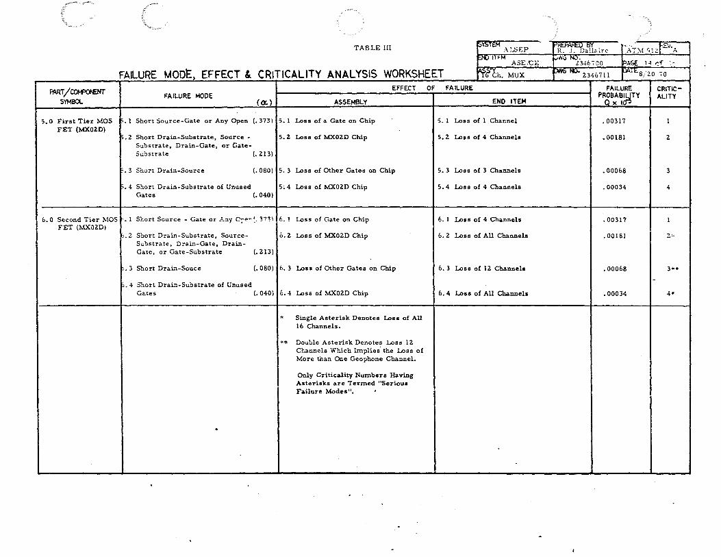
TABLE III j5YSTEM _-\ LSEP
~ tTFM ASE-tE
FAILURE MODE, EFFECT & CRITICALITY ANALYSIS WORKSHEET rr~·h. MUX
FAAT/~ SYMSOL
EFFECT OF FAILURE FAILURE MODE
((X.} ASSEMBLY
5. 0 First Tier MOS fi. l Short Source-Gate or Any Open (. 373 J IS. l Loss of a Gate on Chip FET (MX02D)
f>· 2 Short Drain-Substrate, Source - fS. 2 Loss of MXOZD Chip Substrate, Drain-Gate, or Gate-Substrate (. 213)
• 3 Short Drain-Source (. 080) 5. 3 Loss of Other Gates on Chip
• 4 Short Drain-Substrate of Unused 5; 4 Loss of MX02D Chip Gates (.040)
6. 0 Second Tier MOSt· l Sioort Source - Gate or A:1y C!'"~ ~- '373\ 6. l Loss of Gate on Chip FET (:MX02D) I
·. 2 Short Drain-Substrate, Source- o. 2 Loss of MX02D Chip Substrate, Drain-Gate, Drain-Gate, or Gate-Substrate (.213)
fo. 3 Short Drain-Souce (. 080) 16. 3 Loss of Other Gates on Chip
t'· 4 Short Drain-Substrate of Unused Gates (. 040) 16. 4 Loss of MX02D Chip
* Single Asterisk Denotes Loss of All 16 Channels.
** Double Asterisk Denotes Loss 12 Channels Which Implies· the Loss of More than One Geophone Channel.
Only Criticality Numbers Having Asterisks are Termed "Serious Failure Modes", •
END ITEM
5. l Loss of l Channel
5. 2 Loss of 4 Channels
,5. 3 Loss of 3 Channels
5. 4 Loss of 4 Channels
6. l Loss of 4 Channels
I 6. 2 Loss of All Channels
I 6. 3 Loss of 12 Channels
6. 4 Loss of All Channels
-u....r-.""""-'-' BY R. J. Dalla;re ·~.\-T:v! <; l zf2"' A
p ... ~ l·"-~h .. 6700 !PAGE 1-1 r;;f '·
pN6 NO. 2346711 pt'TE.B/20 70
FAILURE PROBABILJTY _Q_x I~
• 00317
• 00181
.00068
• 00034
• 00317
. 00181
.00068
.00034
CRITICALITY
2
3
4
z::
3"'*
4*

TABLE III f:>ThTEM ALSEP It~' :r: "''a!Kire ~
1
T'.I OJ2 F· A
~ ITEM A<'SlCE f-l'VI) NU. 234f>7C'C' ~'.r~e ~ :: f f ~ (.
FAILURE MOD~, EFFECT & CRITICALITY ANALYSIS WORKSHEET ~S~YConv. Analog BI<; f.N«:'I'U· 2.3467J'J 1'-»'lc.s 20 70
FAAT /CCH'Ot£NT EFFECT OF FAILURE FAILURE CRITIC-FAILURE MODE PROBABILITY ALITY SYMOOL ( oc) ASSEMBLY END ITEM Q x to-5
:.o Oscillator 1.1 Short or Open Rl, R2, R3, R4, R5, 1. 1 Oscilaltor Will Fail to Provide Output 1. 1 Loss of Clock to Counters .004313 1 Cloc;.: Rl, R2, Cl, CZ, Yl, or Failure of NGlA, 3.3, R4, R5, Cl. NG1B, NGIC (. 533) C2, Y1, ~GlA, ~GlB, NG1C I. 2 Crystal (Y 1) Drift (. 371) l. 2 Oscillator Frequency Drift 1. 2 Counters Will Count at Wrong Speed .003000 2
2.0 L'1put Buffer: 2. 1 Short C4, Output LM102 (. 776) 2. 1 Loss of Input to Comparator 2. 1 Analog Input Appears High or Low .003503 1 :..C\-11 0 2 , C4
2. 2 Input Offset Drift (. 193) 2. 2 Offset Input to Comparator 2. 2 Offset Input Voltage .000870 2
2. 3 Open C4 (.030) 2. 3 Noise to Input of Comparator 2. 3 Chance of Small Errors in Conversion . 000134 3
3. 0 Comparator: 3. I Open Rl2, Rl3, Short Rl3, C5; 3. 1 Loss of Command Latch Signal 3. 1 Counters Will Count Erroneously .004020 1 Rl2, Rl3, CS, Failure of LM111, XS (. 798) LM111, XS -3. 2 LM111 Input Offset Drift (. 140) 3. 2. Comparator Will Switch too Soon or 3, 2 Count Will be Slightly too High or • 000810 2
too Late too Low
3. 3 Open C5, Short R12 (. 002.) 3. 3 Noise in Comparator 3, 3 Chance Count Will be Low .000003 3
~- 0 Ramp Generatpr: 4.1 Open or Short R8, R9, RIO, Rll, 4. 1 Ramp Generator Will Cease to 4. 1 Counter Will Not Turn Off • 009248 1 :a.7, R8, R9, RIO Rl4, R15, C3, CR2, Ql, Open R7, Function Rll, Rl4, Rl5, or Output Failure of LM1 07 (.442) C3, Cl2, Ql, LMI07 4,2 DriftofCRZ, R8, R9, RIO, Rll,
413) 4. 2 Incorrect Ramp Slope 4. 2 Counter Turned Off too Soon or too .008631 2
Late ' 4. 3 Short R7 (. 001) 4, 3 Excess Current in Zener CR1 4. 3 -1 ZV Supply May Be Shorted . 00003 3
s.o Supply Noise 5. 1 Short C8, C9 (. 070) 5.1 !..os~of-12Vor +SV 5, 1 Loss of One MUX-A/D Converter • 000060 2 Suppression C6, C7, C8, 5. 2 Open C6, C7, C8, C9 (. 798) 5. 2 Noise on +12, -12, & +SV Lines 5, 2 Chance of Erroneous Count .000684 1 C9
5. 3 Short C6, or C7 (. 070) 5. 3 No Effect Due to Redundant Capacitor 5. 3 No Effect • 000060 2
6.0 Thermistor 6. I Open or Short R16, R17 (. 817) 6. 1 Thermistors Not Supplied Proper 6. 1 Incorrect Thermistor Outputs Network: RI6, Voltages • 000274 1
R17 6,2 Drift R16, Rl7 (. 183) 6. 2 Thermistors Not Supplied Exact 6, 2 Slight Error in Thermistor Outpute .000061 2 Voltages --
~'I'STEJ\1 A LSEP Bl' r-o:;. F-EV. R. '· Dallaire I A~o.! GJ2j__ A
~ IT"M ASE/CE pwG NO. 2 j 3 t;"uu ;..: .. <:.E ;;, vf i<;
FAILURE MODE, EFFECT & CRITICALITY ANALYSIS WORKSHEET. ~~\Y,..._ r.rt· 1 B d DW6 NO. 6-~ 1041 ::. lA! v VJI'N • ..,.;lta r • r 234 ~~~ I s 20 70
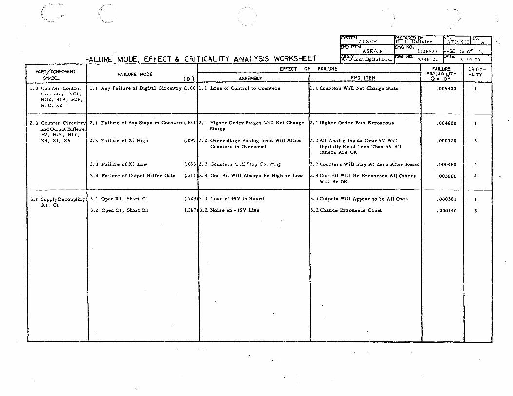
FAAT/COM?Ot£NT SYMBOL
1. 0 Counter Control Circuitry: NGl, NGZ, HlA, HZB, HIC, X2
Z. 0 Counter Circuitry and Output B.Ufers HZ, HIE, HIF, X4, X5, X6
EFFECT OF FAILURE FAILURE MODE
( 0:.) ASSEMBLY
1.1 Any Failure of Digital Circuitry (1.0011.1 Loss of Control to Counters
2. 1 Failure of Any Stage in Counters' 63112. 1 Higher Order Stages Will Not Change States
2. 2 Failure of X6 High
z. 3 Failure of X6 Low
(.095 tz. 2 Overvoltage Analog Input Will Allow Counters to Overcount
(.06312. 3 Cvun.te1 S ".'.":~ CtO? c..,•:"'! .. i~g
END ITEM
1. 1 Counters Will Not Change State
~· 1 Higher Order Bits Erroneous
~. Z All Analog Inputs Over 5 V Will Digitally Read Less Than 5V All Others Are OK
? . ~ Cou-,ters Will Stay At Zero After Reset
2. 4 Failure of Output Buffer Gate (,Zll jz. 4 One Bit Will Always Be High or Low Jz. 4 One Bit Will Be Erroneous AU Others Will Be OK
3.0 SupplyDecoupling~ 3.1 Open Rl, Short Cl Rl, Cl
(.7Z9t3. 1 Loss of +SV to Board 3. 1 Outputs Will Appear to be All Ones,
3. Z Open Cl, Short Rl (.Z67i3.Z Noise on -15V Line 3. Z Chance Erroneous Count
FAILURE PROSABl~fY
Q X 10
• 005400
.004800
.000720
.000480
. 003600
.000381
.000140
CRITicALITY
3
.i
2
z