Embed Size (px)
Citation preview

01.03.2001Page 1
Michael HartenbergerUniversity of Cottbus
Lars ChristophAndreas SteinbachCenter forDevelopment andInnovation
Infineon TechnologiesDresden
ProjectPULSAR
APCAPC
2nd AEC/APC Conference Europe, April 18th-20th 2001, Dresden
Arcing prevention by dry clean optimizationat Shallow Trench Isolation (STI) Etch inAMAT MxP by use of plasma parameters
Michael Hartenberger [email protected]
University of Cottbus www.tu-cottbus.de
Lars Christoph [email protected] Steinbach [email protected] for Development and InnovationInfineon Technologies Dresden www.infineon.com

01.03.2001Page 2
Michael HartenbergerUniversity of Cottbus
Lars ChristophAndreas SteinbachCenter forDevelopment andInnovation
Infineon TechnologiesDresden
ProjectPULSAR
APCAPC
2nd AEC/APC Conference Europe, April 18th-20th 2001, Dresden
Acknowledgement
q The authors of this poster would like to thankSiegfried BernhardInes UhligAstrid KretschmarThomas KuenzelmannInfineon Technologies Dresden, Germany
q The work for this paper was supportedØ by the EFRE fund of the European CommunityØ and by funding of the State Saxony of the Federal Republic of
Germany, project PULSAR, project number 5706.
q The authors are responsible for the content of the paper.
Acknowledgement

01.03.2001Page 3
Michael HartenbergerUniversity of Cottbus
Lars ChristophAndreas SteinbachCenter forDevelopment andInnovation
Infineon TechnologiesDresden
ProjectPULSAR
APCAPC
2nd AEC/APC Conference Europe, April 18th-20th 2001, Dresden
Outline
q Introduction –Shallow Trench Isolation (STI) etch process
q Arcing at STI etch in AMAT MxP chamberq SEERS measurement techniqueq Development of a new dry clean using plasma
parameters for real time process monitoringØ Basic experiments (not shown in this publication)Ø Optimization of clean stepØ Optimization of conditioning stepØ Optimization of clean-/conditioning timeØ Long term evaluation
q Summary
Outline

01.03.2001Page 4
Michael HartenbergerUniversity of Cottbus
Lars ChristophAndreas SteinbachCenter forDevelopment andInnovation
Infineon TechnologiesDresden
ProjectPULSAR
APCAPC
2nd AEC/APC Conference Europe, April 18th-20th 2001, Dresden
STI etch process - Overview
ResistARCSiN
Si
deeptrench
a) Starting profile b)
ResistARCSiN
Si
Mask-open step
ResistARCSiN
Si
c) Trench etch step
SiN
Si
Oxid
d) Oxide CVD f) A-B:top-CD bottom-CDOxide
SiN
Si
Oxide
e) Planarization
A
B
Introduction - STI etch process
01.03.2001Page 5
Michael HartenbergerUniversity of Cottbus
Lars ChristophAndreas SteinbachCenter forDevelopment andInnovation
Infineon TechnologiesDresden
ProjectPULSAR
APCAPC
2nd AEC/APC Conference Europe, April 18th-20th 2001, Dresden
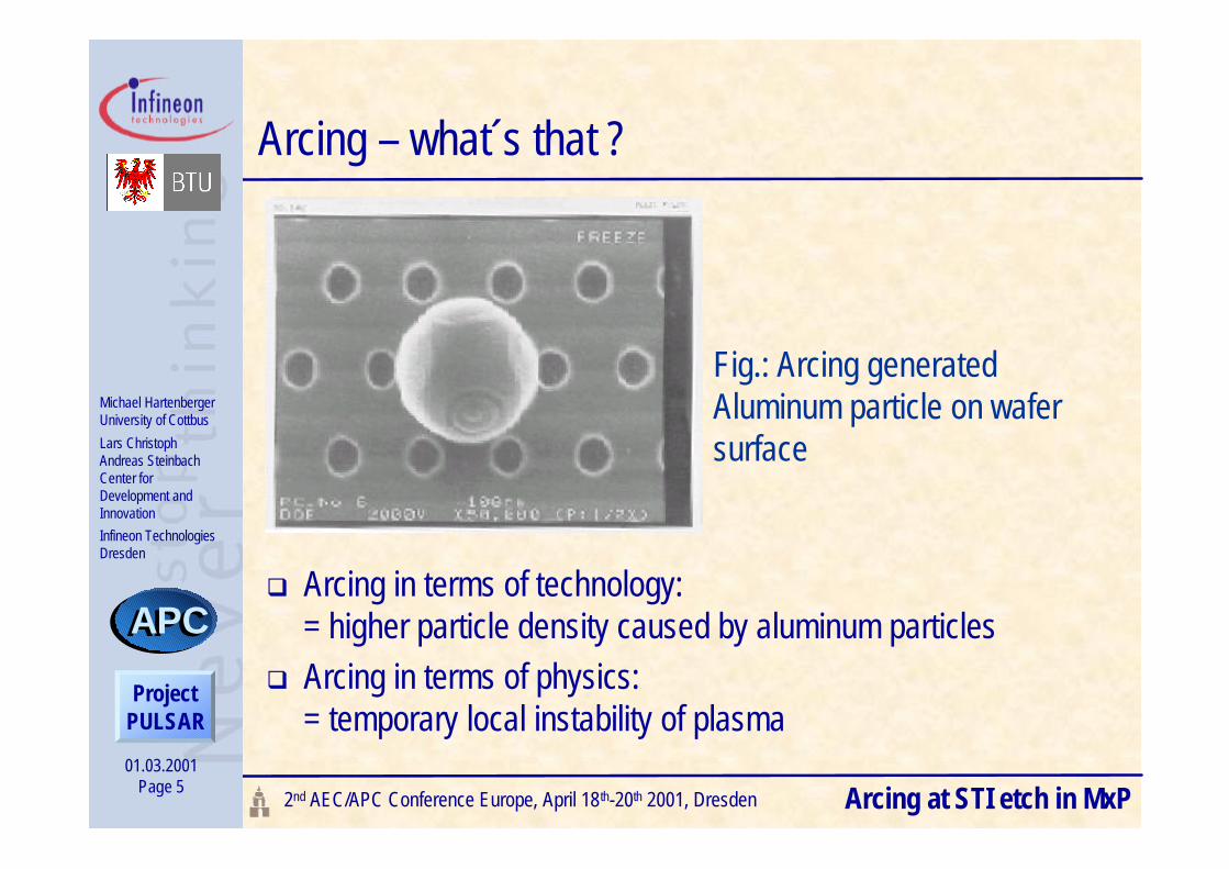
Arcing – what´s that ?
q Arcing in terms of technology:= higher particle density caused by aluminum particles
q Arcing in terms of physics:= temporary local instability of plasma
Arcing at STI etch in MxP
Fig.: Arcing generatedAluminum particle on wafersurface

01.03.2001Page 6
Michael HartenbergerUniversity of Cottbus
Lars ChristophAndreas SteinbachCenter forDevelopment andInnovation
Infineon TechnologiesDresden
ProjectPULSAR
APCAPC
2nd AEC/APC Conference Europe, April 18th-20th 2001, Dresden
Why Arcing at STI etch in our AMAT MxPchambers appeared
q Basic reasons for arcing:Ø Hardware defects (i.e. scratches)Ø Normal waste of anodizationØ Potential differences between chamber partsØ Critical process conditions (i.e. high RF power, polymers)
q Main arcing reason at STI etch in our MxP chambers:Ø Change of product mix: a new product uses a high polymerizing
etch chemistryè The usual dry clean was not efficient enough for the new
process mix, thicker polymer layers at the chamber wallè Arcing !
Arcing at STI etch in MxP

01.03.2001Page 7
Michael HartenbergerUniversity of Cottbus
Lars ChristophAndreas SteinbachCenter forDevelopment andInnovation
Infineon TechnologiesDresden
ProjectPULSAR
APCAPC
2nd AEC/APC Conference Europe, April 18th-20th 2001, Dresden
How to get rid of arcing at STI etch in AMAT MxPchamber ?
q Extending clean time or increasing gasflows for the standardclean recipe is not a viable solution. It caused two effects:Ø Less arcing, yes.Ø But also a very strong first wafer effect on critical dimensions of
product wafers, which could not be tolerated !
è Development of a new dry clean recipe was necessary:ØWith effective polymer reduction on chamber walls.Ø And with small tolerable CD degradation on product wafers.
è Development of a new dry clean using a different gas mixture.
Arcing at STI etch in MxP

01.03.2001Page 8
Michael HartenbergerUniversity of Cottbus
Lars ChristophAndreas SteinbachCenter forDevelopment andInnovation
Infineon TechnologiesDresden
ProjectPULSAR
APCAPC
2nd AEC/APC Conference Europe, April 18th-20th 2001, Dresden
Strategy to develop a new dry clean
q 1. Basic experiments:Ø Test of other gas mixtures, e.g. CF4/O2, using resist test wafersØ Target: High polymer etch rate
q 2. Evaluation of the new dry clean on product wafers:Ø Target: First wafer effect (critical dimensions !) negligible.
q 3. Long term evaluation of new dry clean on product wafers:Ø Target: New dry clean must be efficient enough
q Optimization between long term clean effect and first wafereffect on critical dimensions
q For the efficient development of the new dry clean we useda „quick and dirty“ real time in- situ process monitor -SEERS.
Development of new dry clean

01.03.2001Page 9
Michael HartenbergerUniversity of Cottbus
Lars ChristophAndreas SteinbachCenter forDevelopment andInnovation
Infineon TechnologiesDresden
ProjectPULSAR
APCAPC
2nd AEC/APC Conference Europe, April 18th-20th 2001, Dresden
Principle of SEERS
q Self Excited Electron PlasmaResonance SpectroscopyØ Passive electrical methodØ Integral physical parameters
RF currentRF voltage
RF currentRF voltage
FFTFFT
Model SEERSModel SEERS
Electron collision rateElectron density
Bulk powerDC bias voltage
Electron collision rateElectron density
Bulk powerDC bias voltage
Development of new dry clean

01.03.2001Page 10
Michael HartenbergerUniversity of Cottbus
Lars ChristophAndreas SteinbachCenter forDevelopment andInnovation
Infineon TechnologiesDresden
ProjectPULSAR
APCAPC
2nd AEC/APC Conference Europe, April 18th-20th 2001, Dresden
Experiments to optimize the new dry clean
q The new CF4/O2 dry clean recipe consists of two parts (like old one):Ø 1. Clean step – to remove the polymerØ 2. Conditioning step – to minimize the first wafer effects on the following
product wafersq Experiments:
Ø Optimization of clean step time, without subsequent conditioning step,using resist test wafers to monitor first wafer effect
Ø Application of standard conditioning step, using product wafersØ Fine tuning of conditioning time / recipe parameters on product wafersØ Long term evaluation of new dry clean
q Targets of all these optimization experiments:Ø Maximize the polymer reduction at chamber wallØ Minimize the first wafer effect on critical dimensions
Development of new dry clean

01.03.2001Page 11
Michael HartenbergerUniversity of Cottbus
Lars ChristophAndreas SteinbachCenter forDevelopment andInnovation
Infineon TechnologiesDresden
ProjectPULSAR
APCAPC
2nd AEC/APC Conference Europe, April 18th-20th 2001, Dresden
electron collision rate vs. time [median]
0.00E+00
5.00E+06
1.00E+07
1.50E+07
2.00E+07
2.50E+07
3.00E+07
14:52 15:21 15:50 16:19 16:48 17:16 17:45
time
med
ian
ele
ctro
n
colli
sio
n r
ate
[s-1
]
2.30E+07
2.80E+07
3.30E+07
3.80E+07
4.30E+07
4.80E+07
electron collision rate vs. time [median]
0.00E+00
5.00E+06
1.00E+07
1.50E+07
2.00E+07
2.50E+07
3.00E+07
15:21 15:50 16:19 16:48 17:16 17:45
time
med
ian
ele
ctro
n
colli
sio
n r
ate
[s-1
]
2.30E+07
2.80E+07
3.30E+07
3.80E+07
4.30E+07
4.80E+07
Optimization of clean step time(without conditioning step) using test wafers
q Clean 1 is longer than Clean 2q Clean step is performed without following conditioning step to monitor the
impact of the cleaning process on chamber conditions.q First wafer effect depends on cleaning process step time:
ØDry clean 1: first wafer effect on 2 ... 4 following resist dummiesØDry clean 2: first wafer effect on 1 following resist dummy only
Clean
Resist Dummy
One point – one waferOne point – one wafer
Optimization of clean step
1 2
01.03.2001Page 12
Michael HartenbergerUniversity of Cottbus
Lars ChristophAndreas SteinbachCenter forDevelopment andInnovation
Infineon TechnologiesDresden
ProjectPULSAR
APCAPC
2nd AEC/APC Conference Europe, April 18th-20th 2001, Dresden
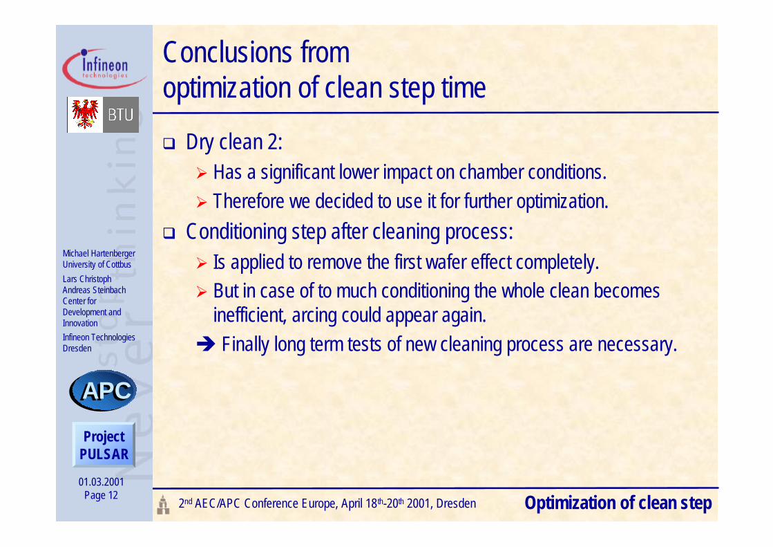
Conclusions fromoptimization of clean step time
q Dry clean 2:Ø Has a significant lower impact on chamber conditions.Ø Therefore we decided to use it for further optimization.
q Conditioning step after cleaning process:Ø Is applied to remove the first wafer effect completely.Ø But in case of to much conditioning the whole clean becomes
inefficient, arcing could appear again.è Finally long term tests of new cleaning process are necessary.
Optimization of clean step

01.03.2001Page 13
Michael HartenbergerUniversity of Cottbus
Lars ChristophAndreas SteinbachCenter forDevelopment andInnovation
Infineon TechnologiesDresden
ProjectPULSAR
APCAPC
2nd AEC/APC Conference Europe, April 18th-20th 2001, Dresden
top-CD vs. time [mean]
17:45 18:14 18:43 19:12 19:40 20:09 20:38 21:07
time
top-
CD
electron collision rate vs. time [median]
3.00E+07
3.50E+07
4.00E+07
4.50E+07
5.00E+07
5.50E+07
6.00E+07
17:45 18:57 20:09 21:21
time
med
ian
ele
ctro
n
colli
sio
n r
ate
[s-1
]
2.30E+07
2.70E+07
3.10E+07
3.50E+07
3.90E+07
Application and optimization of conditioning step
§ Squares in diagrams represent first product wafer after each dry clean
q Electron collision rate indicates first wafer effect on product wafersq Electron collision rate also indicates drift of chamber conditions
(decline of average represented by falling line in diagram)q First wafer effect is also indicated by critical dimensions, measured
on product wafers
Clean
One point – one waferOne point – one wafer
Product
Optimization of conditioning step
01.03.2001Page 14
Michael HartenbergerUniversity of Cottbus
Lars ChristophAndreas SteinbachCenter forDevelopment andInnovation
Infineon TechnologiesDresden
ProjectPULSAR
APCAPC
2nd AEC/APC Conference Europe, April 18th-20th 2001, Dresden
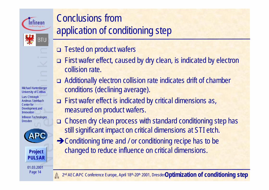
Conclusions fromapplication of conditioning step
q Tested on product wafersq First wafer effect, caused by dry clean, is indicated by electron
collision rate.q Additionally electron collision rate indicates drift of chamber
conditions (declining average).q First wafer effect is indicated by critical dimensions as,
measured on product wafers.q Chosen dry clean process with standard conditioning step has
still significant impact on critical dimensions at STI etch.èConditioning time and / or conditioning recipe has to be
changed to reduce influence on critical dimensions.
Optimization of conditioning step

01.03.2001Page 15
Michael HartenbergerUniversity of Cottbus
Lars ChristophAndreas SteinbachCenter forDevelopment andInnovation
Infineon TechnologiesDresden
ProjectPULSAR
APCAPC
2nd AEC/APC Conference Europe, April 18th-20th 2001, Dresden
electron collision rate vs. time [median]
2.80E+07
3.00E+07
3.20E+07
3.40E+07
3.60E+07
3.80E+07
14:52 15:21 15:50 16:19 16:48 17:16 17:45 18:14 18:43 19:12
time
med
ian
ele
ctro
n
colli
sio
n r
ate
[s-1
]
Modified conditioning step recipe
§ Squares in diagrams represent first product wafer after each dry clean
q Now conditioning step has no CF4/O2, but clean-step is still with CF4/O2
è No significant first wafer effect after each dry cleanØ Now dry clean does not seem to have a big influence on critical dimensions &
electron collision rate
q But: is dry clean still as effective?Ø (Polymers are generated in the conditioning step and without CF4 / O2 even moreè possibly the clean effect is spoiled by the following conditioning step ?)
DRAM product
Optimization of conditioning step
top-CD vs. time [mean]
14:52 15:21 15:50 16:19 16:48 17:16 17:45 18:14 18:43 19:12
time
top
-CD
[n
m]
One point – one waferOne point – one wafer

01.03.2001Page 16
Michael HartenbergerUniversity of Cottbus
Lars ChristophAndreas SteinbachCenter forDevelopment andInnovation
Infineon TechnologiesDresden
ProjectPULSAR
APCAPC
2nd AEC/APC Conference Europe, April 18th-20th 2001, Dresden
electrondensity vs. time [median]
3.00E+08
3.40E+08
3.80E+08
4.20E+08
4.60E+08
5.00E+08
14:24 14:52 15:21 15:50 16:19 16:48 17:16
time
med
ian
ele
ctro
n
den
sity
[cm
-3]
1.80E+09
1.84E+09
1.88E+09
1.92E+09
1.96E+09
2.00E+09
electron density vs. time [median]
3.00E+08
3.40E+08
3.80E+08
4.20E+08
4.60E+08
5.00E+08
14:24 14:52 15:21 15:50 16:19 16:48 17:16
time
med
ian
ele
ctro
n
den
sity
[cm
-3]
1.80E+09
1.84E+09
1.88E+09
1.92E+09
1.96E+09
2.00E+09
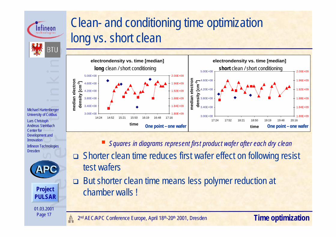
Clean- and conditioning time optimizationlong vs. short conditioning
§ Squares in diagrams represent first product wafer after each dry clean
q Optimization from economic point of view: Influence ofcleaning- and conditioning time on chamber conditions
q Longer conditioning time does not seem to cause changes intrend of electron density for following resist wafers here
long clean / long conditioning long clean / short conditioning
One point – one waferOne point – one wafer
Time optimization
01.03.2001Page 17
Michael HartenbergerUniversity of Cottbus
Lars ChristophAndreas SteinbachCenter forDevelopment andInnovation
Infineon TechnologiesDresden
ProjectPULSAR
APCAPC
2nd AEC/APC Conference Europe, April 18th-20th 2001, Dresden
electrondensity vs. time [median]
3.00E+08
3.40E+08
3.80E+08
4.20E+08
4.60E+08
5.00E+08
17:24 17:52 18:21 18:50 19:19 19:48 20:16
time
med
ian
ele
ctro
n
den
sity
[cm
-3]
1.80E+09
1.84E+09
1.88E+09
1.92E+09
1.96E+09
2.00E+09
electrondensity vs. time [median]
3.00E+08
3.40E+08
3.80E+08
4.20E+08
4.60E+08
5.00E+08
14:24 14:52 15:21 15:50 16:19 16:48 17:16
time
med
ian
ele
ctro
n
den
sity
[cm
-3]
1.80E+09
1.84E+09
1.88E+09
1.92E+09
1.96E+09
2.00E+09
Clean- and conditioning time optimizationlong vs. short clean
§ Squares in diagrams represent first product wafer after each dry clean
q Shorter clean time reduces first wafer effect on following resisttest wafers
q But shorter clean time means less polymer reduction atchamber walls !
long clean / short conditioning short clean / short conditioning
One point – one waferOne point – one wafer
Time optimization

01.03.2001Page 18
Michael HartenbergerUniversity of Cottbus
Lars ChristophAndreas SteinbachCenter forDevelopment andInnovation
Infineon TechnologiesDresden
ProjectPULSAR
APCAPC
2nd AEC/APC Conference Europe, April 18th-20th 2001, Dresden
Long term evaluation of dry clean
q Long term evaluation of new dry clean in normal productionshows no significant influence of dry clean on electroncollision rate of DRAM- product wafers
q Only normal scattering (maybe because of pre- processtolerances) in electron collision rate
Long term evaluation
1.00E+07
1.50E+07
2.00E+07
2.50E+07
3.00E+07
3.50E+07
4.00E+07
4.50E+07
5.00E+07
19.12.00 19.12.00 19.12.00 20.12.00 20.12.00
Med
ian
Ele
ctro
n C
olli
sio
n
Rat
e [s
-1]
21.12.00 21.12.00 21.12.000.00E+00
2.00E+06
4.00E+06
6.00E+06
8.00E+06
1.00E+07
1.20E+07
1.40E+07
1.60E+07
1.80E+07
2.00E+07
Date One point – one wafer
DRAM product
Dry clean
Electron Collision Rate [Median] vs. Date (IT-Mask-Step)
01.03.2001Page 19
Michael HartenbergerUniversity of Cottbus
Lars ChristophAndreas SteinbachCenter forDevelopment andInnovation
Infineon TechnologiesDresden
ProjectPULSAR
APCAPC
2nd AEC/APC Conference Europe, April 18th-20th 2001, Dresden
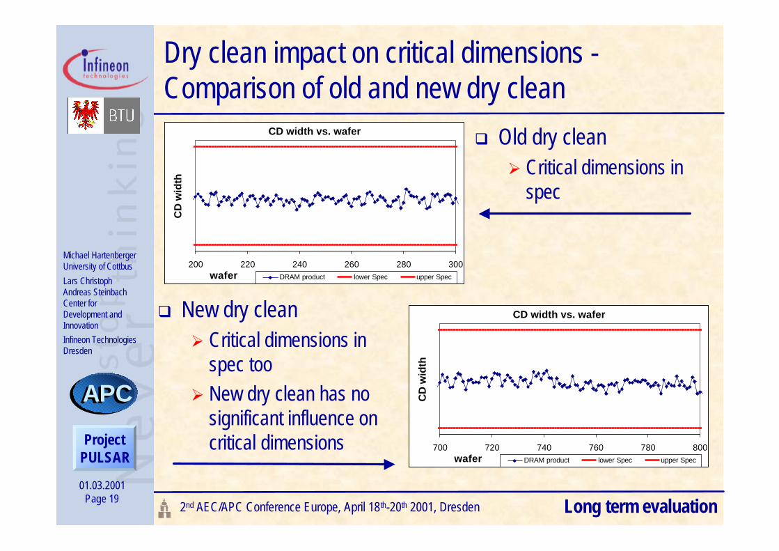
Dry clean impact on critical dimensions -Comparison of old and new dry clean
q New dry cleanØ Critical dimensions in
spec tooØ New dry clean has no
significant influence oncritical dimensions
q Old dry cleanØ Critical dimensions in
spec
Long term evaluation
CD width vs. wafer
200 220 240 260 280 300wafer
CD
wid
th
DRAM product lower Spec upper Spec
CD width vs. wafer
700 720 740 760 780 800wafer
CD
wid
th
DRAM product lower Spec upper Spec
01.03.2001Page 20
Michael HartenbergerUniversity of Cottbus
Lars ChristophAndreas SteinbachCenter forDevelopment andInnovation
Infineon TechnologiesDresden
ProjectPULSAR
APCAPC
2nd AEC/APC Conference Europe, April 18th-20th 2001, Dresden
Summary I: Benefit of plasma parameters
q Electron collision rate and electron density have been used tooptimize a new clean recipe at Shallow Trench Isolation etch inAMAT MxP chamber.
q Both plasma parameters show in real timeØ Dry clean impact on chamber conditions and first wafer effect on
product wafersØ And superimposed long term drift effects of chamber conditions
q Because plasma parameters do indicate chamber conditiondrifts, they can be used to monitor cleaning efficiency withrespect to wall polymers.
q Therefore plasma parameter measurements can significantlyhelp to improve efficiency & reduce costs of dry clean processdevelopment.
Summary

01.03.2001Page 21
Michael HartenbergerUniversity of Cottbus
Lars ChristophAndreas SteinbachCenter forDevelopment andInnovation
Infineon TechnologiesDresden
ProjectPULSAR
APCAPC
2nd AEC/APC Conference Europe, April 18th-20th 2001, Dresden
Summary II: Dry clean optimization
q Benefits of new dry clean:Ø Has no significant impact on critical dimensions of following
product wafers (as shown in short- and long- time observations)Ø Is shorter than old dry clean è higher throughputØ Better clean efficiency than old dry clean (as observed during
chamber opening for maintenance purposes)Ø Chamber up time has been extended by longer dry clean period
è All targets of dry clean optimization (maximize polymerreduction from walls and minimize first wafer effect on criticaldimensions) have been reached in short period of time usingin-situ plasma monitoring techniques.
è Risk of arcing reduced.
Summary
![Performance evaluation of alumina trihydrate and silica ... · of SiR and EPDM composites. According to Refat et al. [27], the dry band arcing and erosion of SiR can be suppressed](https://img.dokumen.tips/doc/110x75/5f47362fa2adac699a0e2187/performance-evaluation-of-alumina-trihydrate-and-silica-of-sir-and-epdm-composites.jpg)