Embed Size (px)
Citation preview

Architectural Considerations for Optimizing SSDs
Santa Clara, CA August 2014
1
Michael Abraham ([email protected]) Advanced Engineering Architect Micron Technology, Inc.
Abstract
• NAND Flash continues to shrink and is making the transition to 3D memories.
• What are some of the challenges that SSD designers face?
• This talk focuses on the NAND and other technologies that are bridging these gaps to improve SSD architecture, performance, reliability, and energy.
Santa Clara, CA August 2014
2

The Beginnings of Flash • 1984 – Toshiba announces “Flash” (IEDM) • 1987 – Toshiba announces NAND Flash (IEDM) • 1994 – Compact Flash: Starts with NOR and later moves to
NAND Flash • 1995 – SmartMedia • 1999 – USB Flash Drive • 1999 – Flash-based Solid State Disk
Santa Clara, CA August 2014
3
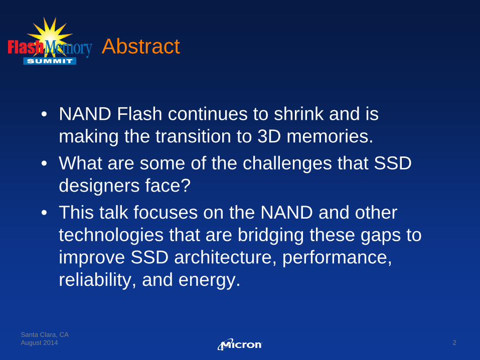
Early Storage Optimizations
Faster Upgradeable
Slightly more expensive
Slow Early obsolescence Relatively inexpensive
Santa Clara, CA August 2014
4
µC NAND
SmartMedia Camera
µC/ SRAM NAND
CF/USB/SD

SSDs: Optimize for Performance
• Fastest use of Flash memory • More expensive ($/bit) than previous solutions
Santa Clara, CA USA August 2014
5
µC NAND Ch0
Ch(n-1)
Power Supplies Host Vcc
DRAM C
O N
N E
C T
O R
…
SATA/SAS/PCIe
SSD Product Priorities
Lower Cost ($/bit) Higher Performance (MB/s, IOPS) Sufficient Reliability (3-5 years) Smaller Form Factors (area/volume) Lower Energy (pJ/bit)
Santa Clara, CA August 2014
6

10
20
30
40Q
4-08
Q1-
09Q
2-09
Q3-
09Q
4-09
Q1-
10Q
2-10
Q3-
10Q
4-10
Q1-
11Q
2-11
Q3-
11Q
4-11
Q1-
12Q
2-12
Q3-
12Q
4-12
Q1-
13Q
2-13
Q3-
13Q
4-13
Q1-
14Q
2-14
Q3-
14Q
4-14
Proc
ess
Nod
e (n
m)
Volume Production Dates
Company A Company B Company C Company D
Lowering SSD Costs: Shrink the NAND
Industry is continuing transition to 3D NAND technologies Santa Clara, CA August 2014
7
Data based on publicly available information
30nm Class
25nm Class 20nm Class 10nm Class
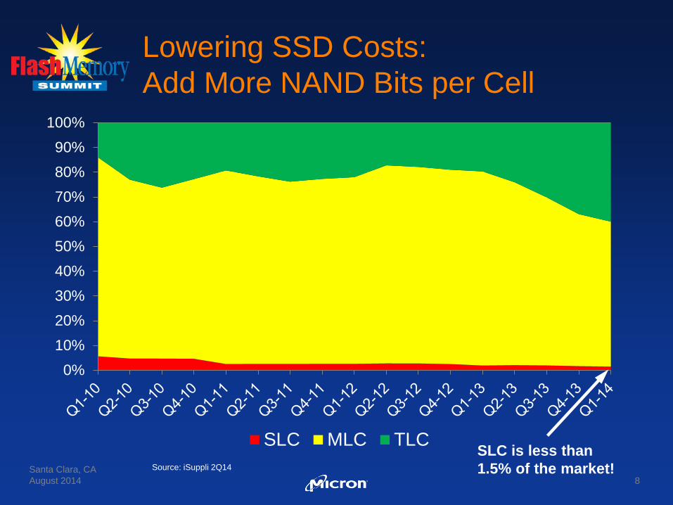
Lowering SSD Costs: Add More NAND Bits per Cell
Santa Clara, CA August 2014
8
0%10%20%30%40%50%60%70%80%90%
100%
SLC MLC TLCSource: iSuppli 2Q14
SLC is less than 1.5% of the market!
Less Expensive SSDs
Mission Accomplished?
Santa Clara, CA August 2014
9
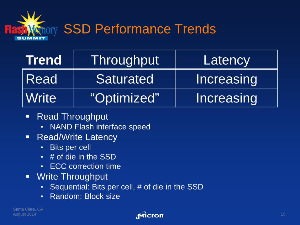
SSD Performance Trends
Santa Clara, CA August 2014
10
Read Throughput • NAND Flash interface speed
Read/Write Latency • Bits per cell • # of die in the SSD • ECC correction time
Write Throughput • Sequential: Bits per cell, # of die in the SSD • Random: Block size
Trend Throughput Latency Read Saturated Increasing Write “Optimized” Increasing
NV-DDR3 NV-SDR NV-DDR
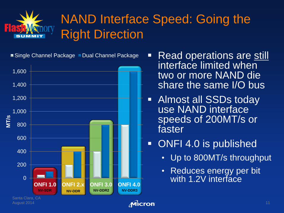
NAND Interface Speed: Going the Right Direction
Read operations are still interface limited when two or more NAND die share the same I/O bus
Almost all SSDs today use NAND interface speeds of 200MT/s or faster
ONFI 4.0 is published • Up to 800MT/s throughput • Reduces energy per bit
with 1.2V interface
Santa Clara, CA August 2014
11
NV-DDR2
0
200
400
600
800
1,000
1,200
1,400
1,600
ONFI 1.0 ONFI 2.x ONFI 3.0 ONFI 4.0
MT/
s
Single Channel Package Dual Channel Package
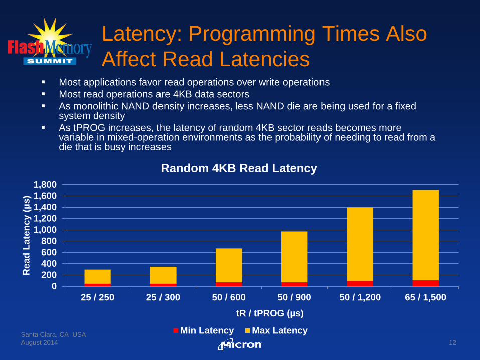
Latency: Programming Times Also Affect Read Latencies
Most applications favor read operations over write operations Most read operations are 4KB data sectors As monolithic NAND density increases, less NAND die are being used for a fixed
system density As tPROG increases, the latency of random 4KB sector reads becomes more
variable in mixed-operation environments as the probability of needing to read from a die that is busy increases
Santa Clara, CA USA August 2014
12
0200400600800
1,0001,2001,4001,6001,800
25 / 250 25 / 300 50 / 600 50 / 900 50 / 1,200 65 / 1,500
Rea
d La
tenc
y (µ
s)
tR / tPROG (µs)
Random 4KB Read Latency
Min Latency Max Latency
0.0
20.0
40.0
60.0
80.0
Data Bytes per Operation (Page Size * # of Planes)
Sequential Programming Throughput (MB/s)
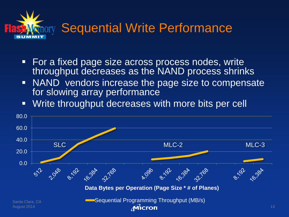
Sequential Write Performance
For a fixed page size across process nodes, write throughput decreases as the NAND process shrinks
NAND vendors increase the page size to compensate for slowing array performance
Write throughput decreases with more bits per cell
Santa Clara, CA August 2014
13
SLC MLC-2 MLC-3
8
32
128
512
2048
8192
32768
131072
524288
2097152
8388608
Block size (B) Data Bytes per Operation Pages per Block
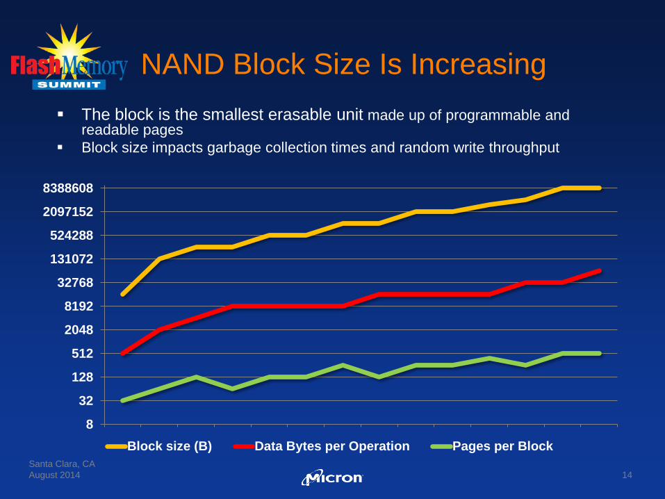
NAND Block Size Is Increasing The block is the smallest erasable unit made up of programmable and
readable pages Block size impacts garbage collection times and random write throughput
Santa Clara, CA August 2014
14

Performance Optimizations
• Overprovision the amount of NAND die (slightly higher cost) • Use smaller NAND die on the latest litho • Use largest NAND die on the latest litho and add a few
• Write data sequentially to the NAND • Improve garbage collection algorithms (e.g.
TRIM) and scheduling
Santa Clara, CA August 2014
15
Node NAND Density Data size # of Die Seq Write (MB/s) Gen 1 32Gb (4GB) 8192 32 230 Gen 2 64Gb (8GB) 16,384 16 184 Gen 3 128Gb (16GB) 32,768 8 133 Gen 3 64Gb (8GB) 32,768 16 324
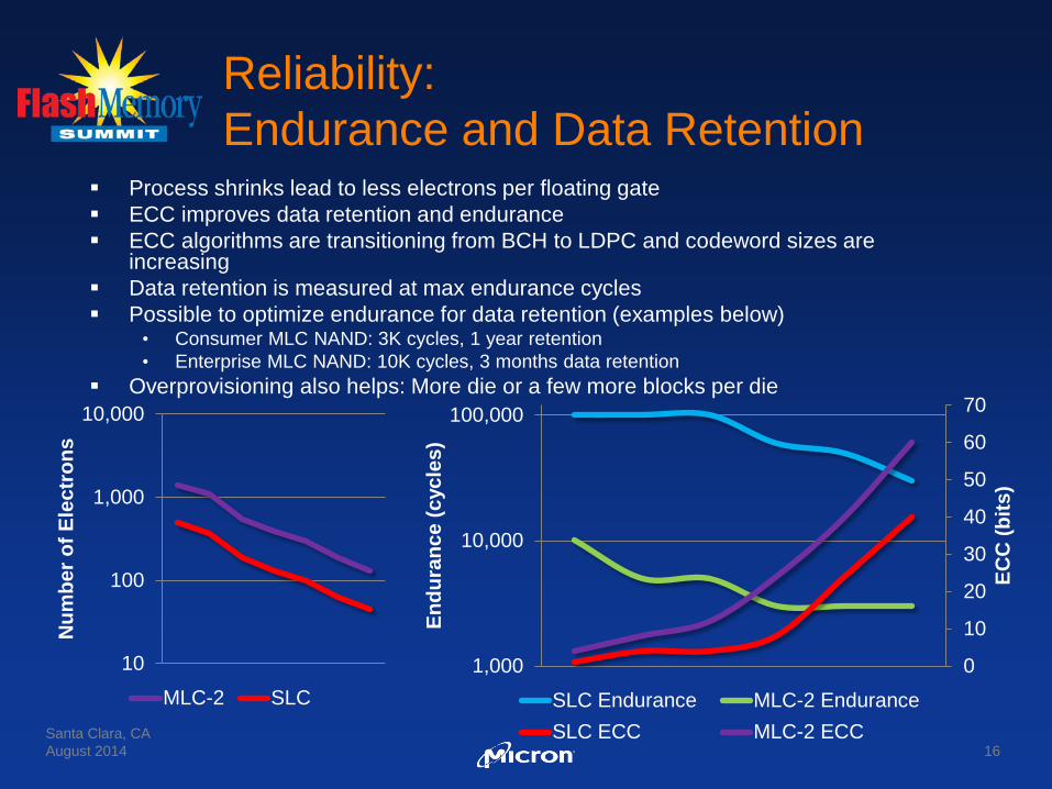
Reliability: Endurance and Data Retention
Santa Clara, CA August 2014
16
Process shrinks lead to less electrons per floating gate ECC improves data retention and endurance ECC algorithms are transitioning from BCH to LDPC and codeword sizes are
increasing Data retention is measured at max endurance cycles Possible to optimize endurance for data retention (examples below)
• Consumer MLC NAND: 3K cycles, 1 year retention • Enterprise MLC NAND: 10K cycles, 3 months data retention
Overprovisioning also helps: More die or a few more blocks per die
10
100
1,000
10,000
Num
ber o
f Ele
ctro
ns
MLC-2 SLC0
10
20
30
40
50
60
70
1,000
10,000
100,000
ECC
(bits
)
Endu
ranc
e (c
ycle
s)
SLC Endurance MLC-2 EnduranceSLC ECC MLC-2 ECC
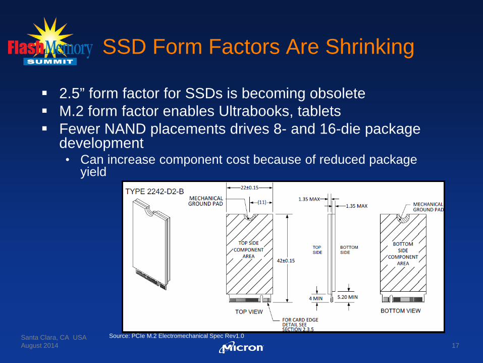
SSD Form Factors Are Shrinking
2.5” form factor for SSDs is becoming obsolete M.2 form factor enables Ultrabooks, tablets Fewer NAND placements drives 8- and 16-die package
development • Can increase component cost because of reduced package
yield
Santa Clara, CA USA August 2014
17
Source: PCIe M.2 Electromechanical Spec Rev1.0

Energy
Energy was previously not a high priority Becoming very important in battery-powered
systems Rule of thumb: “Hurry up and wait” Ways to reduce energy
• Queue and burst operations • Reduce write amplification • Increase interface speed and lower its voltage
Santa Clara, CA USA
August 2014
18
SLC Mode
Some MLC and TLC NAND Flash have the ability to write and read data in SLC mode
Smaller block size; mode is determined block by block and managed by the SSD controller • MLC (X pages per block) SLC Mode (1/2 X) • TLC (Y pages per block) SLC Mode (1/3 Y)
Array times decrease, particularly for tPROG to 300-500µs resulting in higher burst performance
Excellent enabler for TLC-based SSDs for lower SSD costs
Initial write uses less energy as tPROG is shorter Best improvement with bursty workloads (e.g.
consumer applications) Santa Clara, CA USA
August 2014
19
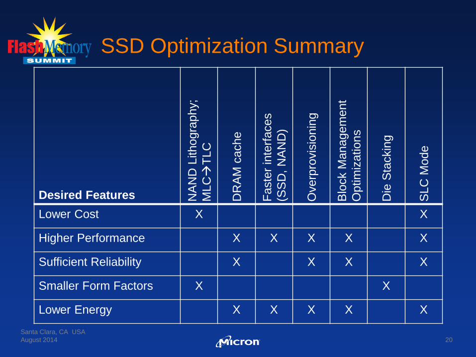
SSD Optimization Summary
Desired Features NA
ND
Lith
ogra
phy;
M
LC
TLC
DR
AM
cac
he
Fast
er in
terfa
ces
(S
SD
, NA
ND
)
Ove
rpro
visi
onin
g
Blo
ck M
anag
emen
t O
ptim
izat
ions
Die
Sta
ckin
g
SLC
Mod
e
Lower Cost X X
Higher Performance X X X X X
Sufficient Reliability X X X X
Smaller Form Factors X X
Lower Energy X X X X X
Santa Clara, CA USA August 2014
20

Questions?
Santa Clara, CA August 2014
21
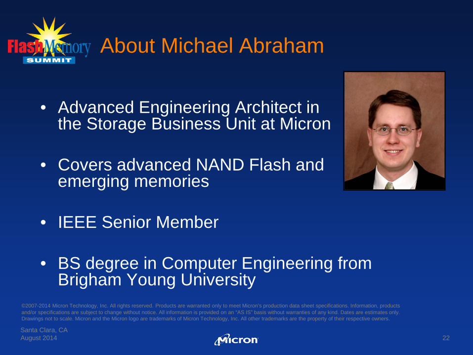
About Michael Abraham
• Advanced Engineering Architect in the Storage Business Unit at Micron
• Covers advanced NAND Flash and emerging memories
• IEEE Senior Member
• BS degree in Computer Engineering from Brigham Young University
Santa Clara, CA August 2014
22
©2007-2014 Micron Technology, Inc. All rights reserved. Products are warranted only to meet Micron’s production data sheet specifications. Information, products and/or specifications are subject to change without notice. All information is provided on an “AS IS” basis without warranties of any kind. Dates are estimates only. Drawings not to scale. Micron and the Micron logo are trademarks of Micron Technology, Inc. All other trademarks are the property of their respective owners.