Embed Size (px)
Citation preview

SLIC DevicesApplications of the SLIC Devices
Introduction to the SLIC Product Family
Application Note
SLIC FAMILY FUNCTIONAL DESCRIPTIONZarlink’s SLIC device family has grown and includesdevice operating characteristics and options not pre-viously available. Current offerings also include newchoices of power management and DC feed control toaddress needs of major telephony markets. Althoughcertain features may be unique to a specific SLIC de-vice type, all Zarlink SLICs are based on and containthe same functional blocks. The following sectionsdescribe, in detail, the operation of each of theseblocks.
Two-Wire InterfaceThe function of the two-wire interface is to provide DCcurrent and to send voice signals to a telephone appa-ratus connected to the linecard with a two-wire line.The two-wire interface also receives the returning voicesignals from the telephone transmitter.The typical two-wire interface (see Figure 1) consists oftwo current mode line-driver amplifiers, line-voltagesensing circuits with AC/DC pass separation, and aloop-current sensing circuit.The current mode amplifiers driving the A(TIP) andB(RING) pins are controlled by two input signals, ILI andIMI. ILI controls the longitudinal (common mode) cur-rent, and IMI controls the metallic (differential) current.The two-wire currents are:
Where: K1 is the internal current mode amplifier gain.
IMI is equal to the current into the Receive SummingNode (RSN), which is the terminating point for the ex-ternal networks controlling two-wire impedance, re-ceive gain, battery feed, and metering gain (in meteringversions). These networks are described in detail later.ILI controls the longitudinal line current to obtain the op-timum common mode DC operating point for the cur-rent mode amplifiers.
The voltage sense signal (VACMET) that goes to the sig-nal transmission block is the AC metallic component ofthe A and B voltages.
Two voltage sense signals (|VDCMET| and VLONG) go tothe power feed controller block. VDCMET is the DC me-tallic component of the A and B voltages. VLONG is thelongitudinal component of the A and B voltages.
An external capacitor (CHP), connected between HPAand HPB, separates the AC and DC components of themetallic voltage. Because the time constant could betoo long during polarity reversal or pulse dialing, thetwo-wire interface can have a shorting circuit that de-creases the time constant during these events.
The loop-current sensing circuit produces a current (ID)that is proportional to the magnitude of the loop currentand is output to the RD pin. An external resistor and filtercapacitor connected to RD converts this current to a fil-tered voltage for use by the off-hook detector.
Note: This describes the two-wire interface for most ofZarlink’s SLIC devices. Minor differences may existon certain device types, but all follow this general for-mat and operation.
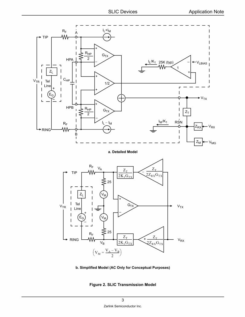
Signal TransmissionFigure 2 provides more detail of the SLIC transmissionpath. This path is split between the signal transmissionblock and the two-wire interface block.
The AC line voltage is sensed by differential amplifiersbetween the A and HPA leads, and between the HPBand B leads. The outputs of these amplifiers are equalto the AC metallic components of the line voltages.These voltages are summed and buffered by the opamp GTX. GTX in dB is specified in each data sheet undertwo- to four-wire gain accuracy. For metering applica-tions, GTX is typically –6.02 dB to avoid overload duringmetering signal transmission. Longitudinal voltages arerejected by the differential amplifiers and only affect VTXto the extent of the longitudinal balance specification.
The balance return signal on VTX exhibits 180° phaseshift with respect to VRX. This allows the two-wire ACinput impedance to be programmed by means of an ex-ternal impedance that is connected between RSN andVTX (see Figure 2). This impedance may be a complexR-C network and should be K1 times the desiredtwo-wire input impedance minus K1 times the fuse re-sistors. This means resistors become K1 times largerand capacitors become K1 times smaller. Note that anyexternal stray capacitance between VTX and RSN mustbe included in ZT when precise computations for outputimpedance, gain, transhybrid loss, or return loss arebeing made.
Where: Z2WIN = desired two-wire impedance
IAX K1 ILI IMI+( ) and IBX K1 ILI IMI–( )==
ZT K1 G• TX Z2WIN 2RF–( )=
Document ID# 080284 Date: Oct 10, 2007Rev: B Version: 2Distribution: Public Document

SLIC Devices Application Note
The four-wire output is found on the VTX terminal, andthe four-wire input terminal is VRX (see Figure 2b). Bothof these ports are referenced to analog ground (AGND).
Because the fuse resistors are outside the feedbackloops, they influence the effective gains. These gainsare as follows:
CurrentSensing
CurrentSensing
+
+ Σ
+
+
Protection
Protection
BGND
VREGVREG
RF
VREG
IMI
ILI
VDCMET
VLONG
GTX
1/2
1
GTXShorting Circuit
RHP
2
CHP
HPB
HPA
Shorting Circuit
RF
VREG
IL − IMK1
K1
B Current Amplifier
A Current Amplifier
RING
TIPIL + IM
VACMET
RLOOP
ILOOP = IM
IM = IMI • K1
+
+
+
+
Figure 1. Two-Wire Interface (Typical)
|ISENSE A|
|ISENSE B|
A(TIP)
B(RING)
IL = ILI • K1
Σ
+
–
ILI
IMI
+
+ID
–
–
–
–
–
–
RHP
2
Absolute Value
ILOOP292
------------------
RS/2
RS/2
Absolute Value
Absolute Value
G42LVAVRX---------- EG 0=[ ]
ZLZRX---------- •
K1ZTZT K1GTX ZL 2RF+( )+----------------------------------------------------------–==
G24VTXVA---------- VRX 0=[ ]
ZTK1------
2RFZT
K1GTX-----------------+
----------------------------------==
G44LVTXVRX---------- EG 0=[ ]
ZTZRX----------
ZL 2RF+( )
ZL 2RFZT
K1GTX-----------------+ +
----------------------------------------------–==
2Zarlink Semiconductor Inc.
SLIC Devices Application Note
b. Simplified Model (AC Only for Conceptual Purposes)
HPA
++
–
+
–
+
–
+
+
–+
–
GTX
VM
VTRTel
Line
RF
RF
VTX
VRX
TIP
RING
25
25
VB
GTX
GTX
1/2
1
IL+IM
IL/K1 25K (typ) VLBIAS
VTX
VRX
VMG
IM/K1RF
Tel Line
RF
RHP
2
RHP2
IL − IM
TIP
RING
a. Detailed Model
CHP
Figure 2. SLIC Transmission Model
+
EG
+
–
ZL
EG
ZL
−
ZT
ZRX
ZM
RSN
HPB
VA
VTR
A
B
ZT2K1GTX--------------------
ZT2ZRXGTX------------------------
ZT2K1GTX-------------------- ZT
2ZRXGTX------------------------
VMVA VB–2
--------------------=
VM
3Zarlink Semiconductor Inc.

SLIC Devices Application Note
The dynamic performances of K1 (the current amplifiergain) and GTX (the transmit voltage amplifier gain) aremodeled by the following S-domain transfer functions:
Where: K1 = Current amplifier DC gain ZAB = Load between the A and B pins GTX = Two- to four-wire transmit path
midband gainRHP = Internal resistance, typically 424KRS = Current sensing resistance
These functions are useful for the prediction of sys-tem return loss and echo cancellation performance.The value of K1 can be found in each device’s datasheet referred to as the current gain. GTX in dB isspecified in each data sheet under two- to four-wiregain accuracy. CHP sets the low frequency limit of thevoice band response.
The transmission circuit also contains a longitudinalfeedback circuit to shunt longitudinal signals to a DCbias voltage (VLBIAS) which comes from the power feedcontroller. Longitudinally, the SLIC devices typically ap-pear as 25 Ω resistors from A and B to VLBIAS. The lon-gitudinal feedback does not affect metallic signals.
In metering versions, metering signals are injected byadding an additional current into summing point RSNthrough an external impedance, ZM.
Power Feed ControllerThe power feed controller has three sections: (1) thebattery feed circuit; (2) the polarity reversal circuit; and(3) the bias circuit. These are shown in Figure 3.
The battery feed circuit regulates the amount of DC cur-rent and voltage supplied to the telephone over a widerange of loop resistance. The polarity reversal circuitprovides the capability to reverse the loop current forpay telephone keypad disable and other applications.The bias circuit provides a reference voltage, which isoffset from the subscriber line voltage. The referencevoltage can control the switched mode regulator(switching regulator versions only, described later),which minimizes SLIC power consumption by providingthe minimum supply voltage needed by the line driversfor proper operation. The reference voltage also cancontrol the switching point for automatic battery switch-ing SLIC devices.
VDCMET is the DC component of the voltage between Aand B. When CHP is 0.33 µF, the low-pass filter formed
by RHP and CHP attenuates frequencies above 1.2 Hz.The loop current is equal to K1 times the current intothe Receive Summing Node (RSN), which is equal tothe voltage on RDC divided by RDC1 + RDC2. The val-ues of the programming resistors, RDC1 and RDC2,should be kept somewhat equal in order to minimizethe size of CDC.
In constant current feed versions, the battery feed cir-cuit produces a voltage at the RDC pin whose magni-tude is equal to 2.5 V, and whose sign depends on thefeed polarity desired (negative for normal polarity andpositive for reverse polarity). The net result is a con-stant current feed with the feed current given by the fol-lowing equation:
For example, if K1 is 1000 and a loop current of 40 mAis desired:
In this example, values of RDC1 and RDC2 of 31.25Kcould be used.
For resistance feed versions, the battery feed producesa voltage at the RDC pin whose magnitude is equal to(50 – |VDCMET|)/20, and whose sign depends on thefeed polarity desired (negative for normal polarity andpositive for reverse polarity). The net result is an appar-ent open circuit voltage of 50 V and a feed resistance,RFEED, equal to 20(RDC1 + RDC2)/K1; thus, the feed re-sistance is programmable, but the apparent open cir-cuit voltage is not. Including the fuse resistors RF, thetotal feed resistance is then:
For example, if K1 = 1000, and a feed resistance of840 Ω is desired using 20 Ω fuse resistors:
In this example, values of RDC1 and RDC2 of 20K couldbe used.
All SLIC devices have an anti-saturation guard thatprevents the output amplifiers from saturating underlong loop high resistance conditions, which maintainsAC transmission by preventing clipping. Some of theSLIC devices implement multiple anti-saturation re-gions that may track the battery voltage or may operateat pre-determined fixed thresholds. Battery-indepen-dent anti-saturation noise performance is normallyidentical to that of normal loop feed, however, on somedevices, anti-saturation that tracks the battery voltagemay provide an additional path for battery-referencednoise entering the transmission path.
K1 S( ) K11
1 1.15 10 8– RS ZAB S( )+[ ] S•••+---------------------------------------------------------------------------------------=
GTX S( )GTX
1 1RHP CHP S---------------------------+
------------------------------------ 1
1 4.5 10 7– S•+------------------------------------•=
IFEED2.5K1
RDC1 RDC2+--------------------------------=
RDC1 RDC2 2.5 1000•40
------------------------- 62.5K= =+
RFEED 2RF20 RDC1 RDC2+( )
K1-------------------------------------------+=
RDC1 RDC21000 840 2 20•–( )
20------------------------------------------------ 40K= =+
4Zarlink Semiconductor Inc.

SLIC Devices Application Note
As an example, most switching regulator SLICs havetwo anti-saturation regions. In these SLICs, when theVAX to VBX voltage reaches a threshold of approxi-mately 30 V (exact voltage depends on SLIC version),the Anti-sat 1 region of operation is entered. In this re-gion, the feed synthesis loop gain is greatly increased,thereby reducing the output resistance to a much lowervalue. The output voltage then rises at a slower ratewith increasing loop resistance, thereby keeping theamplifier out of saturation. All transmission specifica-tions are met in the Anti-sat 1 region.
If the line voltage increases further to greater than ap-proximately 5 to 15 V (exact voltage depends on SLICversion) below VBAT, the SLIC goes into the Anti-sat 2region where the loop gain is further increased and theoutput resistance decreased. In this region, the voltagerises very slowly, with increasing loop resistance, andthe DC feed of the SLIC looks almost like a constantvoltage source. The transmission specifications in theAnti-sat 2 region may be somewhat degraded.
Some of the SLIC devices implement a battery-depen-dent anti-sat scheme, where a pin (CAS pin) on theSLIC is provided to filter noise that may originate fromthe battery source. The size of the CCAS capacitor con-nected to the CAS pin affects the amount of filtering,and therefore affects VBAT PSRR performance. Loadlines and equations describing all regions of operationare provided in each device data sheet.
To obtain polarity reversal, the input decoder and con-trol circuit send a signal that reverses the sign of thevoltage on the RDC pin. During reversal, sense resis-tors RHP are shunted to reduce the time constantformed by RHP and CHP. This allows the polarity rever-sal time to be controlled only by CDC and its parallelcombination of RDC1 and RDC2. A typical polarity transi-tion time is 1.5 ms. In the previous example for a resis-tance feed version SLIC, RDC1 and RDC2 werecomputed to be 20K. The value of CDC should then be0.15 µF.
The longitudinal control loop operates by deriving aninternal reference voltage VLBIAS. This voltage is givenby:
The additional BIAS is added to provide enough “head-room” for the amplifiers to always operate in the linearregion. The value of BIAS varies depending on theSLIC type. Any longitudinal voltages appearing on theline are shunted to VLBIAS via a 25 Ω resistance. Nor-mal transmission performance is maintained providedthe resulting current is less than the specified longitudi-nal current capability. The VREF output is fed to theswitching regulator (switching regulator SLICs only),which adjusts VREG, the voltage supplying the line out-
put amplifiers, until (for most devices) it is equal totwice VLBIAS.
Power ManagementThe operation of the power-feed controller in mostZarlink SLIC devices results in the A pin maintaininga fairly constant voltage below Battery Ground, whilethe voltage on the B pin varies depending on the DC re-sistance of the loop. This means that as the loop lengthdecreases, the voltage dropped across the B currentamplifier and the corresponding power dissipation in-creases. Zarlink has implemented a number of tech-niques to take advantage of this characteristic tominimize the on-chip and in some cases, total systempower dissipation.
Switching RegulatorThe first technique is to implement a switching regula-tor function on-chip with a few external components(see Figure 4). The power-feed controller generates areference voltage VREF, which is the minimum voltagerequired to feed the output line amplifiers and is equalto twice VLBIAS. The switching regulator adjusts VREG,the operating voltage for the output amplifiers, to equalVREF. The efficiency of the switching regulator (>80%)minimizes both the on-chip power dissipation and thesystem power dissipation. This is particularly importantfor short loops operating at high currents, which other-wise cause high power dissipation.
A 250 to 300 kHz clock is required at input CHCLK tooperate the switching regulator. The switch control tellsthe switch to disconnect the L pin from VBAT at the be-ginning of each CHCLK cycle, and connect it for a timethat depends upon the difference between VREF andVREG. During this time, the current through the inductordecreases. A comparator senses when VREG fallsbelow VREF and the inductor is again switched to VBAT.The result is that the average value of VREG is alwaysheld equal to the value of VREF. The filter capacitor,CFIL, between VREG and BGND smooths out the ripplecaused by the inductor switching action.
The regulator is a high-gain feedback circuit, and there-fore requires the stabilization network formed by RCH,CCH1, and CCH2 between VREG and CHS.
The design and layout of the external switching regula-tor circuitry is very important. Fast switching currentscan occur in the catch diode, D1, and in the VBAT filtercapacitor, CBAT. These must be low inductance compo-nents with short leads. Capacitor CFIL must have loweffective series resistance at high frequencies. A sta-ble, voltage-insensitive capacitor, such as a metallizedpolyester type, should be used.
The connections from the diode to the L pin, from CBATto the VBAT pin, and from the diode to CBAT must all beshort, low-inductance connections. The L pin is subjectto very fast voltage transients as the switch turns on
VLBIASVDCMET BIAS+( )–
2-----------------------------------------------------------=
5Zarlink Semiconductor Inc.

SLIC Devices Application Note
and off, so all of the connections to this pin must be iso-lated from sensitive signals by means of traces con-nected to BGND. All of the external components in theregulator circuit must have voltage ratings in excess ofthe maximum battery voltage. In addition, the diodemust have a reverse recovery time of less than 4 ns. All
the switching-regulator SLIC devices in a systemshould be synchronized to a common clock to preventintermodulation products and crosstalk in the voiceband. For systems that include coding, the clockshould be synchronous to the sampling frequency.
RDC1 RDC2+K1
--------------------------------
+
–
Absolute Value
+
–
Anti-saturation Guard
Tel Line
VREG
BGND
IL + IM
+1 = Normal–1 = Reverse
VREF
VLBIAS1/2
–1
1/201
IL − IM VREG
BGND
Note
BIAS
RHP2
RHP2
CHP
Tel Line
TIP
RINGRF
RL
RDC2
CDC
RDC1RDC
RFVBAT
IMI = IM/K1
RF
RF
RL
B
ANormal
See Feed Options at
Right
25
25
+
–
VAX – VBX
Current Feed Option
Resistance Feed Option
50 V
Longitudinal
BIAS/2
a. Detailed Model
b. Simplified Model
–2.5 V
Note:The 1/20 operational amplifier is only present in constant resistance feed versions of the SLIC.
HPB
HPA
Figure 3. SLIC Power Feed Controller
RSN
2.5K1RDC1 RDC2+--------------------------------
20
A
B
K1
TIP
RINGReverse
6Zarlink Semiconductor Inc.

SLIC Devices Application Note
Thermal ManagementThis power management technique offloads thermalenergy from the SLIC to an external resistor, RTMG. Thecircuit configuration is shown in Figure 5. An externalresistor is used to share some of the loop current withthe B-leg current amplifier, especially on short lines.This limits the on-chip power dissipation and allows alow cost plastic package to be used while reducing ex-ternal component count compared to the switching reg-ulator solution. The RTMG resistor is normally selectedso that with the programmed loop current being fed intoa short circuit loop from the nominal battery, all of theloop current is supplied by RTMG. Equations to calcu-
late this resistance and the resulting power dissipationin the SLIC and RTMG are provided in the individualdata sheets.
This feature operates in Normal and Reverse PolarityFeeding states for most SLIC devices. However, someSLIC devices only support thermal management in theNormal Polarity state. Refer to the specific data sheets.
BGND VREG
QBATVREF (Power Feed Controller)
CHCLK
CHSQBATVBAT
CQ
D6
CCH1RCH
CFIL
CBAT
VREGDI
L
VBAT
CCH2
BGND
Figure 4. SLIC Switching Regulator
Switch Control
L
(250–300 kHz)
7Zarlink Semiconductor Inc.

SLIC Devices Application Note
Battery SwitchingThe third power management technique is batteryswitching operation. This technique allows both the de-vice and system power dissipation to be minimized.
This solution provides for high on-hook voltage acrossthe line, for on-hook recognition or to ensure operationwith MTU’s, while allowing low off-hook power dissipa-tion by switching to a lower battery voltage.
Input Decoder and ControlThe input decoder and control block provides a meansfor a microprocessor or SLAC™ IC to control suchsystem functions as line activate, OHT, ringing, andpolarity reversal.
The input decoder and control block has TTL-compatible inputs, which set the operating states of theSLIC. C3–C1 inputs are common to most versions andcan select up to eight operating states. Other inputs areavailable for relay drivers as provided by certain SLICs.
E0 and E1 control the function of the DET output. 1summarizes the available SLIC operating states formost devices.
Up to three detectors are implemented on-chip to sup-port the necessary signaling functions. The status ofthese detectors is reported through a single output,DET. Three control signals determine what informationis provided at this output.
A signal from the state decoder selects between thering trip comparator and loop detect/ground key (see1). The E1 input selects between loop and ground key.Finally, the active high E0 input (when the SLIC is soequipped) enables the DET output, which is an opencollector with an internal pull-up. The individual devicedata sheets should be used to determine which controllines are available with a given device/package optionand to determine the polarity of E1.
A(TIP)
B(RING)
RLOOP
BGND
ILOOP
ISLIC
ITMG
TMGVBAT
RTMG
Battery
ThermalManagement
SLIC
Notes:1. A(TIP) lead remains at a relatively constant voltage (a few volts below ground) while B(RING) lead becomes more negative
as loop resistance increases.2. External resistor (RTMG) shares loop current (ILOOP) with SLIC.
3. Internal circuit and RTMG resistor choice ensures maximum loop current is fed through RTMG at shortest loop conditions.
4. The TMG connection is inside the SLIC’s current sense loop, so as more current to the loop is provided through TMG, thecurrent from the B lead amplifier is reduced, as is the SLIC’s power dissipation.
5. The diagram shows scheme functionality. Fault control and other function switching are not shown.
Figure 5. Simplified SLIC Thermal Management
8Zarlink Semiconductor Inc.

SLIC Devices Application Note
Notes:Open Circuit: When the SLIC is in the Open Circuit state, both the A(TIP) and B(RING) power amplifiers are switched off and present high impedance to the line. The Open Circuit state has the lowest power dissipation. Loop detectors are inoperative in this state. This function is useful for allowing line-powered relays to collapse, denying power to out-of-service lines, as well as allowing clearing of line faults.Ringing: When the SLIC is in the Ringing state, the ring relay driver (RINGOUT) is activated, and the ring-trip detector is readable at DET. Also, the A(TIP) and B(RING) are both open circuits. While the SLIC is in the Ringing state, signal transmission is inhibited.Active: In states where normal, Active operation is indicated, the standard battery convention applies; A(TIP) is near ground and sources current. B(RING) is near VBAT and sinks current. During Active state operation, all signal transmission and loop super-vision functions operate, and the off-hook detector or ground-key detector is gated to DET.OHT: The OHT (On-Hook Transmission) operating state is the SLIC’s low-power mode in which the battery feed circuit limits the DC loop current to typically 0.5 (value depends on SLIC version) times the Active state short circuit current limit. In this state, the off-hook detector works normally, and all signal transmission functions operate normally. Previously, this OHT state was desig-nated the Disable state in earlier Zarlink SLIC documentation.Tip Open: When the SLIC is in the Tip Open state, the A(TIP) power amplifier is switched off so that it presents a high impedance to the line. This mode is provided to facilitate ground-start signaling.Standby: The Standby state (on SLICs so equipped; see specific data sheets) is used for supervision purposes only. The A and B amplifiers are completely turned off (similar to the Open Circuit state) and DC feed through the loop is provided by an internal resistive feed network. Loop detect functions operate normally, but signal transmission is not enabled. This allows for monitoring off-hook transitions while maintaining lowest possible power consumption.Active Polarity Reversal: When the SLIC is in Active Polarity Reversal state, the normal battery feed convention is reversed, with B(RING) approaching ground and sourcing current, while A(TIP) approaches battery and sinks current. While A(TIP) and B(RING) are in transition, the off-hook function is meaningless because the loop current must pass through zero.OHT Polarity Reversal: This state is similar to the OHT state, except that the DC feed polarity is reversed.* With no DC loading, on-hook condition
Table 1. SLIC Decoding and State Description (most devices)
Amplifier Output * DET Output
State Two-Wire State A(TIP) B(RING) E1/E1See SLIC Data Sheet
Ring Relay Active
0 Open Circuit High-Z High-Z Ring trip Ring trip No
1 Ringing High-Z High-Z Ring trip Ring trip Yes
2 Active Near BGND Near VBAT Loop detector Ground key No
3 OHT (On-Hook TX) Near BGND Near VBAT Loop detector Ground key No
4 Tip Open High-Z Near VBAT Loop detector — No
5 Standby Near BGND Near VBAT Loop detector — No
6 Active Polarity Reversal Near VBAT Near BGND Loop detector Ground key No
7 OHT Polarity Reversal Near VBAT Near BGND Loop detector Ground key No
9Zarlink Semiconductor Inc.

SLIC Devices Application Note
Off-Hook DetectorThe first and most important loop monitoring function,provided on all SLIC devices, is off-hook detection. Theblock diagram of this detector is shown in Figure 6.
The two-wire interface produces a current equal inmagnitude to the loop current divided by KS, and sendsit out on the RD pin. An external resistor and capacitor(RD and CD) connects the RD pin to the detector refer-ence. The value of the voltage across resistor RD is thecurrent leaving the RD pin times the value of RD. Theoff-hook detector outputs a logic Low when this voltagerises above a threshold voltage of typically 1.25 V.
The value of RD required for a desired off-hook line cur-rent threshold is then (see SLIC data sheet for propernumerator value):
where KS = 292 and VT = 1.25 V
The value of Cd for a typical on-hook to off-hook timeconstant of 0.5 ms should satisfy the following relation:
RDKS VT•
ITHRESH--------------------=
RDCD 0.5 ms=
MUX
VCC
C1
DET
E0
E1
+
+ –VT
Detector Reference(VEE or GND)*
RD CD
Two-Wire Interface
Comparator
RD
A(TIP)
B(RING)
ILOOP
ILOOP
Input Decoder and Control
InputDecoder
Figure 6. Signaling Off-Hook Detection
–
* See SLIC data sheet
ILOOPKS--------------
C2C3
SHD
GKD
RTD
10Zarlink Semiconductor Inc.

SLIC Devices Application Note
Ground-Key DetectorThe Ground-Key Detector (see Figure 7) compares thelongitudinal control current (ILI) to an internally gener-ated threshold current, ILT. The current flowing in theearth loop is proportional to the longitudinal control cur-rent. When the current in the earth loop exceeds thethreshold value, the ground-key signal forces the DEToutput Low when selected by E1.
On some SLIC versions, a ground key filter pin is pro-vided. This allows attenuation of AC longitudinal cur-rents and produces a more reliable detect output. Theminimum GKFIL capacitor is 3.3 nF. It forms a low-passtransfer function with an on-chip 36 kΩ resistor. Largercapacitance values can be used to achieve the desiredAC rejection.
InputDecoder
MUX
VCC
C1
DET
–ILT
ILI
C2C3
E0E1
Figure 7. Ground-Key Detector
GKFIL
36 kΩ
Input Decoder and Control
SHD
GKD
RTD
11Zarlink Semiconductor Inc.

SLIC Devices Application Note
Ringing CircuitA generalized ringing circuit is shown in Figure 8. Incommon applications, the circuit can be simplified asshown later. During ringing, the ring relay driver is acti-vated and the A(TIP) and B(RING) leads are placed inthe Open Circuit state. The ring feed source is con-nected by the ring relay to the line through ring feed re-sistors R1 and R2.
When an off-hook condition occurs, the bridging resis-tors RB1, RB2, R3, and R4, and filter capacitors CRT1 andCRT2 cause the voltage on DB to go positive with re-spect to DA and the detector (DET) output goes Low.
If RLMAX is the maximum line resistance that is to be de-tected as an off-hook, the bridging resistors should bechosen such that:
Where:
The capacitors reduce the effective amplitude of theringing signal by a factor of 1/ 1+j2πfrt.
Where:
For fr = 20 Hz ringing, CRT should be chosen to give avalue of t = 50 ms. This reduces the ringing by a factorof 6.4 and allow detection within two ringing cycles.
For balanced ringing, the ringing voltage splits betweenthe ground and battery sides. The resistors should bebalanced, (i.e., R1 = R2, RB1 = RB2, and R3 = R4). A sin-gle capacitor of half the value between DA and DB canreplace the capacitors CRT1 and CRT2.
For unbalanced ringing on the ground side, useequal networks with R1 = R2, RB1 = RB2, R3 = R4, andCRT1 = CRT2.
For unbalanced ringing on the battery side, the follow-ing simplification can be made. The positive side of theringing supply is grounded and R1 is replaced by ashort circuit. In this case, the R4, RB2, and CRT2 net-work can be combined with other channels into a ringerthreshold because the voltage on the DA pin is inde-pendent of line conditions.
RB1R3---------
RB2R4--------- RLMAX RFEED+( )
RLMAX R1+( )--------------------------------------------==
RFEED R1 R2+=
tR3RB1CRT1R3 RB1+----------------------------
R4RB2CRT2R4 RB2+----------------------------+=
InputDecoder
MUX
VCC
DET
E0
E1
Input Decoder and Control
Comparator
Ring Relay Driver
KR
A
B
DA
DB
RB1
RB2
R3
R4
RF
RF
R2 R1
Ringing Source
Tel Line
TIP
RING
+
KR
KR
Ring Relay
CRT2 CRT1 +
–
Figure 8. Ringing Circuit
C1C2C3
–SHD
GKD
RTD
12Zarlink Semiconductor Inc.

SLIC Devices Application Note
Ringing SLICsZarlnk offers some SLICs, such as the Le79R79,which integrate ringing onto the chip. These devices donot require an external ringing source and do not re-quire a ringing relay to switch the ringing signal on oroff. In these devices, the same amplifiers that drive thetip and ring leads are used to generate the ringing volt-age right on the SLIC device itself.
Ring Relay DriverA ring relay driver is provided on all versions (exceptringing SLIC devices) and is active only in the Ring-ing state. The relay driver configuration varies be-tween parts.
For some devices, the driver is an internal transistorwith the collector sourced to BGND and the emitter asthe driver output. This allows relays connected to anegative supply, typically VBAT, to be operated. A diodeto VBAT is integrated into the design.
Other versions have the collector of an internal NPNtransistor (emitter grounded) brought out to a separatepin. This allows +5 V relays to be used, and in thiscase, an integral 7 V Zener between the transistor col-lector and ground suppresses voltages generatedwhen the relay is released. Some of these devices maynot have the internal Zener snubber allowing up to 12V relays to be used, and may require an external catchdiode. Consult individual data sheets for exact configu-rations.
Test Relay DriverAdditional relay drivers are provided on some SLIC de-vices. Different configurations are available, dependingon the specific SLIC type, allowing for direct operationof test relays, or to connect optional test loads.
Application ExamplesThe Zarlink SLIC Family offers a high degree of ver-satility for analog loop-line circuit applications includingCentral Office, DLC, FITL, and PBX systems. In thissection, typical single-channel and multiple-channelapplications are described.
Figure 9 shows a detailed schematic of a basicsingle-line circuit using one SLIC and one-half of anAm79C02 DSLAC™ device.
In the receive path, the DSLAC device processes digi-tal PCM voice data into analog signals and inputs themto the SLIC RSN pin through resistor RRX. In the trans-mit path, the analog output at the SLIC VTX pin is pro-cessed by the DSLAC dev ice and output inserial-digital format to the PCM interface. RRX sets thereceive gain and RT is used to synthesize the ACtwo-wire output impedance. Both RT and RRX can becomplex to achieve optimized parameters over thevoice band.
In the control path, when the line goes off-hook, theSLIC pulls its collector DET output down and enablesthe DSLAC device serial control data I/O pins, DIN andDOUT (see Figure 10). The microprocessor also rec-ognizes the off-hook and typically sends a response,such as an Active state or ring relay release command,back to the SLIC, via the DSLAC device DIN pin andthe C3–C1 data bus.
The C4 line also is addressed in the same manner to en-able or disable the test relay driver. The E0 and E1 pinsare addressed directly by the microprocessor as shown.
Figure 11 shows a detailed schematic of a basic single-line circuit using one Am79M5XX series SLIC and onehalf of an Am79C02 DSLAC device. The dashed con-nection lines in the schematic show the wiring of thevarious relay, DET enabling, and ground-key optionsavailable. The TESTOUT, C4, E0, or E1 pins may ormay not be present, depending on the version used.
The Metering Filter block represents an external 12 or16 kHz low-pass or notch filter to reduce the meteringlevel in the transmit path before it can overload theSLAC IC input. A suggested metering filter circuit,shown in Figure 12, is a notch filter centered at 12 or16 kHz. This filter has enough attenuation at the meter-ing frequency and does not require an additional can-cellation circuit.
It is a common practice to plug linecards into a poweredbackplane. To assure reliable operation of the linecard,certain precautions must be taken. Monolithic siliconcircuits are built with P and N doped regions on a sub-strate, and rely upon the proper voltages to be appliedto these regions to provide isolation and bias of circuitelements. Typically, the substrate is attached to themost negative voltage, which is VBAT at about –48 V.When voltages are applied in the improper order or withunlimited current, large currents may flow through thesubstrate to devices and conductors, causing damage.This may cause an instant failure of the part, or degra-dation over a few seconds or even weeks. To assurethat no damage happens to the SLIC, the following rec-ommendations should be followed:
Ensure that ground is always connected beforeany of the other power supply voltages. ZarlinkSLICs are not sensitive to the order the other supplyvoltages are applied, as long as ground is connectedfirst. A common practice is to use longer edgefingers on card edge connectors or longer contactsin plug connectors for connections that must bemade first. If this method is not practical, a meansto switch –5 V (VEE) and –48 V (VBAT) with the appli-cation of +5 V and ground eliminates the concern ofnegative supplies being applied first. This alsoprevents negative voltages from being applied topins C3–C1, which can trigger internal trimming
13Zarlink Semiconductor Inc.

SLIC Devices Application Note
SCR’s. It is possible that +5 V will be connectedbefore ground, but typically this is not an issue.
Provide current limiting to the –5 V (VEE) supplyat the pc board level. If –5 V is connected beforeVBAT, there is a conduction path through the substrateto charge the VBAT capacitor, which can cause inter-nal damage. A 2 Ω resistor in series with the –5 V(VEE) supply and the VEE connections of the SLICsshould limit current to a safe level.
Add a Zener diode between the SLIC VEE supplyand ground. This prevents the VEE bus from pullingoutside safe limits during transient application ofpower through capacitive conduction paths. This Ze-ner conducts in the positive direction to prevent VEEfrom going positive, and in the reverse (Zener) di-rection to keep the voltage from becoming too neg-ative. The diode should be placed on the SLIC sideof the 2 Ω resistor recommended above.
Provide current limiting to the –48 V (VBAT) sup-ply at the pc board level. On switching regulatorSLICs, the VBAT voltage rate of rise must be limitedas stated on the SLIC data sheet to prohibit excessive
internal current from charging the QBAT capacitor,which could damage the part. On nonswitching reg-ulator SLICs, the current limiting prevents transientvoltages and currents from causing potential prob-lems. A 1 Ω resistor in series with the VBAT supplyshould provide the necessary current limiting. A ca-pacitor in the SLIC side of the resistor forms a timeconstant, which helps limit the rise time.
Ensure that all SLIC grounds (BGND, AGND, andDGND) have a voltage difference between themthat is less than the maximum specified on thedata sheet. If the grounds are connected togetheron the PC board, this is not a problem, but if theyconnect to separate pins on the card edge connec-tor, it is possible for one ground connection to occurbefore the others, causing maximum limits to be ex-ceeded. Maximum BGND with respect to AGND/DGND is typically ±100 mV to +1 V/–3 V.
For further details on this subject, please re-quest a copy of the “Telephone Linecard Power-ing Considerations with Monolithic SLICDevices” application note.
Contact any local Zarlink sales office for the availabil-ity of additional, more detailed application notes.
14Zarlink Semiconductor Inc.

SLIC Devices Application Note
PCMInterface
Ringing Source
+
CRT
DA
DB
AHPA
HPB
B
RINGOUT
TESTOUT
BGND
VREG
LVBAT
QBAT
CHS
VEEVCC
RD
VTX
RSN
RDC
C3C2C1C4
C31
C21C11C41
E1CAS
DXBTSCBDRA
DRBDIN
DOUTDCLK
TSCADXA
High Voltage Low Voltage
VEE1VCCA1
VIN1
AGND1
VOUT1
MCLK
FS
PCLK
2.048 MHzClock
RB1
R3
RF1
RF2
R2
CAX
CHP
CBX
BatteryD6
RCH
CCH1
CQ
CCH2
MicroprocessorInterface
RDC1 RDC2
RT RRX
DGND
CDC
RD CD (optional)
BatteryGround
AnalogGround
DigitalGround
DET
CHCLK
U3
TIP
RING
–5 V
+5 V
KR
CFIL
CBAT D1
CAS
AGND/DGND
U21/2 Le79C02
DSLAC Device
U1Le7942SLIC
CHCLKCS1
GKF
CGKF (optional)
–
Ringer Threshold see “RingingCircuit” Section
D2
D3
+5 V/+12 V
R4
L**
**
**
** **
** **
C51
Figure 9. Single Channel of a Dual Channel Subscriber Line Circuit with Switcher Components
** The parts marked by a double asterisk (**) are not needed for 24 V battery operation without using switching regulator.For use without the switcher, delete the noted parts and connect together: VBAT, CHS, QBAT, L, and VREG pins.
KR
KT
15Zarlink Semiconductor Inc.

SLIC Devices Application Note
Notes:* The parts marked by an asterisk (*) are user-programmable. The values shown can be altered to suit the application.** The parts marked by a double asterisk (**) are not needed for 24 V battery operation without a switcher.
*** Obsolete; no longer in production. Please contact your Zarlink sales representative for another solution.
Table 2. Parts List — Single Channel Subscriber Line System (See Figure 9 for Circuit)
U1 Le7942 SLIC***
U2 Le79C02 DSLAC device***
KR, KT Relay, 2C contacts, 1500 V rating
L Inductor, 1 mH, 5%**
D1 Diode, 100 V, 100 mA, 4 ns**
U3 Dual transient suppressor
D2, D3, D6 Diode 100 V, 100 mA, 10 ns
RF1, RF2 Resistor, fuse, 20 Ω to 50 Ω
R2 Resistor, 800 Ω, 3%, 3 W (Ring feed resistor)*
RB1 Resistor, 1 MΩ, 1%, 1/4 W
R3 Resistor, 825K, 1%, 1/4 W
R4 Resistor, 452K, 1%, 1/4 W
RCH Resistor, 1.3K, 1%, 1/4 W**
RD Resistor, 35.4K, 1%, 1/4 W (sets off-hook threshold)*
RT Resistor, 100K, 1%, 1/4 W (sets two-wire impedance)*
RRX Resistor, 100K, 1%, 1/4 W (sets two-wire impedance)*
RDC1, RDC2 Resistor, 7.14K, 1%, 1/4 W (sets loop current)*
RTMG Resistor 1700 Ω, 5%, 2 W (Am7943)
CRT1 Capacitor, 0.1 µF, 20%, 100 V
CDC Capacitor 0.47 µF, 20%, 10 V
CHP Capacitor, 0.33 µF, 20%, 100 V
CCAS Capacitor, 0.15 µF, 20%, 100 V
CAX, CBX Capacitor, 2200 pF, 20%, 100 V
CFIL Capacitor, 0.47 µF, 10%, 100 V, metallized polyester**
CBAT Capacitor, 0.47 µF, 20%, 100 V
CQ Capacitor, 0.33 µF, 20%, 100 V**
CCH1 Capacitor, 0.015 µF, 10%, 50 V, X7R ceramic**
CCH2 Capacitor, 560 pF, 10%, 100 V, X7R ceramic**
CD Capacitor, 0.01 µF, 20%, 10 V (sets off-hook filtering)*
CGKF Capacitor, 3300 pF, 10%, X7R ceramic
16Zarlink Semiconductor Inc.

SLIC Devices Application Note
PCMInterface
DA
DB
A(TIP)HPA
HPB
B(RING)
RINGOUT
TESTOUT
BGND
VREG
L
QBAT
CHS
VEEVCC
RDVTX
RSN
RDC
C3C2C1C4
C31C21C11C41
E1
CHCLK
DXB
TSCB
DRA
DRBDIN
DOUTDCLK
TSCA
DXA
Low Voltage
VEE1VCCA1
VIN1AGND1
VOUT1
MCLK
FS
PCLK
2.048 MHz
RF1
RF2
CAX
CHP
CBX
MicroprocessorInterface
RDC1RDC2
RT RRX
DGNDCDC
RD CD
DETCS1
U3
A(TIP)
B(RING)U2
1/2 Le79C02DSLAC Device
–5 V
+5 V
AGND/DGND
KR
KR
Ringing Source
+
CRT
High VoltageRB1
R3
R2
–
Ringer Threshold see “RingingCircuit” Section
KR
R4
VBAT
E0
U1Le7953X/57X
SLIC
D6
RCH CCH1CQ
CCH2
CFIL
CBATD1
VBAT
C51
CHCLK
Figure 10. Single Channel of a Dual Channel Subscriber Line Circuit
Clock
KT
BatteryGround
AnalogGround
DigitalGround
17Zarlink Semiconductor Inc.

SLIC Devices Application Note
Note:* The parts marked by an asterisk (*) are user-programmable. The values shown can be altered to suit the application.** Obsolete; no longer in production. Please contact your Zarlink sales representative for another solution.
Table 3. Parts List — 1/2 of a Dual Channel Subscriber Line System (see Figure 10 for Circuit)
U1 Le7953X** or Le7957X SLIC**
U2 Le79C02 DSLAC device**
KR, KT Relay, 2C contacts, 1500 V rating
L Inductor, 1 mH, 5%
D1 Diode, 100 V, 100 mA, 4ns
U3 Dual transient suppressor
D6 Diode 100 V, 100 mA, 10 ns
RF1, RF2 Resistor, fuse, 50 Ω*
R2 Resistor, 800 Ω, 3%, 3 W (Ring Feed Resistor)*
RB1 Resistor, 1 meg, 1%, 1/4 W
R3 Resistor, 8.25K, 1%, 1/4 W
R4 Resistor, 452K, 1%, 1/4 W
RCH Resistor, 1.3K, 1%, 1/4 W
RD Resistor, 51.1K, 1%, 1/4 W (sets off-hook threshold)*
RDC1, RDC2 (Le7953X) Resistor, 31.25K, 1%, 1/4 W*
RDC1, RDC2 (Le7957X) Resistor, 20K, 1%, 1/4 W*
RT Resistor, 560K, 1%, 1/4 W*
RRX Resistor, 560K, 1%, 1/4 W (sets receive gain)*
CRT Capacitor, 0.047 µF, 20%, 100 V
CDC Capacitor, 0.15 µF, 10%, 10 V
CHP Capacitor, 0.33 µF, 20%, 100 V
CAX, CBX Capacitor, 2200 pF, 20%, 100 V
CFIL Capacitor, 0.15 µF, 10%, 100 V metallized polyester
CBAT Capacitor, 0.47 µF, 20%, 100 V
CQ Capacitor, 0.33 µF, 20%, 100 V
CCH1 Capacitor, 0.015 µF, 10%, 50 V, X7R ceramic
CCH2 Capacitor, 560 pF, 10%, 100 V, X7R ceramic
CD Capacitor, 0.01 µF, 20%, 10 V (sets off-hook filtering)*
18Zarlink Semiconductor Inc.

SLIC Devices Application Note
CRT1
PCMInterface
Ringing Source
+
–
CRT2
DA
DB
AHPA
HPB
B
RINGOUT
TESTOUT
BGND
VREG
LVBATQBAT
CHS
VEEVCC
RDVTX
RSN
RDC
C3C2C1
C4
C31C21C11C41
E0E1
DXB
TSCBDRA
DRBDIN
DOUTDCLK
TSCADXA
High Voltage Low Voltage
VEE1VCCA1
VIN1
AGND1
VOUT1
MCLK
FS
PCLK
2.048 MHzClock
RB1
R3
RF1
RF2
R2
CAX
CHP
CBX
D6
RCH CCH1
CQ
CCH2Microprocessor
Interface
RDC1
RDC2
RRX
CDC
RD CD
DET
CHCLK
U3
TIP
RING
–5 V
+5 V
KR
CFIL
CBAT D1
AGND/DGND
U21/2 Le79C02
DSLAC Device
CHCLKCS1
KR
RB2
R4
R1
L
DGND1
RT
16 kHzSource
VMGMetering Injection
–54 V to –70 V
Figure 11. Single Channel of a Dual Channel Metering Subscriber Line Circuit
U1Le79M53X
orLe79M57X
SLIC
C51
CO Battery
see Figure 13IN ENA
Circuit,
KR
KT
MeteringFilter
+5 V
BatteryGround
AnalogGround
DigitalGround
19Zarlink Semiconductor Inc.

SLIC Devices Application Note
Note:* The parts marked by an asterisk (*) are user-programmable. The values shown can be altered to suit the application.** Obsolete; no longer in production. Please contact your Zarlink sales representative for another solution.
Table 4. Parts List — 1/2 of a Dual Channel Metering Subscriber Line System (See Figure 11 for Circuit)
U1 Le79MXXX SLIC**
U2 Le79C02 DSLAC Device**
KR, KT Relay, 60 V coil, 2C contacts, 1500 V rating
L Inductor, 1 mH, 5%
D1 Diode, 100 V, 100 mA, 4 ns
U3 Dual transient suppressor
D6 Diode 100 V, 100 mA, 10 ns
RF1, RF2 Resistor, fuse, 20 Ω
R1, R2 Resistor, 400 Ω, 3%, 3 W (Ring Feed resistors)*
RB1, RB2 Resistor, 249K, 1%, 1/4 W
R3, R4 Resistor, 205K, 1%, 1/2 W
RCH Resistor, 1.3K, 1%, 1/4 W
RD Resistor, 51.1K, 1%, 1/4 W (sets off-hook threshold)*
RT Resistor, 286K, 1%, 1/4 W (sets two-wire impedance)*
RRX Resistor, 560K, 1%, 1/4 W (sets receive gain)*
RDC1, RDC2 (Le79M53X) Resistor, 31.25K, 1%, 1/4 W (sets 40 mA loop current)*
RDC1, RDC2 (Le79M57X) Resistor, 20K, 1%, 1/4 W (sets 800 Ω resistive feed)*
CRT1, CRT2 Capacitor, 0.43 µF, 20%, 100 V
CDC Capacitor 0.1 µF, 20%, 10 V
CHP Capacitor, 0.33 µF, 20%, 100 V
CAX, CBX Capacitor, 2.2 pF, 20%, 100 V
CFIL Capacitor, 0.47 µF, 10%, 100 V, metallized polyester
CBAT Capacitor, 0.47 µF, 20%, 100 V
CQ Capacitor, 0.33 µF, 20%, 100 V
CCH1 Capacitor, 0.015 µF, 10%, 50 V, X7R ceramic
CCH2 Capacitor, 560 pF, 10%, 100 V, X7R ceramic
CD Capacitor, 0.01 µF, 20%, 10 V (sets off-hook filtering)*
20Zarlink Semiconductor Inc.

SLIC Devices Application Note
RMF5
U5–+
RMF6CMF3
CMF2
RMF4
RMF3
INOUT
RMF7
RMF8
(VTX)
Figure 12. 16 kHz Metering Notch Filter
RMI4
RMI2
CMI2CMI1
RMI1
DMI1
VMG Enable
RSN
RMI3
VMG 12/16 kHz, 1 VrmsM1
+5 V
0
Figure 13. Metering Injection Circuit
21Zarlink Semiconductor Inc.

SLIC Devices Application Note
Note:The parts marked by an asterisk (*) are user programmable. The values shown can be altered to suitthe application.
Table 5. Parts List for Le79M53X/Le79M57X Metering Notch Filter (See Figure 12 for Circuit)
FNOTCH
12 kHz 16 kHz
RMF3 Resistor 5.07K 4.0K 1%, 1/4 W*
RMF4 Resistor 5.39K 5.58K 1%, 1/4 W*
RMF5 Resistor 22.0K 22.0K 1%, 1/4 W*
RMF6 Resistor 37.9K 27.9K 1%, 1/4 W*
RMF7 Resistor 2.17K 2.25K 1%, 1/4 W*
RMF8 Resistor 8.84K 8.84K 1%, 1/4 W*
CMF2 Capacitor 1.0 nF 1.0 nF 5%, 10 V*
CMF3 Capacitor 1.0 nF 1.0 nF 5%, 10 V*
Table 6. Parts List for Metering Injection Circuit (See Figure 13 for Circuit)
RMI1 (5.1 V metering) Resistor, 3.62K, 1%, 1/4 W*
RMI1 (2.2 V metering) Resistor, 8.33K, 1%, 1/4 W*
RMI2 Resistor, 200K, 1%, 1/4 W*
RMI3 Resistor, 300K, 1%, 1/4 W*
RMI4 Resistor, 300 Ω, 1%, 1/4 W*
CMI1 Capacitor, 220 nF, 10%, 10 V*
CMI2 (16 kHz metering) Capacitor, 39 nF, 10%, 10 V*
CMI2 (12 kHZ metering) Capacitor, 51 nF, 10%, 10 V*
M1 N Channel MOS transistor, 2N7000, 2N7002 or equivalent
DMI1 Diode, 100 V, 100 mA, 10 ns
22Zarlink Semiconductor Inc.

SLIC Devices Application Note
Figure 14. Le7920 SLIC/QSLAC Device Application Circuit
DA
DB
AXHPA
HPBBX
RDO, RYO1,2BGND
Vbat
Vcc
RD
Vtx
Agnd
RSN
RDC
CAS
D1D0
DET
C1, C2
TMG
2
RINGBUS
RING
TIP
TESTOUT
TEST IN
RR1RSR1
RRTH2CRTCTH
RFA
U3
RR
CHP
RFB
TITO
RR
Vbat
BGND
RTMG
Cbat
RDC2
CDC
RDC1
RT
RD
RRC
U1Am7920
SLIC
U2Am79Q061
QSLAC
CAS
Vcc
Vin1Agnd1
CD21, C31
Vout1
CD11
Dgnd
+5 V
Vbat
+5 V RRK
RSR4
TIP
TIP
TIP
RING
RING
RING 7
7
7
SLIC1
SLIC2
SLIC3
D1
CD
3
TOK
C41C51
CBP1
RREFCTX
CRC
Iref
VNEG
RNEG
CBD
CAD
RRTH1
Shared Ring Threshold
CFILVref1
Mclk/E1Pclk/DCL
FS/FSCDXA/DU
DIO/S1DRA/DD
CS/PGDclk/S0
RST
MCLK/E1PCLKFSDXA
DI0DRA
CS0 (Normally High)DCLK
RST
Mclk/E1Pclk/DCL
FS/FSCDXA/DU
DIO/S1DRA/DD
CS/PGDclk/S0
RST
E1DCLFSCDU
S1DD
S0
RST
PCM/MPIMODE
GCI MODETIK
23Zarlink Semiconductor Inc.

SLIC Devices Application Note
Note:* The parts marked by an asterisk (*) are user-programmable. The values shown can be altered to suit the application.** Replaced by the Le58QL061 QLSLAC™ device.
Table 7. Parts List — 1/4 of a Four Channel Subscriber Line System (see Figure 14 for Circuit)
U1 Le7920
U2 Le79Q061 QSLAC™ device**
KRR, KTI, KTO Relay, 2C contacts, 1500 V rating
D1 Diode, 100 V, 100 mA
U3 Teccor PO640SA transient suppressor
RF1, RF2 Resistor, fuse, 50 Ω*
RR1 Resistor, 400 Ω, 3%, 3 W (Ring Feed Resistor)*
RSR1, RRTH1 Resistor, 1 meg, 1%, 1/4 W
RSR4 Resistor, 5.5K, 1%, 1/4 W (shared between all 4 SLICs; use 2.2M if not shared)
RRTH2 Resistor, 400K, 1%, 1/4 W (shared between all 4 SLICs; use 1.6M if not shared)
RTMG Resistor, 1K, 5%, 1/2 W
RD Resistor, 37.4K, 1%, 1/4 W (sets off-hook threshold)*
RDC1, RDC2 Resistor, 16K, 1%, 1/4 W*
RT Resistor, 200K, 1%, 1/4 W*
RRC Resistor, 124K, 1%, 1/4 W (sets receive gain)*
CRT, CTH Capacitor, 0.068 µF, 20%, 50 V
CDC Capacitor, 0.27 µF, 10%, 50 V
CHP Capacitor, 0.27 µF, 20%, 100 V
CAD, CBD Capacitor, 2200 pF, 20%, 100 V
CAS Capacitor, 0.1 µF, 10%, 100 V
CBAT Capacitor, 0.01 µF, 20%, 100 V
CFIL, CRC, CTX, CBP1 Capacitor, 0.1 µF, 10%, 50 V
CD Capacitor, 0.01 µF, 20%, 10 V (sets off-hook filtering)*
24Zarlink Semiconductor Inc.

SLIC Devices Application Note
Figure 15. Single Channel Ringing Subscriber Line Circuit
TSC
B
TSC
A
RTR
IP1
RTR
IP2
A(TI
P)
B(R
ING
)
HPA
HPB
RYO
UT1
RYO
UT2
RYE
VBAT
1
VBAT
2
BGN
DAG
ND
/DG
ND
RIN
GIN
DET E1
D2
D1
C3
C2
C1
B2EN
RD
CR
RD
C
RSN VT
X
RS
GL
RS
GH
RD
VNEG
VCC
VCC
AVC
CD
AGN
D
VREF
IDC
VOU
T
VM VIN
ISU
MID
IFIA
BVL
BIAS
I/O4
I/O3
I/O2
I/O1
C2
C1 IBAT
IRTA
IRTB
IREF
RSG
H O
pen
RSG
L O
pen
RD
66
k Ω
CH
P 18
nF
DI/O
DC
LK
MC
LK
PCLKFS
DXA
DXB
DR
A
DR
B
DG
ND CS
RST INT
PCM
INTE
RFA
CE
MPI
INTE
RFA
CE
MC
LK
NC
NC
NC
NC
NC
NC
NC
RD
C1
50 k
ΩRD
C2
50 k
Ω
RD
CR
1 15
kΩ
RD
CR
215
kΩ
CD
C0.
82 µ
F
CD
CR
10 n
FR
T 36
0 k Ω
RO
UT1
47
k Ω
CVT
X 0.
1 µFR
IN47
kΩ
CM
0.0
1 µF
CVR
X 0.
1 µF
RR
X 22
0 k Ω
RM
68
k Ω
RFA
25
Ω
RFB
25
Ω
CAX
2.2
nF
CBX
2.2
nF C1
0.1
µF
C2
0.01
µF
D1
D2
D3
RN
EG
10
k ΩR
BAT2
365
kΩ
RBA
T1 3
65 k
Ω
CB
0.1
µF
NC
NC
NC
NC
NC
RR
T2 1
2 k Ω
RR
T1 5
15 k
Ω
CR
T 1.
5 µF
BAT1
BAT2
TIP
RIN
G
BAT1
RR
EF7.
87 k
Ω
RSL
EW 1
50 k
Ω
CSL
EW0.
33 µ
F
K1K1
K2K2
A A
G NC
BAT1
Prot
. Rtn
CM
OS
RIN
+5 V
+5 V
+5 V
Am
79C
2031
A
SLA
C
Dev
ice
Am
79R
79
SLI
C
TIS
P61
089
U1
U2
U3
C3
0.1
µF
PC
M IN
TER
FAC
E
MP
I IN
TER
FAC
E
CM
OS
RIN
GIN
RIN
G
TIP
25Zarlink Semiconductor Inc.

SLIC Devices Application Note
Table 8. Parts List – Single Channel Ringing Subscriber Line Circuit
D1 1N400X
D2 1N400X
D3 1N400X
C1 0.1 µF, 20%, 100 V Vbat1 dependent
C2 0.01 µF, 20%, 100 V Vbat1 dependent
C3 0.1 µF, 20%, 10 V Supply decoupling
C4 0.1 µF, 20%, 10 V Supply decoupling
C5 0.1 µF, 20%, 10 V Supply decoupling
CAX 2.2 nF, 20%, 100 V EMI suppression
CBX 2.2 nF, 20%, 100 V EMI suppression
CRT 1.5 µF, 10%, 10 V Application dependent
CHP 18 nF, 20%, 100 V
CDC 820 nF, 20%, 5 V Application dependent
CDCR 10 nF, 20%, 5 V Application dependent
CM 10 nF, 20%, 5 V Application dependent
CSLEW 0.33 µF, 20%, 5 V Application dependent
CVTX 0.1 µF, 20%, 5 V
CVRX 0.1 µF, 20%, 5 V
CB 0.1 µF, 20%, 100 V
RFA 25 Ω, 2%, 2 W Value and rating application dependent
RFB 25 Ω, 2%, 2 W Value and rating application dependent
RRT1 515 kΩ, 1%, 1/8 W Application dependent
RRT2 12 kΩ, 1%, 1/8 W
RD 66 kΩ, 1%, 1/8 W Application dependent
RDCR1 15 kΩ, 1%, 1/8 W Application dependent
RDCR2 15 kΩ, 1%, 1/8 W Application dependent
RDC1 50 kΩ, 1%, 1/8 W Application dependent
RDC2 50 kΩ, 1%, 1/8 W Application dependent
RT 360 kΩ, 1%, 1/8 W Application dependent
RRX 220 kΩ, 1%, 1/8 W Application dependent
RM 68 kΩ, 5%, 1/8 W Application dependent
ROUT1 47 kΩ, 1%, 1/8 W Application dependent
RIN 47 kΩ, 1%, 1/8 W Application dependent
RBAT1 365 kΩ, 1%, 1/8 W
RBAT2 365 kΩ, 1%, 1/8 W
RREF1 7.87 kΩ, 1%, 1/8 W
RNEG 10 kΩ, 10%, 1/4 W
RSLEW 150 kΩ, 1%, 1/8 W Application dependent
U1 Le79R79
U2 TISP61089
U3 Le79C2031
26Zarlink Semiconductor Inc.
SLIC Devices Application Note
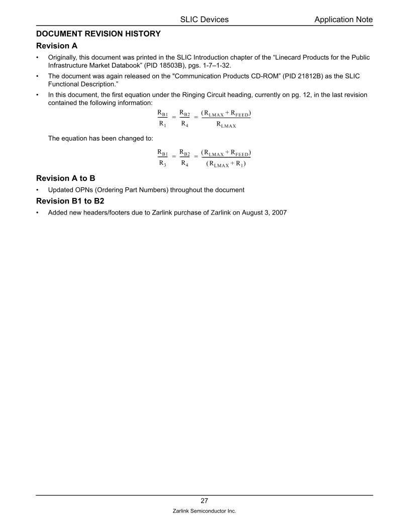
DOCUMENT REVISION HISTORYRevision A• Originally, this document was printed in the SLIC Introduction chapter of the “Linecard Products for the Public
Infrastructure Market Databook” (PID 18503B), pgs. 1-7–1-32.• The document was again released on the "Communication Products CD-ROM” (PID 21812B) as the SLIC
Functional Description.”• In this document, the first equation under the Ringing Circuit heading, currently on pg. 12, in the last revision
contained the following information:
The equation has been changed to:
Revision A to B• Updated OPNs (Ordering Part Numbers) throughout the document
Revision B1 to B2• Added new headers/footers due to Zarlink purchase of Zarlink on August 3, 2007
RB1R1---------
RB2R4--------- RLMAX RFEED+( )
RLMAX--------------------------------------------==
RB1R3---------
RB2R4--------- RLMAX RFEED+( )
RLMAX R1+( )--------------------------------------------==
27Zarlink Semiconductor Inc.

www.zarlink.com
Information relating to products and services furnished herein by Zarlink Semiconductor Inc. or its subsidiaries (collectively “Zarlink”) is believed to be reliable.However, Zarlink assumes no liability for errors that may appear in this publication, or for liability otherwise arising from the application or use of any suchinformation, product or service or for any infringement of patents or other intellectual property rights owned by third parties which may result from such application oruse. Neither the supply of such information or purchase of product or service conveys any license, either express or implied, under patents or other intellectualproperty rights owned by Zarlink or licensed from third parties by Zarlink, whatsoever. Purchasers of products are also hereby notified that the use of product incertain ways or in combination with Zarlink, or non-Zarlink furnished goods or services may infringe patents or other intellectual property rights owned by Zarlink.
This publication is issued to provide information only and (unless agreed by Zarlink in writing) may not be used, applied or reproduced for any purpose nor form partof any order or contract nor to be regarded as a representation relating to the products or services concerned. The products, their specifications, services and otherinformation appearing in this publication are subject to change by Zarlink without notice. No warranty or guarantee express or implied is made regarding thecapability, performance or suitability of any product or service. Information concerning possible methods of use is provided as a guide only and does not constituteany guarantee that such methods of use will be satisfactory in a specific piece of equipment. It is the user’s responsibility to fully determine the performance andsuitability of any equipment using such information and to ensure that any publication or data used is up to date and has not been superseded. Manufacturing doesnot necessarily include testing of all functions or parameters. These products are not suitable for use in any medical products whose failure to perform may result insignificant injury or death to the user. All products and materials are sold and services provided subject to Zarlink’s conditions of sale which are available on request.
Purchase of Zarlink’s I2C components conveys a license under the Philips I2C Patent rights to use these components in an I2C System, provided that the systemconforms to the I2C Standard Specification as defined by Philips.
Zarlink, ZL, the Zarlink Semiconductor logo and the Legerity logo and combinations thereof, VoiceEdge, VoicePort, SLAC, ISLIC, ISLAC and VoicePath aretrademarks of Zarlink Semiconductor Inc.
TECHNICAL DOCUMENTATION - NOT FOR RESALE
For more information about all Zarlink productsvisit our Web Site at